EP2341615A1 - OP-AMP sharing with input and output reset - Google Patents
OP-AMP sharing with input and output reset Download PDFInfo
- Publication number
- EP2341615A1 EP2341615A1 EP10196122A EP10196122A EP2341615A1 EP 2341615 A1 EP2341615 A1 EP 2341615A1 EP 10196122 A EP10196122 A EP 10196122A EP 10196122 A EP10196122 A EP 10196122A EP 2341615 A1 EP2341615 A1 EP 2341615A1
- Authority
- EP
- European Patent Office
- Prior art keywords
- differential
- pair
- input
- signal
- signals
- Prior art date
- Legal status (The legal status is an assumption and is not a legal conclusion. Google has not performed a legal analysis and makes no representation as to the accuracy of the status listed.)
- Granted
Links
Images


Classifications
-
- H—ELECTRICITY
- H03—ELECTRONIC CIRCUITRY
- H03F—AMPLIFIERS
- H03F3/00—Amplifiers with only discharge tubes or only semiconductor devices as amplifying elements
- H03F3/45—Differential amplifiers
-
- H—ELECTRICITY
- H03—ELECTRONIC CIRCUITRY
- H03F—AMPLIFIERS
- H03F3/00—Amplifiers with only discharge tubes or only semiconductor devices as amplifying elements
- H03F3/005—Amplifiers with only discharge tubes or only semiconductor devices as amplifying elements using switched capacitors, e.g. dynamic amplifiers; using switched capacitors as resistors in differential amplifiers
Definitions
- This disclosure relates generally to electronic circuits, and in particular, but not exclusively, is related to Switched Capacitor (SC) gain amplifiers and Pipelined Algorithmic Analog to Digital Converters (ADC).
- SC Switched Capacitor
- ADC Pipelined Algorithmic Analog to Digital Converters
- Pipelined Algorithmic Analog-to-Digital Converters are found in various applications, including image sensors, communication and television.
- a component found at each stage of a Pipelined Algorithmic ADC is an operational amplifier (OP-AMP).
- OP-AMP operational amplifier
- the majority of the power consumption of a pipeline ADC is in the OP-AMPs, so OP-AMP sharing is desirable to minimize the number of OP-AMPs used.
- amplification during a phase may be affected by a residue from a prior phase stored in capacitances of the OP-AMP input pair.
- the present application provides a amplifying apparatus comprising the features of claim 1, a method of amplifying a first differential pair of signals and a second differential pair of signals comprising the steps of claim 8.
- An operational amplifier with two pairs of differential inputs for use with an input switch capacitor network.
- the operational amplifier has reset devices for resetting the second pair of differential inputs while amplifying the first pair of differential inputs, and for resetting the first pair of differential inputs while amplifying the second pair of differential inputs for reducing memory effect in electronic circuits.
- Preferred embodiments are the subject of the dependent claims.
- the amplifier has an additional reset device for resetting the outputs during a prophase of amplifying the first pair of differential inputs and a prophase of amplifying the second pair of differential inputs.
- the operational amplifier has four inputs, a first and a second differential pairs, operational amplifier (OP-AMP) and outputs a single pair of differential output signals.
- Timing circuitry is provided for generating non-overlapping clocks.
- An input switched-capacitor (SC) network controlled by the non-overlapping clocks is configured such that the first pair of the differential input signals is amplified by the OP-AMP during a first phase, that the second pair of the differential input signals is amplified by the OP-AMP during a second phase.
- First input reset switch devices coupled between signals of the first pair of differential input signals and a reference signal, and second input reset switch devices coupled between signals of the second pair of differential input signals and the reference signal, are provided to reset the amplifier inputs.
- an additional reset device and signal is provided for resetting the amplifier output between amplification phases.
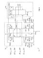
- FIG. 1 illustrates the SC gain amplifier with OP-AMP sharing with input and output reset according to an embodiment of the present invention.
- FIG. 2 illustrates the timing diagram of the SC gain amplifier and OP-AMP sharing with input and output reset according to an embodiment of the present invention.
- FIG. 3 illustrates the schematics of two-stage OP-AMP according to an embodiment of the present invention.
- the disclosed OP-AMP Rather than using OP-AMPs with one pair of differential inputs, the disclosed OP-AMP has two pairs of differential inputs, INPO-INNO and INP1-INN1, thereby allowing for input reset as well as output reset without having to insert a separate reset phase between clock cycles of the OP-AMP. If a reset phase is inserted between clock cycles of the OP-AMP, the operation of a functional block using said OP-AMP ⁇ such as a pipelined algorithmic ADC - may not be optimal because of the time required for a separate reset phase. Utilizing the disclosed OP-AMP in a pipelined algorithmic ADC may allow an increase in the operating clock speed of the pipeline ADC.
- the outputs of an SC network and differential inputs of the OP-AMP are reset using switches 113, 114, 113A, 114A, that selectively couple a pair of differential inputs together and to to a reference signal VREFC.
- the output of the OP-AMP is reset with an output reset switch 116 which selectively couples the signals VON, VOP of the differential output together.
- the SC network is coupled to the inputs of the OP-AMP, and has two capacitors 111, 112, 111A, 112A, 109, 110, 109A, and 110A coupled to each input of the SC network, and a pair of switches 101, 102, 103, 104, 105, 106, 107, 108, 101A, 102A, 103A, 104A, 105A, 106A, 107A, 108A coupled to each capacitor.
- Each pair of switches is controlled by one of two phase-clock signals, PH1 and PH2 as illustrated in FIG. 1 .
- the two phase-clock signals, PH1 and PH2 are non-overlapping as is illustrated in FIG. 2 .
- Phase-clock signals PH1 and PH2 alternately sample differential input signals VIN and VIP into capacitors of the SC network in a first phase (220), and cause the amplifier to amplify the difference between the sampled differential input signals with the OP-AMP in a second phase (210).
- input signals VIN and VIP are sampled again into capacitors of the SC network in the second phase (210), and the difference between the sampled differential input signals is amplified by the OP-AMP in the following first phase (220), the first and second phases alternating.
- gain is set by ratios of capacitances in the switched-capacitor network, such as ratios of capacitors 111 to 112, and 111A to 112A in the second phase, and similarly by ratios of capacitors 109 to 110 and 109A to 110A in the first phase.
- the INPO-INNO differential signal pair from the SC network are amplified through differential pair 311, 311A and selected by selectors 313, 313A during the first phase (220) when PH1B is high, and the INP1-INN1 differential signal pair are amplified by differential pair 314, 314A and enabled by selectors 316, 316A, during the second phase (210) when PH2B is high.
- first differential pair reset devices 312, 312A act to reset intermediate nodes between pair 311, 311A and selectors 313, 313A during the second phase when PH1 is high
- second differential pair reset devices 315, 315A act to reset intermediate nodes between pair 314, 314A and selectors 316, 316A during the first phase when PH2 is high
- Control signals PH1_0 and PH2_0 are also non-overlapping control signals, although PH1_0 overlaps PH1 and PH2_0 overlaps PH2.
- Non-overlapping control signals PH1_0 and PH2_0 reset a pair of differential inputs of the OP-AMP during a phase when the OP-AMP is not amplifying the sampled differential input signals.
- control signal PH1_0 is asserted when clock signal PH1 is asserted, and PH1_0 is de-asserted before the falling edge of clock signal PH1. Similar logic can be applied to control signal PH2_0 and clock signal PH2. In other embodiments control signal PH1_0 may be asserted before the rising edge of clock signal PH1, and/or may be de-asserted after the falling edge of clock signal PH2, as long as control signal PH1_0 does not overlap clock signal PH2.
- control signal PH2_0 which may be asserted before the rising edge of clock signal PH2, and/or may be de-asserted after the falling edge of clock signal PH2, as long as control signal PH2_0 is not asserted when clock PH1 is asserted.
- each pair of differential inputs of the OP-AMP is reset once, and the differential output of the OP-AMP is reset twice.
- An OP-AMP with two pairs of differential inputs allows for the frequent reset of its input and output without increasing the clock period of the OP-AMP.
- FIG. 1 illustrates a SC gain amplifier with OP-AMP sharing with input and output reset.
- OP-AMP 115 has two differential input pairs, INPO and INNO and INP and INN1. Note that since OP-AMP 115 is differential, only one side of the differential input pairs will be described.
- Each element in SC network coupled to a first differential input of OP-AMP 115 has a corresponding element coupled to a second differential input of OP-AMP 115.
- the first and second differential inputs make up one differential input pair.
- switch 101 couples differential output signal VON to differential input INPO of OP-AMP 115
- switch 101A couples differential output signal VOP to differential input INNO of OP-AMP 115. Similar logic can be applied to SC network elements 102A thru 114A.
- Inputs INPO and INP1 are connected to the SC subnetwork comprising switches 101-108 and capacitors 109-112. Two switches are connected to each capacitor, with switches 101 and 102 coupled to capacitor 109, switches 103 and 104 coupled to capacitor 110, switches 105 and 106 coupled to capacitor 111 and switches 107 and 108 coupled to capacitors 112, as shown in FIG. 1 .
- Switches 101 thru 108 are controlled by non-overlapping clocks PH1 and PH2.
- Switches 113 and 114 connect either INPO and INP1 respectively to reference signal VREFC to reset the signal.
- Switch 116 is coupled between the differential output, VON and VOP of OP-AMP 115.
- the disclosed switches are NMOS transistors, and it can be appreciated that clock signals PH1 and PH2 and control signals PH1_0 and PH2_0 are active-high signals.
- the disclosed switches which comprise the SC network may be PMOS transistors, in which case, clock signals PH1 and PH2, and control signals PH1_0 and PH2_0 are inverted to be active-low signals.
- the disclosed switches which comprise the SC network may be a combination of PMOS and NMOS transistors where clock signals which control the NMOS transistors are active-high and clock signals which control the PMOS transistors are active-low are used to obtain two non-overlapping phases for OP-AMP 115.
- a phase with clock signal PH1 asserted and clock signal PH2 deasserted is seen in time interval 210 in FIG. 2 .
- switches 102 and 104 are closed, and input signal VIN is sampled and stored in capacitors 109 and 110.
- control signal PH1_0 is asserted, and the OP-AMP input INPO is reset with reference signal VREFC.
- Switches 105 and 107 are also closed, and OP-AMP 115, output VON, is sampled at capacitor 111, while a reference signal, REF - OUTN1 is sampled at capacitor 112.
- input signal VIN is sampled at capacitors 109 and 110.
- control signal PH1_0 is de-asserted just before the falling edge of clock signal PH1.
- control signal PH1_0 may be asserted before the rising edge of clock signal PH1, and/or de-asserted after the falling edge of clock signal PH1, as long as control signal PH1_0 is not asserted when clock signal PH2 is asserted.
- control signal PH2_0 is de-asserted just before the falling edge of clock signal PH2. Similar logic can be applied to control signal PH2_0, which may be asserted before the rising edge of clock signal PH2, and/or may be de-asserted after the falling edge of clock signal PH2, as long as control signal PH2_0 is not asserted when clock PH1 is asserted.
- the differential output of OP-AMP 115 is selectively reset by switch 116 which is controlled by reset signal PH12_S.
- Reset signal PH12_S is pulsed at the rising edge of either clock signals PH1 or PH2.
- the reset of the differential output signal at every rising edge of clock signals PH1 and PH2 is provided to reduce the output memory effect.
- the rising edge of reset signal may occur before the rising edge of either clock signals PH1 or PH2.
- FIG. 2 illustrates an example of the timing of clock signals and control signals used in the SC network.
- the horizontal axis represents time and the vertical axis represents the amplitude of the signals.
- control signal PH1_0 is asserted and differential input pair INPO and INNO are reset with reference signal VREFC.
- Clock signal PH1 is asserted, and clock signal PH2 is de-asserted during this time interval, differential input pair INP1 and INN1 amplifies a signal sampled by capacitors 111 and 112.
- Input signal VIN is sampled at capacitors 109 and 110.
- control signal PH1_0 is deasserted.
- time interval 230 begins, and during this time interval clock signals PH1 and PH2, as well as control signals PH1_0 and PH2_0 are de-asserted, during this time, and none of the switches in the SC network are closed.
- control signal PH2_0 is asserted and differential input pair INP1 and INN1 are reset with reference signal VREFC differential.
- Clock signal PH2 is asserted, and clock signal PH1 is de-asserted during this time interval, differential input pair INPO and INNO amplifies the signal sampled by capacitors 109 and 110 at time interval 210.
- Input signal VIN is sampled at capacitors 111 and 112..
- control signal PH2_0 is deasserted.
- time interval 240 begins, and during the brief non-overlap interval clock signals PH1 and PH2, as well as control signals PH1_0 and PH2_0 are de-asserted, and none of the switches in the SC network are closed.
- control signal PH1_0 may be asserted before clock signal PH1 is asserted, in this case, time interval 240 may be shortened, or may not exist at all.
- Control signal PH1_0 also may be de-asserted after the falling edge of clock signal PH1; in this case, time interval 230 may be shortened, or may not exist at all, however some input offset error may be introduced by capacitive coupling associated with turning off these clocks if PH1_0 is not separate as illustrated. Similar logic may be applied to control signal PH2_0.
- FIG. 3 illustrates the OP-AMP, 115 as seen in FIG. 1 .
- OP-AMP 115 has two stages, telescopic OP-AMP stage 310 and common source OP-AMP stage 320.
- Signals CMFB1 and CMFB2 are common mode feedback signals for the first and second stage, 310 and 320 respectively and cascode compensation is used for stability.
- Differential output signals VON1 and VOP1 are the output of telescopic OP-AMP 310, and input of common source OP-AMP 320.
- Differential output signals VON and VOP are the output of the common source OP-AMP 320.
- Signals TCP, TCN, PB1, PB2, NB1 and PB1_OUT are bias voltage signals.
- Transistors 311 and 311A form one differential input pair, INPO and INN0, while transistors 314 and 314A form the second differential input pair, INP1 and INN1.
- transistors 311 and 311A are disconnected from the telescopic OP-AMP 310 and their drains are shorted via transistors 312 and 312A respectively.
- transistors 314 and 314A are connected through transistor 316 and 316A to CP and CN respectively.
- Transistors 312 and 312A in FIG. 3 ensure that the drains of 311 and 311A are reset to further reduce residual voltages from prior amplifer phases and cycles.
- the overlapping timing of complementary clock signals PH1B and PH2B ensure that at least one pair of differential input INP0 and INNO or INP1 and INN1 is coupled to the telescopic OP-AMP 310 at all times.
- transistors 314 and 314A are disconnected from the telescopic OP-AMP 310 and the drains of transistors 314 and 314A are shorted via transistors 315 and 315A respectively.
- transistors 311 and 311A are connected through transistors 313 and 313A to telescopic OP-AMP 310.
- Transistors 315 and 315A in FIG. 3 ensure that the drains of 314 and 314A are reset to further reduce residual voltages remaining in the amplifier from prior amplifier phases and cycles.
- the advantages of having two pairs of differential inputs include a reduction of power consumption. Most of the power consumed by a Pipeline ADC goes to the OP-AMP, and by time-sharing telescopic amplifier 310 and common source amplifier 320, the overall power consumption of each stage of the Pipeline ADC can decrease. Transistors 313, 313A, 316 and 316A ensure that at least one pair of differential inputs, INPO and INNO or INP1 and INN 1 is coupled to the telescopic OP-AMP 310 at all times. Another advantage of having two pairs of differential inputs is that a pair of differential inputs can be reset without inserting a full reset phase between clock cycles.
- the output of OP-AMP 115 is the differential pair VON, VOP, as previously mentioned in FIG. 1 .
- VON and VOP can be reset using switch 116 which is controlled by signal PH12_S.
- the signal PH12_S is pulsed at the rising edge of either PH1 or PH2, and the frequent reset of this output signal may reduce the occurrence of memory effect in image sensors.
- this disclosure can be applied to other SC circuits using different amplifiers, such as one-stage OP-AMP or OP-AMPs with PMOS input pairs instead of the NMOS pairs illustrated.
- the switches 101 - 108 and 113 and 114 in FIG. 1 which make up the SC network are shown as NMOS transistors.
- the switches which comprise the SC network could be PMOS transistors, or complimentary switches having a combination of NMOS and PMOS transistors.
- the illustrated OP-AMP has two pairs of differential inputs, it can be appreciated that the OP-AMP may have three, or four, or more pairs of differential inputs.
- One of the advantages of an OP-AMP with three or more pairs of differential inputs is that three or more stages of a Pipeline ADC may share a single OP-AMP, and therefore reduce the power consumption of the Pipeline ADC.
- the SC network will also need to be expanded to accommodate the additional pairs of inputs.
Landscapes
- Engineering & Computer Science (AREA)
- Power Engineering (AREA)
- Amplifiers (AREA)
Abstract
Description
- The present application claims priority to
U.S. Provisional Application Serial No. 61/289,956, filed December 23, 2009 - This disclosure relates generally to electronic circuits, and in particular, but not exclusively, is related to Switched Capacitor (SC) gain amplifiers and Pipelined Algorithmic Analog to Digital Converters (ADC).
- Due to their relatively simple implementation and low cost in the application of intermediate speed and resolution, Pipelined Algorithmic Analog-to-Digital Converters (ADC) are found in various applications, including image sensors, communication and television. A component found at each stage of a Pipelined Algorithmic ADC is an operational amplifier (OP-AMP). The majority of the power consumption of a pipeline ADC is in the OP-AMPs, so OP-AMP sharing is desirable to minimize the number of OP-AMPs used. However, without the use of a reset phase in an OP-AMP sharing structure to eliminate residual signals from prior phases, amplification during a phase may be affected by a residue from a prior phase stored in capacitances of the OP-AMP input pair. This problem becomes more pronounced when a large or full-swing input signal exists, for example, when an image sensor pixel is exposed to bright light, resulting in a white pixel, that may either be converted improperly or may affect conversion of a following pixel. This is an example of a phenomenon known as the memory effect.
- One method to reduce the occurrence of the memory effect in Pipeline ADCs is to insert a charge-reset phase between clock cycles. However, this has the effect of reducing the clock speed of the Pipeline ADC.
- The present application provides a amplifying apparatus comprising the features of claim 1, a method of amplifying a first differential pair of signals and a second differential pair of signals comprising the steps of claim 8. An operational amplifier with two pairs of differential inputs for use with an input switch capacitor network. The operational amplifier has reset devices for resetting the second pair of differential inputs while amplifying the first pair of differential inputs, and for resetting the first pair of differential inputs while amplifying the second pair of differential inputs for reducing memory effect in electronic circuits.
Preferred embodiments are the subject of the dependent claims.
In an embodiment, the amplifier has an additional reset device for resetting the outputs during a prophase of amplifying the first pair of differential inputs and a prophase of amplifying the second pair of differential inputs. - In an embodiment, the operational amplifier has four inputs, a first and a second differential pairs, operational amplifier (OP-AMP) and outputs a single pair of differential output signals. Timing circuitry is provided for generating non-overlapping clocks. An input switched-capacitor (SC) network controlled by the non-overlapping clocks is configured such that the first pair of the differential input signals is amplified by the OP-AMP during a first phase, that the second pair of the differential input signals is amplified by the OP-AMP during a second phase. First input reset switch devices, coupled between signals of the first pair of differential input signals and a reference signal, and second input reset switch devices coupled between signals of the second pair of differential input signals and the reference signal, are provided to reset the amplifier inputs. In an embodiment, an additional reset device and signal is provided for resetting the amplifier output between amplification phases.
- The embodiments are more fully appreciated in connection with the following detailed description taken in conjunction with the accompanying drawings, in which like reference characters refer to like parts throughout.
-
FIG. 1 illustrates the SC gain amplifier with OP-AMP sharing with input and output reset according to an embodiment of the present invention. -
FIG. 2 illustrates the timing diagram of the SC gain amplifier and OP-AMP sharing with input and output reset according to an embodiment of the present invention. -
FIG. 3 illustrates the schematics of two-stage OP-AMP according to an embodiment of the present invention. - An embodiment of the disclosed switched capacitor (SC) gain amplifier with OP-AMP sharing with input and output reset is described herein. In the following description numerous specific details are set forth to provide a thorough understanding of the embodiments. One skilled in the relevant art will recognize, however, that the techniques described herein can be practiced without one or more of the specific details, or with other methods, components, materials, etc.
- Rather than using OP-AMPs with one pair of differential inputs, the disclosed OP-AMP has two pairs of differential inputs, INPO-INNO and INP1-INN1, thereby allowing for input reset as well as output reset without having to insert a separate reset phase between clock cycles of the OP-AMP. If a reset phase is inserted between clock cycles of the OP-AMP, the operation of a functional block using said OP-AMP ― such as a pipelined algorithmic ADC - may not be optimal because of the time required for a separate reset phase. Utilizing the disclosed OP-AMP in a pipelined algorithmic ADC may allow an increase in the operating clock speed of the pipeline ADC.
- In the present amplifier, the outputs of an SC network and differential inputs of the OP-AMP are reset using
switches output reset switch 116 which selectively couples the signals VON, VOP of the differential output together. - The SC network is coupled to the inputs of the OP-AMP, and has two
capacitors switches FIG. 1 . The two phase-clock signals, PH1 and PH2, are non-overlapping as is illustrated inFIG. 2 . Phase-clock signals PH1 and PH2 alternately sample differential input signals VIN and VIP into capacitors of the SC network in a first phase (220), and cause the amplifier to amplify the difference between the sampled differential input signals with the OP-AMP in a second phase (210). Similarly input signals VIN and VIP are sampled again into capacitors of the SC network in the second phase (210), and the difference between the sampled differential input signals is amplified by the OP-AMP in the following first phase (220), the first and second phases alternating. In both phases, gain is set by ratios of capacitances in the switched-capacitor network, such as ratios ofcapacitors 111 to 112, and 111A to 112A in the second phase, and similarly by ratios ofcapacitors 109 to 110 and 109A to 110A in the first phase. - As can be seen in
FIG. 3 with reference toFIG. 2 , the INPO-INNO differential signal pair from the SC network are amplified throughdifferential pair selectors differential pair selectors 316, 316A, during the second phase (210) when PH2B is high. Similarly, first differentialpair reset devices pair selectors pair reset devices pair selectors 316, 316A during the first phase when PH2 is high - Control signals PH1_0 and PH2_0 are also non-overlapping control signals, although PH1_0 overlaps PH1 and PH2_0 overlaps PH2. Non-overlapping control signals PH1_0 and PH2_0 reset a pair of differential inputs of the OP-AMP during a phase when the OP-AMP is not amplifying the sampled differential input signals.
- In the present embodiment, as seen in
FIG. 2 , control signal PH1_0 is asserted when clock signal PH1 is asserted, and PH1_0 is de-asserted before the falling edge of clock signal PH1. Similar logic can be applied to control signal PH2_0 and clock signal PH2. In other embodiments control signal PH1_0 may be asserted before the rising edge of clock signal PH1, and/or may be de-asserted after the falling edge of clock signal PH2, as long as control signal PH1_0 does not overlap clock signal PH2. Again, similar logic can be applied to control signal PH2_0, which may be asserted before the rising edge of clock signal PH2, and/or may be de-asserted after the falling edge of clock signal PH2, as long as control signal PH2_0 is not asserted when clock PH1 is asserted. During each clock cycle, each pair of differential inputs of the OP-AMP is reset once, and the differential output of the OP-AMP is reset twice. An OP-AMP with two pairs of differential inputs allows for the frequent reset of its input and output without increasing the clock period of the OP-AMP. - In more detail,
FIG. 1 illustrates a SC gain amplifier with OP-AMP sharing with input and output reset. OP-AMP 115 has two differential input pairs, INPO and INNO and INP and INN1. Note that since OP-AMP 115 is differential, only one side of the differential input pairs will be described. Each element in SC network coupled to a first differential input of OP-AMP 115 has a corresponding element coupled to a second differential input of OP-AMP 115. The first and second differential inputs make up one differential input pair. For example, switch 101 couples differential output signal VON to differential input INPO of OP-AMP 115,switch 101A couples differential output signal VOP to differential input INNO of OP-AMP 115. Similar logic can be applied to SC network elements 102A thru 114A. - Inputs INPO and INP1 are connected to the SC subnetwork comprising switches 101-108 and capacitors 109-112. Two switches are connected to each capacitor, with
switches capacitor 109,switches 103 and 104 coupled tocapacitor 110,switches 105 and 106 coupled tocapacitor 111 andswitches 107 and 108 coupled to capacitors 112, as shown inFIG. 1 .Switches 101 thru 108 are controlled by non-overlapping clocks PH1 and PH2. Switches 113 and 114 connect either INPO and INP1 respectively to reference signal VREFC to reset the signal.Switch 116 is coupled between the differential output, VON and VOP of OP-AMP 115. - When a signal is asserted, a switch which is controlled by that signal is closed, when the signal is deasserted, the switch which is controlled by that signal is open. In the present embodiment, the disclosed switches are NMOS transistors, and it can be appreciated that clock signals PH1 and PH2 and control signals PH1_0 and PH2_0 are active-high signals. In other embodiments of the invention, the disclosed switches which comprise the SC network may be PMOS transistors, in which case, clock signals PH1 and PH2, and control signals PH1_0 and PH2_0 are inverted to be active-low signals. In yet other embodiments of the present invention, the disclosed switches which comprise the SC network may be a combination of PMOS and NMOS transistors where clock signals which control the NMOS transistors are active-high and clock signals which control the PMOS transistors are active-low are used to obtain two non-overlapping phases for OP-
AMP 115. - A phase with clock signal PH1 asserted and clock signal PH2 deasserted is seen in
time interval 210 inFIG. 2 . In this phase, switches 102 and 104 are closed, and input signal VIN is sampled and stored incapacitors Switches AMP 115, output VON, is sampled atcapacitor 111, while a reference signal, REF - OUTN1 is sampled at capacitor 112.Capacitors 111 and 112, along with OP-AMP 115, form an SC gain amplifier having gain determined by a ratio of capacitance between capacitor 112 tocapacitor 111. In the same phase, input signal VIN is sampled atcapacitors - An alternate phase with clock signal PH2 is asserted and clock signal PH1 is deasserted as seen in
time interval 220 inFIG. 2 , switches 106 and 108 are closed and input signal VIN is sampled and stored incapacitors 111 and 112. During this time, control signal PH2_0 is asserted, and the OP-AMP input INP1 is reset with reference signal VREFC.Switches 101 and 103 are also closed, signal VON is sampled atcapacitor 109 and reference signal, REF_OUTN0 is sampled atcapacitor 110.Capacitors AMP 115 form an SC gain amplifier. The differential input INP1 is reset with reference signal VREFC, while input signal VIN is sampled atcapacitors 111 and 112. In the present embodiment, control signal PH2_0 is de-asserted just before the falling edge of clock signal PH2. Similar logic can be applied to control signal PH2_0, which may be asserted before the rising edge of clock signal PH2, and/or may be de-asserted after the falling edge of clock signal PH2, as long as control signal PH2_0 is not asserted when clock PH1 is asserted. - Clock signals PH1 and PH2 as well as their complements PH1B and PH2B control OP-
AMP 115. A schematic showing representative circuitry of OP-AMP 115 can is illustrated inFIG. 3 . The differential output of OP-AMP 115 is selectively reset byswitch 116 which is controlled by reset signal PH12_S. Reset signal PH12_S is pulsed at the rising edge of either clock signals PH1 or PH2. The reset of the differential output signal at every rising edge of clock signals PH1 and PH2 is provided to reduce the output memory effect. The rising edge of reset signal may occur before the rising edge of either clock signals PH1 or PH2. -
FIG. 2 illustrates an example of the timing of clock signals and control signals used in the SC network. InFIG. 2 , the horizontal axis represents time and the vertical axis represents the amplitude of the signals. Duringtime interval 210, control signal PH1_0 is asserted and differential input pair INPO and INNO are reset with reference signal VREFC. Clock signal PH1 is asserted, and clock signal PH2 is de-asserted during this time interval, differential input pair INP1 and INN1 amplifies a signal sampled bycapacitors 111 and 112. Input signal VIN is sampled atcapacitors time interval 230 begins, and during this time interval clock signals PH1 and PH2, as well as control signals PH1_0 and PH2_0 are de-asserted, during this time, and none of the switches in the SC network are closed. - During
time interval 220, control signal PH2_0 is asserted and differential input pair INP1 and INN1 are reset with reference signal VREFC differential. Clock signal PH2 is asserted, and clock signal PH1 is de-asserted during this time interval, differential input pair INPO and INNO amplifies the signal sampled bycapacitors time interval 210. Input signal VIN is sampled atcapacitors 111 and 112.. Before the falling edge of clock signal PH2, control signal PH2_0 is deasserted. When clock signal PH2 is de-asserted,time interval 240 begins, and during the brief non-overlap interval clock signals PH1 and PH2, as well as control signals PH1_0 and PH2_0 are de-asserted, and none of the switches in the SC network are closed. - As previously mentioned, control signal PH1_0 may be asserted before clock signal PH1 is asserted, in this case,
time interval 240 may be shortened, or may not exist at all. Control signal PH1_0 also may be de-asserted after the falling edge of clock signal PH1; in this case,time interval 230 may be shortened, or may not exist at all, however some input offset error may be introduced by capacitive coupling associated with turning off these clocks if PH1_0 is not separate as illustrated. Similar logic may be applied to control signal PH2_0. -
FIG. 3 illustrates the OP-AMP, 115 as seen inFIG. 1 . OP-AMP 115 has two stages, telescopic OP-AMP stage 310 and common source OP-AMP stage 320. Signals CMFB1 and CMFB2 are common mode feedback signals for the first and second stage, 310 and 320 respectively and cascode compensation is used for stability. Differential output signals VON1 and VOP1 are the output of telescopic OP-AMP 310, and input of common source OP-AMP 320. Differential output signals VON and VOP are the output of the common source OP-AMP 320. Signals TCP, TCN, PB1, PB2, NB1 and PB1_OUT are bias voltage signals. -
Transistors transistors transistors AMP 310 and their drains are shorted viatransistors transistors transistor 316 and 316A to CP and CN respectively. - Recall in the previous discussion of
FIG. 1 , when PH1 is asserted, and PH2 is deasserted, the differential input pair INPO and INNO are reset with reference signal VREFC.Transistors FIG. 3 ensure that the drains of 311 and 311A are reset to further reduce residual voltages from prior amplifer phases and cycles. The overlapping timing of complementary clock signals PH1B and PH2B ensure that at least one pair of differential input INP0 and INNO or INP1 and INN1 is coupled to the telescopic OP-AMP 310 at all times. - When PH2 is asserted and PH1 is deasserted,
transistors AMP 310 and the drains oftransistors transistors transistors transistors AMP 310. - Recall in the previous discussion of
FIG. 1 , when PH2 is asserted, and PH1 is deasserted, the differential input pair INP1 and INN1 are reset with reference signal VREFC.Transistors FIG. 3 ensure that the drains of 314 and 314A are reset to further reduce residual voltages remaining in the amplifier from prior amplifier phases and cycles. - The advantages of having two pairs of differential inputs include a reduction of power consumption. Most of the power consumed by a Pipeline ADC goes to the OP-AMP, and by time-sharing
telescopic amplifier 310 andcommon source amplifier 320, the overall power consumption of each stage of the Pipeline ADC can decrease.Transistors AMP 310 at all times. Another advantage of having two pairs of differential inputs is that a pair of differential inputs can be reset without inserting a full reset phase between clock cycles. - The output of OP-
AMP 115 is the differential pair VON, VOP, as previously mentioned inFIG. 1 . VON and VOP can be reset usingswitch 116 which is controlled by signal PH12_S. The signal PH12_S is pulsed at the rising edge of either PH1 or PH2, and the frequent reset of this output signal may reduce the occurrence of memory effect in image sensors. - It can be appreciated that this disclosure can be applied to other SC circuits using different amplifiers, such as one-stage OP-AMP or OP-AMPs with PMOS input pairs instead of the NMOS pairs illustrated. In the present embodiment, the switches 101 - 108 and 113 and 114 in
FIG. 1 which make up the SC network are shown as NMOS transistors. The switches which comprise the SC network could be PMOS transistors, or complimentary switches having a combination of NMOS and PMOS transistors. - While the illustrated OP-AMP has two pairs of differential inputs, it can be appreciated that the OP-AMP may have three, or four, or more pairs of differential inputs. One of the advantages of an OP-AMP with three or more pairs of differential inputs is that three or more stages of a Pipeline ADC may share a single OP-AMP, and therefore reduce the power consumption of the Pipeline ADC. In the case of an OP-AMP with three or more pairs of differential inputs, the SC network will also need to be expanded to accommodate the additional pairs of inputs.
The foregoing description, for purposes of explanation, used specific nomenclature to provide a thorough understanding of the various embodiments. However, it will be apparent to one skilled in the art that specific details are not required in order to practice the embodiments as described. Thus, the foregoing descriptions of specific embodiments are presented for purposes of illustration and description. They are not intended to be exhaustive or to limit the embodiments to the precise forms disclosed; obviously, many modifications and variations are possible in view of the above teachings.
Claims (9)
- An amplifying apparatus comprising:a four-input operational amplifier (OP-AMP); whereinsaid four-input OP-AMP receives a first and a second pair of differential input signals and outputs a pair of differential output signals; whereineach of the first and second pair of differential input signals comprises a first and a second signal;timing circuitry for generating a first and a second non-overlapping clock;an input switched-capacitor (SC) network controlled by the first and second non-overlapping clocks and configured such that the first pair of the differential input signals is amplified by the OP-AMP during a first phase, that the second pair of the differential input signals is amplified by the OP-AMP during the second phase, the first phase non-overlapping and alternating with the second phase;first input reset switch devices coupled between the first signal and the second signal of the first pair of differential input signals and a reference signal, and second input reset switch devices coupled between the first signal and the second signal of the second pair of differential input signals and the reference signal; whereineach of said input reset switches is controlled by a signal selected from the group consisting of a first and a second control signals;and said first and second control signals are non-overlapping.
- The apparatus of claim 1 further comprising an output reset switch device controlled by a third clock, the output reset switch device coupled between said pair of differential output signals to selectively couple said pair of differential output signals; and wherein the timing circuitry generates the third clock to enable the reset switch during a prophase of both the first phase and the second phase.
- The apparatus of claim 1 or claim 2 wherein the timing circuitry further generates the first and second control signals, wherein the first control signal is active during at least a portion of the second phase, and the second control signal is active during at least a portion of the first phase.
- The apparatus of claim 1, 2, or claim 3, wherein:said four-input OP-AMP comprises:a first transistor having a gate for coupling to a first differential input signal of the first pair of differential input signals;a second transistor having a gate for coupling to a second differential input signal of the first pair of differential input signals;a third transistor having a gate for coupling to a first differential input signal of the second pair of differential input signals; anda fourth transistor having a gate for coupling to a second differential input signal of the second pair of differential input signals;said OP-AMP is configured and arranged such that a drain of each transistor is reset when a reference signal is applied to the gate of the transistor.
- The apparatus of claim 4 wherein a source of the first, second, third and fourth transistor are coupled together to a current source.
- The apparatus of claim 4 or 5 wherein:the drain of the first transistor is coupled to a source of a first switching transistor, the drain of the second transistor is coupled to a source of a second switching transistor, the drain of the third transistor is coupled to a source of a third switching transistor, the drain of the fourth transistor is coupled to a source of a fourth switching transistor; andwherein a gate of the second switching transistor is coupled to a gate of the first switching transistor and to a clock active during the first phase, and wherein a gate of the third switching transistor is coupled to a gate of the fourth switching transistor and to a clock active during the second phase.
- The apparatus of any one of the preceding claims, wherein:said four-input OP-AMP comprises:a telescopic OP-AMP stage,a first differential input pair for coupling said first pair of differential input signals to an input pair of said telescopic OP-AMP stage, and
a second differential input pair for coupling said second pair of differential input signals to said input pair of said telescopic OP-AMP stage;said four-input OP-AMP is configured and arranged such that at least one of said first and second differential input pairs is connected to said input pair of said telescopic OP-AMP at all times during operation of the apparatus. - A method of amplifying a first differential pair of signals and a second differential pair of signals comprising:applying the first differential signal to a first differential pair, and selecting the first differential pair as an active input pair of a differential amplifier;amplifying the first differential signal to provide a first amplified output on differential output signals;applying the second differential signal to a second differential pair, and selecting the second differential pair as the active input pair of the differential amplifier; resetting the output signals to eliminate residual effects of the first amplified output; resetting the first differential pair;amplifying the second differential signal to provide a second amplified output on the differential output signals;resetting the second differential pair; andresetting the output signals to eliminate residual effects of the second amplified output.
- The method of claim 8 further comprising using feedback from the differential output signals to a switched capacitor network having gain capacitors to determine a gain of the step of amplifying the first differential signal; and using feedback from the differential output signals to the switched capacitor network to determine a gain of the step of amplifying the second differential signal.
Applications Claiming Priority (1)
| Application Number | Priority Date | Filing Date | Title |
|---|---|---|---|
| US28995609P | 2009-12-23 | 2009-12-23 |
Publications (2)
| Publication Number | Publication Date |
|---|---|
| EP2341615A1 true EP2341615A1 (en) | 2011-07-06 |
| EP2341615B1 EP2341615B1 (en) | 2013-03-13 |
Family
ID=43857874
Family Applications (1)
| Application Number | Title | Priority Date | Filing Date |
|---|---|---|---|
| EP10196122A Active EP2341615B1 (en) | 2009-12-23 | 2010-12-21 | OP-AMP sharing with input and output reset |
Country Status (4)
| Country | Link |
|---|---|
| US (1) | US8120423B2 (en) |
| EP (1) | EP2341615B1 (en) |
| CN (1) | CN102111115B (en) |
| TW (1) | TWI427921B (en) |
Families Citing this family (10)
| Publication number | Priority date | Publication date | Assignee | Title |
|---|---|---|---|---|
| US8680915B1 (en) | 2011-11-29 | 2014-03-25 | Agilent Technologies, Inc. | Techniques to reduce memory effect or inter-symbol interference (ISI) in circuits using op-amp sharing |
| US8643432B1 (en) | 2012-07-27 | 2014-02-04 | Hong Kong Applied Science & Technology Research Institute Company Ltd. | Op-Amp sharing by swapping trans-conductance cells |
| JP6291316B2 (en) * | 2014-03-31 | 2018-03-14 | 株式会社メガチップス | Semiconductor circuit and amplifier circuit |
| CN106160745B (en) * | 2015-03-31 | 2019-05-24 | 智原微电子(苏州)有限公司 | Analog-digital commutator and its initial method |
| KR102509819B1 (en) * | 2015-11-04 | 2023-03-14 | 삼성전자주식회사 | Signal processing apparatus and signal processing method |
| CN116419085A (en) * | 2017-11-30 | 2023-07-11 | 索尼半导体解决方案公司 | Light detection device |
| FR3087062B1 (en) | 2018-10-09 | 2021-05-07 | St Microelectronics Rousset | POWER STAGE CONTROL OF A SWITCHING POWER SUPPLY |
| FR3087063B1 (en) * | 2018-10-09 | 2021-05-28 | St Microelectronics Rousset | NON-OVERLAPPING SIGNAL GENERATION CIRCUIT |
| JP7374586B2 (en) * | 2019-01-17 | 2023-11-07 | ブリルニクス シンガポール プライベート リミテッド | Solid-state imaging device, driving method for solid-state imaging device, and electronic equipment |
| US11424726B2 (en) * | 2020-04-01 | 2022-08-23 | Taiwan Semiconductor Manufacturing Company, Ltd. | Differential amplifier |
Citations (3)
| Publication number | Priority date | Publication date | Assignee | Title |
|---|---|---|---|---|
| EP0829955A1 (en) * | 1996-09-13 | 1998-03-18 | ALCATEL BELL Naamloze Vennootschap | Low noise amplifier structure |
| US7250813B1 (en) * | 2005-10-21 | 2007-07-31 | National Semiconductor Corporation | Split amplifier architecture for cross talk cancellation |
| US7345530B1 (en) * | 2006-06-01 | 2008-03-18 | National Semiconductor Corporation | Regulated switch driving scheme in switched-capacitor amplifiers with opamp-sharing |
Family Cites Families (12)
| Publication number | Priority date | Publication date | Assignee | Title |
|---|---|---|---|---|
| US5990707A (en) * | 1997-09-05 | 1999-11-23 | Cirrus Logic, Inc. | Method and system for sliced integration of flash analog to digital converters in read channel circuits |
| GB2358097A (en) * | 1999-12-22 | 2001-07-11 | Ericsson Telefon Ab L M | A low voltage switched capacitor differential amplifier with improved dynamic range |
| JP4524061B2 (en) * | 2002-03-26 | 2010-08-11 | パナソニック株式会社 | Reference voltage generator and voltage amplifier using the same |
| US6791378B2 (en) * | 2002-08-19 | 2004-09-14 | Micron Technology, Inc. | Charge recycling amplifier for a high dynamic range CMOS imager |
| US6956519B1 (en) * | 2004-10-11 | 2005-10-18 | Faraday Technology Corp. | Switched capacitor circuit of a pipeline analog to digital converter and a method for operating the switched capacitor circuit |
| US7609303B1 (en) * | 2004-10-12 | 2009-10-27 | Melexis Tessenderlo Nv | Low noise active pixel image sensor using a modified reset value |
| US7733168B2 (en) * | 2005-11-21 | 2010-06-08 | Panasonic Corporation | Fully differential comparator and fully differential amplifier |
| EP2005582B1 (en) * | 2006-03-23 | 2011-09-14 | Nxp B.V. | Converter with parallel coupled differential input pairs |
| CN100428631C (en) * | 2006-06-23 | 2008-10-22 | 清华大学 | A Method of Reducing Capacitance Mismatch Error of Analog-to-Digital Converter Based on Capacitor Pairing |
| US7633423B2 (en) * | 2007-11-02 | 2009-12-15 | Micron Technology, Inc. | Method of and apparatus for reducing settling time of a switched capacitor amplifier |
| US7639073B2 (en) * | 2007-11-16 | 2009-12-29 | Omnivision Technologies, Inc. | Switched-capacitor amplifier with improved reset phase |
| JP2011015248A (en) * | 2009-07-03 | 2011-01-20 | Renesas Electronics Corp | Differential chopper comparator and a/d converter circuit including the same |
-
2010
- 2010-12-06 US US12/960,858 patent/US8120423B2/en active Active
- 2010-12-07 TW TW099142616A patent/TWI427921B/en active
- 2010-12-21 EP EP10196122A patent/EP2341615B1/en active Active
- 2010-12-22 CN CN201010600175.8A patent/CN102111115B/en active Active
Patent Citations (3)
| Publication number | Priority date | Publication date | Assignee | Title |
|---|---|---|---|---|
| EP0829955A1 (en) * | 1996-09-13 | 1998-03-18 | ALCATEL BELL Naamloze Vennootschap | Low noise amplifier structure |
| US7250813B1 (en) * | 2005-10-21 | 2007-07-31 | National Semiconductor Corporation | Split amplifier architecture for cross talk cancellation |
| US7345530B1 (en) * | 2006-06-01 | 2008-03-18 | National Semiconductor Corporation | Regulated switch driving scheme in switched-capacitor amplifiers with opamp-sharing |
Non-Patent Citations (3)
| Title |
|---|
| CENTURELLI F ET AL: "Switched Capacitor Sample-and-Hold Circuit with Input Signal Range beyond Supply Voltage", NORCHIP, 2008, IEEE, PISCATAWAY, NJ, USA, 16 November 2008 (2008-11-16), pages 75 - 78, XP031401111, ISBN: 978-1-4244-2492-4 * |
| KAMARAINEN M ET AL: "A Micropower Front End for Three-Axis Capacitive Microaccelerometers", IEEE TRANSACTIONS ON INSTRUMENTATION AND MEASUREMENT, IEEE SERVICE CENTER, PISCATAWAY, NJ, US, vol. 58, no. 10, 1 October 2009 (2009-10-01), pages 3642 - 3652, XP011269690, ISSN: 0018-9456, DOI: 10.1109/TIM.2009.2018700 * |
| U-FAT CHIO ET AL: "Comparator-based successive folding ADC", MICROELECTRONICS&ELECTRONICS, 2009. PRIMEASIA 2009. ASIA PACIFIC CONFERENCE ON POSTGRADUATE RESEARCH IN, IEEE, PISCATAWAY, NJ, USA, 19 January 2009 (2009-01-19), pages 117 - 120, XP031617961, ISBN: 978-1-4244-4668-1 * |
Also Published As
| Publication number | Publication date |
|---|---|
| TW201136143A (en) | 2011-10-16 |
| TWI427921B (en) | 2014-02-21 |
| US20110148523A1 (en) | 2011-06-23 |
| US8120423B2 (en) | 2012-02-21 |
| CN102111115B (en) | 2014-11-05 |
| CN102111115A (en) | 2011-06-29 |
| EP2341615B1 (en) | 2013-03-13 |
Similar Documents
| Publication | Publication Date | Title |
|---|---|---|
| EP2341615B1 (en) | OP-AMP sharing with input and output reset | |
| US7154294B2 (en) | Comparators capable of output offset calibration | |
| US5963156A (en) | Sample and hold circuit and method with common mode differential signal feedback for converting single-ended signals to differential signals | |
| US7733169B2 (en) | Slew rate and settling time improvement circuitry and method for 3-stage amplifier | |
| US7633423B2 (en) | Method of and apparatus for reducing settling time of a switched capacitor amplifier | |
| US9973179B2 (en) | Sense amplifier latch with offset correction | |
| CN106712730B (en) | An adjustable signal and programmable gain amplifier | |
| US7868810B2 (en) | Amplifier circuit and A/D converter | |
| US9548948B2 (en) | Input current cancellation scheme for fast channel switching systems | |
| US7746260B1 (en) | Multiplying digital-to-analog converter for high speed and low supply voltage | |
| EP2220764B1 (en) | Switched-capacitor amplifier with improved reset phase | |
| JP5136587B2 (en) | Amplifier circuit, signal processing circuit, and semiconductor integrated circuit device | |
| US20070194850A1 (en) | Dynamically compensated operational amplifier | |
| WO2016203525A1 (en) | Semiconductor device | |
| US7167029B2 (en) | Sampling and level shifting circuit | |
| US7279940B1 (en) | Switched-capacitor circuit with time-shifted switching scheme | |
| US7920022B2 (en) | Switched capacitor system with and method for output glitch reduction | |
| EP2293434B1 (en) | Switched amplifier circuit arrangement and method for switched amplification | |
| US7449950B2 (en) | Analog signal processing circuit | |
| US7459943B2 (en) | High accuracy sample and hold circuit having a common negative input terminal | |
| KR102839770B1 (en) | An amplifier circuit and method for controlling a gain-bandwidth of an operational amplifier | |
| JP6155918B2 (en) | Sample and hold circuit, analog-digital conversion circuit, and digital control circuit | |
| US10715758B2 (en) | Amplification circuit performing primary and secondary amplifications | |
| JP2013207697A (en) | Sample hold circuit | |
| CN115765741B (en) | ADC driving interface circuit |
Legal Events
| Date | Code | Title | Description |
|---|---|---|---|
| PUAI | Public reference made under article 153(3) epc to a published international application that has entered the european phase |
Free format text: ORIGINAL CODE: 0009012 |
|
| AK | Designated contracting states |
Kind code of ref document: A1 Designated state(s): AL AT BE BG CH CY CZ DE DK EE ES FI FR GB GR HR HU IE IS IT LI LT LU LV MC MK MT NL NO PL PT RO RS SE SI SK SM TR |
|
| AX | Request for extension of the european patent |
Extension state: BA ME |
|
| 17P | Request for examination filed |
Effective date: 20120105 |
|
| GRAP | Despatch of communication of intention to grant a patent |
Free format text: ORIGINAL CODE: EPIDOSNIGR1 |
|
| GRAS | Grant fee paid |
Free format text: ORIGINAL CODE: EPIDOSNIGR3 |
|
| GRAA | (expected) grant |
Free format text: ORIGINAL CODE: 0009210 |
|
| AK | Designated contracting states |
Kind code of ref document: B1 Designated state(s): AL AT BE BG CH CY CZ DE DK EE ES FI FR GB GR HR HU IE IS IT LI LT LU LV MC MK MT NL NO PL PT RO RS SE SI SK SM TR |
|
| REG | Reference to a national code |
Ref country code: GB Ref legal event code: FG4D |
|
| REG | Reference to a national code |
Ref country code: AT Ref legal event code: REF Ref document number: 601305 Country of ref document: AT Kind code of ref document: T Effective date: 20130315 Ref country code: CH Ref legal event code: EP |
|
| REG | Reference to a national code |
Ref country code: IE Ref legal event code: FG4D |
|
| REG | Reference to a national code |
Ref country code: CH Ref legal event code: NV Representative=s name: BOHEST AG, CH |
|
| REG | Reference to a national code |
Ref country code: DE Ref legal event code: R096 Ref document number: 602010005427 Country of ref document: DE Effective date: 20130508 |
|
| PG25 | Lapsed in a contracting state [announced via postgrant information from national office to epo] |
Ref country code: LT Free format text: LAPSE BECAUSE OF FAILURE TO SUBMIT A TRANSLATION OF THE DESCRIPTION OR TO PAY THE FEE WITHIN THE PRESCRIBED TIME-LIMIT Effective date: 20130313 Ref country code: SE Free format text: LAPSE BECAUSE OF FAILURE TO SUBMIT A TRANSLATION OF THE DESCRIPTION OR TO PAY THE FEE WITHIN THE PRESCRIBED TIME-LIMIT Effective date: 20130313 Ref country code: BG Free format text: LAPSE BECAUSE OF FAILURE TO SUBMIT A TRANSLATION OF THE DESCRIPTION OR TO PAY THE FEE WITHIN THE PRESCRIBED TIME-LIMIT Effective date: 20130613 Ref country code: NO Free format text: LAPSE BECAUSE OF FAILURE TO SUBMIT A TRANSLATION OF THE DESCRIPTION OR TO PAY THE FEE WITHIN THE PRESCRIBED TIME-LIMIT Effective date: 20130613 Ref country code: ES Free format text: LAPSE BECAUSE OF FAILURE TO SUBMIT A TRANSLATION OF THE DESCRIPTION OR TO PAY THE FEE WITHIN THE PRESCRIBED TIME-LIMIT Effective date: 20130624 |
|
| REG | Reference to a national code |
Ref country code: AT Ref legal event code: MK05 Ref document number: 601305 Country of ref document: AT Kind code of ref document: T Effective date: 20130313 |
|
| REG | Reference to a national code |
Ref country code: NL Ref legal event code: VDEP Effective date: 20130313 |
|
| REG | Reference to a national code |
Ref country code: LT Ref legal event code: MG4D |
|
| PG25 | Lapsed in a contracting state [announced via postgrant information from national office to epo] |
Ref country code: FI Free format text: LAPSE BECAUSE OF FAILURE TO SUBMIT A TRANSLATION OF THE DESCRIPTION OR TO PAY THE FEE WITHIN THE PRESCRIBED TIME-LIMIT Effective date: 20130313 Ref country code: SI Free format text: LAPSE BECAUSE OF FAILURE TO SUBMIT A TRANSLATION OF THE DESCRIPTION OR TO PAY THE FEE WITHIN THE PRESCRIBED TIME-LIMIT Effective date: 20130313 Ref country code: GR Free format text: LAPSE BECAUSE OF FAILURE TO SUBMIT A TRANSLATION OF THE DESCRIPTION OR TO PAY THE FEE WITHIN THE PRESCRIBED TIME-LIMIT Effective date: 20130614 Ref country code: LV Free format text: LAPSE BECAUSE OF FAILURE TO SUBMIT A TRANSLATION OF THE DESCRIPTION OR TO PAY THE FEE WITHIN THE PRESCRIBED TIME-LIMIT Effective date: 20130313 |
|
| PG25 | Lapsed in a contracting state [announced via postgrant information from national office to epo] |
Ref country code: RS Free format text: LAPSE BECAUSE OF FAILURE TO SUBMIT A TRANSLATION OF THE DESCRIPTION OR TO PAY THE FEE WITHIN THE PRESCRIBED TIME-LIMIT Effective date: 20130313 Ref country code: BE Free format text: LAPSE BECAUSE OF FAILURE TO SUBMIT A TRANSLATION OF THE DESCRIPTION OR TO PAY THE FEE WITHIN THE PRESCRIBED TIME-LIMIT Effective date: 20130313 Ref country code: HR Free format text: LAPSE BECAUSE OF FAILURE TO SUBMIT A TRANSLATION OF THE DESCRIPTION OR TO PAY THE FEE WITHIN THE PRESCRIBED TIME-LIMIT Effective date: 20130313 |
|
| PG25 | Lapsed in a contracting state [announced via postgrant information from national office to epo] |
Ref country code: EE Free format text: LAPSE BECAUSE OF FAILURE TO SUBMIT A TRANSLATION OF THE DESCRIPTION OR TO PAY THE FEE WITHIN THE PRESCRIBED TIME-LIMIT Effective date: 20130313 Ref country code: SK Free format text: LAPSE BECAUSE OF FAILURE TO SUBMIT A TRANSLATION OF THE DESCRIPTION OR TO PAY THE FEE WITHIN THE PRESCRIBED TIME-LIMIT Effective date: 20130313 Ref country code: RO Free format text: LAPSE BECAUSE OF FAILURE TO SUBMIT A TRANSLATION OF THE DESCRIPTION OR TO PAY THE FEE WITHIN THE PRESCRIBED TIME-LIMIT Effective date: 20130313 Ref country code: PT Free format text: LAPSE BECAUSE OF FAILURE TO SUBMIT A TRANSLATION OF THE DESCRIPTION OR TO PAY THE FEE WITHIN THE PRESCRIBED TIME-LIMIT Effective date: 20130715 Ref country code: NL Free format text: LAPSE BECAUSE OF FAILURE TO SUBMIT A TRANSLATION OF THE DESCRIPTION OR TO PAY THE FEE WITHIN THE PRESCRIBED TIME-LIMIT Effective date: 20130313 Ref country code: AT Free format text: LAPSE BECAUSE OF FAILURE TO SUBMIT A TRANSLATION OF THE DESCRIPTION OR TO PAY THE FEE WITHIN THE PRESCRIBED TIME-LIMIT Effective date: 20130313 Ref country code: CZ Free format text: LAPSE BECAUSE OF FAILURE TO SUBMIT A TRANSLATION OF THE DESCRIPTION OR TO PAY THE FEE WITHIN THE PRESCRIBED TIME-LIMIT Effective date: 20130313 Ref country code: IS Free format text: LAPSE BECAUSE OF FAILURE TO SUBMIT A TRANSLATION OF THE DESCRIPTION OR TO PAY THE FEE WITHIN THE PRESCRIBED TIME-LIMIT Effective date: 20130713 |
|
| PG25 | Lapsed in a contracting state [announced via postgrant information from national office to epo] |
Ref country code: PL Free format text: LAPSE BECAUSE OF FAILURE TO SUBMIT A TRANSLATION OF THE DESCRIPTION OR TO PAY THE FEE WITHIN THE PRESCRIBED TIME-LIMIT Effective date: 20130313 |
|
| PLBE | No opposition filed within time limit |
Free format text: ORIGINAL CODE: 0009261 |
|
| STAA | Information on the status of an ep patent application or granted ep patent |
Free format text: STATUS: NO OPPOSITION FILED WITHIN TIME LIMIT |
|
| PG25 | Lapsed in a contracting state [announced via postgrant information from national office to epo] |
Ref country code: DK Free format text: LAPSE BECAUSE OF FAILURE TO SUBMIT A TRANSLATION OF THE DESCRIPTION OR TO PAY THE FEE WITHIN THE PRESCRIBED TIME-LIMIT Effective date: 20130313 |
|
| 26N | No opposition filed |
Effective date: 20131216 |
|
| PG25 | Lapsed in a contracting state [announced via postgrant information from national office to epo] |
Ref country code: IT Free format text: LAPSE BECAUSE OF FAILURE TO SUBMIT A TRANSLATION OF THE DESCRIPTION OR TO PAY THE FEE WITHIN THE PRESCRIBED TIME-LIMIT Effective date: 20130313 |
|
| REG | Reference to a national code |
Ref country code: DE Ref legal event code: R097 Ref document number: 602010005427 Country of ref document: DE Effective date: 20131216 |
|
| REG | Reference to a national code |
Ref country code: CH Ref legal event code: PCAR Free format text: NEW ADDRESS: HOLBEINSTRASSE 36-38, 4051 BASEL (CH) |
|
| PG25 | Lapsed in a contracting state [announced via postgrant information from national office to epo] |
Ref country code: LU Free format text: LAPSE BECAUSE OF FAILURE TO SUBMIT A TRANSLATION OF THE DESCRIPTION OR TO PAY THE FEE WITHIN THE PRESCRIBED TIME-LIMIT Effective date: 20131221 Ref country code: MC Free format text: LAPSE BECAUSE OF FAILURE TO SUBMIT A TRANSLATION OF THE DESCRIPTION OR TO PAY THE FEE WITHIN THE PRESCRIBED TIME-LIMIT Effective date: 20130313 |
|
| REG | Reference to a national code |
Ref country code: IE Ref legal event code: MM4A |
|
| PG25 | Lapsed in a contracting state [announced via postgrant information from national office to epo] |
Ref country code: IE Free format text: LAPSE BECAUSE OF NON-PAYMENT OF DUE FEES Effective date: 20131221 |
|
| PG25 | Lapsed in a contracting state [announced via postgrant information from national office to epo] |
Ref country code: SM Free format text: LAPSE BECAUSE OF FAILURE TO SUBMIT A TRANSLATION OF THE DESCRIPTION OR TO PAY THE FEE WITHIN THE PRESCRIBED TIME-LIMIT Effective date: 20130313 |
|
| PG25 | Lapsed in a contracting state [announced via postgrant information from national office to epo] |
Ref country code: TR Free format text: LAPSE BECAUSE OF FAILURE TO SUBMIT A TRANSLATION OF THE DESCRIPTION OR TO PAY THE FEE WITHIN THE PRESCRIBED TIME-LIMIT Effective date: 20130313 Ref country code: CY Free format text: LAPSE BECAUSE OF FAILURE TO SUBMIT A TRANSLATION OF THE DESCRIPTION OR TO PAY THE FEE WITHIN THE PRESCRIBED TIME-LIMIT Effective date: 20130313 |
|
| PG25 | Lapsed in a contracting state [announced via postgrant information from national office to epo] |
Ref country code: MK Free format text: LAPSE BECAUSE OF FAILURE TO SUBMIT A TRANSLATION OF THE DESCRIPTION OR TO PAY THE FEE WITHIN THE PRESCRIBED TIME-LIMIT Effective date: 20130313 Ref country code: HU Free format text: LAPSE BECAUSE OF FAILURE TO SUBMIT A TRANSLATION OF THE DESCRIPTION OR TO PAY THE FEE WITHIN THE PRESCRIBED TIME-LIMIT; INVALID AB INITIO Effective date: 20101221 |
|
| PG25 | Lapsed in a contracting state [announced via postgrant information from national office to epo] |
Ref country code: MT Free format text: LAPSE BECAUSE OF FAILURE TO SUBMIT A TRANSLATION OF THE DESCRIPTION OR TO PAY THE FEE WITHIN THE PRESCRIBED TIME-LIMIT Effective date: 20130313 |
|
| REG | Reference to a national code |
Ref country code: FR Ref legal event code: PLFP Year of fee payment: 6 |
|
| REG | Reference to a national code |
Ref country code: FR Ref legal event code: PLFP Year of fee payment: 7 |
|
| REG | Reference to a national code |
Ref country code: FR Ref legal event code: PLFP Year of fee payment: 8 |
|
| PG25 | Lapsed in a contracting state [announced via postgrant information from national office to epo] |
Ref country code: AL Free format text: LAPSE BECAUSE OF FAILURE TO SUBMIT A TRANSLATION OF THE DESCRIPTION OR TO PAY THE FEE WITHIN THE PRESCRIBED TIME-LIMIT Effective date: 20130313 |
|
| REG | Reference to a national code |
Ref country code: DE Ref legal event code: R082 Ref document number: 602010005427 Country of ref document: DE Representative=s name: DEHNS GERMANY PARTNERSCHAFT MBB, DE Ref country code: DE Ref legal event code: R082 Ref document number: 602010005427 Country of ref document: DE Representative=s name: DEHNSGERMANY PARTNERSCHAFT VON PATENTANWAELTEN, DE |
|
| P01 | Opt-out of the competence of the unified patent court (upc) registered |
Effective date: 20230418 |
|
| REG | Reference to a national code |
Ref country code: CH Ref legal event code: U11 Free format text: ST27 STATUS EVENT CODE: U-0-0-U10-U11 (AS PROVIDED BY THE NATIONAL OFFICE) Effective date: 20260101 |
|
| PGFP | Annual fee paid to national office [announced via postgrant information from national office to epo] |
Ref country code: DE Payment date: 20251118 Year of fee payment: 16 |
|
| PGFP | Annual fee paid to national office [announced via postgrant information from national office to epo] |
Ref country code: GB Payment date: 20251113 Year of fee payment: 16 |
|
| PGFP | Annual fee paid to national office [announced via postgrant information from national office to epo] |
Ref country code: FR Payment date: 20251111 Year of fee payment: 16 |
|
| PGFP | Annual fee paid to national office [announced via postgrant information from national office to epo] |
Ref country code: CH Payment date: 20260101 Year of fee payment: 16 |