EP2336817B2 - Vorrichtung zum Untersuchen einer Probe umfassend ein Mikroskop - Google Patents
Vorrichtung zum Untersuchen einer Probe umfassend ein Mikroskop Download PDFInfo
- Publication number
- EP2336817B2 EP2336817B2 EP10193888.4A EP10193888A EP2336817B2 EP 2336817 B2 EP2336817 B2 EP 2336817B2 EP 10193888 A EP10193888 A EP 10193888A EP 2336817 B2 EP2336817 B2 EP 2336817B2
- Authority
- EP
- European Patent Office
- Prior art keywords
- semiconductor elements
- sample
- light beam
- detection
- detector
- Prior art date
- Legal status (The legal status is an assumption and is not a legal conclusion. Google has not performed a legal analysis and makes no representation as to the accuracy of the status listed.)
- Active
Links
- 239000004065 semiconductor Substances 0.000 claims description 60
- 238000001514 detection method Methods 0.000 claims description 36
- 238000011156 evaluation Methods 0.000 claims description 7
- 238000005286 illumination Methods 0.000 claims description 7
- 238000001816 cooling Methods 0.000 claims description 5
- 230000001681 protective effect Effects 0.000 claims description 4
- 230000015556 catabolic process Effects 0.000 claims description 2
- 239000007788 liquid Substances 0.000 claims description 2
- 238000011144 upstream manufacturing Methods 0.000 claims 1
- 230000000694 effects Effects 0.000 description 6
- 238000003491 array Methods 0.000 description 3
- 238000001444 catalytic combustion detection Methods 0.000 description 3
- 238000005516 engineering process Methods 0.000 description 3
- 238000002060 fluorescence correlation spectroscopy Methods 0.000 description 3
- 230000035945 sensitivity Effects 0.000 description 3
- 238000000098 azimuthal photoelectron diffraction Methods 0.000 description 2
- 238000010586 diagram Methods 0.000 description 2
- 238000002376 fluorescence recovery after photobleaching Methods 0.000 description 2
- 238000002866 fluorescence resonance energy transfer Methods 0.000 description 2
- 238000005259 measurement Methods 0.000 description 2
- 238000006862 quantum yield reaction Methods 0.000 description 2
- 230000003595 spectral effect Effects 0.000 description 2
- 206010036618 Premenstrual syndrome Diseases 0.000 description 1
- 230000005540 biological transmission Effects 0.000 description 1
- 230000015572 biosynthetic process Effects 0.000 description 1
- 238000010276 construction Methods 0.000 description 1
- 230000008878 coupling Effects 0.000 description 1
- 238000010168 coupling process Methods 0.000 description 1
- 238000005859 coupling reaction Methods 0.000 description 1
- 230000001419 dependent effect Effects 0.000 description 1
- 230000002349 favourable effect Effects 0.000 description 1
- 238000003384 imaging method Methods 0.000 description 1
- 238000000034 method Methods 0.000 description 1
- 238000000386 microscopy Methods 0.000 description 1
- 238000012545 processing Methods 0.000 description 1
- 230000002123 temporal effect Effects 0.000 description 1
Images
Classifications
-
- G—PHYSICS
- G02—OPTICS
- G02B—OPTICAL ELEMENTS, SYSTEMS OR APPARATUS
- G02B21/00—Microscopes
- G02B21/0004—Microscopes specially adapted for specific applications
- G02B21/002—Scanning microscopes
- G02B21/0024—Confocal scanning microscopes (CSOMs) or confocal "macroscopes"; Accessories which are not restricted to use with CSOMs, e.g. sample holders
- G02B21/008—Details of detection or image processing, including general computer control
Definitions
- the invention relates to a device for examining a sample, comprising a microscope with a light source, a scanning unit and a detector.
- the light source produces an illuminating light beam.
- the scanning unit deflects the illuminating light beam directed onto the sample via an objective and thereby moves a focus area of the illuminating light beam within a predetermined scanning field on or in the sample.
- the detector detects a detection light beam emanating from the sample and not deflected by the scanning unit.
- a selected punctiform or line-shaped area of the sample is optically scanned at a predetermined point in time.
- a focusing optics, in particular a lens, of the microscope focuses the illuminating light beam on the selected area of the sample and detects the portion of the light that is reflected from the selected area, for example due to fluorescence effects in the sample.
- the image data obtained is saved. Further areas in the form of points or lines are then examined, which preferably border one another and form a line or an area, for example. In this way, a large area of the sample can be optically scanned point by point and line by line.
- NDDs Non-Descanned-Detector
- photomultipliers or EMCCDs electron multiplying CCD are used as photosensitive components. These are preferred over other photosensitive components because their light-sensitive area can be made relatively large, which is necessary because the scanning movement of the illuminating light beam also causes the detection light beam to move at least slightly on the photosensitive surface of the detector and because this requires a minimal size of the light-sensitive Area of the photosensitive component of typically 3mm x 3mm is required in order to be able to direct light from all scan positions onto the light-sensitive area.
- the detection light is, in particular, fluorescent light emitted by the sample.
- avalanche photodiodes To detect the detection beams, which are fed back via the scanner, avalanche photodiodes (APDs for short) are used as light detectors, among others. These are much more sensitive than photomultipliers. However, in known avalanche photodiodes, the maximum size of the light-sensitive area of such an avalanche photodiode is only approximately 50 ⁇ m ⁇ 50 ⁇ m.
- a scanning microscope with a non-descanned detector in which a number of sample locations are simultaneously illuminated in a punctiform manner by means of a number of partial beams.
- a scanning mirror is available for scanning the sample, through which the points of impact of the partial beams on the sample can be shifted simultaneously.
- the detected light bundles emitted by the sample are deflected to the non-descanned detector, which includes a CCD camera with a two-dimensional sensor field.
- the invention is characterized in that a detector arrangement which comprises two or more photosensitive semiconductor elements is arranged as the detector.
- a detector arrangement which comprises two or more photosensitive semiconductor elements is arranged as the detector.
- the use of a plurality of semiconductor elements for a detector, in particular for the detector arrangement makes it possible to cover a large area with the light-sensitive surface of the photosensitive semiconductor elements and thus to detect the moving detection light beams in every scanning position.
- the use of the photosensitive semiconductor elements enables a high detector sensitivity, in particular a high quantum efficiency, and a high time resolution of the detected events.
- the overall size of the microscope, in particular of the detector arrangement can be kept particularly small. This is particularly important when several detectors are to be used in one device, for example to detect different spectral ranges.
- the detector arrangement can also be referred to as a detector array.
- the detector array with the multiple photosensitive semiconductor elements can be manufactured as a single component and be built into the device.
- the device can also include a number of detector arrangements, each of which has two or more photosensitive semiconductor elements.
- One of the semiconductor elements is, for example, a photodiode, in particular an avalanche photodiode (APD).
- APD avalanche photodiode
- the semiconductor diodes in particular the avalanche photodiodes in Geiger operation, release an almost equally large electron avalanche for each detected photon, which means that there is no noise source compared to photomultipliers (PMT) or amplified CCDs, which results there from the different number of released electrons.
- PMT photomultipliers
- CCDs amplified CCDs
- APD's are better suited for single photon measurements (eg FCS) than PMT's.
- the quantum efficiency can be further increased by arranging a lens along the detection beam path in front of, in particular directly in front of, each semiconductor element, which focuses the detection light beam onto the corresponding semiconductor element, in particular the photosensitive region of the corresponding semiconductor element.
- detected light which without the lenses would impinge on a light-insensitive area of one or more semiconductor elements, for example between two of the semiconductor elements, can be focused on the photosensitive area of one of the adjacent semiconductor elements.
- no detection light beams are lost.
- the individual lenses can also be combined as a unit and/or referred to as a microlens array.
- a reduction in the dead time between two detectable events and an increase in the dynamics of the detector arrangement are achieved in that at least two of the semiconductor elements are connected in parallel. Furthermore, an output of the detector arrangement can thus be assigned to a plurality of semiconductor elements arranged in parallel or to parallel rows of semiconductor elements. This helps to optimize the structure of the detector array.
- the quantum efficiency is further increased by arranging light-insensitive structures of the semiconductor elements on a side of the semiconductor elements that faces away from the detection light beam.
- This special arrangement of the light-insensitive structures is also regularly referred to as “back-thinned” or “back-illuminated technology”. This technology makes it possible to achieve a photon detection probability of over 80% per semiconductor element.
- the sensitivity of the detector arrangement is particularly high compared to known detectors for non-confocal scanning microscopes. Furthermore, the detector arrangement has a particularly good signal-to-noise ratio for a given illuminance.
- the detector arrangement with the photosensitive semiconductor elements can also be used in a confocal microscope with a scanning table.
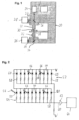
- figure 1 1 shows a scanning microscope 20 having at least one light source 22 .
- the light source 22 generates an illuminating light beam 23 which is focused on a sample 30 via a scanning unit 24 and a beam splitter 26 with the aid of a first lens 28 .
- a first detection beam 31 emanating from the sample in the direction of illumination is directed onto a first detector arrangement 36 via a second lens 32 and a mirror 34 .
- a second detection beam 40 emanating from the sample 30 counter to the direction of illumination is directed via the beam splitter 26 onto a second detector arrangement 38 .
- the detection beams 31 and 40 are not deflected using the scanning unit 24 .
- the first and second detector arrays 36, 38 are therefore also referred to as "non-descanned detectors" (NDD).
- NDD non-descanned detectors
- the scanning microscope 20 can also be referred to as a device comprising a microscope for examining the sample 30 .
- further detection beams can arise, which are fed back via the scanning unit 24 and which are detected using one or more detectors (not shown).
- the scanning microscope 20 can be a confocal scanning microscope.
- the first lens 28 focuses the illuminating light beam 23 onto a focal area on or in the sample 30.
- the focal area is point-shaped.
- the focus area can be designed in the form of a line, for example when using a line scanner.
- a closed scan field is preferably scanned optically.
- the focus area can also be moved in the z-direction perpendicular to the plane.
- the detection beams 31, 40 emanating from the sample 30 arise essentially from fluorescence effects which occur as a result of the illumination of the sample 30. Special effects, such as 2 or more photon effects, can also be used. Microscopy methods in which the devices according to the invention can be used, or effects that can be observed with the assembly 20 are in particular FLIM (Fluorescence Lifetime Imaging), FRAP (Fluorescence Recovery After Photobleaching), FRET (Fluorescence Resonance Energy Transfer) and FCS (Fluorescence Correlation -spectroscopy).
- FLIM Fluorescence Lifetime Imaging
- FRAP Fluorescence Recovery After Photobleaching
- FRET Fluorescence Resonance Energy Transfer
- FCS Fluorescence Correlation -spectroscopy
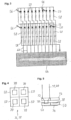
- each of the detector arrangements 36, 38 has two or more photosensitive semiconductor elements 50, as shown in FIG figure 2 shown.
- the photosensitive semiconductor elements 50 thus form the detector arrangements 36, 38, which can each also be referred to as a sensor array or detector array.
- Avalanche photo diodes are used as semiconductor elements 50 . These are operated in Geiger mode above their breakdown voltage. All individual pulses are summed up in analog form for evaluation, so that the overall signal is proportional to the number of incident photons. Alternatively or additionally, the individual pulses can be evaluated directly and counted in the measurement interval.
- the disadvantage that arises from using the avalanche photodiode in the Geiger mode, namely the longer dead time can be compensated for.
- analog summation and direct evaluation can be combined, as in figure 3 shown.
- figure 2 shows a possible circuit according to which the individual semiconductor elements 50 of a detector arrangement 36, 38 can be electrically connected to one another.
- the semiconductor elements 50 are connected in series with one series resistor 58 each, but in parallel with one another.
- the illustrated embodiment of the detector arrangement 36, 38 has a first row 52 and a second row 54 of semiconductor elements 50.
- the parallel-connected semiconductor elements 50 are connected via a single output line 60 to an amplifier 62, which transmits the signals from the semiconductor elements 50 to a common evaluation unit 64 reinforced.
- the evaluation unit 64 adds up the individual detection events in an analogous manner. After each detected event, one of the semiconductor elements 50 has a short dead time during which no new photon 56 can be detected.
- the use of several semiconductor elements 50 connected in parallel reduces the dead time for the entire detector arrangement 36, 38 since one of the semiconductor elements 50 can certainly detect a photon 56 while, for example, an adjacent semiconductor element 50 is currently in its dead time.
- the dead time can be further reduced if an assembly (not shown) is provided for resetting the semiconductor elements 50, the capacitance of the semiconductor elements 50 being resettable passively with the aid of the assembly.
- a separate circuit can be provided which actively resets the capacitance of the semiconductor elements 50 .
- figure 3 shows an alternative circuit of the semiconductor elements 50, in which two of the semiconductor elements 50 are connected in parallel to one another and are connected to the evaluation unit 64 via an output line 60 in each case.
- This circuit makes it possible to detect the individual signals of the two semiconductor elements 50 connected in parallel as a pair independently of the other pairs of semiconductor elements 50 . The detection events can then be summed up analogously and evaluated in pairs.
- the exemplary embodiments shown can easily be combined with one another by any number of semiconductor elements 50 connected in parallel being detected together via a common output 60 .
- the chip structure, in particular the number of outputs 60, can thus be specified in a simple manner.
- the Figures 4 and 5 show an embodiment in top view or side view, in which the quantum yield of the detector arrays 36, 38 is particularly large.
- the sides of the semiconductor elements 50 which face the detection beams 31, 40 have a light-sensitive area 70 which is as large as possible and as closed as possible.
- the fill factor on the light-sensitive surface is as large as possible.
- semiconductor elements 50 are used which are based on back-thinned technology, in which light-insensitive structures 74 of the semiconductor elements 50, for example contacts, are arranged on the side of the corresponding semiconductor element 50 facing away from the detection beams 31, 40.
- the quantum yield is increased further by arranging a lens 72 in front of each light-sensitive region 70 of a semiconductor element 50 .
- the lens 72 focuses the light of the detection light beams 31, 40 onto the light-sensitive area 70 of a semiconductor element 50.
- the individual lenses 72 can also be combined as a unit and are referred to as a lens arrangement or as a microlens array.
- the cooling device can, for example, have Peltier elements, in particular multi-stage Peltier elements.
- the detector arrangements 36, 38 can optionally be arranged in a protective atmosphere.
- the protective atmosphere prevents the formation of condensate on the photosensitive areas 70 of the semiconductor elements 50. This is particularly advantageous for detecting small signals which stand out only slightly or not at all from the dark noise without cooling or a protective atmosphere.
- the detection light beams 31, 40 are coupled into a light guide (not shown) before they are detected.
- a liquid light guide according to the invention is particularly advantageous because, on the one hand, it has relatively good transmission properties and, on the other hand, it can be produced with a relatively large diameter.
- the large diameter makes it easier to image even strongly deflected detection beams 31, 40 reliably onto the cross section of the corresponding light guide and thus onto one of the detector arrangements 36, 38 with approximately no effects on the detection quality.
- the invention is not limited to the specified exemplary embodiments.
- other light-sensitive components can also be used as semiconductor elements 50 for detector arrangements 36, 38.
- only one or more detector arrangements 36, 38 can be arranged.
- different detector arrangements 36, 38 can be provided.
- the scanning microscope can, instead of the scanning unit 24, comprise a scanning table on which the sample 30 is arranged and which moves the sample 30 under the illuminating light beam 23 directed onto the sample 30 and thereby a focal area of the illuminating light beam 23 moved within the predetermined scan field on or in the sample 30.
Landscapes
- Physics & Mathematics (AREA)
- Engineering & Computer Science (AREA)
- Computer Vision & Pattern Recognition (AREA)
- General Engineering & Computer Science (AREA)
- Chemical & Material Sciences (AREA)
- Analytical Chemistry (AREA)
- General Physics & Mathematics (AREA)
- Optics & Photonics (AREA)
- Microscoopes, Condenser (AREA)
Description
- Die Erfindung betrifft eine Vorrichtung zum Untersuchen einer Probe, umfassend ein Mikroskop mit einer Lichtquelle, einer Scaneinheit und mit einem Detektor. Die Lichtquelle erzeugt einen Beleuchtungslichtstrahl. Die Scaneinheit lenkt den über ein Objektiv auf die Probe gelenkten Beleuchtungslichtstrahl ab und bewegt dadurch einen Fokusbereich des Beleuchtungslichtstrahls innerhalb eines vorgegebenen Scanfelds auf oder in der Probe. Der Detektor detektiert einen von der Probe ausgehenden und von der Scaneinheit nicht abgelenkten Detektionslichtstrahl.
- Beim optischen Abtasten der Probe mit einem Scan-Mikroskop wird zu einem vorgegebenen Zeitpunkt ein ausgewählter punktförmiger oder zeilenförmiger Bereich der Probe optisch abgetastet. Dazu fokussiert eine Fokussieroptik, insbesondere ein Objektiv, des Mikroskops den Beleuchtungslichtstrahl auf den ausgewählten Bereich der Probe und detektiert den Anteil des Lichts, der von dem ausgewählten Bereich beispielsweise aufgrund von Fluoreszenzeffekten in der Probe zurückgeworfen wird. Die gewonnenen Bilddaten werden gespeichert. Nachfolgend werden weitere punktförmige bzw. zeilenförmige Bereiche untersucht, die vorzugsweise aneinander grenzen und beispielsweise eine Linie bzw. eine Fläche bilden. Auf diese Weise kann ein großer Bereich der Probe Punkt für Punkt und Zeile für Zeile optisch abgetastet werden. Ferner ist auch eine Abtastung in Richtung parallel zu dem Beleuchtungslichtstrahl möglich, so dass insgesamt ein dreidimensionaler Bereich, insbesondere ein Volumen, abtastbar ist. Die Daten der einzelnen Punkte werden nachfolgend mittels einer Datenverarbeitungsanlage zu einem Gesamtbild des untersuchten Bereichs der Probe zusammengesetzt.
- Bei konfokalen Scan-Mikroskopen werden regelmäßig Detektoren eingesetzt, die allgemein als NDDs (Non-Descanned-Detector) bezeichnet werden, da diese dazu vorgesehen sind, Detektionslichtstrahlen zu detektieren, die auf die Detektoren treffen, ohne über die Scaneinheit rückgeführt zu werden, und somit im Gegensatz zu den Beleuchtungslichtstrahlen nicht von einer Scaneinheit des Scan-Mikroskops abgelenkt werden. NDDs werden bei bekannten Mikroskopen sowohl objektiv- als auch kondensorseitig angebracht, wobei sie im Falle der objektivseitigen Anordnung auch als RLD bzw. bei der kondensorseitigen Anordnung auch als TLD bezeichnet werden. Die detektierten Ereignisse werden für jeden Detektor einzeln oder für alle Detektoren kombiniert ausgewertet. Als photosensitive Bauelemente werden bei bekannten NDDs Fotomultiplier oder EMCCDs (Elektron-Multiplying-CCD) verwendet. Diese erhalten gegenüber anderen photosensitiven Bauelementen den Vorzug, da deren lichtempfindlicher Bereich relativ groß gestaltet werden kann, was nötig ist, da sich aufgrund der Scanbewegung des Beleuchtungslichtstrahls auch der Detektionslichtstrahl auf der photosensitiven Oberfläche des Detektors zumindest geringfügig bewegt und da dies eine minimale Größe des lichtempfindlichen Bereichs des photosensitiven Bauelements von typischerweise 3mm x 3mm erfordert, um Licht von allen Scanpositionen auf den lichtempfindlichen Bereich lenken zu können. Bei dem Detektionslicht handelt es sich insbesondere um von der Probe abgestrahltes Fluoreszenzlicht.
- Zum Detektieren der Detektionsstrahlen, die über den Scanner rückgeführt werden, werden als Lichtdetektoren unter anderen Lawinenfotodioden (Avalanche-Photo-Diodes kurz APDs) verwendet. Diese sind wesentlich empfindlicher als Fotomultiplier. Die maximale Größe des lichtempfindlichen Bereichs einer derartigen Lawinenfotodiode beträgt bei bekannten Lawinenfotodioden jedoch nur ca. 50µm x 50µm.
- Aus dem Dokument
US 2007/206276 A1 ist ein Scanmikroskop mit einem Non-Descanned-Detektor bekannt, bei dem mehrere Probenorte gleichzeitig punktförmig mittels mehrerer Teilstrahlen beleuchtet werden. Zum Abrastern der Probe ist ein Scanspiegel vorhanden, durch den die Auftrefforte der Teilstrahlen auf der Probe simultan verschoben werden können. Die von der Probe ausgehenden Detektionslichtbündel werden zu dem Non-Descanned-Detektor umgelenkt, der eine CCD-Kamera mit einem zweidimensionalen Sensorfeld umfasst. - Es ist Aufgabe der vorliegenden Erfindung, eine Vorrichtung zum Untersuchen einer Probe umfassend ein Mikroskop zu schaffen, die es ermöglicht, nicht über eine Scaneinheit zurückgeführte Detektionsstrahlen mit einer hohen Sensitivität zu detektieren.
- Die Aufgabe wird gelöst durch die Merkmale des Patentanspruchs 1. Vorteilhafte Ausgestaltungen sind in den Unteransprüchen angegeben.
- Die Erfindung zeichnet sich dadurch aus, dass als Detektor eine Detektoranordnung angeordnet ist, die zwei oder mehr photosensitive Halbleiterelemente umfasst. Die Verwendung mehrerer Halbleiterelemente für einen Detektor, insbesondere für die Detektoranordnung ermöglicht, mit der lichtempfindlichen Fläche der photosensitiven Halbleiterelemente einen großen Bereich abzudecken und somit die sich bewegenden Detektionslichtstrahlen in jeder Scanposition zu detektieren. Ferner ermöglicht die Verwendung der photosensitiven Halbleiterelemente eine hohe Detektorempfindlichkeit, insbesondere eine hohe Quanteneffizienz, und eine hohe Zeitauflösung der detektierten Ereignisse. Ferner kann gegenüber bekannten nicht konfokal arbeitenden Mikroskopen, bei denen unter anderem PMT-Röhren als Detektoren verwendet werden, die Baugröße des Mikroskops, insbesondere der Detektoranordnung besonders gering gehalten werden. Dies spielt besonders dann eine wesentliche Rolle, wenn mehrere Detektoren in einem Gerät verwendet werden sollen, beispielsweise zum Detektieren von unterschiedlichen spektralen Bereichen.
- Die Detektoranordnung kann auch als Detektorarray bezeichnet werden. Die Detektoranordnung mit den mehreren photosensitiven Halbleiterelementen kann als einzelnes Bauelement hergestellt werden und in der Vorrichtung eingebaut sein. Ferner kann die Vorrichtung auch mehrere Detektoranordnungen, die jeweils zwei oder mehr photosensitive Halbleiterelemente aufweisen, umfassen. Eines der Halbleiterelemente ist beispielsweise eine Photodiode, insbesondere eine Lawinenfotodiode (APD). Die Halbleiterdioden, insbesondere die Lawinenfotodioden im Geiger-Betrieb setzen für jedes detektierte Photon eine nahezu gleichgroße Elektronenlawine frei, wodurch gegenüber Photomultipliern (PMT) oder verstärkten CCDs eine Rauschquelle entfällt, die dort aus der unterschiedlichen Anzahl frei gesetzter Elektronen resultiert. Ein weiterer Vorteil der APD's im Vergleich zu herkömmlichen PMT's ist, dass diese auch in einem starken Magnetfeld einwandfrei funktionieren. Ferner ist die zeitliche Auflösung bei APD's besser als bei PMT's (z.B. bei FLIM). Somit sind APD's für Einzelphototnen-Messungen (z.B. FCS) besser geeignet als PMT's.
- Die Quanteneffizienz kann weiter erhöht werden, indem entlang des Detektionsstrahlengangs vor, insbesondere unmittelbar vor jedem Halbleiterelement je eine Linse angeordnet ist, die den Detektionslichtstrahl auf das entsprechende Halbleiterelement, insbesondere den photosensitiven Bereich des entsprechenden Halbleiterelements, fokussiert. So kann einfach Detektionslicht, das ohne die Linsen auf einen lichtunempfindlichen Bereich eines oder mehrerer Halbleiterelemente, beispielsweise zwischen zwei der Halbleiterelemente, treffen würde, auf den photosensitiven Bereich eines der angrenzenden Halbleiterelemente fokussiert werden. Dadurch gehen keine Detektionslichtstrahlen verloren. Die einzelnen Linsen können auch als Einheit zusammengefasst sein und/oder als Mikrolinsenarray bezeichnet werden.
- Ein Verringern der Totzeit zwischen zwei detektierbaren Ereignissen und ein Erhöhen der Dynamik der Detektoranordnung wird dadurch erreicht, dass zumindest zwei der Halbleiterelemente parallel geschaltet sind. Ferner kann so ein Ausgang der Detektoranordnung mehreren parallel angeordneten Halbleiterelementen oder parallelen Reihen von Halbleiterelementen zugeordnet werden. Dies trägt dazu bei, die Struktur der Detektoranordnung zu optimieren.
- Die Quanteneffizienz wir in einer vorteilhaften Ausgestaltung weiter erhöht, indem lichtunempfindliche Strukturen der Halbleiterelemente auf einer von dem Detektionslichtstrahl abgewandten Seite der Halbleiterelemente angeordnet sind. Diese besondere Anordnung der lichtunempfindlichen Strukturen wird regelmäßig auch als "back-thinned" oder "backilluminated technology" bezeichnet. Diese Technologie ermöglicht, eine Photonendetektionswahrscheinlichkeit von über 80 % pro Halbleiterelement zu erzielen.
- Aufgrund der hohen Photonendetektionswahrscheinlichkeit und dem günstigen Rauschverhalten ist die Sensitivität der Detektoranordnung gegenüber bekannten Detektoren für nicht konfokal arbeitende Scan-Mikroskope besonders hoch. Ferner hat die Detektoranordnung bei vorgegebener Beleuchtungsstärke ein besonders gutes Signal-RauschVerhältnis.
- Die Detektoranordnung mit den photosensitiven Halbleiterelementen kann auch bei einem konfokalen Mikroskop mit einem Scantisch verwendet werden.
- Ausführungsbeispiele der Erfindung sind im Folgenden anhand von schematischen Zeichnungen näher erläutert.
- Es zeigen:
- Figur 1
- ein Scan-Mikroskop,
- Figur 2
- ein Schaltbild einer ersten Ausführungsform einer Detektoranordnung,
- Figur 3
- ein Schaltbild einer zweiten Ausführungsform der Detektoranordnung,
- Figur 4
- eine Draufsicht auf eine dritte Ausführungsform Detektoranordnung, und
- Figur 5
- eine Seitenansicht der dritten Ausführungsform der Detektoranordnung.
- Elemente gleicher Konstruktion oder Funktion sind figurenübergreifend mit den gleichen Bezugszeichen gekennzeichnet.
-
Figur 1 zeigt ein Scan-Mikroskop 20, das zumindest eine Lichtquelle 22 hat. Die Lichtquelle 22 erzeugt einen Beleuchtungslichtstrahl 23, der über eine Scaneinheit 24 und einen Strahlteiler 26 mit Hilfe eines ersten Objektivs 28 auf eine Probe 30 fokussiert wird. Ein von der Probe in Beleuchtungsrichtung ausgehender erster Detektionsstrahl 31 wird über ein zweites Objektiv 32 und einen Spiegel 34 auf eine erste Detektoranordnung 36 gelenkt. Ein von der Probe 30 entgegen der Beleuchtungsrichtung ausgehender zweiter Detektionsstrahl 40 wird über den Strahlteiler 26 auf eine zweite Detektoranordnung 38 gelenkt. Die Detektionsstrahlen 31 und 40 werden nicht mit Hilfe der Scaneinheit 24 abgelenkt. Die erste und zweite Detektoranordnung 36, 38 werden daher auch als "Non-Descanned-Detektoren" (NDD) bezeichnet. Das Scan-Mikroskop 20 kann auch als Vorrichtung umfassend ein Mikroskop zum Untersuchen der Probe 30 bezeichnet werden. Zusätzlich zu den Detektionsstrahlen 31 und 40 können weitere Detektionsstrahlen entstehen, die über die Scaneinheit 24 zurückgeführt werden und die mit Hilfe eines oder mehrerer nicht dargestellten Detektoren detektiert werden. Somit kann das Scan-Mikroskop 20 ein konfokales Scan-Mikroskop sein. - Das erste Objektiv 28 fokussiert den Beleuchtungslichtstrahl 23 auf einen Fokusbereich auf oder in der Probe 30. Der Fokusbereich ist punktförmig ausgebildet. Alternativ dazu kann der Fokusbereich linienförmig ausgebildet sein, beispielsweise bei Verwendung eines Zeilenscanners. Beim Scannen der Probe 30 wird der Fokusbereich in x- und y-Richtung innerhalb einer Ebene bewegt, die senkrecht auf dem Beleuchtungslichtstrahl 23 steht. Dabei wird vorzugsweise ein geschlossenes Scanfeld optisch abgetastet. Bereich Zusätzlich kann der Fokusbereich auch in z-Richtung senkrecht zu der Ebene bewegt werden.
- Die von der Probe 30 ausgehenden Detektionsstrahlen 31, 40 entstehen im Wesentlichen aus Fluoreszenzeffekten, die infolge der Beleuchtung der Probe 30 auftreten. Dabei können auch spezielle Effekte, wie beispielsweise 2- oder Mehr-Photoneneffekte. Mikroskopieverfahren, bei denen die erfindungsgemäßen Vorrichtungen anwendbar sind, oder dabei auftretende mit der Baueinheit 20 zu beobachtende Effekte sind insbesondere FLIM (Fluoreszenz Lifetime Imaging), FRAP (Fluorescence Recovery After Photobleaching), FRET (Fluoreszenz Resonanz Energie Transfer) und FCS (Fluoreszenz-Korrelations-Spektroskopie).
- Da der Beleuchtungslichtstrahl 23 durch die Scaneinheit 24 abgelenkt wird, die Detektionslichtstrahlen 31 und 40 jedoch nicht konfokal rückgeführt werden und daher auch deren Strahlverlauf nicht durch die Scaneinheit 24 korrigiert wird, werden auch die Detektionslichtstrahlen 31 und 40 auf einer Oberfläche der ersten und zweiten Detektoranordnung 36, 38 bewegt. Damit die Detektionslichtstrahlen 31, 40 in jeder Scanposition der Scaneinheit 24 zuverlässig detektiert werden können, weist jede der Detektoranordnungen 36, 38 jeweils zwei oder mehr photosensitive Halbleiterelemente 50 auf, wie in
Figur 2 gezeigt. Somit bilden die photosensitiven Halbleiterelemente 50 die Detektoranordnungen 36, 38, die jeweils auch als Sensorarray oder Detektorarray bezeichnet werden können. - Als Halbleiterelemente 50 werden Lawinenfotodioden (Avalanche-Photo-Diods, APD) verwendet. Diese werden oberhalb ihrer Durchbruchspannung im Geigermodus betrieben. Zum Auswerten werden alle Einzelimpulse analog aufsummiert, so dass das Gesamtsignal proportional zur Anzahl der einfallenden Photonen ist. Alternativ oder zusätzlich können die Einzelimpulse direkt ausgewertet und im Messinterval gezählt werden. Durch die Verwendung mehrerer Lawinenfotodioden kann der Nachteil, der durch Verwendung der Lawinenfotodiode im Geigermodus entsteht, nämlich die längere Totzeit, kompensiert werden. Ferner können Analog-Summation und Direkt-Auswertung kombiniert werden, wie in
Figur 3 gezeigt. -
Figur 2 zeigt eine mögliche Schaltung, gemäß der die einzelnen Halbleiterelemente 50 einer Detektoranordnung 36, 38 miteinander elektrisch verbunden sein können. Dabei sind die Halbleiterelemente 50 in Reihe mit je einem Vorwiderstand 58 jedoch parallel zueinander geschaltet. Insbesondere hat die dargestellte Ausführungsform der Detektoranordnung 36, 38 eine erste Reihe 52 und eine zweite Reihe 54 von Halbleiterelementen 50. Die parallel geschalteten Halbleiterelemente 50 liegen über eine einzige Ausgangsleitung 60 an einem Verstärker 62 an, der die Signale der Halbleiterelemente 50 für eine gemeinsame Auswerteeinheit 64 verstärkt. Die Auswerteeinheit 64 summiert die einzelnen Detektionsereignisse analog auf. Nach jedem detektierten Ereignis hat eines der Halbleiterelemente 50 eine kurze Totzeit, während der kein neues Photon 56 detektiert werden kann. Die Verwendung mehrerer Halbleiterelemente 50, die parallel geschaltet sind, verringert für die gesamte Detektoranordnung 36, 38 die Totzeit, da je eines der Halbleiterelemente 50 durchaus ein Photon 56 detektieren kann, während beispielsweise ein benachbartes Halbleiterelement 50 sich gerade in seiner Totzeit befindet. - Die Totzeit kann weiter verringert werden, wenn eine Baugruppe (nicht dargestellt) zum Zurücksetzen der Halbleiterelemente 50 vorgesehen ist, wobei die Kapazität der Halbleiterelemente 50 passiv mit Hilfe der Baugruppe zurücksetzbar ist. Alternativ oder zusätzlich dazu kann eine eigene Schaltung vorgesehen sein, die die Kapazität der Halbleiterelemente 50 aktiv zurücksetzt.
-
Figur 3 zeigt eine alternative Schaltung der Halbleiterelemente 50, bei der jeweils zwei der Halbleiterelemente 50 parallel zueinander geschaltet sind und über jeweils eine Ausgangsleitung 60 mit der Auswerteeinheit 64 verbunden sind. Diese Schaltung ermöglicht, jeweils die Einzelsignale der beiden parallel geschalteten Halbleiterelemente 50 als Paar unabhängig von den anderen Paaren der Halbleiterelemente 50 zu erfassen. Die Detektionsereignisse können dann analog aufsummiert und paarweise ausgewertet werden. - Die in
Figur 2 undFigur 3 gezeigten Ausführungsbeispiele können einfach miteinander kombiniert werden, indem jeweils eine beliebige Anzahl von parallel geschalteten Halbleiterelementen 50 über einen gemeinsamen Ausgang 60 zusammen erfasst werden. So kann einfach die Chipstruktur, insbesondere die Anzahl der Ausgänge 60 vorgegeben werden. - Die
Figuren 4 und 5 zeigen ein Ausführungsbeispiel in Draufsicht bzw. Seitenansicht, bei dem die Quantenausbeute der Detektoranordnungen 36, 38 besonders groß ist. Dabei weisen die Seiten der Halbleiterelemente 50, die den Detektionsstrahlen 31, 40 zugewandt sind, einen möglichst großen, möglichst geschlossenen lichtempfindlichen Bereich 70 auf. In anderen Worten ist der Füllfaktor an lichtempfindlicher Fläche möglichst groß. Dies wird zum Einen dadurch erzielt, dass die photosensitiven Halbleiterelemente 50 möglichst lückenfrei aneinander anschließen. Zum Anderen werden dabei Halbleiterelemente 50 verwendet, die auf der back-thinned Technologie basieren, bei welcher lichtunempfindliche Strukturen 74 der Halbleiterelemente 50, beispielsweise Kontakte, auf der von den Detektionsstrahlen 31, 40 abgewandten Seite des entsprechenden Halbleiterelements 50 angeordnet sind. Die Quantenausbeute wird weiter erhöht, indem vor jedem lichtempfindlichen Bereich 70 eines Halbleiterelements 50 je eine Linse 72 angeordnet ist. Die Linse 72 fokussiert das Licht der Detektionslichtstrahlen 31, 40 auf den lichtempfindlichen Bereich 70 je eines Halbleiterelements 50. Die einzelnen Linsen 72 können auch als Einheit zusammengefasst werden und als Linsenanordnung oder als Mikrolinsenarray bezeichnet werden. - Ein Dunkelrauschen einer oder beider Detektoranordnungen 36, 38 wird besonders gering gehalten, indem die entsprechende Detektoranordnung 36, 38 thermisch mit einer Kühlvorrichtung gekoppelt und dadurch gekühlt wird. Die Kühlvorrichtung kann beispielsweise Peltier-Elemente, insbesondere mehrstufige Peltier-Elemente aufweisen. Darüber hinaus können die Detektoranordnungen 36, 38 optional in einer Schutzatmosphäre angeordnet sein. Die Schutzatmosphäre verhindert das Entstehen von Kondensat an den photosensitiven Bereichen 70 der Halbleiterelemente 50. Dies ist besonders zum Detektieren kleiner Signale, die sich ohne Kühlung oder Schutzatmosphäre nur geringfügig oder gar nicht vom Dunkelrauschen abheben, vorteilhaft.
- Die Detektionslichtstrahlen 31, 40 werden in einen Lichtleiter (nicht dargestellt) eingekoppelt, bevor sie detektiert werden. Dabei ist die erfindungsgemäße Verwendung eines Flüssiglichtleiters besonders vorteilhaft, da er zum Einen relativ gute Transmissionseigenschaften aufweist und da er zum Anderen mit einem relativ großen Durchmesser hergestellt werden kann. Der große Durchmesser erleichtert es, auch stark abgelenkte Detektionsstrahlen 31, 40 sicher auf den Querschnitt des entsprechenden Lichtleiters und so mit näherungsweise keinen Auswirkungen auf die Detektionsqualität auf eine der Detektoranordnungen 36, 38 abzubilden.
- Die Erfindung ist nicht auf die angegebenen Ausführungsbeispiele beschränkt. Beispielsweise können als Halbleiterelemente 50 auch andere lichtempfindliche Bauelemente für die Detektoranordnungen 36, 38 verwendet werden. Ferner können lediglich eine oder weitere Detektoranordnungen 36, 38 angeordnet sein. Beispielsweise können zum Detektieren von unterschiedlichen spektralen Bereichen der Detektionsstrahlen 31, 40 jeweils unterschiedliche Detektoranordnungen 36, 38 vorgesehen sein. In einer nicht unter die Ansprüche fallenden Alternative kann das Scan-Mikroskop anstatt der Scaneinheit 24 einen Scantisch umfassen, auf dem die Probe 30 angeordnet ist und der die Probe 30 unter dem auf die Probe 30 gelenkten Beleuchtungslichtstrahl 23 bewegt und dadurch einen Fokusbereich des Beleuchtungslichtstrahls 23 innerhalb des vorgegebenen Scanfelds auf oder in der Probe 30 bewegt.
-
- 20
- Scan-Mikroskop
- 22
- Lichtquelle
- 23
- Beleuchtungslichtstrahl
- 24
- Scaneinheit
- 26
- Strahlteiler
- 28
- erstes Objektiv
- 30
- Probe
- 31
- erster Detektionsstrahl
- 32
- zweites Objektiv
- 34
- Spiegel
- 36
- erste Detektoranordnung
- 38
- zweite Detektoranordnung
- 40
- zweiter Detektionsstrahl
- 50
- Halbleiterelement
- 52
- erste Reihe
- 54
- zweite Reihe
- 56
- Lawinenphotodiode
- 58
- Vorwiderstand
- 60
- Ausgang
- 62
- Verstärker
- 64
- Auswerteeinheit
- 70
- lichtempfindlicher Bereich
- 72
- Linse
- 75
- lichtunempfindlicher Bereich
Claims (5)
- Vorrichtung zum Untersuchen einer Probe (30), umfassendein Mikroskop,mit einer Lichtquelle (22), die einen Beleuchtungslichtstrahl (23) erzeugt, einer Scaneinheit (24), die den über ein Objektiv auf die Probe (30) gelenkten Beleuchtungslichtstrahl (23) ablenkt und dadurch einen Fokusbereich des Beleuchtungslichtstrahls (23) innerhalb eines vorgegebenen Scanfelds auf oder in der Probe (30) bewegt,und mit mindestens einer Detektoranordnung (36), die zwei oder mehr photosensitive Halbleiterelemente (50) umfasst und die einen von der Probe (30) ausgehenden und von der Scaneinheit (24) nicht abgelenkten Detektions-Lichtstrahl (31, 40) detektiert,wobei die Vorrichtung dadurch gekennzeichnet, dass zumindest zwei Halbleiterelemente (50) elektrisch parallel geschaltet und über eine gemeinsame Ausgangsleitung (60) mit einer Auswerteeinheit (64) verbunden sind, wobei die Halbleiterelemente (50) jeweils eine Lawinenfotodiode aufweisen, die oberhalb ihrer Durchbruchspannung im Geigermodus betrieben wird, unddass der Detektionsstrahlengang über einen Flüssiglichtleiter verläuft.
- Vorrichtung nach Anspruch 1, bei der entlang des Detektionsstrahlengangs (40) vor jedem Halbleiterelement (50) je eine Linse (72) angeordnet ist, die den Detektions-Lichtstrahl (31, 40) auf das entsprechende Halbleiterelement (50) fokussiert.
- Vorrichtung nach einem der vorstehenden Ansprüche, bei der lichtunempfindliche Strukturen (74) der Halbleiterelemente (50) auf einer von dem Detektions-Lichtstrahl (31, 40) abgewandten Seite der Halbleiterelemente (50) angeordnet sind.
- Vorrichtung nach einem der vorstehenden Ansprüche, bei der die Detektoranordnung (36) in einer Schutzatmosphäre angeordnet und/oder thermisch mit einer Kühleinheit gekoppelt ist.
- Vorrichtung nach einem der vorstehenden Ansprüche, mit einer Baugruppe zum Zurücksetzen der Halbleiterelemente (50), die die Kapazität der Halbleiterelemente (50) passiv oder aktiv zurücksetzt.
Applications Claiming Priority (1)
| Application Number | Priority Date | Filing Date | Title |
|---|---|---|---|
| DE102009057304.6A DE102009057304B4 (de) | 2009-12-07 | 2009-12-07 | Vorrichtung zum Untersuchen einer Probe umfassend ein Mikroskop |
Publications (3)
| Publication Number | Publication Date |
|---|---|
| EP2336817A1 EP2336817A1 (de) | 2011-06-22 |
| EP2336817B1 EP2336817B1 (de) | 2020-06-17 |
| EP2336817B2 true EP2336817B2 (de) | 2023-08-16 |
Family
ID=43638773
Family Applications (1)
| Application Number | Title | Priority Date | Filing Date |
|---|---|---|---|
| EP10193888.4A Active EP2336817B2 (de) | 2009-12-07 | 2010-12-07 | Vorrichtung zum Untersuchen einer Probe umfassend ein Mikroskop |
Country Status (2)
| Country | Link |
|---|---|
| EP (1) | EP2336817B2 (de) |
| DE (1) | DE102009057304B4 (de) |
Family Cites Families (9)
| Publication number | Priority date | Publication date | Assignee | Title |
|---|---|---|---|---|
| US6134002A (en) * | 1999-01-14 | 2000-10-17 | Duke University | Apparatus and method for the rapid spectral resolution of confocal images |
| US6734415B1 (en) * | 1999-10-07 | 2004-05-11 | Agilent Technologies, Inc. | High quantum efficiency point light detector |
| DE10253609A1 (de) * | 2002-11-15 | 2004-05-27 | Leica Microsystems Heidelberg Gmbh | Scanmikroskop |
| CN1839417A (zh) * | 2003-08-22 | 2006-09-27 | 纳幕尔杜邦公司 | 利用透明发光聚合物验证身份的方法 |
| DE102005059948A1 (de) * | 2005-01-31 | 2006-08-03 | Leica Microsystems Cms Gmbh | Detektor |
| US7329860B2 (en) * | 2005-11-23 | 2008-02-12 | Illumina, Inc. | Confocal imaging methods and apparatus |
| US7619732B2 (en) * | 2006-03-01 | 2009-11-17 | Leica Microsystems Cms Gmbh | Method and microscope for high spatial resolution examination of samples |
| US7990524B2 (en) * | 2006-06-30 | 2011-08-02 | The University Of Chicago | Stochastic scanning apparatus using multiphoton multifocal source |
| DE102007024074B4 (de) * | 2007-05-22 | 2022-09-15 | Leica Microsystems Cms Gmbh | Mikroskop |
-
2009
- 2009-12-07 DE DE102009057304.6A patent/DE102009057304B4/de active Active
-
2010
- 2010-12-07 EP EP10193888.4A patent/EP2336817B2/de active Active
Non-Patent Citations (6)
| Title |
|---|
| "Handbook of Biological Confocal Microscopy. 3rd Ed.", 1 January 2006, article PAWLEY JAMES B.: "Multi-Photon", pages: 447, 535 - 542 † |
| A.G. STEWART ET AL: "Properties of silicon photon counting detectors and silicon photomultipliers", JOURNAL OF MODERN OPTICS, vol. 56, no. 2-3, 20 January 2009 (2009-01-20), pages 240 - 252 † |
| GRIGORIEV, E. ET AL: "Silicon photomultipliers and their bio-medical applications", NUCLEAR INSTRUMENTS & METHODS IN PHYSICS RESEARCH. SECTION A, vol. 571, no. 1-2, 26 January 2007 (2007-01-26), pages 130 - 133 † |
| HAMAMATSU PHOTONICS - CATALOGUE: "MPPC Multi-Pixel Photon Counter", HAMAMATSU PHOTONICS - CATALOGUE, 1 January 2007 (2007-01-01), pages 1 - 16 † |
| N OTTE: "The Silicon Photomultiplier -A new device for High Energy Physics, Astroparticle Physics, Industrial and Medical Applications", SNIC SYMPOSIUM, STANFORD, CALIFORNIA, 3 April 2006 (2006-04-03), pages 1 - 9 † |
| WOKOSIN D.L., AMOS W.B., WHITE J.G.: "Detection sensitivity enhancements for fluorescence imaging with multi-photon excitation microscopy", ENGINEERING IN MEDICINE AND BIOLOGY SOCIETY,1998. PROCEEDINGS OF THE20TH ANNUAL INTERNATIONAL CONFERENCE OF THE IEEE, vol. 4, 29 October 1998 (1998-10-29) - 1 November 1998 (1998-11-01), pages 1707 - 1714 † |
Also Published As
| Publication number | Publication date |
|---|---|
| DE102009057304B4 (de) | 2025-01-23 |
| EP2336817A1 (de) | 2011-06-22 |
| EP2336817B1 (de) | 2020-06-17 |
| DE102009057304A1 (de) | 2011-06-09 |
Similar Documents
| Publication | Publication Date | Title |
|---|---|---|
| EP3526634B1 (de) | Optikgruppe für detektionslicht für ein mikroskop, verfahren zur mikroskopie und mikroskop | |
| EP2149037B1 (de) | Vorrichtung zur lichtdetektion in einem scanmikroskop | |
| EP3857588B1 (de) | Verfahren zum betreiben eines vielstrahl-teilchenstrahlmikroskops | |
| EP2546621B1 (de) | Vorrichtung und Verfahren zum Detektieren von Licht | |
| EP0898783A2 (de) | Rastermikroskop, bei dem eine probe in mehreren probenpunkten gkeichzeitig optisch angeregt wird | |
| DE102020209889A1 (de) | Mikroskop und Verfahren zur mikroskopischen Bildaufnahme mit variabler Beleuchtung | |
| DE3340647A1 (de) | Verfahren zur fokussierung eines mikroskopes sowie mikroskop zur durchfuehrung des verfahrens | |
| EP1664889B1 (de) | Vorrichtung zum nachweis von photonen eines lichtstrahls | |
| DE102013005927B4 (de) | Verfahren zum optisch hochaufgelösten Rasterscanning eines Objekts und Verwendung des Verfahrens | |
| DE102010055882A1 (de) | Pinhole für ein konfokales Laser-Scanning Mikroskop | |
| DE102004003993A1 (de) | Vorrichtung zum Nachweis von Photonen eines Lichtstrahls | |
| DE102023100926A1 (de) | Mikroskop | |
| EP2336817B2 (de) | Vorrichtung zum Untersuchen einer Probe umfassend ein Mikroskop | |
| WO2018188693A1 (de) | Monozentrische empfangsanordnung | |
| DE10017824B4 (de) | Vorrichtung zur parallelen photometrischen Fluoreszenz- oder Lumineszenzanalyse mehrerer voneinander getrennter Probenbereiche auf einem Objekt | |
| WO2012069220A1 (de) | Vorrichtung zum messen einer ladungsträgerlebensdauer in einem halbleitersubstrat | |
| EP2271961A1 (de) | Verfahren zum kalibrieren einer ablenkeinheit in einem tirf-mikroskop, tirf-mikroskop und verfahren zu dessen betrieb | |
| DE19707225A1 (de) | Lichtabtastvorrichtung | |
| DE10206004A1 (de) | Vorrichtung zur konfokalen optischen Mikroanalyse | |
| DE102020202804A1 (de) | Verfahren und Vorrichtung zur Bilderfassung | |
| EP1803157B1 (de) | Emccd-detektor sowie ein spektrometer und mikroskop | |
| EP1691180A2 (de) | Detektor mit Mikrolinsen-Anordnung | |
| EP1929256A1 (de) | Photosensor-chip, laser-mikroskop mit photosensor-chip und verfahren zum auslesen eines photosensor-chips | |
| DE10200264B4 (de) | Lichtsondenmikroskop | |
| DE102023132199A1 (de) | Chromatisch-konfokale Messvorrichtung und Verfahren zur Messung des Abstands zu einem Objekt |
Legal Events
| Date | Code | Title | Description |
|---|---|---|---|
| PUAI | Public reference made under article 153(3) epc to a published international application that has entered the european phase |
Free format text: ORIGINAL CODE: 0009012 |
|
| AK | Designated contracting states |
Kind code of ref document: A1 Designated state(s): AL AT BE BG CH CY CZ DE DK EE ES FI FR GB GR HR HU IE IS IT LI LT LU LV MC MK MT NL NO PL PT RO RS SE SI SK SM TR |
|
| AX | Request for extension of the european patent |
Extension state: BA ME |
|
| 17P | Request for examination filed |
Effective date: 20111222 |
|
| STAA | Information on the status of an ep patent application or granted ep patent |
Free format text: STATUS: EXAMINATION IS IN PROGRESS |
|
| 17Q | First examination report despatched |
Effective date: 20170313 |
|
| GRAP | Despatch of communication of intention to grant a patent |
Free format text: ORIGINAL CODE: EPIDOSNIGR1 |
|
| STAA | Information on the status of an ep patent application or granted ep patent |
Free format text: STATUS: GRANT OF PATENT IS INTENDED |
|
| INTG | Intention to grant announced |
Effective date: 20191216 |
|
| GRAS | Grant fee paid |
Free format text: ORIGINAL CODE: EPIDOSNIGR3 |
|
| GRAJ | Information related to disapproval of communication of intention to grant by the applicant or resumption of examination proceedings by the epo deleted |
Free format text: ORIGINAL CODE: EPIDOSDIGR1 |
|
| GRAL | Information related to payment of fee for publishing/printing deleted |
Free format text: ORIGINAL CODE: EPIDOSDIGR3 |
|
| STAA | Information on the status of an ep patent application or granted ep patent |
Free format text: STATUS: EXAMINATION IS IN PROGRESS |
|
| GRAR | Information related to intention to grant a patent recorded |
Free format text: ORIGINAL CODE: EPIDOSNIGR71 |
|
| STAA | Information on the status of an ep patent application or granted ep patent |
Free format text: STATUS: GRANT OF PATENT IS INTENDED |
|
| GRAA | (expected) grant |
Free format text: ORIGINAL CODE: 0009210 |
|
| STAA | Information on the status of an ep patent application or granted ep patent |
Free format text: STATUS: THE PATENT HAS BEEN GRANTED |
|
| INTC | Intention to grant announced (deleted) | ||
| AK | Designated contracting states |
Kind code of ref document: B1 Designated state(s): AL AT BE BG CH CY CZ DE DK EE ES FI FR GB GR HR HU IE IS IT LI LT LU LV MC MK MT NL NO PL PT RO RS SE SI SK SM TR |
|
| INTG | Intention to grant announced |
Effective date: 20200511 |
|
| REG | Reference to a national code |
Ref country code: GB Ref legal event code: FG4D Free format text: NOT ENGLISH |
|
| REG | Reference to a national code |
Ref country code: CH Ref legal event code: EP |
|
| REG | Reference to a national code |
Ref country code: DE Ref legal event code: R096 Ref document number: 502010016668 Country of ref document: DE |
|
| REG | Reference to a national code |
Ref country code: IE Ref legal event code: FG4D Free format text: LANGUAGE OF EP DOCUMENT: GERMAN |
|
| REG | Reference to a national code |
Ref country code: AT Ref legal event code: REF Ref document number: 1282033 Country of ref document: AT Kind code of ref document: T Effective date: 20200715 |
|
| PG25 | Lapsed in a contracting state [announced via postgrant information from national office to epo] |
Ref country code: FI Free format text: LAPSE BECAUSE OF FAILURE TO SUBMIT A TRANSLATION OF THE DESCRIPTION OR TO PAY THE FEE WITHIN THE PRESCRIBED TIME-LIMIT Effective date: 20200617 Ref country code: SE Free format text: LAPSE BECAUSE OF FAILURE TO SUBMIT A TRANSLATION OF THE DESCRIPTION OR TO PAY THE FEE WITHIN THE PRESCRIBED TIME-LIMIT Effective date: 20200617 Ref country code: LT Free format text: LAPSE BECAUSE OF FAILURE TO SUBMIT A TRANSLATION OF THE DESCRIPTION OR TO PAY THE FEE WITHIN THE PRESCRIBED TIME-LIMIT Effective date: 20200617 Ref country code: NO Free format text: LAPSE BECAUSE OF FAILURE TO SUBMIT A TRANSLATION OF THE DESCRIPTION OR TO PAY THE FEE WITHIN THE PRESCRIBED TIME-LIMIT Effective date: 20200917 Ref country code: GR Free format text: LAPSE BECAUSE OF FAILURE TO SUBMIT A TRANSLATION OF THE DESCRIPTION OR TO PAY THE FEE WITHIN THE PRESCRIBED TIME-LIMIT Effective date: 20200918 |
|
| REG | Reference to a national code |
Ref country code: LT Ref legal event code: MG4D |
|
| REG | Reference to a national code |
Ref country code: NL Ref legal event code: MP Effective date: 20200617 |
|
| PG25 | Lapsed in a contracting state [announced via postgrant information from national office to epo] |
Ref country code: RS Free format text: LAPSE BECAUSE OF FAILURE TO SUBMIT A TRANSLATION OF THE DESCRIPTION OR TO PAY THE FEE WITHIN THE PRESCRIBED TIME-LIMIT Effective date: 20200617 Ref country code: LV Free format text: LAPSE BECAUSE OF FAILURE TO SUBMIT A TRANSLATION OF THE DESCRIPTION OR TO PAY THE FEE WITHIN THE PRESCRIBED TIME-LIMIT Effective date: 20200617 Ref country code: HR Free format text: LAPSE BECAUSE OF FAILURE TO SUBMIT A TRANSLATION OF THE DESCRIPTION OR TO PAY THE FEE WITHIN THE PRESCRIBED TIME-LIMIT Effective date: 20200617 Ref country code: BG Free format text: LAPSE BECAUSE OF FAILURE TO SUBMIT A TRANSLATION OF THE DESCRIPTION OR TO PAY THE FEE WITHIN THE PRESCRIBED TIME-LIMIT Effective date: 20200917 |
|
| PG25 | Lapsed in a contracting state [announced via postgrant information from national office to epo] |
Ref country code: NL Free format text: LAPSE BECAUSE OF FAILURE TO SUBMIT A TRANSLATION OF THE DESCRIPTION OR TO PAY THE FEE WITHIN THE PRESCRIBED TIME-LIMIT Effective date: 20200617 Ref country code: AL Free format text: LAPSE BECAUSE OF FAILURE TO SUBMIT A TRANSLATION OF THE DESCRIPTION OR TO PAY THE FEE WITHIN THE PRESCRIBED TIME-LIMIT Effective date: 20200617 |
|
| PG25 | Lapsed in a contracting state [announced via postgrant information from national office to epo] |
Ref country code: SM Free format text: LAPSE BECAUSE OF FAILURE TO SUBMIT A TRANSLATION OF THE DESCRIPTION OR TO PAY THE FEE WITHIN THE PRESCRIBED TIME-LIMIT Effective date: 20200617 Ref country code: EE Free format text: LAPSE BECAUSE OF FAILURE TO SUBMIT A TRANSLATION OF THE DESCRIPTION OR TO PAY THE FEE WITHIN THE PRESCRIBED TIME-LIMIT Effective date: 20200617 Ref country code: CZ Free format text: LAPSE BECAUSE OF FAILURE TO SUBMIT A TRANSLATION OF THE DESCRIPTION OR TO PAY THE FEE WITHIN THE PRESCRIBED TIME-LIMIT Effective date: 20200617 Ref country code: IT Free format text: LAPSE BECAUSE OF FAILURE TO SUBMIT A TRANSLATION OF THE DESCRIPTION OR TO PAY THE FEE WITHIN THE PRESCRIBED TIME-LIMIT Effective date: 20200617 Ref country code: RO Free format text: LAPSE BECAUSE OF FAILURE TO SUBMIT A TRANSLATION OF THE DESCRIPTION OR TO PAY THE FEE WITHIN THE PRESCRIBED TIME-LIMIT Effective date: 20200617 Ref country code: ES Free format text: LAPSE BECAUSE OF FAILURE TO SUBMIT A TRANSLATION OF THE DESCRIPTION OR TO PAY THE FEE WITHIN THE PRESCRIBED TIME-LIMIT Effective date: 20200617 Ref country code: PT Free format text: LAPSE BECAUSE OF FAILURE TO SUBMIT A TRANSLATION OF THE DESCRIPTION OR TO PAY THE FEE WITHIN THE PRESCRIBED TIME-LIMIT Effective date: 20201019 |
|
| PG25 | Lapsed in a contracting state [announced via postgrant information from national office to epo] |
Ref country code: IS Free format text: LAPSE BECAUSE OF FAILURE TO SUBMIT A TRANSLATION OF THE DESCRIPTION OR TO PAY THE FEE WITHIN THE PRESCRIBED TIME-LIMIT Effective date: 20201017 Ref country code: PL Free format text: LAPSE BECAUSE OF FAILURE TO SUBMIT A TRANSLATION OF THE DESCRIPTION OR TO PAY THE FEE WITHIN THE PRESCRIBED TIME-LIMIT Effective date: 20200617 Ref country code: SK Free format text: LAPSE BECAUSE OF FAILURE TO SUBMIT A TRANSLATION OF THE DESCRIPTION OR TO PAY THE FEE WITHIN THE PRESCRIBED TIME-LIMIT Effective date: 20200617 |
|
| REG | Reference to a national code |
Ref country code: DE Ref legal event code: R026 Ref document number: 502010016668 Country of ref document: DE |
|
| PLBI | Opposition filed |
Free format text: ORIGINAL CODE: 0009260 |
|
| 26 | Opposition filed |
Opponent name: CARL ZEISS MICROSCOPY GMBH Effective date: 20210317 |
|
| PG25 | Lapsed in a contracting state [announced via postgrant information from national office to epo] |
Ref country code: DK Free format text: LAPSE BECAUSE OF FAILURE TO SUBMIT A TRANSLATION OF THE DESCRIPTION OR TO PAY THE FEE WITHIN THE PRESCRIBED TIME-LIMIT Effective date: 20200617 |
|
| PG25 | Lapsed in a contracting state [announced via postgrant information from national office to epo] |
Ref country code: SI Free format text: LAPSE BECAUSE OF FAILURE TO SUBMIT A TRANSLATION OF THE DESCRIPTION OR TO PAY THE FEE WITHIN THE PRESCRIBED TIME-LIMIT Effective date: 20200617 |
|
| PLAX | Notice of opposition and request to file observation + time limit sent |
Free format text: ORIGINAL CODE: EPIDOSNOBS2 |
|
| REG | Reference to a national code |
Ref country code: CH Ref legal event code: PL |
|
| PG25 | Lapsed in a contracting state [announced via postgrant information from national office to epo] |
Ref country code: MC Free format text: LAPSE BECAUSE OF FAILURE TO SUBMIT A TRANSLATION OF THE DESCRIPTION OR TO PAY THE FEE WITHIN THE PRESCRIBED TIME-LIMIT Effective date: 20200617 |
|
| REG | Reference to a national code |
Ref country code: BE Ref legal event code: MM Effective date: 20201231 |
|
| PLBB | Reply of patent proprietor to notice(s) of opposition received |
Free format text: ORIGINAL CODE: EPIDOSNOBS3 |
|
| PG25 | Lapsed in a contracting state [announced via postgrant information from national office to epo] |
Ref country code: LU Free format text: LAPSE BECAUSE OF NON-PAYMENT OF DUE FEES Effective date: 20201207 Ref country code: IE Free format text: LAPSE BECAUSE OF NON-PAYMENT OF DUE FEES Effective date: 20201207 |
|
| PG25 | Lapsed in a contracting state [announced via postgrant information from national office to epo] |
Ref country code: LI Free format text: LAPSE BECAUSE OF NON-PAYMENT OF DUE FEES Effective date: 20201231 Ref country code: CH Free format text: LAPSE BECAUSE OF NON-PAYMENT OF DUE FEES Effective date: 20201231 |
|
| REG | Reference to a national code |
Ref country code: AT Ref legal event code: MM01 Ref document number: 1282033 Country of ref document: AT Kind code of ref document: T Effective date: 20201207 |
|
| PG25 | Lapsed in a contracting state [announced via postgrant information from national office to epo] |
Ref country code: AT Free format text: LAPSE BECAUSE OF NON-PAYMENT OF DUE FEES Effective date: 20201207 |
|
| PG25 | Lapsed in a contracting state [announced via postgrant information from national office to epo] |
Ref country code: TR Free format text: LAPSE BECAUSE OF FAILURE TO SUBMIT A TRANSLATION OF THE DESCRIPTION OR TO PAY THE FEE WITHIN THE PRESCRIBED TIME-LIMIT Effective date: 20200617 Ref country code: MT Free format text: LAPSE BECAUSE OF FAILURE TO SUBMIT A TRANSLATION OF THE DESCRIPTION OR TO PAY THE FEE WITHIN THE PRESCRIBED TIME-LIMIT Effective date: 20200617 Ref country code: CY Free format text: LAPSE BECAUSE OF FAILURE TO SUBMIT A TRANSLATION OF THE DESCRIPTION OR TO PAY THE FEE WITHIN THE PRESCRIBED TIME-LIMIT Effective date: 20200617 |
|
| PG25 | Lapsed in a contracting state [announced via postgrant information from national office to epo] |
Ref country code: MK Free format text: LAPSE BECAUSE OF FAILURE TO SUBMIT A TRANSLATION OF THE DESCRIPTION OR TO PAY THE FEE WITHIN THE PRESCRIBED TIME-LIMIT Effective date: 20200617 |
|
| PG25 | Lapsed in a contracting state [announced via postgrant information from national office to epo] |
Ref country code: BE Free format text: LAPSE BECAUSE OF NON-PAYMENT OF DUE FEES Effective date: 20201231 |
|
| PLAB | Opposition data, opponent's data or that of the opponent's representative modified |
Free format text: ORIGINAL CODE: 0009299OPPO |
|
| R26 | Opposition filed (corrected) |
Opponent name: CARL ZEISS MICROSCOPY GMBH Effective date: 20210317 |
|
| P01 | Opt-out of the competence of the unified patent court (upc) registered |
Effective date: 20230414 |
|
| PUAH | Patent maintained in amended form |
Free format text: ORIGINAL CODE: 0009272 |
|
| STAA | Information on the status of an ep patent application or granted ep patent |
Free format text: STATUS: PATENT MAINTAINED AS AMENDED |
|
| 27A | Patent maintained in amended form |
Effective date: 20230816 |
|
| AK | Designated contracting states |
Kind code of ref document: B2 Designated state(s): AL AT BE BG CH CY CZ DE DK EE ES FI FR GB GR HR HU IE IS IT LI LT LU LV MC MK MT NL NO PL PT RO RS SE SI SK SM TR |
|
| REG | Reference to a national code |
Ref country code: DE Ref legal event code: R102 Ref document number: 502010016668 Country of ref document: DE |
|
| PGFP | Annual fee paid to national office [announced via postgrant information from national office to epo] |
Ref country code: GB Payment date: 20241217 Year of fee payment: 15 |
|
| PGFP | Annual fee paid to national office [announced via postgrant information from national office to epo] |
Ref country code: FR Payment date: 20241227 Year of fee payment: 15 |
|
| PGFP | Annual fee paid to national office [announced via postgrant information from national office to epo] |
Ref country code: DE Payment date: 20241227 Year of fee payment: 15 |