EP2333599A1 - Imaging unit and imaging device - Google Patents
Imaging unit and imaging device Download PDFInfo
- Publication number
- EP2333599A1 EP2333599A1 EP09817674A EP09817674A EP2333599A1 EP 2333599 A1 EP2333599 A1 EP 2333599A1 EP 09817674 A EP09817674 A EP 09817674A EP 09817674 A EP09817674 A EP 09817674A EP 2333599 A1 EP2333599 A1 EP 2333599A1
- Authority
- EP
- European Patent Office
- Prior art keywords
- layer
- image capturing
- capturing element
- lens
- actuator
- Prior art date
- Legal status (The legal status is an assumption and is not a legal conclusion. Google has not performed a legal analysis and makes no representation as to the accuracy of the status listed.)
- Withdrawn
Links
Images








Classifications
-
- H—ELECTRICITY
- H10—SEMICONDUCTOR DEVICES; ELECTRIC SOLID-STATE DEVICES NOT OTHERWISE PROVIDED FOR
- H10F—INORGANIC SEMICONDUCTOR DEVICES SENSITIVE TO INFRARED RADIATION, LIGHT, ELECTROMAGNETIC RADIATION OF SHORTER WAVELENGTH OR CORPUSCULAR RADIATION
- H10F39/00—Integrated devices, or assemblies of multiple devices, comprising at least one element covered by group H10F30/00, e.g. radiation detectors comprising photodiode arrays
- H10F39/80—Constructional details of image sensors
- H10F39/806—Optical elements or arrangements associated with the image sensors
-
- G—PHYSICS
- G02—OPTICS
- G02B—OPTICAL ELEMENTS, SYSTEMS OR APPARATUS
- G02B13/00—Optical objectives specially designed for the purposes specified below
- G02B13/001—Miniaturised objectives for electronic devices, e.g. portable telephones, webcams, PDAs, small digital cameras
- G02B13/0015—Miniaturised objectives for electronic devices, e.g. portable telephones, webcams, PDAs, small digital cameras characterised by the lens design
- G02B13/002—Miniaturised objectives for electronic devices, e.g. portable telephones, webcams, PDAs, small digital cameras characterised by the lens design having at least one aspherical surface
- G02B13/004—Miniaturised objectives for electronic devices, e.g. portable telephones, webcams, PDAs, small digital cameras characterised by the lens design having at least one aspherical surface having four lenses
-
- G—PHYSICS
- G02—OPTICS
- G02B—OPTICAL ELEMENTS, SYSTEMS OR APPARATUS
- G02B13/00—Optical objectives specially designed for the purposes specified below
- G02B13/001—Miniaturised objectives for electronic devices, e.g. portable telephones, webcams, PDAs, small digital cameras
- G02B13/0055—Miniaturised objectives for electronic devices, e.g. portable telephones, webcams, PDAs, small digital cameras employing a special optical element
- G02B13/006—Miniaturised objectives for electronic devices, e.g. portable telephones, webcams, PDAs, small digital cameras employing a special optical element at least one element being a compound optical element, e.g. cemented elements
-
- G—PHYSICS
- G02—OPTICS
- G02B—OPTICAL ELEMENTS, SYSTEMS OR APPARATUS
- G02B7/00—Mountings, adjusting means, or light-tight connections, for optical elements
- G02B7/02—Mountings, adjusting means, or light-tight connections, for optical elements for lenses
-
- G—PHYSICS
- G03—PHOTOGRAPHY; CINEMATOGRAPHY; ANALOGOUS TECHNIQUES USING WAVES OTHER THAN OPTICAL WAVES; ELECTROGRAPHY; HOLOGRAPHY
- G03B—APPARATUS OR ARRANGEMENTS FOR TAKING PHOTOGRAPHS OR FOR PROJECTING OR VIEWING THEM; APPARATUS OR ARRANGEMENTS EMPLOYING ANALOGOUS TECHNIQUES USING WAVES OTHER THAN OPTICAL WAVES; ACCESSORIES THEREFOR
- G03B3/00—Focusing arrangements of general interest for cameras, projectors or printers
- G03B3/10—Power-operated focusing
-
- H—ELECTRICITY
- H04—ELECTRIC COMMUNICATION TECHNIQUE
- H04N—PICTORIAL COMMUNICATION, e.g. TELEVISION
- H04N23/00—Cameras or camera modules comprising electronic image sensors; Control thereof
- H04N23/50—Constructional details
- H04N23/55—Optical parts specially adapted for electronic image sensors; Mounting thereof
-
- H—ELECTRICITY
- H10—SEMICONDUCTOR DEVICES; ELECTRIC SOLID-STATE DEVICES NOT OTHERWISE PROVIDED FOR
- H10F—INORGANIC SEMICONDUCTOR DEVICES SENSITIVE TO INFRARED RADIATION, LIGHT, ELECTROMAGNETIC RADIATION OF SHORTER WAVELENGTH OR CORPUSCULAR RADIATION
- H10F39/00—Integrated devices, or assemblies of multiple devices, comprising at least one element covered by group H10F30/00, e.g. radiation detectors comprising photodiode arrays
- H10F39/80—Constructional details of image sensors
- H10F39/804—Containers or encapsulations
Definitions
- the present invention relates to a compact imaging unit and an imaging device.
- a camera module is generally installed on a compact electronic device such as a mobile telephone, and the camera module has been demanded to be made smaller.
- this camera module requires, for example, a lens barrel and a lens holder which support the lens, a holder which supports an infrared (IR) cut filter, a housing that holds a laminated body made up of a substrate, an image capturing element, and an optical element, a resin which seals the laminated body, and the like. Therefore, when the above multiple parts are made smaller, it has not been easy to make a camera module by precisely combining the multiple parts.
- IR infrared
- a technique is proposed in which a substrate, a semiconductor sheet formed with multiple image capturing elements and a lens array sheet formed with multiple image capturing lenses are attached with resin layers interposed therebetween to form a laminated member, and the laminated member is subjected to dicing, to complete individual camera modules (e.g., Patent Document 1, etc). Further, a technique is also proposed in which an image sensor wafer formed by arranging a plurality of image sensor chips in a matrix state, a lens array formed by integrating a plurality of lenses, an IR filter glass, and a diaphragm film are integrally attached in this order to form a structure and the structure is cut along the boundary of the image sensor chips, to complete individual camera modules (e.g., Patent Document 2, etc).
- the present invention has been made in view of the above problem, and it is an object of the present invention to provide a technique of enabling both of higher functionality and higher accuracy in a compact optical system.
- an imaging unit includes a laminated structure formed by laminating a plurality of layers including: an image capturing element layer including an image capturing element part; a lens layer capable of changing a distance from the image capturing element layer; and an actuator layer including a movable part for moving the lens layer; and a signal transmitter disposed so as to connect the actuator layer and the image capturing element layer and transmitting a drive signal for driving the movable part from the image capturing element layer side to the actuator layer.
- the actuator layer is interposed between the image capturing element layer and the lens layer.
- An imaging unit is the imaging unit according to the first aspect, wherein the laminated structure further includes another lens layer which is arranged on an opposite side of the image capturing element layer with respect to the lens layer, with a fixed distance from the image capturing element part.
- An imaging unit is the imaging unit according to the first aspect, wherein the laminated structure further includes one or more function layers which are interposed between the image capturing element layer and the actuator layer, and the signal transmitter penetrates through the function layers.
- An imaging unit is the imaging unit according to the first aspect, wherein the laminated structure further includes one or more function layers which are interposed between the image capturing element layer and the actuator layer, and the signal transmitter is disposed along outer rims of the function layers.
- An imaging unit is the imaging unit according to the first aspect, wherein the movable part includes a film element which is reversibly deformed according to the drive signal, and moves the lens layer by means of deformation of the film element.
- An imaging unit is the imaging unit according to the fifth aspect, wherein the movable part includes, as the film element, a thin film of a shape memory alloy attached to a substrate.
- An imaging unit is the imaging unit according to the fifth aspect, wherein the movable part includes, as the film element, a thin film of a piezoelectric element attached to a substrate.
- An imaging device has an imaging unit.
- the imaging unit includes a laminated structure formed by laminating a plurality of layers including; an image capturing element layer including an image capturing element part; a lens layer capable of changing a distance from the image capturing element layer; and an actuator layer including a movable part for moving the lens layer; and a signal transmitter disposed so as to connect the actuator layer and the image capturing element layer and transmitting a drive signal for driving the movable part from the image capturing element layer side to the actuator layer, in which the actuator layer is interposed between the image capturing element layer and the lens layer.
- the imaging unit receives a supply of the drive signal to drive the lens layer.
- the imaging unit according to any of the first to seventh aspects can shorten a signal transmitter which transmits the drive signal to the actuator, so that it is possible to realize a more reliable driving mechanism which achieves higher functionality in a compact imaging unit such as an imaging unit made at a wafer level.
- the imaging unit according to the second aspect can improve lens performance in the compact imaging unit while maintaining high reliability.
- imaging unit when imaging units including a compact driving mechanism are manufactured, by providing similar penetrating wiring parts in other sheets which are laminated and bonded to an actuator layer, it is possible to readily and precisely form a signal transmitter for applying an electrical field to a movable part.
- FIG. 1 is a schematic view illustrating a schematic configuration of a mobile telephone 100 on which a camera module 500A according to an embodiment of the present invention is installed. Note that, FIG. 1 and subsequent figures are adequately assigned three X, Y and Z axes orthogonal to each other to clarify an azimuth relationship.
- the mobile telephone 100 is formed as a folding mobile telephone, and has a first housing 200, a second housing 300 and a hinge part 400.
- the first housing 200 and the second housing 300 are each a plate rectangular parallelepiped, and function as housings which accommodate various electronic members. More specifically, the first housing 200 has a camera module 500A and a variable display (not illustrated), and the second housing 300 has a controller which electrically controls the mobile telephone 100 and an operating member (not illustrated) such as buttons.
- the hinge part 400 pivotally connects the first housing 200 and the second housing 300. By this means, the mobile telephone 100 is made foldable.
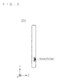
- FIG. 2 is a schematic sectional view focusing on the first housing 200 of the mobile telephone 100.
- the camera module 500A is a compact imaging device, that is, a micro camera unit (MCU), having a size of about 5 square mm in an X-Y cross section and a thickness (depth in the Z direction) of the order of about 3 mm.
- MCU micro camera unit
- the configuration of the camera module 500A and its manufacturing steps will be described below in order.
- FIG. 3 is a schematic sectional view of the camera module 500A where a direction indicated by an arrow YJ1 is a +Z direction.
- the camera module 500A has a driving mechanism KB which drives a lens 16 of a photo-taking optical system and an image capturer PB which acquires an image captured from an object image.
- the image capturer PB has a configuration in which, for example, an image capturing element layer 11 which has an image capturing element 111 such as a COMS sensor or a CCD sensor, an image capturing element holder layer 12, and an infrared (IR) cut filter layer 13 are laminated in this order.
- an image capturing element layer 11 which has an image capturing element 111 such as a COMS sensor or a CCD sensor
- an image capturing element holder layer 12 an image capturing element holder layer 12
- an infrared (IR) cut filter layer 13 are laminated in this order.
- a lens layer 16 In space covered by the image capturer PB and a cover 20 which allows incidence of light from a ceiling surface by, for example, adopting a structure having an opening part in the ceiling surface, are stored a lens layer 16, a first parallel spring (lower layer parallel spring) 15 and a second parallel spring (upper layer parallel spring) 17 which hold the lens layer 16, and a actuator layer (driving layer) 14 which functions as a driver, all of which are made in a wafer state (at a wafer level).
- the respective function layers stored in this space form the driving mechanism KB which drives the lens layer 16 in cooperation with each other.
- the cover 20 and the image capturer PB serve as a fixing part with respect to the lens layer 16.
- the lens layer 16 is supported by the first parallel spring 15 and the second parallel spring 17 bonded to the fixing part. More specifically, the first parallel spring 15 is interposed between the image capturer PB and the lens layer 16 on the one principal plane side (-Z side) of the lens layer 16, and the second parallel spring 17 is interposed between the cover 20 and lens layer 16 on the other principal plane side (+Z side) of the lens layer 16.
- the first parallel spring 15 and the second parallel spring 17 are each elastically deformed, and the lens layer 16 rests in a position where the elastic force of the first parallel spring 15 and the elastic force of the second parallel spring 17 balance out.
- the actuator layer 14 has an actuator which produces driving displacement in the direction (+Z direction) from the one principal plane side of the lens layer 16 to the other principal plane side, and is arranged on one principal plane side (the lower surface side in the illustrated example) of the lens layer 16 (more specifically, each of lens G1 to G3 of FIG. 6 forming the lens layer 16) and on the other principal plane side (upper surface side in the illustrated example of FIG. 3 ) of the image capturing element layer 11. That is, the actuator layer 14 is interposed between the image capturing element layer 11 and the lens layer 16, and there is no lens element between the actuator layer 14 and the image capturing element layer 11.
- the actuator contacts projecting parts 161 projecting toward the one principal plane side of the lens layer 16, and driving displacement produced in the actuator is transmitted to the lens layer 16 through the projecting parts 161.
- An outer rim wiring part CT1A (CT2A) is disposed from the image capturing element layer 11 to the actuator layer 14 along the outer rims of the image capturing element holder layer 12 and the infrared (IR) cut filter layer 13, and functions as a signal transmitter which transmits a drive signal for driving the actuator, from a predetermined electrode pad provided in the image capturing element layer 11 which holds the image capturing element layer 11 to the actuator layer 14.
- the camera module 500A has a laminated structure LS laminating a plurality of layers 11, 12, 13, 14, 15, 16 and 17, and the lens layer 16 which is a driven body is bonded to elastic members arranged in positions to oppose each other across the lens layer 16 and the elastic members hold the lens layer 16 in a state of being elastically deformed toward each other in a direction vertical to the lens layer 16 (vertical direction of the lens layer 16). Then, the lens layer 16 receives the driving force from the actuator of the actuator layer 14 interposed between the image capturing element layer 11 and the lens layer 16, and is displaced from its position.
- the driving mechanism KB provided in the camera module 500A can displace the lens layer 16 made at a wafer level, in the optical axis direction of the lens layer 16, and makes the camera module 500A function as an imaging device having the lens driving function.
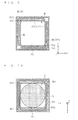
- FIG. 4 is a view illustrating an upper surface external view of the image capturing element layer 11 to which the image capturing element 111 is attached
- FIG. 5 is a schematic sectional view of the image capturing element layer 11 seen from a cross-sectional line 11A-11A of FIG. 4 .
- the image capturing element layer 11 is a member which has the image capturing element 111 which generates an image signal of an object image by receiving light of the object having passed through the photo-taking optical system, its peripheral circuit C11, and an outer peripheral part F11 surrounding the peripheral circuit C11. Note that, on the surface on the one principal plane side of the image capturing element layer 11 (the lower surface side in the illustrated example of FIG. 3 ), solder balls HB used for soldering according to a reflow scheme are provided.
- electrode pads T11a and T11b are formed on the surface on the other principal plane side of the image capturing element layer 11 (the upper surface side in the illustrated example of FIG. 5 ).
- the electrode pads T11a and T11b are each electrically connected with outer rim electrodes CT1A and CT2A illustrated in FIG. 3 in the periphery of the image capturing element layer 11.
- penetrating electrodes L11a and L11b penetrating through the image capturing element layer 11 are formed on the one principal plane side of the electrode pad T11a (the lower surface side in the illustrated example of FIG. 5 ).
- One end of the penetrating electrode L11a is electrically connected with the electrode pad T11a, and the other end is electrically connected with one solder ball HB provided in the surface on the one principal plane side of the image capturing element layer 11 (lower surface side in the illustrated example of FIG. 5 ).
- one end of the penetrating electrode L11b is electrically connected with the electrode pad T11b, and the other end is electrically connected with one of solder balls HB to which the penetrating electrode L11a is not electrically connected.
- the solder balls HB are electrically connected with an electronic circuit inside the mobile telephone 100.
- the voltage (drive signals) for driving the actuator layer 14 of the camera module 500A is generated inside the mobile telephone 100, and then is supplied to the actuator layer 14 through wirings or electrodes of the penetrating electrodes L11a and L11b and outer rim electrodes CT1A and CT2A of the image capturing element layer 11.
- various terminals for connecting wirings for giving signals to the image capturing element 111 and reading signals from the image capturing element 111 are provided on the surface on the other principal plane side of the image capturing element layer 11 (upper surface side in the illustrated example of FIG. 5 ).
- the image capturing element holder layer 12 is a member which is made of, for example, a material such as resin and which holds the image capturing element layer 11 bonded by, for example, an adhesive. An opening is provided at about the center of the image capturing element holder layer 12.
- the infrared cut filter layer 13 is formed by layering transparent thin films of different refractive indices on a transparent substrate.
- the infrared cut filter layer 13 is formed by, for example, spattering multiple transparent thin films of different refractive indices on the upper surface of the substrate made of a glass or transparent resin, and controls a waveband of transmitting light by means of the combination of the thickness and refractive index of the thin film.
- the infrared cut filter layer 13, which blocks light of the waveband of 600 nm or more, is adopted.
- the lens layer 16 is made at a wafer level using a glass substrate as a base material, and is molded by, for example, overlapping two or more lenses. A case will be illustrated with the present embodiment where the lens layer 16 is formed by overlapping three lenses.
- FIG. 6 is a schematic sectional view of the lens layer 16 where a direction indicated by an arrow YJ2 is a +Z direction.
- FIG. 7 is a lower surface external view of the lens layer 16.
- the lens layer 16 has a lens constituting layer LY1 with a first lens G1, a lens constituting layer LY2 with a second lens G2, and a lens constituting layer LY3 with a third lens G3, and the respective lens constituting layers LY1 to LY3 are bonded in this order with ribs RB interposed therebetween.
- projecting parts 161 in a non-lens part which does not function as a lens are provided on one principal plane of the lens constituting layer LY1 with the first lens G1.
- FIG. 8 is a view illustrating how the lens constituting layer LY3 with the third lens G3 is made.
- an acrylic or epoxy ultraviolet (UV) cured resin of high transparency is applied to both surfaces of the glass substrate 160. Then, both surfaces are pressed by transparent lens shaping molds 162 having a shape of each lens (third lens G3 in FIG. 8 ) at a predetermined pressure and are radiated by ultraviolet rays UV1, so that polymer lenses GP1 and GP2 are each formed on the respective surfaces of the glass substrate 160.
- UV ultraviolet
- each of the lens constituting layers LY1 to LY3 made in this way alignment marks for positioning are formed in two or more predetermined positions.
- the respective lens constituting layers LY 1 to LY3 are built up as the integrated lens layer 16 with rib layers having the ribs RB, between each of the lens constituting layers LY1 to LY3.
- each of the lens constituting layers LY1 to LY3 and the rib layers are aligned and bonded keeping a substrate shape as is by using a mask aligner and checking respective alignment marks.
- a bonding method adopts a method of providing a UV cured layer in the rib layer surface to be bonded to each of the lens constituting layers LY1 to LY3 and bonding the layers by the radiation of ultraviolet rays, or a method (surface activated bonding) of radiating a plasma of inert gas on the rib layer surface and attaching and bonding the rib layer surface keeping the rib layer surface activated.
- a method of applying a shadow mask to the layer with the second lens G2 and then forming a light blocking material thin film a method of forming a diaphragm layer using, for example, a resin material colored additionally by black, or the like is used.
- FIG. 9 is an upper surface external view of the first parallel spring 15.
- FIG. 10 is a view illustrating the first parallel spring 15 attached to the lens layer 16.
- the first parallel spring 15 is an elastic member which has a fixed frame part 151 and an elastic part 152, and makes a layer (elastic layer) which forms a spring mechanism.
- the fixed frame part 151 forms an outer peripheral part of the first parallel spring 15, and bonded to the adjacent actuator layer 14 (more specifically, the frame part F14 (described later) of the actuator layer 14).
- the elastic part 152 has a connecting part PG1 with the fixed frame part 151 and a bonding part PG2 to the lens layer 16, and the connecting part PG1 and the bonding part PG2 are connected through a plate member EB.
- the first parallel spring 15 is bonded to the adjacent actuator layer 14 in the fixed frame part 151. Further, as illustrated in FIG. 10 , the first parallel spring 15 is bonded to the lens layer 16 in the bonding part PG2 provided in the elastic part 152.
- the positions of the connecting part PG1 and the bonding part PG2 are misaligned in the Z direction and the plate member EB is curved causing bending deformation (flexural deformation).
- the first parallel spring 15 functions as a spring mechanism in a state where elastic deformation is produced in the plate member EB.
- the first parallel spring 15 is made using, for example, a SUS metal material or a phosphorus bronze.
- the shape of the parallel spring is patterned on a metal material using photolithography, is immersed in a ferric chloride etching solution and is subjected to wet etching to form the pattern of the parallel spring.
- the actuator layer 14 is a thin plate member in which a displacing element (also referred to as "actuator element") which generates the driving force is provided on the substrate such as a metal or silicon (Si).
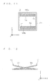
- FIG. 11 is a view illustrating an upper surface external view of the actuator layer 14.
- FIG. 12 is a view illustrating a lateral surface external view of the actuator layer.
- the actuator layer 14 has a frame part F14 forming the outer peripheral part and two plate actuators 14a and 14b provided to project from the frame part F14 toward a hollow part inside the frame part F14. Then, thin film displacing elements (actuator elements) 145a and 145b are provided on the other principal plane sides of the actuators 14a and 14b.
- a shape memory alloy (SMA) is used for the displacing elements 145a and 145b.
- SMA shape memory alloy
- the actuators part 14a and 14b are set in the mold of a shape which needs to be memorized, and are subjected to heating processing (shape memorizing processing) at a predetermined temperature (for example, 600°C).
- the SMA has characteristics that, when the SMA is heated and reaches a predetermined temperature, the SMA is restored to a predetermined shape memorized in advance (also referred to as "memorized shape").
- a predetermined shape memorized in advance also referred to as "memorized shape”
- warped shapes made by free tips FT of the actuators 14a and 14b which are displaced in the +Z direction are memorized. Therefore, when the SMA is heated by conduction of the heater layer, the SMA is contracted and deformed into the memorized shape, and the free tips FT of the actuators 14a and 14b move in the +Z direction (see FIG. 12 ). That is, the free tip FT sides of the actuators 14a and 14b function as displacement transmission parts.
- FIG. 13 is a view for describing the detailed configuration of the actuator layer 14.
- the actuator layer 14 is formed by laminating a first insulation layer 142 illustrated in FIG. 13(b) , a heater layer 143 illustrated in FIG. 13(c) , a second insulation layer 144 illustrated in FIG.13(d) , and a displacing element layer 145 illustrated in FIG. 13(e) in this order on a base layer 141 illustrated in FIG. 13(a) .
- the heater layer 143 illustrated in FIG. 13(c) is shown by being disposed on the first insulation layer 142 for ease of understanding the relationship between positions of wirings etc.
- the base layer 141 is made of, for example, a material having adequate rigidity (for example, silicon), and is formed with a plate base member having a frame part F141 and beam parts 141a and 141b.
- the frame part F141 is a part bonded and fixed to the infrared cut filter layer 13.
- the beam part 141a is a plate-like and arm-shaped part provided to project from one predetermined part the frame part F141
- the beam part 141b is a plate-like and arm-shaped part provided to project from the other predetermined part of the frame part F141.
- the beam parts 141a and 141b are made deformable such that the other end is displaced with the vicinity of one end fixed to the frame part F141 being a fulcrum. Note that, although the frame part F141 and the beam parts 141a and 141b are integrally formed here, the beam parts 141a and 141b are not limited to this and, for example, may be fixed by being fixed to the frame part F141.
- each one end of the beam parts 141a and 141b are fixed to the frame part F141 to serve as a fixed end, and each other end of the beam parts 141a and 141b serves a free tip, and the frame part F141 is formed to surround the beam parts 141a and 141b.
- the first insulation layer 142 is made of, for example, a non-conductive material such as a SiO2 thin film of a predetermined thickness formed by, for example, thermal oxidation, across the entire area of the upper surface of the base layer 141 (surface on the +Z side), and has the same shape as the base layer 141. Accordingly, the first insulation layer 142 has a film frame part F142 formed on the upper surface of the frame part F141, and beam parts 142a and 142b formed on the respective upper surfaces of the beam parts 141a and 141b.
- the frame part F14 of the actuator layer 14 is formed with the frame parts F141, F142 and F144 ( FIG. 13(d) ) laminated mainly upward and downward.
- the heater layer 143 has two thin film resistors 143a and 143b, four electrode parts T1aA, T2aA, T1bA and T2bA and wiring parts CLaA and CLbA.
- the thin film resistor 143a is provided on the beam parts 141a and 142a, and is formed with a thin film resistor which generates heat by being applied the voltage. That is, the beam parts 141a and 142a function here as supporting parts which support thin film resistor 143a. Further, the thin film resistor 143b has the same shape as the thin film resistor 143a, and is formed with a thin film resistor which is provided on the beam parts 141b and 142b and which generates heat by being applied the voltage. That is, the beam parts 141b and 142b function here as supporting parts which support the thin film resistor 143b.
- the thin film resistors 143a and 143b are, for example, formed by spattering, form a photoresist using photolithography and are formed in a predetermined pattern (for example, U-shape) by performing etching of reactive ion etching of thin films formed using this photoresist as an etching mask.
- a thin film resistor extended thinly in a foil shape is formed by bonding by an adhesive etc or bonding by pressure.
- the film forming method may be depositing etc.
- the electrode part T1aA is a part which is made of, for example, a highly conductive metal, which is electrically connected with one end part of the thin film resistor 143a, the outer rim wiring part CT1A illustrated in FIG. 14(b) and the wiring part CLaA, and which applies the voltage supplied through the outer rim wiring part CT1A, to the thin film resistor 143a.
- the electrode part T2aA is a part which is made of, for example, a highly conductive metal similar to the electrode part T1aA, which is electrically connected with the other end part of the thin film resistor 143a, the outer rim wiring part CT2A illustrated in FIG. 14(b) and wiring part CLbA, and which, for example, grounds the other end part of the thin film resistor 143a through the outer rim wiring part CT2A.
- the electrode part T1bA is also a part which is made of, for example, a highly conductive metal, which is electrically connected with one end part of the thin film resistor 143b and wiring part CLaA, and which applies the voltage supplied through the outer rim wiring part CT1A, to the thin film resistor 143b.
- the electrode part T2bA is a part which is made of, for example, a highly conductive metal similar to the electrode part T1bA, which is electrically connected with the other end part of the thin film resistor 143b and the wiring part CLbA, and which, for example, grounds the other end part of the thin film resistor 143b.
- the current flows between the thin film resistors 143a and 143b and the thin film resistors 143a and 143b generate heat by Joule heat.
- the second insulation layer 144 is made of a non-conductive material, and has the same shape as the first insulation layer 142.
- This second insulation layer 144 is formed across, for example, the upper surface of the first insulation layer 142 (the surface on the +Z side) and the entire area of the heater layer 143. Therefore, the second insulation layer 144 insulates the heater layer 143 in cooperation with the first insulation layer 142, and transmits heat generated by the heater layer 143 to the displacing element layer 145 illustrated in FIG. 13(e) .
- the second insulation layer 144 has a film frame part F144 formed on the upper surface of the frame part F142, and beam parts 144a and 144b formed on respective upper surfaces of the beam parts 142a and 142b.
- the second insulation layer 144 is preferably a material which has insulation property and good thermal conductivity, and is formed by forming a film by, for example, spattering aluminum nitride (AIN) or alumina (AI203).
- the displacing element layer 145 has two displacing elements 145a and 145b.
- the displacing elements 145a and 145b are formed with thin film elements (shape memory alloy) which deform according to the rise in the temperature.
- the displacing elements 145a and 145b are formed by, for example, forming a film by spattering, or by bonding by an adhesive etc or bonding by pressure the elements extended thinly in a foil shape.
- the film forming method may be plating, depositing, or the like.
- thermal processing memory thermal processing for memorizing a shape which warps in a concave shape in the +Z direction upon heating is adequately applied to the displacing element 145a and 145b.
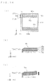
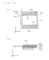
- FIG. 14 is a view for describing the operation of the actuator 14a.
- FIG. 14(a) is a plan view illustrating the configuration of the actuator layer 14 similar to FIG. 11
- FIGS. 14(b) and 14(c) are schematic sectional views focusing on the actuator 14a seen from a cross-sectional line 6A-6A of FIG. 14(a) .
- the current flows to the thin film resistor 143a and the thin film resistor 143a generates heat by Joule heat.
- FIG. 14(b) illustrates a state (initial state) where the actuator 14a is not deformed.
- the initial state the voltage is not applied between the electrodes T1aA and T2aA, and the thin film resistor 143a of the heater layer 143 is at a normal temperature. Therefore, the elastic force of the beam part 141a of the base layer 141 makes the actuator 14a show virtually a flat shape.
- the actuator 14a functions as a driver which generates the driving force by being applied the electric field and deforming such that the free tips are displaced with the place contacting the frame part F14 being a fulcrum. Then, the actuator 14a abuts directly or indirectly on a moving target object, and applies an external force to the moving target object and moves this moving target object.
- the two thin film resistors 143a and 143b are electrically connected with the electrode parts T1aA, T2aA, T1bA, and T2bA through the wiring parts CLaA and CLbA, and are conducted and heated at the same time. Therefore, the two actuator 14a and 14b are deformed almost likewise at almost the same timing with almost the same mechanism.
- the frame part F14 of the actuator layer 14 is bonded to the fixed frame part 151 of the first parallel spring 15 (see FIG. 10 ).
- the free tip FT sides of the actuators 14a and 14b each contact the corresponding projecting parts 161, and displacement produced in the free tips FT of the actuators 14a and 14b is transmitted to the lens layer 16 through each projecting part 161.
- the actuators 14a and 14b function as a functioning part which transmits displacement to the lens layer 16.
- the amount displacement produced at the free tips FT sides of the actuators 14a and 14b varies according to the heating temperature of the SMA, and the amount of displacement can be adjusted by controlling the amount of conduction with the heater layer 143.
- the heater layer 143 is deformed accompanying the deformation of the SMA, the electrical resistance of the heater layer 143 changes accompanying this deformation. Therefore, the amount of displacement may be controlled by monitoring the electrical resistance value of the heater layer 143.
- these displacing elements 145a and 145b function as a film element which can deform reversibly according to a drive signal, and can move the lens layer 16 by means of deformation of this film element.
- the second parallel spring 17 is an elastic member which has the same configuration and function as the first parallel spring 15, and has a fixed frame part 171 and an elastic part 172.
- the fixed frame part 171 of the second parallel spring 17 is bonded to the cover 20, and a bonding part PG2 provided in the elastic part 172 is bonded to the other principal plane of the lens layer 16.
- the plate member EB elastically deforms and the second parallel spring 17 functions as a spring mechanism.
- the cover 20 is molded by press working using a mold by using a resin material as a material.
- the cover 20 protects the driving mechanism KB and serves as a fixing part with respect to the driven body (lens layer 10).
- a plurality of the covers 20 molded in a grid pattern in a resin material are each subjected to dicing for each one of the camera modules 500A.
- FIG. 15 is a flowchart illustrating the manufacturing steps of the camera modules 500A.
- step A preparation of sheets (step SP1),
- step E) securing of driving space (step SP5) are performed sequentially to manufacture the camera modules 500A.
- step A preparation of sheets (step SP1),
- step C) dicing step SP3,
- step D attachment of the cover 20 (step SP4) and
- step E) securing of driving space step SP5
- step SP1 sheets related to each function layer forming the camera module 500A is formed per layer.
- FIG. 16 is a plan view illustrating a configuration of sheets to be prepared. Note that, here, the disc-shaped sheets are prepared.
- each function layer In a sheet of each function layer, multiple chips corresponding to a member related to each function layer are formed in a matrix state in predetermined alignment.
- predetermined alignment is used to include a state where multiple chips are aligned in a predetermined direction at a predetermined interval.
- the image capturing element holder sheet HU2 is made by, for example, press working using a metal mold by using a resin material as a material.
- a base plate is formed in which multiple base layers 141 ( FIG. 13(a) ) are formed in predetermined alignment (here, predetermined alignment in a matrix state).
- the base layers 141 may be formed with a thin plate made of polyimide and the like.
- the insulation film is formed on the base plate using, for example, a photolithographic method or thermal oxidation method, and the first insulation layer 142 ( FIG. 13(b) ) is formed on each base layer 141.
- the heater layer 143 ( FIG. 13(c) ) is formed using, for example a spattering method (or depositing method).
- the thin film resistors 143a and 143b electrode parts T1aA, T2aA, T1bA, and T2bA and wiring parts CLaA and CLbA are formed.
- the electrode parts T1aA and T2aA are preferably subjected to dicing and then formed in the positions reaching the periphery parts of individual actuator layers.
- the second insulation layer 144 ( FIG. 13(d) ) is formed by forming a thin film which has insulation property and, preferably, good thermal conductivity, by using, for example, the spattering method (or depositing method).
- the displacing element layer 145 ( FIG. 13(e) ) is formed using, for example, the spattering method (or depositing method). At this time, the displacing elements 145a and 145b are formed. Then, the actuators 14a and 14b are set in a mold of a shape which needs to be memorized, and are subjected to heating processing (shape memorizing processing) at a predetermined temperature (for example, 600°C).
- step SP1 similar to the image capturing element holder sheet HU2, each of the sheets HU1 and HU3 to HU7 including chips related to each function layer of the image capturing element layer 11, infrared cut filter layer 13, actuator layer 14, first parallel spring 15, lens layer 16, and second parallel spring 17 is prepared.
- FIG. 17 is a view schematically illustrating how the prepared sheets HU1 to HU7 are sequentially laminated and bonded.
- the positions of the image capturing element sheet HU1, image capturing element holder sheet HU2, infrared cut filter sheet HU3, actuator sheet HU4, first parallel spring sheet HU5, lens sheet HU6 and second parallel spring sheet HU7 are adjusted (aligned) keeping sheet shapes as is such that each chip included in each of the sheets HU1 to HU7 is laminated on each other. Then, each of the sheets HU1 to HU7 is bonded using, for example, an adhesive.
- next step SP3 a laminated member formed by laminating the seven sheets HU1 to HU7 is protected by a dicing tape and the like and then is detached per chip by the dicing apparatus.
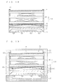
- multiple optical system units (optical unit) 50 each having the seven laminated layers 11 to 17 illustrated in FIG. 18 are made.
- the outer rim electrode parts CT1A and CT2A are formed.
- one end of the outer rim electrode part CT1A is electrically connected with the electrode pad T11a ( FIG. 4 and FIG. 5 ) formed on one surface of the image capturing element layer 11, and the other end is electrically connected with the electrode T1aA provided in the heater layer 143 in the actuator layer 14.
- one end of the outer rim electrode part CT2A is electrically connected with the electrode pad T11b ( FIG. 4 and FIG. 5 ) formed on one surface of the image capturing element layer 11, and the other end is electrically connected with the electrode T2aA provided in the heater layer 143 in the actuator layer 14.
- each layer which is a target in which outer rim electrode parts are formed is shaped and laminated and then forms the outer rim electrode parts, so that it is possible to readily make each layer to be arranged between an image capturing element layer and actuator layer in a compact imaging device formed as a laminated structure at a wafer level.
- step SP4 the cover 20 is attached to the optical unit 50.
- FIG. 19 is a view illustrating the optical unit 50 to which the cover 20 is attached.
- the optical unit 50 is installed on the assembly jig JG1. Then, the cover 20 is placed on the optical unit 50, and the fixed frame part 171 of the second parallel spring 17 and the cover 20 are bonded by, for example, an adhesive.
- the inclination of the plane to install the assembly jig JG1 is preferably within five arc-minutes (1/12 degrees).
- Step E securing of Driving Space
- step SP5 driving space of the driven body (lens layer 16) is secured.
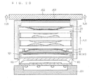
- FIG. 20 is a view for describing steps of securing the driving space of the lens layer 16.
- a cover push-up jig JG2 is installed on the upper part of the cover 20.
- the cover push-up jig JG2 has a vacuum zip part JG3 which can hold the cover 20.
- the cover push-up jig JG2 provides the push-up precision in units of sub-microns by means of a combination of an AC servo motor and piezoactuator.
- the cover 20 is pulled up in the +Z direction (direction indicated by an arrow YJ3 in FIG. 20 ) using this mechanism.
- the cover 20 is pulled up according to the amount of movement (for example, 200 ⁇ m) produced by driving the lens layer 16.
- a UV cured resin KJ1 is inserted in a gap KG between the lower part of the cover 20 which is pulled up and the optical unit 50 (see FIG. 3 ), and the UV cured resin KJ1 is cured by radiation of a ultraviolet ray.
- This UV cured resin KJ1 is cured, so that the cover 20 and image capturer PB are fixed relatively.
- the inclination of the cover 20 is limited by monitoring the changes in the distance the cover 20 is pulled up and the inclination of the cover 20.
- the cover 20 and image capturer PB are detached in the vertical direction of the lens layer 16 by pulling up the cover 20 in this way, and the first parallel spring 15 and second parallel spring 17 are each elastically deformed. Then, the lens layer 16 is made movable in the Z direction.
- step SP5 the attached cover 20 is pulled up in the +Z direction, so that the driving space of the lens layer 16 is secured.
- the actuators 14a and 14b are preferably have slight bending deformation by being pushed and bent in the -Z direction by the projecting parts 161. In other words, in a state where the cover 20 is fixed, the actuators 14a and 14b are preferably in contact with (abut on) the projecting parts 161.
- the actuators 14a and 14b of the actuator layer 14 push up the projecting parts 161 in the +Z direction when the lens layer 16 is driven by the focus adjusting operation
- a predetermined time is required until the actuators 14a and 14b contact the projecting parts 161 upon driving when, for example, the actuators 14a and 14b and projecting parts 161 are spaced apart in a still state before driving. That is, there is an idling section upon driving.
- the projecting parts 161 function to efficiently transmit driving displacement produced in the actuators 14a and 14b to the lens layer 16 which is the driven body.
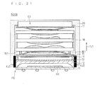
- FIG. 21 is a view illustrating a camera module 500B according to the modified example 1.
- the conductive adhesive may be provided across the lateral surfaces of the actuator layer 14, infrared cut filter layer 13 and image capturing element holder layer 12. This allows the electrodes of the image capturing element layer 11 to conduct with the heater layer through the conductive adhesive.
- a conductive adhesive and non-conductive adhesive are used in combination as adhesives where necessary to prevent short-circuiting between electrodes of the conductive adhesive corresponding to the outer rim wiring parts CT1A and CT2A.
- the camera module 500A of the above embodiment uses SMA as the displacing elements 145a and 145b, the present invention is not limited to this.
- displacing elements which function as film elements which are deformed reversibly according to a drive signal
- a thin film (piezoelectric thin film) of a piezoelectric element such as an inorganic piezoelectric body (PZT) or an organic piezoelectric body (PVDF)
- PZT inorganic piezoelectric body
- PVDF organic piezoelectric body
- an electrode, piezoelectric thin film and an electrode are formed on a Si substrate in this order using, for example, the spattering method, and is applied polling using a high electric field.
- FIG. 22 is a schematic sectional view illustrating a configuration of a camera module 500C according to a specific example 2 of the modified example.
- the camera module 500C employs the same configuration as the camera module 500A according to the above embodiment except for a penetrating wiring part CT1B (CT2B) disposed between the actuator layer 14 and image capturing element layer 11 and a penetrated hole for forming the penetrating wiring part CT1B (CT2B).
- CT1B penetrating wiring part
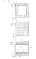
- FIG. 23 is a schematic plan view illustrating an image capturing element holder layer, an infrared cut filter layer and an actuator layer according to the specific example 2.
- FIG. 23(a) illustrates the image capturing element holder layer 12 in which penetrated holes H12T1 and H12T2 are provided in the image capturing element holder layer 12 to form the penetrating wiring part CT1B (CT2B) which transmits a drive signal to be supplied to the actuator layer 14.
- CT1B penetrating wiring part
- FIG. 23(b) illustrates the infrared cut filter layer 13 in which penetrated holes H13T1 and H13T2 are provided.
- FIG. 23(c) illustrates the actuator layer 14 having the actuators 14a and 14b which deform by being heated
- FIG. 24(b) illustrates penetrated holes H142T1 and H142T2.
- the penetrated hole H12T1 and penetrated hole H13T1 form one penetrated hole matching the penetrated hole H142T1 provided in the first insulation layer 142
- the penetrated hole H12T2 and penetrated hole H13T2 form one penetrated hole matching the penetrated hole H142T2 provided in the first insulation layer 142.
- FIG. 24 is a view for describing a detailed configuration example of an actuator layer according to the specific example 2 of the modified example.
- the penetrated hole H141T1 and penetrated hole H141T2 are provided in the base layer 141 of the actuator layer 14, and, as illustrated in FIG. 24(b) , the penetrated hole H142T1 and penetrated hole H142T2 are provided in the first insulation layer 142 of the actuator layer 14.
- FIG. 24(c) is a view illustrating a configuration of the heater layer 143 provided on the first insulation layer 142.
- Thin film resistors 143a and 143b are heated by conduction, and are formed in a predetermined shape by, for example, spattering using, for example, tantalum nitride (Ta2N) or nichrome (NiCr).
- Electrode parts T1aB, T1bB, T2aB and T2bB are made of a conductive material such as gold, and wiring parts CLaB and CLbB are also made of a conductive material such as gold and are formed using photolithography.
- the thin film resistors 143a and 143b are electrically connected in parallel to the two electrodes T1aB and T2aB. By applying the voltage between the electrodes T1aB and T2aB, the current flows to the thin film resistors 143a and 143b, and the thin film resistors 143a and 143b generate heat with Joule heat to heat the displacing elements 145a and 145b illustrated in FIG. 24(e) through the second insulation layer 144 illustrated in FIG. 24(d) .
- the penetrated hole 141T1 and penetrated hole H142T1 form one penetrated hole matching the electrode part T1aB provided in the heater layer 143
- the penetrated hole H141T2 and penetrated hole H142T2 form one penetrated hole matching the electrode part T2aB provided in the heater layer 143.
- the penetrated hole H12T1, penetrated hole H13T1, penetrated hole H141T1 and penetrated hole H142T1 form one penetrated hole matching the electrode part T1aB
- the penetrated hole H12T2, penetrated hole H13T2, penetrated hole H141T2 and penetrated hole H142T2 form one penetrated hole matching the electrode part T2aB.
- penetrated holes of several 10 micrometers are made in corner parts of the layers. Further, as a method of forming penetrated holes, a method is possible of making holes in penetrated hole parts in advance when each layer is shaped.
- a shadow mask is applied to the part except for these penetrated holes to enable electrical conduction in a vertical direction in the penetrated holes according to gold plating.
- a conductive material such as gold in the penetrated holes, the penetrating wiring parts CT1B and CT2B are formed.
- FIG. 25 is a schematic sectional view of the actuator layer 14 according to the specific example 2 of the modified example.
- the one ends of the penetrating wiring parts CT1B and CT2B are each electrically connected with the electrode parts T1aB and T2aB of the heater layer 143. Further, the other ends of the penetrating wiring parts CT1B and CT2B are electrically connected with the electrode pads T11a and T11b ( FIG. 4 and FIG. 5 ) formed on the surface on the other principal plane side of the image capturing element layer 11 (on the surface in the +Z direction).
- the camera module 500C illustrated in FIG. 22 improves the flexibility to dispose wirings by adopting the penetrating wiring system, and can readily and precisely form penetrating wiring parts (signal transmitters) disposed between the actuator layer and image capturing element layer penetrating through the image capturing element holder layer and infrared cut filter layer, in a compact image capturing element which is made as a laminated structure at a wafer level, according to a method of forming the penetrating wiring parts by making penetrated holes penetrating each layer after each layer of the wiring target is laminated or a method of making holes in advance in penetrated hole parts when each layer of the wiring target is shaped and forming penetrated wiring parts after each layer is laminated. Further, by applying an electric field to a movable part through the penetrated wiring parts (signal transmitters) formed readily and precisely, it is possible to drive the lens in a compact imaging device which is made as a laminated structure at a wafer level.
- penetrating wiring parts signal transmitters
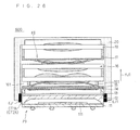
- FIG. 26 is a schematic sectional view illustrating a configuration of a camera module 600 according to a specific example 3 where the direction indicated by an arrow YJ1 is the +Z direction.
- the camera module 600 has the fixed lens layer 18 as the photo-taking optical system, the driving mechanism KB which drives the lens layer 16 as the photo-taking optical system, and the image capturer PB which acquires an image captured from the object image.
- the image capturer PB employs a configuration in which, for example, the image capturing element layer 11 having the image capturing element 111 such as a COMS sensor or a CCD sensor, the image capturing element holder layer 12 and the infrared (IR) cut filter layer 13 are laminated in this order.
- the image capturing element layer 11 having the image capturing element 111 such as a COMS sensor or a CCD sensor
- the image capturing element holder layer 12 and the infrared (IR) cut filter layer 13 are laminated in this order.
- the fixed lens layer 18 is fixed to the -Z direction surface of the cover 20 between the cover 20 and lens layer 16 and forms one photo-taking optical system in cooperation with the movable lens layer 16.
- the fixed lens layer 18 may be formed with a plurality of lens groups to contribute to improving performance of the photo-taking optical system by, for example, decreasing the aberration.
- the fixed lens layer 18 Stored in the space covered by the image capturer PB and cover 20 are the fixed lens layer 18, movable lens layer 16, first parallel spring (lower layer parallel spring) 15 and second parallel spring (upper layer parallel spring) 17 which hold the lens layer 16, and actuator layer (driving layer) 14 which functions as a driver, all of which are made in the wafer state (at a wafer level).
- the respective function layers stored in this space form the driving mechanism KB which drives the lens layer 16 in cooperation with each other.
- the cover 20, fixed lens layer 18 of the driving mechanism KB and image capturer PB serves as a fixing part for the lens layer 16.
- the lens layer 16 is supported by the first parallel spring 15 and second parallel spring 17 bonded to the fixing part. More specifically, the first parallel spring 15 is interposed between the image capturer PB and lens layer 16 on the one principal plane side (-Z side) of the lens layer 16, and the second parallel spring 17 is interposed between the fixed lens layer 18 and lens layer 16 on the other principal plane side (+Z side) of the lens layer 16.
- the first parallel spring 15 and second parallel spring 17 are each elastically deformed, and the lens layer 16 rests in a position where the elastic force of the first parallel spring 15 and the elastic force of the second parallel spring 17 balance out.
- the actuator layer 14 has an actuator which produces driving displacement in the direction (+Z direction) from the one principal plane side to the other principal plane side of the lens layer 16, and is arranged on one principal plane side of the lens layer 16 and on the other principal plane side of the image capturing element layer 11. That is, the actuator layer 14 is interposed between the image capturing element layer 11 and lens layer 16, and there is no lens element between the actuator layer 14 and image capturing element layer 11.
- the actuator contacts the projecting parts 161 projecting toward one principal plane side of the lens layer 16, and driving displacement produced in the actuator is transmitted to the lens layer 16 through the projecting parts 161.
- the outer rim wiring part CT1A (CT2A) is disposed from the image capturing element layer 11 to the actuator layer 14 along the outer rims of the image capturing element holder layer 12 and infrared (IR) cut filter layer 13, and functions as a signal transmitter which transmits a drive signal for driving the actuator.
- the camera module 600 can drive the lens of the photo-taking optical system of high performance while maintaining high reliability, in a compact imaging device which is made as a laminated structure at a wafer level by the photo-taking optical system formed with the fixed lens layer 18 and movable lens layer 16.
Landscapes
- Physics & Mathematics (AREA)
- General Physics & Mathematics (AREA)
- Optics & Photonics (AREA)
- Engineering & Computer Science (AREA)
- Multimedia (AREA)
- Signal Processing (AREA)
- Studio Devices (AREA)
- Lens Barrels (AREA)
- Camera Bodies And Camera Details Or Accessories (AREA)
- Transforming Light Signals Into Electric Signals (AREA)
Abstract
Description
- The present invention relates to a compact imaging unit and an imaging device.
- Recently, a camera module is generally installed on a compact electronic device such as a mobile telephone, and the camera module has been demanded to be made smaller.
- Conventionally, this camera module requires, for example, a lens barrel and a lens holder which support the lens, a holder which supports an infrared (IR) cut filter, a housing that holds a laminated body made up of a substrate, an image capturing element, and an optical element, a resin which seals the laminated body, and the like. Therefore, when the above multiple parts are made smaller, it has not been easy to make a camera module by precisely combining the multiple parts.
- Then, a technique is proposed in which a substrate, a semiconductor sheet formed with multiple image capturing elements and a lens array sheet formed with multiple image capturing lenses are attached with resin layers interposed therebetween to form a laminated member, and the laminated member is subjected to dicing, to complete individual camera modules (e.g., Patent Document 1, etc). Further, a technique is also proposed in which an image sensor wafer formed by arranging a plurality of image sensor chips in a matrix state, a lens array formed by integrating a plurality of lenses, an IR filter glass, and a diaphragm film are integrally attached in this order to form a structure and the structure is cut along the boundary of the image sensor chips, to complete individual camera modules (e.g., Patent Document 2, etc).
-
- Patent Document 1: Japanese Patent Application Laid-Open No.
2007-12995 - Patent Document 2: Japanese Patent Application Laid-Open No.
2004-200965 - However, although even a compact camera module has been demanded to have higher functionality of module having various functions such as an auto-focus function and a zoom function, the techniques of above Patent Documents 1 and 2 cannot sufficiently support this demand for higher functionality.
- The present invention has been made in view of the above problem, and it is an object of the present invention to provide a technique of enabling both of higher functionality and higher accuracy in a compact optical system.
- To achieve the above object, an imaging unit according to a first aspect includes a laminated structure formed by laminating a plurality of layers including: an image capturing element layer including an image capturing element part; a lens layer capable of changing a distance from the image capturing element layer; and an actuator layer including a movable part for moving the lens layer; and a signal transmitter disposed so as to connect the actuator layer and the image capturing element layer and transmitting a drive signal for driving the movable part from the image capturing element layer side to the actuator layer. In the imaging unit, the actuator layer is interposed between the image capturing element layer and the lens layer.
- An imaging unit according to a second aspect is the imaging unit according to the first aspect, wherein the laminated structure further includes another lens layer which is arranged on an opposite side of the image capturing element layer with respect to the lens layer, with a fixed distance from the image capturing element part.
- An imaging unit according to a third aspect is the imaging unit according to the first aspect, wherein the laminated structure further includes one or more function layers which are interposed between the image capturing element layer and the actuator layer, and the signal transmitter penetrates through the function layers.
- An imaging unit according to a fourth aspect is the imaging unit according to the first aspect, wherein the laminated structure further includes one or more function layers which are interposed between the image capturing element layer and the actuator layer, and the signal transmitter is disposed along outer rims of the function layers.
- An imaging unit according to a fifth aspect is the imaging unit according to the first aspect, wherein the movable part includes a film element which is reversibly deformed according to the drive signal, and moves the lens layer by means of deformation of the film element.
- An imaging unit according to a sixth aspect is the imaging unit according to the fifth aspect, wherein the movable part includes, as the film element, a thin film of a shape memory alloy attached to a substrate.
- An imaging unit according to a seventh aspect is the imaging unit according to the fifth aspect, wherein the movable part includes, as the film element, a thin film of a piezoelectric element attached to a substrate.
- An imaging device according to an eighth aspect has an imaging unit. The imaging unit includes a laminated structure formed by laminating a plurality of layers including; an image capturing element layer including an image capturing element part; a lens layer capable of changing a distance from the image capturing element layer; and an actuator layer including a movable part for moving the lens layer; and a signal transmitter disposed so as to connect the actuator layer and the image capturing element layer and transmitting a drive signal for driving the movable part from the image capturing element layer side to the actuator layer, in which the actuator layer is interposed between the image capturing element layer and the lens layer. The imaging unit receives a supply of the drive signal to drive the lens layer.
- The imaging unit according to any of the first to seventh aspects can shorten a signal transmitter which transmits the drive signal to the actuator, so that it is possible to realize a more reliable driving mechanism which achieves higher functionality in a compact imaging unit such as an imaging unit made at a wafer level.
- The imaging unit according to the second aspect can improve lens performance in the compact imaging unit while maintaining high reliability.
- With the imaging unit according to the third aspect, when imaging units including a compact driving mechanism are manufactured, by providing similar penetrating wiring parts in other sheets which are laminated and bonded to an actuator layer, it is possible to readily and precisely form a signal transmitter for applying an electrical field to a movable part.
- With the imaging unit according to the fourth aspect, it is possible to readily make each layer arranged between an image capturing element layer and an actuator layer.
-
-
FIG. 1 is a schematic view illustrating a schematic configuration of a mobile telephone on which a camera module according to an embodiment is installed. -
FIG. 2 is a schematic sectional view focusing on a first housing of the mobile telephone. -
FIG. 3 is a schematic sectional view of the camera module. -
FIG. 4 is a view illustrating an upper surface external view of an image capturing element layer to which an image capturing element is attached. -
FIG. 5 is a schematic sectional view of the image capturing element layer. -
FIG. 6 is a schematic sectional view of a lens layer. -
FIG. 7 is a lower surface external view of the lens layer. -
FIG. 8 is a view illustrating how a lens constituting layer with a third lens is made. -
FIG. 9 is an upper surface external view of a first parallel spring. -
Fig. 10 is a view illustrating the first parallel spring attached to a lens layer. -
FIG. 11 is a view illustrating an upper surface external view of an actuator layer. -
FIG. 12 is a view illustrating a lateral surface external view of the actuator layer. -
FIG. 13 is a view for describing a detailed configuration example of the actuator layer. -
FIG. 14 is a view for describing an operation example of an actuator. -
FIG. 15 is a flowchart illustrating manufacturing steps of the camera modules. -
FIG. 16 is a plan view illustrating a configuration example of sheets to be prepared. -
FIG. 17 is a view schematically illustrating how prepared sheets are laminated sequentially and bonded. -
FIG. 18 is a schematic sectional view of an optical unit. -
FIG. 19 is a view illustrating the optical unit to which a cover is attached. -
FIG. 20 is a view for describing steps of securing driving space of the lens layer. -
FIG. 21 is a view illustrating a camera module according a specific example 1 of a modified example. -
FIG. 22 is a schematic sectional view of a camera module according to a specific example 2 of the modified example. -
FIG. 23 is a schematic plan view illustrating an image capturing element holder layer, an infrared cut filter layer, and an actuator layer according to the specific example 2 of the modified example. -
FIG. 24 is a view for describing a detailed configuration example of the actuator layer according to the specific example 2 of the modified example. -
FIG. 25 is a schematic sectional view of the actuator layer according to the specific example 2 of the modified example. -
FIG. 26 is a schematic sectional view of a camera module according to a specific example 3 of the modified example. -
FIG. 1 is a schematic view illustrating a schematic configuration of amobile telephone 100 on which acamera module 500A according to an embodiment of the present invention is installed. Note that,FIG. 1 and subsequent figures are adequately assigned three X, Y and Z axes orthogonal to each other to clarify an azimuth relationship. - As illustrated in
FIG. 1 , themobile telephone 100 is formed as a folding mobile telephone, and has afirst housing 200, asecond housing 300 and ahinge part 400. - The
first housing 200 and thesecond housing 300 are each a plate rectangular parallelepiped, and function as housings which accommodate various electronic members. More specifically, thefirst housing 200 has acamera module 500A and a variable display (not illustrated), and thesecond housing 300 has a controller which electrically controls themobile telephone 100 and an operating member (not illustrated) such as buttons. - The
hinge part 400 pivotally connects thefirst housing 200 and thesecond housing 300. By this means, themobile telephone 100 is made foldable. -
FIG. 2 is a schematic sectional view focusing on thefirst housing 200 of themobile telephone 100. - As illustrated in
FIG. 1 andFIG. 2 , thecamera module 500A is a compact imaging device, that is, a micro camera unit (MCU), having a size of about 5 square mm in an X-Y cross section and a thickness (depth in the Z direction) of the order of about 3 mm. - The configuration of the
camera module 500A and its manufacturing steps will be described below in order. -
FIG. 3 is a schematic sectional view of thecamera module 500A where a direction indicated by an arrow YJ1 is a +Z direction. - As illustrated in
FIG. 3 , thecamera module 500A has a driving mechanism KB which drives alens 16 of a photo-taking optical system and an image capturer PB which acquires an image captured from an object image. - The image capturer PB has a configuration in which, for example, an image capturing
element layer 11 which has animage capturing element 111 such as a COMS sensor or a CCD sensor, an image capturingelement holder layer 12, and an infrared (IR) cutfilter layer 13 are laminated in this order. - In space covered by the image capturer PB and a
cover 20 which allows incidence of light from a ceiling surface by, for example, adopting a structure having an opening part in the ceiling surface, are stored alens layer 16, a first parallel spring (lower layer parallel spring) 15 and a second parallel spring (upper layer parallel spring) 17 which hold thelens layer 16, and a actuator layer (driving layer) 14 which functions as a driver, all of which are made in a wafer state (at a wafer level). The respective function layers stored in this space form the driving mechanism KB which drives thelens layer 16 in cooperation with each other. - More specifically, in the
camera module 500A, thecover 20 and the image capturer PB serve as a fixing part with respect to thelens layer 16. - Further, the
lens layer 16 is supported by the firstparallel spring 15 and the secondparallel spring 17 bonded to the fixing part. More specifically, the firstparallel spring 15 is interposed between the image capturer PB and thelens layer 16 on the one principal plane side (-Z side) of thelens layer 16, and the secondparallel spring 17 is interposed between thecover 20 andlens layer 16 on the other principal plane side (+Z side) of thelens layer 16. - In a non-driven state (for example, a still state before driving), the first
parallel spring 15 and the secondparallel spring 17 are each elastically deformed, and thelens layer 16 rests in a position where the elastic force of the firstparallel spring 15 and the elastic force of the secondparallel spring 17 balance out. - The
actuator layer 14 has an actuator which produces driving displacement in the direction (+Z direction) from the one principal plane side of thelens layer 16 to the other principal plane side, and is arranged on one principal plane side (the lower surface side in the illustrated example) of the lens layer 16 (more specifically, each of lens G1 to G3 ofFIG. 6 forming the lens layer 16) and on the other principal plane side (upper surface side in the illustrated example ofFIG. 3 ) of the image capturingelement layer 11. That is, theactuator layer 14 is interposed between the image capturingelement layer 11 and thelens layer 16, and there is no lens element between theactuator layer 14 and the image capturingelement layer 11. The actuatorcontacts projecting parts 161 projecting toward the one principal plane side of thelens layer 16, and driving displacement produced in the actuator is transmitted to thelens layer 16 through the projectingparts 161. An outer rim wiring part CT1A (CT2A) is disposed from the image capturingelement layer 11 to theactuator layer 14 along the outer rims of the image capturingelement holder layer 12 and the infrared (IR) cutfilter layer 13, and functions as a signal transmitter which transmits a drive signal for driving the actuator, from a predetermined electrode pad provided in the image capturingelement layer 11 which holds the image capturingelement layer 11 to theactuator layer 14. - As described above, the
camera module 500A has a laminated structure LS laminating a plurality oflayers lens layer 16 which is a driven body is bonded to elastic members arranged in positions to oppose each other across thelens layer 16 and the elastic members hold thelens layer 16 in a state of being elastically deformed toward each other in a direction vertical to the lens layer 16 (vertical direction of the lens layer 16). Then, thelens layer 16 receives the driving force from the actuator of theactuator layer 14 interposed between the image capturingelement layer 11 and thelens layer 16, and is displaced from its position. - For example, compared to a configuration of displacing the
lens layer 16 by arranging theactuator layer 14 on the opposite side of the image capturingelement layer 11 with respect to thelens layer 16, theactuator layer 14 is configured to be interposed between the image capturingelement layer 11 and thelens layer 16, so that the length of the signal transmitter becomes shorter. When the length of the signal transmitter becomes short, the number of layers in which signal transmitters are disposed can be decreased, so that it is possible to improve reliability of the driving mechanism in a compact imaging device which is made as a laminated structure at a wafer level. - Thus, the driving mechanism KB provided in the
camera module 500A can displace thelens layer 16 made at a wafer level, in the optical axis direction of thelens layer 16, and makes thecamera module 500A function as an imaging device having the lens driving function. - The details of the respective function layers forming the laminated structure LS of the
camera module 500A will be described below. Note that, with each function layer, the surface on the -Z direction side is referred to as "one principal plane side", and the surface on the +Z direction side is referred to as "the other principal plane side". -
FIG. 4 is a view illustrating an upper surface external view of the image capturingelement layer 11 to which theimage capturing element 111 is attached, and, further,FIG. 5 is a schematic sectional view of the image capturingelement layer 11 seen from a cross-sectional line 11A-11A ofFIG. 4 . - As illustrated in
FIG. 3 andFIG. 4 , the image capturingelement layer 11 is a member which has theimage capturing element 111 which generates an image signal of an object image by receiving light of the object having passed through the photo-taking optical system, its peripheral circuit C11, and an outer peripheral part F11 surrounding the peripheral circuit C11. Note that, on the surface on the one principal plane side of the image capturing element layer 11 (the lower surface side in the illustrated example ofFIG. 3 ), solder balls HB used for soldering according to a reflow scheme are provided. - As illustrated in
FIG. 4 and FIG. 5 , electrode pads T11a and T11b are formed on the surface on the other principal plane side of the image capturing element layer 11 (the upper surface side in the illustrated example ofFIG. 5 ). The electrode pads T11a and T11b are each electrically connected with outer rim electrodes CT1A and CT2A illustrated inFIG. 3 in the periphery of the image capturingelement layer 11. - On the one principal plane side of the electrode pad T11a (the lower surface side in the illustrated example of
FIG. 5 ), penetrating electrodes L11a and L11b penetrating through the image capturingelement layer 11 are formed. One end of the penetrating electrode L11a is electrically connected with the electrode pad T11a, and the other end is electrically connected with one solder ball HB provided in the surface on the one principal plane side of the image capturing element layer 11 (lower surface side in the illustrated example ofFIG. 5 ). Further, one end of the penetrating electrode L11b is electrically connected with the electrode pad T11b, and the other end is electrically connected with one of solder balls HB to which the penetrating electrode L11a is not electrically connected. - Here, when the
camera module 500A is installed on themobile telephone 100 as illustrated inFIG. 1 andFIG. 2 , the solder balls HB are electrically connected with an electronic circuit inside themobile telephone 100. The voltage (drive signals) for driving theactuator layer 14 of thecamera module 500A is generated inside themobile telephone 100, and then is supplied to theactuator layer 14 through wirings or electrodes of the penetrating electrodes L11a and L11b and outer rim electrodes CT1A and CT2A of the image capturingelement layer 11. Further, although not illustrated, various terminals for connecting wirings for giving signals to theimage capturing element 111 and reading signals from theimage capturing element 111 are provided on the surface on the other principal plane side of the image capturing element layer 11 (upper surface side in the illustrated example ofFIG. 5 ). - The image capturing
element holder layer 12 is a member which is made of, for example, a material such as resin and which holds the image capturingelement layer 11 bonded by, for example, an adhesive. An opening is provided at about the center of the image capturingelement holder layer 12. - The infrared
cut filter layer 13 is formed by layering transparent thin films of different refractive indices on a transparent substrate. - More specifically, the infrared
cut filter layer 13 is formed by, for example, spattering multiple transparent thin films of different refractive indices on the upper surface of the substrate made of a glass or transparent resin, and controls a waveband of transmitting light by means of the combination of the thickness and refractive index of the thin film. For example, the infraredcut filter layer 13, which blocks light of the waveband of 600 nm or more, is adopted. - The
lens layer 16 is made at a wafer level using a glass substrate as a base material, and is molded by, for example, overlapping two or more lenses. A case will be illustrated with the present embodiment where thelens layer 16 is formed by overlapping three lenses.FIG. 6 is a schematic sectional view of thelens layer 16 where a direction indicated by an arrow YJ2 is a +Z direction.FIG. 7 is a lower surface external view of thelens layer 16. - As illustrated in
FIG. 6 , thelens layer 16 has a lens constituting layer LY1 with a first lens G1, a lens constituting layer LY2 with a second lens G2, and a lens constituting layer LY3 with a third lens G3, and the respective lens constituting layers LY1 to LY3 are bonded in this order with ribs RB interposed therebetween. - Further, as illustrated in
FIG. 6 andFIG. 7 , projectingparts 161 in a non-lens part which does not function as a lens are provided on one principal plane of the lens constituting layer LY1 with the first lens G1. - Each of the lens constituting layers LY1 to LY3 is made according to the same method using the
glass substrate 160 as a base material.FIG. 8 is a view illustrating how the lens constituting layer LY3 with the third lens G3 is made. - More specifically, as illustrated in
FIG. 8 , an acrylic or epoxy ultraviolet (UV) cured resin of high transparency is applied to both surfaces of theglass substrate 160. Then, both surfaces are pressed by transparentlens shaping molds 162 having a shape of each lens (third lens G3 inFIG. 8 ) at a predetermined pressure and are radiated by ultraviolet rays UV1, so that polymer lenses GP1 and GP2 are each formed on the respective surfaces of theglass substrate 160. - In each of the lens constituting layers LY1 to LY3 made in this way, alignment marks for positioning are formed in two or more predetermined positions. The respective lens constituting layers LY 1 to LY3 are built up as the
integrated lens layer 16 with rib layers having the ribs RB, between each of the lens constituting layers LY1 to LY3. - More specifically, each of the lens constituting layers LY1 to LY3 and the rib layers are aligned and bonded keeping a substrate shape as is by using a mask aligner and checking respective alignment marks. A bonding method adopts a method of providing a UV cured layer in the rib layer surface to be bonded to each of the lens constituting layers LY1 to LY3 and bonding the layers by the radiation of ultraviolet rays, or a method (surface activated bonding) of radiating a plasma of inert gas on the rib layer surface and attaching and bonding the rib layer surface keeping the rib layer surface activated.
- Note that, when a diaphragm is formed in the
camera module 500A, a method of applying a shadow mask to the layer with the second lens G2 and then forming a light blocking material thin film, a method of forming a diaphragm layer using, for example, a resin material colored additionally by black, or the like is used. -
FIG. 9 is an upper surface external view of the firstparallel spring 15.FIG. 10 is a view illustrating the firstparallel spring 15 attached to thelens layer 16. - As illustrated in
FIG. 9 , the firstparallel spring 15 is an elastic member which has a fixedframe part 151 and anelastic part 152, and makes a layer (elastic layer) which forms a spring mechanism. - The fixed
frame part 151 forms an outer peripheral part of the firstparallel spring 15, and bonded to the adjacent actuator layer 14 (more specifically, the frame part F14 (described later) of the actuator layer 14). - The
elastic part 152 has a connecting part PG1 with the fixedframe part 151 and a bonding part PG2 to thelens layer 16, and the connecting part PG1 and the bonding part PG2 are connected through a plate member EB. - That is, the first
parallel spring 15 is bonded to theadjacent actuator layer 14 in the fixedframe part 151. Further, as illustrated inFIG. 10 , the firstparallel spring 15 is bonded to thelens layer 16 in the bonding part PG2 provided in theelastic part 152. By this means, when thelens layer 16 is moved in the +Z direction and the fixedframe part 151 bonded to theactuator layer 14 is detached from thelens layer 16, the positions of the connecting part PG1 and the bonding part PG2 are misaligned in the Z direction and the plate member EB is curved causing bending deformation (flexural deformation). Thus, the firstparallel spring 15 functions as a spring mechanism in a state where elastic deformation is produced in the plate member EB. - Note that, the first
parallel spring 15 is made using, for example, a SUS metal material or a phosphorus bronze. For example, when the firstparallel spring 15 is made using a SUS metal material, the shape of the parallel spring is patterned on a metal material using photolithography, is immersed in a ferric chloride etching solution and is subjected to wet etching to form the pattern of the parallel spring. - The
actuator layer 14 is a thin plate member in which a displacing element (also referred to as "actuator element") which generates the driving force is provided on the substrate such as a metal or silicon (Si).FIG. 11 is a view illustrating an upper surface external view of theactuator layer 14.FIG. 12 is a view illustrating a lateral surface external view of the actuator layer. - More specifically, as illustrated in
FIG. 11 , theactuator layer 14 has a frame part F14 forming the outer peripheral part and twoplate actuators actuators - For the displacing
elements actuators part - The SMA has characteristics that, when the SMA is heated and reaches a predetermined temperature, the SMA is restored to a predetermined shape memorized in advance (also referred to as "memorized shape"). Here, warped shapes made by free tips FT of the
actuators actuators FIG. 12 ). That is, the free tip FT sides of theactuators - Here, the detailed configuration and operation of the
actuator layer 14 will be described. -
FIG. 13 is a view for describing the detailed configuration of theactuator layer 14. - The
actuator layer 14 is formed by laminating afirst insulation layer 142 illustrated inFIG. 13(b) , aheater layer 143 illustrated inFIG. 13(c) , asecond insulation layer 144 illustrated inFIG.13(d) , and a displacingelement layer 145 illustrated inFIG. 13(e) in this order on abase layer 141 illustrated inFIG. 13(a) . Note that, theheater layer 143 illustrated inFIG. 13(c) is shown by being disposed on thefirst insulation layer 142 for ease of understanding the relationship between positions of wirings etc. - As illustrated in
FIG. 13(a) , thebase layer 141 is made of, for example, a material having adequate rigidity (for example, silicon), and is formed with a plate base member having a frame part F141 andbeam parts - The frame part F141 is a part bonded and fixed to the infrared
cut filter layer 13. Thebeam part 141a is a plate-like and arm-shaped part provided to project from one predetermined part the frame part F141, and thebeam part 141b is a plate-like and arm-shaped part provided to project from the other predetermined part of the frame part F141. Thebeam parts beam parts beam parts - that is, with this
base layer 141, each one end of thebeam parts beam parts beam parts - As illustrated in
FIG. 13(b) , thefirst insulation layer 142 is made of, for example, a non-conductive material such as a SiO2 thin film of a predetermined thickness formed by, for example, thermal oxidation, across the entire area of the upper surface of the base layer 141 (surface on the +Z side), and has the same shape as thebase layer 141. Accordingly, thefirst insulation layer 142 has a film frame part F142 formed on the upper surface of the frame part F141, andbeam parts beam parts actuator layer 14 is formed with the frame parts F141, F142 and F144 (FIG. 13(d) ) laminated mainly upward and downward. - As illustrated in
FIG. 13(c) , theheater layer 143 has twothin film resistors - The
thin film resistor 143a is provided on thebeam parts beam parts thin film resistor 143a. Further, thethin film resistor 143b has the same shape as thethin film resistor 143a, and is formed with a thin film resistor which is provided on thebeam parts beam parts thin film resistor 143b. Then, for example, tantalum nitride (Ta2N) or nichrome (NiCr) is also used for a material of thethin film resistors thin film resistors - The electrode part T1aA is a part which is made of, for example, a highly conductive metal, which is electrically connected with one end part of the
thin film resistor 143a, the outer rim wiring part CT1A illustrated inFIG. 14(b) and the wiring part CLaA, and which applies the voltage supplied through the outer rim wiring part CT1A, to thethin film resistor 143a. Further, the electrode part T2aA is a part which is made of, for example, a highly conductive metal similar to the electrode part T1aA, which is electrically connected with the other end part of thethin film resistor 143a, the outer rim wiring part CT2A illustrated inFIG. 14(b) and wiring part CLbA, and which, for example, grounds the other end part of thethin film resistor 143a through the outer rim wiring part CT2A. - The electrode part T1bA is also a part which is made of, for example, a highly conductive metal, which is electrically connected with one end part of the
thin film resistor 143b and wiring part CLaA, and which applies the voltage supplied through the outer rim wiring part CT1A, to thethin film resistor 143b. Further, the electrode part T2bA is a part which is made of, for example, a highly conductive metal similar to the electrode part T1bA, which is electrically connected with the other end part of thethin film resistor 143b and the wiring part CLbA, and which, for example, grounds the other end part of thethin film resistor 143b. - By electrically connecting the
thin film resistors thin film resistors thin film resistors - As illustrated in
FIG. 13(d) , thesecond insulation layer 144 is made of a non-conductive material, and has the same shape as thefirst insulation layer 142. Thissecond insulation layer 144 is formed across, for example, the upper surface of the first insulation layer 142 (the surface on the +Z side) and the entire area of theheater layer 143. Therefore, thesecond insulation layer 144 insulates theheater layer 143 in cooperation with thefirst insulation layer 142, and transmits heat generated by theheater layer 143 to the displacingelement layer 145 illustrated inFIG. 13(e) . Thesecond insulation layer 144 has a film frame part F144 formed on the upper surface of the frame part F142, andbeam parts beam parts - The
second insulation layer 144 is preferably a material which has insulation property and good thermal conductivity, and is formed by forming a film by, for example, spattering aluminum nitride (AIN) or alumina (AI203). - As illustrated in
FIG. 13(e) , the displacingelement layer 145 has two displacingelements - The displacing
elements elements - Note that, assume that thermal processing (memorizing thermal processing) for memorizing a shape which warps in a concave shape in the +Z direction upon heating is adequately applied to the displacing
element - Here, the operations of the
actuators actuator 14a as an example. - FIX. 14 is a view for describing the operation of the
actuator 14a.FIG. 14(a) is a plan view illustrating the configuration of theactuator layer 14 similar toFIG. 11 , andFIGS. 14(b) and 14(c) are schematic sectional views focusing on theactuator 14a seen from a cross-sectional line 6A-6A ofFIG. 14(a) . - By applying the voltage between the electrodes T1aA and T2aA through the outer rim wiring parts CT1A and CT2A disposed from the image capturing
element layer 11 to theactuator layer 14 along the outer rims of the image capturingelement holder layer 12 and infraredcut filter layer 13, the current flows to thethin film resistor 143a and thethin film resistor 143a generates heat by Joule heat. -
FIG. 14(b) illustrates a state (initial state) where theactuator 14a is not deformed. In the initial state, the voltage is not applied between the electrodes T1aA and T2aA, and thethin film resistor 143a of theheater layer 143 is at a normal temperature. Therefore, the elastic force of thebeam part 141a of thebase layer 141 makes theactuator 14a show virtually a flat shape. - When the voltage is applied between the electrodes T1aA and T2aA in the initial state illustrated in
FIG. 14(b) , the current flows to thethin film resistor 143a and thethin film resistor 143a is heated by Joule heat. The generated heat is transmitted to the displacingelement 145a through thesecond insulation layer 144a, and the displacingelement 145a is deformed to warp in a concave shape in the +Z direction when a predetermined deformation start temperature is exceeded. - Further, when application of the voltage to the electrodes T1aA and T2aA is finished, natural cooling stops deformation of the displacing
element 145a warping in a concave shape in the +Z direction and the elastic force of thebeam part 141a of thebase layer 141 restores the displacingelement 145a to the initial state which is not deformed. Thus, theactuator 14a functions as a driver which generates the driving force by being applied the electric field and deforming such that the free tips are displaced with the place contacting the frame part F14 being a fulcrum. Then, theactuator 14a abuts directly or indirectly on a moving target object, and applies an external force to the moving target object and moves this moving target object. - Note that, here, the two
thin film resistors actuator - The frame part F14 of the
actuator layer 14 is bonded to the fixedframe part 151 of the first parallel spring 15 (seeFIG. 10 ). In the bonded state, the free tip FT sides of theactuators parts 161, and displacement produced in the free tips FT of theactuators lens layer 16 through each projectingpart 161. Thus, theactuators lens layer 16. - Note that, the amount displacement produced at the free tips FT sides of the
actuators heater layer 143. - Further, although the
heater layer 143 is deformed accompanying the deformation of the SMA, the electrical resistance of theheater layer 143 changes accompanying this deformation. Therefore, the amount of displacement may be controlled by monitoring the electrical resistance value of theheater layer 143. - That is, these displacing
elements lens layer 16 by means of deformation of this film element. - As illustrated in
FIG. 9 , the secondparallel spring 17 is an elastic member which has the same configuration and function as the firstparallel spring 15, and has a fixedframe part 171 and anelastic part 172. - The fixed
frame part 171 of the secondparallel spring 17 is bonded to thecover 20, and a bonding part PG2 provided in theelastic part 172 is bonded to the other principal plane of thelens layer 16. - By this means, when the
lens layer 16 and cover 20 are detached, the plate member EB elastically deforms and the secondparallel spring 17 functions as a spring mechanism. - The
cover 20 is molded by press working using a mold by using a resin material as a material. Thecover 20 protects the driving mechanism KB and serves as a fixing part with respect to the driven body (lens layer 10). - Note that, a plurality of the
covers 20 molded in a grid pattern in a resin material are each subjected to dicing for each one of thecamera modules 500A. - Here, manufacturing steps of the
camera modules 500A will be described in detail. -
FIG. 15 is a flowchart illustrating the manufacturing steps of thecamera modules 500A. As illustrated inFIG. 15 , (step A) preparation of sheets (step SP1), (step B) bonding of sheets (step SP2), (step C) dicing (step SP3), (step D) attachment of the cover 20 (step SP4) and (step E) securing of driving space (step SP5) are performed sequentially to manufacture thecamera modules 500A. Each step will be described below. - First, in step SP1, sheets related to each function layer forming the
camera module 500A is formed per layer.FIG. 16 is a plan view illustrating a configuration of sheets to be prepared. Note that, here, the disc-shaped sheets are prepared. - In a sheet of each function layer, multiple chips corresponding to a member related to each function layer are formed in a matrix state in predetermined alignment.
- For example, as illustrated in
FIG. 16 , in the sheet (image capturing element holder sheet) HU2 of the image capturingelement holder layer 12, multiple chips corresponding to the image capturingelement holder layer 12 are formed in predetermined alignment. Note that, here, the phrase "predetermined alignment" is used to include a state where multiple chips are aligned in a predetermined direction at a predetermined interval. - The image capturing element holder sheet HU2 is made by, for example, press working using a metal mold by using a resin material as a material.
- Next, a sheet HU4 of the
actuator layer 14 will be described. - First, by adequately etching a silicon (or metal) thin plate, a base plate is formed in which multiple base layers 141 (
FIG. 13(a) ) are formed in predetermined alignment (here, predetermined alignment in a matrix state). Note that, instead of a silicon thin plate (silicon substrate), the base layers 141 may be formed with a thin plate made of polyimide and the like. - Next, the insulation film is formed on the base plate using, for example, a photolithographic method or thermal oxidation method, and the first insulation layer 142 (
FIG. 13(b) ) is formed on eachbase layer 141. Next, the heater layer 143 (FIG. 13(c) ) is formed using, for example a spattering method (or depositing method). At this time, on eachfirst insulation layer 142, thethin film resistors - Note that, the electrode parts T1aA and T2aA are preferably subjected to dicing and then formed in the positions reaching the periphery parts of individual actuator layers.
- Next, the second insulation layer 144 (
FIG. 13(d) ) is formed by forming a thin film which has insulation property and, preferably, good thermal conductivity, by using, for example, the spattering method (or depositing method). - Next, the displacing element layer 145 (
FIG. 13(e) ) is formed using, for example, the spattering method (or depositing method). At this time, the displacingelements actuators - In this way, in step SP1, similar to the image capturing element holder sheet HU2, each of the sheets HU1 and HU3 to HU7 including chips related to each function layer of the image capturing
element layer 11, infraredcut filter layer 13,actuator layer 14, firstparallel spring 15,lens layer 16, and secondparallel spring 17 is prepared. - In step SP2, each of the sheets HU1 to HU7 is bonded.
FIG. 17 is a view schematically illustrating how the prepared sheets HU1 to HU7 are sequentially laminated and bonded. - More specifically, as illustrated in
FIG. 17 , the positions of the image capturing element sheet HU1, image capturing element holder sheet HU2, infrared cut filter sheet HU3, actuator sheet HU4, first parallel spring sheet HU5, lens sheet HU6 and second parallel spring sheet HU7 are adjusted (aligned) keeping sheet shapes as is such that each chip included in each of the sheets HU1 to HU7 is laminated on each other. Then, each of the sheets HU1 to HU7 is bonded using, for example, an adhesive. - In next step SP3, a laminated member formed by laminating the seven sheets HU1 to HU7 is protected by a dicing tape and the like and then is detached per chip by the dicing apparatus. By this means, multiple optical system units (optical unit) 50 each having the seven
laminated layers 11 to 17 illustrated inFIG. 18 are made. - Next, by printing a paste of a conductive material such as silver or silver palladium in the lateral surfaces of the
actuator layer 14, the infraredcut filter layer 13 and the image capturingsensor holder layer 12, the outer rim electrode parts CT1A and CT2A are formed. At this time, one end of the outer rim electrode part CT1A is electrically connected with the electrode pad T11a (FIG. 4 and FIG. 5 ) formed on one surface of the image capturingelement layer 11, and the other end is electrically connected with the electrode T1aA provided in theheater layer 143 in theactuator layer 14. Further, one end of the outer rim electrode part CT2A is electrically connected with the electrode pad T11b (FIG. 4 and FIG. 5 ) formed on one surface of the image capturingelement layer 11, and the other end is electrically connected with the electrode T2aA provided in theheater layer 143 in theactuator layer 14. - With this outer rim electrode part forming method, each layer which is a target in which outer rim electrode parts are formed is shaped and laminated and then forms the outer rim electrode parts, so that it is possible to readily make each layer to be arranged between an image capturing element layer and actuator layer in a compact imaging device formed as a laminated structure at a wafer level.
- In step SP4, the
cover 20 is attached to theoptical unit 50.FIG. 19 is a view illustrating theoptical unit 50 to which thecover 20 is attached. - More specifically, as illustrated in
FIG. 19 , theoptical unit 50 is installed on the assembly jig JG1. Then, thecover 20 is placed on theoptical unit 50, and the fixedframe part 171 of the secondparallel spring 17 and thecover 20 are bonded by, for example, an adhesive. - Note that, the inclination of the plane to install the assembly jig JG1 is preferably within five arc-minutes (1/12 degrees).
- In step SP5, driving space of the driven body (lens layer 16) is secured.
FIG. 20 is a view for describing steps of securing the driving space of thelens layer 16. - More specifically, as illustrated in
FIG. 20 , a cover push-up jig JG2 is installed on the upper part of thecover 20. The cover push-up jig JG2 has a vacuum zip part JG3 which can hold thecover 20. Further, the cover push-up jig JG2 provides the push-up precision in units of sub-microns by means of a combination of an AC servo motor and piezoactuator. Thecover 20 is pulled up in the +Z direction (direction indicated by an arrow YJ3 inFIG. 20 ) using this mechanism. - With the present embodiment, the
cover 20 is pulled up according to the amount of movement (for example, 200 µm) produced by driving thelens layer 16. - Then, a UV cured resin KJ1 is inserted in a gap KG between the lower part of the
cover 20 which is pulled up and the optical unit 50 (seeFIG. 3 ), and the UV cured resin KJ1 is cured by radiation of a ultraviolet ray. This UV cured resin KJ1 is cured, so that thecover 20 and image capturer PB are fixed relatively. - In addition, when the
cover 20 is fixed, the inclination of thecover 20 is limited by monitoring the changes in the distance thecover 20 is pulled up and the inclination of thecover 20. - The
cover 20 and image capturer PB are detached in the vertical direction of thelens layer 16 by pulling up thecover 20 in this way, and the firstparallel spring 15 and secondparallel spring 17 are each elastically deformed. Then, thelens layer 16 is made movable in the Z direction. - Thus, in step SP5, the attached
cover 20 is pulled up in the +Z direction, so that the driving space of thelens layer 16 is secured. - Further, bending deformation (see
FIG. 19 ) of theactuators actuator layer 14 pushed and bent in the -Z direction by the projectingparts 161 is alleviated by pulling up the cover 20 (seeFIG. 20 ). - In a state where the
cover 20 is fixed by the UV cured resin KJ1 (seeFIG. 3 ), theactuators parts 161. In other words, in a state where thecover 20 is fixed, theactuators parts 161. - Although the
actuators actuator layer 14 push up the projectingparts 161 in the +Z direction when thelens layer 16 is driven by the focus adjusting operation, a predetermined time is required until theactuators parts 161 upon driving when, for example, theactuators parts 161 are spaced apart in a still state before driving. That is, there is an idling section upon driving. - However, in a state where the
cover 20 is fixed, that is, when theactuators parts 161 contact each other in advance in a still state before driving, there is no idling section, so that driving displacement produced in theactuators parts 161. - Thus, the projecting
parts 161 function to efficiently transmit driving displacement produced in theactuators lens layer 16 which is the driven body. - Although an embodiment of the present invention has been described above, the present invention is not limited to the above-described contents.
- For example, although, with the above embodiment, electrodes provided in the image capturing
element layer 11 are conducted with the heater layer through the thin outer rim wiring parts CT1A and CT2A (FIG. 3 ) provided on the lateral surfaces of theactuator layer 14, infraredcut filter layer 13 and image capturingelement holder layer 12, the present invention is not limited to this.FIG. 21 is a view illustrating acamera module 500B according to the modified example 1. - More specifically, as illustrated in
FIG. 21 , by making an adhesive KJ2 for filling the gap KG between thecover 20 and optical unit 50 a conductive adhesive, the conductive adhesive may be provided across the lateral surfaces of theactuator layer 14, infraredcut filter layer 13 and image capturingelement holder layer 12. This allows the electrodes of the image capturingelement layer 11 to conduct with the heater layer through the conductive adhesive. Further, for example, a conductive adhesive and non-conductive adhesive are used in combination as adhesives where necessary to prevent short-circuiting between electrodes of the conductive adhesive corresponding to the outer rim wiring parts CT1A and CT2A. - Further, although the
camera module 500A of the above embodiment uses SMA as the displacingelements - More specifically, as displacing elements which function as film elements which are deformed reversibly according to a drive signal, a thin film (piezoelectric thin film) of a piezoelectric element such as an inorganic piezoelectric body (PZT) or an organic piezoelectric body (PVDF) can be used. When piezoelectric films are used as displacing elements, an electrode, piezoelectric thin film and an electrode are formed on a Si substrate in this order using, for example, the spattering method, and is applied polling using a high electric field.
-
FIG. 22 is a schematic sectional view illustrating a configuration of a camera module 500C according to a specific example 2 of the modified example. - As illustrated in
FIG. 22 , the camera module 500C employs the same configuration as thecamera module 500A according to the above embodiment except for a penetrating wiring part CT1B (CT2B) disposed between theactuator layer 14 and image capturingelement layer 11 and a penetrated hole for forming the penetrating wiring part CT1B (CT2B). -
FIG. 23 is a schematic plan view illustrating an image capturing element holder layer, an infrared cut filter layer and an actuator layer according to the specific example 2. -
FIG. 23(a) illustrates the image capturingelement holder layer 12 in which penetrated holes H12T1 and H12T2 are provided in the image capturingelement holder layer 12 to form the penetrating wiring part CT1B (CT2B) which transmits a drive signal to be supplied to theactuator layer 14. -
FIG. 23(b) illustrates the infraredcut filter layer 13 in which penetrated holes H13T1 and H13T2 are provided. -
FIG. 23(c) illustrates theactuator layer 14 having theactuators FIG. 24(b) illustrates penetrated holes H142T1 and H142T2. - As illustrated in
FIG. 23(a) , when the image capturingelement holder layer 12, infraredcut filter layer 13 andactuator layer 14 are laminated, the penetrated hole H12T1 and penetrated hole H13T1 form one penetrated hole matching the penetrated hole H142T1 provided in thefirst insulation layer 142, and the penetrated hole H12T2 and penetrated hole H13T2 form one penetrated hole matching the penetrated hole H142T2 provided in thefirst insulation layer 142. -
FIG. 24 is a view for describing a detailed configuration example of an actuator layer according to the specific example 2 of the modified example. - As illustrated in
FIG. 24(a) , the penetrated hole H141T1 and penetrated hole H141T2 are provided in thebase layer 141 of theactuator layer 14, and, as illustrated inFIG. 24(b) , the penetrated hole H142T1 and penetrated hole H142T2 are provided in thefirst insulation layer 142 of theactuator layer 14. -
FIG. 24(c) is a view illustrating a configuration of theheater layer 143 provided on thefirst insulation layer 142. -
Thin film resistors - Electrode parts T1aB, T1bB, T2aB and T2bB are made of a conductive material such as gold, and wiring parts CLaB and CLbB are also made of a conductive material such as gold and are formed using photolithography.
- The
thin film resistors thin film resistors thin film resistors displacing elements FIG. 24(e) through thesecond insulation layer 144 illustrated inFIG. 24(d) . - As illustrated in
FIG. 24(a), FIG. 24(b) and FIG. 24(c) , when thebase layer 141,first insulation layer 142 andheater layer 143 of theactuator layer 14 are laminated, the penetrated hole 141T1 and penetrated hole H142T1 form one penetrated hole matching the electrode part T1aB provided in theheater layer 143, and the penetrated hole H141T2 and penetrated hole H142T2 form one penetrated hole matching the electrode part T2aB provided in theheater layer 143. - Hence, the penetrated hole H12T1, penetrated hole H13T1, penetrated hole H141T1 and penetrated hole H142T1 form one penetrated hole matching the electrode part T1aB, and the penetrated hole H12T2, penetrated hole H13T2, penetrated hole H141T2 and penetrated hole H142T2 form one penetrated hole matching the electrode part T2aB. Here, to form these penetrated holes, after target layers are laminated using femtosecond laser, excimer laser or ion etching method, penetrated holes of several 10 micrometers are made in corner parts of the layers. Further, as a method of forming penetrated holes, a method is possible of making holes in penetrated hole parts in advance when each layer is shaped.
- For example, a shadow mask is applied to the part except for these penetrated holes to enable electrical conduction in a vertical direction in the penetrated holes according to gold plating. For example, by filling a conductive material such as gold in the penetrated holes, the penetrating wiring parts CT1B and CT2B are formed.
-
FIG. 25 is a schematic sectional view of theactuator layer 14 according to the specific example 2 of the modified example. - The one ends of the penetrating wiring parts CT1B and CT2B are each electrically connected with the electrode parts T1aB and T2aB of the
heater layer 143. Further, the other ends of the penetrating wiring parts CT1B and CT2B are electrically connected with the electrode pads T11a and T11b (FIG. 4 and FIG. 5 ) formed on the surface on the other principal plane side of the image capturing element layer 11 (on the surface in the +Z direction). - As described above, the camera module 500C illustrated in
FIG. 22 improves the flexibility to dispose wirings by adopting the penetrating wiring system, and can readily and precisely form penetrating wiring parts (signal transmitters) disposed between the actuator layer and image capturing element layer penetrating through the image capturing element holder layer and infrared cut filter layer, in a compact image capturing element which is made as a laminated structure at a wafer level, according to a method of forming the penetrating wiring parts by making penetrated holes penetrating each layer after each layer of the wiring target is laminated or a method of making holes in advance in penetrated hole parts when each layer of the wiring target is shaped and forming penetrated wiring parts after each layer is laminated. Further, by applying an electric field to a movable part through the penetrated wiring parts (signal transmitters) formed readily and precisely, it is possible to drive the lens in a compact imaging device which is made as a laminated structure at a wafer level. -
FIG. 26 is a schematic sectional view illustrating a configuration of acamera module 600 according to a specific example 3 where the direction indicated by an arrow YJ1 is the +Z direction. - As illustrated in
FIG. 26 , thecamera module 600 has the fixedlens layer 18 as the photo-taking optical system, the driving mechanism KB which drives thelens layer 16 as the photo-taking optical system, and the image capturer PB which acquires an image captured from the object image. - The image capturer PB employs a configuration in which, for example, the image capturing
element layer 11 having theimage capturing element 111 such as a COMS sensor or a CCD sensor, the image capturingelement holder layer 12 and the infrared (IR) cutfilter layer 13 are laminated in this order. - The fixed
lens layer 18 is fixed to the -Z direction surface of thecover 20 between thecover 20 andlens layer 16 and forms one photo-taking optical system in cooperation with themovable lens layer 16. - With the
camera module 600, although the fixedlens layer 18 forms one lens group, the fixedlens layer 18 may be formed with a plurality of lens groups to contribute to improving performance of the photo-taking optical system by, for example, decreasing the aberration. - Stored in the space covered by the image capturer PB and cover 20 are the fixed
lens layer 18,movable lens layer 16, first parallel spring (lower layer parallel spring) 15 and second parallel spring (upper layer parallel spring) 17 which hold thelens layer 16, and actuator layer (driving layer) 14 which functions as a driver, all of which are made in the wafer state (at a wafer level). The respective function layers stored in this space form the driving mechanism KB which drives thelens layer 16 in cooperation with each other. - More specifically, with the
camera module 600, thecover 20, fixedlens layer 18 of the driving mechanism KB and image capturer PB serves as a fixing part for thelens layer 16. - Further, the
lens layer 16 is supported by the firstparallel spring 15 and secondparallel spring 17 bonded to the fixing part. More specifically, the firstparallel spring 15 is interposed between the image capturer PB andlens layer 16 on the one principal plane side (-Z side) of thelens layer 16, and the secondparallel spring 17 is interposed between the fixedlens layer 18 andlens layer 16 on the other principal plane side (+Z side) of thelens layer 16. - In a non-driven state (for example, a still state before driving), the first
parallel spring 15 and secondparallel spring 17 are each elastically deformed, and thelens layer 16 rests in a position where the elastic force of the firstparallel spring 15 and the elastic force of the secondparallel spring 17 balance out. - The
actuator layer 14 has an actuator which produces driving displacement in the direction (+Z direction) from the one principal plane side to the other principal plane side of thelens layer 16, and is arranged on one principal plane side of thelens layer 16 and on the other principal plane side of the image capturingelement layer 11. That is, theactuator layer 14 is interposed between the image capturingelement layer 11 andlens layer 16, and there is no lens element between theactuator layer 14 and image capturingelement layer 11. The actuator contacts the projectingparts 161 projecting toward one principal plane side of thelens layer 16, and driving displacement produced in the actuator is transmitted to thelens layer 16 through the projectingparts 161. The outer rim wiring part CT1A (CT2A) is disposed from the image capturingelement layer 11 to theactuator layer 14 along the outer rims of the image capturingelement holder layer 12 and infrared (IR) cutfilter layer 13, and functions as a signal transmitter which transmits a drive signal for driving the actuator. - As described above, the
camera module 600 can drive the lens of the photo-taking optical system of high performance while maintaining high reliability, in a compact imaging device which is made as a laminated structure at a wafer level by the photo-taking optical system formed with the fixedlens layer 18 andmovable lens layer 16. -
- 500A, 500B, 500C. 600 CAMERA MODULE
- 100 MOBILE TELEPHONE
- 11 IMAGE CAPTURING ELEMENT LAYER
- 111 IMAGE CAPTURING ELEMENT
- 12 IMAGE CAPTURING ELEMENT HOLDER LAYER
- 13 INFRARED CUT FILTER LAYER
- 14 ACTUATOR LAYER
- 141 BASE LAYER
- 142 FIRST INSULATION LAYER
- 143 HEATER LAYER
- 144 SECOND INSULATION LAYER
- 145 DISPLACING ELEMENT LAYER
- 14a, 14b ACTUATOR
- 141a, 141b, 142a, 142b, 144a, 144b BEAM PART
- 143a, 143b THIN FILM RESISTOR
- 145a, 145b DISPLACING ELEMENT
- 15 FIRST PARALLEL SPRING
- 16 LENS LAYER
- 161 PROJECTING PART
- 17 SECOND PARALLEL SPRING
- 18 FIXED LENS LAYER
- 20 COVER
- LS LAMINATED STRUCTURE
- T1aA, T2aA, T1bA, T2bA, T1aB, T2aB, T1bB, T2b ELECTRODE PART
- CLaA, CLbA, CLaB, CLbB WIRING PART
- CT1B, CT2B PENETRATING WIRING PART
- CT1A, CT2A OUTER RIM WIRING PART
- C11 PERIPHERAL CIRCUIT
- F11 OUTER PERIPHERAL PART
- T11a, T11b ELECTRODE PAD
- L11a, L11b PENETRATING ELECTRODE
Claims (8)
- An imaging unit comprising:a laminated structure formed by laminating a plurality of layers including:an image capturing element layer including an image capturing element part;a lens layer capable of changing a distance from said image capturing element layer; andan actuator layer including a movable part for moving said lens layer; anda signal transmitter disposed so as to connect said actuator layer and said image capturing element layer, and transmitting a drive signal for driving said movable part from said image capturing element layer side to said actuator layer,wherein said actuator layer is interposed between said image capturing element layer and said lens layer.
- The imaging unit according to claim 1, wherein
said laminated structure further includes another lens layer arranged on an opposite side of said image capturing element layer with respect to said lens layer, with a fixed distance from said image capturing element part. - The imaging unit according to claim 1, wherein
said laminated structure further includes one or more function layers interposed between said image capturing element layer and said actuator layer, and
said signal transmitter penetrates through said function layers. - The imaging unit according to claim 1, wherein
the laminated structure further includes one or more function layers interposed between said image capturing element layer and said actuator layer, and
said signal transmitter is disposed along outer rims of said function layers. - The imaging unit according to claim 1, wherein
the movable part includes a film element reversibly deformed according to said drive signal, and moves said lens layer by means of deformation of said film element. - The imaging unit according to claim 5, wherein
said movable part includes, as said film element, a thin film of a shape memory alloy attached to a substrate. - The imaging unit according to claim 5, wherein
said movable part includes, as said film element, a thin film of a piezoelectric element attached to a substrate. - An imaging device comprising an imaging unit, wherein
said imaging unit includes:a laminated structure formed by laminating a plurality of layers including:an image capturing element layer including an image capturing element part;a lens layer capable of changing a distance from said image capturing element layer; andan actuator layer including a movable part for moving said lens layer; anda signal transmitter disposed so as to connect said actuator layer and said image capturing element layer and transmitting a drive signal for driving said movable part from said image capturing element layer side to said actuator layer,said actuator layer is interposed between said image capturing element layer and said lens layer, andsaid imaging unit receives a supply of said drive signal to drive said lens layer.
Applications Claiming Priority (2)
| Application Number | Priority Date | Filing Date | Title |
|---|---|---|---|
| JP2008256556 | 2008-10-01 | ||
| PCT/JP2009/066474 WO2010038640A1 (en) | 2008-10-01 | 2009-09-24 | Imaging unit and imaging device |
Publications (2)
| Publication Number | Publication Date |
|---|---|
| EP2333599A1 true EP2333599A1 (en) | 2011-06-15 |
| EP2333599A4 EP2333599A4 (en) | 2012-03-14 |
Family
ID=42073405
Family Applications (1)
| Application Number | Title | Priority Date | Filing Date |
|---|---|---|---|
| EP09817674A Withdrawn EP2333599A4 (en) | 2008-10-01 | 2009-09-24 | IMAGING UNIT AND IMAGING DEVICE |
Country Status (4)
| Country | Link |
|---|---|
| US (1) | US8717486B2 (en) |
| EP (1) | EP2333599A4 (en) |
| JP (1) | JP5447387B2 (en) |
| WO (1) | WO2010038640A1 (en) |
Families Citing this family (28)
| Publication number | Priority date | Publication date | Assignee | Title |
|---|---|---|---|---|
| EP2333599A4 (en) | 2008-10-01 | 2012-03-14 | Konica Minolta Holdings Inc | IMAGING UNIT AND IMAGING DEVICE |
| JPWO2011055654A1 (en) * | 2009-11-05 | 2013-03-28 | コニカミノルタアドバンストレイヤー株式会社 | Imaging device and method of manufacturing the imaging device |
| US8692932B2 (en) * | 2010-11-02 | 2014-04-08 | Hong Kong Applied Science And Technology Research Institute Co., Ltd. | Compact imaging device having a laminated component |
| KR101845089B1 (en) * | 2011-11-23 | 2018-04-03 | 엘지이노텍 주식회사 | Camera module |
| JP2013229675A (en) * | 2012-04-24 | 2013-11-07 | Sony Corp | Image pickup unit and image pickup device |
| CN104798364B (en) | 2012-06-07 | 2018-08-17 | 数位光学欧洲有限公司 | MEMS Fast Focus Camera Module |
| US9001268B2 (en) | 2012-08-10 | 2015-04-07 | Nan Chang O-Film Optoelectronics Technology Ltd | Auto-focus camera module with flexible printed circuit extension |
| US9007520B2 (en) | 2012-08-10 | 2015-04-14 | Nanchang O-Film Optoelectronics Technology Ltd | Camera module with EMI shield |
| US8717487B2 (en) * | 2012-08-10 | 2014-05-06 | Digitaloptics Corporation | Camera module with compact sponge absorbing design |
| KR101446397B1 (en) * | 2012-11-30 | 2014-10-01 | 엘지이노텍 주식회사 | Camera Module |
| JP6091650B2 (en) * | 2014-04-08 | 2017-03-08 | オリンパス株式会社 | Drive device and image equipment |
| US10609262B2 (en) * | 2015-06-03 | 2020-03-31 | Lg Innotek Co., Ltd. | Lens barrel and camera module comprising same |
| TWM513520U (en) * | 2015-06-11 | 2015-12-01 | Altek Corp | Camera module |
| US10684444B2 (en) * | 2015-08-17 | 2020-06-16 | Lg Innotek Co., Ltd. | Camera module |
| JP6686349B2 (en) * | 2015-09-29 | 2020-04-22 | 大日本印刷株式会社 | Imaging module, imaging device |
| KR102528490B1 (en) * | 2015-10-30 | 2023-05-04 | 엘지이노텍 주식회사 | camara module for lens heater with temperature control |
| CN105516563A (en) * | 2015-12-15 | 2016-04-20 | 三星半导体(中国)研究开发有限公司 | Wafer level camera module |
| WO2017101853A1 (en) | 2015-12-16 | 2017-06-22 | 宁波舜宇光电信息有限公司 | Lens module and capturing module integrating focusing mechanism and assembly method therefor |
| US10230878B2 (en) * | 2016-04-08 | 2019-03-12 | Tdk Taiwan Corp. | Camera module |
| US11211772B2 (en) | 2018-06-12 | 2021-12-28 | Stmicroelectronics (Grenoble 2) Sas | Protection mechanism for light source |
| CN210153731U (en) * | 2018-06-12 | 2020-03-17 | 意法半导体(格勒诺布尔2)公司 | Housing of light source mounted on substrate and electronic device |
| US10865962B2 (en) | 2018-06-12 | 2020-12-15 | Stmicroelectronics (Grenoble 2) Sas | Protection mechanism for light source |
| FR3085465B1 (en) | 2018-08-31 | 2021-05-21 | St Microelectronics Grenoble 2 | LIGHT SOURCE PROTECTION MECHANISM |
| US11453366B2 (en) * | 2018-11-06 | 2022-09-27 | Motherson Innovations Company Limited | Heatable device for use with a vehicle-mounted image acquisition unit |
| JP7189852B2 (en) * | 2019-09-11 | 2022-12-14 | 新思考電機有限公司 | Lens driving device, camera device and electronic device |
| GB2618293A (en) * | 2021-02-22 | 2023-11-01 | Hutchinson Technology | Shape memory alloy actuators and methods thereof |
| US12075162B2 (en) | 2022-07-28 | 2024-08-27 | Dell Products L.P. | Camera with plural selective fields of view |
| US11910086B1 (en) | 2022-07-28 | 2024-02-20 | Dell Products L.P. | Small form factor active illumination privacy shutter |
Family Cites Families (23)
| Publication number | Priority date | Publication date | Assignee | Title |
|---|---|---|---|---|
| JPS607245B2 (en) * | 1980-06-10 | 1985-02-23 | ウエスト電気株式会社 | lens moving device |
| JPH0611637A (en) * | 1992-06-25 | 1994-01-21 | Toshiba Corp | Optical device |
| US7410243B2 (en) * | 1997-07-15 | 2008-08-12 | Silverbrook Research Pty Ltd | Inkjet nozzle with resiliently biased ejection actuator |
| JP2000019374A (en) * | 1998-06-29 | 2000-01-21 | Murata Mfg Co Ltd | Focusing unit and image forming device |
| US6970401B2 (en) * | 1999-06-23 | 2005-11-29 | Dphi Acquisitions, Inc. | Fringing field focus motor and mechanism for optical disk drive |
| JP2002357773A (en) | 2001-06-04 | 2002-12-13 | Olympus Optical Co Ltd | Optical component and endoscope and endoscopic optical system using the same |
| JP2004200965A (en) | 2002-12-18 | 2004-07-15 | Sanyo Electric Co Ltd | Camera module and manufacturing method thereof |
| JP2005107084A (en) * | 2003-09-30 | 2005-04-21 | Sankyo Seiki Mfg Co Ltd | Manufacturing method of lens driving device |
| FR2864526B1 (en) * | 2003-12-26 | 2006-10-13 | Commissariat Energie Atomique | ELECTROSTATIC ACTUATING DEVICE |
| JP2005352132A (en) * | 2004-06-10 | 2005-12-22 | Alps Electric Co Ltd | Camera unit |
| JP4882305B2 (en) * | 2004-08-13 | 2012-02-22 | ミツミ電機株式会社 | Autofocus actuator |
| EP1851808B1 (en) * | 2005-02-15 | 2013-08-14 | Nokia Corporation | Piezoelectric actuator element for micromovement |
| JP2006246656A (en) | 2005-03-04 | 2006-09-14 | Seiko Precision Inc | Actuator, focusing device, and image pickup unit |
| JP2007012995A (en) | 2005-07-01 | 2007-01-18 | Toshiba Corp | Ultra-small camera module and manufacturing method thereof |
| JP2007043628A (en) | 2005-08-05 | 2007-02-15 | Hitachi Maxell Ltd | The camera module |
| JP2007193248A (en) | 2006-01-23 | 2007-08-02 | Alps Electric Co Ltd | Camera module |
| DE102006013164A1 (en) * | 2006-03-22 | 2007-09-27 | Robert Bosch Gmbh | Method for mounting a camera module and camera module |
| US8175449B2 (en) | 2006-05-30 | 2012-05-08 | Konica Minolta Opto, Inc. | Driving device, driving mechanism, and image sensing apparatus |
| JP2008020812A (en) * | 2006-07-14 | 2008-01-31 | Konica Minolta Opto Inc | Lens driving mechanism and imaging apparatus using same |
| US8138564B2 (en) | 2006-07-20 | 2012-03-20 | Konica Minolta Opto, Inc. | Image sensor unit and image sensor apparatus |
| JP2008048388A (en) | 2006-07-21 | 2008-02-28 | Konica Minolta Opto Inc | Imaging unit and imaging apparatus |
| US7893965B2 (en) * | 2007-08-08 | 2011-02-22 | Bayer Materialscience Ag | Optical lens image stabilization systems |
| EP2333599A4 (en) | 2008-10-01 | 2012-03-14 | Konica Minolta Holdings Inc | IMAGING UNIT AND IMAGING DEVICE |
-
2009
- 2009-09-24 EP EP09817674A patent/EP2333599A4/en not_active Withdrawn
- 2009-09-24 US US13/121,816 patent/US8717486B2/en not_active Expired - Fee Related
- 2009-09-24 JP JP2010531814A patent/JP5447387B2/en not_active Expired - Fee Related
- 2009-09-24 WO PCT/JP2009/066474 patent/WO2010038640A1/en not_active Ceased
Also Published As
| Publication number | Publication date |
|---|---|
| EP2333599A4 (en) | 2012-03-14 |
| US20110199530A1 (en) | 2011-08-18 |
| JPWO2010038640A1 (en) | 2012-03-01 |
| WO2010038640A1 (en) | 2010-04-08 |
| US8717486B2 (en) | 2014-05-06 |
| JP5447387B2 (en) | 2014-03-19 |
Similar Documents
| Publication | Publication Date | Title |
|---|---|---|
| EP2333599A1 (en) | Imaging unit and imaging device | |
| JP5541156B2 (en) | Actuator array sheet | |
| US8715444B2 (en) | Imaging device and imaging device manufacturing method | |
| JP5056984B2 (en) | Drive device and camera module | |
| JP2010160187A (en) | Method for manufacturing drive device and method for manufacturing imaging apparatus | |
| JP2010074502A (en) | Drive unit and imaging device | |
| JP5035188B2 (en) | Imaging device manufacturing method and imaging device | |
| JP4930436B2 (en) | Lens array sheet | |
| JP2010169800A (en) | Driving device and imaging apparatus | |
| JP5115510B2 (en) | Imaging device, optical unit, and manufacturing method of imaging device | |
| JP4941389B2 (en) | Drive device | |
| JP5261749B2 (en) | Driving device and imaging device | |
| JP5422986B2 (en) | Driving device and imaging device | |
| JP5440600B2 (en) | Camera module array and manufacturing method thereof | |
| WO2010064620A1 (en) | Imaging apparatus | |
| JP5407409B2 (en) | Imaging device and manufacturing method thereof | |
| JP2010219727A (en) | Actuator, driving device and imaging device |
Legal Events
| Date | Code | Title | Description |
|---|---|---|---|
| PUAI | Public reference made under article 153(3) epc to a published international application that has entered the european phase |
Free format text: ORIGINAL CODE: 0009012 |
|
| 17P | Request for examination filed |
Effective date: 20110331 |
|
| AK | Designated contracting states |
Kind code of ref document: A1 Designated state(s): AT BE BG CH CY CZ DE DK EE ES FI FR GB GR HR HU IE IS IT LI LT LU LV MC MK MT NL NO PL PT RO SE SI SK SM TR |
|
| AX | Request for extension of the european patent |
Extension state: AL BA RS |
|
| DAX | Request for extension of the european patent (deleted) | ||
| A4 | Supplementary search report drawn up and despatched |
Effective date: 20120215 |
|
| RIC1 | Information provided on ipc code assigned before grant |
Ipc: H01L 27/146 20060101ALN20120209BHEP Ipc: G03B 3/10 20060101ALI20120209BHEP Ipc: G02B 13/00 20060101ALI20120209BHEP Ipc: G02B 7/04 20060101ALI20120209BHEP Ipc: H04N 5/225 20060101AFI20120209BHEP |
|
| STAA | Information on the status of an ep patent application or granted ep patent |
Free format text: STATUS: THE APPLICATION HAS BEEN WITHDRAWN |
|
| 18W | Application withdrawn |
Effective date: 20140910 |