EP2328059B1 - Leiterplattenmodul - Google Patents
Leiterplattenmodul Download PDFInfo
- Publication number
- EP2328059B1 EP2328059B1 EP10192320.9A EP10192320A EP2328059B1 EP 2328059 B1 EP2328059 B1 EP 2328059B1 EP 10192320 A EP10192320 A EP 10192320A EP 2328059 B1 EP2328059 B1 EP 2328059B1
- Authority
- EP
- European Patent Office
- Prior art keywords
- circuit board
- cover
- connector
- connectors
- module
- Prior art date
- Legal status (The legal status is an assumption and is not a legal conclusion. Google has not performed a legal analysis and makes no representation as to the accuracy of the status listed.)
- Active
Links
Images

Classifications
-
- G—PHYSICS
- G06—COMPUTING OR CALCULATING; COUNTING
- G06F—ELECTRIC DIGITAL DATA PROCESSING
- G06F1/00—Details not covered by groups G06F3/00 - G06F13/00 and G06F21/00
- G06F1/16—Constructional details or arrangements
- G06F1/18—Packaging or power distribution
-
- H—ELECTRICITY
- H05—ELECTRIC TECHNIQUES NOT OTHERWISE PROVIDED FOR
- H05K—PRINTED CIRCUITS; CASINGS OR CONSTRUCTIONAL DETAILS OF ELECTRIC APPARATUS; MANUFACTURE OF ASSEMBLAGES OF ELECTRICAL COMPONENTS
- H05K9/00—Screening of apparatus or components against electric or magnetic fields
- H05K9/0007—Casings
- H05K9/0018—Casings with provisions to reduce aperture leakages in walls, e.g. terminals, connectors, cables
Definitions
- the invention relates to a circuit board and, more particularly, to a circuit board with a cover.
- circuit board For better heat dissipation efficiency, some users put the circuit board out of the computer system instead of inside the system. However, it is unaesthetic to expose the circuit board outside since the circuit board has many messing components on it. Furthermore, the circuit board has many aculeate portions, and thus the users easily get hurt by an accidental touch on the aculeate portions if the aculeate portions are not covered. Moreover, if the electronic components on the circuit board contact with a human body or other conduction objects, the users may get an electric shock, or the electronic components may be damaged.
- US 2005/265003 A1 discloses a computer system, including a computer chassis configured to retain a motherboard having a plurality of I/O (input/output) connectors mounted thereon; and an electrically conductive door movable from an open position to a closed position, wherein when said door is in the open position, the I/O connectors are exposed, and when said door is in the closed position, the I/O connectors are covered.
- a method of operating a computer including a motherboard having a plurality of I/O (input/output) connectors mounted thereon is further disclosed.
- the method includes operating the computer to generate electromagnetic signals, and blocking the electromagnetic signals with an electrically conductive door movable from an open position to a closed position, wherein when said door is in the open position, the I/O connectors are exposed, and when said door is in the closed position, the I/O connectors are covered.
- a circuit board module (such as a motherboard) as defined by claim 5.
- a flow-guide structure is disposed on one side of the cover toward the circuit board of the circuit board module to guide the airflow generated by the heat dissipation units (such as a fan).
- the circuit board further may include a heat pipe contacting with the electronic components. The airflow generated by the fan passes through the heat pipe and removes the heat on the heat pipe.
- the cover further includes a shield disposed near the openings to shield the openings that are not for use temporary.
- the connectors may be a central processing unit (CPU) connector, a memory connector, a data line connector, a video graphics array (VGA) connector or a universal serial bus (USB) connector.
- CPU central processing unit
- memory a memory
- data line connector a data line connector
- VGA video graphics array
- USB universal serial bus
- the cover shields the electronic components but exposes the connectors.
- the circuit board is not only with aesthetic feelings, but also more convenient and safe for users.
- FIG.1 is an exploded diagram showing a circuit board module according to an embodiment
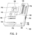
- FIG.2 is a schematic diagram showing the assembled circuit board module in FIG.1
- a circuit board module 100 in this embodiment includes a circuit board 110, a plurality of electronic components 120, a plurality of connectors 130 and a cover 140.
- the electronic components 120, the connectors 130 and the cover 140 are disposed on a first surface S10 of the circuit board 110.
- the cover 140 covers the electronic components 120.
- the cover 140 has a plurality of openings P10 exposing the connectors 130.
- the electronic components 120 may be a south bridge chipset, a north bridge chipset, a network chipset, a graphic processing unit (GPU), a sound effect chipset, a capacitor, a resistor or other electronic components.
- connectors 130 in this embodiment and is not limited thereto.
- a CPU or a memory module is selectively disposed on the circuit 110, and the number of the openings P10 may be different from that of the connectors 130.
- Some openings P10 may expose some electronic components 120 to facilitate additional heat dissipation module 150 (such as a heat dissipation unit or a fan, not shown in figures) to enhance heat dissipation efficiency of the electronic components 120.
- the connectors 130 in this embodiment includes, for example, a CPU connector, a memory connector, a data line connector (for connecting a hard disk drive (HDD), an optical disk drive (ODD) or other storage devices), a power line connector and a USB connector or other data or signals connectors with different specification.
- a CPU connector for connecting a hard disk drive (HDD), an optical disk drive (ODD) or other storage devices
- a data line connector for connecting a hard disk drive (HDD), an optical disk drive (ODD) or other storage devices
- HDD hard disk drive
- ODD optical disk drive
- USB connector or other data or signals connectors with different specification.
- the cover 140 covers the electronic components 120 but exposes the connectors 130.
- the cover 140 may cover the circuit board 110 and the electronic components 120 to provide a concise appearance.
- a tracery, a pattern or other decoration may be further formed on the cover 140 to promote the aesthetic features of the circuit board module 100.
- the cover 140 since the cover 140 only exposes the connectors 130, the positions of the connectors 130 are clear and easy to be found and it is convenient for the users to connect the circuit board module 100 with expansion cards or storage devices.
- the users would not get hurt by an accidental touch on the aculeate portions when the cover 140 covers part of the circuit board 110 and the electronic components 120.
- the cover 140 will prevent the electronic components 120 from contacting with a human body or other conductive objects, and thus to avoid the users to get an electric shock, and reduce the probability of the damages to the electronic components 120.
- the circuit board module 100 in this embodiment further includes a fan 160 disposed on an electronic component (not shown in figures) that generates heat between the circuit board 110 and the cover 140.
- the fan 160 dissipates the heat generated from the electronic components 120 in the space between the circuit board 110 and the cover 140.
- a flow-guide structure 142 is formed on one side of the cover 140 toward the circuit board 110 to guide the airflow generated by the fan 160 to increase heat dissipation efficiency.
- a heat pipe 170 is further equipped on the dissipation module 150 and disposed on the electronic components 120 on the circuit board 110 in this embodiment, and the heat pipe 170 contacts some electronic components 120 directly. In other words, the heat generated by the electronic components 120 can be removed by the heat pipe 170.
- the airflow generated by the fan 160 also gets through the heat pipe 170 to dissipate heat accumulated on the heat pipe 170. Since the flow-guide structure 142 on the cover 140 restricts and guides the airflow generated by the fan 160 appropriately, the heat dissipation efficiency is thus enhanced.
- the cover 140 in this embodiment further includes a shield 144 disposed on any one of the openings P10.
- the shield 144 is used to shield any openings as requirement, and it is freely to be detached from the openings P10 to expose the components inside the cover 140.
- the shield 144 can shield the opening P10 to prevent dust accumulating on the connector 130 and avoid the connector 130 from being damaged. It is to be understood that the shield 144 showed in this embodiment is only one, but the number of the shield 144 may be changed by demand.
- the cover shields the electronic components of the circuit board but exposes the connectors as requirement.
- the circuit board module has good appearance, is convenient and safe.
- the cover can limit and guide the airflow generated by the fan appropriately to further enhance the heat dissipation efficiency.
Landscapes
- Engineering & Computer Science (AREA)
- Theoretical Computer Science (AREA)
- Microelectronics & Electronic Packaging (AREA)
- Power Engineering (AREA)
- Human Computer Interaction (AREA)
- Physics & Mathematics (AREA)
- General Engineering & Computer Science (AREA)
- General Physics & Mathematics (AREA)
- Cooling Or The Like Of Electrical Apparatus (AREA)
Claims (10)
- Abdeckung (140) zum Abdecken eines Schaltungsmoduls (100), zusammenwirkend mit einer Leiterplatte (110), die eine Vielzahl von elektronischen Bauteilen (120) und Verbindern (130) aufweist, wobei die Abdeckung (140) umfasst:einen Körper, der einen Teil der Leiterplatte (110) bedeckt; undeine Vielzahl von Öffnungen (P10), die auf dem Körper gebildet sind, wobei die Öffnungen (P10) entsprechend zu den Verbindern (130) auf der Leiterplatte (110) gebildet sind, dadurch gekennzeichnet, dasseine Abdeckfläche der Abdeckung (140) im Wesentlichen gleich der Oberfläche der Leiterplatte (110) ist.
- Abdeckung (140) gemäß Anspruch 1, dadurch gekennzeichnet, dass an der Abdeckung (140) weiterhin eine Abschirmung (144) umfasst ist, wobei die Abschirmung (144) eine der Öffnungen (P10) abschirmt und selektiv von der Öffnung (P10) gelöst wird, um den Verbinder (130) auf der Leiterplatte (110) zur Verwendung freizulegen.
- Abdeckung (140) gemäß Anspruch 1 oder 2, dadurch gekennzeichnet, dass sie ferner umfasst:eine Strömungsführungsstruktur (142), die an einer Seite der Abdeckung (140) in Richtung der Leiterplatte (110) gebildet ist und angepasst ist, um eine Luftströmung zu der Leiterplatte zu führen.
- Abdeckung (140) gemäß einem der Ansprüche 1 bis 3, dadurch gekennzeichnet, dass die Anschlüsse (130) auf der Leiterplatte (110) einen Zentralverarbeitungseinheitsverbinder, einen Speicherverbinder, einen Datenleitungsverbinder, einen Video-Grafik-Array-Verbinder, einen Stromleitungsverbinder und einen Universell-Seriell-Busverbinder umfassen.
- Leiterplattenmodul (100), dadurch gekennzeichnet, dass es umfasst:eine Leiterplatte (110);eine Vielzahl von elektronischen Bauteilen (120), die auf der Leiterplatte (110) angeordnet sind;eine Vielzahl von Verbindern (130), die auf der Leiterplatte (110) angeordnet sind; undeine Abdeckung (140) gemäß mindestens einem der Ansprüche 1 bis 4.
- Leiterplattenmodul (100) gemäß Anspruch 5, dadurch gekennzeichnet, dass es ferner ein Wärmeableitungsmodul (150) umfasst, das mit einem der elektronischen Bauteile (120) in Kontakt steht.
- Leiterplattenmodul (100) gemäß Anspruch 6, dadurch gekennzeichnet, dass eine Strömungsführungsstruktur (142) an einer Seite der Abdeckung (140) in Richtung der Leiterplatte (110) gebildet ist, um Luftstrom innerhalb der Abdeckung (140) zu führen.
- Leiterplattenmodul (100) gemäß Anspruch 5, dadurch gekennzeichnet, dass das Wärmeableitungsmodul (150) ein Lüfter (160) ist.
- Leiterplattenmodul (100) gemäß Anspruch 5, dadurch gekennzeichnet, dass die Abdeckung (140) ferner eine abnehmbare Abschirmung (144) aufweist, die mindestens eine der Öffnungen (P10) abschirmt.
- Leiterplattenmodul (100) gemäß Anspruch 5, dadurch gekennzeichnet, dass die Verbinder (130) einen Zentralverarbeitungseinheitsverbinder, einen Speicherverbinder, einen Datenleitungsverbinder, einen Video-Grafik-Array-Verbinder, einen Stromleitungsverbinder und einen Universell-Seriell-Busverbinder umfassen.
Applications Claiming Priority (1)
| Application Number | Priority Date | Filing Date | Title |
|---|---|---|---|
| TW098140668A TWI439221B (zh) | 2009-11-27 | 2009-11-27 | 主機板 |
Publications (3)
| Publication Number | Publication Date |
|---|---|
| EP2328059A2 EP2328059A2 (de) | 2011-06-01 |
| EP2328059A3 EP2328059A3 (de) | 2011-12-21 |
| EP2328059B1 true EP2328059B1 (de) | 2018-05-02 |
Family
ID=43757215
Family Applications (1)
| Application Number | Title | Priority Date | Filing Date |
|---|---|---|---|
| EP10192320.9A Active EP2328059B1 (de) | 2009-11-27 | 2010-11-24 | Leiterplattenmodul |
Country Status (3)
| Country | Link |
|---|---|
| US (1) | US8451622B2 (de) |
| EP (1) | EP2328059B1 (de) |
| TW (1) | TWI439221B (de) |
Families Citing this family (7)
| Publication number | Priority date | Publication date | Assignee | Title |
|---|---|---|---|---|
| WO2010067451A1 (ja) * | 2008-12-12 | 2010-06-17 | Necディスプレイソリューションズ株式会社 | プロジェクタ及びプロジェクタ用のユニット |
| CN102810001B (zh) * | 2011-06-02 | 2015-02-11 | 赛恩倍吉科技顾问(深圳)有限公司 | 散热系统 |
| GB2503407B (en) * | 2011-10-10 | 2015-12-09 | Control Tech Ltd | Barrier device |
| US9448597B2 (en) * | 2013-09-17 | 2016-09-20 | Lenovo Enterprise Solutions (Singapore) Pte. Ltd. | Electronic device with serviceable CPU |
| DE102016010304A1 (de) | 2016-08-25 | 2018-03-01 | Daimler Ag | Leiterplatte mit zumindest einem elektrischen Bauelement und einer ersten Kühlvorrichtung |
| US10108234B1 (en) * | 2017-06-09 | 2018-10-23 | Nzxt Inc. | Shielded motherboard |
| TWI777489B (zh) * | 2021-04-12 | 2022-09-11 | 巧連科技股份有限公司 | 具雙type c公頭連接裝置 |
Family Cites Families (14)
| Publication number | Priority date | Publication date | Assignee | Title |
|---|---|---|---|---|
| JP3231349B2 (ja) * | 1991-05-07 | 2001-11-19 | 富士電機株式会社 | コンピュータシステム |
| US5566050A (en) * | 1992-07-17 | 1996-10-15 | Kabushiki Kaisha Toshiba | Compact electronic apparatus having a detachable optional component |
| US5414597A (en) * | 1994-05-04 | 1995-05-09 | Ford Motor Company | Shielded circuit module |
| US6088224A (en) * | 1997-12-03 | 2000-07-11 | Emc Corporation | Cabinet for storing a plurality of processing unit modules |
| US6324075B1 (en) * | 1999-12-20 | 2001-11-27 | Intel Corporation | Partially covered motherboard with EMI partition gateway |
| US7035102B2 (en) * | 2004-01-08 | 2006-04-25 | Apple Computer, Inc. | Apparatus for air cooling of an electronic device |
| US7411784B2 (en) * | 2004-05-07 | 2008-08-12 | Rackable Systems, Inc. | Electromagnetic interference shield for I/O ports |
| US7397670B2 (en) * | 2004-07-13 | 2008-07-08 | Zippy Technology Corp. | Power supply device, power supply module and retrieval power supply device equipped with AC and DC connection structures |
| CN2849809Y (zh) * | 2005-11-11 | 2006-12-20 | 鸿富锦精密工业(深圳)有限公司 | 计算机模组机架 |
| CN101004625A (zh) | 2006-01-20 | 2007-07-25 | 佛山市顺德区顺达电脑厂有限公司 | 具有防电磁干扰屏蔽罩的主机装置 |
| DE102006006565A1 (de) * | 2006-02-13 | 2007-08-16 | E.E.P.D. Electronic Equipment Produktion & Distribution Gmbh | Abschirmung im Bereich einer elektrischen Verbindungseinrichtung, die an einer Aussparung einer Gehäusewand montiert ist |
| CN200969449Y (zh) * | 2006-09-28 | 2007-10-31 | 鸿富锦精密工业(深圳)有限公司 | 输入/输出接口遮蔽装置 |
| CN101312635B (zh) | 2007-05-21 | 2010-07-28 | 凌华科技股份有限公司 | 具有热管与散热片的导风罩及装设所述导风罩的电子装置 |
| US8081422B2 (en) * | 2008-10-02 | 2011-12-20 | Fujitsu Limited | Power distribution system |
-
2009
- 2009-11-27 TW TW098140668A patent/TWI439221B/zh active
-
2010
- 2010-11-24 EP EP10192320.9A patent/EP2328059B1/de active Active
- 2010-11-26 US US12/954,678 patent/US8451622B2/en active Active
Non-Patent Citations (1)
| Title |
|---|
| None * |
Also Published As
| Publication number | Publication date |
|---|---|
| TW201119564A (en) | 2011-06-01 |
| US20110128702A1 (en) | 2011-06-02 |
| US8451622B2 (en) | 2013-05-28 |
| TWI439221B (zh) | 2014-05-21 |
| EP2328059A2 (de) | 2011-06-01 |
| EP2328059A3 (de) | 2011-12-21 |
Similar Documents
| Publication | Publication Date | Title |
|---|---|---|
| US8451622B2 (en) | Circuit board module | |
| US20120287570A1 (en) | Computer enclosure and data storage device bracket of the computer enclosure | |
| US7298615B2 (en) | Computing device | |
| US8164900B2 (en) | Enclosure of electronic device | |
| CN102027646B (zh) | 通用串行总线连接器、存储器驱动器及承载系统 | |
| US20080200041A1 (en) | Storage device | |
| CN104168749B (zh) | 电子装置及电磁干扰屏蔽结构 | |
| US10531598B2 (en) | Fans in series with cable plug interfaces | |
| JP2002229679A (ja) | Pcカード用スロット付電子機器及びpci拡張アダプタ | |
| US20080186666A1 (en) | Motherboard and desktop host using the same | |
| EP2795730A1 (de) | Steckverbinder mit hoher bandbreite für interne und externe e/a-schnittstellen | |
| TWI452570B (zh) | 硬碟背板結構及採用該硬碟背板結構之硬碟散熱組件 | |
| TW201109897A (en) | I/O cover plate and its motherboard module | |
| US9125324B2 (en) | Motherboard | |
| JP4520354B2 (ja) | 情報処理装置 | |
| CN200969449Y (zh) | 输入/输出接口遮蔽装置 | |
| CN101853745A (zh) | 电源开关模块及具有该电源开关模块的电子装置 | |
| JP2006202256A (ja) | コンピュータ用インターフェイスカード | |
| US20060184704A1 (en) | Balanced technology extended (BTX) motherboard assembly | |
| US20100020478A1 (en) | Electronic apparatus and motherboard thereof | |
| US8605439B2 (en) | Electronic device with mechanism for securing connector thereof | |
| US20080239664A1 (en) | Heat dissipating system for computer | |
| TWI711830B (zh) | 電腦系統 | |
| CN220438831U (zh) | 机壳与主机 | |
| CN2526889Y (zh) | 具有护套的扩充槽结构 |
Legal Events
| Date | Code | Title | Description |
|---|---|---|---|
| PUAI | Public reference made under article 153(3) epc to a published international application that has entered the european phase |
Free format text: ORIGINAL CODE: 0009012 |
|
| AK | Designated contracting states |
Kind code of ref document: A2 Designated state(s): AL AT BE BG CH CY CZ DE DK EE ES FI FR GB GR HR HU IE IS IT LI LT LU LV MC MK MT NL NO PL PT RO RS SE SI SK SM TR |
|
| AX | Request for extension of the european patent |
Extension state: BA ME |
|
| PUAL | Search report despatched |
Free format text: ORIGINAL CODE: 0009013 |
|
| AK | Designated contracting states |
Kind code of ref document: A3 Designated state(s): AL AT BE BG CH CY CZ DE DK EE ES FI FR GB GR HR HU IE IS IT LI LT LU LV MC MK MT NL NO PL PT RO RS SE SI SK SM TR |
|
| AX | Request for extension of the european patent |
Extension state: BA ME |
|
| RIC1 | Information provided on ipc code assigned before grant |
Ipc: G06F 1/18 20060101AFI20111116BHEP Ipc: H05K 9/00 20060101ALI20111116BHEP |
|
| 17P | Request for examination filed |
Effective date: 20120329 |
|
| GRAP | Despatch of communication of intention to grant a patent |
Free format text: ORIGINAL CODE: EPIDOSNIGR1 |
|
| STAA | Information on the status of an ep patent application or granted ep patent |
Free format text: STATUS: GRANT OF PATENT IS INTENDED |
|
| INTG | Intention to grant announced |
Effective date: 20171213 |
|
| GRAS | Grant fee paid |
Free format text: ORIGINAL CODE: EPIDOSNIGR3 |
|
| GRAA | (expected) grant |
Free format text: ORIGINAL CODE: 0009210 |
|
| STAA | Information on the status of an ep patent application or granted ep patent |
Free format text: STATUS: THE PATENT HAS BEEN GRANTED |
|
| RAP1 | Party data changed (applicant data changed or rights of an application transferred) |
Owner name: ASUSTEK COMPUTER INC. |
|
| RIN1 | Information on inventor provided before grant (corrected) |
Inventor name: YU, YEN-PO |
|
| AK | Designated contracting states |
Kind code of ref document: B1 Designated state(s): AL AT BE BG CH CY CZ DE DK EE ES FI FR GB GR HR HU IE IS IT LI LT LU LV MC MK MT NL NO PL PT RO RS SE SI SK SM TR |
|
| REG | Reference to a national code |
Ref country code: GB Ref legal event code: FG4D |
|
| REG | Reference to a national code |
Ref country code: CH Ref legal event code: EP Ref country code: AT Ref legal event code: REF Ref document number: 995920 Country of ref document: AT Kind code of ref document: T Effective date: 20180515 |
|
| REG | Reference to a national code |
Ref country code: DE Ref legal event code: R096 Ref document number: 602010050327 Country of ref document: DE |
|
| REG | Reference to a national code |
Ref country code: IE Ref legal event code: FG4D |
|
| REG | Reference to a national code |
Ref country code: NL Ref legal event code: MP Effective date: 20180502 |
|
| REG | Reference to a national code |
Ref country code: FR Ref legal event code: PLFP Year of fee payment: 9 |
|
| REG | Reference to a national code |
Ref country code: LT Ref legal event code: MG4D |
|
| PG25 | Lapsed in a contracting state [announced via postgrant information from national office to epo] |
Ref country code: NO Free format text: LAPSE BECAUSE OF FAILURE TO SUBMIT A TRANSLATION OF THE DESCRIPTION OR TO PAY THE FEE WITHIN THE PRESCRIBED TIME-LIMIT Effective date: 20180802 Ref country code: BG Free format text: LAPSE BECAUSE OF FAILURE TO SUBMIT A TRANSLATION OF THE DESCRIPTION OR TO PAY THE FEE WITHIN THE PRESCRIBED TIME-LIMIT Effective date: 20180802 Ref country code: SE Free format text: LAPSE BECAUSE OF FAILURE TO SUBMIT A TRANSLATION OF THE DESCRIPTION OR TO PAY THE FEE WITHIN THE PRESCRIBED TIME-LIMIT Effective date: 20180502 Ref country code: FI Free format text: LAPSE BECAUSE OF FAILURE TO SUBMIT A TRANSLATION OF THE DESCRIPTION OR TO PAY THE FEE WITHIN THE PRESCRIBED TIME-LIMIT Effective date: 20180502 Ref country code: ES Free format text: LAPSE BECAUSE OF FAILURE TO SUBMIT A TRANSLATION OF THE DESCRIPTION OR TO PAY THE FEE WITHIN THE PRESCRIBED TIME-LIMIT Effective date: 20180502 Ref country code: LT Free format text: LAPSE BECAUSE OF FAILURE TO SUBMIT A TRANSLATION OF THE DESCRIPTION OR TO PAY THE FEE WITHIN THE PRESCRIBED TIME-LIMIT Effective date: 20180502 |
|
| PG25 | Lapsed in a contracting state [announced via postgrant information from national office to epo] |
Ref country code: LV Free format text: LAPSE BECAUSE OF FAILURE TO SUBMIT A TRANSLATION OF THE DESCRIPTION OR TO PAY THE FEE WITHIN THE PRESCRIBED TIME-LIMIT Effective date: 20180502 Ref country code: HR Free format text: LAPSE BECAUSE OF FAILURE TO SUBMIT A TRANSLATION OF THE DESCRIPTION OR TO PAY THE FEE WITHIN THE PRESCRIBED TIME-LIMIT Effective date: 20180502 Ref country code: NL Free format text: LAPSE BECAUSE OF FAILURE TO SUBMIT A TRANSLATION OF THE DESCRIPTION OR TO PAY THE FEE WITHIN THE PRESCRIBED TIME-LIMIT Effective date: 20180502 Ref country code: GR Free format text: LAPSE BECAUSE OF FAILURE TO SUBMIT A TRANSLATION OF THE DESCRIPTION OR TO PAY THE FEE WITHIN THE PRESCRIBED TIME-LIMIT Effective date: 20180803 Ref country code: RS Free format text: LAPSE BECAUSE OF FAILURE TO SUBMIT A TRANSLATION OF THE DESCRIPTION OR TO PAY THE FEE WITHIN THE PRESCRIBED TIME-LIMIT Effective date: 20180502 |
|
| REG | Reference to a national code |
Ref country code: AT Ref legal event code: MK05 Ref document number: 995920 Country of ref document: AT Kind code of ref document: T Effective date: 20180502 |
|
| PG25 | Lapsed in a contracting state [announced via postgrant information from national office to epo] |
Ref country code: PT Free format text: LAPSE BECAUSE OF FAILURE TO SUBMIT A TRANSLATION OF THE DESCRIPTION OR TO PAY THE FEE WITHIN THE PRESCRIBED TIME-LIMIT Effective date: 20180903 |
|
| PG25 | Lapsed in a contracting state [announced via postgrant information from national office to epo] |
Ref country code: DK Free format text: LAPSE BECAUSE OF FAILURE TO SUBMIT A TRANSLATION OF THE DESCRIPTION OR TO PAY THE FEE WITHIN THE PRESCRIBED TIME-LIMIT Effective date: 20180502 Ref country code: PL Free format text: LAPSE BECAUSE OF FAILURE TO SUBMIT A TRANSLATION OF THE DESCRIPTION OR TO PAY THE FEE WITHIN THE PRESCRIBED TIME-LIMIT Effective date: 20180502 Ref country code: EE Free format text: LAPSE BECAUSE OF FAILURE TO SUBMIT A TRANSLATION OF THE DESCRIPTION OR TO PAY THE FEE WITHIN THE PRESCRIBED TIME-LIMIT Effective date: 20180502 Ref country code: AT Free format text: LAPSE BECAUSE OF FAILURE TO SUBMIT A TRANSLATION OF THE DESCRIPTION OR TO PAY THE FEE WITHIN THE PRESCRIBED TIME-LIMIT Effective date: 20180502 Ref country code: CZ Free format text: LAPSE BECAUSE OF FAILURE TO SUBMIT A TRANSLATION OF THE DESCRIPTION OR TO PAY THE FEE WITHIN THE PRESCRIBED TIME-LIMIT Effective date: 20180502 Ref country code: RO Free format text: LAPSE BECAUSE OF FAILURE TO SUBMIT A TRANSLATION OF THE DESCRIPTION OR TO PAY THE FEE WITHIN THE PRESCRIBED TIME-LIMIT Effective date: 20180502 Ref country code: SK Free format text: LAPSE BECAUSE OF FAILURE TO SUBMIT A TRANSLATION OF THE DESCRIPTION OR TO PAY THE FEE WITHIN THE PRESCRIBED TIME-LIMIT Effective date: 20180502 |
|
| REG | Reference to a national code |
Ref country code: DE Ref legal event code: R097 Ref document number: 602010050327 Country of ref document: DE |
|
| PG25 | Lapsed in a contracting state [announced via postgrant information from national office to epo] |
Ref country code: SM Free format text: LAPSE BECAUSE OF FAILURE TO SUBMIT A TRANSLATION OF THE DESCRIPTION OR TO PAY THE FEE WITHIN THE PRESCRIBED TIME-LIMIT Effective date: 20180502 Ref country code: IT Free format text: LAPSE BECAUSE OF FAILURE TO SUBMIT A TRANSLATION OF THE DESCRIPTION OR TO PAY THE FEE WITHIN THE PRESCRIBED TIME-LIMIT Effective date: 20180502 |
|
| PLBE | No opposition filed within time limit |
Free format text: ORIGINAL CODE: 0009261 |
|
| STAA | Information on the status of an ep patent application or granted ep patent |
Free format text: STATUS: NO OPPOSITION FILED WITHIN TIME LIMIT |
|
| 26N | No opposition filed |
Effective date: 20190205 |
|
| PG25 | Lapsed in a contracting state [announced via postgrant information from national office to epo] |
Ref country code: SI Free format text: LAPSE BECAUSE OF FAILURE TO SUBMIT A TRANSLATION OF THE DESCRIPTION OR TO PAY THE FEE WITHIN THE PRESCRIBED TIME-LIMIT Effective date: 20180502 |
|
| REG | Reference to a national code |
Ref country code: CH Ref legal event code: PL |
|
| PG25 | Lapsed in a contracting state [announced via postgrant information from national office to epo] |
Ref country code: LU Free format text: LAPSE BECAUSE OF NON-PAYMENT OF DUE FEES Effective date: 20181124 Ref country code: MC Free format text: LAPSE BECAUSE OF FAILURE TO SUBMIT A TRANSLATION OF THE DESCRIPTION OR TO PAY THE FEE WITHIN THE PRESCRIBED TIME-LIMIT Effective date: 20180502 |
|
| REG | Reference to a national code |
Ref country code: BE Ref legal event code: MM Effective date: 20181130 |
|
| REG | Reference to a national code |
Ref country code: IE Ref legal event code: MM4A |
|
| PG25 | Lapsed in a contracting state [announced via postgrant information from national office to epo] |
Ref country code: LI Free format text: LAPSE BECAUSE OF NON-PAYMENT OF DUE FEES Effective date: 20181130 Ref country code: CH Free format text: LAPSE BECAUSE OF NON-PAYMENT OF DUE FEES Effective date: 20181130 |
|
| PG25 | Lapsed in a contracting state [announced via postgrant information from national office to epo] |
Ref country code: IE Free format text: LAPSE BECAUSE OF NON-PAYMENT OF DUE FEES Effective date: 20181124 |
|
| PG25 | Lapsed in a contracting state [announced via postgrant information from national office to epo] |
Ref country code: BE Free format text: LAPSE BECAUSE OF NON-PAYMENT OF DUE FEES Effective date: 20181130 Ref country code: AL Free format text: LAPSE BECAUSE OF FAILURE TO SUBMIT A TRANSLATION OF THE DESCRIPTION OR TO PAY THE FEE WITHIN THE PRESCRIBED TIME-LIMIT Effective date: 20180502 |
|
| PG25 | Lapsed in a contracting state [announced via postgrant information from national office to epo] |
Ref country code: MT Free format text: LAPSE BECAUSE OF NON-PAYMENT OF DUE FEES Effective date: 20181124 |
|
| PG25 | Lapsed in a contracting state [announced via postgrant information from national office to epo] |
Ref country code: TR Free format text: LAPSE BECAUSE OF FAILURE TO SUBMIT A TRANSLATION OF THE DESCRIPTION OR TO PAY THE FEE WITHIN THE PRESCRIBED TIME-LIMIT Effective date: 20180502 |
|
| PG25 | Lapsed in a contracting state [announced via postgrant information from national office to epo] |
Ref country code: CY Free format text: LAPSE BECAUSE OF FAILURE TO SUBMIT A TRANSLATION OF THE DESCRIPTION OR TO PAY THE FEE WITHIN THE PRESCRIBED TIME-LIMIT Effective date: 20180502 Ref country code: MK Free format text: LAPSE BECAUSE OF NON-PAYMENT OF DUE FEES Effective date: 20180502 Ref country code: HU Free format text: LAPSE BECAUSE OF FAILURE TO SUBMIT A TRANSLATION OF THE DESCRIPTION OR TO PAY THE FEE WITHIN THE PRESCRIBED TIME-LIMIT; INVALID AB INITIO Effective date: 20101124 |
|
| PG25 | Lapsed in a contracting state [announced via postgrant information from national office to epo] |
Ref country code: IS Free format text: LAPSE BECAUSE OF FAILURE TO SUBMIT A TRANSLATION OF THE DESCRIPTION OR TO PAY THE FEE WITHIN THE PRESCRIBED TIME-LIMIT Effective date: 20180902 |
|
| P01 | Opt-out of the competence of the unified patent court (upc) registered |
Effective date: 20230427 |
|
| PGFP | Annual fee paid to national office [announced via postgrant information from national office to epo] |
Ref country code: GB Payment date: 20250901 Year of fee payment: 16 |
|
| PGFP | Annual fee paid to national office [announced via postgrant information from national office to epo] |
Ref country code: FR Payment date: 20250901 Year of fee payment: 16 |
|
| PGFP | Annual fee paid to national office [announced via postgrant information from national office to epo] |
Ref country code: DE Payment date: 20250821 Year of fee payment: 16 |