EP2323409A2 - Image sensor with charge binning - Google Patents
Image sensor with charge binning Download PDFInfo
- Publication number
- EP2323409A2 EP2323409A2 EP11156524.8A EP11156524A EP2323409A2 EP 2323409 A2 EP2323409 A2 EP 2323409A2 EP 11156524 A EP11156524 A EP 11156524A EP 2323409 A2 EP2323409 A2 EP 2323409A2
- Authority
- EP
- European Patent Office
- Prior art keywords
- signal
- row
- pixel
- image sensor
- item
- Prior art date
- Legal status (The legal status is an assumption and is not a legal conclusion. Google has not performed a legal analysis and makes no representation as to the accuracy of the status listed.)
- Granted
Links
- 230000007246 mechanism Effects 0.000 claims abstract description 12
- 230000010354 integration Effects 0.000 claims abstract description 10
- 238000012935 Averaging Methods 0.000 claims description 9
- 238000000034 method Methods 0.000 claims description 9
- 238000010586 diagram Methods 0.000 description 24
- 238000009792 diffusion process Methods 0.000 description 17
- AAOVKJBEBIDNHE-UHFFFAOYSA-N diazepam Chemical compound N=1CC(=O)N(C)C2=CC=C(Cl)C=C2C=1C1=CC=CC=C1 AAOVKJBEBIDNHE-UHFFFAOYSA-N 0.000 description 14
- 238000006243 chemical reaction Methods 0.000 description 13
- 230000035945 sensitivity Effects 0.000 description 10
- 230000008901 benefit Effects 0.000 description 8
- 238000012545 processing Methods 0.000 description 7
- 230000009977 dual effect Effects 0.000 description 6
- 238000013459 approach Methods 0.000 description 5
- 238000012546 transfer Methods 0.000 description 5
- 238000000926 separation method Methods 0.000 description 4
- 239000003086 colorant Substances 0.000 description 3
- 238000003384 imaging method Methods 0.000 description 3
- 230000008569 process Effects 0.000 description 3
- 230000009467 reduction Effects 0.000 description 3
- 238000005070 sampling Methods 0.000 description 3
- 230000008859 change Effects 0.000 description 2
- 230000007423 decrease Effects 0.000 description 2
- 238000013461 design Methods 0.000 description 2
- 238000005286 illumination Methods 0.000 description 2
- 238000005096 rolling process Methods 0.000 description 2
- 229920000954 Polyglycolide Polymers 0.000 description 1
- 239000003990 capacitor Substances 0.000 description 1
- 238000012937 correction Methods 0.000 description 1
- 230000002596 correlated effect Effects 0.000 description 1
- 230000000694 effects Effects 0.000 description 1
- 238000002955 isolation Methods 0.000 description 1
- 238000012986 modification Methods 0.000 description 1
- 230000004048 modification Effects 0.000 description 1
- 235000010409 propane-1,2-diol alginate Nutrition 0.000 description 1
- 238000012552 review Methods 0.000 description 1
- 239000004065 semiconductor Substances 0.000 description 1
- 239000007787 solid Substances 0.000 description 1
- 230000002123 temporal effect Effects 0.000 description 1
Images


Classifications
-
- H—ELECTRICITY
- H04—ELECTRIC COMMUNICATION TECHNIQUE
- H04N—PICTORIAL COMMUNICATION, e.g. TELEVISION
- H04N25/00—Circuitry of solid-state image sensors [SSIS]; Control thereof
- H04N25/70—SSIS architectures; Circuits associated therewith
- H04N25/76—Addressed sensors, e.g. MOS or CMOS sensors
- H04N25/77—Pixel circuitry, e.g. memories, A/D converters, pixel amplifiers, shared circuits or shared components
-
- H—ELECTRICITY
- H04—ELECTRIC COMMUNICATION TECHNIQUE
- H04N—PICTORIAL COMMUNICATION, e.g. TELEVISION
- H04N25/00—Circuitry of solid-state image sensors [SSIS]; Control thereof
- H04N25/40—Extracting pixel data from image sensors by controlling scanning circuits, e.g. by modifying the number of pixels sampled or to be sampled
- H04N25/46—Extracting pixel data from image sensors by controlling scanning circuits, e.g. by modifying the number of pixels sampled or to be sampled by combining or binning pixels
-
- H—ELECTRICITY
- H04—ELECTRIC COMMUNICATION TECHNIQUE
- H04N—PICTORIAL COMMUNICATION, e.g. TELEVISION
- H04N25/00—Circuitry of solid-state image sensors [SSIS]; Control thereof
- H04N25/10—Circuitry of solid-state image sensors [SSIS]; Control thereof for transforming different wavelengths into image signals
- H04N25/11—Arrangement of colour filter arrays [CFA]; Filter mosaics
- H04N25/13—Arrangement of colour filter arrays [CFA]; Filter mosaics characterised by the spectral characteristics of the filter elements
- H04N25/134—Arrangement of colour filter arrays [CFA]; Filter mosaics characterised by the spectral characteristics of the filter elements based on three different wavelength filter elements
-
- H—ELECTRICITY
- H04—ELECTRIC COMMUNICATION TECHNIQUE
- H04N—PICTORIAL COMMUNICATION, e.g. TELEVISION
- H04N25/00—Circuitry of solid-state image sensors [SSIS]; Control thereof
- H04N25/70—SSIS architectures; Circuits associated therewith
-
- H—ELECTRICITY
- H04—ELECTRIC COMMUNICATION TECHNIQUE
- H04N—PICTORIAL COMMUNICATION, e.g. TELEVISION
- H04N25/00—Circuitry of solid-state image sensors [SSIS]; Control thereof
- H04N25/70—SSIS architectures; Circuits associated therewith
- H04N25/71—Charge-coupled device [CCD] sensors; Charge-transfer registers specially adapted for CCD sensors
- H04N25/75—Circuitry for providing, modifying or processing image signals from the pixel array
-
- H—ELECTRICITY
- H04—ELECTRIC COMMUNICATION TECHNIQUE
- H04N—PICTORIAL COMMUNICATION, e.g. TELEVISION
- H04N25/00—Circuitry of solid-state image sensors [SSIS]; Control thereof
- H04N25/70—SSIS architectures; Circuits associated therewith
- H04N25/76—Addressed sensors, e.g. MOS or CMOS sensors
- H04N25/767—Horizontal readout lines, multiplexers or registers
-
- H—ELECTRICITY
- H04—ELECTRIC COMMUNICATION TECHNIQUE
- H04N—PICTORIAL COMMUNICATION, e.g. TELEVISION
- H04N3/00—Scanning details of television systems; Combination thereof with generation of supply voltages
- H04N3/10—Scanning details of television systems; Combination thereof with generation of supply voltages by means not exclusively optical-mechanical
- H04N3/14—Scanning details of television systems; Combination thereof with generation of supply voltages by means not exclusively optical-mechanical by means of electrically scanned solid-state devices
- H04N3/15—Scanning details of television systems; Combination thereof with generation of supply voltages by means not exclusively optical-mechanical by means of electrically scanned solid-state devices for picture signal generation
- H04N3/155—Control of the image-sensor operation, e.g. image processing within the image-sensor
- H04N3/1562—Control of the image-sensor operation, e.g. image processing within the image-sensor for selective scanning, e.g. windowing, zooming
-
- H—ELECTRICITY
- H04—ELECTRIC COMMUNICATION TECHNIQUE
- H04N—PICTORIAL COMMUNICATION, e.g. TELEVISION
- H04N23/00—Cameras or camera modules comprising electronic image sensors; Control thereof
- H04N23/80—Camera processing pipelines; Components thereof
- H04N23/84—Camera processing pipelines; Components thereof for processing colour signals
Definitions
- the present invention pertains to semiconductor based image sensors such as Active Pixel image sensors (APS), and Passive Pixel image sensors (PPS), and more particularly, to such APS and PPS with charge binning, high sensitivity, low noise, and parallel channel readout.
- APS Active Pixel image sensors
- PPS Passive Pixel image sensors
- APS and PPS are x-y addressable solid state imagers wherein each pixel contains both a photosensing element and a select element.
- each pixel also contains at least one other active circuit component.
- incident illumination is converted to a signal (either a voltage or current signal).
- the signal represents the amount of light incident upon a pixel photosite.
- This signal is typically readout one row at time, and the signals for a given row are stored temporarily in a circuit associated with each column of the image sensor. This column circuit is typically constructed to fit into the size or pitch of the pixel.
- the video rate desired is 30 frames per second.
- Prior art APS and PPS sensors have accomplished video rate data from large resolution sensors by windowing or sub-sampling of the image array using the x-y addressability feature of APS and PPS sensors. While this approach provides video rate data, it does so by selective readout of the small pixels and still has poor image quality in low light level environments, and produces aliasing image artifacts.
- Some APS and PPS sensors also include on sensor white balance by placing a programmable gain amplifier PGA in the readout path, which gain can change at a pixel data rate. For high resolution sensors, this has the disadvantage of requiring higher performance PGAs.
- an APS device with a selectable channel readout architecture is provided that enables small pixels and high resolution sensors, low noise column storage and readout circuitry, and adjacent same color sample averaging for high performance lower resolution readout.
- the selectable channel readout architecture is employed with a shared amplifier pixel to provide selectable charge domain binning to further improve sensitivity and low light signal to noise performance.
- the invention has the following advantages. It provides for low noise, high sensitivity multiple resolution imaging from a single image sensor.
- the sensor array comprises a plurality of pixels 20.
- the pixels 20 can be any known APS or PPS x-y addressable pixel design.
- Two column circuit banks 80 also referred to as storage regions, each comprising a plurality of column sample and hold circuits (not shown in Fig. 1 ) are electrically connected to the output signal lines 90 of the sensor array 10.
- Two parallel analog signal processing (ASP) chains 110 are respectively connected to each column circuit bank 80.
- An analog to digital converter (ADC) 120 is electrically connected to each processing chain 110 for digitizing the signal.
- ASP analog signal processing
- ADC analog to digital converter
- a 2:1 digital multiplexer 130 is connected to both analog to digital converters 120 for selectively selecting the output from the two analog to digital converters 120.
- a digital signal processing (DSP) block 140 receives the signal from the multiplexer for further processing the signal.
- An interface is provided to operate and program various modes and specific parameters for the sensor.
- the color filter pattern is a Bayer pattern, of red (R), green (G) and blue (B) bandpass filters.
- the R, G and B letters in each pixel denote the color filter associated with that pixel.
- E and O in each pixel denote the row and column identification as Even and Odd.
- the letters EO denote a pixel is in an even row and an odd column.
- Two column circuit banks 80 include a plurality of column sample and hold circuits 150, which are electrically connected to the columns of pixels. More specifically, each bank comprises three column sample and hold circuits 150 that are each electrically connected to two columns of pixels 20 via a two-to-one pixel output analog multiplexer 160 that enables sample and hold of the signals from either of the two columns of pixels into either of the associated column circuits. As previously shown in Fig. 1 , each column bank 80 is connected to an associated ASP chain 110 and ADC 120. In this example, the column sample and hold circuits 150 are constructed at twice the pixel pitch.
- the fixed pattern noise is improved by having more space for signal isolation and layout matching.
- Temporal noise of the column sample and hold circuit 150 can be reduced by using larger capacitors and switches.
- the physical floor plan could be implemented with one bank at the top of the array and one bank on the bottom of the array, or both banks could also be stacked on a single side of the array.
- GNU green non-uniformity
- the dashed lines with arrows within each column indicate which direction or bank of column circuits that the specific pixel is sampled and held in for a first preferred embodiment of the present invention.
- all pixels of a particular color in a row are sent to a common column circuit bank. For example, all red pixels in even rows are sent to column circuit bank 2, and all green pixels in even rows are sent to column circuit bank 1. In odd rows, all blue pixels are sent to column circuit bank 2 and all green pixels are sent to column circuit bank 1. In this manner, the green color plane would go through a single ASP chain 110 and ADC 120, while red and blue would go through the other ASP chain 110 and ADC 120.
- each column circuit bank and ASP chain contains samples of the same color for any given row.
- a pixel rate White Balance (WB) Programmable Gain Amplifier (PGA) is not needed since for any given row, each ASP chain 110 contains signals from a single color plane.
- the WB PGA must change at a line rate and alternate between Gr and Gb for ASP chain 1, and R and B for ASP chain 2.
- ASP chain 1 and chain 2 are identical, and operate at one half the final pixel output data rate.
- a color difference readout can be provided.
- the color difference readout operation will be described using the four transistor active pixel shown in Fig. 4 , although the other pixel architectures can be used without departing from the scope of the invention.
- color difference readout is accomplished in the following manner. Referring to both Figs. 3a , 3b , and 4 , after integration is completed, readout of the row 1 commences after reset of the floating diffusions 190 of the pixels in that row, (a green-red row in this example). The reset level of the floating diffusion 190 in the green pixel is then stored as the reference level in one column circuit bank 80. This is referred to as Resetg.
- the other column circuit bank provides a color difference signal readout as shown in equation 2.
- Green + resetg - Red + resetr G - R + Resetg - Resetr This process repeats for all rows in the sensor.
- FIG. 6c and 6d Another embodiment of the selectable dual channel sensor architecture of the present invention is shown in Figs. 6c and 6d .
- the analog multiplexers (160 in the previous Figures) are eliminated and separate control of sample and hold signals for each bank are provided. These signals are labeled SHS_e and SHS_o for sample and hold signal even and odd respectively, and SHR_e and SHR_o for sample and hold reference even and odd respectively. These are provided separately for column circuit banks 1 and 2 (80) and denoted in Figs. 6c and 6d accordingly.
- the analogous timing for Figs. 6a and 6b with this architecture is shown in Figs. 6c and 6d . In general the timing of the bank sample and hold signals can be used to send any pixel to either or both of the associated column sample and hold circuits 150.
- FIG. 5a An alternate sensor architecture is shown in Figs. 5a and 5b .
- Fig. 5a there are two banks of column sample and hold circuits 80, but the column sample and hold circuits 150 are constructed at the pixel pitch.
- the pixel output multiplexer 160 is now a 2:2 configuration where the odd and even pixel in a given row can be sent to one of two, or both column sample and hold circuits 150 associated with that multiplexer 160. Details of multiplexer 160 are not shown and can be any configuration known in the art.
- Fig. 5b is electrically equivalent to Fig. 5a , except that the column banks 80 are split into two sub-banks 150 that are constructed at twice the pixel pitch. This stacked or staggered approach shown in Fig. 5b retains the advantages of a wider column circuit as described for the architecture of Fig. 2 .
- the same color plane separation can be accomplished with the two channel sensor architectures of Figs. 5a and 5b in a similar manner as described for the sensor architecture of Figs. 2 , 3a , and 3b .
- the sensor architectures of Figs. 5a and 5b provide an additional capability over that already described. Because the column sample and hold circuits 150 are built at the pixel pitch, the two channel architecture can effectively store and readout two samples of each pixel in a single row of image data simultaneously. By timing the pixel output multiplexer 160, two samples of the pixel value in each row of sensor data can be stored with the color planes separated for efficient adjacent sample averaging. This is shown in Fig. 6e . Again the operation is described in the context of the pixel shown in Fig.
- each Gr pixel signal level is stored in two adjacent column locations of column circuit bank 1 (80) by using the pixel output multiplexer 160 to connect the Gr pixel output to both of the associated column sample and hold circuits 150 in bank 1 (80).
- Each of the G pixels stored in the respective column sample and hold circuit is labeled as G0X, where 0 denotes row zero and X denotes the column number in that row. As shown in Fig. 6e each G pixel in the row gets stored in two adjacent column locations in column circuit bank 1 (80).
- each of the R signal values in row 0 is sampled and held in two adjacent column sample and hold circuits 150 in bank 2 (80).
- the two banks (80) can be read out in parallel and the two adjacent stored signals from a single pixel can be averaged to create a lower noise value. The average is most easily accomplished in the digital domain after analog to digital conversion.
- the process is repeated for the next row, an odd row, where two samples of Gb are stored in bank 1 (80), and two adjacent samples for each B are stored in bank 2 (80).
- this approach can be employed with n-sample and holds connected to a single pixel to provide n-sample averaging.
- each Gr pixel signal level is stored in even column locations of column circuit bank 1 (80) by using the pixel output multiplexer 160 to connect the Gr pixel output to the even column locations of the associated column sample and hold circuits 150 in bank 1 (80).
- each of the R pixel signal values is sampled and held in the odd column sample and hold circuits 150 in bank 2 (80).
- Next row 1, an odd row is sampled and held.
- Each Gb pixel signal level is stored in odd column locations of column circuit bank 1 (80) by using the pixel output multiplexer 160 to connect the Gb pixel output to odd column locations of the associated column sample and hold circuits 150 in bank 1 (80).
- each of the B pixel signal values is sampled and held in the even column sample and hold circuits 150 in bank 2 (80).
- the two banks (80) can be read out in parallel. This is shown in Fig. 6f by placement of specific R, G and B pixels in the column circuits with a value of Cxy, where C denotes the color, x denotes the row and y denotes the column.
- Cxy denotes the row
- y denotes the column.
- B10 is the blue pixel in row 1 and column 0. This process is repeated for each group of two rows in the array.
- a 2x2 region of the array is always available in the digital domain and this can be utilized for on-chip pipelined color processing.
- any pixel architecture can be used in conjunction with this selectable two channel storage and readout architectures described in the present invention without departing from the scope of the invention. Further the dual channel concept can be extended to multiple channels with the ability to store and readout any pixel in any bank.
- selectable multi-channel sensor architecture can be realized by use of a specific pixel architecture.
- a shared amplifier pixel can be employed with the selectable two-channel sensor architecture, to enable charge domain binning and adjacent sample averaging to provide higher sensitivity and lower noise for cases where lower resolution still images or low light, lower resolution video is desired.
- One example of an envisioned embodiment of the shared pixel architecture is shown in Fig. 7 .
- FIG. 7 there is shown a schematic drawing of a shared amplifier pixel of the present invention.
- This pixel architecture enables charge domain binning of the same color pixels, as well as charge domain binning of all pixels that share the same amplifier.
- this pixel is used as a preferred embodiment of the present invention, other pixel architectures can be employed for both charge domain binning, and for use in the selectable dual channel storage and readout architecture.
- Four pixels 20 are shown in the drawing. These four pixels 20 are arranged in a column, such that each pixel 20 is associated with a given row.
- This set of four pixels 20 comprises a sensor array unit cell.
- Each pixel comprises a photodetector 170, and a transfer gate 180.
- the floating diffusion 190, reset transistor 200 with a reset gate 210, source follower input transistor 220, row select transistor 230, and output signal line 240 are shared between the four pixels.
- a plurality of unit cells comprises the sensor array.
- TG signals and one RG signal associated with a single row select line.
- This will be referred to as a four-shared pixel.
- four photodiodes share the same floating diffusion node. Since the color pattern within a column is alternating colors, (e.g. G,R or B,G), photoelectrons collected in the same color photodiode can be summed or binned on the common floating diffusion (FD) by transferring of charge from the appropriate sets of photodiodes onto the FD. This will increase the effective responsivity or sensitivity of the sensor since the number of electrons collected for any given light level or integration time will be doubled. In addition, for very low light conditions where color information is not absolutely necessary, all four photodiode signals can be binned onto the common FD, further increasing sensitivity.
- FD floating diffusion
- a 16x resolution reduction of the full resolution image is accomplished For example, a two megapixel sensor of 1632 x 1224 pixels would be reduced down to an image of 408 x 306.
- the resolution reduction is done by combining signals from a four pixel by four pixel area into a single new picture element referred to as a paxel 300.
- This paxel 300 is shown in Fig. 8a .
- the rolling shutter start is applied to even and odd row pairs in the four rows of the paxel 300, so that the even and odd rows in the paxel 300 will have the same integration time.
- At the end of the desired integration readout begins for the even rows by reset of the FD 190 by pulsing RG 210 and storage of the reset level in the column sample and hold circuit 80, then pulsing TG 180 to transfer charge from the PD 170 to the FD 190 followed by storage of the signal + reset level in the column sample and hold circuit.
- This is done for row 0 and 2 simultaneously, (i.e. row select is on for the four-shared group, RG 210 is pulsed, reset level is sampled and held, TG0 (310) and TG2 (320) are pulsed simultaneously, this signal level is then sampled and held).
- a key advantage of the dual channel architecture column can be employed. Because the signals stored in the respective ASP channels are the same color, adjacent signal samples can be directly and simply averaged in a pipelined manner to create a single value from the two adjacent color values in the 4x4 paxel. For example, after the ADC's 120 the two adjacent samples of each color, (2-Gr's and 2-R's), are averaged digitally and output as a single 10 bit R value and Gr value. This is shown in Fig. 8c . In this case the R and Gr value are actually derived from four individual pixels, two pixels binned in the charge domain and two binned values averaged in the digital domain. Thus sensitivity is increased and noise is reduced.
- the odd rows in the paxel 300 are read out in a similar manner, (same as even rows except TG1 315 and TG3 325 are pulsed simultaneously).
- the Blue pixels are binned in the even columns and the Gb pixels are binned in the odd columns.
- the Gb values are sampled and held and then pipelined through the same channel as Gr, while the Blue values are sampled and held and then pipelined through the same channel as the Red pixels.
- the two adjacent values of B and Gb can now be digitally averaged, and single 10 bit values of B and Gb can be output from the sensor.
- the Gr and Gb values can be averaged off chip if desired to further reduce noise.
- This same charge domain binning and voltage or digital domain adjacent sample averaging can be utilized with the sensor architecture of Figs. 5a and 5b .
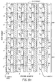
- the sensor architectures of Fig. 5a and 5b provide an additional capability over that already described. Because the column sample and hold circuits 150 provided at the pixel pitch, the two channel architecture can effectively store two rows of image data simultaneously. By timing the pixel output multiplexer two rows of sensor data can be stored with the color planes separated for efficient adjacent sample averaging. Referring to Figs. 5a , 7 , and 6e , it follows that R', B', Gr' and Gb' pixel values can be stored in the column circuit banks 80 as shown in Fig.
- R', B', Gr' and Gb' are the charge domain binned values for the paxel. These are denoted in Fig. 9 as the sum of two pixel values shown in each column circuit 150 location.
- Gr' and Gb' are stored in Bank 1 (80), and R' and B' are stored in bank 2 (80) as previously described. Now adjacent values of each color can be averaged in a pipelined manner as the sensor is read out.
- RGB per paxel 300 can also be easily converted selectively to YUV or YCC on chip in the digital domain. White balance and color correction could also be done simply for each paxel digitally. This is an advantage for direct output video for camera preview modes and other video modes.
- B10 and R01 1 become the B and R values for paxel 400 respectively, and the average of G00 and G11 become the G value for paxel 400.
- the readout is done in the same manner as full resolution mode, (for row 0, Gr is readout out through 1 ASP chain 110, R is readout through the other; for row 1, Gb is readout through 1 ASP chain and B is readout through the other).
- G channel averaging is done in the DSP block 140.
- Fig. 11 is a camera 500 for implementing all of the disclosed embodiments of the present invention.
Abstract
(a) a plurality of photodetectors arranged in an array of rows and columns that convert the light to a signal;
(b) means for reading out two or more samples of a same signal from each photodetector in at least one row, wherein the same signal is produced after a single integration period for all of the photodetectors in the at least one row;
(c) at least two signal storage banks comprised of individual signal storage elements; each of the at least two storage banks having enough individual storage elements to store the two or more signals from the at least one row of photodetectors in the array, wherein the two or more samples of the same signal are concurrently stored in different individual storage elements; and
(d) at least two select mechanisms which can direct signals from the plurality of photodetectors to any single or combination of the signal storage banks.
Description
- The present invention pertains to semiconductor based image sensors such as Active Pixel image sensors (APS), and Passive Pixel image sensors (PPS), and more particularly, to such APS and PPS with charge binning, high sensitivity, low noise, and parallel channel readout.
- APS and PPS are x-y addressable solid state imagers wherein each pixel contains both a photosensing element and a select element. For APS, each pixel also contains at least one other active circuit component. In both APS and PPS, incident illumination is converted to a signal (either a voltage or current signal). The signal represents the amount of light incident upon a pixel photosite. This signal is typically readout one row at time, and the signals for a given row are stored temporarily in a circuit associated with each column of the image sensor. This column circuit is typically constructed to fit into the size or pitch of the pixel.
- For many digital imaging applications, it is desirable to have a large number of pixels in a given size image sensor in order to increase the resolution of the image sensor. As the resolution requirement increases, the required pixel size decreases. As the pixel size decreases, several image sensor design and performance disadvantages are encountered. First, it becomes increasingly more difficult to construct a low noise column storage and readout circuit. Second, smaller pixels have lower sensitivity and can provide inadequate signal levels for low levels of illumination. Third, for a large number of pixels, the readout time will become longer. In many cases, a camera is required to produce video as well as still images.
- Typically the video rate desired is 30 frames per second. Prior art APS and PPS sensors have accomplished video rate data from large resolution sensors by windowing or sub-sampling of the image array using the x-y addressability feature of APS and PPS sensors. While this approach provides video rate data, it does so by selective readout of the small pixels and still has poor image quality in low light level environments, and produces aliasing image artifacts.
- Some APS and PPS sensors also include on sensor white balance by placing a programmable gain amplifier PGA in the readout path, which gain can change at a pixel data rate. For high resolution sensors, this has the disadvantage of requiring higher performance PGAs.
- From the foregoing discussion it should be apparent that there remains a need within the prior art for a high resolution, small pixel device that provides high readout rate, variable resolution while retaining low noise and high sensitivity.
- According to the present invention, there is provided a solution to problems of the prior art. In the present invention, an APS device with a selectable channel readout architecture is provided that enables small pixels and high resolution sensors, low noise column storage and readout circuitry, and adjacent same color sample averaging for high performance lower resolution readout.
- According to another embodiment of the present invention, the selectable channel readout architecture is employed with a shared amplifier pixel to provide selectable charge domain binning to further improve sensitivity and low light signal to noise performance.
- These and other aspects, objects, features and advantages of the present invention will be more clearly understood and appreciated from a review of the following detailed description of the preferred embodiments and appended claims, and by reference to the accompanying drawings.
- The invention has the following advantages. It provides for low noise, high sensitivity multiple resolution imaging from a single image sensor.
-
-
Fig. 1 is a block diagram for the sensor of a first embodiment of the present invention; -
Fig. 2 is an architecture diagram for the sensor of a first embodiment of the present invention; -
Fig. 3a is a block diagram for color difference readout; -
Fig. 3b is a timing diagram ofFig. 3a ; -
Fig. 4 is a schematic diagram of a four transistor active pixel; -
Fig. 5a is a block diagram for the sensor of a third embodiment of the present invention; -
Fig. 5b is an alternative embodiment ofFig. 5a with column banks at twice the pixel pitch; -
Fig. 6a is a block diagram for operation of the sensor shown inFig. 2 ; -
Fig. 6b first timing diagram ofFig. 6a ; -
Fig. 6c is a block diagram for operation of a second embodiment of the present invention; -
Fig. 6d is a timing diagram ofFig. 6c ; -
Fig. 6e is an operational block diagram for adjacent sample averaging operation of the sensor shown inFig. 5a ; -
Fig. 6f is a second operational block diagram for two row readout operation of the sensor shown inFig. 5a ; -
Fig. 7 is a schematic diagram of a pixel architecture of the present invention; -
Fig. 8a is a block diagram of a first reduced resolution readout operation of the present invention; -
Fig. 8b is a block diagram of a second reduced resolution readout operation of the present invention; -
Fig. 8c is an operational block diagram of reduced resolution readout operation of the present invention; -
Fig. 9 is a block diagram of a first reduced resolution readout operation of the third embodiment of the present invention; -
Fig. 10 is a block diagram of a second reduced resolution readout operation of the third embodiment of the present invention; and -
Fig. 11 is a camera for implementing all of the disclosed embodiments of the present invention. - The examples and diagrams provided in the description of the present invention represent one preferred embodiment of the present invention. Numerous other specific embodiments are feasible without departing from the scope of the present invention.
- Referring to
Fig. 1 , there is shown a top level block diagram of theimage sensor 10 of the present invention. The sensor array comprises a plurality ofpixels 20. Thepixels 20 can be any known APS or PPS x-y addressable pixel design. Two column circuit banks 80 (also referred to as storage regions), each comprising a plurality of column sample and hold circuits (not shown inFig. 1 ) are electrically connected to theoutput signal lines 90 of thesensor array 10. Two parallel analog signal processing (ASP) chains 110 (also referred to as readout regions) are respectively connected to eachcolumn circuit bank 80. An analog to digital converter (ADC) 120 is electrically connected to eachprocessing chain 110 for digitizing the signal. A 2:1digital multiplexer 130 is connected to both analog todigital converters 120 for selectively selecting the output from the two analog todigital converters 120. A digital signal processing (DSP) block 140 receives the signal from the multiplexer for further processing the signal. An interface is provided to operate and program various modes and specific parameters for the sensor. - Referring to
Fig. 2 , there is shown a block diagram of a plurality ofpixels 20 arranged in rows and columns, mated to a color filter (indicated by the letters R, G, B) for permitting each pixel to selectively receive light of a specific color determined by the bandpass of the color filter. In this figure the color filter pattern is a Bayer pattern, of red (R), green (G) and blue (B) bandpass filters. The R, G and B letters in each pixel denote the color filter associated with that pixel. In addition the letters E and O in each pixel denote the row and column identification as Even and Odd. For example the letters EO denote a pixel is in an even row and an odd column. For ease of detailed viewing, the diagram shows four rows and six columns, which are only a section of the imaging array and associated circuits. Twocolumn circuit banks 80 include a plurality of column sample and holdcircuits 150, which are electrically connected to the columns of pixels. More specifically, each bank comprises three column sample and holdcircuits 150 that are each electrically connected to two columns ofpixels 20 via a two-to-one pixeloutput analog multiplexer 160 that enables sample and hold of the signals from either of the two columns of pixels into either of the associated column circuits. As previously shown inFig. 1 , eachcolumn bank 80 is connected to an associatedASP chain 110 andADC 120. In this example, the column sample and holdcircuits 150 are constructed at twice the pixel pitch. This provides the advantage of being able to realize a low noise column sample and hold circuit for small pixels. The fixed pattern noise is improved by having more space for signal isolation and layout matching. Temporal noise of the column sample and holdcircuit 150 can be reduced by using larger capacitors and switches. The physical floor plan could be implemented with one bank at the top of the array and one bank on the bottom of the array, or both banks could also be stacked on a single side of the array. - As stated previously, one disadvantage with the prior art two channel architecture is offset and gain matching between the two channels. This will lead to green non-uniformity (GNU) artifacts.
- Still referring to the architecture in
Fig. 2 , the dashed lines with arrows within each column indicate which direction or bank of column circuits that the specific pixel is sampled and held in for a first preferred embodiment of the present invention. In this first configuration, all pixels of a particular color in a row are sent to a common column circuit bank. For example, all red pixels in even rows are sent tocolumn circuit bank 2, and all green pixels in even rows are sent tocolumn circuit bank 1. In odd rows, all blue pixels are sent tocolumn circuit bank 2 and all green pixels are sent tocolumn circuit bank 1. In this manner, the green color plane would go through asingle ASP chain 110 andADC 120, while red and blue would go through theother ASP chain 110 andADC 120. As a result, no offset or gain mismatch would occur between green pixels in the green-red row (Gr), and green pixels in the green-blue row (Gb). This is accomplished by timing of thepixel output multiplexer 130. This specific timing for this example is shown inFigs. 6a and6b . The signals Bank1_e and Bank1_o determine if the even and odd pixels respectively in a given row are sent tocolumn circuit bank 1. Bank2_e and Bank2_o serve the same purpose forcolumn circuit bank 2. For odd rows, Bank1_e is high, Bank1_o is low, Bank2_e is low and Bank2_o is high. For even rows, Bank1_e is low, Bank1_o is high, Bank2_e is high and Bank2_o is low. This color plane separation approach enabled by the present invention can mitigate the GNU issue. In general, the timing of the pixel output multiplexers can be used to send any pixel to either or both of the associated column sample and hold circuits. - Because of the color plane separation afforded by the selectable dual channel architecture, it is now possible to average like color signals in a pipelined manner because each column circuit bank and ASP chain contains samples of the same color for any given row. Also, by operating in this manner, a pixel rate White Balance (WB) Programmable Gain Amplifier (PGA) is not needed since for any given row, each
ASP chain 110 contains signals from a single color plane. In this case the WB PGA must change at a line rate and alternate between Gr and Gb forASP chain 1, and R and B forASP chain 2.ASP chain 1 andchain 2 are identical, and operate at one half the final pixel output data rate. - In another configuration of this same architecture, a color difference readout can be provided. The color difference readout operation will be described using the four transistor active pixel shown in
Fig. 4 , although the other pixel architectures can be used without departing from the scope of the invention. Referring to the sensor block diagram and timing diagram inFigs. 3a and3b , color difference readout is accomplished in the following manner. Referring to bothFigs. 3a ,3b , and4 , after integration is completed, readout of therow 1 commences after reset of the floatingdiffusions 190 of the pixels in that row, (a green-red row in this example). The reset level of the floatingdiffusion 190 in the green pixel is then stored as the reference level in onecolumn circuit bank 80. This is referred to as Resetg. Next the signal in thephotodiode 170 is transferred to the floatingdiffusion 190 for all pixels in the row. The signal level on the floatingdiffusion 190 in the red pixels is now stored as the reference level in the secondcolumn circuit bank 80. This voltage level stored is R + Resetr. Next the signal level of the floatingdiffusion 190 in the green pixel is stored as the signal level in both column circuit banks. This is G + Resetg. Readout of the stored signal now commences. Onecolumn bank 80 produces a true correlated double sample readout of the green signal level as shown inequation 1.
- The other column circuit bank provides a color difference signal readout as shown in
equation 2.
This process repeats for all rows in the sensor. - Another embodiment of the selectable dual channel sensor architecture of the present invention is shown in
Figs. 6c and6d . The analog multiplexers (160 in the previous Figures) are eliminated and separate control of sample and hold signals for each bank are provided. These signals are labeled SHS_e and SHS_o for sample and hold signal even and odd respectively, and SHR_e and SHR_o for sample and hold reference even and odd respectively. These are provided separately forcolumn circuit banks 1 and 2 (80) and denoted inFigs. 6c and6d accordingly. The analogous timing forFigs. 6a and6b with this architecture is shown inFigs. 6c and6d . In general the timing of the bank sample and hold signals can be used to send any pixel to either or both of the associated column sample and holdcircuits 150. - An alternate sensor architecture is shown in
Figs. 5a and5b . In the case ofFig. 5a , there are two banks of column sample and holdcircuits 80, but the column sample and holdcircuits 150 are constructed at the pixel pitch. Thepixel output multiplexer 160 is now a 2:2 configuration where the odd and even pixel in a given row can be sent to one of two, or both column sample and holdcircuits 150 associated with thatmultiplexer 160. Details ofmultiplexer 160 are not shown and can be any configuration known in the art.Fig. 5b is electrically equivalent toFig. 5a , except that thecolumn banks 80 are split into twosub-banks 150 that are constructed at twice the pixel pitch. This stacked or staggered approach shown inFig. 5b retains the advantages of a wider column circuit as described for the architecture ofFig. 2 . - The same color plane separation can be accomplished with the two channel sensor architectures of
Figs. 5a and5b in a similar manner as described for the sensor architecture ofFigs. 2 ,3a , and3b . The sensor architectures ofFigs. 5a and5b provide an additional capability over that already described. Because the column sample and holdcircuits 150 are built at the pixel pitch, the two channel architecture can effectively store and readout two samples of each pixel in a single row of image data simultaneously. By timing thepixel output multiplexer 160, two samples of the pixel value in each row of sensor data can be stored with the color planes separated for efficient adjacent sample averaging. This is shown inFig. 6e . Again the operation is described in the context of the pixel shown inFig. 4 in a rolling shutter mode. Other pixel architectures and modes of operations can be used without departing from the scope of the invention. After integration ends, sample and hold ofrow 0, an even row, commences. Each Gr pixel signal level is stored in two adjacent column locations of column circuit bank 1 (80) by using thepixel output multiplexer 160 to connect the Gr pixel output to both of the associated column sample and holdcircuits 150 in bank 1 (80). Each of the G pixels stored in the respective column sample and hold circuit is labeled as G0X, where 0 denotes row zero and X denotes the column number in that row. As shown inFig. 6e each G pixel in the row gets stored in two adjacent column locations in column circuit bank 1 (80). Similarly each of the R signal values inrow 0 is sampled and held in two adjacent column sample and holdcircuits 150 in bank 2 (80). Now the two banks (80) can be read out in parallel and the two adjacent stored signals from a single pixel can be averaged to create a lower noise value. The average is most easily accomplished in the digital domain after analog to digital conversion. The process is repeated for the next row, an odd row, where two samples of Gb are stored in bank 1 (80), and two adjacent samples for each B are stored in bank 2 (80). In general, this approach can be employed with n-sample and holds connected to a single pixel to provide n-sample averaging. - The same color plane separation afforded by the two channel sensor architecture of
Figs. 2 ,6c , and6d can also be accomplished with the two channel sensor architecture ofFigs. 5a and5b by storage and readout of two rows in parallel. Referring toFig. 6f , after integration ends sample and hold ofrow 0, an even row, commences. Each Gr pixel signal level is stored in even column locations of column circuit bank 1 (80) by using thepixel output multiplexer 160 to connect the Gr pixel output to the even column locations of the associated column sample and holdcircuits 150 in bank 1 (80). Similarly each of the R pixel signal values is sampled and held in the odd column sample and holdcircuits 150 in bank 2 (80).Next row 1, an odd row is sampled and held. Each Gb pixel signal level is stored in odd column locations of column circuit bank 1 (80) by using thepixel output multiplexer 160 to connect the Gb pixel output to odd column locations of the associated column sample and holdcircuits 150 in bank 1 (80). Similarly each of the B pixel signal values is sampled and held in the even column sample and holdcircuits 150 in bank 2 (80). Now the two banks (80) can be read out in parallel. This is shown inFig. 6f by placement of specific R, G and B pixels in the column circuits with a value of Cxy, where C denotes the color, x denotes the row and y denotes the column. For example B10 is the blue pixel inrow 1 andcolumn 0. This process is repeated for each group of two rows in the array. By storage and readout in this manner, a 2x2 region of the array is always available in the digital domain and this can be utilized for on-chip pipelined color processing. - It should be noted that any pixel architecture can be used in conjunction with this selectable two channel storage and readout architectures described in the present invention without departing from the scope of the invention. Further the dual channel concept can be extended to multiple channels with the ability to store and readout any pixel in any bank.
- Further advantages of the selectable multi-channel sensor architecture can be realized by use of a specific pixel architecture. A shared amplifier pixel can be employed with the selectable two-channel sensor architecture, to enable charge domain binning and adjacent sample averaging to provide higher sensitivity and lower noise for cases where lower resolution still images or low light, lower resolution video is desired. One example of an envisioned embodiment of the shared pixel architecture is shown in
Fig. 7 . - Referring to
Fig. 7 , there is shown a schematic drawing of a shared amplifier pixel of the present invention. This pixel architecture enables charge domain binning of the same color pixels, as well as charge domain binning of all pixels that share the same amplifier. Although this pixel is used as a preferred embodiment of the present invention, other pixel architectures can be employed for both charge domain binning, and for use in the selectable dual channel storage and readout architecture. Fourpixels 20 are shown in the drawing. These fourpixels 20 are arranged in a column, such that eachpixel 20 is associated with a given row. This set of fourpixels 20 comprises a sensor array unit cell. Each pixel comprises aphotodetector 170, and atransfer gate 180. The floatingdiffusion 190,reset transistor 200 with areset gate 210, sourcefollower input transistor 220, row select transistor 230, andoutput signal line 240 are shared between the four pixels. A plurality of unit cells comprises the sensor array. Other specific embodiments are possible and readily apparent to someone skilled in the art. - There are four TG signals and one RG signal associated with a single row select line. This will be referred to as a four-shared pixel. As a result of the four-shared pixel, four photodiodes share the same floating diffusion node. Since the color pattern within a column is alternating colors, (e.g. G,R or B,G), photoelectrons collected in the same color photodiode can be summed or binned on the common floating diffusion (FD) by transferring of charge from the appropriate sets of photodiodes onto the FD. This will increase the effective responsivity or sensitivity of the sensor since the number of electrons collected for any given light level or integration time will be doubled. In addition, for very low light conditions where color information is not absolutely necessary, all four photodiode signals can be binned onto the common FD, further increasing sensitivity.
- In the first example a 16x resolution reduction of the full resolution image is accomplished For example, a two megapixel sensor of 1632 x 1224 pixels would be reduced down to an image of 408 x 306. The resolution reduction is done by combining signals from a four pixel by four pixel area into a single new picture element referred to as a
paxel 300. Thispaxel 300 is shown inFig. 8a . Referring toFigs. 2 ,7 ,8a and8c , the rolling shutter start is applied to even and odd row pairs in the four rows of thepaxel 300, so that the even and odd rows in thepaxel 300 will have the same integration time. At the end of the desired integration readout begins for the even rows by reset of theFD 190 by pulsingRG 210 and storage of the reset level in the column sample and holdcircuit 80, then pulsingTG 180 to transfer charge from thePD 170 to theFD 190 followed by storage of the signal + reset level in the column sample and hold circuit. This is done forrow RG 210 is pulsed, reset level is sampled and held, TG0 (310) and TG2 (320) are pulsed simultaneously, this signal level is then sampled and held). At this point we have the two Green pixels binned on the floating diffusion of the even columns, and the two Red pixels binned on the floatingdiffusion 190 of the odd columns. This is denoted inFig. 8c as the sum of two pixel values located in the respective column sample and holdcircuit 150. The Green signals will be pipelined through one ASP channel, and the Red signals will be pipelined through the other ASP channel, as described in the dual channel architecture operation. - Now a key advantage of the dual channel architecture column can be employed. Because the signals stored in the respective ASP channels are the same color, adjacent signal samples can be directly and simply averaged in a pipelined manner to create a single value from the two adjacent color values in the 4x4 paxel. For example, after the ADC's 120 the two adjacent samples of each color, (2-Gr's and 2-R's), are averaged digitally and output as a single 10 bit R value and Gr value. This is shown in
Fig. 8c . In this case the R and Gr value are actually derived from four individual pixels, two pixels binned in the charge domain and two binned values averaged in the digital domain. Thus sensitivity is increased and noise is reduced. - Next the odd rows in the
paxel 300 are read out in a similar manner, (same as even rows except TG1 315 and TG3 325 are pulsed simultaneously). The Blue pixels are binned in the even columns and the Gb pixels are binned in the odd columns. The Gb values are sampled and held and then pipelined through the same channel as Gr, while the Blue values are sampled and held and then pipelined through the same channel as the Red pixels. The two adjacent values of B and Gb can now be digitally averaged, and single 10 bit values of B and Gb can be output from the sensor. The Gr and Gb values can be averaged off chip if desired to further reduce noise. - This approach has several advantages over the prior art sub-sampling method of APS devices. First, sensitivity is increased. Second, noise is reduced. This leads to a higher dynamic range. Additionally, aliasing artifacts caused by sub-sampling are not produced.
- This same charge domain binning and voltage or digital domain adjacent sample averaging can be utilized with the sensor architecture of
Figs. 5a and5b . The sensor architectures ofFig. 5a and5b provide an additional capability over that already described. Because the column sample and holdcircuits 150 provided at the pixel pitch, the two channel architecture can effectively store two rows of image data simultaneously. By timing the pixel output multiplexer two rows of sensor data can be stored with the color planes separated for efficient adjacent sample averaging. Referring toFigs. 5a ,7 , and6e , it follows that R', B', Gr' and Gb' pixel values can be stored in thecolumn circuit banks 80 as shown inFig. 9 , where R', B', Gr' and Gb' are the charge domain binned values for the paxel. These are denoted inFig. 9 as the sum of two pixel values shown in eachcolumn circuit 150 location. Gr' and Gb' are stored in Bank 1 (80), and R' and B' are stored in bank 2 (80) as previously described. Now adjacent values of each color can be averaged in a pipelined manner as the sensor is read out. - Additionally, since all color values are now available at the same time, no interpolation is required to get an RGB value per 4x4 paxel. The RGB per
paxel 300 can also be easily converted selectively to YUV or YCC on chip in the digital domain. White balance and color correction could also be done simply for each paxel digitally. This is an advantage for direct output video for camera preview modes and other video modes. - Referring to
Figs. 10 and8b , a 4x reduction in resolution can be accomplished. B10 andR01 1 become the B and R values forpaxel 400 respectively, and the average of G00 and G11 become the G value forpaxel 400. The readout is done in the same manner as full resolution mode, (forrow 0, Gr is readout out through 1ASP chain 110, R is readout through the other; forrow 1, Gb is readout through 1 ASP chain and B is readout through the other). G channel averaging is done in theDSP block 140. -
Fig. 11 is acamera 500 for implementing all of the disclosed embodiments of the present invention. - The foregoing discussion describes the embodiments most preferred by the inventor. Numerous variations will be readily apparent to those skilled in the relevant art. Therefore, the scope of the invention should be measured not by the disclosed embodiments but by the appended claims.
- The invention has been described with reference to a preferred embodiment. However, it will be appreciated that variations and modifications can be effected by a person of ordinary skill in the art without departing from the scope of the invention.
-
-
Item 1. An image sensor comprising:- (a) a plurality of light measuring elements arranged in an array and at least a portion of the elements have a color filter mated with the light receiving elements which permits selective color reception by the light measuring elements;
- (b) a plurality of floating diffusions respectively mated with the plurality of light receiving elements; and
- c) an output structure electrically connected to two or more of the floating diffusions; wherein the at least two light receiving elements receiving the same color are transferred to the output structure substantially simultaneously.
-
Item 2. The image sensor as initem 1, wherein all the light receiving electrically connected to the same output structure are transferred to the output structure substantially simultaneously. -
Item 3. A camera comprising:- (a) an image sensor comprising:
- (a1) a plurality of light measuring elements arranged in an array and at least a portion of the elements have a color filter mated with the light receiving elements which permits selective color reception by the light measuring elements;
- (a2) a plurality of floating diffusions respectively mated with the plurality of light receiving elements; and
- (a3) an output structure electrically connected to two or more of the floating diffusions; wherein the at least two light receiving elements receiving the same color are transferred to the output structure substantially simultaneously.
- (a) an image sensor comprising:
-
Item 4. The camera as initem 3, wherein all the light receiving electrically connected to the same output structure are transferred to the output structure substantially simultaneously. -
Item 5. An image sensor comprising:- (a) a plurality of light measuring elements a portion of which have a color filter mated with the light receiving elements, and the light receiving elements are arranged in an array;
- (b) a plurality of floating diffusions respectively mated with the plurality of light receiving elements;
- (c) two column circuits used to store the signal from the light receiving elements one row at a time; and
- (d) a select switch used to control which column circuit a particular signal from a light receiving is stored.
-
Item 6. The image sensor as initem 5, wherein substantially all of the same colors are transferred to the same column circuit. -
Item 7. The image sensor as initem 6, wherein adjacent samples in each column circuit are averaged. -
Item 8. A camera comprising:- (a) an image sensor comprising:
- (a1) a plurality of light measuring elements a portion of which have a color filter mated with the light receiving elements, and the light receiving elements are arranged in an array;
- (a2) a plurality of floating diffusions respectively mated with the plurality of light receiving elements;
- (a3) two column circuits used to store the signal from the light receiving elements one row at a time; and
- (a4) a select switch used to control which column circuit a particular signal from a light receiving is stored.
- (a) an image sensor comprising:
-
Item 9. The camera as initem 8, wherein substantially all of the same colors are transferred to the same column circuit. -
Item 10. The camera as initem 9, wherein adjacent samples in each column circuit are averaged. - Item 11. An x-y addressable image sensor comprising:
- (a) a plurality of light measuring elements arranged in an array of rows and columns that convert the light to a signal;
- (b) at least two signal storage banks comprised of individual signal storage elements; the at least two storage banks having enough individual storage elements to store the signals from at least one row of light measuring elements in the array; and
- (c) at least two select mechanisms which can direct signals from the plurality of light measuring elements to any single or combination of the signal storage banks.
-
Item 12. The image sensor as in item 11 further comprising a plurality of color filters mated with the plurality of light measuring elements, and the select mechanism is used to send signals from the light measuring elements mated to a single color filter type to a desired signal storage bank such that, for any given row, a single signal storage bank contains signals from a single color type. -
Item 13. The image sensor as initem 12 wherein the color filter is a Bayer pattern in which a color of a single type is sent to only one of the two signal storage banks. - Item 14. The image sensor as in
item 13, wherein the single color type sent to only one of the storage regions is green. - Item 15. The image sensor as in item 11, wherein the individual signal storage elements in the signal storage banks are larger than light measuring element pitch.
- Item 16. The image sensor as in item 11, wherein the at least two select mechanisms direct signals from the each of the plurality of light measuring elements to both signal storage banks.
- Item 17. The image sensor as in item 11 further comprising a plurality of signal storage banks and the at least two select mechanisms direct signals to multiple signal storage banks.
-
Item 18. The image sensor as in item 11, wherein a single pixel can be directed to multiple single storage elements within any signal storage bank. - Item 19. The image sensor of
item 18, wherein adjacent signals from the light measuring elements in the adjacent signal storage elements are averaged to produce a single value. -
Item 20. The image sensor as in item 11, wherein a single pixel can be directed to adjacent individual signal storage elements within any signal storage bank. -
Item 21. The image sensor ofitem 20, wherein adjacent signals from the light measuring elements in the adjacent signal storage elements are averaged to produce a single value. -
Item 22. An image sensor comprising:- (a) a plurality of light measuring elements each having a photodetector and a transfer mechanism; and
- (b) a plurality of charge to voltage conversion regions; wherein at least two adjacent light measuring elements share a charge to voltage conversion region;
- wherein charge of adjacent light measuring elements is combined in the shared charge to voltage conversion region.
-
Item 23. The image sensor as initem 22, wherein the timing selectively combines charge from light measuring elements with a similar color filter array element. -
Item 24. The image sensor as initem 22, wherein charge of adjacent light measuring elements is substantially simultaneously transferred to the shared charge to voltage conversion region - Item 25. The image sensor as in
item 22, wherein the charge of all adjacent light measuring elements associated with a common charge to voltage conversion regions is transferred to the shared charge to voltage conversion region to form a single voltage signal associated with all of the adjacent light measuring elements. - Item 26. A camera comprising:
- an x-y addressable image sensor comprising:
- (a) a plurality of light measuring elements arranged in an array of rows and columns that convert the light to a signal;
- (b) at least two signal storage banks comprised of individual signal storage elements; the at least two storage banks having enough individual storage elements to store the signals from at least one row of light measuring elements in the array; and
- (c) at least two select mechanisms which can direct signals from the plurality of light measuring elements to any single or combination of the signal storage banks.
- an x-y addressable image sensor comprising:
- Item 27. The camera as in item 26 further comprising a plurality of color filters mated with the plurality of light measuring elements, and the select mechanism is used to send signals from the light measuring elements mated to a single color filter type to a desired signal storage bank such that, for any given row, a single signal storage bank contains signals from a single color type.
- Item 28. The camera as in item 27 wherein the color filter is a Bayer pattern in which a color of a single type is sent to only one of the two signal storage banks.
- Item 29. The camera as in item 28, wherein the single color type sent to only one of the storage regions is green.
-
Item 30. The camera as in item 26, wherein the individual signal storage elements in the signal storage banks are larger than light measuring element pitch. -
Item 31. The camera as in item 26, wherein the at least two select mechanisms direct signals from the each of the plurality of light measuring elements to both signal storage banks. -
Item 32. The camera as in item 26 further comprising a plurality of signal storage banks and the at least two select mechanisms direct signals to multiple signal storage banks. -
Item 33. The camera as in item 26, wherein a single pixel can be directed to multiple single storage elements within any signal storage bank. -
Item 34. The camera as initem 33, wherein adjacent signals from the light measuring elements in the adjacent signal storage elements are averaged to produce a single value. - Item 35. The camera as in item 26, wherein a single pixel can be directed to adjacent individual signal storage elements within any signal storage bank.
- Item 36. The camera as in item 35, wherein adjacent signals from the light measuring elements in the adjacent signal storage elements are averaged to produce a single value.
- Item 37. A camera comprising:
- an image sensor comprising:
- (a) a plurality of light measuring elements each having a photodetector and a transfer mechanism; and
- (b) a plurality of charge to voltage conversion regions; wherein at least two adjacent light measuring elements share a charge to voltage conversion region;
- wherein charge of adjacent light measuring elements is combined in the shared charge to voltage conversion region.
- an image sensor comprising:
- Item 38. The camera as in item 37, wherein the timing selectively combines charge from light measuring elements with a similar color filter array element.
- Item 39. The camera as in item 37, wherein charge of adjacent light measuring elements is substantially simultaneously transferred to the shared charge to voltage conversion region
-
Item 40. The camera as in item 37, wherein the charge of all adjacent light measuring elements associated with a common charge to voltage conversion regions is transferred to the shared charge to voltage conversion region to form a single voltage signal associated with all of the adjacent light measuring elements. -
- 10
- image sensor (or sensor array)
- 20
- pixels
- 80
- column circuit banks (or storage regions)
- 90
- output signal lines
- 110
- analog signal processing (ASP) chains (or readout regions)
- 120
- analog to digital converter (ADC)
- 130
- 2:1 digital multiplexer/pixel output multiplexer
- 140
- digital signal processing (DSP) block
- 150
- column sample and hold circuits
- 160
- two-to-one pixel output analog multiplexer
- 170
- photodiode/photodetector
- 180
- transfer gate
- 190
- floating diffusion
- 200
- reset transistor
- 210
- reset gate
- 220
- source following input transistor
- 230
- row select transistor
- 240
- output signal line
- 300
- paxel
- 310
- TG0
- 315
- TG1
- 320
- TG2
- 325
- TG3
- 400
- paxel
Claims (6)
- An x-y addressable image sensor comprising:(a) a plurality of photodetectors arranged in an array of rows and columns that convert the light to a signal;(b) means for reading out two or more samples of a same signal from each photodetector in at least one row, wherein the same signal is produced after a single integration period for all of the photodetectors in the at least one row;(c) at least two signal storage banks comprised of individual signal storage elements; each of the at least two storage banks having enough individual storage elements to store the two or more signals from the at least one row of photodetectors in the array, wherein the two or more samples of the same signal are concurrently stored in different individual storage elements; and(d) at least two select mechanisms which can direct signals from the plurality of photodetectors to any single or combination of the signal storage banks.
- The x-y addressable image sensor as in claim 1, wherein the image sensor is included in a camera.
- The x-y addressable image sensor as in claim 1, wherein the individual signal storage elements in the at least two signal storage banks are larger than photodetector pitch.
- A method for operating an x-y addressable image sensor that includes at least two storage banks comprised of individual storage elements each of the at least two storage banks having enough individual storage elements to store signals from at least one row of photodetectors, the method comprising:capturing an image using a single integration period for all of the photodetectors in at least one row;after the single integration period, reading out two or more samples of the same signal for each photodetector in the at least one row; andconcurrently storing the two or more samples of the same signal in respective storage elements in the at least two storage banks.
- The method as in claim 4, further comprising:for each photodetector in the at least one row, reading out the two or more samples of the same signal from the respective storage elements; andaveraging the two or more samples to produce an averaged signal.
- The method as in claim 4, wherein the image sensor further includes a plurality of color filters mated with the plurality of photodetectors and the method further comprises directing signals from the photodetectors mated to color filters representing a particular color to a common storage bank.
Applications Claiming Priority (2)
| Application Number | Priority Date | Filing Date | Title |
|---|---|---|---|
| US10/620,060 US7859581B2 (en) | 2003-07-15 | 2003-07-15 | Image sensor with charge binning and dual channel readout |
| EP04777398A EP1656799A2 (en) | 2003-07-15 | 2004-07-01 | Image sensor with charge binning |
Related Parent Applications (2)
| Application Number | Title | Priority Date | Filing Date |
|---|---|---|---|
| EP04777398.1 Division | 2004-07-01 | ||
| EP04777398A Division EP1656799A2 (en) | 2003-07-15 | 2004-07-01 | Image sensor with charge binning |
Publications (3)
| Publication Number | Publication Date |
|---|---|
| EP2323409A2 true EP2323409A2 (en) | 2011-05-18 |
| EP2323409A3 EP2323409A3 (en) | 2013-08-28 |
| EP2323409B1 EP2323409B1 (en) | 2017-08-23 |
Family
ID=34062702
Family Applications (2)
| Application Number | Title | Priority Date | Filing Date |
|---|---|---|---|
| EP04777398A Withdrawn EP1656799A2 (en) | 2003-07-15 | 2004-07-01 | Image sensor with charge binning |
| EP11156524.8A Active EP2323409B1 (en) | 2003-07-15 | 2004-07-01 | Image sensor with charge binning |
Family Applications Before (1)
| Application Number | Title | Priority Date | Filing Date |
|---|---|---|---|
| EP04777398A Withdrawn EP1656799A2 (en) | 2003-07-15 | 2004-07-01 | Image sensor with charge binning |
Country Status (7)
| Country | Link |
|---|---|
| US (1) | US7859581B2 (en) |
| EP (2) | EP1656799A2 (en) |
| JP (1) | JP4611296B2 (en) |
| KR (2) | KR101159014B1 (en) |
| CN (2) | CN101778193B (en) |
| TW (1) | TWI358942B (en) |
| WO (1) | WO2005011264A2 (en) |
Cited By (1)
| Publication number | Priority date | Publication date | Assignee | Title |
|---|---|---|---|---|
| US20180190687A1 (en) * | 2015-07-03 | 2018-07-05 | Sony Semiconductor Solutions Corporation | Image sensor, image processing method, and electronic device |
Families Citing this family (72)
| Publication number | Priority date | Publication date | Assignee | Title |
|---|---|---|---|---|
| US6239456B1 (en) | 1998-08-19 | 2001-05-29 | Photobit Corporation | Lock in pinned photodiode photodetector |
| DE19947536A1 (en) * | 1999-10-02 | 2001-04-05 | Philips Corp Intellectual Pty | Sensor array read-out method e.g. for diagnostic X-ray imaging, has controlled switches between adjacent addressing lines and adjacent read-out lines |
| US7492391B1 (en) * | 2003-07-14 | 2009-02-17 | Arecont Vision, Llc. | Wide dynamic range network camera |
| US20050062866A1 (en) * | 2003-09-23 | 2005-03-24 | Ang Lin Ping | Multiplexed pixel column architecture for imagers |
| US11282891B2 (en) | 2003-11-26 | 2022-03-22 | Samsung Electronics Co., Ltd. | Image sensor with a gated storage node linked to transfer gate |
| US7443437B2 (en) | 2003-11-26 | 2008-10-28 | Micron Technology, Inc. | Image sensor with a gated storage node linked to transfer gate |
| US7087883B2 (en) * | 2004-02-04 | 2006-08-08 | Omnivision Technologies, Inc. | CMOS image sensor using shared transistors between pixels with dual pinned photodiode |
| KR100871687B1 (en) * | 2004-02-11 | 2008-12-05 | 삼성전자주식회사 | Solid state image sensing device improving display quality in sub-sampling mode and driving method thereof |
| JP4107269B2 (en) * | 2004-02-23 | 2008-06-25 | ソニー株式会社 | Solid-state imaging device |
| KR100871688B1 (en) * | 2004-02-27 | 2008-12-08 | 삼성전자주식회사 | Solid State Imaging Device and Driving Method Therefor |
| JP2005312025A (en) * | 2004-04-21 | 2005-11-04 | Magnachip Semiconductor Ltd | Cmos image sensor capable of conducting high-speed analog signal processing |
| JP2005318544A (en) * | 2004-04-26 | 2005-11-10 | Magnachip Semiconductor Ltd | Cmos image sensor capable of high-speed processing of analog signal |
| US20050237407A1 (en) * | 2004-04-26 | 2005-10-27 | Chang-Min Bae | CMOS image sensor for processing analog signal at high speed |
| JP4971586B2 (en) | 2004-09-01 | 2012-07-11 | キヤノン株式会社 | Solid-state imaging device |
| JP4306603B2 (en) * | 2004-12-20 | 2009-08-05 | ソニー株式会社 | Solid-state imaging device and driving method of solid-state imaging device |
| KR100657863B1 (en) | 2005-02-07 | 2006-12-14 | 삼성전자주식회사 | Cmos active pixel sensor using fingered type source follower transistor |
| JP4969792B2 (en) * | 2005-04-14 | 2012-07-04 | 浜松ホトニクス株式会社 | Solid-state imaging device |
| US7238926B2 (en) * | 2005-06-01 | 2007-07-03 | Eastman Kodak Company | Shared amplifier pixel with matched coupling capacitances |
| US7705900B2 (en) * | 2005-06-01 | 2010-04-27 | Eastman Kodak Company | CMOS image sensor pixel with selectable binning and conversion gain |
| US8253214B2 (en) * | 2005-06-02 | 2012-08-28 | Omnivision Technologies, Inc. | CMOS shared amplifier pixels with output signal wire below floating diffusion interconnect for reduced floating diffusion capacitance |
| TWI310987B (en) * | 2005-07-09 | 2009-06-11 | Samsung Electronics Co Ltd | Image sensors including active pixel sensor arrays |
| US7541628B2 (en) | 2005-07-09 | 2009-06-02 | Samsung Electronics Co., Ltd. | Image sensors including active pixel sensor arrays |
| KR100787938B1 (en) * | 2005-07-15 | 2007-12-24 | 삼성전자주식회사 | Cmos image sensor of shared active pixel sensor structure and driving method |
| JP4827524B2 (en) * | 2005-12-26 | 2011-11-30 | キヤノン株式会社 | Imaging device |
| US7427736B2 (en) * | 2006-03-23 | 2008-09-23 | Micron Technology, Inc. | Method and apparatus for providing a rolling double reset timing for global storage in image sensors |
| JP5123601B2 (en) * | 2006-08-31 | 2013-01-23 | キヤノン株式会社 | Photoelectric conversion device |
| US7773138B2 (en) * | 2006-09-13 | 2010-08-10 | Tower Semiconductor Ltd. | Color pattern and pixel level binning for APS image sensor using 2×2 photodiode sharing scheme |
| TWI345910B (en) * | 2006-10-02 | 2011-07-21 | Novatek Microelectronics Corp | Cmos image sensor for high-speed operation |
| US7768562B2 (en) * | 2006-10-10 | 2010-08-03 | Micron Technology, Inc. | Method, apparatus and system providing imager vertical binning and scaling using column parallel sigma-delta digital conversion |
| US8013920B2 (en) | 2006-12-01 | 2011-09-06 | Youliza, Gehts B.V. Limited Liability Company | Imaging system for creating an image of an object |
| US8031249B2 (en) * | 2007-01-11 | 2011-10-04 | Micron Technology, Inc. | Missing pixel architecture |
| US8009211B2 (en) * | 2007-04-03 | 2011-08-30 | Canon Kabushiki Kaisha | Image sensing apparatus and image capturing system |
| US20090033389A1 (en) * | 2007-08-03 | 2009-02-05 | Abadeer Wagdi W | Micro-phase adjusting and micro-phase adjusting mixer circuits designed with standard field effect transistor structures |
| US7755121B2 (en) * | 2007-08-23 | 2010-07-13 | Aptina Imaging Corp. | Imagers, apparatuses and systems utilizing pixels with improved optical resolution and methods of operating the same |
| JP4386118B2 (en) | 2007-08-31 | 2009-12-16 | ソニー株式会社 | Imaging circuit |
| US8144226B2 (en) | 2008-01-04 | 2012-03-27 | AltaSens, Inc | Two-by-two pixel structure in an imaging system-on-chip |
| US8743247B2 (en) * | 2008-01-14 | 2014-06-03 | International Business Machines Corporation | Low lag transfer gate device |
| US8227844B2 (en) * | 2008-01-14 | 2012-07-24 | International Business Machines Corporation | Low lag transfer gate device |
| US7999870B2 (en) * | 2008-02-01 | 2011-08-16 | Omnivision Technologies, Inc. | Sampling and readout of an image sensor having a sparse color filter array pattern |
| US8081247B2 (en) * | 2008-06-18 | 2011-12-20 | Omnivision Technologies, Inc. | Partial row readout for image sensor |
| EP2154879A1 (en) * | 2008-08-13 | 2010-02-17 | Thomson Licensing | CMOS image sensor with selectable hard-wired binning |
| JP2010098516A (en) * | 2008-10-16 | 2010-04-30 | Sony Corp | Imaging element and control method thereof, and camera |
| TWI520030B (en) | 2009-05-21 | 2016-02-01 | 原相科技股份有限公司 | Cmos image sensor and method of operating the same |
| CN101924944B (en) | 2009-06-15 | 2013-06-05 | 华为技术有限公司 | Selection method and information providing method and devices of scalable video coding operating point |
| WO2011053711A1 (en) * | 2009-10-30 | 2011-05-05 | Invisage Technologies, Inc. | Systems and methods for color binning |
| CN102055919B (en) * | 2009-11-04 | 2012-11-07 | 原相科技股份有限公司 | Complementary metal oxide semiconductor (CMOS) image sensor and operation method thereof |
| KR101198249B1 (en) * | 2010-07-07 | 2012-11-07 | 에스케이하이닉스 주식회사 | Column circuit and pixel binning circuit of image sensor |
| JP5500007B2 (en) * | 2010-09-03 | 2014-05-21 | ソニー株式会社 | Solid-state imaging device and camera system |
| US9191582B1 (en) * | 2011-04-29 | 2015-11-17 | Bae Systems Information And Electronic Systems Integration Inc. | Multi-mode high speed sensor |
| WO2013009428A2 (en) * | 2011-07-14 | 2013-01-17 | Analog Devices, Inc. | Image sensor with a charge-based readout circuit |
| JP2013150116A (en) * | 2012-01-18 | 2013-08-01 | Canon Inc | Imaging apparatus and driving method of imaging apparatus |
| KR102087225B1 (en) * | 2013-05-30 | 2020-03-11 | 에스케이하이닉스 주식회사 | Image sensing device |
| KR20150014007A (en) * | 2013-07-25 | 2015-02-06 | 삼성전자주식회사 | Image sensor and imaging device including the same |
| KR102084543B1 (en) * | 2013-09-25 | 2020-03-04 | 엘지디스플레이 주식회사 | Apparatus for driving touch screen |
| JP6180882B2 (en) * | 2013-10-31 | 2017-08-16 | ソニーセミコンダクタソリューションズ株式会社 | Solid-state imaging device, signal processing device, and electronic device |
| US9277136B2 (en) | 2013-11-25 | 2016-03-01 | Samsung Electronics Co., Ltd. | Imaging systems and methods with pixel sensitivity adjustments by adjusting demodulation signal |
| JP6369015B2 (en) * | 2013-11-28 | 2018-08-08 | 株式会社ニコン | Imaging device |
| KR101541123B1 (en) * | 2013-11-29 | 2015-08-03 | (주)실리콘화일 | Image data output appratus for image signal processor |
| US9578267B2 (en) * | 2013-12-23 | 2017-02-21 | Alexander Krymski | Cameras and methods with data processing, memories, and an image sensor with multiple data ports |
| US9741755B2 (en) | 2014-12-22 | 2017-08-22 | Google Inc. | Physical layout and structure of RGBZ pixel cell unit for RGBZ image sensor |
| US9871065B2 (en) | 2014-12-22 | 2018-01-16 | Google Inc. | RGBZ pixel unit cell with first and second Z transfer gates |
| US9425233B2 (en) | 2014-12-22 | 2016-08-23 | Google Inc. | RGBZ pixel cell unit for an RGBZ image sensor |
| KR101631061B1 (en) * | 2015-02-05 | 2016-06-16 | 동국대학교 산학협력단 | CMOS image sensor having multi-mode resolution |
| JP2017085065A (en) * | 2015-10-30 | 2017-05-18 | ルネサスエレクトロニクス株式会社 | Semiconductor device and manufacturing method of the same |
| CN107018297B (en) * | 2015-11-27 | 2020-10-13 | 钰立微电子股份有限公司 | Image acquisition device |
| US10313610B2 (en) | 2016-04-14 | 2019-06-04 | Qualcomm Incorporated | Image sensors with dynamic pixel binning |
| US10313609B2 (en) | 2016-04-14 | 2019-06-04 | Qualcomm Incorporated | Image sensors having pixel-binning with configurable shared floating diffusion |
| US10362255B2 (en) | 2017-02-09 | 2019-07-23 | Semiconductor Components Industries, Llc | Multi-conversion gain pixel configurations |
| JP6918517B2 (en) * | 2017-02-21 | 2021-08-11 | キヤノン株式会社 | Image sensor, its control method, and image sensor |
| JP6726160B2 (en) * | 2017-12-22 | 2020-07-22 | キヤノン株式会社 | Imaging device, imaging system, signal processing device, and signal processing method |
| KR20210076238A (en) * | 2019-12-13 | 2021-06-24 | 삼성전자주식회사 | Image senosor, image device having the same, and operating method therof |
| CA3191781A1 (en) * | 2020-09-03 | 2022-03-10 | The Research Foundation For The State University Of New York | System and method for crystal-to-channel coupling |
Family Cites Families (47)
| Publication number | Priority date | Publication date | Assignee | Title |
|---|---|---|---|---|
| US3971065A (en) * | 1975-03-05 | 1976-07-20 | Eastman Kodak Company | Color imaging array |
| FR2503502B1 (en) * | 1981-03-31 | 1985-07-05 | Thomson Csf | COLOR IMAGE ANALYSIS DEVICE USING ELECTRICAL LOAD TRANSFER AND TELEVISION CAMERA PROVIDED WITH SUCH A DEVICE |
| US4658287A (en) * | 1984-02-29 | 1987-04-14 | Fairchild Camera And Instrument Corp. | MOS imaging device with monochrome-color compatibility and signal readout versatility |
| JP2974510B2 (en) * | 1992-06-30 | 1999-11-10 | 京セラ株式会社 | Magneto-optical recording element and method of manufacturing the same |
| US5543838A (en) * | 1993-08-31 | 1996-08-06 | Xerox Corporation | Signal multiplexing system for an image sensor array |
| US5949483A (en) * | 1994-01-28 | 1999-09-07 | California Institute Of Technology | Active pixel sensor array with multiresolution readout |
| JP3031606B2 (en) | 1995-08-02 | 2000-04-10 | キヤノン株式会社 | Solid-state imaging device and image imaging device |
| JP3432051B2 (en) * | 1995-08-02 | 2003-07-28 | キヤノン株式会社 | Photoelectric conversion device |
| JPH1098648A (en) * | 1996-09-25 | 1998-04-14 | Nec Corp | Solid-state image pickup device |
| JP3830590B2 (en) * | 1996-10-30 | 2006-10-04 | 株式会社東芝 | Solid-state imaging device |
| US6690421B1 (en) * | 1996-10-30 | 2004-02-10 | Fuji Photo Film Co., Ltd. | Structure of solid state image pickup device |
| CN1222029A (en) * | 1997-11-11 | 1999-07-07 | 日本电气株式会社 | High output CMOS-based image sensor |
| JP3548410B2 (en) * | 1997-12-25 | 2004-07-28 | キヤノン株式会社 | Solid-state imaging device and signal reading method of solid-state imaging device |
| JP4377976B2 (en) | 1997-12-26 | 2009-12-02 | キヤノン株式会社 | Color imaging apparatus, image signal reading method, image processing apparatus, image processing system, and storage medium |
| US6008486A (en) * | 1997-12-31 | 1999-12-28 | Gentex Corporation | Wide dynamic range optical sensor |
| JP4140077B2 (en) * | 1998-02-18 | 2008-08-27 | ソニー株式会社 | Solid-state image sensor driving method, solid-state image sensor, and camera |
| US6584235B1 (en) * | 1998-04-23 | 2003-06-24 | Micron Technology, Inc. | Wide dynamic range fusion using memory look-up |
| JP4185615B2 (en) * | 1999-03-05 | 2008-11-26 | キヤノン株式会社 | Imaging apparatus and imaging system using the same |
| US6977684B1 (en) | 1998-04-30 | 2005-12-20 | Canon Kabushiki Kaisha | Arrangement of circuits in pixels, each circuit shared by a plurality of pixels, in image sensing apparatus |
| US6466265B1 (en) | 1998-06-22 | 2002-10-15 | Eastman Kodak Company | Parallel output architectures for CMOS active pixel sensors |
| KR100265364B1 (en) * | 1998-06-27 | 2000-09-15 | 김영환 | Cmos image sensor with wide dynamic range |
| US6512546B1 (en) * | 1998-07-17 | 2003-01-28 | Analog Devices, Inc. | Image sensor using multiple array readout lines |
| US6850278B1 (en) * | 1998-11-27 | 2005-02-01 | Canon Kabushiki Kaisha | Solid-state image pickup apparatus |
| JP3592106B2 (en) * | 1998-11-27 | 2004-11-24 | キヤノン株式会社 | Solid-state imaging device and camera |
| US6657665B1 (en) * | 1998-12-31 | 2003-12-02 | Eastman Kodak Company | Active Pixel Sensor with wired floating diffusions and shared amplifier |
| US6661457B1 (en) | 1999-03-22 | 2003-12-09 | Biomorphic Vlsi, Inc. | Pixel read-out architecture |
| JP3501694B2 (en) * | 1999-07-21 | 2004-03-02 | キヤノン株式会社 | Imaging device and imaging system using the same |
| JP2001292453A (en) * | 2000-04-07 | 2001-10-19 | Canon Inc | Color image pickup device and image pickup system using it |
| US6750912B1 (en) * | 1999-09-30 | 2004-06-15 | Ess Technology, Inc. | Active-passive imager pixel array with small groups of pixels having short common bus lines |
| US7324144B1 (en) * | 1999-10-05 | 2008-01-29 | Canon Kabushiki Kaisha | Solid image pickup device, image pickup system and method of driving solid image pickup device |
| US6486504B1 (en) * | 1999-10-26 | 2002-11-26 | Eastman Kodak Company | CMOS image sensor with extended dynamic range |
| US6867806B1 (en) * | 1999-11-04 | 2005-03-15 | Taiwan Advanced Sensors Corporation | Interlace overlap pixel design for high sensitivity CMOS image sensors |
| EP1102323B1 (en) * | 1999-11-19 | 2012-08-15 | CSEM Centre Suisse d'Electronique et de Microtechnique SA - Recherche et Développement | Method for detecting electromagnetic radiation using an optoelectronic sensor |
| US6710804B1 (en) * | 2000-01-18 | 2004-03-23 | Eastman Kodak Company | CMOS active pixel image sensor with extended dynamic range and sensitivity |
| JP3658278B2 (en) * | 2000-05-16 | 2005-06-08 | キヤノン株式会社 | Solid-state imaging device and solid-state imaging system using the same |
| US20020179820A1 (en) * | 2000-11-27 | 2002-12-05 | Moshe Stark | Noise floor reduction in image sensors |
| JP2003007995A (en) * | 2001-06-20 | 2003-01-10 | Iwate Toshiba Electronics Co Ltd | Cmos image sensor |
| JP2003189316A (en) * | 2001-12-19 | 2003-07-04 | Minolta Co Ltd | Imaging sensor |
| JP4135360B2 (en) * | 2001-12-25 | 2008-08-20 | ソニー株式会社 | Solid-state imaging device |
| US7471324B2 (en) * | 2002-08-28 | 2008-12-30 | Aptina Imaging Corporation | Amplifier shared between two columns in CMOS sensor |
| US7382407B2 (en) * | 2002-08-29 | 2008-06-03 | Micron Technology, Inc. | High intrascene dynamic range NTSC and PAL imager |
| JP4499348B2 (en) * | 2002-11-28 | 2010-07-07 | ソニー株式会社 | Solid-state imaging device and signal readout method thereof |
| US7408443B2 (en) * | 2003-01-13 | 2008-08-05 | Samsung Electronics Co., Ltd. | Circuit and method for reducing fixed pattern noise |
| JP4276879B2 (en) * | 2003-04-28 | 2009-06-10 | オリンパス株式会社 | Image sensor |
| US7443437B2 (en) * | 2003-11-26 | 2008-10-28 | Micron Technology, Inc. | Image sensor with a gated storage node linked to transfer gate |
| US7087883B2 (en) * | 2004-02-04 | 2006-08-08 | Omnivision Technologies, Inc. | CMOS image sensor using shared transistors between pixels with dual pinned photodiode |
| KR100752646B1 (en) * | 2005-10-01 | 2007-08-29 | 삼성전자주식회사 | Image sensor and method of preparing image sensor |
-
2003
- 2003-07-15 US US10/620,060 patent/US7859581B2/en active Active
-
2004
- 2004-05-28 TW TW093115424A patent/TWI358942B/en active
- 2004-07-01 EP EP04777398A patent/EP1656799A2/en not_active Withdrawn
- 2004-07-01 CN CN2010101363288A patent/CN101778193B/en active Active
- 2004-07-01 CN CN2004800201503A patent/CN1823532B/en active Active
- 2004-07-01 JP JP2006520205A patent/JP4611296B2/en active Active
- 2004-07-01 WO PCT/US2004/021235 patent/WO2005011264A2/en active Application Filing
- 2004-07-01 KR KR1020107029344A patent/KR101159014B1/en active IP Right Grant
- 2004-07-01 EP EP11156524.8A patent/EP2323409B1/en active Active
- 2004-07-01 KR KR1020067000844A patent/KR20060122806A/en not_active Application Discontinuation
Non-Patent Citations (1)
| Title |
|---|
| None |
Cited By (2)
| Publication number | Priority date | Publication date | Assignee | Title |
|---|---|---|---|---|
| US20180190687A1 (en) * | 2015-07-03 | 2018-07-05 | Sony Semiconductor Solutions Corporation | Image sensor, image processing method, and electronic device |
| US11171164B2 (en) * | 2015-07-03 | 2021-11-09 | Sony Semiconductor Solutions Corporation | Image sensor, image processing method, and electronic device |
Also Published As
| Publication number | Publication date |
|---|---|
| KR101159014B1 (en) | 2012-06-21 |
| KR20110003600A (en) | 2011-01-12 |
| EP1656799A2 (en) | 2006-05-17 |
| TWI358942B (en) | 2012-02-21 |
| JP4611296B2 (en) | 2011-01-12 |
| TW200509689A (en) | 2005-03-01 |
| KR20060122806A (en) | 2006-11-30 |
| WO2005011264A2 (en) | 2005-02-03 |
| EP2323409A3 (en) | 2013-08-28 |
| US7859581B2 (en) | 2010-12-28 |
| CN101778193A (en) | 2010-07-14 |
| EP2323409B1 (en) | 2017-08-23 |
| JP2007531351A (en) | 2007-11-01 |
| CN1823532B (en) | 2010-09-08 |
| CN101778193B (en) | 2012-01-04 |
| WO2005011264A3 (en) | 2005-06-02 |
| US20050012836A1 (en) | 2005-01-20 |
| CN1823532A (en) | 2006-08-23 |
Similar Documents
| Publication | Publication Date | Title |
|---|---|---|
| US7859581B2 (en) | Image sensor with charge binning and dual channel readout | |
| US9832405B2 (en) | Solid-state imaging device with a plurality of photoelectric converters | |
| US9123610B2 (en) | Arrangement of circuits in pixels, each circuit shared by a plurality of pixels, in image sensing apparatus | |
| US8350940B2 (en) | Image sensors and color filter arrays for charge summing and interlaced readout modes | |
| US7342212B2 (en) | Analog vertical sub-sampling in an active pixel sensor (APS) image sensor | |
| US20050206752A1 (en) | Method and circuit for performing correlated double sub-sampling (CDSS) of pixels in an active pixel sensor (APS) array | |
| EP1271930A2 (en) | Image sensing apparatus capable of outputting image with converted resolution, its control method, and image sensing system | |
| US20060139469A1 (en) | Drive method for solid-state imaging device, solid-state imaging device, and imaging apparatus | |
| KR100660862B1 (en) | Color image sensing device for outputting by summing pixel data with identical color and method for reading the pixel data | |
| US7692704B2 (en) | Imaging apparatus for processing noise signal and photoelectric conversion signal | |
| US9001240B2 (en) | Common element pixel architecture (CEPA) for fast speed readout | |
| US7760959B2 (en) | Imaging apparatus and imaging system | |
| RU2378791C2 (en) | Device for image perception and image grabber system | |
| US8582006B2 (en) | Pixel arrangement for extended dynamic range imaging | |
| KR20140039953A (en) | Solid-state imaging device, camera module, and imaging method | |
| JP4741173B2 (en) | Multiple bucket brigade circuit |
Legal Events
| Date | Code | Title | Description |
|---|---|---|---|
| PUAI | Public reference made under article 153(3) epc to a published international application that has entered the european phase |
Free format text: ORIGINAL CODE: 0009012 |
|
| AC | Divisional application: reference to earlier application |
Ref document number: 1656799 Country of ref document: EP Kind code of ref document: P |
|
| AK | Designated contracting states |
Kind code of ref document: A2 Designated state(s): DE FR GB |
|
| RAP1 | Party data changed (applicant data changed or rights of an application transferred) |
Owner name: OMNIVISION TECHNOLOGIES, INC. |
|
| PUAL | Search report despatched |
Free format text: ORIGINAL CODE: 0009013 |
|
| AK | Designated contracting states |
Kind code of ref document: A3 Designated state(s): DE FR GB |
|
| RIC1 | Information provided on ipc code assigned before grant |
Ipc: H04N 9/04 20060101AFI20130724BHEP Ipc: H04N 5/347 20110101ALI20130724BHEP |
|
| 17P | Request for examination filed |
Effective date: 20140228 |
|
| RBV | Designated contracting states (corrected) |
Designated state(s): DE FR GB |
|
| 17Q | First examination report despatched |
Effective date: 20140729 |
|
| GRAP | Despatch of communication of intention to grant a patent |
Free format text: ORIGINAL CODE: EPIDOSNIGR1 |
|
| INTG | Intention to grant announced |
Effective date: 20170331 |
|
| GRAS | Grant fee paid |
Free format text: ORIGINAL CODE: EPIDOSNIGR3 |
|
| GRAA | (expected) grant |
Free format text: ORIGINAL CODE: 0009210 |
|
| AC | Divisional application: reference to earlier application |
Ref document number: 1656799 Country of ref document: EP Kind code of ref document: P |
|
| AK | Designated contracting states |
Kind code of ref document: B1 Designated state(s): DE FR GB |
|
| REG | Reference to a national code |
Ref country code: GB Ref legal event code: FG4D |
|
| REG | Reference to a national code |
Ref country code: DE Ref legal event code: R096 Ref document number: 602004051724 Country of ref document: DE |
|
| REG | Reference to a national code |
Ref country code: FR Ref legal event code: PLFP Year of fee payment: 15 |
|
| REG | Reference to a national code |
Ref country code: DE Ref legal event code: R097 Ref document number: 602004051724 Country of ref document: DE |
|
| PLBE | No opposition filed within time limit |
Free format text: ORIGINAL CODE: 0009261 |
|
| STAA | Information on the status of an ep patent application or granted ep patent |
Free format text: STATUS: NO OPPOSITION FILED WITHIN TIME LIMIT |
|
| 26N | No opposition filed |
Effective date: 20180524 |
|
| REG | Reference to a national code |
Ref country code: DE Ref legal event code: R079 Ref document number: 602004051724 Country of ref document: DE Free format text: PREVIOUS MAIN CLASS: H04N0009040000 Ipc: H04N0023100000 |
|
| PGFP | Annual fee paid to national office [announced via postgrant information from national office to epo] |
Ref country code: FR Payment date: 20230616 Year of fee payment: 20 |
|
| PGFP | Annual fee paid to national office [announced via postgrant information from national office to epo] |
Ref country code: GB Payment date: 20230614 Year of fee payment: 20 |
|
| PGFP | Annual fee paid to national office [announced via postgrant information from national office to epo] |
Ref country code: DE Payment date: 20230614 Year of fee payment: 20 |