EP2323246A2 - Gleichspannungswandler mit einer schnellen und präzisen Begrenzung des Durchschnitts-Stroms - Google Patents
Gleichspannungswandler mit einer schnellen und präzisen Begrenzung des Durchschnitts-Stroms Download PDFInfo
- Publication number
- EP2323246A2 EP2323246A2 EP11000952A EP11000952A EP2323246A2 EP 2323246 A2 EP2323246 A2 EP 2323246A2 EP 11000952 A EP11000952 A EP 11000952A EP 11000952 A EP11000952 A EP 11000952A EP 2323246 A2 EP2323246 A2 EP 2323246A2
- Authority
- EP
- European Patent Office
- Prior art keywords
- current
- inductor
- voltage
- pulse width
- width modulation
- Prior art date
- Legal status (The legal status is an assumption and is not a legal conclusion. Google has not performed a legal analysis and makes no representation as to the accuracy of the status listed.)
- Granted
Links
- 230000001105 regulatory effect Effects 0.000 claims abstract description 20
- 230000000694 effects Effects 0.000 claims abstract description 13
- 239000003990 capacitor Substances 0.000 claims description 52
- 238000000034 method Methods 0.000 claims description 13
- 230000004044 response Effects 0.000 claims description 10
- 238000005070 sampling Methods 0.000 claims description 6
- 230000006870 function Effects 0.000 description 58
- 238000010586 diagram Methods 0.000 description 10
- 230000008901 benefit Effects 0.000 description 9
- 230000007423 decrease Effects 0.000 description 9
- 238000013459 approach Methods 0.000 description 8
- 230000006872 improvement Effects 0.000 description 5
- 230000003247 decreasing effect Effects 0.000 description 4
- 239000011449 brick Substances 0.000 description 3
- 230000003071 parasitic effect Effects 0.000 description 3
- 230000033228 biological regulation Effects 0.000 description 2
- 230000001419 dependent effect Effects 0.000 description 2
- 238000001914 filtration Methods 0.000 description 2
- 239000000463 material Substances 0.000 description 2
- 101100102456 Arabidopsis thaliana VCL1 gene Proteins 0.000 description 1
- 230000001276 controlling effect Effects 0.000 description 1
- 238000013461 design Methods 0.000 description 1
- 238000005259 measurement Methods 0.000 description 1
- 238000011084 recovery Methods 0.000 description 1
- 230000009467 reduction Effects 0.000 description 1
- 238000012552 review Methods 0.000 description 1
- 230000000630 rising effect Effects 0.000 description 1
- 230000000087 stabilizing effect Effects 0.000 description 1
- 230000001960 triggered effect Effects 0.000 description 1
Images



Classifications
-
- H—ELECTRICITY
- H02—GENERATION; CONVERSION OR DISTRIBUTION OF ELECTRIC POWER
- H02M—APPARATUS FOR CONVERSION BETWEEN AC AND AC, BETWEEN AC AND DC, OR BETWEEN DC AND DC, AND FOR USE WITH MAINS OR SIMILAR POWER SUPPLY SYSTEMS; CONVERSION OF DC OR AC INPUT POWER INTO SURGE OUTPUT POWER; CONTROL OR REGULATION THEREOF
- H02M3/00—Conversion of DC power input into DC power output
- H02M3/02—Conversion of DC power input into DC power output without intermediate conversion into AC
- H02M3/04—Conversion of DC power input into DC power output without intermediate conversion into AC by static converters
- H02M3/10—Conversion of DC power input into DC power output without intermediate conversion into AC by static converters using discharge tubes with control electrode or semiconductor devices with control electrode
- H02M3/145—Conversion of DC power input into DC power output without intermediate conversion into AC by static converters using discharge tubes with control electrode or semiconductor devices with control electrode using devices of a triode or transistor type requiring continuous application of a control signal
- H02M3/155—Conversion of DC power input into DC power output without intermediate conversion into AC by static converters using discharge tubes with control electrode or semiconductor devices with control electrode using devices of a triode or transistor type requiring continuous application of a control signal using semiconductor devices only
- H02M3/156—Conversion of DC power input into DC power output without intermediate conversion into AC by static converters using discharge tubes with control electrode or semiconductor devices with control electrode using devices of a triode or transistor type requiring continuous application of a control signal using semiconductor devices only with automatic control of output voltage or current, e.g. switching regulators
Definitions
- the present disclosure relates generally to DC/DC converters, and more particularly to a DC/DC converter having a fast and accurate average current limit.
- Step-Down, or Buck DC/DC converters that employ a peak-current control architecture are widely used to step from a higher input voltage level to a lower output voltage level while maintaining very high efficiency.
- This control scheme uses an error amplifier to amplify the difference between the output voltage and a reference voltage. The resulting error voltage is then used to adjust the peak current in a power switch, thereby controlling the current delivered to the load and the resulting output voltage.
- Such converters also make use of a compensating ramp to ensure stability.
- the output voltage is regulated so as to be essentially constant as the load current is varied. However, when the load current increases to a given design limit, it is desirable to allow the output voltage to decrease so as to maintain a constant output current.
- a constant output current behavior is also important, for example, when a DC/DC converter is used to supply voltage to a large bank of capacitors. During start-up into such a load, the capacitors will initially appear as a short circuit. In order to ensure a smooth and reliable start-up, the output current must be quickly and accurately limited to a constant level. This constant output current will charge the capacitors until the voltage reaches the desired output regulation level, at which point the output current will decrease and the output voltage will settle at the regulation level.
- the first is the variation in the peak current limit with duty cycle due the compensating ramp.
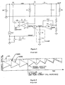
- Figure 1 shows a block diagram of a typical DC/DC converter using a peak-current control scheme.
- the converter includes a feedback arrangement including an error amplifier U3 that provides an error signal VERR1 as a function of the difference between the output voltage VOUT and a reference voltage VREF.
- the VERR1 signal is applied to the summer ⁇ .
- Summer ⁇ generates an error signal VERR2 representative of the difference between the VERR1 signal less a compensating ramp signal VRAMP.
- VERR2 is compared to a voltage representing the current flowing through inductor L 1 sensed by current sensor T1.
- the output of comparator U1 provides an input to the reset (R) input of a latch U2.
- the latch U2 receives a clocking input VCK at the set input (S).
- the Q output of the latch controls the opening and closing of the switch S1.
- the compensating ramp VRAMP is generated using a clocking signal VCK to open and close a switch which in turn is connected in parallel with a capacitor that receives current from a current source.
- VRAMP is subtracted from the error signal VERR1 so as to aid in stabilizing the current loop formed by comparator U1, latch U2, power switch S1 and current sensor T1.
- a clamp formed by diode D2 and voltage source VCL clamps the value of VERR1 to a maximum limited value.
- Operation is as follows. At the rising edge of the clock signal VCK, latch U2 is set and switch S1 turns on. The input voltage VIN is applied to the inductor L1, and the current ramps upward. When the current sensed by T1 reaches a value equal to the error signal VERR2, the latch is reset and the switch S1 is turned off. In normal operation, the error amp U3 adjusts the value of the error signal VERR1 in order to maintain a constant output voltage. During current limit operation, however, the error signal increases until it is limited to a maximum value set by the clamp formed from diode D2 and source VCL.
- the compensating ramp VRAMP is subtracted from the clamped error signal VERR1 to create the compensated error signal VERR2, the value of VERR2 at the moment that switch S1 is turned off will vary with the ON-time (Duty Cycle) of switch S1.
- the peak current during current limit will vary with output voltage, increasing as the output voltage decreases. If the amplitude of the compensating ramp is approximately equal to the clamp voltage set by VCL, then the peak current during current limit operation can vary by as much as 2:1 as the output voltage varies. This variation in the peak current is illustrated in Figure 2 .
- a second obstacle to obtaining a constant average current during current limit is the variation in ripple current that naturally occurs with changes in Vin and Vout.
- the ripple current is given approximately by: V IN - V OUT * t ON / L , wherein L is the value of the inductor, and t ON is the ON-time of the switch S1.
- a third obstacle to achieving a constant average current during current limit is the minimum controllable ON-time of switch S1.
- this is represented by the pulse width of VCK. Since latch U2 is set dominant, switch S1 will always be on for at least this minimum on- time, T ON,LIM .
- T ON,LIM the ON-time will decrease until it reaches this limiting value T ON,LIM . At this point, since the ON-time cannot be reduced any further, the average voltage delivered to the load becomes fixed, and the output current will increase significantly as the load resistance is further decreased.
- Figure 4 shows a typical voltage versus current characteristic for the DC/DC converter of Figure 1 .
- the initial tail-out of the average output current (the part of the curve between A and B) is caused by the variation in peak current due to slope compensation and the peak to average error.
- the sharp tail-out at lower output voltage (commencing at B) is caused by the minimum ON-time constraint.
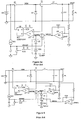
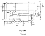
- Fig. 5b A second approach that overcomes this issue of instability during current limit is illustrated in Fig. 5b .
- the value of the clamp on VERR1 is adjusted dynamically based on the duty cycle so as to cancel the effect of slope compensation on peak current limit.
- a voltage VADJ is generated that corresponds to the instantaneous value of the compensating ramp at the time that switch S1 turns off. This voltage is then added to the VCL1 voltage to create the clamp voltage VCL2.
- a DC/DC converter is configured to provide a regulated output voltage and an current limited output current to a load.
- the converter comprises:
- a method of providing a limited output current at a regulated voltage to a load comprises:
- a DC/DC converter is configured to provide a regulated output voltage and a limited output current to a load.
- the converter comprises:
- a method of providing a limited output current at a regulated voltage to a load comprises:
- a DC/DC converter configured to provide a regulated output voltage and a limited output current to a load, the converter comprising:
- a method of providing a current limited output current at a regulated voltage to a load comprises:
- a DC/DC converter configured to provide a regulated output voltage and a limited output current to a load.
- the converter comprises:
- a method of providing a limited output current at a regulated voltage to a load comprises:
- Figure 1 is a partial schematic, partial block diagram illustrating a prior art DC/DC converter that presents one obstacle to achieving a constant average output current characteristic during current limit due to the variation in the peak current limit with duty cycle due to the compensating ramp generated in the converter;
- Figure 2 is a timing diagram further illustrating the problem provided by the prior art configuration shown in Figure 1 ;
- Figure 3 is a graphical illustration of how the average output current changes during current limit as a result of the peak to average current error in the configuration of Figure 1 ;
- Figure 4 shows a graphical illustration of a typical voltage versus current characteristic for the DC/DC converter of Figure 1 ;
- Figure 5a is a partial schematic, partial block diagram illustrating a prior art DC/DC converter
- Figure 5b is a partial schematic, partial block diagram illustrating another prior art DC/DC converter
- Figure 6 is a partial schematic, partial block diagram illustrating another prior art DC/DC converter
- Figure 7 is a partial schematic, partial block diagram of one embodiment of a DC/DC converter incorporating the teachings described herein;
- Figure 8 is a graphical illustration of the response of the Figure 7 embodiment, when the device goes into current limit
- Figure 9 is a partial schematic, partial block diagram of a second embodiment of a DC/DC converter incorporating the teachings described herein;
- Figure 10 is a graphical illustration of the response of the Figure 9 embodiment, when the device goes into current limit
- Figure 11 is a partial schematic, partial block diagram of a third embodiment of a DC/DC converter incorporating the teachings described herein;
- Figure 12 is a partial schematic, partial block diagram of a fourth embodiment of a DC/DC converter incorporating all three improvements described in connection with Figures 7-11 ;
- Figure 13 is a graphical illustration showing an output voltage versus output current characteristic of the Figure 12 embodiment.
- the variation in peak current with duty cycle during current limit is eliminated by varying the DC bias of the compensating ramp so that it is always equal to zero at the end of the ON-time of switch S1.
- an input voltage source VIN is connected between one side of switch S1 and system ground.
- the other side of switch S1 is coupled to the cathode of diode D1, and to one end of inductor L1.
- the other end of inductor L1 is connected to one plate of capacitor C1 and to the load RL.
- the anode of diode D1 and the opposite ends of the capacitor C1 and the load RL are connected to system ground.
- a feedback path is provided, with the node formed by connecting the inductor L1, capacitor C1 and the load RL together being connected to the resistor R1 of the voltage divider formed by resistors R1 and R2.
- the junction of the resistors R1 and R2 is connected to the inverting input of the error amplifier U3.
- the non-inverting input of the error amplifier U3 is connected to a reference voltage VREF so that the output of the error amplifier, VERR1, is an error signal as a function of the difference between the output voltage VOUT and the reference voltage VREF.
- the output of the error amplifier U3 is clamped with the clamp circuit formed by diode D2 and voltage source VCL connected between the output of the error amplifier U3 and system ground.
- the output of the error amplifier U3 is also connected to feedback capacitor CC, which in turn is connected to the inverting input of the amplifier U3 to form a feedback loop for the amplifier U3.
- the output of the amplifier U3 is also connected to the signal summer ⁇ 1, which in turn provides the error signal VERR2 as a function of the error signal VERR1 less the signal VR2 (described hereinafter).
- the error signal VERR2 is applied to the inverting input of a comparator U1.
- the non-inverting input of the comparator is connected to a signal sensor T1, positioned to sense the current through the inductor L1. This sensed current is converted to a voltage by a resistor (not shown).
- the output of the comparator which provides a signal as a function of the difference between VERR2 and the current sensed by sensor T1, is connected to the R input of the latch U2.
- the S input of latch U2 is connected so as to receive a clock signal VCK.
- the Q output of the latch U2 is a pulse width modulated (PWM) signal, which is used to control the opening and closing of the switch S1.
- PWM pulse width modulated
- the PWM output signal of the latch U2 is also applied to one-shot G1.
- the output of the latter is used to control the opening and closing of the switch S2 and provide an input to one-shot G2.
- One-shot G2 provides an output that controls the opening and closing of switch S3.
- a current source IDC is connected in series with the capacitor C4, which in turn is connected to system ground.
- the current source and capacitor C4 are connected in parallel with the input voltage source VIN.
- a switch S4 is connected in parallel with capacitor C4, both being connected between system ground and the node N1 formed between current source IDC and the capacitor C4 and the switch S2.
- a slope compensation signal VRAMP is provided at node N1 with the operation of switch S4 with the same clocking signal VCK applied to the S input to the latch U2.
- Node N1 is connected to the switch S2, which in turn is connected to switch S3.
- Switch S3 is connected to provide the VADJ signal to a minus input of the summer ⁇ 2.
- Capacitor C2 is provided between system ground and the junction formed between switches S2 and S3, and capacitor C3 is provided between system ground and the junction of switch C3 and summer ⁇ 2.
- the node N1 (the VRAMP signal) is also connected directly to the positive input of summer ⁇ 2.
- the output of summer ⁇ 2 is VR2 which equals VRAMP minus VADJ.
- VR2 is applied to a minus input of summer ⁇ 1, so that the output of summer ⁇ 1, VERR2, is equal to VERR1 minus VR2.
- FIG. 7 operates as follows, at the end of the switch ON-time (at the trailing edge of each pulse of the signal PWM), one-shot G1 is triggered generating a narrow, positive pulse on its output. This pulse momentarily closes switch S2, so that the VRAMP voltage at this instant is applied to capacitor C2. At the trailing edge of the pulse generated by one-shot G1, switch S2 is opened and a second pulse is generated by one-shot G2. This pulse in turn momentarily closes switch S3, shorting together capacitors C2 and C3. As a result, the cycle-by-cycle value of the slope compensation waveform VRAMP at the moment that switch S1 turns off is sampled and held on capacitor C2.
- This voltage is then low-pass filtered by capacitor C3, and then subtracted from the original VRAMP waveform.
- FIG. 7 Another unique advantage of the embodiment described in connection with Figure 7 is that the circuit is always actively adjusting the DC bias of the compensating ramp, even during normal operation. As a result, it is essentially a new variant on the peak current control architecture itself. In practice, the behavior of a current loop utilizing this approach is not dramatically different from conventional peak current control with slope compensation.
- Figure 8 illustrates the operation of Figure 7 embodiment as this circuit is driven into current limit. Note that as the output voltage collapses (to the right of the dashed vertical line), the voltage VADJ decreases as needed to make the peak sensed inductor current equal to the VCL voltage.
- an arrangement for addressing the problem of variation in ripple current that naturally occurs with changes in VIN and VOUT. While the arrangement described in connection with the embodiment illustrated in Figure 7 will make the peak current independent of duty cycle during current limit, the average output current can still vary considerably (15% or more) due to the variation in inductor (L1) ripple current with VIN, VOUT and Fsw. This problem is addressed in accordance with the teachings provided herein by adjusting the peak current limit clamp voltage VCL based on the instantaneous values of VIN, VOUT and Fsw in order to account for the given amount of inductor ripple current.
- Figure 9 One embodiment to adjusting the peak current limit clamp voltage VCL based on the these three values is shown in Figure 9 .
- the embodiment of Figure 9 is shown without the compensating ramp circuit in order to simplify the explanation of the circuit.
- the junction of the input voltage source VIN and the switch S1 is connected to a voltage-controlled current source B 1 having a transconductance g m defined by 1/R IPK .
- the output of the voltage-controlled current source is connected to the switch S3, switch S5 and capacitor C2.
- Switch S5 and capacitor C2 are each in turn connected to system ground, in parallel with one another.
- the output of switch S3, providing a voltage output VADJ is connected to capacitor C3 and a plus input to summer ⁇ 3 of the voltage clamp, the summer being connected between the diode D2 and the voltage source VCL so that VADJ adjusts the clamp voltage.
- Capacitor C3 and the voltage clamp are each connected to system ground.
- the clamp is used to clamp voltage VERR1, the output of the error amplifier U3.
- the output of error amplifier EA is connected to the inverting input of the comparator U1, which in turn provides an input to the R input of the latch U2.
- the pulse width modulated signal PWM output of the latter is used to operate switch S1, and is also provided to the NOR gate G1 and one-shot G2.
- the output of one-shot G2 is connected to a second input of NOR gate G1 and is also used to operate switch S3.
- the voltage-controlled current source B 1 generates a current of V IN - V OUT * R IPK .
- R IPK 2 ⁇ L / R S ⁇ C 2 where Rs is the effective resistance of current sensor T1
- the average output current in current limit will be independent of inductor current ripple.
- the amount of filtering needed from C3 is very slight.
- Figure 10 illustrates an exemplary operation of the Figure 9 embodiment, as the circuit is driven into current limit. Note that as the output voltage collapses, the VADJ voltage causes VERR1 to decrease so as to keep the average sensed inductor current approximately equal to the VCL voltage.
- the average current limit entry point will be independent of VIN and Fsw, and the average output current will remain constant as the output voltage falls. If the ON-time of switch S1 drops to the minimum achievable level T ON, MIN , then the output current becomes difficult to control and 1:1 dependent on switching frequency Fsw, the third obstacle to achieving a constant average current during current limit. To prevent this, a third improvement can be used to reduce the switching frequency Fsw by the optimum amount to keep the ON-time at an approximately constant value T ON, MIN that is somewhat greater than the hard-stop minimum ON-time T ON, MIN .
- This equation can be readily implemented by sensing VIN and VOUT and using an analog divider to achieve the needed fold-back characteristic that keeps the ON-time relatively constant and above the hard stop limit.
- a feed forward loop is provided and includes a current source I FMIN connected to the node between the input voltage source VIN and the switch S1.
- the source IFMIN is connected to a positive input of the summer ⁇ 4, which also receives VOUT at another positive input.
- the C output of the divider is connected to the input of the voltage controlled oscillator U4.
- the output of voltage controlled oscillator VCK forms the clocking input to the latch U2.
- the resistor R FMIN is used to establish a minimum fold-back frequency limit.
- Figure 12 illustrates an embodiment of a circuit arrangement that combines all three improvements in order to obtain an average current limit that is both fast and accurate. Using the circuit of Figure 12 , an output voltage versus output current characteristic as shown in Figure 13 (a "brick wall" response) can be readily obtained.
- embodiments of the present disclosure can have fewer, additional, and/or different components, steps, features, benefits and advantages than as expressly described herein. These also include embodiments in which the components and/or steps are arranged and/or ordered differently.
Landscapes
- Engineering & Computer Science (AREA)
- Power Engineering (AREA)
- Dc-Dc Converters (AREA)
Applications Claiming Priority (2)
| Application Number | Priority Date | Filing Date | Title |
|---|---|---|---|
| US24322809P | 2009-09-17 | 2009-09-17 | |
| EP10009840.9A EP2299578B1 (de) | 2009-09-17 | 2010-09-17 | Gleichspannungswandler mit einer schnellen und präzisen Begrenzung des Durchschnitts-Stroms |
Related Parent Applications (2)
| Application Number | Title | Priority Date | Filing Date |
|---|---|---|---|
| EP10009840.9 Division | 2010-09-17 | ||
| EP10009840.9A Division EP2299578B1 (de) | 2009-09-17 | 2010-09-17 | Gleichspannungswandler mit einer schnellen und präzisen Begrenzung des Durchschnitts-Stroms |
Publications (3)
| Publication Number | Publication Date |
|---|---|
| EP2323246A2 true EP2323246A2 (de) | 2011-05-18 |
| EP2323246A3 EP2323246A3 (de) | 2011-06-01 |
| EP2323246B1 EP2323246B1 (de) | 2014-12-24 |
Family
ID=43086720
Family Applications (3)
| Application Number | Title | Priority Date | Filing Date |
|---|---|---|---|
| EP11000952.9A Active EP2323246B1 (de) | 2009-09-17 | 2010-09-17 | Gleichspannungswandler mit einer schnellen und präzisen Begrenzung des Durchschnitts-Stroms |
| EP10009840.9A Active EP2299578B1 (de) | 2009-09-17 | 2010-09-17 | Gleichspannungswandler mit einer schnellen und präzisen Begrenzung des Durchschnitts-Stroms |
| EP11000951.1A Active EP2317634B1 (de) | 2009-09-17 | 2010-09-17 | Gleichspannungswandler mit einer schnellen und präzisen Begrenzung des Durchschnitts-Stroms |
Family Applications After (2)
| Application Number | Title | Priority Date | Filing Date |
|---|---|---|---|
| EP10009840.9A Active EP2299578B1 (de) | 2009-09-17 | 2010-09-17 | Gleichspannungswandler mit einer schnellen und präzisen Begrenzung des Durchschnitts-Stroms |
| EP11000951.1A Active EP2317634B1 (de) | 2009-09-17 | 2010-09-17 | Gleichspannungswandler mit einer schnellen und präzisen Begrenzung des Durchschnitts-Stroms |
Country Status (2)
| Country | Link |
|---|---|
| US (1) | US8421432B2 (de) |
| EP (3) | EP2323246B1 (de) |
Cited By (3)
| Publication number | Priority date | Publication date | Assignee | Title |
|---|---|---|---|---|
| US8975826B1 (en) | 2013-11-19 | 2015-03-10 | Terralux, Inc. | Output regulation with dynamic digital control loop compensation |
| US9209689B2 (en) | 2013-11-19 | 2015-12-08 | Terralux, Inc. | Output regulation with nonlinear digital control loop compensation |
| US9712046B2 (en) | 2011-09-12 | 2017-07-18 | Infineon Technologies Ag | Dead-time optimization of DC-DC converters |
Families Citing this family (57)
| Publication number | Priority date | Publication date | Assignee | Title |
|---|---|---|---|---|
| US20110140678A1 (en) * | 2009-12-14 | 2011-06-16 | Yee Philip W | Current limit recovery circuit |
| CN101917120B (zh) * | 2010-07-22 | 2012-10-03 | 魏其萃 | 用于开关电源的高精度峰值电感电流的控制装置 |
| CN102377342B (zh) * | 2011-08-12 | 2015-08-26 | 成都芯源系统有限公司 | 直流到直流变换电路的控制电路和控制方法 |
| ITTO20110893A1 (it) * | 2011-10-06 | 2013-04-07 | Alenia Aeronautica Spa | Sistema e metodo di gestione automatica dell'alimentazione elettrica per applicazioni aeronautiche |
| US9698679B2 (en) | 2011-11-07 | 2017-07-04 | Ams Ag | Circuit for DC-DC conversion with current limitation |
| US9024610B2 (en) * | 2012-05-01 | 2015-05-05 | Intersil Americas LLC | System and method of balanced slope compensation for switch mode regulators |
| US20140084884A1 (en) * | 2012-07-06 | 2014-03-27 | Jong J. Lee | Lc switching regulators |
| JP5482840B2 (ja) * | 2012-07-23 | 2014-05-07 | ダイキン工業株式会社 | 電源装置 |
| US8878509B2 (en) | 2012-08-17 | 2014-11-04 | St-Ericsson Sa | Current-mode controller for step-down (buck) converter |
| US9270171B2 (en) * | 2012-08-22 | 2016-02-23 | Allegro Microsystems, Llc | Methods and apparatus for DC-DC converter having dithered slope compensation |
| US9024600B2 (en) * | 2012-10-10 | 2015-05-05 | Texas Instruments Incorporated | PWM control apparatus for average output current balancing in multi-stage DC-DC converters |
| TWI470918B (zh) * | 2012-12-17 | 2015-01-21 | Upi Semiconductor Corp | 直流對直流轉換器、時間產生電路及其操作方法 |
| CN103280973B (zh) * | 2013-06-27 | 2015-07-29 | 电子科技大学 | 一种电流模式控制的开关电源 |
| CN103312200B (zh) * | 2013-06-28 | 2016-08-10 | 成都芯源系统有限公司 | 功率变换器、限流单元、控制电路及相关控制方法 |
| KR102116148B1 (ko) * | 2014-04-15 | 2020-06-08 | 매그나칩 반도체 유한회사 | 스위치 제어 회로 및 이를 이용한 변환기 |
| KR102169381B1 (ko) | 2014-04-17 | 2020-10-23 | 삼성전자주식회사 | Dc-dc 컨버터 및 이를 포함하는 전자 시스템 |
| KR101637650B1 (ko) * | 2014-05-20 | 2016-07-20 | 엘지이노텍 주식회사 | 직류-직류 변환기 |
| CN104201883B (zh) * | 2014-07-02 | 2017-02-15 | 成都芯源系统有限公司 | 一种用于开关转换器的控制电路 |
| US9431900B2 (en) | 2015-02-03 | 2016-08-30 | Astec International Limited | Dynamic operating frequency control of a buck power converter having a variable voltage output |
| US9450478B1 (en) * | 2015-04-10 | 2016-09-20 | Power Integrations, Inc. | Load responsive jitter |
| US9780662B1 (en) * | 2015-05-15 | 2017-10-03 | Maxim Integrated Products, Inc. | Method for portable sensor-less DC-DC converter control loops |
| ITUB20151055A1 (it) * | 2015-05-27 | 2016-11-27 | St Microelectronics Srl | Dispositivo e metodo di controllo di un convertitore di tensione e relativo convertitore di tensione |
| US9698691B2 (en) * | 2015-06-04 | 2017-07-04 | Dialog Semiconductor (Uk) Limited | Circuit and method for maximum duty cycle limitation in switching converters |
| WO2017001190A1 (en) * | 2015-06-29 | 2017-01-05 | Koninklijke Philips N.V. | Estimating an average value of an inductor current for switched-mode power converters |
| US10700600B2 (en) * | 2016-03-29 | 2020-06-30 | Intel Corporation | Duty cycle range control for envelope tracking switching regulators |
| US10630175B2 (en) * | 2016-08-03 | 2020-04-21 | Texas Instruments Incorporated | Pseudo current tracking for power supply regulation |
| US10491116B2 (en) | 2017-02-09 | 2019-11-26 | Microchip Technology Incorporated | Fast transient response circuit |
| US9941795B1 (en) | 2017-04-19 | 2018-04-10 | Dialog Semiconductor (Uk) Limited | Circuits and method for extracting average load current in DC-DC switching converters |
| US10581241B2 (en) * | 2017-06-22 | 2020-03-03 | Silicon Laboratories Inc. | Clamping inductive flyback voltage to reduce power dissipation |
| US10566904B2 (en) * | 2017-10-16 | 2020-02-18 | Texas Instruments Incorporated | Multimode PWM converter with smooth mode transition |
| EP3480933B1 (de) * | 2017-11-01 | 2021-03-03 | Goodix Technology (HK) Company Limited | Schaltung für ein schaltnetzteil |
| US11031867B2 (en) * | 2017-12-08 | 2021-06-08 | Cirrus Logic, Inc. | Digital-to-analog converter with embedded minimal error adaptive slope compensation for digital peak current controlled switched mode power supply |
| CN109002077B (zh) * | 2018-08-17 | 2020-07-10 | 电子科技大学 | 一种瞬态增强电路 |
| US10811952B2 (en) | 2018-09-05 | 2020-10-20 | Cypress Semiconductor Corporation | Systems, methods, and devices for fast wakeup of DC-DC converters including feedback regulation loops |
| US10587196B1 (en) * | 2019-02-22 | 2020-03-10 | Elite Semiconductor Memory Technology Inc. | Constant on-time controller and buck regulator device using the same |
| CN112019045B (zh) * | 2019-05-29 | 2021-09-21 | 晶豪科技股份有限公司 | 固定开路时间控制器与使用其的降压变换器器件 |
| CN110581639B (zh) * | 2019-09-04 | 2020-09-15 | 广州金升阳科技有限公司 | 电流型降压转换器轻重载模式切换快速响应方法和电路 |
| US10833661B1 (en) * | 2019-12-04 | 2020-11-10 | Alpha And Omega Semiconductor (Cayman) Ltd. | Slope compensation for peak current mode control modulator |
| US11424672B2 (en) * | 2020-01-27 | 2022-08-23 | Qualcomm Incorporated | Current limiting for a boost converter |
| CN111431405B (zh) * | 2020-04-13 | 2021-05-14 | 矽力杰半导体技术(杭州)有限公司 | 电压纹波控制电路及控制方法 |
| US11973424B2 (en) | 2020-09-08 | 2024-04-30 | Analog Devices International Unlimited Company | Spur free switching regulator with self-adaptive cancellation of coil current ripple |
| US11742741B2 (en) | 2020-09-08 | 2023-08-29 | Analog Devices International Unlimited Company | Spurious noise reduction by monotonic frequency stepping with compensation of error amplifier's output in peak current mode switching regulator |
| CN112072938B (zh) * | 2020-09-14 | 2022-03-08 | 昂宝电子(上海)有限公司 | 用于改善开关电源的输出电压负载调整率的装置和方法 |
| CN112953224B (zh) * | 2021-03-26 | 2022-07-22 | 广州视琨电子科技有限公司 | Dc-dc转换电路及电源 |
| US12095366B2 (en) | 2021-04-06 | 2024-09-17 | Semiconductor Components Industries, Llc | Current limiting circuit |
| US12431796B2 (en) * | 2021-07-09 | 2025-09-30 | Reed Semiconductor Corporation | Frequency lock loop for constant switching frequency of DC-DC converters |
| CN113922668B (zh) * | 2021-09-07 | 2024-01-16 | 西安理工大学 | 应用于dc-dc转换器的单粒子瞬态加固电路及方法 |
| CN113872430B (zh) * | 2021-09-13 | 2023-07-18 | 珠海格力电器股份有限公司 | 功率因素校正电路及其电流过零畸变抑制方法、空调器 |
| US12003178B2 (en) | 2021-11-12 | 2024-06-04 | Diodes Incorporated | Adaptive minimum duty cycle design to extend operational voltage range for DCDC converters |
| CN114710035B (zh) * | 2021-11-26 | 2025-10-24 | 杰华特微电子股份有限公司 | 一种开关电路的控制方法、控制电路及开关电路 |
| CN114553004B (zh) * | 2022-02-16 | 2026-01-06 | 深圳威迈斯新能源(集团)股份有限公司 | 一种逆变电路直流电压低频纹波补偿电路及其控制方法 |
| CN114977793B (zh) * | 2022-06-21 | 2026-01-23 | 骏盈半导体(上海)有限公司 | 用于基于acot控制模式的dc-dc变换器的自适应斜坡补偿电路 |
| KR20240044559A (ko) * | 2022-09-28 | 2024-04-05 | 삼성디스플레이 주식회사 | 전원 전압 생성부 및 이를 포함하는 표시 장치 |
| US20240405663A1 (en) * | 2023-05-30 | 2024-12-05 | Texas Instruments Incorporated | Power converter compensation for ground bouncing |
| US12334811B2 (en) * | 2023-06-14 | 2025-06-17 | Stmicroelectronics International N.V. | Closed loop stability ramp implementation for Constant On-Time buck converter |
| US12537437B2 (en) * | 2023-08-23 | 2026-01-27 | Renesas Electronics Corporation | Single control signal generation in power stage controller |
| CN120185360B (zh) * | 2025-03-11 | 2025-09-30 | 晟芯腾跃(北京)科技有限公司 | 一种电压模dcdc变换器的负载瞬态增强电路 |
Family Cites Families (9)
| Publication number | Priority date | Publication date | Assignee | Title |
|---|---|---|---|---|
| JPS63305754A (ja) | 1987-06-03 | 1988-12-13 | Kokusai Electric Co Ltd | スイッチングレギュレ−タ回路 |
| US5717322A (en) | 1996-02-16 | 1998-02-10 | Harris Corporation | Method to improve the peak-current limit in a slope-compensated, current-mode DC/DC converter, and circuit therefor |
| JP3467679B2 (ja) | 1998-05-11 | 2003-11-17 | 株式会社豊田自動織機 | Dc/dc変換器 |
| US6498466B1 (en) | 2000-05-23 | 2002-12-24 | Linear Technology Corp. | Cancellation of slope compensation effect on current limit |
| US7145317B1 (en) | 2004-12-13 | 2006-12-05 | Intersil Americas Inc. | Constant frequency duty cycle independent synthetic ripple regulator |
| US7615978B2 (en) | 2005-07-22 | 2009-11-10 | Fairchild Semiconductor Corporation | Current mode control with feed-forward for power devices |
| US7733671B2 (en) | 2006-06-23 | 2010-06-08 | Mediatek Inc. | Switching regulators |
| US8213193B2 (en) * | 2006-12-01 | 2012-07-03 | O2Micro Inc | Flyback DC-DC converter with feedback control |
| US8169205B2 (en) * | 2009-05-26 | 2012-05-01 | Silergy Technology | Control for regulator fast transient response and low EMI noise |
-
2010
- 2010-09-16 US US12/884,013 patent/US8421432B2/en active Active
- 2010-09-17 EP EP11000952.9A patent/EP2323246B1/de active Active
- 2010-09-17 EP EP10009840.9A patent/EP2299578B1/de active Active
- 2010-09-17 EP EP11000951.1A patent/EP2317634B1/de active Active
Non-Patent Citations (1)
| Title |
|---|
| None |
Cited By (3)
| Publication number | Priority date | Publication date | Assignee | Title |
|---|---|---|---|---|
| US9712046B2 (en) | 2011-09-12 | 2017-07-18 | Infineon Technologies Ag | Dead-time optimization of DC-DC converters |
| US8975826B1 (en) | 2013-11-19 | 2015-03-10 | Terralux, Inc. | Output regulation with dynamic digital control loop compensation |
| US9209689B2 (en) | 2013-11-19 | 2015-12-08 | Terralux, Inc. | Output regulation with nonlinear digital control loop compensation |
Also Published As
| Publication number | Publication date |
|---|---|
| EP2299578B1 (de) | 2013-07-31 |
| EP2317634A3 (de) | 2011-05-25 |
| EP2299578A2 (de) | 2011-03-23 |
| EP2317634A2 (de) | 2011-05-04 |
| EP2299578A3 (de) | 2011-05-04 |
| EP2323246B1 (de) | 2014-12-24 |
| US20110062932A1 (en) | 2011-03-17 |
| EP2317634B1 (de) | 2017-06-21 |
| EP2323246A3 (de) | 2011-06-01 |
| US8421432B2 (en) | 2013-04-16 |
Similar Documents
| Publication | Publication Date | Title |
|---|---|---|
| EP2317634B1 (de) | Gleichspannungswandler mit einer schnellen und präzisen Begrenzung des Durchschnitts-Stroms | |
| US8487593B2 (en) | System and method for detection and compensation of aggressive output filters for switched mode power supplies | |
| CN102332826B (zh) | 用于反激式电源变换器的初级侧感测和调整的系统和方法 | |
| US11381167B2 (en) | Power converter with slope compensation | |
| US8085005B2 (en) | Buck-boost converter with sample and hold circuit in current loop | |
| US9621041B2 (en) | Buck-boost converter control circuits and techniques | |
| US7109692B1 (en) | High-speed PWM control apparatus for power converters with adaptive voltage position and its driving signal generating method | |
| TWI612847B (zh) | 用於產生輸出電壓至發光二極體串之方法及電路 | |
| JP4725641B2 (ja) | 昇降圧型スイッチングレギュレータ | |
| US20140125306A1 (en) | Switching Regulator Control with Nonlinear Feed-Forward Correction | |
| US8232782B2 (en) | System and method for equalizing the small signal response of variable phase voltage regulators | |
| EP1655825A2 (de) | Spannungsoffsetabgleich für eine integrierte Verstärkerschaltung | |
| US9030183B2 (en) | Soft-start control techniques for a switched-mode power supply | |
| US20080030183A1 (en) | Method of feedback controlling a switched regulator | |
| EP1187303B1 (de) | Pulsbreitenmodulationsteuerschaltung für Gleichstrom-Gleichstromwandler | |
| US11616442B2 (en) | Inductor current dependent pulse width modulator in a SIMO converter | |
| US6972974B2 (en) | Compensator to achieve constant bandwidth in a switching regulator | |
| US7688050B2 (en) | Switching power supply controller with unidirectional transient gain change | |
| EP3525332B1 (de) | Laststromaufschaltungsschemata für strommodusgesteuerte leistungswandler | |
| US8222878B2 (en) | Current mode DC-DC converter having a pulse width modulation signal of reduced delay | |
| US12587082B2 (en) | Dynamic AC droop control for DC-DC regulators | |
| US8344703B2 (en) | Variable on-time control method for high light-load efficiency, small output voltage ripple, and audible-noise-free operation | |
| TWI406486B (zh) | 用於反激式電源變換器的初級側感測和調整的系統和方法 | |
| CN110971126B (zh) | 开关电源及其控制装置和环路补偿方法及存储介质 | |
| KR101043580B1 (ko) | 직류/직류 변환기 |
Legal Events
| Date | Code | Title | Description |
|---|---|---|---|
| PUAI | Public reference made under article 153(3) epc to a published international application that has entered the european phase |
Free format text: ORIGINAL CODE: 0009012 |
|
| PUAL | Search report despatched |
Free format text: ORIGINAL CODE: 0009013 |
|
| AC | Divisional application: reference to earlier application |
Ref document number: 2299578 Country of ref document: EP Kind code of ref document: P |
|
| AK | Designated contracting states |
Kind code of ref document: A2 Designated state(s): AL AT BE BG CH CY CZ DE DK EE ES FI FR GB GR HR HU IE IS IT LI LT LU LV MC MK MT NL NO PL PT RO SE SI SK SM TR |
|
| AX | Request for extension of the european patent |
Extension state: BA ME RS |
|
| AK | Designated contracting states |
Kind code of ref document: A3 Designated state(s): AL AT BE BG CH CY CZ DE DK EE ES FI FR GB GR HR HU IE IS IT LI LT LU LV MC MK MT NL NO PL PT RO SE SI SK SM TR |
|
| AX | Request for extension of the european patent |
Extension state: BA ME RS |
|
| RAP1 | Party data changed (applicant data changed or rights of an application transferred) |
Owner name: LINEAR TECHNOLOGY CORPORATION |
|
| 17P | Request for examination filed |
Effective date: 20111130 |
|
| 17Q | First examination report despatched |
Effective date: 20140403 |
|
| GRAJ | Information related to disapproval of communication of intention to grant by the applicant or resumption of examination proceedings by the epo deleted |
Free format text: ORIGINAL CODE: EPIDOSDIGR1 |
|
| GRAP | Despatch of communication of intention to grant a patent |
Free format text: ORIGINAL CODE: EPIDOSNIGR1 |
|
| GRAP | Despatch of communication of intention to grant a patent |
Free format text: ORIGINAL CODE: EPIDOSNIGR1 |
|
| INTG | Intention to grant announced |
Effective date: 20140929 |
|
| GRAS | Grant fee paid |
Free format text: ORIGINAL CODE: EPIDOSNIGR3 |
|
| GRAA | (expected) grant |
Free format text: ORIGINAL CODE: 0009210 |
|
| AC | Divisional application: reference to earlier application |
Ref document number: 2299578 Country of ref document: EP Kind code of ref document: P |
|
| AK | Designated contracting states |
Kind code of ref document: B1 Designated state(s): AL AT BE BG CH CY CZ DE DK EE ES FI FR GB GR HR HU IE IS IT LI LT LU LV MC MK MT NL NO PL PT RO SE SI SK SM TR |
|
| REG | Reference to a national code |
Ref country code: GB Ref legal event code: FG4D |
|
| REG | Reference to a national code |
Ref country code: CH Ref legal event code: EP |
|
| REG | Reference to a national code |
Ref country code: IE Ref legal event code: FG4D |
|
| REG | Reference to a national code |
Ref country code: AT Ref legal event code: REF Ref document number: 703571 Country of ref document: AT Kind code of ref document: T Effective date: 20150115 |
|
| REG | Reference to a national code |
Ref country code: NL Ref legal event code: T3 |
|
| REG | Reference to a national code |
Ref country code: DE Ref legal event code: R096 Ref document number: 602010021326 Country of ref document: DE Effective date: 20150219 |
|
| PG25 | Lapsed in a contracting state [announced via postgrant information from national office to epo] |
Ref country code: FI Free format text: LAPSE BECAUSE OF FAILURE TO SUBMIT A TRANSLATION OF THE DESCRIPTION OR TO PAY THE FEE WITHIN THE PRESCRIBED TIME-LIMIT Effective date: 20141224 Ref country code: LT Free format text: LAPSE BECAUSE OF FAILURE TO SUBMIT A TRANSLATION OF THE DESCRIPTION OR TO PAY THE FEE WITHIN THE PRESCRIBED TIME-LIMIT Effective date: 20141224 Ref country code: NO Free format text: LAPSE BECAUSE OF FAILURE TO SUBMIT A TRANSLATION OF THE DESCRIPTION OR TO PAY THE FEE WITHIN THE PRESCRIBED TIME-LIMIT Effective date: 20150324 |
|
| REG | Reference to a national code |
Ref country code: LT Ref legal event code: MG4D |
|
| PG25 | Lapsed in a contracting state [announced via postgrant information from national office to epo] |
Ref country code: HR Free format text: LAPSE BECAUSE OF FAILURE TO SUBMIT A TRANSLATION OF THE DESCRIPTION OR TO PAY THE FEE WITHIN THE PRESCRIBED TIME-LIMIT Effective date: 20141224 Ref country code: GR Free format text: LAPSE BECAUSE OF FAILURE TO SUBMIT A TRANSLATION OF THE DESCRIPTION OR TO PAY THE FEE WITHIN THE PRESCRIBED TIME-LIMIT Effective date: 20150325 Ref country code: LV Free format text: LAPSE BECAUSE OF FAILURE TO SUBMIT A TRANSLATION OF THE DESCRIPTION OR TO PAY THE FEE WITHIN THE PRESCRIBED TIME-LIMIT Effective date: 20141224 Ref country code: SE Free format text: LAPSE BECAUSE OF FAILURE TO SUBMIT A TRANSLATION OF THE DESCRIPTION OR TO PAY THE FEE WITHIN THE PRESCRIBED TIME-LIMIT Effective date: 20141224 |
|
| REG | Reference to a national code |
Ref country code: AT Ref legal event code: MK05 Ref document number: 703571 Country of ref document: AT Kind code of ref document: T Effective date: 20141224 |
|
| PG25 | Lapsed in a contracting state [announced via postgrant information from national office to epo] |
Ref country code: CZ Free format text: LAPSE BECAUSE OF FAILURE TO SUBMIT A TRANSLATION OF THE DESCRIPTION OR TO PAY THE FEE WITHIN THE PRESCRIBED TIME-LIMIT Effective date: 20141224 Ref country code: RO Free format text: LAPSE BECAUSE OF FAILURE TO SUBMIT A TRANSLATION OF THE DESCRIPTION OR TO PAY THE FEE WITHIN THE PRESCRIBED TIME-LIMIT Effective date: 20141224 Ref country code: EE Free format text: LAPSE BECAUSE OF FAILURE TO SUBMIT A TRANSLATION OF THE DESCRIPTION OR TO PAY THE FEE WITHIN THE PRESCRIBED TIME-LIMIT Effective date: 20141224 Ref country code: ES Free format text: LAPSE BECAUSE OF FAILURE TO SUBMIT A TRANSLATION OF THE DESCRIPTION OR TO PAY THE FEE WITHIN THE PRESCRIBED TIME-LIMIT Effective date: 20141224 Ref country code: SK Free format text: LAPSE BECAUSE OF FAILURE TO SUBMIT A TRANSLATION OF THE DESCRIPTION OR TO PAY THE FEE WITHIN THE PRESCRIBED TIME-LIMIT Effective date: 20141224 |
|
| PG25 | Lapsed in a contracting state [announced via postgrant information from national office to epo] |
Ref country code: AT Free format text: LAPSE BECAUSE OF FAILURE TO SUBMIT A TRANSLATION OF THE DESCRIPTION OR TO PAY THE FEE WITHIN THE PRESCRIBED TIME-LIMIT Effective date: 20141224 Ref country code: IS Free format text: LAPSE BECAUSE OF FAILURE TO SUBMIT A TRANSLATION OF THE DESCRIPTION OR TO PAY THE FEE WITHIN THE PRESCRIBED TIME-LIMIT Effective date: 20150424 Ref country code: PL Free format text: LAPSE BECAUSE OF FAILURE TO SUBMIT A TRANSLATION OF THE DESCRIPTION OR TO PAY THE FEE WITHIN THE PRESCRIBED TIME-LIMIT Effective date: 20141224 |
|
| REG | Reference to a national code |
Ref country code: DE Ref legal event code: R097 Ref document number: 602010021326 Country of ref document: DE |
|
| PG25 | Lapsed in a contracting state [announced via postgrant information from national office to epo] |
Ref country code: DK Free format text: LAPSE BECAUSE OF FAILURE TO SUBMIT A TRANSLATION OF THE DESCRIPTION OR TO PAY THE FEE WITHIN THE PRESCRIBED TIME-LIMIT Effective date: 20141224 |
|
| PLBE | No opposition filed within time limit |
Free format text: ORIGINAL CODE: 0009261 |
|
| STAA | Information on the status of an ep patent application or granted ep patent |
Free format text: STATUS: NO OPPOSITION FILED WITHIN TIME LIMIT |
|
| 26N | No opposition filed |
Effective date: 20150925 |
|
| PG25 | Lapsed in a contracting state [announced via postgrant information from national office to epo] |
Ref country code: SI Free format text: LAPSE BECAUSE OF FAILURE TO SUBMIT A TRANSLATION OF THE DESCRIPTION OR TO PAY THE FEE WITHIN THE PRESCRIBED TIME-LIMIT Effective date: 20141224 |
|
| PG25 | Lapsed in a contracting state [announced via postgrant information from national office to epo] |
Ref country code: LU Free format text: LAPSE BECAUSE OF FAILURE TO SUBMIT A TRANSLATION OF THE DESCRIPTION OR TO PAY THE FEE WITHIN THE PRESCRIBED TIME-LIMIT Effective date: 20150917 Ref country code: MC Free format text: LAPSE BECAUSE OF FAILURE TO SUBMIT A TRANSLATION OF THE DESCRIPTION OR TO PAY THE FEE WITHIN THE PRESCRIBED TIME-LIMIT Effective date: 20141224 |
|
| REG | Reference to a national code |
Ref country code: CH Ref legal event code: PL |
|
| PG25 | Lapsed in a contracting state [announced via postgrant information from national office to epo] |
Ref country code: BE Free format text: LAPSE BECAUSE OF FAILURE TO SUBMIT A TRANSLATION OF THE DESCRIPTION OR TO PAY THE FEE WITHIN THE PRESCRIBED TIME-LIMIT Effective date: 20141224 |
|
| REG | Reference to a national code |
Ref country code: IE Ref legal event code: MM4A |
|
| PG25 | Lapsed in a contracting state [announced via postgrant information from national office to epo] |
Ref country code: IE Free format text: LAPSE BECAUSE OF NON-PAYMENT OF DUE FEES Effective date: 20150917 Ref country code: CH Free format text: LAPSE BECAUSE OF NON-PAYMENT OF DUE FEES Effective date: 20150930 Ref country code: LI Free format text: LAPSE BECAUSE OF NON-PAYMENT OF DUE FEES Effective date: 20150930 |
|
| REG | Reference to a national code |
Ref country code: FR Ref legal event code: PLFP Year of fee payment: 7 |
|
| PG25 | Lapsed in a contracting state [announced via postgrant information from national office to epo] |
Ref country code: MT Free format text: LAPSE BECAUSE OF FAILURE TO SUBMIT A TRANSLATION OF THE DESCRIPTION OR TO PAY THE FEE WITHIN THE PRESCRIBED TIME-LIMIT Effective date: 20141224 |
|
| PG25 | Lapsed in a contracting state [announced via postgrant information from national office to epo] |
Ref country code: BG Free format text: LAPSE BECAUSE OF FAILURE TO SUBMIT A TRANSLATION OF THE DESCRIPTION OR TO PAY THE FEE WITHIN THE PRESCRIBED TIME-LIMIT Effective date: 20141224 Ref country code: SM Free format text: LAPSE BECAUSE OF FAILURE TO SUBMIT A TRANSLATION OF THE DESCRIPTION OR TO PAY THE FEE WITHIN THE PRESCRIBED TIME-LIMIT Effective date: 20141224 Ref country code: HU Free format text: LAPSE BECAUSE OF FAILURE TO SUBMIT A TRANSLATION OF THE DESCRIPTION OR TO PAY THE FEE WITHIN THE PRESCRIBED TIME-LIMIT; INVALID AB INITIO Effective date: 20100917 |
|
| PG25 | Lapsed in a contracting state [announced via postgrant information from national office to epo] |
Ref country code: CY Free format text: LAPSE BECAUSE OF FAILURE TO SUBMIT A TRANSLATION OF THE DESCRIPTION OR TO PAY THE FEE WITHIN THE PRESCRIBED TIME-LIMIT Effective date: 20141224 |
|
| PG25 | Lapsed in a contracting state [announced via postgrant information from national office to epo] |
Ref country code: TR Free format text: LAPSE BECAUSE OF FAILURE TO SUBMIT A TRANSLATION OF THE DESCRIPTION OR TO PAY THE FEE WITHIN THE PRESCRIBED TIME-LIMIT Effective date: 20141224 |
|
| REG | Reference to a national code |
Ref country code: FR Ref legal event code: PLFP Year of fee payment: 8 |
|
| PG25 | Lapsed in a contracting state [announced via postgrant information from national office to epo] |
Ref country code: MK Free format text: LAPSE BECAUSE OF FAILURE TO SUBMIT A TRANSLATION OF THE DESCRIPTION OR TO PAY THE FEE WITHIN THE PRESCRIBED TIME-LIMIT Effective date: 20141224 |
|
| PG25 | Lapsed in a contracting state [announced via postgrant information from national office to epo] |
Ref country code: PT Free format text: LAPSE BECAUSE OF FAILURE TO SUBMIT A TRANSLATION OF THE DESCRIPTION OR TO PAY THE FEE WITHIN THE PRESCRIBED TIME-LIMIT Effective date: 20141224 |
|
| REG | Reference to a national code |
Ref country code: FR Ref legal event code: PLFP Year of fee payment: 9 |
|
| PG25 | Lapsed in a contracting state [announced via postgrant information from national office to epo] |
Ref country code: AL Free format text: LAPSE BECAUSE OF FAILURE TO SUBMIT A TRANSLATION OF THE DESCRIPTION OR TO PAY THE FEE WITHIN THE PRESCRIBED TIME-LIMIT Effective date: 20141224 |
|
| REG | Reference to a national code |
Ref country code: DE Ref legal event code: R082 Ref document number: 602010021326 Country of ref document: DE Representative=s name: WITHERS & ROGERS LLP, DE Ref country code: DE Ref legal event code: R082 Ref document number: 602010021326 Country of ref document: DE Representative=s name: MUELLER-BORE & PARTNER PATENTANWAELTE PARTG MB, DE Ref country code: DE Ref legal event code: R081 Ref document number: 602010021326 Country of ref document: DE Owner name: ANALOG DEVICES INTERNATIONAL UNLIMITED COMPANY, IE Free format text: FORMER OWNER: LINEAR TECHNOLOGY CORP., MILPITAS, CALIF., US |
|
| REG | Reference to a national code |
Ref country code: DE Ref legal event code: R082 Ref document number: 602010021326 Country of ref document: DE Representative=s name: WITHERS & ROGERS LLP, DE |
|
| PGFP | Annual fee paid to national office [announced via postgrant information from national office to epo] |
Ref country code: IT Payment date: 20210824 Year of fee payment: 12 |
|
| REG | Reference to a national code |
Ref country code: GB Ref legal event code: 732E Free format text: REGISTERED BETWEEN 20211125 AND 20211201 |
|
| REG | Reference to a national code |
Ref country code: NL Ref legal event code: PD Owner name: ANALOG DEVICES INTERNATIONAL UNLIMITED COMPANY; IE Free format text: DETAILS ASSIGNMENT: CHANGE OF OWNER(S), ASSIGNMENT; FORMER OWNER NAME: LINEAR TECHNOLOGY LLC Effective date: 20211216 |
|
| PG25 | Lapsed in a contracting state [announced via postgrant information from national office to epo] |
Ref country code: IT Free format text: LAPSE BECAUSE OF NON-PAYMENT OF DUE FEES Effective date: 20220917 |
|
| PGFP | Annual fee paid to national office [announced via postgrant information from national office to epo] |
Ref country code: NL Payment date: 20240820 Year of fee payment: 15 |
|
| PGFP | Annual fee paid to national office [announced via postgrant information from national office to epo] |
Ref country code: DE Payment date: 20240820 Year of fee payment: 15 |
|
| PGFP | Annual fee paid to national office [announced via postgrant information from national office to epo] |
Ref country code: GB Payment date: 20240820 Year of fee payment: 15 |
|
| PGFP | Annual fee paid to national office [announced via postgrant information from national office to epo] |
Ref country code: FR Payment date: 20240820 Year of fee payment: 15 |