EP2322980A2 - In-plane switching mode liquid crystal display - Google Patents
In-plane switching mode liquid crystal display Download PDFInfo
- Publication number
- EP2322980A2 EP2322980A2 EP09810178A EP09810178A EP2322980A2 EP 2322980 A2 EP2322980 A2 EP 2322980A2 EP 09810178 A EP09810178 A EP 09810178A EP 09810178 A EP09810178 A EP 09810178A EP 2322980 A2 EP2322980 A2 EP 2322980A2
- Authority
- EP
- European Patent Office
- Prior art keywords
- liquid crystal
- film
- crystal display
- acryl
- ips
- Prior art date
- Legal status (The legal status is an assumption and is not a legal conclusion. Google has not performed a legal analysis and makes no representation as to the accuracy of the status listed.)
- Granted
Links
Images
Classifications
-
- G—PHYSICS
- G02—OPTICS
- G02F—OPTICAL DEVICES OR ARRANGEMENTS FOR THE CONTROL OF LIGHT BY MODIFICATION OF THE OPTICAL PROPERTIES OF THE MEDIA OF THE ELEMENTS INVOLVED THEREIN; NON-LINEAR OPTICS; FREQUENCY-CHANGING OF LIGHT; OPTICAL LOGIC ELEMENTS; OPTICAL ANALOGUE/DIGITAL CONVERTERS
- G02F1/00—Devices or arrangements for the control of the intensity, colour, phase, polarisation or direction of light arriving from an independent light source, e.g. switching, gating or modulating; Non-linear optics
- G02F1/01—Devices or arrangements for the control of the intensity, colour, phase, polarisation or direction of light arriving from an independent light source, e.g. switching, gating or modulating; Non-linear optics for the control of the intensity, phase, polarisation or colour
- G02F1/13—Devices or arrangements for the control of the intensity, colour, phase, polarisation or direction of light arriving from an independent light source, e.g. switching, gating or modulating; Non-linear optics for the control of the intensity, phase, polarisation or colour based on liquid crystals, e.g. single liquid crystal display cells
- G02F1/133—Constructional arrangements; Operation of liquid crystal cells; Circuit arrangements
- G02F1/1333—Constructional arrangements; Manufacturing methods
- G02F1/1335—Structural association of cells with optical devices, e.g. polarisers or reflectors
- G02F1/13363—Birefringent elements, e.g. for optical compensation
- G02F1/133634—Birefringent elements, e.g. for optical compensation the refractive index Nz perpendicular to the element surface being different from in-plane refractive indices Nx and Ny, e.g. biaxial or with normal optical axis
-
- G—PHYSICS
- G02—OPTICS
- G02F—OPTICAL DEVICES OR ARRANGEMENTS FOR THE CONTROL OF LIGHT BY MODIFICATION OF THE OPTICAL PROPERTIES OF THE MEDIA OF THE ELEMENTS INVOLVED THEREIN; NON-LINEAR OPTICS; FREQUENCY-CHANGING OF LIGHT; OPTICAL LOGIC ELEMENTS; OPTICAL ANALOGUE/DIGITAL CONVERTERS
- G02F1/00—Devices or arrangements for the control of the intensity, colour, phase, polarisation or direction of light arriving from an independent light source, e.g. switching, gating or modulating; Non-linear optics
- G02F1/01—Devices or arrangements for the control of the intensity, colour, phase, polarisation or direction of light arriving from an independent light source, e.g. switching, gating or modulating; Non-linear optics for the control of the intensity, phase, polarisation or colour
- G02F1/13—Devices or arrangements for the control of the intensity, colour, phase, polarisation or direction of light arriving from an independent light source, e.g. switching, gating or modulating; Non-linear optics for the control of the intensity, phase, polarisation or colour based on liquid crystals, e.g. single liquid crystal display cells
- G02F1/133—Constructional arrangements; Operation of liquid crystal cells; Circuit arrangements
- G02F1/1333—Constructional arrangements; Manufacturing methods
- G02F1/1335—Structural association of cells with optical devices, e.g. polarisers or reflectors
-
- G—PHYSICS
- G02—OPTICS
- G02F—OPTICAL DEVICES OR ARRANGEMENTS FOR THE CONTROL OF LIGHT BY MODIFICATION OF THE OPTICAL PROPERTIES OF THE MEDIA OF THE ELEMENTS INVOLVED THEREIN; NON-LINEAR OPTICS; FREQUENCY-CHANGING OF LIGHT; OPTICAL LOGIC ELEMENTS; OPTICAL ANALOGUE/DIGITAL CONVERTERS
- G02F1/00—Devices or arrangements for the control of the intensity, colour, phase, polarisation or direction of light arriving from an independent light source, e.g. switching, gating or modulating; Non-linear optics
- G02F1/01—Devices or arrangements for the control of the intensity, colour, phase, polarisation or direction of light arriving from an independent light source, e.g. switching, gating or modulating; Non-linear optics for the control of the intensity, phase, polarisation or colour
- G02F1/13—Devices or arrangements for the control of the intensity, colour, phase, polarisation or direction of light arriving from an independent light source, e.g. switching, gating or modulating; Non-linear optics for the control of the intensity, phase, polarisation or colour based on liquid crystals, e.g. single liquid crystal display cells
- G02F1/133—Constructional arrangements; Operation of liquid crystal cells; Circuit arrangements
- G02F1/1333—Constructional arrangements; Manufacturing methods
- G02F1/1335—Structural association of cells with optical devices, e.g. polarisers or reflectors
- G02F1/13363—Birefringent elements, e.g. for optical compensation
-
- G—PHYSICS
- G02—OPTICS
- G02F—OPTICAL DEVICES OR ARRANGEMENTS FOR THE CONTROL OF LIGHT BY MODIFICATION OF THE OPTICAL PROPERTIES OF THE MEDIA OF THE ELEMENTS INVOLVED THEREIN; NON-LINEAR OPTICS; FREQUENCY-CHANGING OF LIGHT; OPTICAL LOGIC ELEMENTS; OPTICAL ANALOGUE/DIGITAL CONVERTERS
- G02F1/00—Devices or arrangements for the control of the intensity, colour, phase, polarisation or direction of light arriving from an independent light source, e.g. switching, gating or modulating; Non-linear optics
- G02F1/01—Devices or arrangements for the control of the intensity, colour, phase, polarisation or direction of light arriving from an independent light source, e.g. switching, gating or modulating; Non-linear optics for the control of the intensity, phase, polarisation or colour
- G02F1/13—Devices or arrangements for the control of the intensity, colour, phase, polarisation or direction of light arriving from an independent light source, e.g. switching, gating or modulating; Non-linear optics for the control of the intensity, phase, polarisation or colour based on liquid crystals, e.g. single liquid crystal display cells
- G02F1/133—Constructional arrangements; Operation of liquid crystal cells; Circuit arrangements
- G02F1/1333—Constructional arrangements; Manufacturing methods
- G02F1/1343—Electrodes
- G02F1/134309—Electrodes characterised by their geometrical arrangement
- G02F1/134363—Electrodes characterised by their geometrical arrangement for applying an electric field parallel to the substrate, i.e. in-plane switching [IPS]
-
- G—PHYSICS
- G02—OPTICS
- G02F—OPTICAL DEVICES OR ARRANGEMENTS FOR THE CONTROL OF LIGHT BY MODIFICATION OF THE OPTICAL PROPERTIES OF THE MEDIA OF THE ELEMENTS INVOLVED THEREIN; NON-LINEAR OPTICS; FREQUENCY-CHANGING OF LIGHT; OPTICAL LOGIC ELEMENTS; OPTICAL ANALOGUE/DIGITAL CONVERTERS
- G02F2413/00—Indexing scheme related to G02F1/13363, i.e. to birefringent elements, e.g. for optical compensation, characterised by the number, position, orientation or value of the compensation plates
- G02F2413/02—Number of plates being 2
-
- G—PHYSICS
- G02—OPTICS
- G02F—OPTICAL DEVICES OR ARRANGEMENTS FOR THE CONTROL OF LIGHT BY MODIFICATION OF THE OPTICAL PROPERTIES OF THE MEDIA OF THE ELEMENTS INVOLVED THEREIN; NON-LINEAR OPTICS; FREQUENCY-CHANGING OF LIGHT; OPTICAL LOGIC ELEMENTS; OPTICAL ANALOGUE/DIGITAL CONVERTERS
- G02F2413/00—Indexing scheme related to G02F1/13363, i.e. to birefringent elements, e.g. for optical compensation, characterised by the number, position, orientation or value of the compensation plates
- G02F2413/07—All plates on one side of the LC cell
-
- G—PHYSICS
- G02—OPTICS
- G02F—OPTICAL DEVICES OR ARRANGEMENTS FOR THE CONTROL OF LIGHT BY MODIFICATION OF THE OPTICAL PROPERTIES OF THE MEDIA OF THE ELEMENTS INVOLVED THEREIN; NON-LINEAR OPTICS; FREQUENCY-CHANGING OF LIGHT; OPTICAL LOGIC ELEMENTS; OPTICAL ANALOGUE/DIGITAL CONVERTERS
- G02F2413/00—Indexing scheme related to G02F1/13363, i.e. to birefringent elements, e.g. for optical compensation, characterised by the number, position, orientation or value of the compensation plates
- G02F2413/08—Indexing scheme related to G02F1/13363, i.e. to birefringent elements, e.g. for optical compensation, characterised by the number, position, orientation or value of the compensation plates with a particular optical axis orientation
-
- G—PHYSICS
- G02—OPTICS
- G02F—OPTICAL DEVICES OR ARRANGEMENTS FOR THE CONTROL OF LIGHT BY MODIFICATION OF THE OPTICAL PROPERTIES OF THE MEDIA OF THE ELEMENTS INVOLVED THEREIN; NON-LINEAR OPTICS; FREQUENCY-CHANGING OF LIGHT; OPTICAL LOGIC ELEMENTS; OPTICAL ANALOGUE/DIGITAL CONVERTERS
- G02F2413/00—Indexing scheme related to G02F1/13363, i.e. to birefringent elements, e.g. for optical compensation, characterised by the number, position, orientation or value of the compensation plates
- G02F2413/12—Biaxial compensators
Definitions
- the present invention relates to an in-plane switching (IPS) mode liquid crystal display.
- IPS in-plane switching
- various polymer films such as a polarizing film, a retardation film, a plastic substrate, a light guide plate and the like are used.
- liquid crystal displays such as twisted nematic (TN), super twisted nematic (STN), vertical alignment (VA), in-plane switching (IPS) liquid crystal cells are developed. Since all of these liquid crystal cells have intrinsic liquid crystal alignment, they have intrinsic optical anisotropic property, and in order to compensate the optical anisotropic property, a film in which a retardation function is provided by stretching various kinds of polymers has been suggested.
- TN twisted nematic
- STN super twisted nematic
- VA vertical alignment
- IPS in-plane switching
- This retardation film is produced through a method such as vertical monoaxial stretching, step biaxial stretching, simultaneous biaxial stretching and the like after various polymer films are produced.
- the retardation film that is produced through the stretching process has the positive in-plane retardation value and the negative thickness retardation value, and these films can be applied to a VA (Vertical Alignment) mode of the liquid crystal modes.
- the retardation film that has the positive in-plane retardation value and the positive thickness retardation value is required, the molecules of the most polymer films are arranged in a stretching direction while stretching is carried out, and it has the positive in-plane retardation value and the negative thickness retardation value.
- a compensation film for IPS mode compensates a viewing angle by uniaxially stretching a COP (cyclic olefin polymer) and coating a nematic liquid crystal that is the +C plate.
- COP cyclic olefin polymer
- the retardation of the entire compensation film is largely changed.
- the production cost is increased. Therefore, there is a disadvantage in that it is difficult to generally commercialize it.
- the present invention provides an IPS (in-plane switching) mode liquid crystal display, which comprises 1) a first polarizing plate; 2) a liquid crystal cell; 3) a retardation film comprising a positive biaxial acryl-based film and a negative C plate; and 4) a second polarizing plate.
- IPS in-plane switching
- the present invention utilizes the positive biaxial acryl-based film and the negative C plate as the retardation film, such that a constrast property can be improved at the front side and the inclination angle of the IPS (in-plane switching) mode liquid crystal display. Therefore, the clear image of the liquid crystal display can be implemented.
- IPS in-plane switching
- a liquid crystal panel according to the present invention may be an O mode, or E mode.
- the O mode liquid crystal panel means a mode in which an absorption axis direction of a polarizer that is disposed at the backlight side of the liquid crystal cell and the alignment direction of the liquid crystal cell are parallel to each other.
- the E mode liquid crystal panel means a mode in which an absorption axis direction of the polarizer that is disposed at the backlight side of the liquid crystal cell and the alignment direction of the liquid crystal cell are vertical to each other.
- a second polarizing plate 3 a positive biaxial film A and a negative C plate are disposed at an observer side of the liquid crystal cell 2, and the first polarizing plate 1 is disposed at the backlight side of the liquid crystal cell.
- the second polarizing plate 3 is disposed at the observer side of the liquid crystal cell 2, and the first polarizing plate 1, the positive biaxial film A and the negative C plate are disposed at the backlight side of the liquid crystal cell 2.
- the IPS mode liquid crystal display for O mode is characterized in that the first polarizing plate is disposed at the backlight side of the liquid crystal cell, and the second polarizing plate and the retardation film comprising the positive biaxial acryl-based film and the negative C plate are disposed at the observer side of the liquid crystal cell.
- the absorption axis of the first polarizing plate and the absorption axis of the second polarizing plate are vertical to each other, the optical axis of the liquid crystal in the liquid crystal cell is parallel to the absorption axis of the first polarizing plate, and the optical axis of the positive biaxial acryl-based film is parallel to the absorption axis of the second polarizing plate, but it is not limited thereto.
- the IPS mode liquid crystal display for E mode is characterized in that the first polarizing plate and the retardation film comprising the positive biaxial acryl-based film and the negative C plate are disposed at the backlight side of the liquid crystal cell, and the second polarizing plate is disposed at the observer side of the liquid crystal cell.
- the absorption axis of the first polarizing plate and the absorption axis of the second polarizing plate are vertical to each other, the optical axis of the liquid crystal in the liquid crystal cell is parallel to the absorption axis of the second polarizing plate, and the optical axis of the positive biaxial acryl-based film is parallel to the absorption axis of the first polarizing plate, but it is not limited thereto.
- the positive biaxial acryl-based film of 3) may be produced by forming a film according to a melt extruding method or a solution casting method by using an acryl-based polymer and performing a TD (transverse direction) stretching process.
- the stretching process that is carried out while the positive biaxial acryl-based film of 3) is produced may carry out the TD stretching after the vertical uniaxial stretching or only the TD stretching. Since the TD stretching is carried out while both ends of the film are grasped by using grips during the stretching process, the biaxial stretching property can be shown, such that the biaxial stretching film can be produced.
- the TD stretching process is carried out to increase the width of the film by using clips in a stretching process, and it may carry out a preheating step, a stretching step and a heat treatment step individually, and it may carry out the steps continuously.
- a stretching step in consideration of the glass transition temperature (Tg) of the acryl-based non-stretched film, within a temperature range of (Tg - 10°C) to (Tg + 10°C), a process can be carried out in a reverse direction of a progress direction of the film, that is, the TD stretching process can be carried out.
- the stretching temperature in the stretching process depends on the kind of used resin, but it is generally in the range of 80 to 250°C, preferably 100 to 200°C, and more preferably 110 to 160°C.
- the stretching ratio may be set by the thickness of the non-stretched film and appropriate implementation of the retardation value, and it is preferable that the ratio is in the range of 1.1 to 4 times.
- the acryl-based polymer comprises the acryl-based copolymer that comprises the acryl-based monomer, aromatic vinyl monomer, maleic anhydride-based monomer and vinylcyan-based monomer.
- the acryl-based monomer that is disclosed in the present specification comprises acrylate and an acrylate derivative, and it is understood that it comprises alkyl acrylate, alkyl methacrylate, alkyl butacrylate or the like.
- examples of the acryl-based monomer comprise a compound that is represented by the following Formula 1: wherein R 1 , R 2 and R 3 each independently represent a monovalent hydrocarbon group having 1 to 30 carbon atoms, that includes hydrogen or a hetero atom or not, and at least one of R 1 , R 2 and R 3 may be an epoxy group; and R 4 represents a hydrogen atom or an alkyl group having 1 to 6 carbon atoms.
- methyl methacrylate, ethyl methacrylate, propyl methacrylate, n-butyl methacrylate, t-butyl methacrylate, cyclohexyl methacrylate, benzyl methacrylate, methoxyethyl methacrylate, ethoxyethyl methacrylate, butoxymethyl methacrylate, and oligomers thereof may be used, but it is not limited thereto.
- the content of the acryl-based monomer in the acryl-based copolymer is in the range of 40 to 99 wt%. In the case of when the content of the acryl-based monomer is less than 40 wt%, high heat resistance and high transparency that are intrinsic properties of the acryl-based polymer may not be sufficiently implemented. In the case of when the content of the acryl-based monomer is more than 99 wt%, there is a problem in that mechanical strength is lowered.
- aromatic vinyl monomer of the acryl-based copolymer there are styrene, ⁇ -methyl styrene, 4-methyl styrene and the like. Styrene is preferable, but the monomer is not limited thereto.
- the content of the aromatic vinyl monomer in the acryl-based copolymer is in the range of 1 to 60 wt%.
- the content of the maleic anhydride-based monomer in the acryl-based copolymer according to the present invention is in the range of 5 to 30 wt%. In the case of when the content of the maleic anhydride-based monomer is more than 30 wt%, since the brittleness of the film is increased, there is a problem in that the film is easily broken.
- maleic anhydride-based monomer of the acryl-based copolymer there is maleic anhydride and the like, and as the vinylcyan-based monomer, there are acrylonitrile, methacrylonitrile, ethacrylonitrile and the like, but they are not limited thereto.
- the content of the vinylcyan-based monomer in the acryl-based copolymer is in the range of 0.1 to 10 wt%.
- the positive biaxial acryl-based film of 3) may further include the rubber component.
- the positive biaxial film means that a refractive index (n x ) in a direction in which the refractive index is highest in a plane direction of the film, a refractive index (n y ) in a direction that is vertical to the n x direction in the plane direction of the film, and a refractive index (n z ) of the thickness satisfy the correlation of n z > n x > n y .
- the rubber component is an acryl rubber, a rubber-acryl-based graft type of core-shell polymer, or a mixture thereof, but it is not limited thereto.
- the acryl rubber is not particularly limited as long as the acryl rubber has the refractive index in the range of 1.480 to 1.550, which is similar to the refractive index of the acryl-based resin.
- the acryl rubber there are alkyl acrylate such as butyl acrylate, 2-ethylhexyl acrylate and the like.
- the rubber-acryl-based graft type of core-shell polymer is not particularly limited as long as it is the rubber-acryl-based graft type of core-shell polymer that has the refractive index in the range of 1.480 to 1.550.
- particles in which the butadiene, butyl acryllate or butyl acryllate-styrene copolymer-based rubber is used as the core and polymethyl methacrylate or polystyrene is used as the shell and which has the size in the range of 50 to 400 nm may be used.
- the content of the rubber component is preferably in the range of 1 to 50 parts by weight, more preferably in the range of 10 to 30 parts by weight on the basis of 100 parts by weight of the acryl-based copolymer.
- the content of the rubber component is less than 1 part by weight, it is impossible to implement excellent mechanical strength of the film, a problem in processing occurs because the film is easily broken, and the optical performance is not sufficiently implemented.
- the content is higher than 30 parts by weight, there are problems in that the intrinsic high heat resistance and high transparency of the acryl-based copolymer are not sufficiently implemented, and in the stretching process, a haze occurs.
- the in-plane retardation value that is represented by the following Equation 1 is in the range of 60 to 150 nm
- the thickness retardation value that is represented by the following Equation 2 is in the range of 100 to 200 nm.
- R in n x - n y ⁇ d
- R th n z - n y ⁇ d
- the glass transition temperature (Tg) of the positive biaxial acryl-based film of 3) is in the range of 100 to 250°C.
- the film that has the glass transition temperature (Tg) in the range of 100 to 250°C may have excellent durability.
- the in-plane retardation value that is represented by Equation 1 and the thickness retardation value that is represented by Equation 2 satisfy the correlation of R th > R in .
- the positive thickness retardation value is required. Since the positive biaxial acryl-based film that is used in the present invention has the R th /R in value that is larger than 1 while the stretching is carried out, it is necessary to reduce the R th value.
- the present invention can control the R th /R in value of the entire retardation film by introducing the negative C plate into the positive biaxial acryl-based film.
- the negative C plate means that a refractive index (n x ) in a direction in which the refractive index is highest in a plane direction of the film, a refractive index (n y ) in a direction that is vertical to the n x direction in the plane direction of the film, and a refractive index (n z ) of the thickness satisfy the correlation of n x ⁇ n y > n z .
- the negative C plate can be manufactured by manufacturing the 10 to 30 wt% of polymer solution using a material that has a negative retardation value in a thickness direction and high birefringence, and coating it on the positive biaxial acryl-based film in a thin film form.
- a material that has the negative retardation value in a thickness direction and high birefringence there is a compouned that comprises aromatic rings or cycloolefines at a main chain of the polymer. More detailed examples thereof may comprise polyarylate, polynorbornene, polycarbonate, polysulfone, polyimide, cellulose and a derivative thereof. The examples are preferably polyarylate and a cellulose derivative, but are not limited thereto.
- polyarylate may comprise a compound that is represented by the following Formula 2. wherein n is an integer of 1 or more.
- the negative C plate has the in-plane retardation value that is represented by Equation 1 and in the range of preferably 0 to 10 nm, more preferably 0 to 5 nm, and most preferably 0 to 3 nm.
- the thickness retardation value that is represented by Equation 2 is in the range of -40 to -150 nm.
- the IPS mode liquid crystal display according to the present invention uses a combination of the positive biaxial acryl-based film and the negative C plate as the retardation film, such that a wider viewing angle property can be implemented. That is, since the positive biaxial acryl-based film satisfies the correlation of R th /R in > 1 and can be controlled so as to satisfy the correlation of R th /R in ⁇ 1 by using the negative C plate that has the negative thickness retardation value, light leakage occurring in the polarizing plate and the IPS mode liquid crystal panel can be minimized.
- the R th /R in value of the acryl-based retardation film of 3) is in the range of 1.1 to 6.
- the acryl-based retardation film has the positive in-plane retardation value and the positive thickness retardation value while the stretching is carried out, but the ratio of two values becomes easily larger than 1. Therefore, when the IPS mode liquid crystal display using it is compared to the IPS mode liquid crystal display that does not use the viewing angle compensation film, there are problems in that there is no light leakage at an inclination angle but a relatively low constrast ratio value is ensured.
- the in-plane retardation value which is represented by Equation 1, of 3) the entire retardation film comprising the positive biaxial acryl-based film and the negative C plate is in the range of preferably 60 to 150 nm, and the thickness retardation value that is represented by Equation 2 is in the range of more preferably 30 to 120 nm.
- the thickness of the negative C plate is in the range of 0.5 to 30 ⁇ m, and the thickness of the entire retardation film comprising the positive biaxial acryl-based film and the negative C plate is in the range of 20 to 100 ⁇ m, but they are not limited thereto.
- the retardation film may further include a buffer layer between the positive biaxial acryl-based film and the negative C plate.
- the buffer layer may improve an adhesion strength between the positive biaxial acryl-based film and the negative C plate, and prevent a solvent corrosion in respects to a substrate.
- the buffer layer may comprise a compound that is selected from the group consisting of a UV curable or thermal curable acrylate polymer, a methacrylate polymer, and an acrylate/methacrylate copolymer, but is not limited thereto.
- the material may comprise pure polymer that is not cured, and as this material, there are a cellulose derivative, styrenes, anhydrides and a copolymer including them.
- the buffer layer may be formed in a range where a coating processing property is good while the solvent is not precipitated, and in detail, the thickness of the buffer layer may be in the range of 0.2 to 3 ⁇ m.
- the retardation film may further include the adhesive layer between the positive biaxial acryl-based film and the negative C plate.
- the adhesive layer may be implemented through the coating on the negative C plate layer, or may be attached to the acryl-based film through the transferring.
- the adhesive layer may be selected from the group consisting of natural rubber, synthetic rubber or elastomer, vinyl chloride/vinyl acetate copolymer, polyvinylalkyl ether, polyacrylate, modified polyolefine-based compounds, and a compound comprising a curing agent such as isocyanate, but is not limited thereto.
- the optical axis of the positive biaxial acryl-based film is characterized in that the optical axis is parallel to the absorption axis of 4) the second polarizing plate.
- a light leakage phenomenon may occur by light leakage between the first polarizing plate and the second polarizing plate at an inclination angle on an optical path.
- the absorption axis of 1) first polarizing plate is vertical to the absorption axis of 4) the second polarizing plate.
- the protective film there are a triacetate cellulose (TAC) film, a polynorbornene-based film that is manufactured by using ring opening metathesis polymerization (ROMP), a HROMP (ring opening metathesis polymerization followed by hydrogenation) polymer film that is obtained by rehydrogenating the ring-opened cyclic olefine-based polymer, a polyester film, or a polynorbornene-based film that is manufactured by using the addition polymerization.
- the film that is made of a transparent polymer material may be used as the protective film, but it is not limited thereto.
- the retardation film may be disposed between 4) the second polarizing plate and 2) the liquid crystal cell, and the negative C plate of 3) the retardation film may be disposed so that the negative C plate is adjacent to 2) the liquid crystal cell.
- FIG. 1(a) illustrates a basic structure of the IPS mode liquid crystal display.
- the IPS mode liquid crystal display comprises the first polarizing plate 1, the second polarizing plate 3, and the liquid crystal cell 2, the absorption axis of the first polarizing plate 1 is disposed so that the absorption axis is vertical to the absorption axis of the second polarizing plate 3, the absorption axis of the second polarizing plate 3 is disposed so that the absorption axis is parallel to the optical axis of the positive biaxial acryl-based film A, and the negative C plate layer is disposed between the positive biaxial acryl-based film A and the liquid crystal cell 2.
- the buffer layer that has no in-plane and thickness retardation values may be disposed between the positive biaxial acryl-based film A and the negative C plate layer, and may further include the adhesive layer.
- the IPS mode liquid crystal display that was used in Examples 1 to 5 included the IPS liquid crystal cell in which the liquid crystal having the cell gap of 2.9 ⁇ m, the pretilt angle of 3°, the dielectric anisotropic property ⁇ of 7, the birefringence ⁇ n of 0.1 was filled.
- the film that had the thickness of about 200 ⁇ m was formed by using the extruder that had the diameter of 60 ⁇ and L/D of 32 so that the component content ratio (wt%) of methylmethacrylate:styrene:maleic anhydride:acrylonitrile (MMA:SM:MAH:AN) is 65:24:10:1.
- MMA:SM:MAH:AN methylmethacrylate:styrene:maleic anhydride:acrylonitrile
- the stretched film that had the in-plane retardation value (R in ) in the range of 90 to 130 nm and the thickness retardation value (R th ) in the range of 130 to 160 nm was manufactured.
- polyarylate (Unitica Co., U-100) was dissolved in 7.5 wt% of dichloroethane, coated on the uniaxially stretched acryl-based copolymer film by using the bar-coater, and dried in the convection oven at 80°C for 3 min.
- the polarizing plate was combined in the order as shown in FIG. 1(a) for the combination of each retardation value, and combined with the IPS mode liquid crystal display panel, and the contrast ratio was measured at the inclination angle of 60° using Eldim to compare the clearness of the image.
- the second polarizing plate was attached with the polarizing plate that was combined in the order of ORT (zero retardation TAC)/PVA/TAC in Examples and Comparative Examples.
- Comparative Example 1 carried out the comparison by attaching the polarizing plate in which the first polarizing plate and the second polarizing plate were combined with each other in the order of ORT/PVA/TAC.
- the contrast ratio value is an indicator that displays the clearness of the image, and it is possible to implemente the clear image as the contrast ratio value is increased. Accordingly, in the present invention, the clearness of the image was compared by using the contrast property at the inclination angle of 60°.
- Example 1 Positive biaxial film Negative C plate Contrast ratio at inclination angle of 60° R in R th R th Thickness (nm) (nm) (nm) ( ⁇ m)
- Example 1 100 130 -40 1.7 50:1
- Example 2 110 150 -60 2.7 70:1
- Example 3 120 160 -80 4.0 100:1
- Example 4 120 160 -100 6.2
- Example 5 120 160 -120 10.4 180:1 Comparative Example 1 120 125 - - 20:1
- the contrast ratio at inclination angle of 60° is a contrast ratio value at an upward direction angle of 45°.
- the contrast ratio values of Examples 1 to 5 according to the present invention are in the range of 50 to 180:1, and values that are much better than 20:1 which is a contrast ratio value of Comparative Example 1 are ensured. Since the contrast ratio value is an index displaying the clearness of the image, the liquid crystal display according to the present invention can implement the clearer image.
- the IPS mode liquid crystal display according to the present invention can improve the contrast properties at the front side and at the inclination angle, and thus the clear image of the liquid crystal display can be implemented.
Landscapes
- Physics & Mathematics (AREA)
- Nonlinear Science (AREA)
- Mathematical Physics (AREA)
- Chemical & Material Sciences (AREA)
- Crystallography & Structural Chemistry (AREA)
- General Physics & Mathematics (AREA)
- Optics & Photonics (AREA)
- Polarising Elements (AREA)
Abstract
Description
- The present invention relates to an in-plane switching (IPS) mode liquid crystal display.
- This application claims priority from Korean Patent Application No.
10-2008-0083830 filed on August 27, 2008 - Recently, display technologies using various methods such as a plasma display panel (PDP), a liquid crystal display (LCD) and the like that are used instead of a known brown tube in accordance with the development of optical technologies are suggested and sold. The higher properties of the polymer material for displays are required. For example, in the case of the liquid crystal display, according to the development toward the thin film, the lightness, and enlargement of the screen area, the wide viewing angle, the high contrast, the suppression of change in image color tone according to the viewing angle and the uniformity of the screen display are particularly considered as important problems.
- Therefore, various polymer films such as a polarizing film, a retardation film, a plastic substrate, a light guide plate and the like are used.
- Currently, various modes of liquid crystal displays such as twisted nematic (TN), super twisted nematic (STN), vertical alignment (VA), in-plane switching (IPS) liquid crystal cells are developed. Since all of these liquid crystal cells have intrinsic liquid crystal alignment, they have intrinsic optical anisotropic property, and in order to compensate the optical anisotropic property, a film in which a retardation function is provided by stretching various kinds of polymers has been suggested.
- This retardation film is produced through a method such as vertical monoaxial stretching, step biaxial stretching, simultaneous biaxial stretching and the like after various polymer films are produced. The retardation film that is produced through the stretching process has the positive in-plane retardation value and the negative thickness retardation value, and these films can be applied to a VA (Vertical Alignment) mode of the liquid crystal modes.
- In particular, in the IPS (in-plane switching) mode of the liquid crystal modes, the retardation film that has the positive in-plane retardation value and the positive thickness retardation value is required, the molecules of the most polymer films are arranged in a stretching direction while stretching is carried out, and it has the positive in-plane retardation value and the negative thickness retardation value.
- In general, a compensation film for IPS mode compensates a viewing angle by uniaxially stretching a COP (cyclic olefin polymer) and coating a nematic liquid crystal that is the +C plate. However, in this case, since the birefringence of the liquid crystal is very high, when the alignment and the coating thickness of the liquid crystal are slightly changed, the retardation of the entire compensation film is largely changed. Thus, in the case of thin film, there is a problem in that it is difficult to control the retardation. In addition, because of the cost of the expensive liquid crystal, the production cost is increased. Therefore, there is a disadvantage in that it is difficult to generally commercialize it.
- It is an object of the present ivnetnion to provide an IPS (in-plane switching) mode liquid crystal display comprising a retardation film that is capable of appropriately controlling an in-plane retardation value and a thickness retardation value in order to improve a viewing angle property of the IPS (in-plane switching) mode liquid crystal display.
- In order to accomplish the above object, the present invention provides an IPS (in-plane switching) mode liquid crystal display, which comprises 1) a first polarizing plate; 2) a liquid crystal cell; 3) a retardation film comprising a positive biaxial acryl-based film and a negative C plate; and 4) a second polarizing plate.
- The present invention utilizes the positive biaxial acryl-based film and the negative C plate as the retardation film, such that a constrast property can be improved at the front side and the inclination angle of the IPS (in-plane switching) mode liquid crystal display. Therefore, the clear image of the liquid crystal display can be implemented.
-
-
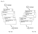
FIG. 1(a) is a view that illustrates a basic structure of an IPS mode liquid crystal display for O-Mode according to the present invention; and -
FIG. 1(b) is a view that illustrates a basic structure of an IPS mode liquid crystal display for E-Mode according to the present invention. - Hereinafter, the present invention will be described in detail.
- A liquid crystal panel according to the present invention may be an O mode, or E mode. The O mode liquid crystal panel means a mode in which an absorption axis direction of a polarizer that is disposed at the backlight side of the liquid crystal cell and the alignment direction of the liquid crystal cell are parallel to each other. The E mode liquid crystal panel means a mode in which an absorption axis direction of the polarizer that is disposed at the backlight side of the liquid crystal cell and the alignment direction of the liquid crystal cell are vertical to each other.
- With reference to
FIG. 1(a) , in the case of the O mode liquid crystal panel, it is preferable that a second polarizingplate 3, a positive biaxial film A and a negative C plate are disposed at an observer side of theliquid crystal cell 2, and the first polarizingplate 1 is disposed at the backlight side of the liquid crystal cell. With reference toFIG. 1(b) , in the E mode liquid crystal panel, it is preferable that the second polarizingplate 3 is disposed at the observer side of theliquid crystal cell 2, and the first polarizingplate 1, the positive biaxial film A and the negative C plate are disposed at the backlight side of theliquid crystal cell 2. - Therefore, the IPS mode liquid crystal display for O mode according to the present invention is characterized in that the first polarizing plate is disposed at the backlight side of the liquid crystal cell, and the second polarizing plate and the retardation film comprising the positive biaxial acryl-based film and the negative C plate are disposed at the observer side of the liquid crystal cell.
- In the IPS mode liquid crystal display for O mode, it is preferable that the absorption axis of the first polarizing plate and the absorption axis of the second polarizing plate are vertical to each other, the optical axis of the liquid crystal in the liquid crystal cell is parallel to the absorption axis of the first polarizing plate, and the optical axis of the positive biaxial acryl-based film is parallel to the absorption axis of the second polarizing plate, but it is not limited thereto.
- In addition, the IPS mode liquid crystal display for E mode according to the present invention is characterized in that the first polarizing plate and the retardation film comprising the positive biaxial acryl-based film and the negative C plate are disposed at the backlight side of the liquid crystal cell, and the second polarizing plate is disposed at the observer side of the liquid crystal cell.
- In the IPS mode liquid crystal display for E mode, it is preferable that the absorption axis of the first polarizing plate and the absorption axis of the second polarizing plate are vertical to each other, the optical axis of the liquid crystal in the liquid crystal cell is parallel to the absorption axis of the second polarizing plate, and the optical axis of the positive biaxial acryl-based film is parallel to the absorption axis of the first polarizing plate, but it is not limited thereto.
- In the IPS mode liquid crystal display according to the present invention, the positive biaxial acryl-based film of 3) may be produced by forming a film according to a melt extruding method or a solution casting method by using an acryl-based polymer and performing a TD (transverse direction) stretching process.
- The stretching process that is carried out while the positive biaxial acryl-based film of 3) is produced may carry out the TD stretching after the vertical uniaxial stretching or only the TD stretching. Since the TD stretching is carried out while both ends of the film are grasped by using grips during the stretching process, the biaxial stretching property can be shown, such that the biaxial stretching film can be produced.
- In more detail, the TD stretching process is carried out to increase the width of the film by using clips in a stretching process, and it may carry out a preheating step, a stretching step and a heat treatment step individually, and it may carry out the steps continuously. In the stretching step, in consideration of the glass transition temperature (Tg) of the acryl-based non-stretched film, within a temperature range of (Tg - 10°C) to (Tg + 10°C), a process can be carried out in a reverse direction of a progress direction of the film, that is, the TD stretching process can be carried out. The stretching temperature in the stretching process depends on the kind of used resin, but it is generally in the range of 80 to 250°C, preferably 100 to 200°C, and more preferably 110 to 160°C. In the stretching step, the stretching ratio may be set by the thickness of the non-stretched film and appropriate implementation of the retardation value, and it is preferable that the ratio is in the range of 1.1 to 4 times.
- It is preferable that the acryl-based polymer comprises the acryl-based copolymer that comprises the acryl-based monomer, aromatic vinyl monomer, maleic anhydride-based monomer and vinylcyan-based monomer.
- The acryl-based monomer that is disclosed in the present specification comprises acrylate and an acrylate derivative, and it is understood that it comprises alkyl acrylate, alkyl methacrylate, alkyl butacrylate or the like. For example, examples of the acryl-based monomer comprise a compound that is represented by the following Formula 1:


- In detail, as the acryl-based monomer, methyl methacrylate, ethyl methacrylate, propyl methacrylate, n-butyl methacrylate, t-butyl methacrylate, cyclohexyl methacrylate, benzyl methacrylate, methoxyethyl methacrylate, ethoxyethyl methacrylate, butoxymethyl methacrylate, and oligomers thereof may be used, but it is not limited thereto.
- It is preferable that the content of the acryl-based monomer in the acryl-based copolymer is in the range of 40 to 99 wt%. In the case of when the content of the acryl-based monomer is less than 40 wt%, high heat resistance and high transparency that are intrinsic properties of the acryl-based polymer may not be sufficiently implemented. In the case of when the content of the acryl-based monomer is more than 99 wt%, there is a problem in that mechanical strength is lowered.
- As the aromatic vinyl monomer of the acryl-based copolymer, there are styrene, α-methyl styrene, 4-methyl styrene and the like. Styrene is preferable, but the monomer is not limited thereto.
- It is preferable that the content of the aromatic vinyl monomer in the acryl-based copolymer is in the range of 1 to 60 wt%.
- It is preferable that the content of the maleic anhydride-based monomer in the acryl-based copolymer according to the present invention is in the range of 5 to 30 wt%. In the case of when the content of the maleic anhydride-based monomer is more than 30 wt%, since the brittleness of the film is increased, there is a problem in that the film is easily broken.
- As the maleic anhydride-based monomer of the acryl-based copolymer, there is maleic anhydride and the like, and as the vinylcyan-based monomer, there are acrylonitrile, methacrylonitrile, ethacrylonitrile and the like, but they are not limited thereto.
- It is preferable that the content of the vinylcyan-based monomer in the acryl-based copolymer is in the range of 0.1 to 10 wt%.
- The positive biaxial acryl-based film of 3) may further include the rubber component.
- In the present invention, the positive biaxial film means that a refractive index (nx) in a direction in which the refractive index is highest in a plane direction of the film, a refractive index (ny) in a direction that is vertical to the nx direction in the plane direction of the film, and a refractive index (nz) of the thickness satisfy the correlation of nz > nx > ny.
- It is preferable that the rubber component is an acryl rubber, a rubber-acryl-based graft type of core-shell polymer, or a mixture thereof, but it is not limited thereto.
- In the case of when the acryl-based resin has the refractive index that is similar to that of the rubber component, since the acryl rubber can obtain the thermoplastic resin composition that has excellent transparency, the acryl rubber is not particularly limited as long as the acryl rubber has the refractive index in the range of 1.480 to 1.550, which is similar to the refractive index of the acryl-based resin. For example, there are alkyl acrylate such as butyl acrylate, 2-ethylhexyl acrylate and the like. The rubber-acryl-based graft type of core-shell polymer is not particularly limited as long as it is the rubber-acryl-based graft type of core-shell polymer that has the refractive index in the range of 1.480 to 1.550. For example, particles in which the butadiene, butyl acryllate or butyl acryllate-styrene copolymer-based rubber is used as the core and polymethyl methacrylate or polystyrene is used as the shell and which has the size in the range of 50 to 400 nm may be used.
- The content of the rubber component is preferably in the range of 1 to 50 parts by weight, more preferably in the range of 10 to 30 parts by weight on the basis of 100 parts by weight of the acryl-based copolymer. In the case of when the content of the rubber component is less than 1 part by weight, it is impossible to implement excellent mechanical strength of the film, a problem in processing occurs because the film is easily broken, and the optical performance is not sufficiently implemented. In addition, in the case of when the content is higher than 30 parts by weight, there are problems in that the intrinsic high heat resistance and high transparency of the acryl-based copolymer are not sufficiently implemented, and in the stretching process, a haze occurs.
- In the positive biaxial acryl-based film of 3), it is preferable that the in-plane retardation value that is represented by the following
Equation 1 is in the range of 60 to 150 nm, and the thickness retardation value that is represented by the followingEquation 2 is in the range of 100 to 200 nm.

- wherein nx is a refractive index in a direction in which the refractive index is highest in a plane direction of the film,
- ny is a refractive index in a direction that is vertical to the nx direction in the plane direction of the film,
- nz is a refractive index of the thickness direction, and
- d is the thickness of the film.
- It is preferable that the glass transition temperature (Tg) of the positive biaxial acryl-based film of 3) is in the range of 100 to 250°C. The film that has the glass transition temperature (Tg) in the range of 100 to 250°C may have excellent durability.
- In addition, in the positive biaxial acryl-based film of 3), it is preferable that the in-plane retardation value that is represented by
Equation 1 and the thickness retardation value that is represented byEquation 2 satisfy the correlation of Rth > Rin. - In the IPS mode liquid crystal display according to the present invention, in order to minimize penetrating light in a dark state of the polarizing plate, the positive thickness retardation value is required. Since the positive biaxial acryl-based film that is used in the present invention has the Rth/Rin value that is larger than 1 while the stretching is carried out, it is necessary to reduce the Rth value.
- Accordingly, the present invention can control the Rth/Rin value of the entire retardation film by introducing the negative C plate into the positive biaxial acryl-based film.
- In the present invention, the negative C plate means that a refractive index (nx) in a direction in which the refractive index is highest in a plane direction of the film, a refractive index (ny) in a direction that is vertical to the nx direction in the plane direction of the film, and a refractive index (nz) of the thickness satisfy the correlation of nx≅ ny > nz.
- The negative C plate can be manufactured by manufacturing the 10 to 30 wt% of polymer solution using a material that has a negative retardation value in a thickness direction and high birefringence, and coating it on the positive biaxial acryl-based film in a thin film form. As the material that has the negative retardation value in a thickness direction and high birefringence, there is a compouned that comprises aromatic rings or cycloolefines at a main chain of the polymer. More detailed examples thereof may comprise polyarylate, polynorbornene, polycarbonate, polysulfone, polyimide, cellulose and a derivative thereof. The examples are preferably polyarylate and a cellulose derivative, but are not limited thereto.
- In particular, polyarylate may comprise a compound that is represented by the following
Formula 2.
- The negative C plate has the in-plane retardation value that is represented by
Equation 1 and in the range of preferably 0 to 10 nm, more preferably 0 to 5 nm, and most preferably 0 to 3 nm. In addition, the thickness retardation value that is represented byEquation 2 is in the range of -40 to -150 nm. - The IPS mode liquid crystal display according to the present invention uses a combination of the positive biaxial acryl-based film and the negative C plate as the retardation film, such that a wider viewing angle property can be implemented. That is, since the positive biaxial acryl-based film satisfies the correlation of Rth/Rin > 1 and can be controlled so as to satisfy the correlation of Rth/Rin < 1 by using the negative C plate that has the negative thickness retardation value, light leakage occurring in the polarizing plate and the IPS mode liquid crystal panel can be minimized.
- In particular, in the IPS mode liquid crystal display according to the present invention, it is more preferable that the Rth/Rin value of the acryl-based retardation film of 3) is in the range of 1.1 to 6.
- The acryl-based retardation film has the positive in-plane retardation value and the positive thickness retardation value while the stretching is carried out, but the ratio of two values becomes easily larger than 1. Therefore, when the IPS mode liquid crystal display using it is compared to the IPS mode liquid crystal display that does not use the viewing angle compensation film, there are problems in that there is no light leakage at an inclination angle but a relatively low constrast ratio value is ensured.
- In the IPS mode liquid crystal display according to the present invention, the in-plane retardation value, which is represented by
Equation 1, of 3) the entire retardation film comprising the positive biaxial acryl-based film and the negative C plate is in the range of preferably 60 to 150 nm, and the thickness retardation value that is represented byEquation 2 is in the range of more preferably 30 to 120 nm. - It is preferable that the thickness of the negative C plate is in the range of 0.5 to 30 µm, and the thickness of the entire retardation film comprising the positive biaxial acryl-based film and the negative C plate is in the range of 20 to 100 µm, but they are not limited thereto.
- In the IPS mode liquid crystal display according to the present invention, 3) the retardation film may further include a buffer layer between the positive biaxial acryl-based film and the negative C plate.
- The buffer layer may improve an adhesion strength between the positive biaxial acryl-based film and the negative C plate, and prevent a solvent corrosion in respects to a substrate. The buffer layer may comprise a compound that is selected from the group consisting of a UV curable or thermal curable acrylate polymer, a methacrylate polymer, and an acrylate/methacrylate copolymer, but is not limited thereto. In addition, the material may comprise pure polymer that is not cured, and as this material, there are a cellulose derivative, styrenes, anhydrides and a copolymer including them.
- The buffer layer may be formed in a range where a coating processing property is good while the solvent is not precipitated, and in detail, the thickness of the buffer layer may be in the range of 0.2 to 3 µm.
- In addition, 3) the retardation film may further include the adhesive layer between the positive biaxial acryl-based film and the negative C plate.
- The adhesive layer may be implemented through the coating on the negative C plate layer, or may be attached to the acryl-based film through the transferring. The adhesive layer may be selected from the group consisting of natural rubber, synthetic rubber or elastomer, vinyl chloride/vinyl acetate copolymer, polyvinylalkyl ether, polyacrylate, modified polyolefine-based compounds, and a compound comprising a curing agent such as isocyanate, but is not limited thereto.
- In addition, the optical axis of the positive biaxial acryl-based film is characterized in that the optical axis is parallel to the absorption axis of 4) the second polarizing plate. In the case of when the optical axis of the positive biaxial acryl-based film is not parallel to the absorption axis of 4) the second polarizing plate, a light leakage phenomenon may occur by light leakage between the first polarizing plate and the second polarizing plate at an inclination angle on an optical path.
- In the IPS mode liquid crystal display according to the present invention, the absorption axis of 1) first polarizing plate is vertical to the absorption axis of 4) the second polarizing plate.
- 1) the first polarizing plate and 4) the second polarizing plate comprises a polarizing element. As the polarizing element, a film that comprises polyvinyl alcohol (PVA) having iodine or dichromatic dyes may be used. The polarizing element may be manufactured by dyeing the iodine or dichromatic dyes on the PVA film, but the manufacturing method thereof is not particularly limited.
- 1) the first polarizing plate and 4) the second polarizing plate may comprise a protective film on any one side or both sides of the polarizing element.
- As the protective film, there are a triacetate cellulose (TAC) film, a polynorbornene-based film that is manufactured by using ring opening metathesis polymerization (ROMP), a HROMP (ring opening metathesis polymerization followed by hydrogenation) polymer film that is obtained by rehydrogenating the ring-opened cyclic olefine-based polymer, a polyester film, or a polynorbornene-based film that is manufactured by using the addition polymerization. In addition to this, the film that is made of a transparent polymer material may be used as the protective film, but it is not limited thereto.
- In the IPS mode liquid crystal display according to the present invention, 3) the retardation film may be disposed between 4) the second polarizing plate and 2) the liquid crystal cell, and the negative C plate of 3) the retardation film may be disposed so that the negative C plate is adjacent to 2) the liquid crystal cell.
- Hereinbelow, the present invention will be described in detail with reference to the drawings.
-
FIG. 1(a) illustrates a basic structure of the IPS mode liquid crystal display. - The IPS mode liquid crystal display comprises the first
polarizing plate 1, the secondpolarizing plate 3, and theliquid crystal cell 2, the absorption axis of the firstpolarizing plate 1 is disposed so that the absorption axis is vertical to the absorption axis of the secondpolarizing plate 3, the absorption axis of the secondpolarizing plate 3 is disposed so that the absorption axis is parallel to the optical axis of the positive biaxial acryl-based film A, and the negative C plate layer is disposed between the positive biaxial acryl-based film A and theliquid crystal cell 2. The buffer layer that has no in-plane and thickness retardation values may be disposed between the positive biaxial acryl-based film A and the negative C plate layer, and may further include the adhesive layer. - A better understanding of the present invention may be obtained in light of the following preferable Examples which are set forth to illustrate, but are not to be construed to limit the present invention.
- The IPS mode liquid crystal display that was used in Examples 1 to 5 included the IPS liquid crystal cell in which the liquid crystal having the cell gap of 2.9 µm, the pretilt angle of 3°, the dielectric anisotropic property Δε of 7, the birefringence Δn of 0.1 was filled.
- As the positive biaxial acryl-based film, the film that had the thickness of about 200 µm was formed by using the extruder that had the diameter of 60 Φ and L/D of 32 so that the component content ratio (wt%) of methylmethacrylate:styrene:maleic anhydride:acrylonitrile (MMA:SM:MAH:AN) is 65:24:10:1. After the formed film was stretched using the TD stretching machine at 120°C by 250 to 350%, the stretched film that had the in-plane retardation value (Rin) in the range of 90 to 130 nm and the thickness retardation value (Rth) in the range of 130 to 160 nm was manufactured.
- To manufacture the negative C plate, polyarylate (Unitica Co., U-100) was dissolved in 7.5 wt% of dichloroethane, coated on the uniaxially stretched acryl-based copolymer film by using the bar-coater, and dried in the convection oven at 80°C for 3 min.
- The polarizing plate was combined in the order as shown in
FIG. 1(a) for the combination of each retardation value, and combined with the IPS mode liquid crystal display panel, and the contrast ratio was measured at the inclination angle of 60° using Eldim to compare the clearness of the image. The second polarizing plate was attached with the polarizing plate that was combined in the order of ORT (zero retardation TAC)/PVA/TAC in Examples and Comparative Examples. - Comparative Example 1 carried out the comparison by attaching the polarizing plate in which the first polarizing plate and the second polarizing plate were combined with each other in the order of ORT/PVA/TAC.
- The contrast ratio value is an indicator that displays the clearness of the image, and it is possible to implemente the clear image as the contrast ratio value is increased. Accordingly, in the present invention, the clearness of the image was compared by using the contrast property at the inclination angle of 60°.
- The test result values of Examples 1 to 5 and Comparative Example 1 are described in the following Table 1.
[Table 1] Positive biaxial film Negative C plate Contrast ratio at inclination angle of 60° Rin Rth Rth Thickness (nm) (nm) (nm) (µm) Example 1 100 130 -40 1.7 50:1 Example 2 110 150 -60 2.7 70:1 Example 3 120 160 -80 4.0 100:1 Example 4 120 160 -100 6.2 140:1 Example 5 120 160 -120 10.4 180:1 Comparative Example 1 120 125 - - 20:1 - The contrast ratio at inclination angle of 60° is a contrast ratio value at an upward direction angle of 45°.
- From the results of Table 1, it can be seen that the contrast ratio values of Examples 1 to 5 according to the present invention are in the range of 50 to 180:1, and values that are much better than 20:1 which is a contrast ratio value of Comparative Example 1 are ensured. Since the contrast ratio value is an index displaying the clearness of the image, the liquid crystal display according to the present invention can implement the clearer image.
- The IPS mode liquid crystal display according to the present invention can improve the contrast properties at the front side and at the inclination angle, and thus the clear image of the liquid crystal display can be implemented.
Claims (22)
- An IPS (in-plane switching) mode liquid crystal display, comprising:1) a first polarizing plate;2) a liquid crystal cell;3) a retardation film comprising a positive biaxial acryl-based film and a negative C plate; and4) a second polarizing plate.
- The IPS (in-plane switching) mode liquid crystal display as set forth in claim 1, wherein the first polarizing plate is disposed at a backlight side of the liquid crystal cell, and the second polarizing plate and the retardation film comprising the positive biaxial acryl-based film and the negative C plate are disposed at an observer side of the liquid crystal cell.
- The IPS (in-plane switching) mode liquid crystal display as set forth in claim 2, wherein an absorption axis of the first polarizing plate and an absorption axis of the second polarizing plate are vertical, an optical axis of the liquid crystal in the liquid crystal cell is parallel to an absorption axis of the first polarizing plate, and an optical axis of the positive biaxial acryl-based film is parallel to the absorption axis of the second polarizing plate.
- The IPS (in-plane switching) mode liquid crystal display as set forth in claim 1, wherein the first polarizing plate and the retardation film that includes the positive biaxial acryl-based film and the negative C plate are disposed at the backlight side of the liquid crystal cell, and the second polarizing plate is disposed at the observer side of the liquid crystal cell.
- The IPS (in-plane switching) mode liquid crystal display as set forth in claim 4, wherein an absorption axis of the first polarizing plate and an absorption axis of the second polarizing plate are vertical, an optical axis of the liquid crystal in the liquid crystal cell is parallel to an absorption axis of the second polarizing plate, and an optical axis of the positive biaxial acryl-based film is parallel to the absorption axis of the first polarizing plate.
- The IPS (in-plane switching) mode liquid crystal display as set forth in claim 1, wherein the positive biaxial acryl-based film of 3) is produced by forming a film according to a melt extruding method or a solution casting method by using an acryl-based polymer and performing a TD (transverse direction) stretching process.
- The IPS (in-plane switching) mode liquid crystal display as set forth in claim 1, wherein the positive biaxial acryl-based film of 3) comprises an acryl-based copolymer that comprises an acryl-based monomer, an aromatic vinyl monomer, a maleic anhydride-based monomer and a vinylcyan-based monomer.
- The IPS (in-plane switching) mode liquid crystal display as set forth in claim 1, wherein the positive biaxial acryl-based film of 3) includes a rubber component.
- The IPS (in-plane switching) mode liquid crystal display as set forth in claim 1, wherein in the positive biaxial acryl-based film of 3), the in-plane retardation value that is represented by the following Equation 1 is in the range of 60 to 150 nm, and the thickness retardation value that is represented by the following Equation 2 is in the range of 100 to 200 nm:


wherein nx is a refractive index in a direction in which the refractive index is highest in a plane direction of the film,
ny is a refractive index in a direction that is vertical to the nx direction in the plane direction of the film,
nz is a refractive index of the thickness direction, and
d is the thickness of the film. - The IPS (in-plane switching) mode liquid crystal display as set forth in claim 1, wherein in the positive biaxial acryl-based film of 3), the in-plane retardation value that is represented by the following Equation 1 and the thickness retardation value that is represented by the following Equation 2 has the correlation of Rth > Rin:

 wherein nx is a refractive index in a direction in which the refractive index is highest in a plane direction of the film,ny is a refractive index in a direction that is vertical to the nx direction in the plane direction of the film,nz is a refractive index of the thickness direction, andd is the thickness of the film.
 - The IPS (in-plane switching) mode liquid crystal display as set forth in claim 1, wherein the negative C plate of 3) comprises one or more that are selected from the group consisting of polyarylate, polynorbornene, polycarbonate, polysulfone, polyimide, cellulose and a derivative thereof.
- The IPS (in-plane switching) mode liquid crystal display as set forth in claim 1, wherein in the negative C plate of 3), the in-plane retardation value that is represented by the following Equation 1 is in the range of 0 to 10 nm, and the thickness retardation value that is represented by the following Equation 2 is in the range of -40 to -150 nm:
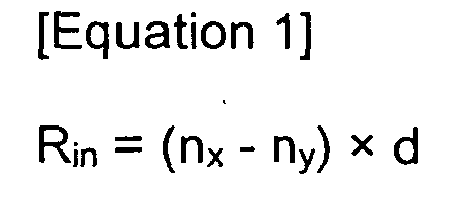
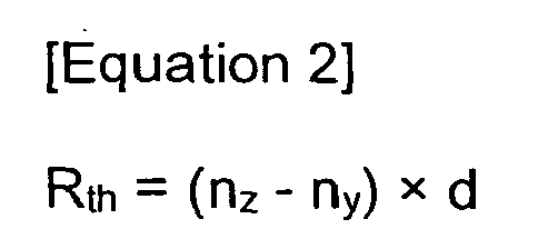 wherein nx is a refractive index in a direction in which the refractive index is highest in a plane direction of the film,ny is a refractive index in a direction that is vertical to the nx direction in the plane direction of the film,nz is a refractive index of the thickness direction, andd is the thickness of the film.
 - The IPS (in-plane switching) mode liquid crystal display as set forth in claim 1, wherein the thickness of the negative C plate of 3) is in the range of 1 to 30 µm.
- The IPS (in-plane switching) mode liquid crystal display as set forth in claim 1, wherein the thickness of 3) the retardation film is in the range of 20 to 100 µm.
- The IPS (in-plane switching) mode liquid crystal display as set forth in claim 1, wherein in 3) the retardation film comprising the positive biaxial acryl-based film and the negative C plate, the in-plane retardation value that is represented by the following Equation 1 is in the range of 60 to 150 nm, and the thickness retardation value that is represented by the following Equation 2 is in the range of 30 to 120 nm:

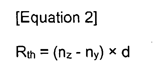 wherein nx is a refractive index in a direction in which the refractive index is highest in a plane direction of the film,ny is a refractive index in a direction that is vertical to the nx direction in the plane direction of the film,nz is a refractive index of the thickness direction, andd is the thickness of the film.
 - The IPS (in-plane switching) mode liquid crystal display as set forth in claim 1, wherein the Rth/Rin value of 3) the retardation film is in the range of 1.1 to 6.
- The IPS (in-plane switching) mode liquid crystal display as set forth in claim 1, wherein 3) the retardation film further comprises a buffer layer between the positive biaxial acryl-based film and the negative C plate.
- The IPS (in-plane switching) mode liquid crystal display as set forth in claim 1, wherein 3) the retardation film further comprises an adhesive layer between the positive biaxial acryl-based film and the negative C plate.
- The IPS (in-plane switching) mode liquid crystal display as set forth in claim 18, wherein the adhesive layer is coated on the negative C plate layer or transferred on the acryl-based film.
- The IPS (in-plane switching) mode liquid crystal display as set forth in claim 1, wherein 3) the retardation film is disposed between 4) the second polarizing plate and 2) the liquid crystal cell, the negative C plate of 3) the retardation film is disposed to contact with 2) the liquid crystal cell.
- The IPS (in-plane switching) mode liquid crystal display as set forth in claim 1, wherein 4) the second polarizing plate comprises a polarizing element, and further comprises a protective film between the polarizing element and the positive biaxial acryl-based film.
- The IPS (in-plane switching) mode liquid crystal display as set forth in claim 1, wherein 2) the liquid crystal cell comprises the liquid crystal that has the positive dielectric anisotropic property (Δε > 0), and is horizontally aligned.
Applications Claiming Priority (2)
| Application Number | Priority Date | Filing Date | Title |
|---|---|---|---|
| KR1020080083830A KR101197162B1 (en) | 2008-08-27 | 2008-08-27 | In-plane swiching mode liquid crystal display |
| PCT/KR2009/004731 WO2010024573A2 (en) | 2008-08-27 | 2009-08-25 | In-plane switching mode liquid crystal display |
Publications (3)
| Publication Number | Publication Date |
|---|---|
| EP2322980A2 true EP2322980A2 (en) | 2011-05-18 |
| EP2322980A4 EP2322980A4 (en) | 2011-08-24 |
| EP2322980B1 EP2322980B1 (en) | 2012-12-26 |
Family
ID=41722097
Family Applications (1)
| Application Number | Title | Priority Date | Filing Date |
|---|---|---|---|
| EP09810178A Active EP2322980B1 (en) | 2008-08-27 | 2009-08-25 | In-plane switching mode liquid crystal display |
Country Status (7)
| Country | Link |
|---|---|
| US (1) | US8243239B2 (en) |
| EP (1) | EP2322980B1 (en) |
| JP (1) | JP5376473B2 (en) |
| KR (1) | KR101197162B1 (en) |
| CN (1) | CN102132199B (en) |
| TW (1) | TWI395018B (en) |
| WO (1) | WO2010024573A2 (en) |
Families Citing this family (26)
| Publication number | Priority date | Publication date | Assignee | Title |
|---|---|---|---|---|
| KR101314480B1 (en) * | 2008-12-26 | 2013-10-07 | 주식회사 엘지화학 | Polarizer for ips mode lcd and ips mode lcd comprising the same |
| WO2012008326A1 (en) * | 2010-07-12 | 2012-01-19 | ソニー株式会社 | Method for manufacturing a master plate, method for manufacturing an oriented film, method for manufacturing a retardation plate, and method for manufacturing a display device |
| JP5576238B2 (en) * | 2010-10-25 | 2014-08-20 | 京セラディスプレイ株式会社 | Liquid crystal display |
| KR101304591B1 (en) * | 2011-07-06 | 2013-09-05 | 주식회사 엘지화학 | Retardation film, preparation method thereof, and liquid crystal display comprising the same |
| US9315412B2 (en) * | 2011-07-07 | 2016-04-19 | Corning Incorporated | Surface flaw modification for strengthening of glass articles |
| CN102636920A (en) * | 2011-07-19 | 2012-08-15 | 京东方科技集团股份有限公司 | Hard-screen liquid crystal display device, implementation method and application of hard-screen liquid crystal display device |
| TWI516537B (en) * | 2011-10-04 | 2016-01-11 | Lg化學股份有限公司 | Resin composition and optical compensation film formed by using the same |
| KR101418755B1 (en) | 2011-10-05 | 2014-07-11 | 주식회사 엘지화학 | Resin Compositions For Optical Film And Optical Compensation Films Formed By Using The Same |
| CN102681248A (en) * | 2012-05-10 | 2012-09-19 | 京东方科技集团股份有限公司 | Liquid crystal display |
| TWI530717B (en) * | 2012-12-17 | 2016-04-21 | 第一毛織股份有限公司 | Polarizing plate, method of preparing the same, and liquid crystal display apparatus including the same |
| KR102078021B1 (en) * | 2012-12-31 | 2020-02-17 | 엘지디스플레이 주식회사 | polarizer, manufacturing method thereof, and liquid crystal display including the same |
| KR102101794B1 (en) | 2013-07-17 | 2020-04-20 | 삼성디스플레이 주식회사 | Liquid crystal display |
| KR101708967B1 (en) * | 2013-09-30 | 2017-02-21 | 주식회사 엘지화학 | Retadation film and preparing method for retadation film |
| KR101640970B1 (en) * | 2013-09-30 | 2016-07-19 | 주식회사 엘지화학 | Retadation film and preparing method for retadation film |
| KR101727361B1 (en) * | 2014-05-21 | 2017-04-14 | 주식회사 엘지화학 | Retardation film and preparing method for the same |
| KR101725592B1 (en) * | 2014-08-14 | 2017-04-10 | 주식회사 엘지화학 | Retadation film and preparing method for retadation film |
| KR101725591B1 (en) * | 2014-08-14 | 2017-04-10 | 주식회사 엘지화학 | Retadation film and preparing method for retadation film |
| KR101725590B1 (en) * | 2014-08-14 | 2017-04-10 | 주식회사 엘지화학 | Retadation film and preparing method for retadation film |
| KR101725593B1 (en) * | 2014-08-14 | 2017-04-10 | 주식회사 엘지화학 | Retadation film and preparing method for retadation film |
| KR101724797B1 (en) * | 2014-08-14 | 2017-04-07 | 주식회사 엘지화학 | Retadation film and preparing method for retadation film |
| JP2017198774A (en) * | 2016-04-26 | 2017-11-02 | スタンレー電気株式会社 | Liquid crystal display device |
| CN106154639B (en) | 2016-09-29 | 2020-01-10 | 厦门天马微电子有限公司 | Liquid crystal display panel and liquid crystal display device |
| KR102134948B1 (en) * | 2017-12-21 | 2020-07-16 | 주식회사 엘지화학 | Optical film and polarizer plate comprising the same |
| KR102167213B1 (en) * | 2018-06-01 | 2020-10-20 | 주식회사 엘지화학 | Liquid Crystal Display Device |
| KR102143271B1 (en) * | 2018-06-05 | 2020-08-10 | 주식회사 엘지화학 | Laminate and liquid crystal display comprising the same |
| KR102625542B1 (en) * | 2018-11-20 | 2024-01-15 | 엘지디스플레이 주식회사 | Electroluminescence display device |
Family Cites Families (14)
| Publication number | Priority date | Publication date | Assignee | Title |
|---|---|---|---|---|
| KR100223601B1 (en) * | 1997-05-29 | 1999-10-15 | 윤종용 | Lcd device |
| TWI242083B (en) * | 2003-08-11 | 2005-10-21 | Sony Corp | Liquid crystal display device |
| KR100601916B1 (en) * | 2003-11-21 | 2006-07-14 | 주식회사 엘지화학 | Planar switching liquid crystal display comprising a viewing angle compensation film using a positive biaxial retardation film |
| KR100601920B1 (en) * | 2004-01-09 | 2006-07-14 | 주식회사 엘지화학 | Planar switching liquid crystal display including negative biaxial retardation film and viewing angle compensation film using + C-plate |
| US7400371B2 (en) * | 2004-02-03 | 2008-07-15 | Sumitomo Chemical Company, Limited | Liquid crystal display having particular retardation plate |
| JP2005321528A (en) * | 2004-05-07 | 2005-11-17 | Fuji Photo Film Co Ltd | Liquid crystal display |
| JP3851919B2 (en) * | 2004-12-20 | 2006-11-29 | 日東電工株式会社 | Liquid crystal panel and liquid crystal display device |
| JP3883134B2 (en) * | 2005-01-25 | 2007-02-21 | 日東電工株式会社 | Liquid crystal display |
| EP1850155B1 (en) * | 2005-02-08 | 2012-11-14 | Nippon Oil Corporation | Homeotropically oriented liquid-crystal film, optical film comprising the same, and image display |
| US7605895B2 (en) * | 2005-06-14 | 2009-10-20 | Lg Chem, Ltd. | IPS mode liquid crystal display using two sheets of biaxial negative retardation film and a plate |
| US7671945B2 (en) * | 2005-09-30 | 2010-03-02 | Teledyne Scientific & Imaging, Llc | UV curable alignment material for fabrication of monolithic compensators for liquid crystal displays |
| JP2007279127A (en) * | 2006-04-03 | 2007-10-25 | Nitto Denko Corp | Liquid crystal panel, liquid crystal television, and liquid crystal display device |
| US7751006B2 (en) * | 2006-09-29 | 2010-07-06 | Dai Nippon Printing Co., Ltd. | Optical element, liquid crystal display device member with the optical element, liquid crystal display device with the liquid crystal display device member, method of producing the optical element and method of evaluating birefringence functional layer |
| KR100964786B1 (en) | 2006-10-23 | 2010-06-21 | 주식회사 엘지화학 | Optical film, retardation film, and liquid crystal display including the same |
-
2008
- 2008-08-27 KR KR1020080083830A patent/KR101197162B1/en active Active
-
2009
- 2009-08-25 JP JP2011524897A patent/JP5376473B2/en active Active
- 2009-08-25 EP EP09810178A patent/EP2322980B1/en active Active
- 2009-08-25 CN CN2009801334435A patent/CN102132199B/en active Active
- 2009-08-25 WO PCT/KR2009/004731 patent/WO2010024573A2/en not_active Ceased
- 2009-08-26 US US12/461,864 patent/US8243239B2/en active Active
- 2009-08-27 TW TW098128775A patent/TWI395018B/en active
Also Published As
| Publication number | Publication date |
|---|---|
| WO2010024573A9 (en) | 2010-09-10 |
| EP2322980A4 (en) | 2011-08-24 |
| CN102132199A (en) | 2011-07-20 |
| KR20100025171A (en) | 2010-03-09 |
| JP5376473B2 (en) | 2013-12-25 |
| CN102132199B (en) | 2013-11-13 |
| JP2012501464A (en) | 2012-01-19 |
| KR101197162B1 (en) | 2012-11-09 |
| US20100053508A1 (en) | 2010-03-04 |
| TW201015160A (en) | 2010-04-16 |
| EP2322980B1 (en) | 2012-12-26 |
| TWI395018B (en) | 2013-05-01 |
| WO2010024573A2 (en) | 2010-03-04 |
| US8243239B2 (en) | 2012-08-14 |
| WO2010024573A3 (en) | 2010-07-08 |
Similar Documents
| Publication | Publication Date | Title |
|---|---|---|
| EP2322980B1 (en) | In-plane switching mode liquid crystal display | |
| JP5330502B2 (en) | Optical film and information electronic device including the same | |
| CN101210975B (en) | Laminate, liquid crystal panel, and liquid crystal display apparatus | |
| US8512822B2 (en) | Retardation film, method for manufacturing the same, and liquid crystal display device including the same | |
| KR101304591B1 (en) | Retardation film, preparation method thereof, and liquid crystal display comprising the same | |
| JP5888757B2 (en) | Retardation film, method for producing retardation film, liquid crystal display device and integrated polarizing plate | |
| KR101188755B1 (en) | In-plane swiching mode liquid crystal display | |
| KR20150033623A (en) | Retardation film for in-plane swiching mode liquid crystal display and liquid crystal display comprising the same | |
| KR20140000431A (en) | Retardation film and liquid crystal display including the same | |
| KR20130005774A (en) | Retardation film for in-plane swiching mode liquid crystal display and liquid crystal display comprising the same | |
| US9670352B2 (en) | Retardation film and a liquid-crystal display device comprising the same | |
| KR101243716B1 (en) | Retardation films having excellent adhesive property and liquid crystal display comprising the sames | |
| KR20070113749A (en) | Optically anisotropic film excellent in transparency and heat resistance and a liquid crystal display device comprising the same | |
| CN100407001C (en) | Liquid crystal panel and liquid crystal display device | |
| KR20090090553A (en) | Retardation film, manufacturing method thereof, and liquid crystal display including the same | |
| KR101260513B1 (en) | Optical film, polarizing plate and liquid crystal display comprising the same | |
| GB2272779A (en) | Optically anisotropic element | |
| TWI922747B (en) | Polarizing plate with phase difference layer and image display device | |
| KR102681962B1 (en) | Retardation film and method for manufacturing thereof |
Legal Events
| Date | Code | Title | Description |
|---|---|---|---|
| PUAI | Public reference made under article 153(3) epc to a published international application that has entered the european phase |
Free format text: ORIGINAL CODE: 0009012 |
|
| 17P | Request for examination filed |
Effective date: 20110217 |
|
| AK | Designated contracting states |
Kind code of ref document: A2 Designated state(s): AT BE BG CH CY CZ DE DK EE ES FI FR GB GR HR HU IE IS IT LI LT LU LV MC MK MT NL NO PL PT RO SE SI SK SM TR |
|
| AX | Request for extension of the european patent |
Extension state: AL BA RS |
|
| RIN1 | Information on inventor provided before grant (corrected) |
Inventor name: LEE, MIN-HEE Inventor name: CHO, SAE-HAN Inventor name: CHOI, JEONG-MIN |
|
| A4 | Supplementary search report drawn up and despatched |
Effective date: 20110722 |
|
| RIC1 | Information provided on ipc code assigned before grant |
Ipc: G02F 1/1335 20060101AFI20110718BHEP |
|
| DAX | Request for extension of the european patent (deleted) | ||
| RIC1 | Information provided on ipc code assigned before grant |
Ipc: G02F 1/1335 20060101AFI20120417BHEP Ipc: G02F 1/13363 20060101ALI20120417BHEP |
|
| GRAP | Despatch of communication of intention to grant a patent |
Free format text: ORIGINAL CODE: EPIDOSNIGR1 |
|
| GRAS | Grant fee paid |
Free format text: ORIGINAL CODE: EPIDOSNIGR3 |
|
| GRAA | (expected) grant |
Free format text: ORIGINAL CODE: 0009210 |
|
| AK | Designated contracting states |
Kind code of ref document: B1 Designated state(s): AT BE BG CH CY CZ DE DK EE ES FI FR GB GR HR HU IE IS IT LI LT LU LV MC MK MT NL NO PL PT RO SE SI SK SM TR |
|
| REG | Reference to a national code |
Ref country code: GB Ref legal event code: FG4D |
|
| REG | Reference to a national code |
Ref country code: CH Ref legal event code: EP |
|
| REG | Reference to a national code |
Ref country code: AT Ref legal event code: REF Ref document number: 590769 Country of ref document: AT Kind code of ref document: T Effective date: 20130115 |
|
| REG | Reference to a national code |
Ref country code: DE Ref legal event code: R096 Ref document number: 602009012341 Country of ref document: DE Effective date: 20130314 |
|
| PG25 | Lapsed in a contracting state [announced via postgrant information from national office to epo] |
Ref country code: SE Free format text: LAPSE BECAUSE OF FAILURE TO SUBMIT A TRANSLATION OF THE DESCRIPTION OR TO PAY THE FEE WITHIN THE PRESCRIBED TIME-LIMIT Effective date: 20121226 Ref country code: NO Free format text: LAPSE BECAUSE OF FAILURE TO SUBMIT A TRANSLATION OF THE DESCRIPTION OR TO PAY THE FEE WITHIN THE PRESCRIBED TIME-LIMIT Effective date: 20130326 Ref country code: HR Free format text: LAPSE BECAUSE OF FAILURE TO SUBMIT A TRANSLATION OF THE DESCRIPTION OR TO PAY THE FEE WITHIN THE PRESCRIBED TIME-LIMIT Effective date: 20121226 Ref country code: FI Free format text: LAPSE BECAUSE OF FAILURE TO SUBMIT A TRANSLATION OF THE DESCRIPTION OR TO PAY THE FEE WITHIN THE PRESCRIBED TIME-LIMIT Effective date: 20121226 Ref country code: LT Free format text: LAPSE BECAUSE OF FAILURE TO SUBMIT A TRANSLATION OF THE DESCRIPTION OR TO PAY THE FEE WITHIN THE PRESCRIBED TIME-LIMIT Effective date: 20121226 |
|
| REG | Reference to a national code |
Ref country code: AT Ref legal event code: MK05 Ref document number: 590769 Country of ref document: AT Kind code of ref document: T Effective date: 20121226 |
|
| REG | Reference to a national code |
Ref country code: LT Ref legal event code: MG4D |
|
| REG | Reference to a national code |
Ref country code: NL Ref legal event code: VDEP Effective date: 20121226 |
|
| PG25 | Lapsed in a contracting state [announced via postgrant information from national office to epo] |
Ref country code: SI Free format text: LAPSE BECAUSE OF FAILURE TO SUBMIT A TRANSLATION OF THE DESCRIPTION OR TO PAY THE FEE WITHIN THE PRESCRIBED TIME-LIMIT Effective date: 20121226 Ref country code: LV Free format text: LAPSE BECAUSE OF FAILURE TO SUBMIT A TRANSLATION OF THE DESCRIPTION OR TO PAY THE FEE WITHIN THE PRESCRIBED TIME-LIMIT Effective date: 20121226 Ref country code: GR Free format text: LAPSE BECAUSE OF FAILURE TO SUBMIT A TRANSLATION OF THE DESCRIPTION OR TO PAY THE FEE WITHIN THE PRESCRIBED TIME-LIMIT Effective date: 20130327 |
|
| PG25 | Lapsed in a contracting state [announced via postgrant information from national office to epo] |
Ref country code: AT Free format text: LAPSE BECAUSE OF FAILURE TO SUBMIT A TRANSLATION OF THE DESCRIPTION OR TO PAY THE FEE WITHIN THE PRESCRIBED TIME-LIMIT Effective date: 20121226 Ref country code: IS Free format text: LAPSE BECAUSE OF FAILURE TO SUBMIT A TRANSLATION OF THE DESCRIPTION OR TO PAY THE FEE WITHIN THE PRESCRIBED TIME-LIMIT Effective date: 20130426 Ref country code: EE Free format text: LAPSE BECAUSE OF FAILURE TO SUBMIT A TRANSLATION OF THE DESCRIPTION OR TO PAY THE FEE WITHIN THE PRESCRIBED TIME-LIMIT Effective date: 20121226 Ref country code: BE Free format text: LAPSE BECAUSE OF FAILURE TO SUBMIT A TRANSLATION OF THE DESCRIPTION OR TO PAY THE FEE WITHIN THE PRESCRIBED TIME-LIMIT Effective date: 20121226 Ref country code: ES Free format text: LAPSE BECAUSE OF FAILURE TO SUBMIT A TRANSLATION OF THE DESCRIPTION OR TO PAY THE FEE WITHIN THE PRESCRIBED TIME-LIMIT Effective date: 20130406 Ref country code: BG Free format text: LAPSE BECAUSE OF FAILURE TO SUBMIT A TRANSLATION OF THE DESCRIPTION OR TO PAY THE FEE WITHIN THE PRESCRIBED TIME-LIMIT Effective date: 20130326 Ref country code: SK Free format text: LAPSE BECAUSE OF FAILURE TO SUBMIT A TRANSLATION OF THE DESCRIPTION OR TO PAY THE FEE WITHIN THE PRESCRIBED TIME-LIMIT Effective date: 20121226 Ref country code: CZ Free format text: LAPSE BECAUSE OF FAILURE TO SUBMIT A TRANSLATION OF THE DESCRIPTION OR TO PAY THE FEE WITHIN THE PRESCRIBED TIME-LIMIT Effective date: 20121226 |
|
| PG25 | Lapsed in a contracting state [announced via postgrant information from national office to epo] |
Ref country code: PT Free format text: LAPSE BECAUSE OF FAILURE TO SUBMIT A TRANSLATION OF THE DESCRIPTION OR TO PAY THE FEE WITHIN THE PRESCRIBED TIME-LIMIT Effective date: 20130426 Ref country code: RO Free format text: LAPSE BECAUSE OF FAILURE TO SUBMIT A TRANSLATION OF THE DESCRIPTION OR TO PAY THE FEE WITHIN THE PRESCRIBED TIME-LIMIT Effective date: 20121226 Ref country code: NL Free format text: LAPSE BECAUSE OF FAILURE TO SUBMIT A TRANSLATION OF THE DESCRIPTION OR TO PAY THE FEE WITHIN THE PRESCRIBED TIME-LIMIT Effective date: 20121226 Ref country code: PL Free format text: LAPSE BECAUSE OF FAILURE TO SUBMIT A TRANSLATION OF THE DESCRIPTION OR TO PAY THE FEE WITHIN THE PRESCRIBED TIME-LIMIT Effective date: 20121226 |
|
| PG25 | Lapsed in a contracting state [announced via postgrant information from national office to epo] |
Ref country code: DK Free format text: LAPSE BECAUSE OF FAILURE TO SUBMIT A TRANSLATION OF THE DESCRIPTION OR TO PAY THE FEE WITHIN THE PRESCRIBED TIME-LIMIT Effective date: 20121226 |
|
| PLBE | No opposition filed within time limit |
Free format text: ORIGINAL CODE: 0009261 |
|
| STAA | Information on the status of an ep patent application or granted ep patent |
Free format text: STATUS: NO OPPOSITION FILED WITHIN TIME LIMIT |
|
| PG25 | Lapsed in a contracting state [announced via postgrant information from national office to epo] |
Ref country code: CY Free format text: LAPSE BECAUSE OF FAILURE TO SUBMIT A TRANSLATION OF THE DESCRIPTION OR TO PAY THE FEE WITHIN THE PRESCRIBED TIME-LIMIT Effective date: 20121226 |
|
| 26N | No opposition filed |
Effective date: 20130927 |
|
| PG25 | Lapsed in a contracting state [announced via postgrant information from national office to epo] |
Ref country code: IT Free format text: LAPSE BECAUSE OF FAILURE TO SUBMIT A TRANSLATION OF THE DESCRIPTION OR TO PAY THE FEE WITHIN THE PRESCRIBED TIME-LIMIT Effective date: 20121226 |
|
| REG | Reference to a national code |
Ref country code: DE Ref legal event code: R097 Ref document number: 602009012341 Country of ref document: DE Effective date: 20130927 |
|
| REG | Reference to a national code |
Ref country code: CH Ref legal event code: PL |
|
| PG25 | Lapsed in a contracting state [announced via postgrant information from national office to epo] |
Ref country code: LI Free format text: LAPSE BECAUSE OF NON-PAYMENT OF DUE FEES Effective date: 20130831 Ref country code: CH Free format text: LAPSE BECAUSE OF NON-PAYMENT OF DUE FEES Effective date: 20130831 Ref country code: MC Free format text: LAPSE BECAUSE OF FAILURE TO SUBMIT A TRANSLATION OF THE DESCRIPTION OR TO PAY THE FEE WITHIN THE PRESCRIBED TIME-LIMIT Effective date: 20121226 |
|
| REG | Reference to a national code |
Ref country code: IE Ref legal event code: MM4A |
|
| PG25 | Lapsed in a contracting state [announced via postgrant information from national office to epo] |
Ref country code: IE Free format text: LAPSE BECAUSE OF NON-PAYMENT OF DUE FEES Effective date: 20130825 |
|
| PG25 | Lapsed in a contracting state [announced via postgrant information from national office to epo] |
Ref country code: SM Free format text: LAPSE BECAUSE OF FAILURE TO SUBMIT A TRANSLATION OF THE DESCRIPTION OR TO PAY THE FEE WITHIN THE PRESCRIBED TIME-LIMIT Effective date: 20121226 |
|
| PG25 | Lapsed in a contracting state [announced via postgrant information from national office to epo] |
Ref country code: TR Free format text: LAPSE BECAUSE OF FAILURE TO SUBMIT A TRANSLATION OF THE DESCRIPTION OR TO PAY THE FEE WITHIN THE PRESCRIBED TIME-LIMIT Effective date: 20121226 Ref country code: MT Free format text: LAPSE BECAUSE OF FAILURE TO SUBMIT A TRANSLATION OF THE DESCRIPTION OR TO PAY THE FEE WITHIN THE PRESCRIBED TIME-LIMIT Effective date: 20121226 |
|
| PG25 | Lapsed in a contracting state [announced via postgrant information from national office to epo] |
Ref country code: LU Free format text: LAPSE BECAUSE OF NON-PAYMENT OF DUE FEES Effective date: 20130825 Ref country code: MK Free format text: LAPSE BECAUSE OF FAILURE TO SUBMIT A TRANSLATION OF THE DESCRIPTION OR TO PAY THE FEE WITHIN THE PRESCRIBED TIME-LIMIT Effective date: 20121226 Ref country code: HU Free format text: LAPSE BECAUSE OF FAILURE TO SUBMIT A TRANSLATION OF THE DESCRIPTION OR TO PAY THE FEE WITHIN THE PRESCRIBED TIME-LIMIT; INVALID AB INITIO Effective date: 20090825 |
|
| REG | Reference to a national code |
Ref country code: FR Ref legal event code: PLFP Year of fee payment: 8 |
|
| REG | Reference to a national code |
Ref country code: FR Ref legal event code: PLFP Year of fee payment: 9 |
|
| REG | Reference to a national code |
Ref country code: FR Ref legal event code: PLFP Year of fee payment: 10 |
|
| PGFP | Annual fee paid to national office [announced via postgrant information from national office to epo] |
Ref country code: DE Payment date: 20250606 Year of fee payment: 17 |
|
| REG | Reference to a national code |
Ref country code: GB Ref legal event code: 732E Free format text: REGISTERED BETWEEN 20250918 AND 20250924 |
|
| PGFP | Annual fee paid to national office [announced via postgrant information from national office to epo] |
Ref country code: GB Payment date: 20250702 Year of fee payment: 17 |
|
| PGFP | Annual fee paid to national office [announced via postgrant information from national office to epo] |
Ref country code: FR Payment date: 20250703 Year of fee payment: 17 |
|
| REG | Reference to a national code |
Ref country code: DE Ref legal event code: R081 Ref document number: 602009012341 Country of ref document: DE Owner name: SHANJIN OPTOELECTRONICS (SUZHOU) CO., LTD., ZH, CN Free format text: FORMER OWNER: LG CHEM. LTD., SEOUL/SOUL, KR |