JP5576238B2 - Liquid crystal display - Google Patents
Liquid crystal display Download PDFInfo
- Publication number
- JP5576238B2 JP5576238B2 JP2010238742A JP2010238742A JP5576238B2 JP 5576238 B2 JP5576238 B2 JP 5576238B2 JP 2010238742 A JP2010238742 A JP 2010238742A JP 2010238742 A JP2010238742 A JP 2010238742A JP 5576238 B2 JP5576238 B2 JP 5576238B2
- Authority
- JP
- Japan
- Prior art keywords
- liquid crystal
- transparent substrate
- polarizing plate
- glass substrate
- display device
- Prior art date
- Legal status (The legal status is an assumption and is not a legal conclusion. Google has not performed a legal analysis and makes no representation as to the accuracy of the status listed.)
- Expired - Fee Related
Links
- 239000004973 liquid crystal related substance Substances 0.000 title claims description 399
- 239000000758 substrate Substances 0.000 claims description 656
- 238000010521 absorption reaction Methods 0.000 claims description 206
- 230000005684 electric field Effects 0.000 claims description 172
- 239000000853 adhesive Substances 0.000 claims description 116
- 230000001070 adhesive effect Effects 0.000 claims description 116
- 239000000463 material Substances 0.000 claims description 35
- 230000014509 gene expression Effects 0.000 claims description 17
- 230000002093 peripheral effect Effects 0.000 claims description 9
- 238000002347 injection Methods 0.000 claims description 8
- 239000007924 injection Substances 0.000 claims description 8
- 238000000016 photochemical curing Methods 0.000 claims description 3
- 239000011521 glass Substances 0.000 description 403
- 239000010410 layer Substances 0.000 description 345
- 239000010408 film Substances 0.000 description 76
- 230000010287 polarization Effects 0.000 description 59
- 238000010586 diagram Methods 0.000 description 29
- 230000000694 effects Effects 0.000 description 23
- 230000007935 neutral effect Effects 0.000 description 14
- 238000004519 manufacturing process Methods 0.000 description 9
- 238000005452 bending Methods 0.000 description 7
- 230000000007 visual effect Effects 0.000 description 7
- 238000000034 method Methods 0.000 description 6
- 238000004040 coloring Methods 0.000 description 5
- 239000006185 dispersion Substances 0.000 description 5
- 239000000470 constituent Substances 0.000 description 4
- 239000011347 resin Substances 0.000 description 4
- 229920005989 resin Polymers 0.000 description 4
- 229920001187 thermosetting polymer Polymers 0.000 description 4
- 239000011159 matrix material Substances 0.000 description 3
- 239000000203 mixture Substances 0.000 description 3
- 238000001723 curing Methods 0.000 description 2
- 238000010438 heat treatment Methods 0.000 description 2
- 230000003287 optical effect Effects 0.000 description 2
- 239000003566 sealing material Substances 0.000 description 2
- 239000002356 single layer Substances 0.000 description 2
- 230000005856 abnormality Effects 0.000 description 1
- 239000003990 capacitor Substances 0.000 description 1
- 239000002131 composite material Substances 0.000 description 1
- 239000004020 conductor Substances 0.000 description 1
- 230000008602 contraction Effects 0.000 description 1
- 210000002858 crystal cell Anatomy 0.000 description 1
- 230000007547 defect Effects 0.000 description 1
- 238000001514 detection method Methods 0.000 description 1
- 230000005611 electricity Effects 0.000 description 1
- 239000007788 liquid Substances 0.000 description 1
- 239000011120 plywood Substances 0.000 description 1
- 230000003068 static effect Effects 0.000 description 1
- 239000010409 thin film Substances 0.000 description 1
Images


Classifications
-
- G—PHYSICS
- G02—OPTICS
- G02F—OPTICAL DEVICES OR ARRANGEMENTS FOR THE CONTROL OF LIGHT BY MODIFICATION OF THE OPTICAL PROPERTIES OF THE MEDIA OF THE ELEMENTS INVOLVED THEREIN; NON-LINEAR OPTICS; FREQUENCY-CHANGING OF LIGHT; OPTICAL LOGIC ELEMENTS; OPTICAL ANALOGUE/DIGITAL CONVERTERS
- G02F1/00—Devices or arrangements for the control of the intensity, colour, phase, polarisation or direction of light arriving from an independent light source, e.g. switching, gating or modulating; Non-linear optics
- G02F1/01—Devices or arrangements for the control of the intensity, colour, phase, polarisation or direction of light arriving from an independent light source, e.g. switching, gating or modulating; Non-linear optics for the control of the intensity, phase, polarisation or colour
- G02F1/13—Devices or arrangements for the control of the intensity, colour, phase, polarisation or direction of light arriving from an independent light source, e.g. switching, gating or modulating; Non-linear optics for the control of the intensity, phase, polarisation or colour based on liquid crystals, e.g. single liquid crystal display cells
- G02F1/133—Constructional arrangements; Operation of liquid crystal cells; Circuit arrangements
- G02F1/1333—Constructional arrangements; Manufacturing methods
- G02F1/1335—Structural association of cells with optical devices, e.g. polarisers or reflectors
- G02F1/13363—Birefringent elements, e.g. for optical compensation
-
- G—PHYSICS
- G02—OPTICS
- G02F—OPTICAL DEVICES OR ARRANGEMENTS FOR THE CONTROL OF LIGHT BY MODIFICATION OF THE OPTICAL PROPERTIES OF THE MEDIA OF THE ELEMENTS INVOLVED THEREIN; NON-LINEAR OPTICS; FREQUENCY-CHANGING OF LIGHT; OPTICAL LOGIC ELEMENTS; OPTICAL ANALOGUE/DIGITAL CONVERTERS
- G02F1/00—Devices or arrangements for the control of the intensity, colour, phase, polarisation or direction of light arriving from an independent light source, e.g. switching, gating or modulating; Non-linear optics
- G02F1/01—Devices or arrangements for the control of the intensity, colour, phase, polarisation or direction of light arriving from an independent light source, e.g. switching, gating or modulating; Non-linear optics for the control of the intensity, phase, polarisation or colour
- G02F1/13—Devices or arrangements for the control of the intensity, colour, phase, polarisation or direction of light arriving from an independent light source, e.g. switching, gating or modulating; Non-linear optics for the control of the intensity, phase, polarisation or colour based on liquid crystals, e.g. single liquid crystal display cells
- G02F1/133—Constructional arrangements; Operation of liquid crystal cells; Circuit arrangements
- G02F1/1333—Constructional arrangements; Manufacturing methods
- G02F1/1343—Electrodes
- G02F1/134309—Electrodes characterised by their geometrical arrangement
- G02F1/134363—Electrodes characterised by their geometrical arrangement for applying an electric field parallel to the substrate, i.e. in-plane switching [IPS]
-
- G—PHYSICS
- G02—OPTICS
- G02F—OPTICAL DEVICES OR ARRANGEMENTS FOR THE CONTROL OF LIGHT BY MODIFICATION OF THE OPTICAL PROPERTIES OF THE MEDIA OF THE ELEMENTS INVOLVED THEREIN; NON-LINEAR OPTICS; FREQUENCY-CHANGING OF LIGHT; OPTICAL LOGIC ELEMENTS; OPTICAL ANALOGUE/DIGITAL CONVERTERS
- G02F1/00—Devices or arrangements for the control of the intensity, colour, phase, polarisation or direction of light arriving from an independent light source, e.g. switching, gating or modulating; Non-linear optics
- G02F1/01—Devices or arrangements for the control of the intensity, colour, phase, polarisation or direction of light arriving from an independent light source, e.g. switching, gating or modulating; Non-linear optics for the control of the intensity, phase, polarisation or colour
- G02F1/13—Devices or arrangements for the control of the intensity, colour, phase, polarisation or direction of light arriving from an independent light source, e.g. switching, gating or modulating; Non-linear optics for the control of the intensity, phase, polarisation or colour based on liquid crystals, e.g. single liquid crystal display cells
- G02F1/133—Constructional arrangements; Operation of liquid crystal cells; Circuit arrangements
- G02F1/1333—Constructional arrangements; Manufacturing methods
- G02F1/1335—Structural association of cells with optical devices, e.g. polarisers or reflectors
- G02F1/13363—Birefringent elements, e.g. for optical compensation
- G02F1/133634—Birefringent elements, e.g. for optical compensation the refractive index Nz perpendicular to the element surface being different from in-plane refractive indices Nx and Ny, e.g. biaxial or with normal optical axis
-
- G—PHYSICS
- G02—OPTICS
- G02F—OPTICAL DEVICES OR ARRANGEMENTS FOR THE CONTROL OF LIGHT BY MODIFICATION OF THE OPTICAL PROPERTIES OF THE MEDIA OF THE ELEMENTS INVOLVED THEREIN; NON-LINEAR OPTICS; FREQUENCY-CHANGING OF LIGHT; OPTICAL LOGIC ELEMENTS; OPTICAL ANALOGUE/DIGITAL CONVERTERS
- G02F1/00—Devices or arrangements for the control of the intensity, colour, phase, polarisation or direction of light arriving from an independent light source, e.g. switching, gating or modulating; Non-linear optics
- G02F1/01—Devices or arrangements for the control of the intensity, colour, phase, polarisation or direction of light arriving from an independent light source, e.g. switching, gating or modulating; Non-linear optics for the control of the intensity, phase, polarisation or colour
- G02F1/13—Devices or arrangements for the control of the intensity, colour, phase, polarisation or direction of light arriving from an independent light source, e.g. switching, gating or modulating; Non-linear optics for the control of the intensity, phase, polarisation or colour based on liquid crystals, e.g. single liquid crystal display cells
- G02F1/133—Constructional arrangements; Operation of liquid crystal cells; Circuit arrangements
- G02F1/1333—Constructional arrangements; Manufacturing methods
- G02F1/1335—Structural association of cells with optical devices, e.g. polarisers or reflectors
- G02F1/13363—Birefringent elements, e.g. for optical compensation
- G02F1/133638—Waveplates, i.e. plates with a retardation value of lambda/n
-
- G—PHYSICS
- G02—OPTICS
- G02F—OPTICAL DEVICES OR ARRANGEMENTS FOR THE CONTROL OF LIGHT BY MODIFICATION OF THE OPTICAL PROPERTIES OF THE MEDIA OF THE ELEMENTS INVOLVED THEREIN; NON-LINEAR OPTICS; FREQUENCY-CHANGING OF LIGHT; OPTICAL LOGIC ELEMENTS; OPTICAL ANALOGUE/DIGITAL CONVERTERS
- G02F1/00—Devices or arrangements for the control of the intensity, colour, phase, polarisation or direction of light arriving from an independent light source, e.g. switching, gating or modulating; Non-linear optics
- G02F1/01—Devices or arrangements for the control of the intensity, colour, phase, polarisation or direction of light arriving from an independent light source, e.g. switching, gating or modulating; Non-linear optics for the control of the intensity, phase, polarisation or colour
- G02F1/13—Devices or arrangements for the control of the intensity, colour, phase, polarisation or direction of light arriving from an independent light source, e.g. switching, gating or modulating; Non-linear optics for the control of the intensity, phase, polarisation or colour based on liquid crystals, e.g. single liquid crystal display cells
- G02F1/133—Constructional arrangements; Operation of liquid crystal cells; Circuit arrangements
- G02F1/1333—Constructional arrangements; Manufacturing methods
- G02F1/1337—Surface-induced orientation of the liquid crystal molecules, e.g. by alignment layers
- G02F1/133738—Surface-induced orientation of the liquid crystal molecules, e.g. by alignment layers for homogeneous alignment
-
- G—PHYSICS
- G02—OPTICS
- G02F—OPTICAL DEVICES OR ARRANGEMENTS FOR THE CONTROL OF LIGHT BY MODIFICATION OF THE OPTICAL PROPERTIES OF THE MEDIA OF THE ELEMENTS INVOLVED THEREIN; NON-LINEAR OPTICS; FREQUENCY-CHANGING OF LIGHT; OPTICAL LOGIC ELEMENTS; OPTICAL ANALOGUE/DIGITAL CONVERTERS
- G02F2413/00—Indexing scheme related to G02F1/13363, i.e. to birefringent elements, e.g. for optical compensation, characterised by the number, position, orientation or value of the compensation plates
- G02F2413/01—Number of plates being 1
-
- G—PHYSICS
- G02—OPTICS
- G02F—OPTICAL DEVICES OR ARRANGEMENTS FOR THE CONTROL OF LIGHT BY MODIFICATION OF THE OPTICAL PROPERTIES OF THE MEDIA OF THE ELEMENTS INVOLVED THEREIN; NON-LINEAR OPTICS; FREQUENCY-CHANGING OF LIGHT; OPTICAL LOGIC ELEMENTS; OPTICAL ANALOGUE/DIGITAL CONVERTERS
- G02F2413/00—Indexing scheme related to G02F1/13363, i.e. to birefringent elements, e.g. for optical compensation, characterised by the number, position, orientation or value of the compensation plates
- G02F2413/02—Number of plates being 2
-
- G—PHYSICS
- G02—OPTICS
- G02F—OPTICAL DEVICES OR ARRANGEMENTS FOR THE CONTROL OF LIGHT BY MODIFICATION OF THE OPTICAL PROPERTIES OF THE MEDIA OF THE ELEMENTS INVOLVED THEREIN; NON-LINEAR OPTICS; FREQUENCY-CHANGING OF LIGHT; OPTICAL LOGIC ELEMENTS; OPTICAL ANALOGUE/DIGITAL CONVERTERS
- G02F2413/00—Indexing scheme related to G02F1/13363, i.e. to birefringent elements, e.g. for optical compensation, characterised by the number, position, orientation or value of the compensation plates
- G02F2413/03—Number of plates being 3
-
- G—PHYSICS
- G02—OPTICS
- G02F—OPTICAL DEVICES OR ARRANGEMENTS FOR THE CONTROL OF LIGHT BY MODIFICATION OF THE OPTICAL PROPERTIES OF THE MEDIA OF THE ELEMENTS INVOLVED THEREIN; NON-LINEAR OPTICS; FREQUENCY-CHANGING OF LIGHT; OPTICAL LOGIC ELEMENTS; OPTICAL ANALOGUE/DIGITAL CONVERTERS
- G02F2413/00—Indexing scheme related to G02F1/13363, i.e. to birefringent elements, e.g. for optical compensation, characterised by the number, position, orientation or value of the compensation plates
- G02F2413/05—Single plate on one side of the LC cell
-
- G—PHYSICS
- G02—OPTICS
- G02F—OPTICAL DEVICES OR ARRANGEMENTS FOR THE CONTROL OF LIGHT BY MODIFICATION OF THE OPTICAL PROPERTIES OF THE MEDIA OF THE ELEMENTS INVOLVED THEREIN; NON-LINEAR OPTICS; FREQUENCY-CHANGING OF LIGHT; OPTICAL LOGIC ELEMENTS; OPTICAL ANALOGUE/DIGITAL CONVERTERS
- G02F2413/00—Indexing scheme related to G02F1/13363, i.e. to birefringent elements, e.g. for optical compensation, characterised by the number, position, orientation or value of the compensation plates
- G02F2413/08—Indexing scheme related to G02F1/13363, i.e. to birefringent elements, e.g. for optical compensation, characterised by the number, position, orientation or value of the compensation plates with a particular optical axis orientation
-
- G—PHYSICS
- G02—OPTICS
- G02F—OPTICAL DEVICES OR ARRANGEMENTS FOR THE CONTROL OF LIGHT BY MODIFICATION OF THE OPTICAL PROPERTIES OF THE MEDIA OF THE ELEMENTS INVOLVED THEREIN; NON-LINEAR OPTICS; FREQUENCY-CHANGING OF LIGHT; OPTICAL LOGIC ELEMENTS; OPTICAL ANALOGUE/DIGITAL CONVERTERS
- G02F2413/00—Indexing scheme related to G02F1/13363, i.e. to birefringent elements, e.g. for optical compensation, characterised by the number, position, orientation or value of the compensation plates
- G02F2413/12—Biaxial compensators
Description
本発明は、液晶表示装置に関し、特に、IPS(In Plain Switching)モードの液晶表示装置に関する。 The present invention relates to a liquid crystal display device, and more particularly to an IPS (In Plain Switching) mode liquid crystal display device.
表示画面に応力が加えられても、光漏れが目立たない液晶表示装置が、特許文献1に記載されている。特許文献1に記載された液晶表示装置は、ガラス基板間に液晶層を有する構成の液晶セルの上下両側にそれぞれ負の光弾性を有するNPECフィルムを備える構成となっている。
また、液晶表示装置として、IPSモードの液晶表示装置が知られている(例えば、特許文献2,3参照)。IPSモードの液晶表示装置は、液晶層を挟持する2枚の透明基板のうち少なくとも一方の透明基板上に共通電極と画素電極とを備え、共通電極と画素電極との間に透明基板と平行に発生させる電界によって、液晶層を透過する光を変調させる。
As a liquid crystal display device, an IPS mode liquid crystal display device is known (see, for example,
特許文献2には、IPSモードの液晶表示装置において、一方の基板の液晶層に近接する面上に位相差層を有する構成が記載されている。また、特許文献2には、位相差層を二分の一波長板とする場合が記載されている。
特許文献3には、液晶層を挟持する2枚の透明基板のうち、バックライトから遠い方の透明基板における液晶層とは反対側の面に、透光性を有する導電層を配置する構成のIPSモードの液晶表示装置が記載されている。特許文献3に記載の液晶表示装置は、この導電層を設けることにより、外部から静電気等の高い電位が加わった場合であっても、表示の異常の発生を防止している。
また、非特許文献1,2には、二軸性位相差板を備えるIPSモードの液晶表示装置の構成が記載されている。
Non-Patent
また、板状の部材に応力が加えられ、部材が曲げられた場合、その部材の一方の面は伸び、他方の面は縮む。このとき、部材の内部には応力が0となっていて、伸びも縮みも発生しない面が存在する。この面を中立面と呼ぶ。また、中立面を一本の曲線となるように正射影した場合における、その曲線を中立軸と呼ぶ。非特許文献3には、部材表面からの距離を変数とする部材のヤング率の関数(非特許文献3に記載されたE(y))と、部材表面からの距離を変数とする部材断面の幅の関数(非特許文献3に記載されたb(y))とを用いて、部材の表面から中立軸(中立面)までの距離を算出する算出式が記載されている。すなわち、部材表面からの距離をyとしたとき、yによって定まるヤング率をE(y)とする。また、yによって定まる部材断面の幅をb(y)とする。このとき、この部材の表面から中立軸までの距離(ここではDとする。)は、以下に示す式(1)で表されることが記載されている。
Further, when stress is applied to the plate-like member and the member is bent, one surface of the member expands and the other surface contracts. At this time, the stress is 0 inside the member, and there is a surface on which neither expansion nor contraction occurs. This plane is called the neutral plane. Further, when the neutral plane is orthogonally projected so as to be a single curve, the curve is called a neutral axis. Non-Patent

ノーマリブラックのIPSモードの液晶表示装置では、応力が加わった場合に、黒表示状態で光漏れが生じる。例えば、バックライトユニットの上にノーマリブラックのIPSモードの液晶パネルを重ね、さらにその上層にフロントカバーを重ねることで液晶表示装置を組み立てることがある。このとき、バックライトユニットと液晶パネルの接触部に異物を挟み込んでしまうと、液晶パネルに応力が発生し、その結果、ノーマリブラックの液晶表示装置において、光漏れが生じてしまう。図32は、このような応力発生に起因する光漏れの例を模式的に示す説明図である。図32において、散点模様で示した箇所は光漏れが生じている領域を表し、散点模様に囲まれた白色の箇所は、光漏れが特に強い領域を表している。バックライト(図32において図示略)と液晶パネル101との間に異物105を挟み込んでしまうと、異物105の近傍で光り漏れが生じてしまう。
In a normally black IPS mode liquid crystal display device, light is leaked in a black display state when stress is applied. For example, a normally black IPS mode liquid crystal panel may be overlaid on a backlight unit, and a front cover may be overlaid thereon to assemble a liquid crystal display device. At this time, if a foreign object is caught in the contact portion between the backlight unit and the liquid crystal panel, stress is generated in the liquid crystal panel, and as a result, light leakage occurs in the normally black liquid crystal display device. FIG. 32 is an explanatory view schematically showing an example of light leakage resulting from such stress generation. In FIG. 32, a spot indicated by a dotted pattern represents an area where light leakage occurs, and a white spot surrounded by the dotted pattern represents an area where light leakage is particularly strong. If the
ここでは、組み立て時に異物を挟み込んだ場合を例示したが、液晶表示装置に応力が発生する態様として、他の態様もある。例えば、車載用の液晶表示装置は、耐振動性が求められる。そのため液晶表示装置をインスツルメントパネル等に固定する必要がある。このように固定されることで、液晶表示装置に応力が生じる。また、例えば、液晶表示装置がタッチパネルとともに使用される場合、タッチパネルに応力が加えられ、その結果、液晶表示装置にも応力が生じる。これらの場合にも、ノーマリブラックのIPSモードの液晶表示装置では光り漏れが生じる。 Here, a case where foreign matter is sandwiched during assembly is illustrated, but there are other modes as a mode in which stress is generated in the liquid crystal display device. For example, an in-vehicle liquid crystal display device is required to have vibration resistance. Therefore, it is necessary to fix the liquid crystal display device to an instrument panel or the like. By fixing in this way, a stress is generated in the liquid crystal display device. For example, when a liquid crystal display device is used with a touch panel, stress is applied to the touch panel, and as a result, stress is also generated in the liquid crystal display device. In these cases, light leakage also occurs in the normally black IPS mode liquid crystal display device.
図33は、応力発生に起因する液晶表示装置の光漏れの説明図である。ここでは説明を簡単にするため、ガラス単体を試料112として説明するが、図33に示す試料112を、液晶層を挟持した一対のガラス基板に置き換えても同様である。この試料112の各面に、偏光子111となる偏光板と、検光子113となる偏光板とを設けるとする。偏光子111および検光子113は、例えば、それぞれの吸収軸121,122が直交するように配置する。試料112において発生した応力方向と、偏光子111の吸収軸121とのなす角度をφとする(図33(a)参照)。試料に応力が生じることに伴う漏れ光量をIとすると、漏れ光量Iには、以下に示す式(2)の関係が成立する。 FIG. 33 is an explanatory diagram of light leakage of the liquid crystal display device due to stress generation. Here, in order to simplify the description, a single glass is described as a sample 112, but the same can be applied to the case where the sample 112 illustrated in FIG. 33 is replaced with a pair of glass substrates sandwiching a liquid crystal layer. Assume that a polarizing plate to be a polarizer 111 and a polarizing plate to be an analyzer 113 are provided on each surface of the sample 112. For example, the polarizer 111 and the analyzer 113 are arranged so that the absorption axes 121 and 122 are orthogonal to each other. An angle formed by the direction of stress generated in the sample 112 and the absorption axis 121 of the polarizer 111 is φ (see FIG. 33A). Assuming that the amount of light leaked due to stress on the sample is I, the relationship of the following formula (2) is established for the amount of leaked light I.
I∝{sin(2φ)}2×{sin(δ/2)}2 式(2) I∝ {sin (2φ)} 2 × {sin (δ / 2)} 2 formula (2)
式(2)におけるδは、光弾性効果で発生する位相差であり、以下に示す式(3)で表される。 In Expression (2), δ is a phase difference generated by the photoelastic effect, and is represented by Expression (3) shown below.
δ=2πdCσ/λ 式(3) δ = 2πdCσ / λ Equation (3)
式(3)において、dは、試料112の厚みである。また、Cは、光弾性係数である。σは、主応力差である。λは、光の波長である。 In Expression (3), d is the thickness of the sample 112. C is a photoelastic coefficient. σ is a main stress difference. λ is the wavelength of light.
式(2)から、φが±45°となるときに漏れ光量Iが最大になることがわかる。従って、試料に対して、図33(b)に例示する曲げを発生させた場合、φ=0°であるので、漏れ光量Iは最小、すなわち0となる。また、図33(c)に例示するように試料にねじれを発生させた場合、φ=45°となり、漏れ光量Iは最大になる。 From equation (2), it can be seen that the amount of leaked light I is maximized when φ is ± 45 °. Accordingly, when the bending illustrated in FIG. 33B is generated on the sample, φ = 0 °, and thus the leakage light quantity I is minimum, that is, 0. Further, when the sample is twisted as illustrated in FIG. 33C, φ = 45 °, and the amount of leaked light I is maximized.
発明者は、IPSモードの液晶表示装置にφ=45°となる応力が生じた場合の光の偏光状態の変化を検討した。図34は、一般的なIPSモードの液晶表示装置を通過する光の偏光状態の変化を示す説明図である。図34(a)に示すように、透明基板202,204は接着材205で接着され、また、透明基板202,204の間に液晶層203が封止される。そして、各透明基板202,204において液晶層203とは反対側の面に偏光板201,205が配置される。なお、本例では、偏光板205が視認側の偏光板であるものとする。また、図34(a)では、液晶表示装置に応力が加えられ、変形した状態を強調して表している。図34(a)に示す矢印は、透明基板202,204に生じた応力を表している。透明基板202,204には、互いに逆向きの応力が生じる。
The inventor examined changes in the polarization state of light when a stress of φ = 45 ° was generated in the IPS mode liquid crystal display device. FIG. 34 is an explanatory diagram showing changes in the polarization state of light passing through a general IPS mode liquid crystal display device. As shown in FIG. 34A, the
図34(b)は、偏光板201、透明基板202、液晶層203、透明基板204、偏光板205をそれぞれ、表示画像を観察する方向(視認側)から見た場合の模式図である。偏光板201,205は、互いの吸収軸が直交するように配置されている。また、上述のように、透明基板202,204には、互いに逆向きの応力が生じる。ここでは、偏光板201の吸収軸と、透明基板202の応力方向との角度は45°であるものとする。また、図34に示す液晶表示装置はIPSモードであり、電圧が印加されていない状態での液晶層の配向方向は、偏光板201の吸収軸と同じ方向である。このような構成により、液晶表示装置はノーマリブラックとなる。
FIG. 34B is a schematic diagram when the
図34(c)は、偏光板201側から入射した光の偏光状態の変化を示す。偏光板201に種々の方向に直線偏光している光が入射したとする。この光が偏光板201を通過したとき、光の偏光状態は、偏光板201の吸収軸に直交する方向の直線偏光となる。この直線偏光の光は、偏光方向と45°をなす方向に応力が発生している透明基板202を通過すると、楕円偏光の光となる。さらに、この光が、一定方向に配向した液晶層203を通過すると、逆向きの楕円偏光の光となる。この光が、透明基板202とは反対側の向きに応力が生じている透明基板204を通過すると、透明基板204の複屈折により、より円偏光に近づく。また、このとき、楕円偏光の向きは変化しない。この結果、偏光板205を通過する前の状態で楕円偏光となっているので、電圧が印加されていない状態でも、偏光板205を通過する光がある。すなわち、光漏れが生じることになる。
FIG. 34C shows a change in the polarization state of light incident from the
なお、発明者は、VAモード(Vertical Alignment)の液晶表示装置でも同様の検討を行った。図35は、VAモードの液晶表示装置を通過する光の偏光状態の変化を示す説明図である。図35(a)は、図34(b)と同様に、偏光板201、透明基板202、液晶層203a、透明基板204、偏光板205をそれぞれ、視認側から見た場合の模式図である。なお、偏光板201,205の吸収軸、透明基板202,204に生じた応力の方向は、図34に示す場合と同様である。ただし、VAモードの液晶層203aは垂直配向となる。
The inventor conducted the same examination on a VA mode (Vertical Alignment) liquid crystal display device. FIG. 35 is an explanatory diagram showing changes in the polarization state of light passing through the VA mode liquid crystal display device. FIG. 35A is a schematic diagram when the
図35(b)は、偏光板201側から入射した光の偏光状態の変化を示す。偏光板201および透明基板202を通過した後の光の偏光状態は、IPSモードの場合と同様である。VAモードでは、電圧非印加時の液晶層203aは垂直配向であるので、透明基板202を通過した楕円偏光の光の偏光状態は、液晶層203aを通過しても変化しない。すなわち、透明基板202を通過したときの偏光状態と同じである。この光が、透明基板204を通過すると、透明基板202を通過する前の光と同じ直線偏光の光となる。また、この直線偏光の偏光方向は、偏光板205の吸収軸と同じ方向であるので、光漏れは、生じない。すなわち、VAモードでは、応力の発生に起因する光漏れは生じない。
FIG. 35B shows a change in the polarization state of light incident from the
ノーマリブラックのIPSモードの液晶表示装置で発生するような、応力に起因する光漏れを抑えられることが好ましい。特許文献1にはNPECフィルムを設けることにより光漏れを抑える液晶表示装置が記載されている。しかし、NPECフィルムは製造が困難であるという問題がある。また、NPECフィルムの厚さは透明基板に比べて薄いため、透明基板の光弾性で生じる位相差を十分に補償することは困難である。
It is preferable to suppress light leakage caused by stress, which occurs in a normally black IPS mode liquid crystal display device.
そこで、本発明は、ノーマリブラックのIPSモードにおいて、電界が印加されていない時に応力が加えられた場合の光漏れを抑えることができる液晶表示装置を提供することを目的とする。 Therefore, an object of the present invention is to provide a liquid crystal display device capable of suppressing light leakage when stress is applied when an electric field is not applied in the normally black IPS mode.
本発明による液晶表示装置は、第1の透明基板と、第2の透明基板と、第1の透明基板と第2の透明基板の外周部分を接着する第1の接着材と、第1の透明基板と第2の透明基板と第1の接着材とによって第1の透明基板と第2の透明基板との間に封止される液晶層とを備え、第1の透明基板と第2の透明基板のうちの一方の透明基板は、各画素に共通に配置される共通電極と、画素毎に個別に配置される画素電極を、液晶層側に有し、液晶層内の液晶分子は、共通電極と各画素電極との間に電界が印加されていない状態で第1の透明基板および第2の透明基板に対して平行に配向し、共通電極と画素電極とによって第1の透明基板および第2の透明基板に対して平行な電界が印加されると、第1の透明基板および第2の透明基板に対して平行な面内で配向方向を変化させ、第2の透明基板の液晶層とは反対側の面に、第2の接着材を介して固着される第3の透明基板を備え、第2の透明基板と第3の透明基板との間に、透過光に当該透過光の半波長の位相差を生じさせる位相差層を備え、第1の透明基板は、液晶層とは反対側の面に第1の偏光板を有し、第3の透明基板は、位相差層とは反対側の面に、吸収軸が第1の偏光板の吸収軸と直交するように配置される第2の偏光板を有することを特徴とする。 A liquid crystal display device according to the present invention includes a first transparent substrate, a second transparent substrate, a first adhesive that bonds the outer peripheral portions of the first transparent substrate and the second transparent substrate, and a first transparent substrate. A liquid crystal layer sealed between the first transparent substrate and the second transparent substrate by the substrate, the second transparent substrate, and the first adhesive; and the first transparent substrate and the second transparent substrate One transparent substrate of the substrates has a common electrode arranged in common for each pixel and a pixel electrode arranged individually for each pixel on the liquid crystal layer side, and the liquid crystal molecules in the liquid crystal layer are common. Oriented in parallel to the first transparent substrate and the second transparent substrate in the state where no electric field is applied between the electrode and each pixel electrode, and the first transparent substrate and the second transparent substrate are aligned by the common electrode and the pixel electrode. When a parallel electric field is applied to the two transparent substrates, the first transparent substrate and the second transparent substrate are flattened. A second transparent substrate having a third transparent substrate that is fixed in a plane opposite to the liquid crystal layer of the second transparent substrate and fixed by a second adhesive on the surface opposite to the liquid crystal layer. And a third transparent substrate are provided with a retardation layer that causes the transmitted light to generate a half-wave phase difference of the transmitted light, and the first transparent substrate is provided on the surface opposite to the liquid crystal layer. The third transparent substrate has a second polarizing plate disposed on the surface opposite to the retardation layer so that the absorption axis is orthogonal to the absorption axis of the first polarizing plate. It is characterized by having.
位相差層の遅相軸は、共通電極と各画素電極との間に電界が印加されていない状態での液晶層の液晶分子の配向方向と直交するか、または、平行であってもよい。 The slow axis of the retardation layer may be orthogonal to or parallel to the alignment direction of the liquid crystal molecules in the liquid crystal layer in a state where no electric field is applied between the common electrode and each pixel electrode.
位相差層の遅相軸は、第2の偏光板の吸収軸と平行であり、共通電極と各画素電極との間に電界が印加されていない状態での液晶層の液晶分子の配向方向は、第1の偏光板の吸収軸と平行であってもよい。 The slow axis of the retardation layer is parallel to the absorption axis of the second polarizing plate, and the orientation direction of the liquid crystal molecules in the liquid crystal layer when no electric field is applied between the common electrode and each pixel electrode is , May be parallel to the absorption axis of the first polarizing plate.
第1の透明基板と第2の透明基板は、厚さ、ヤング率および光弾性係数がそれぞれ共通であり、第1の透明基板および第2の透明基板の厚さをd1とし、第1の透明基板および第2の透明基板のヤング率をE1とし、第1の透明基板および第2の透明基板の光弾性係数をC1とし、第3の透明基板の厚さをd3とし、第3の透明基板のヤング率をE3とし、第3の透明基板の光弾性係数をC3としたときに、以下の式を満足する構成であってもよい。 First transparent substrate and the second transparent substrate is thick, the Young's modulus and photoelastic coefficient are common, respectively, the thickness of the first transparent substrate and the second transparent substrate as d 1, the first a transparent substrate and a Young's modulus of the second transparent substrate and E 1, the photoelastic coefficient of the first transparent substrate and the second transparent substrate as C 1, the thickness of the third transparent substrate and d 3, the 3 of the Young's modulus of the transparent substrate and E 3, the photoelastic coefficient of the third transparent substrate is taken as C 3, it may be configured to satisfy the following equation.
各画素電極に対応する画素の領域の集合である有効表示領域は矩形であり、第2の接着材は、少なくとも有効表示領域の各辺の外側の領域に配置され、有効表示領域の個々の辺の外側の領域で、個々の辺に沿って配置される第2の接着材の長さは、その配置位置に対応する有効表示領域の辺の長さの1/2以上である構成であってもよい。 The effective display area, which is a set of pixel areas corresponding to each pixel electrode, is rectangular, and the second adhesive is disposed at least on the outer side of each side of the effective display area, and each side of the effective display area The length of the second adhesive material arranged along each side in the outer region is a configuration that is 1/2 or more of the side length of the effective display region corresponding to the arrangement position. Also good.
第2の接着材は、透明であり、位相差層が設けられた透明基板と第3の透明基板との間で、有効表示領域を覆うように配置される構成であってもよい。 The second adhesive may be transparent and may be arranged so as to cover the effective display area between the transparent substrate provided with the retardation layer and the third transparent substrate.
位相差層は、1/2波長板であってもよい。 The retardation layer may be a half-wave plate.
位相差層は、第2の透明基板と第3の透明基板と第2の接着材との間に封止され、液晶分子の配向方向が規定された第2の液晶層であってもよい。 The retardation layer may be a second liquid crystal layer that is sealed between the second transparent substrate, the third transparent substrate, and the second adhesive, and in which the alignment direction of the liquid crystal molecules is defined.
位相差層である第2の液晶層は、第1の透明基板と第2の透明基板との間に封止される液晶層と同一材料の液晶層であってもよい。 The second liquid crystal layer that is the retardation layer may be a liquid crystal layer made of the same material as the liquid crystal layer sealed between the first transparent substrate and the second transparent substrate.
第1の透明基板と第2の透明基板との間に封止される液晶層の注入口と、第2の液晶層の注入口とが、液晶表示装置自身の同じ辺に設けられてもよい。 The liquid crystal layer injection port sealed between the first transparent substrate and the second transparent substrate and the second liquid crystal layer injection port may be provided on the same side of the liquid crystal display device itself. .
第2の接着材は、光硬化型であってもよい。 The second adhesive may be photocurable.
第2の接着材は、第1の透明基板と第2の透明基板の外周部分を接着する第1の接着材と同一材料の接着材であってもよい。 The second adhesive may be an adhesive made of the same material as the first adhesive that bonds the outer peripheral portions of the first transparent substrate and the second transparent substrate.
第3の透明基板は、少なくとも一方の面に透明電極を有するタッチパネルであってもよい。 The third transparent substrate may be a touch panel having a transparent electrode on at least one surface.
第3の透明基板と第2の偏光板との間に、透明な導電層を備える構成であってもよい。 The structure provided with a transparent conductive layer between the 3rd transparent substrate and the 2nd polarizing plate may be sufficient.
第3の透明基板と第2の偏光板との間、または、第1の透明基板と第1の偏光板との間に二軸性位相差板を備え、二軸性位相差板の遅相軸方向の屈折率をnxとし、二軸性位相差板の主面に平行で遅相軸に直交する方向の屈折率をnyとし、二軸性位相差板の厚さ方向の屈折率をnzとしたときに、nx>nz>nyを満足し、位相差層の遅相軸は、共通電極と各画素電極との間に電界が印加されていない状態での液晶層の液晶分子の配向方向と平行である構成であってもよい。 A biaxial retardation plate is provided between the third transparent substrate and the second polarizing plate, or between the first transparent substrate and the first polarizing plate, and the retardation of the biaxial retardation plate is provided. The refractive index in the axial direction is nx, the refractive index in the direction parallel to the principal surface of the biaxial retardation plate and perpendicular to the slow axis is ny, and the refractive index in the thickness direction of the biaxial retardation plate is nz. Where nx> nz> ny is satisfied, and the slow axis of the retardation layer is the orientation direction of the liquid crystal molecules in the liquid crystal layer when no electric field is applied between the common electrode and each pixel electrode. It may be a configuration parallel to.
本発明によれば、ノーマリブラックのIPSモードにおいて、電界が印加されていない時に応力が加えられた場合の光漏れを抑えることができる。 According to the present invention, in the normally black IPS mode, it is possible to suppress light leakage when stress is applied when no electric field is applied.
[実施形態1]
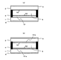
図1は、本発明の第1の実施形態の液晶表示装置の例を示す説明図である。第1の実施形態の液晶表示装置15は、第1の透明基板1と、第2の透明基板2と、第3の透明基板3と、第1の接着材4と、液晶層5と、第2の接着材6と、位相差層7と、第1の偏光板8と、第2の偏光板9とを備える。ここでは、各透明基板1〜3が、それぞれガラス基板である場合を例にして説明するが、各透明基板1〜3は、ガラス基板以外の透明基板であってもよい。以下、各透明基板1〜3をガラス基板1〜3と記す。
[Embodiment 1]
FIG. 1 is an explanatory diagram illustrating an example of a liquid crystal display device according to a first embodiment of the present invention. The liquid
第1のガラス基板1と第2のガラス基板2は、液晶層5を挟持する。具体的には、第1の接着材4が第1のガラス基板1と第2のガラス基板2の外周部分を接着する。そして、第1のガラス基板1、第2のガラス基板2、および第1の接着材4に囲まれた空間に、液晶が充填され、この空間に液晶層5が封止される。第1のガラス基板1と第2のガラス基板2との間に液晶を充填する際には、第1の接着材4に、液晶を注入するための注入口を設け、液晶の充填後、その注入口を塞げばよい。第1の接着材4は、シール材とも呼ばれる。
The
液晶層5を挟持する2枚のガラス基板1,2のうち、視認側とは反対側のガラス基板を第1のガラス基板1とし、視認側のガラス基板を第2のガラス基板2とする。
Of the two
また、本発明の液晶表示装置は、ノーマリブラックのIPSモードの液晶表示装置である。具体的には、液晶層5を挟持する第1のガラス基板1と第2のガラス基板2のうち、いずれか一方のガラス基板には、各画素に共通に配置される共通電極(図1において図示略)と、画素毎に配置される画素電極(図1において図示略)が、液晶層5側に設けられる。
The liquid crystal display device of the present invention is a normally black IPS mode liquid crystal display device. Specifically, either one of the
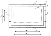
図2は、液晶表示装置15の有効表示領域を示す説明図である。図2では、表示画像の視認側から液晶表示装置15を観察した状態を示している。液晶表示装置15の画素17の集合が有効表示領域16となる。有効表示領域16内の各画素では、共通電極および画素電極によって電界が印加されると、液晶分子の配向方向が変化する。
FIG. 2 is an explanatory diagram showing an effective display area of the liquid
本例では、視認側から観察したとき、液晶表示装置15が矩形となる場合を例にする。また、視認側から観察したとき、各画素は縦方向および横方向にマトリクス状に並び、有効表示領域16も矩形となる場合を例にする。
In this example, a case where the liquid
図3は、1つの画素における共通電極と画素電極の例を示す説明図である。1画素に一つの画素電極22が配置される。一方、共通電極21は、他の画素にも伸び、各画素に共通に配置されている。換言すれば、共通電極21は、各画素に渡って配置されている。また、図3に示すように、画素電極22および共通電極21は、いずれも櫛歯状の形状であり、互いの櫛歯状の突起が噛み合うように配置される。
FIG. 3 is an explanatory diagram illustrating an example of a common electrode and a pixel electrode in one pixel. One
画素電極22には、TFT(Thin Film Transistor)等のアクティブ素子(図示略)を介して、ソースライン(図示略)およびゲートライン(図示略)に接続される。例えば、各画素電極22はマトリクス状に配置される。そして、マトリクス状に配置された画素電極22の行に沿ってゲートラインが配置され、列に沿ってソースラインが配置される。各画素電極22のTFT(図示略)のゲートはゲートラインに接続され、TFTのソースはソースラインに接続され、ドレインは画素電極22に接続される。
The
液晶表示装置が駆動されていないときには、画素電極22と共通電極21との間に電界は印加されない。このとき、液晶層5の液晶分子は、第1のガラス基板1および第2のガラス基板2に対して平行に配向する。このときの配向の向きは、第1のガラス基板1および第2のガラス基板2の液晶層側の面に設けられた配向層(例えば、配向膜。図示略。)によって規定される。例えば、第1のガラス基板1および第2のガラス基板2の配向膜に対して、ラビングを行っておくことにより、液晶分子は、各ガラス基板1,2に平行であって、かつ、ラビング方向に沿うように配向する。第1のガラス基板1および第2のガラス基板2の各配向膜に対しては、その2枚のガラス基板を対向させたときに同じ方向になるように、ラビング処理を行えばよい。この結果、電界が印加されていない状態で、第1のガラス基板1近傍の液晶分子と、第2のガラス基板2近傍の液晶分子は、同じ方向に配向し、また、中間層の液晶分子も、同じ方向に配向する。
When the liquid crystal display device is not driven, no electric field is applied between the
液晶表示装置を駆動する場合、駆動装置(図示略)は、共通電極21を所定の電位に設定する。また、駆動装置は、ゲートラインを線順次選択し、選択したゲートラインをオン電位に設定し、他のゲートラインをオフ電位に設定する。また、駆動装置は、各ソースラインの電極を、選択行の各画素の輝度に応じた電位に設定する。TFTは、ゲートがオン電位に設定されたときに、ソースとドレインとを導通状態にするので、ゲートラインが選択された行の各画素では、各列の画素電極が、自身の列のソースラインと等電位になる。画素電極22および共通電極21は、互いの櫛歯状の突起が噛み合うように配置されている(図3参照)。従って、画素電極22および共通電極21によって、第1のガラス基板1と第2のガラス基板2に対して平行な電界が印加される。すると、液晶層5の液晶分子は、電界が印加されていないときの配向方向から、配向方向を変化させる。具体的には、第1のガラス基板1と第2のガラス基板2に対して平行な面内で配向方向を変化させる。この変化量は、ガラス基板1,2に平行な電界の強さに依る。
When driving the liquid crystal display device, the drive device (not shown) sets the
位相差層7は、第1の透明基板1および第2の透明基板2のうちのいずれか一方の透明基板において、液晶層5とは反対側の面に配置される。図1では、第2のガラス基板2における液晶層5とは反対側の面に位相差層7を配置する場合を例示しているが、第1のガラス基板1における液晶層5とは反対側の面に位相差層7を配置してもよい。位相差層7は、透過光に対して、その透過光の半波長の位相差を生じさせる。
The
この位相差層7の位相差は、液晶層5のリタデーションの50%以上150%以下の範囲内とする。例えば、位相差層7の位相差が液晶層5のリタデーションの50%以上150%以下の範囲内であるという関係を満たすように、液晶層5のリタデーションを規定すればよい。この範囲内に液晶層5のリタデーションを規定することで、ガラス基板の歪による光漏れをより抑制することができる。
The retardation of the
位相差層7として、例えば、1/2波長板を用いることができる。ここでは、位相差層7が1/2波長板である場合を例にして説明する。
For example, a half-wave plate can be used as the
第3のガラス基板3は、第1のガラス基板1と第2のガラス基板2のうち、1/2波長板(位相差層)7が設けられた方のガラス基板(本例では、第2のガラス基板2)に固着される。このとき、第3のガラス基板3は、1/2波長板7を間に介して、その1/2波長板7が配置されたガラス基板(第2のガラス基板2)と対向するように固着される。第3のガラス基板3の厚さに関しては後述する。
The
第3のガラス基板3と第2のガラス基板2は、第2の接着材6によって接着される。この結果、第3のガラス基板3は、1/2波長板7が配置された第2のガラス基板2に固着される。
The
なお、第2の接着材6は、少なくとも、第3のガラス基板3と第2のガラス基板2とを接着する。第3のガラス基板3と第2のガラス基板2は、互いに接着された状態で1/2波長板7を挟み込んで、1/2波長板7を支持してもよい。あるいは、第2の接着材6を用いて、1/2波長板7を、第2のガラス基板2あるいは第3のガラス基板3、またはその両方に接着してもよい。
Note that the
第2の接着材6として、光硬化型の接着材材料を用いることが好ましい。熱硬化型の接着材材料を用いた場合と比較すると、熱硬化型の接着材では接着材を硬化させるための加熱処理で1/2波長板(位相差層)7に影響を与えてしまうおそれがある。一方、光硬化型の接着材では、接着材材料を硬化させるための処理として光照射を行い、加熱処理は行わないので、熱による1/2波長板7への影響を防ぐことができる。熱硬化型の接着材材料の例として、熱硬化型樹脂が挙げられる。第2の接着材6としては、第3のガラス基板3が第1のガラス基板1、第2のガラス基板2の変形に追従するように、変形応力を緩和しない硬い材料(すなわち、ヤング率の高い材料)が好ましい。例えば、ヤング率が100MPa以上の材料が好ましい。
As the
また、第2の接着材6として、第1の接着材4と同一材料の接着材材料を用いることが好ましい。この場合、接着材として複数種類の接着材材料を用意する必要がない。従って、液晶表示装置15の製造工程を効率化することができる。
Moreover, it is preferable to use the same adhesive material as the
第1のガラス基板1と第2のガラス基板2のうち、1/2波長板7が設けられていない方のガラス基板(本例では、第1のガラス基板1)には、液晶層5とは反対側の面に第1の偏光板8が設けられる。
Of the
また、第3のガラス基板3は、1/2波長板7とは反対側の面に第2の偏光板9を備える。第2の偏光板9は、第2の偏光板9自身の吸収軸が第1の偏光板8の吸収軸と直交するように配置される。
The
なお、図1に例示するように、第3のガラス基板3と第2の偏光板9との間に、透明な導電層10を配置することが好ましい。透明な導電層10を配置することにより、第3のガラス基板3と第2の偏光板9との間の帯電を防ぎ、帯電による表示不良を防止することができる。また、液晶層5を駆動する電極が帯電することを防止することができる。なお、この透明導電層10に所定の電位、例えば、接地電位や液晶駆動電位の1/2の電位を与えることが好ましい。
As illustrated in FIG. 1, it is preferable to dispose a transparent
次に、画素電極22および共通電極21によって電界が印加されていないときの液晶層5の液晶分子の配向方向(以下、電界非印加時配向方向と記す。)、位相差層(本例では1/2波長板7)の遅相軸、および各偏光板8,9の吸収軸の関係について説明する。図4は、電界非印加時配向方向、位相差層7の遅相軸、各偏光板8,9の吸収軸の関係の例を示す説明図である。図4では、第1の偏光板8、第1のガラス基板1、液晶層5、第2のガラス基板2、1/2波長板7、第3のガラス基板3、および第2の偏光板9を視認側から観察した場合の状態を模式的に示している。また、図4において、偏光板8,9に図示した矢印は吸収軸を表し、液晶層5に図示した矢印は、電界非印加時配向方向を表し、1/2波長板7に図示した矢印は、遅相軸を表している。
Next, the alignment direction of the liquid crystal molecules of the
既に説明したように、第1の偏光板8の吸収軸と第2の偏光板9の吸収軸とは直交する(図4参照)。
As already described, the absorption axis of the first
また、光漏れを抑えるという効果を向上させるために、1/2波長板7の遅相軸が電界非印加時配向方向と直交するか、または、平行になるようにすることが好ましい。図4では、1/2波長板7の遅相軸が電界非印加時配向方向と直交する場合を例示している。このように、1/2波長板7の遅相軸が電界非印加時配向方向と直交するように1/2波長板7を配置することがさらに好ましい。1/2波長板7の遅相軸と電界非印加時配向方向とが直交する場合には、遅相軸と電界非印加時配向方向とが平行である場合に比べて、波長分散による着色を抑えることができる。ただし、遅相軸と電界非印加時配向方向とを平行とする構成であっても、電界が印加されていない時に応力が加えられた場合の光漏れを抑えることができる。
In order to improve the effect of suppressing light leakage, it is preferable that the slow axis of the half-
さらに、1/2波長板7の遅相軸が第2の偏光板9の吸収軸と平行であり、電界非印加時配向方向が第1の偏光板8の吸収軸と平行であるという条件を満たしていることが好ましい。図4では、この条件を満たす場合を満たしている。すなわち、1/2波長板7の遅相軸が第2の偏光板9の吸収軸と平行となり、電界非印加時配向方向が第1の偏光板8の吸収軸と平行となるように、第1の偏光板8および第2の偏光板9を配置する場合を示している。上記の条件を満たす場合にも、波長分散による着色を抑えることができる。ただし、上記の条件を満たしていなくてもよい。ただし、少なくとも第1の偏光板8および第2の偏光板9の吸収軸に関しては、互いに直交させる。
Furthermore, the slow axis of the half-
図4に示す例では、1/2波長板7の遅相軸が電界非印加時配向方向と直交するように1/2波長板7を配置し、第1の偏光板8の吸収軸が電界非印加時配向方向と平行になるように第1の偏光板8を配置し、第2の偏光板9の吸収軸が1/2波長板7の遅相軸と平行になるように第2の偏光板9を配置した場合を示している。この場合、2枚の偏光板8,9の吸収軸は直交する。
In the example shown in FIG. 4, the half-
上記のように、1/2波長板7の遅相軸が第2の偏光板9の吸収軸と平行であり、電界非印加時配向方向が第1の偏光板8の吸収軸と平行であるという条件は満たされていなくてもよい。また、遅相軸と電界非印加時配向方向とが平行になっていてもよい。従って、電界非印加時配向方向、遅相軸および吸収軸の関係は、図4の場合に限定されない。図5は、電界非印加時配向方向、遅相軸および吸収軸の関係の他の例を示す説明図である。
As described above, the slow axis of the half-
図5(a)に示す例では、1/2波長板7の遅相軸が電界非印加時配向方向と平行になるように1/2波長板7を配置する。そして、第1の偏光板8の吸収軸が電界非印加時配向方向と平行になるように第1の偏光板8を配置する。また、第2の偏光板9の吸収軸が1/2波長板7の遅相軸と直交するように第2の偏光板9を配置する。
In the example shown in FIG. 5A, the half-
また、図5(b)に示す例では、1/2波長板7の遅相軸が電界非印加時配向方向と平行になるように1/2波長板7を配置する。そして、第1の偏光板8の吸収軸が電界非印加時配向方向と直交するように第1の偏光板8を配置する。また、第2の偏光板9の吸収軸が1/2波長板7の遅相軸と平行になるように第2の偏光板9を配置する。
In the example shown in FIG. 5B, the half-
また、図5(c)に示す例では、1/2波長板7の遅相軸が電界非印加時配向方向と直交するように1/2波長板7を配置する。そして、第1の偏光板8の吸収軸が電界非印加時配向方向と直交するように第1の偏光板8を配置する。また、第2の偏光板9の吸収軸が1/2波長板7の遅相軸と直交するように第2の偏光板9を配置する。
In the example shown in FIG. 5C, the half-
電界非印加時配向方向、遅相軸および吸収軸の関係が図5(a)〜(c)に例示する関係である場合であっても、第1の偏光板8および第2の偏光板9の吸収軸は互いに直交する。また、1/2波長板7の遅相軸と電界非印加時配向方向とが直交または平行となっている。
Even when the relationship between the orientation direction when no electric field is applied, the slow axis, and the absorption axis is the relationship illustrated in FIGS. 5A to 5C, the first
次に、第1の偏光板8側から入射した光の偏光状態の変化について説明する。図6は、液晶表示装置内を通過する光の偏光状態の変化を示す説明図である。図6では、電界非印加時配向方向、遅相軸および各吸収軸が図4と同様の関係になる場合を示している。また、液晶表示装置は駆動されておらず、共通電極21と各画素電極22の間に電界が生じていないものとする。そして、その状態で、液晶表示装置を曲げる力が加えられ、第1の偏光板8の吸収軸を基準に45°ずれた方向に応力が発生しているものとする。第1のガラス基板1および第3のガラス基板3に示した矢印は、それぞれ応力の方向を示している。本例では、第3のガラス基板3には、第3のガラス基板3を伸ばそうとする応力が発生し、第1のガラス基板1には、第1のガラス基板1を縮めようとする応力が発生する場合を示す。
Next, a change in the polarization state of light incident from the first
また、第1のガラス基板1と第2のガラス基板2は第1の接着材4により接着され、第2のガラス基板2と第3のガラス基板3は第2の接着材6により接着されている。従って、液晶表示装置を合板と考えることができる。そして、中立面は、第2のガラス基板2に存在するので、第2のガラス基板2には応力は生じていない。厳密には、第2のガラス基板2の中立面の上側と下側とで逆向きの応力が生じるが、両者が相殺しあい、第2のガラス基板2には応力は生じていないとみなすことができる。
The
第1の偏光板8に、種々の方向に直線偏光している光が入射したとする。この光が第1の偏光板8を通過したとき、光の偏光状態は、第1の偏光板8の吸収軸に直交する方向の直線偏光となる(図6参照)。
Assume that light linearly polarized in various directions is incident on the first
応力により光弾性効果の生じた第1のガラス基板1は、1軸位相差板としての機能を持つことになる。そして、第1のガラス基板1における遅相軸は、応力の方向と同じである。従って、第1の偏光板8を通過した直線偏光の光が、その偏光方向と45°をなす方向に応力が生じている第1のガラス基板1を通過すると、楕円偏光の光になる(図6参照)。
The
さらに、この楕円偏光の光が、電界非印加時配向方向に配向した液晶層5を通過すると、回転が逆向きの楕円偏光の光となる(図6参照)。
Further, when this elliptically polarized light passes through the
次に、この光は、第2のガラス基板2を通過する。第2のガラス基板2には応力が生じていない。従って、第2のガラス基板2の通過前後で偏光状態は変化せず、液晶層5を通過したときと同じ向きの回転の楕円偏光となっている。
Next, this light passes through the
次に、この楕円偏光の光は、1/2波長板7を通過する。1/2波長板7は、1/2波長板7自身を通過する楕円偏光の光の偏光状態を次のように変化させる。すなわち、楕円偏光の長軸が、1/2波長板7の遅相軸を中心に線対称に反転するように変化させ、また、楕円偏光の向きを逆回転に変化させる。従って、1/2波長板7を通過した光の楕円偏光の回転の向きは、第2のガラス基板2を通過したときとは逆向きになっている。すなわち、1/2波長板7を通過した光の楕円偏光の回転の向きは、第1のガラス基板1を通過したときの楕円偏光の回転の向きと同じである。
Next, the elliptically polarized light passes through the half-
第3のガラス基板3には、第1の偏光板8の吸収軸に対して45°ずれた方向に応力が生じている。従って、上記の1/2波長板7を通過した楕円偏光の光が第3のガラス基板3を通過すると、光の偏光状態は、第1のガラス基板1を通過する前と同様の直線偏光となる。
The
この直線偏光の方向は、第2の偏光板9の吸収軸と平行である。従って、第3のガラス基板3を通過した光は、第2の偏光板9を通過しない。
The direction of this linearly polarized light is parallel to the absorption axis of the second
従って、液晶層5に電界が印加されずに有効表示領域全体が黒色表示となる状態で光漏れを抑えることができる。すなわち、ノーマリブラックの液晶表示装置15において、電界が印加されていない時に応力が加えられた場合の光漏れを抑えることができる。また、このとき、1/2波長板7の位相が液晶層5のリタデーションの50%以上150%以下であることにより、光漏れを抑える効果をより高めることができる。
Accordingly, light leakage can be suppressed in a state where the entire effective display area is displayed in black without applying an electric field to the
次に、第3のガラス基板8の厚さについて説明する。ここでは、第1のガラス基板1と第2のガラス基板2とで、厚さ、ヤング率および光弾性係数がそれぞれ共通であるものとする。そして、第1のガラス基板1および第2のガラス基板2の厚さをd1とする。第1のガラス基板1および第2のガラス基板2のヤング率をE1とする。第1のガラス基板1および第2のガラス基板2の光弾性係数をC1とする。また、第3のガラス基板3の厚さをd3とする。第3のガラス基板3のヤング率をE3とする。第3のガラス基板3の光弾性係数をC3とする。
Next, the thickness of the
図7は、第1のガラス基板における視認側とは反対側の面の高さを0としたときの、ガラス基板間の境界の高さを示す説明図である。第1のガラス基板における視認側とは反対側の面(以下、底面と記す。)からの高さを変数yで表すものとする。 FIG. 7 is an explanatory diagram showing the height of the boundary between the glass substrates when the height of the surface of the first glass substrate opposite to the viewing side is zero. The height from the surface of the first glass substrate opposite to the viewing side (hereinafter referred to as the bottom surface) is represented by a variable y.
第1から第3までの各ガラス基板1,2,3の厚さは、各偏光板8,9の厚さ、液晶層5の厚さ、第2および第3のガラス基板間の間隔に比べて非常に大きく、各偏光板8,9の厚さ、液晶層5の厚さ、第2および第3のガラス基板間の間隔は、無視できる。従って、第1のガラス基板1と第2のガラス基板2との境界の高さはd1である。また、第2のガラス基板2と第3のガラス基板3との境界の高さは2d1である。また、第3のガラス基板3の視認側の面の高さは2d1+d3である。また、この高さ2d1+d3をdとする。
The thicknesses of the first to
また、第1から第3までの各ガラス基板1,2,3における位相差をそれぞれ、δ1,δ2,δ3とする。このとき、以下の式(4)の光学補償条件が成立していれば、第1から第3までの各ガラス基板1,2,3における位相差がキャンセルされる。
In addition, the phase differences in the first to third glass substrates 1 , 2 , and 3 are set as δ 1 , δ 2 , and δ 3 , respectively. At this time, if the optical compensation condition of the following expression (4) is satisfied, the phase differences in the first to
δ1−δ2+δ3=0 式(4) δ 1 −δ 2 + δ 3 = 0 Formula (4)
なお、式(4)において、δ2に関して減算となっているのは、第2のガラス基板2により光の楕円偏光の方向が逆向きになるからである。また、光弾性効果で発生する位相差は、既述の式(3)で表される。
In Equation (4), δ 2 is subtracted because the
従って、式(4)の両辺に、λ/(2π)を乗じると、光学補償条件は以下の式(5)で表すことができる。λは、光の波長である。 Therefore, when both sides of the equation (4) are multiplied by λ / (2π), the optical compensation condition can be expressed by the following equation (5). λ is the wavelength of light.
C1σ1d1−C1σ2d1+C3σ3d3=0 式(5) C 1 σ 1 d 1 −C 1 σ 2 d 1 + C 3 σ 3 d 3 = 0 Equation (5)
式(5)において、σ1は第1のガラス基板1の応力である。σ2は第2のガラス基板2の応力である。σ3は第3のガラス基板3の応力である。
In Expression (5), σ 1 is the stress of the
ここで、3枚のガラス基板1〜3のうちの任意のガラス基板iに関して、以下の式(6)が成り立つ。
Here, with respect to an arbitrary glass substrate i among the three
σi=(σi上面+σi下面)/2 式(6) σ i = (σ i upper surface + σ i lower surface ) / 2 Formula (6)
σi上面は、ガラス基板iの上面における応力である。σi下面は、ガラス基板iの下面における応力である。また、応力によって液晶表示装置に曲げが生じたときの曲率半径をρとする。また、中立面の高さをDとする。 The σ i upper surface is a stress on the upper surface of the glass substrate i. The σ i lower surface is a stress on the lower surface of the glass substrate i. Further, the curvature radius when the liquid crystal display device is bent due to the stress is represented by ρ. Further, the height of the neutral plane is D.
このとき、第3のガラス基板3に関しては、以下の式(7)、式(8)が成立する。
At this time, with respect to the
σ3上面=E3(2d1+d3−D)/ρ 式(7)
σ3下面=E3(2d1−D)/ρ 式(8)
σ 3 upper surface = E 3 (2d 1 + d 3 −D) / ρ Equation (7)
σ 3 lower surface = E 3 (2d 1 −D) / ρ Equation (8)
よって、第3のガラス基板3におけるσ3は以下の式(9)によって表される。
Therefore, sigma 3 in the
σ3=E3(4d1+d3−2D)/2ρ 式(9) σ 3 = E 3 (4d 1 + d 3 −2D) / 2ρ Equation (9)
また、第2のガラス基板2に関しては、以下の式(10)、式(11)が成立する。
Further, for the
σ2上面=E1(2d1−D)/ρ 式(10)
σ2下面=E1(d1−D)/ρ 式(11)
σ 2 upper surface = E 1 (2d 1 −D) / ρ Equation (10)
σ 2 lower surface = E 1 (d 1 −D) / ρ Equation (11)
よって、第2のガラス基板2におけるσ2は以下の式(12)によって表される。
Thus, 2 sigma of the
σ2=E1(3d1−2D)/2ρ 式(12) σ 2 = E 1 (3d 1 −2D) / 2ρ Formula (12)
また、第1のガラス基板1に関しては、以下の式(13)、式(14)が成立する。
Further, for the
σ1上面=E1(d1−D)/ρ 式(13)
σ1下面=E1(−D)/ρ 式(14)
σ 1 upper surface = E 1 (d 1 −D) / ρ Equation (13)
σ 1 lower surface = E 1 (−D) / ρ Formula (14)
よって、第1のガラス基板1におけるσ1は以下の式(15)によって表される。
Therefore, sigma 1 in the
σ1=E1(d1−2D)/2ρ 式(15) σ 1 = E 1 (d 1 −2D) / 2ρ Equation (15)
また、中立面の高さDは、式(1)で表される。ただし、各ガラス基板1〜3の幅は等しく、液晶表示装置に曲げが生じても、基板1〜3の幅は等しい状態が保たれているものとする。すなわち、式(1)におけるb(y)は一定であるものとする。このとき、中立面の高さDは、以下の式(16)で表される。
Further, the height D of the neutral surface is expressed by the formula (1). However, the widths of the
式(5)に、式(9)、式(12)、式(15)および式(16)を代入し、d3に関して解くと、d3は、以下の式(17)で表される。 In equation (5), equation (9), by substituting Equation (12), equation (15) and (16), when solving for d 3, d 3 is expressed by the following equation (17).
すなわち、第3のガラス基板3の厚さd3が式(17)を満たしていれば、各ガラス基板1,2,3における位相差がキャンセルし、光漏れを防止することができる。
That is, if the thickness d3 of the third
ただし、第3のガラス基板3の厚さd3が式(17)を満足していなくてもよい。d3が式(17)を満足していなくても、第3のガラス基板3および1/2波長板7を設けない場合に比べて、光漏れを抑えることができる。以下、第3のガラス基板3および1/2波長板7を設けない場合に比べて、光漏れを抑えることができるd3の条件を説明する。
However, the thickness d3 of the third
第3のガラス基板3および1/2波長板7を設けずに、第2のガラス基板2上に第2の偏光板9を配置する一般的な構成に比べて、光漏れが減少するためには、以下の条件が成立していればよい。すなわち、第3のガラス基板3および1/2波長板7を設けない構成としたときの第1のガラス基板1および第2のガラス基板2における位相差よりも、第3のガラス基板3および1/2波長板7を設けた構成としたときの第1から第3までの各ガラス基板における位相差の方が小さければよい。具体的には、第3のガラス基板3および1/2波長板7を設けない構成としたときの第1のガラス基板1、第2のガラス基板2の位相差をそれぞれδ1’,δ2’とすると、以下の式(18)が成立していればよい。
Compared with a general configuration in which the second
δ1−δ2+δ3<|δ1’−δ2’| 式(18) δ 1 −δ 2 + δ 3 <| δ 1 ′ −δ 2 ′ | Formula (18)
光弾性効果で発生する位相差は、既述の式(3)で表されるので、式(4)を式(5)に変形した場合と同様に、式(18)の両辺にλ/(2π)を乗じると、以下の式(19)で表すことができる。 Since the phase difference generated by the photoelastic effect is expressed by the above-described equation (3), λ / () is added to both sides of the equation (18) as in the case where the equation (4) is transformed into the equation (5). When 2π) is multiplied, it can be expressed by the following equation (19).
C1σ1d1−C1σ2d1+C3σ3d3<|C1σ1’d1−C1σ2’d1|
式(19)
C 1 σ 1 d 1 -C 1 σ 2 d 1 + C 3 σ 3 d 3 <| C 1 σ 1 'd 1 -C 1 σ 2 ' d 1 |
Formula (19)
式(19)において、σ1’は、第3のガラス基板3および1/2波長板7を設けない構成としたときの第1のガラス基板1の応力である。σ2’は、第3のガラス基板3および1/2波長板7を設けない構成としたときの第2のガラス基板2の応力である。この構成の場合における2枚のガラス基板のうち個々のガラス基板iに関しても既述の式(6)が成り立つ。
In Expression (19), σ 1 ′ is the stress of the
また、第3のガラス基板3および1/2波長板7を設けない構成としたときの中立面の高さをD’とすると、第2のガラス基板2に関して、以下の式(20)、式(21)が成り立つ。
Further, assuming that the height of the neutral surface when the
σ2上面’=E1(2d1−D’)/ρ 式(20)
σ2下面’=E1(d1−D’)/ρ 式(21)
σ 2 upper surface ′ = E 1 (2d 1 −D ′) / ρ Formula (20)
σ 2 lower surface ′ = E 1 (d 1 −D ′) / ρ Formula (21)
よって、式(6)により、σ2’は以下の式(22)によって表される。 Therefore, σ 2 ′ is expressed by the following equation (22) according to equation (6).
σ2’=E1(3d1−2D’)/2ρ 式(22) σ 2 ′ = E 1 (3d 1 −2D ′) / 2ρ Equation (22)
同様に、第3のガラス基板3および1/2波長板7を設けない構成としたとき、第1のガラス基板1に関して、以下の式(23)、式(24)が成り立つ。
Similarly, when the
σ1上面’=E1(d1−D’)/ρ 式(23)
σ1下面’=E1(−D’)/ρ 式(24)
σ 1 upper surface ′ = E 1 (d 1 −D ′) / ρ Equation (23)
σ 1 lower surface ′ = E 1 (−D ′) / ρ Formula (24)
よって、σ1’は以下の式(25)によって表される。 Therefore, σ 1 ′ is expressed by the following equation (25).
σ1’=E1(d1−2D’)/2ρ 式(25) σ 1 ′ = E 1 (d 1 −2D ′) / 2ρ Equation (25)
また、第3のガラス基板3および1/2波長板7を設けない構成としたときの中立面の高さD’は、以下の式(26)で表される。ただし、式(1)におけるb(y)は一定であるものとする。
Further, the height D ′ of the neutral plane when the
式(7)に、式(9)、式(12)、式(15)、式(22)、式(25)および式(26)を代入し、d3に関して解くと、以下の式(27)で表される。 Substituting Equation (9), Equation (12), Equation (15), Equation (22), Equation (25), and Equation (26) into Equation (7) and solving for d 3 yields the following equation (27) ).
すなわち、第3のガラス基板3の厚さd3が式(27)を満たしていれば、第3のガラス基板3および1/2波長板7を設けない一般的な構成に比べて、光漏れを減少することができる。そして、特に光漏れを抑えることができるのは、d3が前述の式(17)を満たしている場合である。
That is, as long as the thickness d 3 of the
次に、1/2波長板(位相差層)7および第2の接着材6の配置について説明する。図8は、1/2波長板7および第2の接着材6の配置例を示す説明図である。図8に示すように、1/2波長板7の配置領域は、有効表示領域16よりも大きく、有効表示領域16を包含することが好ましい。すなわち、1/2波長板7は、有効表示領域16よりも大きな面積となるように形成し、有効表示領域16を内部に含むように配置すればよい。あるいは、1/2波長板7の配置領域は有効表示領域16と一致してもよい。すなわち、1/2波長板7を有効表示領域16と同一面積かつ同一形状となるように形成し、有効表示領域16と一致するように重ねて配置してもよい。いずれの場合であっても、有効表示領域16上に1/2波長板7が存在することになるので、有効表示領域16全体に渡って光漏れを抑えることができる。
Next, the arrangement of the half-wave plate (retardation layer) 7 and the
また、第2の接着材6は、少なくとも有効表示領域16の各辺の外側の領域に配置する。また、このとき、有効表示領域16の個々の辺の外側の領域で、個々の辺に沿って配置される第2の接着材6の長さは、その配置位置に対応する有効表示領域16の辺の長さの1/2以上とすることが好ましい。図8に示す例では、有効表示領域16の外側において、有効表示領域16の各辺に沿って4箇所に第2の接着材6が配置されている。有効表示領域16の長辺の近傍では、その長辺の長さをwa1とし、その長辺に沿って配置される第2の接着材6の長さをwa2とすると(図8参照)、wa2≧wa1/2を満足するように、第2の接着材6を配置することが好ましい。同様に、有効表示領域16の短辺近傍では、その短辺の長さをwb1とし、その短辺に沿って配置される第2の接着材6の長さをwb2とすると、wb2≧wb1/2を満足するように、第2の接着材6を配置することが好ましい。このように第2の接着材6を配置することによって、第3のガラス基板3を第2のガラス基板2に確実に固着させることができる。その結果、液晶表示装置に曲げ応力が生じたときに、第2のガラス基板2において、第1のガラス基板1側の応力と、第3のガラス基板3側の応力をキャンセルすることができる。
Further, the
また、第2のガラス基板2および第3のガラス基板3の外周部分を全て第2の接着材6で接着せずに、空気の通過口となる部分を空けておいてもよい。そのようにすることによって、第2の接着材6に生じる気泡や貫通孔を防止して、第2のガラス基板2と第3のガラス基板3との接着力を向上させることができる。
Alternatively, the outer peripheral portions of the
また、図8では、有効表示領域16の外側の4箇所に第2の接着材を配置する場合を例示したが、第2の接着材6は、有効表示領域16を全面的に覆うように配置されてもよい。図9は、図8に示す第2の接着材6の配置領域を広げて有効表示領域16を覆うようにした例を示す説明図である。図9に示すように、有効表示領域16を覆うように第2の接着材6を配置する場合、第2の接着材6として透明な接着材材料(例えば、透明樹脂)を用いる。後述するように、第3のガラス基板3は、少なくとも一方の基板面に透明電極を有した静電容量タイプのタッチパネルとしての機能を有していてもよい。この場合、上記の例のように、有効表示領域16を覆うように透明樹脂を配置することにより、タッチパネルで用いる透明樹脂材料や生産設備を液晶表示装置の製造に利用できる。
8 illustrates the case where the second adhesive material is disposed at four locations outside the
また、有効表示領域16を覆うように第2の接着材6を配置する場合、1/2波長板7もガラス基板(ここでは、第2のガラス基板2とする。)に接着される。この場合、1/2波長板7は第2のガラス基板2に接着されるので、2枚のガラス基板間で挟み込んで支持しなくてもよい。すなわち、1/2波長板7が配置されるガラス基板と第3のガラス基板との間の間隔は、1/2波長板7の厚さよりも大きくてもよい。図10は、この場合の例を示す説明図である。図10に示す例では、1/2波長板7は、第2の接着材6によって第2のガラス基板2に接着されている。なお、1/2波長板7と重なる領域では、第2の接着材6が薄く塗布された場合を図示している。また、1/2波長板7の外側に配置された第2の接着材6によって、第2のガラス基板2および第3のガラス基板3の間隔は、h1に規定されているものとする。1/2波長板7の厚さをh2とした場合、h1>h2であってもよい。この場合、図10に示すように、ガラス基板2,3間に空間19が形成される。なお、空間19に第2の接着材6が配置されていてもよい。
When the
また、図1に示すように、1/2波長板7が配置されるガラス基板と第3のガラス基板との間の間隔が、1/2波長板7の厚さと等しくてもよい。
In addition, as shown in FIG. 1, the distance between the glass substrate on which the half-
以上の説明では、第2のガラス基板2に位相差層を設ける場合を説明したが、第1のガラス基板1における液晶層5とは反対側の面に位相差層7を配置してもよい。この場合の構成例を、図11に示す。図1に示す構成要素と同一の構成要素に関しては、図1と同一の符号を付し、詳細な説明を省略する。
In the above description, the case where the retardation layer is provided on the
第1のガラス基板1、第2のガラス基板2、第1の接着材4、液晶層5、共通電極21および各画素電極22に関しては、第2のガラス基板2に1/2波長板(位相差層)7を設ける場合の構成と同様であり、説明を省略する。また、位相差層7の位相差と液晶層5のリタデーションとの関係も既に説明した通りである。
Regarding the
図11に示す構成では、第1のガラス基板1に1/2波長板7を設ける。そして、第3のガラス基板3は、1/2波長板7が設けられた第1のガラス基板1に固着される。このとき、第3のガラス基板3は、1/2波長板7を間に介して、第1のガラス基板1と対向するように固着される。具体的には、第2の接着材6によって、第3のガラス基板3は第1のガラス基板1に接着される。
In the configuration shown in FIG. 11, the half-
図11に示す例では、ガラス基板1,2のうち、第2のガラス基板2が、1/2波長板7が設けられていない方のガラス基板に該当する。この第2のガラス基板2において、液晶層5とは反対側の面に第1の偏光板8が設けられる。
In the example shown in FIG. 11, among the
また、第3のガラス基板3は、1/2波長板7とは反対側の面に第2の偏光板9を備える。この点は、図1に示す構成と同様である。ただし、図11に示す構成では、視認側の偏光板が第1の偏光板8であり、背面側の偏光板が第2の偏光板9である。また、図1に示す場合と同様に、第3のガラス基板3と第2の偏光板9との間に、透明な導電層10を配置することが好ましい。
The
また、1/2波長板、第2の接着材の配置領域の態様や、第3のガラス基板3の好ましい厚さに関しても、既に説明したとおりであり、説明を省略する。
The aspect of the arrangement region of the half-wave plate and the second adhesive and the preferable thickness of the
次に、1/2波長板7を第1のガラス基板11に配置する構成における電界非印加時配向方向、1/2波長板7の遅相軸、各偏光板8,9の吸収軸の関係について説明する。この関係は既に説明したとおりであるが、図11に示す構成に合わせて説明する。図12(a)〜(d)は、それぞれ、電界非印加時配向方向、位相差層7の遅相軸、各偏光板8,9の吸収軸の関係の例を示す説明図である。
Next, the relationship between the orientation direction when no electric field is applied, the slow axis of the half-
図12では、第2の偏光板9、第3のガラス基板3、1/2波長板7、第1のガラス基板1、液晶層5、第2のガラス基板2および第1の偏光板8を視認側から観察した場合の状態を模式的に示している。また、図12に示す各矢印は、図4や図5と同様に、吸収軸、電界非印加時配向方向、遅相軸を表している。
In FIG. 12, the second
第1の偏光板8の吸収軸と第2の偏光板9の吸収軸とは直交させる。
The absorption axis of the first
また、光漏れを抑えるという効果を向上させるために、1/2波長板7の遅相軸が電界非印加時配向方向と直交するか、または、平行になるようにすることが好ましく、特に、遅相軸が電界非印加時配向方向と直交することが好ましい。直交とすることにより、波長分散による着色を抑えることができる。
In order to improve the effect of suppressing light leakage, it is preferable that the slow axis of the half-
さらに、1/2波長板7の遅相軸が第2の偏光板9の吸収軸と平行であり、電界非印加時配向方向が第1の偏光板8の吸収軸と平行であるという条件を満たしていることが好ましい。この場合にも、波長分散による着色を抑えることができる。
Furthermore, the slow axis of the half-
図12(a)に示す例では、1/2波長板7の遅相軸が電界非印加時配向方向と直交するように1/2波長板7を配置し、第1の偏光板8の吸収軸が電界非印加時配向方向と平行になるように第1の偏光板8を配置し、第2の偏光板9の吸収軸が1/2波長板7の遅相軸と平行になるように第2の偏光板9を配置した場合を示している。この場合、2枚の偏光板8,9の吸収軸は直交する。図12(a)に示すように各要素を配置することが特に好ましい。
In the example shown in FIG. 12A, the half-
1/2波長板7の遅相軸が第2の偏光板9の吸収軸と平行であり、電界非印加時配向方向が第1の偏光板8の吸収軸と平行であるという条件が満たされていることが好ましいが、この条件は満たされていなくてもよい。また、遅相軸と電界非印加時配向方向とが平行になっていてもよい。図12(b)〜(c)では、これらの場合の例を示している。
The condition that the slow axis of the half-
図12(b)に示す例では、1/2波長板7の遅相軸が電界非印加時配向方向と平行になるように1/2波長板7を配置する。そして、第1の偏光板8の吸収軸が電界非印加時配向方向と直交するように配置する。また、第2の偏光板9の吸収軸が1/2波長板7の遅相軸と平行になるように第2の偏光板9を配置する。
In the example shown in FIG. 12B, the half-
また、図12(c)に示す例では、1/2波長板7の遅相軸が電界非印加時配向方向と平行になるように1/2波長板7を配置する。そして、第1の偏光板8の吸収軸が電界非印加時配向方向と平行になるように第1の偏光板8を配置する。また、第2の偏光板9の吸収軸が1/2波長板7の遅相軸と直交するように第2の偏光板9を配置する。
In the example shown in FIG. 12C, the half-
図12(d)に示す例では、1/2波長板7の遅相軸が電界非印加時配向方向と直交するように1/2波長板7を配置する。そして、第1の偏光板8の吸収軸が電界非印加時配向方向と直交するように第1の偏光板8を配置する。また、第2の偏光板9の吸収軸が1/2波長板7の遅相軸と直交するように第2の偏光板9を配置する。
In the example shown in FIG. 12D, the half-
電界非印加時配向方向、遅相軸および吸収軸の関係が図12(b)〜(d)に例示する関係である場合であっても、第1の偏光板8および第2の偏光板9の吸収軸は互いに直交する。また、1/2波長板7の遅相軸と電界非印加時配向方向とが直交または平行となっている。
Even when the relationship between the orientation direction when no electric field is applied, the slow axis, and the absorption axis is the relationship illustrated in FIGS. 12B to 12D, the first
また、液晶表示装置を通過する光の偏光状態の変化は、図6に示す場合と同様であるが、図11に示す構成に合わせて説明する。図13は、液晶表示装置内を通過する光の偏光状態の変化を示す説明図である。図13では、電界非印加時配向方向、遅相軸および各吸収軸が図12(a)と同様の関係になる場合を示している。また、液晶表示装置は駆動されておらず、共通電極21と各画素電極22の間に電界が生じていないものとする。そして、液晶表示装置において、第2の偏光板9の吸収軸を基準に45°ずれた方向に応力が発生しているものとする。
The change in the polarization state of the light passing through the liquid crystal display device is the same as that shown in FIG. 6, but will be described according to the configuration shown in FIG. FIG. 13 is an explanatory diagram showing changes in the polarization state of light passing through the liquid crystal display device. FIG. 13 shows a case where the orientation direction when no electric field is applied, the slow axis, and each absorption axis have the same relationship as in FIG. Further, it is assumed that the liquid crystal display device is not driven and no electric field is generated between the
第2の偏光板9に、種々の方向に直線偏光している光が入射したとする。この光が第2の偏光板9を通過すると、光の偏光状態は、第2の偏光板9の吸収軸に直交する方向の直線偏光となる。
It is assumed that light that is linearly polarized in various directions is incident on the second
この直線偏光の光が、その偏光方向と45°をなす方向に応力が生じている第3のガラス基板3を通過すると、楕円偏光の光になる。
When the linearly polarized light passes through the
さらに、この楕円偏光の光が、1/2波長板7を通過すると、回転が逆向きの楕円偏光の光となる。
Further, when this elliptically polarized light passes through the half-
次に、この光は、第1のガラス基板1を通過する。第1のガラス基板1には応力が生じていない。従って、第1のガラス基板1の通過前後で偏光状態は変化せず、1/2波長板7を通過したときと同じ向きの回転の楕円偏光となっている。
Next, this light passes through the
次に、この楕円偏光の光は、液晶層5を通過する。液晶層5を通過した光の楕円偏光の向きは、第1のガラス基板1を通過したときとは逆向きになっている。すなわち、液晶層5を通過した光の偏光状態は、第3のガラス基板3を通過したときと同じになっている。
Next, the elliptically polarized light passes through the
この光が、第2のガラス基板2を通過すると、光の偏光状態は、第3のガラス基板3を通過する前と同様の直線偏光となる。
When this light passes through the
この直線偏光の方向は、第1の偏光板8の吸収軸と平行である。従って、第2のガラス基板2を通過した光は、第1の偏光板8を通過しない。
The direction of this linearly polarized light is parallel to the absorption axis of the first
従って、ノーマリブラックの液晶表示装置15において、電界が印加されていない時に応力が加えられた場合の光漏れを抑えることができる。
Therefore, in the normally black liquid
なお、本発明において、液晶表示装置を駆動して、有効表示領域に画像を表示している状態では、応力が生じても表示品位に影響しないので、問題は生じない。 In the present invention, when the liquid crystal display device is driven and an image is displayed in the effective display area, no problem occurs because the display quality is not affected even if stress occurs.
[実施形態2]
第2の実施形態および第3の実施形態では、液晶層に電界が印加されずに有効表示領域全体が黒色表示となる状態で光漏れを抑えることができるという効果とともに、その黒色表示時における視野角を拡大することができる液晶表示装置を示す。
[Embodiment 2]
In the second embodiment and the third embodiment, the field of view at the time of black display is provided, together with the effect that light leakage can be suppressed in a state where the entire effective display area becomes black display without applying an electric field to the liquid crystal layer. 1 shows a liquid crystal display device capable of enlarging a corner.
図14は、本発明の第2の実施形態の液晶表示装置の例を示す説明図である。第1の実施形態と同様の構成要素については、図1と同一の符号を付し、説明を省略する。 FIG. 14 is an explanatory diagram illustrating an example of the liquid crystal display device according to the second embodiment of the present invention. The same components as those in the first embodiment are denoted by the same reference numerals as those in FIG.
第2の実施形態の液晶表示装置は、第1の偏光板8と第2の偏光板9のいずれか一方の偏光板と、その偏光板に最も近接するガラス基板との間に二軸性位相差板(biaxial film)31を備える。すなわち、第3の透明基板3と第2の偏光板9との間、または、第1の透明基板1と第1の偏光板8との間に二軸性位相差板31を備える。図14では、第3の透明基板3と第2の偏光板9との間に二軸性位相差板31を備える構成を例示しているが、二軸性位相差板31は、第1のガラス基板1と第二の偏光板8との間に配置されてもよい。
The liquid crystal display device according to the second embodiment has a biaxial position between any one of the first
二軸性位相差板31は、面内の一方向に加え、厚み方向にも位相差を持つ位相差板であり、Nz板とも称される。
The
二軸性位相差板31における遅相軸方向の屈折率をnxとし、二軸性位相差板31における主面に平行でその遅相軸に直交する方向の屈折率をnyとする。また、二軸性位相差板31の厚さ方向の屈折率をnzとする。二軸性位相差板31は、nx>nz>nyという条件を満足する。
The refractive index in the slow axis direction in the
また、二軸性位相差板において、(nz−nx)/(ny−nx)の値はNz値と呼ばれる。本実施形態で配置する二軸性位相差板31のNz値(=(nz−nx)/(ny−nx))は、0.5近傍であることが好ましい。具体的には、Nz値は0.4以上0.6以下であることが好ましい。Nz値が0.5近傍であることにより、有効表示領域全体が黒色表示となる状態で視野角を拡大できるという効果を向上させることができる。
In the biaxial retardation plate, the value of (nz−nx) / (ny−nx) is called an Nz value. The Nz value (= (nz−nx) / (ny−nx)) of the
なお、図14では、導電層10(図1参照)の図示を省略しているが、第3のガラス基板3と第2の偏光板9との間に、二軸性位相差板31とともに透明な導電層を配置してもよい。透明な導電層は、二軸性位相差板31からみて第3のガラス基板3側に設けても、あるいは、第2の偏光板9側に設けてもよい。
In FIG. 14, the conductive layer 10 (see FIG. 1) is not shown, but is transparent together with the
第3のガラス基板3の好ましい厚さや、1/2波長板、第2の接着材の配置領域の態様に関は、第1の実施形態と同様であり、説明を省略する。
The preferred thickness of the
次に、電界非印加時配向方向と、1/2波長板7の遅相軸、各偏光板8,9の吸収軸および二軸性位相差板31の遅相軸の関係について説明する。図15は、これらの関係を示す説明図である。図15では、第1の偏光板8、第1のガラス基板1、液晶層5、第2のガラス基板2、1/2波長板7、第3のガラス基板3、二軸性位相差板31および第2の偏光板9を視認側から観察した場合の状態を模式的に示している。図15に示す矢印は、図4と同様である。ただし、二軸性位相差板31に示した破線の矢印は、二軸性位相差板の遅相軸を表している。二軸性位相差板31において破線の矢印を2つ示しているが、この2つの矢印のうち、いずれか一方と遅相軸が平行であればよい。また、図15(a)は、図14に示すように、二軸性位相差板31を第3のガラス基板3と第2の偏光板9との間に配置した場合を示している。図15(b)は、二軸性位相差板31を第1のガラス基板1と第1の偏光板8との間に配置した場合を示している。
Next, the relationship between the orientation direction when no electric field is applied, the slow axis of the half-
第1の偏光板8の吸収軸と第2の偏光板9の吸収軸とは直交する。
The absorption axis of the first
また、本実施形態では、1/2波長板7の遅相軸と電界非印加時配向方向とは、平行である。
In the present embodiment, the slow axis of the half-
そして、二軸性位相差板31の遅相軸は、第1の偏光板8と第2の偏光板9のいずれか一方の偏光板の吸収軸と平行であることが好ましい。この場合、視野角拡大の効果を向上できる。
The slow axis of the
図15(a)に示す例では、1/2波長板7の遅相軸が電界非印加時配向方向と平行になるように1/2波長板7を配置する。そして、第1の偏光板8の吸収軸が電界非印加時配向方向と平行になるように第1の偏光板8を配置する。また、第2の偏光板9の吸収軸が1/2波長板7の遅相軸と直交するように第2の偏光板9を配置する。この配置により、第1の偏光板8の吸収軸と第2の偏光板9の吸収軸とは直交する。また、二軸性位相差板31は、二軸性位相差板31の遅相軸が第1の偏光板8の吸収軸または第2の偏光板9の吸収軸と平行になるように、第3のガラス基板3と第2の偏光板9との間に配置すればよい。
In the example shown in FIG. 15A, the half-
図15(b)に示す例では、1/2波長板7の遅相軸が電界非印加時配向方向と平行になるように1/2波長板7を配置する。そして、第1の偏光板8の吸収軸が電界非印加時配向方向と直交するように第1の偏光板8を配置する。また、第2の偏光板9の吸収軸が1/2波長板7の遅相軸と平行になるように第2の偏光板9を配置する。この配置により、第1の偏光板8の吸収軸と第2の偏光板9の吸収軸とは直交する。二軸性位相差板31は、二軸性位相差板31の遅相軸が、第1の偏光板8の吸収軸または第2の偏光板9の吸収軸と平行になるように、第1のガラス基板1と第1の偏光板8との間に配置すればよい。
In the example shown in FIG. 15B, the half-
第1の実施形態と同様に、液晶表示装置は電界が印加されていない状態で、液晶表示装置を曲げる力が加えられ、第1の偏光板8の吸収軸を基準に45°ずれた方向に応力が発生した場合を考える。このとき、第1から第3までのガラス基板に生じる応力は、第1の実施形態と同様である。例えば、第3のガラス基板3には、第3のガラス基板3を伸ばそうとする応力が発生し、第1のガラス基板1には、第1のガラス基板1を縮めようとする応力が発生する。第2のガラス基板2は中立面を含み、応力が生じていないとみなすことができる。また、二軸性位相差板31は、通過する光の偏光状態に影響を与えない。よって、このとき、第1の偏光板8側から光が入射しても、その光の偏光状態は、第1の実施形態(図4参照)と同様に変化するので、光は第2の偏光板9を通過しない。すなわち、ノーマリブラックの液晶表示装置において、電界が印加されていない時に応力が加えられた場合の光漏れを抑えることができる。
As in the first embodiment, the liquid crystal display device is applied with a force that bends the liquid crystal display device in a state where no electric field is applied, and is shifted by 45 ° with respect to the absorption axis of the first
また、本実施形態では、nx>nz>nyという条件を満足する二軸性位相差板31を配置していることにより、液晶表示装置が駆動されずに、画面全体が黒色表示となっているときにおける視野角を拡大することができる。Nz値が0.5近傍であれば、この効果をより向上させることができる。
In the present embodiment, the
図14に示す例では、第2のガラス基板2に1/2波長板7を設ける場合を示したが、第1のガラス基板1における液晶層5とは反対側の面に1/2波長板7を配置してもよい。この場合の構成例を図16に示す。第1の実施形態と同様の構成要素については、図11と同一の符号を付し、説明を省略する。
In the example shown in FIG. 14, the case where the half-
第1のガラス基板1に1/2波長板7を設ける構成においても、液晶表示装置は、第3の透明基板3と第2の偏光板9との間、または、第1の透明基板1と第1の偏光板8との間に二軸性位相差板31を備える。図16では、第3の透明基板3と第2の偏光板9との間に二軸性位相差板31を備える構成を例示しているが、二軸性位相差板31は、第1のガラス基板1と第1の偏光板8との間に配置されてもよい。この二軸性位相差板31は、図14に例示する構成における二軸性位相差板31と同様である。
Even in the configuration in which the half-
図16では、導電層10(図11参照)の図示を省略しているが、第3のガラス基板3と第2の偏光板9との間に、二軸性位相差板31とともに透明な導電層を配置してもよい。また、第3のガラス基板3の好ましい厚さや、1/2波長板、第2の接着材の配置領域の態様は、第1の実施形態と同様であり、説明を省略する。
In FIG. 16, illustration of the conductive layer 10 (see FIG. 11) is omitted, but the transparent conductive material together with the
図17は、図15と同様に、電界非印加時配向方向、1/2波長板7の遅相軸、各偏光板8,9の吸収軸および二軸性位相差板31の遅相軸の関係を示す説明図である。図17(a)は、二軸性位相差板31を第3のガラス基板3と第2の偏光板9との間に配置した場合を示している。図17(b)は、二軸性位相差板31を第1のガラス基板1と第1の偏光板8との間に配置した場合を示している。
FIG. 17 shows the orientation direction when no electric field is applied, the slow axis of the half-
第1のガラス基板1に1/2波長板7を設ける構成においても、各軸等の関係は、既に説明した通りである。すなわち、第1の偏光板8の吸収軸と第2の偏光板9の吸収軸とは直交する。また、1/2波長板7の遅相軸と電界非印加時配向方向とは平行である。そして、二軸性位相差板31の遅相軸は、第1の偏光板8と第2の偏光板9のいずれか一方の偏光板の吸収軸と平行である。
Even in the configuration in which the half-
図17(a)に示す例では、1/2波長板7の遅相軸が電界非印加時配向方向と平行になるように1/2波長板7を配置する。そして、第1の偏光板8の吸収軸が電界非印加時配向方向と平行になるように第1の偏光板8を配置する。また、第2の偏光板9の吸収軸が1/2波長板7の遅相軸と直交するように第2の偏光板9を配置する。この配置により、第1の偏光板8の吸収軸と第2の偏光板9の吸収軸とは直交する。二軸性位相差板31は、二軸性位相差板31の遅相軸が、第1の偏光板8の吸収軸または第2の偏光板9の吸収軸と平行になるように、第3のガラス基板3と第2の偏光板9との間に配置すればよい。
In the example shown in FIG. 17A, the half-
図17(b)に示す例では、1/2波長板7の遅相軸が電界非印加時配向方向と平行になるように1/2波長板7を配置する。そして、第1の偏光板8の吸収軸が電界非印加時配向方向と直交するように第1の偏光板8を配置する。また、第2の偏光板9の吸収軸が1/2波長板7の遅相軸と平行になるように第2の偏光板9を配置する。この配置により、第1の偏光板8の吸収軸と第2の偏光板9の吸収軸とは直交する。また、二軸性位相差板31は、二軸性位相差板31の遅相軸が、第1の偏光板8の吸収軸または第2の偏光板9の吸収軸と平行になるように、第2のガラス基板2と第1の偏光板8との間に配置すればよい。
In the example shown in FIG. 17B, the half-
既に説明したように、二軸性位相差板31は、通過する光の偏光状態に影響を与えない。液晶表示装置は電界が印加されていない状態で、液晶表示装置を曲げる力が加えられたときに第2の偏光板9側から光が入射しても、その光の偏光状態は、第1の実施形態(図13参照)と同様に変化するので、光は第1の偏光板8を通過しない。すなわち、ノーマリブラックの液晶表示装置において、電界が印加されていない時に応力が加えられた場合の光漏れを抑えることができる。
As already described, the
また、二軸性位相差板31を配置しているので、図14に示す構成の場合と同様に、画面全体が黒色表示となっているときにおける視野角を拡大することができる。
Further, since the
[実施形態3]
第3の実施形態では、第2の実施形態と同様の効果を得ることができる液晶表示装置を示す。ただし、第3の実施形態の液晶表示装置は2枚の二軸性位相差板を備える。
[Embodiment 3]
In the third embodiment, a liquid crystal display device capable of obtaining the same effect as that of the second embodiment is shown. However, the liquid crystal display device of the third embodiment includes two biaxial retardation plates.
図18は、本発明の第3の実施形態の液晶表示装置の例を示す説明図である。第1の実施形態と同様の構成要素については、図1と同一の符号を付し、説明を省略する。 FIG. 18 is an explanatory diagram illustrating an example of a liquid crystal display device according to a third embodiment of the present invention. The same components as those in the first embodiment are denoted by the same reference numerals as those in FIG.
第3の実施形態の液晶表示装置は、第1のガラス基板1および第2のガラス基板2のうち、1/2波長板7が設けられていない方のガラス基板(図18に示す例では、第1のガラス基板1)と、第1の偏光板8との間に第1の二軸性位相差板31aを備える。また、第3のガラス基板3と第2の偏光板9との間に第2の二軸性位相差板31bを備える。
In the liquid crystal display device of the third embodiment, the glass substrate on which the half-
第1の二軸性位相差板31aおよび第2の二軸性位相差板31bにおける遅相軸方向の屈折率をnxとする。そして、第1の二軸性位相差板31aおよび第2の二軸性位相差板31bにおける主面に平行でその遅相軸に直交する方向の屈折率をnyとする。そして、第1の二軸性位相差板31aおよび第2の二軸性位相差板31bの厚さ方向の屈折率をnzとする。第1の二軸性位相差板31aおよび第2の二軸性位相差板31bは、nx>nz>nyという条件を満足する。
The refractive index in the slow axis direction of the first
また、第1の二軸性位相差板31aおよび第2の二軸性位相差板31bのNz値(=(nz−nx)/(ny−nx))は、0.2以上0.4以下であることが好ましい。2枚の二軸位相差板31a,31bを配置する構成では、Nz値をこの範囲内の値とすることで、有効表示領域全体が黒色表示となる状態で視野角を拡大できるという効果をより向上できる。特に、第1の二軸性位相差板31aおよび第2の二軸性位相差板31bのNz値は0.25であることが好ましい。
Further, the Nz value (= (nz−nx) / (ny−nx)) of the first
第3のガラス基板3の好ましい厚さや、1/2波長板、第2の接着材の配置領域の態様は、第1の実施形態と同様であり、説明を省略する。
The preferred thickness of the
次に、電界非印加時配向方向、1/2波長板7の遅相軸、各偏光板8,9の吸収軸および各二軸性位相差板31a,31bの遅相軸の関係について説明する。図19は、これらの関係を示す説明図である。図19では、第1の偏光板8、第1の二軸性位相差板31a、第1のガラス基板1、液晶層5、第2のガラス基板2、1/2波長板7、第3のガラス基板3、第2の二軸性位相差板31bおよび第2の偏光板9を視認側から観察した場合の状態を模式的に示している。図15に示す矢印は、図4と同様である。ただし、各二軸性位相差板31a,31bに示した矢印は、二軸性位相差板の遅相軸を表している。
Next, the relationship between the orientation direction when no electric field is applied, the slow axis of the half-
第1の偏光板8の吸収軸と第2の偏光板9の吸収軸とは直交する。
The absorption axis of the first
また、電界非印加時配向方向は、第1の偏光板8の吸収軸と直交するとともに、1/2波長板7の遅相軸とも直交する。すなわち、電界非印加時配向方向は、第1の偏光板8の吸収軸および1/2波長板7の遅相軸に対してそれぞれ直交する。
Further, the orientation direction when no electric field is applied is orthogonal to the absorption axis of the first
そして、第1の二軸性位相差板31aの遅相軸は、第1の偏光板8の吸収軸と平行であり、第2の二軸性位相差板31bの遅相軸は、第2の偏光板9の吸収軸と平行であることが好ましい。この場合、視野角拡大の効果を向上できる。
The slow axis of the first
図19に示す例では、1/2波長板7の遅相軸が電界非印加時配向方向と直交するように1/2波長板7を配置する。第1の偏光板8の吸収軸が電界非印加時配向方向と直交するように第1の偏光板8を配置する。また、第1の二軸性位相差板31aは、第1の二軸性位相差板31aの遅相軸が第1の偏光板8の吸収軸と平行になるように、第1のガラス基板1と第1の偏光板8との間に配置すればよい。第2の偏光板9は、吸収軸が第1の偏光板8の吸収軸と直交するように配置する。第2の二軸性位相差板31bは、第2の二軸性位相差板31bの遅相軸が第2の偏光板9の吸収軸と平行になるように、第3のガラス基板3と第2の偏光板9との間に配置すればよい。
In the example shown in FIG. 19, the half-
各二軸性位相差板31a,31bは、通過する光の偏光状態に影響を与えない。従って、液晶表示装置は電界が印加されていない状態で、液晶表示装置を曲げる力が加えられたときに第1の偏光板8側から光が入射しても、その光の偏光状態は第1の実施形態(図6参照)と同様に変化し、光は第2の偏光板9を通過しない。すなわち、ノーマリブラックの液晶表示装置において、電界が印加されていない時に応力が加えられた場合の光漏れを抑えることができる。
Each of the
また、第1および第2の二軸性位相差板31a,31bを配置しているので、液晶表示装置が駆動されずに、画面全体が黒色表示となっているときにおける視野角を拡大することができる。Nz値が0.2以上0.4以下であれば、この効果をより向上させることができる。
In addition, since the first and second
図18に示す例では、第2のガラス基板2に1/2波長板7を設ける場合を示したが、第1のガラス基板1における液晶層5とは反対側の面に1/2波長板7を配置してもよい。この場合の構成例を図20に示す。第1の実施形態と同様の構成要素については、図11と同一の符号を付し、説明を省略する。
In the example shown in FIG. 18, the case where the half-
第1のガラス基板1に1/2波長板7を設ける構成においても、液晶表示装置は、第1のガラス基板1および第2のガラス基板2のうち、1/2波長板7が設けられていない方のガラス基板と、第1の偏光板8との間に第1の二軸性位相差板31aを備える。図20に示す例では、第2のガラス基板2が、1/2波長板7が設けられていない方のガラス基板に該当する。従って、第2のガラス基板2と第1の偏光板8との間に第1の二軸性位相差板31aを備える。また、第3のガラス基板3と第2の偏光板9との間に第2の二軸性位相差板31bを備える。第1および第2の二軸性位相差板31a,31bは、図18に例示する構成における第1および第2の二軸性位相差板31a,31bと同様である。
Even in the configuration in which the half-
第3のガラス基板3の好ましい厚さや、1/2波長板、第2の接着材の配置領域の態様は、第1の実施形態と同様であり、説明を省略する。
The preferred thickness of the
図21は、電界非印加時配向方向、1/2波長板7の遅相軸、各偏光板8,9の吸収軸および各二軸性位相差板31a,31bの遅相軸の関係を示す説明図である。
FIG. 21 shows the relationship between the orientation direction when no electric field is applied, the slow axis of the half-
第1のガラス基板1に1/2波長板7を設ける構成においても、各軸等の関係は、既に説明した通りである。すなわち、第1の偏光板8の吸収軸と第2の偏光板9の吸収軸とは直交する。そして、電界非印加時配向方向は、第1の偏光板8の吸収軸および1/2波長板7の遅相軸に対してそれぞれ直交する。
Even in the configuration in which the half-
また、第1の二軸性位相差板31aの遅相軸は、第1の偏光板8の吸収軸と平行であり、第2の二軸性位相差板31bの遅相軸は、第2の偏光板9の吸収軸と平行であることが好ましい。
The slow axis of the first
図21に示す例では、1/2波長板7の遅相軸が電界非印加時配向方向と直交するように1/2波長板7を配置する。第1の偏光板8の吸収軸が電界非印加時配向方向と直交するように第1の偏光板8を配置する。また、第1の二軸性位相差板31aは、第1の二軸性位相差板31aの遅相軸が第1の偏光板8の吸収軸と平行になるように、第1のガラス基板1と第1の偏光板8との間に配置すればよい。第2の偏光板9は、吸収軸が第1の偏光板8の吸収軸と直交するように配置する。第2の二軸性位相差板31bは、第2の二軸性位相差板31bの遅相軸が第2の偏光板9の吸収軸と平行になるように、第3のガラス基板3と第2の偏光板9との間に配置すればよい。
In the example shown in FIG. 21, the half-
液晶表示装置は電界が印加されていない状態で、液晶表示装置を曲げる力が加えられたときに第2の偏光板9側から光が入射しても、その光の偏光状態は第1の実施形態(図13参照)と同様に変化し、光は第1の偏光板8を通過しない。すなわち、ノーマリブラックの液晶表示装置において、電界が印加されていない時に応力が加えられた場合の光漏れを抑えることができる。
Even if light enters the liquid crystal display device from the second
また、2枚の二軸性位相差板31a,31bを配置しているので、図18に示す構成の場合と同様に、画面全体が黒色表示となっているときにおける視野角を拡大することができる。
Further, since the two
図18および図20では、導電層10(図1参照)の図示を省略しているが、本実施形態においても、第3のガラス基板3と第2の偏光板9との間に、二軸性位相差板31とともに透明な導電層を配置してもよい。透明な導電層は、二軸性位相差板31からみて第3のガラス基板3側に設けても、あるいは、第2の偏光板9側に設けてもよい。
18 and 20, illustration of the conductive layer 10 (see FIG. 1) is omitted, but in this embodiment as well, the biaxial axis is provided between the
次に、第1から第3までの各実施形態の変形例について説明する。第1から第3までの各実施形態では、位相差層7が1/2波長板である場合を示した。位相差層7は、1/2波長板以外であってもよい。
Next, modified examples of the first to third embodiments will be described. In each of the first to third embodiments, the case where the
例えば、第1のガラス基板1および第2のガラス基板2のうち、第3のガラス基板3に近接する方のガラス基板と、第3のガラス基板3と、第2の接着材6とに囲まれた空間に液晶を注入し、液晶層5は別に、第2の液晶層を設けてもよい。そして、その第2の液晶層を、位相差層7としてもよい。
For example, of the
このように、第2の液晶層を位相差層7とする場合、第2の液晶層の液晶分子を一定方向に配向させることにより、位相差層7の遅相軸は、液晶分子の配向方向に平行な軸として規定される。従って、第3のガラス基板3に近接するガラス基板と、第3のガラス基板3に対して配向膜を設け、その配向膜にラビング処理等を行うことで、液晶分子の配向方向が位相差層7の遅相軸と平行になるように、液晶分子の配向方向を規定すればよい。液晶分子の配向方向を規定することにより、第1から第3までの各実施形態における好ましい位相差層7の遅相軸を設定することができる。
As described above, when the second liquid crystal layer is the
また、第2の液晶層を位相差層7とする場合、第2の液晶層を、液晶層5と同一材料の液晶層とすることが好ましい。そのようにすれば、第2の液晶(位相差層7)と液晶層5とで液晶材料を共通化でき、液晶表示装置の製造を効率化できる。
When the second liquid crystal layer is the
また、第3のガラス基板3に近接するガラス基板と、第3のガラス基板3との間に第2の液晶層を封止する際には、第2の接着材6に、液晶を注入するための注入口を設け、液晶の充填後、その注入口を塞げばよい。このとき、液晶層5を注入するために第1の接着材4に設ける注入口と、第2の液晶層を注入するために第2の接着材6に設ける注入口とは、液晶表示装置の同じの辺に設けることが好ましい。同じ辺に二つの注入口を設ければ、液晶層5を注入する工程と、位相差層7となる第2の液晶層を注入する工程とを同時に実現でき、液晶表示装置の製造を効率化できる。
Further, when the second liquid crystal layer is sealed between the glass substrate adjacent to the
また、第3のガラス基板3と第3のガラス基板3に近接するガラス基板との間に配設する位相差層7に接着機能を持たせてもよい。例えば、有効表示領域を覆うようにして、第3のガラス基板3に近接するガラス基板上に両面接着材が配設された1/2波長板を接着し、その後に、第3のガラス基板3を1/2波長板に接着してもよい。この場合、第2の接着材6として透明な接着材材料を用いる。
Further, the
また、第3のガラス基板3は、少なくとも一方の基板面に透明電極を有した静電容量タイプのタッチパネルであってもよい。例えば、第3のガラス基板3には、指の接触を検出するための複数の透明電極がパターニングされていてもよい。この透明電極は、第3のガラス基板3のどちらの面にパターニングされていてもよい。この場合、例えば、指と透明電極とにより形成されるキャパシタの静電容量の変化により、タッチパネル上における指の接触位置を検知する接触位置検知部(図示せず)を設けておけばよい。
The
[実施形態4]
図22は、本発明の第4の実施形態の液晶表示装置の例を示す説明図である。第1の実施形態と同様の構成要素については、図1と同一の符号を付し、詳細な説明を省略する。なお、本実施形態では、第2の接着材を用いる必要がないので、第1の透明基板1および第2の透明基板2を接着する接着材(シール材)を単に接着材4と記す。
[Embodiment 4]
FIG. 22 is an explanatory diagram illustrating an example of a liquid crystal display device according to a fourth embodiment of the present invention. Constituent elements similar to those in the first embodiment are denoted by the same reference numerals as those in FIG. 1, and detailed description thereof is omitted. In the present embodiment, since it is not necessary to use the second adhesive material, the adhesive material (sealing material) that bonds the first
本発明の第4の実施形態の液晶表示装置45は、第1の透明基板1と、第2の透明基板2と、接着材4と、液晶層5と、位相差層51と、第1の偏光板8と、第2の偏光板9とを備える。本実施形態においても、第1の透明基板1および第2の透明基板2がガラス基板である場合を例にして説明する。また、視認側とは反対側のガラス基板を第1のガラス基板1とし、視認側のガラス基板を第2のガラス基板2とする。
The liquid
第1の接着材4は、第1のガラス基板1と第2のガラス基板2の外周部分を接着する。そして、第1のガラス基板1、第2のガラス基板2、および第1の接着材4に囲まれた空間に、液晶が充填され、この空間に液晶層5が封止される。この結果、液晶層5は、ガラス基板1,2間に挟持される。
The
第1のガラス基板1において、液晶層5とは反対側の面に偏光板8が設けられる。本実施形態では、第1のガラス基板1に設けられる偏光板8を第1の偏光板と記す。
In the
また、第2のガラス基板2において、液晶層5とは反対側の面に偏光板9が設けられる。本実施形態では、第2のガラス基板2に設けられる偏光板9を第2の偏光板と記す。第2の偏光板9は、第2の偏光板9自身の吸収軸が第1の偏光板8の吸収軸と直交するように配置される。そして、電界非印加時配向方向は、第1の偏光板8の吸収軸および第2の偏光板9の吸収軸のいずれか一方と直交し、他の一方と平行になるように定められる。
In the
また、本実施形態の液晶表示装置45も、ノーマリブラックのIPSモードの液晶表示装置であり、第1のガラス基板1と第2のガラス基板2のうち、いずれか一方のガラス基板に、共通電極21および画素毎に配置される画素電極22(図3参照)が設けられる。共通電極21および画素電極22の配置態様、および、共通電極21および画素電極22の間に電界が印加されることによる液晶分子の配向方向の変化は、第1の実施形態と同様であり、説明を省略する。
The liquid
また、本実施形態では、位相差層51は、第1のガラス基板1と第2のガラス基板2の少なくとも一方のガラス基板と液晶層5との間に設けられる。すなわち、位相差層51は、第1のガラス基板1と第2のガラス基板2の両方、またはいずれか一方に設けられる。そして、位相差層51は、その位相差層51が配置されるガラス基板において、液晶層5側の面に配置される。図22では、第2のガラス基板2に位相差層51を設けた構成を例示している。
In the present embodiment, the
図23は、位相差層51の配置の他の例を示す。図23(a)は、第1のガラス基板1に位相差層51を設けた構成を示している。また、図23(b)は、第1のガラス基板1に位相差層51aを設け、第2のガラス基板2に位相差層52bを設けた構成を示している。本実施形態では、図23(b)に例示するように、位相差層51は、複数に分かれていてもよい。
FIG. 23 shows another example of the arrangement of the
位相差層51は、全体として、透過光に対して、その透過光の半波長の位相差を生じさせる。すなわち、図22や図23(a)に示すように、位相差層51が一層である場合、その一層の位相差層51が、透過光に半波長の位相差を生じさせる。従って、位相差層51が一層である場合、位相差層51として1枚の1/2波長板を用いればよい。
As a whole, the
また、図23(b)に示すように、位相差層が複数の層に分かれている場合、各層が透過光に生じさせる位相差の総和が、その透過光の半波長となっていればよい。このように位相差層が複数の層に分かれている場合、個々の層を位相差板によって実現し、各位相差板の位相差の総和が透過光の半波長となればよい。また、図23(b)では、位相差層51を2層51a,51bに分ける場合を例示しているが、位相差層51は3層以上に分かれていてもよい。例えば、3枚以上の位相差板によって実現されていてもよい。この点は、位相差層51を一方のガラス基板にのみ設ける場合でも同様である。例えば、図22や図23(a)に例示する構成において、位相差層51として、1枚の1/2波長板を用いるのではなく、複数の位相差板を重ねて用いてもよい。
Further, as shown in FIG. 23B, when the retardation layer is divided into a plurality of layers, the sum of the retardations generated in the transmitted light by each layer only needs to be a half wavelength of the transmitted light. . When the retardation layer is divided into a plurality of layers as described above, each layer may be realized by a retardation plate, and the sum of the retardations of each retardation plate may be a half wavelength of transmitted light. FIG. 23B illustrates the case where the
位相差層51が透過光に生じさせる位相差の総和は、液晶層5のリタデーションの50%以上150%以下の範囲内とする。例えば、この条件を満足するように液晶層5のリタデーションを規定すればよい。また、上記の「総和」とは、位相差層51が一層である場合には、その一つの層の位相差を意味し、位相差層51が複数の層に分かれている場合には、その複数の層の位相差の和を意味する。
The total sum of retardations generated in the transmitted light by the
また、位相差層51は、接着材4によって囲まれた領域内に配置される。従って、位相差層51は、その位相差層51が配置されているガラス基板の端部まで到達しない。この結果、液晶層5をガラス基板1,2および接着材4によって確実に封止することができる。
The
また、液晶表示装置45は、各画素電極22と共通電極21との間に電界が印加されていない状態で、液晶層5の液晶分子の配向方向を規定する配向層52を備える。配向層52は、第1のガラス基板1および第2のガラス基板における液晶層5側の面の最上層となるように設けられる。すなわち、配向層52は、液晶層5に接するように設けられる。なお、図1、図11、図14、図16、図18、図20では、配向層52の図示を省略しているが、第1から第3までの各実施形態においても、第1のガラス基板1および第2のガラス基板における液晶層5側の面の最上層には、それぞれ配向層が設けられる。
In addition, the liquid
配向層52(図22参照)は、ガラス基板の液晶層5側の面における最上層となるように設けられるので、位相差層51は、配向層52とガラス基板の表面との間に存在することになる。このとき、位相差層51は、配向層52とガラス基板の表面との間に配置されていれば、積層する際の順番は特に限定されない。例えば、ガラス基板上の液晶層側5にカラーフィルタ(図示略)を設ける場合、カラーフィルタと位相差層のどちらを先にガラス基板上に形成してもよい。
Since the alignment layer 52 (see FIG. 22) is provided so as to be the uppermost layer on the surface of the glass substrate on the
配向層52は、例えば、ガラス基板における液層層側の面に配向膜を配置して、その配向膜にラビング処理を行うことによって形成してもよい。あるいは、位相差層51として用いられる位相差板(例えば、1/2波長板)の表面にラビング処理を行って、位相差板(位相差層51)の表面に形成してもよい。このように、位相差板をラビングして配向層52を形成すれば、配向膜を設ける必要がなくなるので、液晶表示装置の生産コストを抑えることができる。
The
以下の説明では、位相差層51が一枚の1/2波長板で実現されている場合を例にして説明する。このように、1枚の1/2波長板を位相差層51として用いることにより、液晶表示装置の部品点数を少なくして、生産コストを抑えることができる。また、この場合、1/2波長板51は、図22や図23(a)に示すように、2枚のガラス基板1,2のうち、一方のガラス基板に設けられる。そして、その1/2波長板51における液晶層5に接する面に、ラビング処理を行って、1/2波長板51の表面に配向層52を形成してもよい。この場合、配向層52の配置領域は、1/2波長板51の配置領域と一致する。
In the following description, the case where the
配向膜を設けて配向膜にラビング処理を行って、配向層52を形成する場合、配向膜の配置領域が1/2波長板51の配置領域を包含するように、配向膜を設け、配向膜全体にラビング処理を行ってもよい。この場合、配向層52の配置領域は、1/2波長板51の配置領域を包含する。
In the case where the
また、1/2波長板51の配置領域は、有効表示領域16(図2参照)を包含することが好ましい。あるいは、1/2波長板51の配置領域は、有効表示領域16と一致してもよい。いずれの場合であっても、有効表示領域16上に1/2波長板51が重なることになるので、有効表示領域16全体に渡って、光漏れを抑えることができる。
Moreover, it is preferable that the arrangement | positioning area | region of the half-
図24は、電界非印加時配向方向、位相差層(本例では1/2波長板7)の遅相軸、および各偏光板8,9の吸収軸の関係を示す説明図である。図24では、第1の偏光板8、第1のガラス基板1、液晶層5、1/2波長板51、第2のガラス基板2および第2の偏光板9を視認側から観察した場合の状態を模式的に示している。図4等と同様に、偏光板8,9に図示した矢印は吸収軸を表し、液晶層5に図示した矢印は、電界非印加時配向方向を表し、1/2波長板51に図示した矢印は、遅相軸を表している。
FIG. 24 is an explanatory diagram showing the relationship between the orientation direction when no electric field is applied, the slow axis of the retardation layer (in this example, the half-wave plate 7), and the absorption axes of the
図24に示すように、第1の偏光板8の吸収軸と第2の偏光板9の吸収軸とは直交する。電界非印加時配向方向は、第1の偏光板8の吸収軸および第2の偏光板9の吸収軸のいずれか一方と直交し、他の一方と平行となる。
As shown in FIG. 24, the absorption axis of the first
また、1/2波長板51の遅相軸は、電界非印加時配向方向と直交するか、または、平行である。図24に示す例では、1/2波長板51の遅相軸が電界非印加時配向方向と直交するように1/2波長板52を配置した場合を示している。このように、1/2波長板51の遅相軸と電界非印加時配向方向とが直交することが好ましい。両者が直交する場合には、両者が平行である場合に比べて、波長分散による着色を抑えることができる。ただし、遅相軸と電界非印加時配向方向とを平行とする構成であっても、電界が印加されていない時に応力が加えられた場合の光漏れを抑えることができる。
The slow axis of the half-
また、図24では、第1の偏光板8の吸収軸が電界非印加時配向方向と平行になり、第2の偏光板9の吸収軸が電界非印加時配向方向と直交するように、第1の偏光板8および第2の偏光板9を配置した場合を示している。このとき、第1の偏光板8の吸収軸と第2の偏光板9の吸収軸とは直交する。
In FIG. 24, the first
図25は、第4の実施形態の液晶表示装置内を通過する光の偏光状態の変化の例を示す説明図である。液晶表示装置は駆動されておらず、共通電極21と各画素電極22の間に電界が生じていないものとする。そして、液晶表示装置において、第1の偏光板8の吸収軸を基準に45°ずれた方向に応力が発生しているものとする。図25において、ガラス基板1,2に示した矢印は応力の方向を表している。例えば、第2のガラス基板2には、第2のガラス基板2を伸ばそうとする応力が発生し、第1のガラス基板1には、第1のガラス基板1を縮めようとする応力が発生する。
FIG. 25 is an explanatory diagram illustrating an example of a change in the polarization state of light passing through the liquid crystal display device of the fourth embodiment. It is assumed that the liquid crystal display device is not driven and no electric field is generated between the
第1の偏光板8に、種々の方向に直線偏光している光が入射したとする。この光が第1の偏光板8を通過すると、光の偏光状態は、第1の偏光板8の吸収軸に直交する方向の直線偏光となる。
Assume that light linearly polarized in various directions is incident on the first
この直線偏光の光が、その偏光方向と45°をなす方向に応力が生じている第1のガラス基板1を通過すると、楕円偏光の光になる。
When the linearly polarized light passes through the
さらに、この楕円偏光の光が、液晶層5を通過すると、回転が逆向きの楕円偏光の光となる。
Further, when this elliptically polarized light passes through the
さらに、この楕円偏光の光は、1/2波長板51を通過する。1/2波長板51を通過した光の楕円偏光の向きは、液晶層5を通過したときとは逆向きになっている。すなわち、1/2波長板51を通過した光の偏光状態は、第1のガラス基板1を通過したときと同じになっている。
Further, this elliptically polarized light passes through the half-
この光が、第2のガラス基板2を通過すると、光の偏光状態は、第1のガラス基板1を通過する前と同様の直線偏光となる。
When this light passes through the
この直線偏光の方向は、第2の偏光板9の吸収軸と平行である。従って、第2のガラス基板2を通過した光は、第2の偏光板9を通過しない。
The direction of this linearly polarized light is parallel to the absorption axis of the second
従って、ノーマリブラックの液晶表示装置15において、電界が印加されていない時に応力が加えられた場合の光漏れを抑えることができる。
Therefore, in the normally black liquid
上記の説明では、第2のガラス基板2に1/2波長板(位相差層)51を設けた場合を例にして説明したが、第1のガラス基板1に1/2波長板51を設けた場合にも光の偏光状態の変化は、上記と同様であり、光漏れを抑えることができる。また、位相差層51を複数の層に分けて、各ガラス基板1,2にそれぞれ配置した場合にも、光漏れを防止することができる。
In the above description, the case where the half-wave plate (retardation layer) 51 is provided on the
なお、第1のガラス基板1と第2のガラス基板2との間に位相差層51を設けたとしても、液晶表示装置を駆動して有効表示領域に画像を表示する際に、画像への影響がない。また、液晶表示装置を駆動して画像を表示している状態では、応力が生じても表示品位に影響しないので、以下の図26および図27の説明では、応力が発生していない場合について説明する。
Even when the
図26は、位相差層51を設けた場合と設けない場合の中間調表示時における透過光の偏光状態の変化の比較を示す説明図である。図26(a)は位相差層51を設けた場合を示し、図26(b)は位相差層51を設けない場合を示している。また、図26において、液晶層5における破線の矢印は電界非印加時配向方向を表し、液晶層5における実線の矢印は中間調表示時の配向方向を表している。すなわち、共通電極と各画素電極との間に中間調に応じた電界が印加され、液晶分子が電界非印加時配向方向から22.5°ずれた状態を示している。
FIG. 26 is an explanatory diagram illustrating a comparison of changes in the polarization state of transmitted light during halftone display when the
本例では、ガラス基板1,2に応力が発生していないので、ガラス基板1,2は透過光の偏光状態に影響を与えない。従って、第1のガラス基板1を通過後の光の偏光状態は、第1の偏光板8の吸収軸に直交する方向の直線偏光となる。そして、この直線偏光の光が、液晶層5を通過すると、直線偏光のまま、向きだけが変化する。この直線偏光の光が、位相差層51(図26(a)参照)を通過すると、直線偏光のまま、位相差層51の遅相軸に直交する軸を基準にして向きだけが線対称に変化する。
In this example, since no stress is generated in the
従って、位相差層51が存在する場合と存在しない場合とで、第2のガラス基板2に入射する光の偏光状態は、位相差層51の遅相軸に直交する軸を基準にして向きだけが線対称に異なるだけで、直線偏光であることには変わりがない(図26(a),(b)参照)。
Therefore, the polarization state of the light incident on the
よって、第2の偏光板9を通過する直線偏光の光の量は、位相差層51の有無によらず、変化しない。このことは、位相差層51を設けても中間調表示に影響しないことを意味する。
Therefore, the amount of linearly polarized light passing through the second
図27は、位相差層51を設けた場合と設けない場合の白表示時における透過光の偏光状態の変化の比較を示す説明図である。図27(a)は位相差層51を設けた場合を示し、図27(b)は位相差層51を設けない場合を示している。また、図27において、液晶層5における破線の矢印は電界非印加時配向方向を表し、液晶層5における実線の矢印は白表示時の配向方向を表している。すなわち、共通電極と各画素電極との間に白表示に応じた電界が印加され、液晶分子が電界非印加時配向方向から45°ずれた状態を示している。
FIG. 27 is an explanatory diagram showing a comparison of changes in the polarization state of transmitted light during white display when the
液晶層5に入射する光の偏光状態は、図26に示す場合と同様であり、位相差層51の有無に依らず、第1の偏光板8の吸収軸に直交する方向の直線偏光となる。この直線偏光の光が、液晶層5を通過すると、直線偏光のまま、向きが電界非印加時配向方向と平行になるように、変化する。この光が位相差層51を通過しても偏光状態は変化しない。従って、位相差層51の有無に依らず、液晶層5を通過した光は、そのまま、第2のガラス基板2および第2の偏光板9を通過する。このことは、位相差層51を設けても白表示に影響しないことを意味する。
The polarization state of the light incident on the
このように、ガラス基板1,2の間に位相差層51を設けても、液晶表示装置を駆動する際に表示画像には影響しない。
Thus, even if the
[実施形態5]
第5の実施形態および第6の実施形態では、液晶層に電界が印加されずに有効表示領域全体が黒色表示となる状態で光漏れを抑えることができるという効果とともに、その黒色表示時における視野角を拡大することができる液晶表示装置を示す。
[Embodiment 5]
In the fifth embodiment and the sixth embodiment, a light field can be suppressed in a state where the entire effective display area becomes black display without applying an electric field to the liquid crystal layer, and a visual field at the time of
図28は、本発明の第5の実施形態の液晶表示装置の例を示す説明図である。第4の実施形態と同様の構成要素については、図22と同一の符号を付し、説明を省略する。 FIG. 28 is an explanatory diagram illustrating an example of a liquid crystal display device according to a fifth embodiment of the present invention. Constituent elements similar to those of the fourth embodiment are denoted by the same reference numerals as those in FIG.
第5の実施形態の液晶表示装置は、第1のガラス基板1と第1の偏光板8との間、または、第2のガラス基板2と第2の偏光板9との間に二軸性位相差板31を備える。図28では、第2のガラス基板2と第2の偏光板9との間に二軸性位相差板31を備える構成を示しているが、二軸性位相差板31は、第1のガラス基板1と第二の偏光板8との間に配置されてもよい。
The liquid crystal display device of the fifth embodiment is biaxial between the
二軸性位相差板31は、第2の実施形態における二軸性位相差板と同様である。すなわち、nx>nz>nyという条件を満足する。また、二軸性位相差板31のNz値(=(nz−nx)/(ny−nx))は、0.5近傍であることが好ましい。具体的には、Nz値は0.4以上0.6以下であることが好ましい。Nz値が0.5近傍であることにより、有効表示領域全体が黒色表示となる状態で視野角を拡大できるという効果を向上させることができる。
The
接着材4、位相差層51および配向膜52の配置領域の態様は、第4の実施形態と同様であり、説明を省略する。
The arrangement region of the adhesive 4, the
以下、位相差層51が1/2波長板である場合を例にして説明する。
Hereinafter, the case where the
電界非印加時配向方向、1/2波長板51の遅相軸、各偏光板8,9の吸収軸および二軸性位相差板31の遅相軸の関係について説明する。図29は、これらの関係を示す説明図である。図29では、第1の偏光板8、第1のガラス基板1、液晶層5、1/2波長板51、第2のガラス基板2、二軸性位相差板31および第2の偏光板9を視認側から観察した場合の状態を模式的に示している。図29に示す矢印は図24と同様である。二軸性位相差板31に示した破線の矢印は、二軸性位相差板の遅相軸を表している。二軸性位相差板31において破線の矢印を2つ示しているが、この2つの矢印のうち、いずれか一方と遅相軸が平行であればよい。また、図29(a)は、図28に示すように、二軸性位相差板31を第2のガラス基板2と第2の偏光板9との間に配置した場合を示している。図29(b)は、二軸性位相差板31を第1のガラス基板1と第1の偏光板8との間に配置した場合を示している。
The relationship between the orientation direction when no electric field is applied, the slow axis of the half-
第1の偏光板8の吸収軸と第2の偏光板9の吸収軸とは直交する。そして、電界非印加時配向方向は、第1の偏光板8の吸収軸および第2の偏光板9の吸収軸のいずれか一方と直交し、他の一方と平行となる。
The absorption axis of the first
また、本実施形態では、1/2波長板51の遅相軸と電界非印加時配向方向とは、平行である。
In the present embodiment, the slow axis of the half-
そして、二軸性位相差板31の遅相軸は、第1の偏光板8と第2の偏光板9のいずれか一方の偏光板の吸収軸と平行であることが好ましい。この場合、視野角拡大の効果をより向上できる。
The slow axis of the
図29(a)に示す例では、1/2波長板51の遅相軸が電界非印加時配向方向と平行になるように1/2波長板51を配置する。そして、図29(a)では、第1の偏光板8の吸収軸が電界非印加時配向方向と平行になり、第2の偏光板9の吸収軸が電界非印加時配向方向と直交するように、第1の偏光板8および第2の偏光板9を配置した場合を示している。このとき、第1の偏光板8の吸収軸と第2の偏光板9の吸収軸とは直交する。二軸性位相差板31は、二軸性位相差板31の遅相軸が第1の偏光板8の吸収軸または第2の偏光板9の吸収軸と平行になるように、第2のガラス基板2と第2の偏光板9との間に配置すればよい。
In the example shown in FIG. 29A, the half-
図29(b)に示す例では、1/2波長板51の遅相軸が電界非印加時配向方向と平行になるように1/2波長板51を配置する。そして、図29(b)では、第1の偏光板8の吸収軸が電界非印加時配向方向と直交し、第2の偏光板9の吸収軸が電界非印加時配向方向と平行になるように、第1の偏光板8および第2の偏光板9を配置した場合を示している。このとき、第1の偏光板8の吸収軸と第2の偏光板9の吸収軸とは直交する。二軸性位相差板31は、二軸性位相差板31の遅相軸が第1の偏光板8の吸収軸または第2の偏光板9の吸収軸と平行になるように、第1のガラス基板1と第1の偏光板8との間に配置すればよい。
In the example shown in FIG. 29B, the half-
図29では、1/2波長板(位相差層)51を第2のガラス基板2に設ける場合を示したが、図29(a),(b)に示す各場合において、1/2波長板51を第1のガラス基板1に設けてもよい。この場合であっても、1/2波長板51の遅相軸の向きは、電界非印加時配向方向と平行であればよい。また、図29(a),(b)に示す各場合において、位相差層51を複数の位相差板で実現し、一部の位相差板を第1のガラス基板1に設けて、他の位相差板を第2のガラス基板2に設けてもよい。この場合には、位相差層51を構成する複数の位相差板の遅相軸を、全て電界非印加時配向方向と平行にすればよい。
In FIG. 29, the case where the half-wave plate (retardation layer) 51 is provided on the
第4の実施形態と同様に、液晶表示装置は電界が印加されていない状態で、液晶表示装置を曲げる力が加えられ、第1の偏光板8の吸収軸を基準に45°ずれた方向に応力が発生した場合を考える。このとき、第1のガラス基板1および第2のガラス基板2に生じる応力は第4の実施形態と同様である(図25参照)。また、二軸性位相差板31は、通過する光の偏光状態に影響を与えない。よって、第1の偏光板8側から光が入射しても、その光の偏光状態は、第4の実施形態(図25参照)と同様に変化するので、光は第2の偏光板9を通過しない。すなわち、ノーマリブラックの液晶表示装置において、電界が印加されていない時に応力が加えられた場合の光漏れを抑えることができる。
As in the fourth embodiment, the liquid crystal display device is applied with a force that bends the liquid crystal display device in a state where no electric field is applied, and is shifted by 45 ° with respect to the absorption axis of the first
また、本実施形態では、nx>nz>nyという条件を満足する二軸性位相差板31を配置していることにより、液晶表示装置が駆動されずに、画面全体が黒色表示となっているときにおける視野角を拡大することができる。Nz値が0.5近傍であれば、この効果をより向上させることができる。
In the present embodiment, the
[実施形態6]
第6の実施形態では、第5の実施形態と同様の効果を得ることができる液晶表示装置を示す。ただし、第6の実施形態の液晶表示装置は2枚の二軸性位相差板を備える。
[Embodiment 6]
In the sixth embodiment, a liquid crystal display device capable of obtaining the same effect as that of the fifth embodiment is shown. However, the liquid crystal display device of the sixth embodiment includes two biaxial retardation plates.
図30は、本発明の第6の実施形態の液晶表示装置の例を示す説明図である。第4の実施形態と同様の構成要素については、図22と同一の符号を付し、説明を省略する。 FIG. 30 is an explanatory diagram illustrating an example of a liquid crystal display device according to a sixth embodiment of the present invention. Constituent elements similar to those of the fourth embodiment are denoted by the same reference numerals as those in FIG.
第6の実施形態の液晶表示装置は、第1のガラス基板1と第1の偏光板8との間に第1の二軸性位相差板31aを備える。また、第2のガラス基板2と第2の偏光板9との間に第2の二軸性位相差板31bを備える。
The liquid crystal display device of the sixth embodiment includes a first
第1の二軸性位相差板31aおよび第2の二軸性位相差板31bは、それぞれ第3の実施形態における2枚の二軸性位相差板31a,31bと同様である。すなわち、第1の二軸性位相差板31aおよび第2の二軸性位相差板31bは、nx>nz>nyという条件を満足する。
The first
また、第1の二軸性位相差板31aおよび第2の二軸性位相差板31bのNz値(=(nz−nx)/(ny−nx))は、0.2以上0.4以下であることが好ましい。2枚の二軸位相差板31a,31bを配置する構成では、Nz値をこの範囲内の値とすることで、有効表示領域全体が黒色表示となる状態で視野角を拡大できるという効果をより向上できる。特に、二軸性位相差板31a,31bのNz値は0.25であることが好ましい。
Further, the Nz value (= (nz−nx) / (ny−nx)) of the first
接着材4、位相差層51および配向膜52の配置領域の態様は、第4の実施形態と同様であり、説明を省略する。
The arrangement region of the adhesive 4, the
ただし、第6の実施形態では、位相差層51は、第1のガラス基板1と第2のガラス基板2のうち、いずれか一方のガラス基板に設けられる。すなわち、位相差層51が1枚の1/2波長板であれば、その1/2波長板は、いずれか一方のガラス基板に配置される。また、位相差層51が複数の位相差板によって実現される場合、その複数の位相差板は、ガラス基板1,2のいずれか一方にまとめて配置される。従って、第6の実施形態では、位相差層51となる複数の位相差板のうち、一部が第1のガラス基板1に配置され、他の位相差板が第2のガラス基板2に配置されるという構成になることはない。
However, in the sixth embodiment, the
以下、位相差層51が1/2波長板である場合を例にして説明する。
Hereinafter, the case where the
次に、電界非印加時配向方向、1/2波長板51の遅相軸、各偏光板8,9の吸収軸および各二軸性位相差板31a,31bの遅相軸の関係について説明する。図31は、これらの関係を表す説明図である。図31では、第1の偏光板8、第1の二軸性位相差板31a、第1のガラス基板1、液晶層5、1/2波長板51、第2のガラス基板2、第2の二軸性位相差板31bおよび第2の偏光板9を視認側から観察した場合の状態を模式的に示している。図31に示した矢印は、図24と同様である。ただし、各二軸性位相差板31a,31bに示した矢印は、二軸性位相差板の遅相軸を表している。なお、図31(a)は、1/2波長板51を第2のガラス基板2に配置した場合を示している。図31(b)は、1/2波長板51を第1のガラス基板1に配置した場合を示している。
Next, the relationship between the orientation direction when no electric field is applied, the slow axis of the half-
第1の偏光板8の吸収軸と第2の偏光板9の吸収軸とは直交する。そして、電界非印加時配向方向は、第1の偏光板8の吸収軸および第2の偏光板9の吸収軸といずれか一方と直交し、他の一方と平行になる。
The absorption axis of the first
また、本実施形態では、1/2波長板51の遅相軸と電界非印加時配向方向とは直交する。
In the present embodiment, the slow axis of the half-
そして、第1の二軸性位相差板31aの遅相軸は、第1の偏光板8の吸収軸と平行であり、第2の二軸性位相差板31bの遅相軸は、第2の偏光板9の吸収軸と平行であることが好ましい。この場合、視野角拡大の効果を向上できる。
The slow axis of the first
図31(a)に示す例では、1/2波長板51の遅相軸が電界非印加時配向方向と直交するようにして1/2波長板51を第2のガラス基板2に配置する。そして、図29(a)では、第1の偏光板8の吸収軸が電界非印加時配向方向と直交し、第2の偏光板9の吸収軸が電界非印加時配向方向と平行になるように、第1の偏光板8および第2の偏光板9を配置した場合を示している。このとき、第1の偏光板8の吸収軸と第2の偏光板9の吸収軸とは直交する。第1の二軸性位相差板31aは、第1の二軸性位相差板31aの遅相軸が第1の偏光板8の吸収軸と平行になるように、第1のガラス基板1と第1の偏光板8との間に配置すればよい。第2の二軸性位相差板31bは、第2の二軸性位相差板31bの遅相軸が第2の偏光板9の吸収軸と平行になるように、第2のガラス基板2と第2の偏光板9との間に配置すればよい。
In the example shown in FIG. 31A, the half-
図31(b)に示す例では、1/2波長板51の遅相軸が電界非印加時配向方向と直交するようにして1/2波長板51を第1のガラス基板1に配置する。そして、図29(b)では、第1の偏光板8の吸収軸が電界非印加時配向方向と平行になり、第2の偏光板9の吸収軸が電界非印加時配向方向と直交するように、第1の偏光板8および第2の偏光板9を配置した場合を示している。このとき、第1の偏光板8の吸収軸と第2の偏光板9の吸収軸とは直交する。第1の二軸性位相差板31aは、第1の二軸性位相差板31aの遅相軸が第1の偏光板8の吸収軸と平行になるように、第1のガラス基板1と第1の偏光板8との間に配置すればよい。第2の二軸性位相差板31bは、第2の二軸性位相差板31bの遅相軸が第2の偏光板9の吸収軸と平行になるように、第2のガラス基板2と第2の偏光板9との間に配置すればよい。
In the example shown in FIG. 31 (b), the half-
各二軸性位相差板31a,31bは、通過する光の偏光状態に影響を与えない。従って、液晶表示装置は電界が印加されていない状態で、液晶表示装置を曲げる力が加えられたときに第1の偏光板8側から光が入射しても、その光の偏光状態は第4の実施形態と同様に変化し、光は第2の偏光板9を通過しない。すなわち、ノーマリブラックの液晶表示装置において、電界が印加されていない時に応力が加えられた場合の光漏れを抑えることができる。この点は、図31(a)に示す構成であっても、図31(b)に示す構成であっても同様である。
Each of the
また、第1および第2の二軸性位相差板31a,31bを配置しているので、液晶表示装置が駆動されずに、画面全体が黒色表示となっているときにおける視野角を拡大することができる。Nz値が0.2以上0.4以下であれば、この効果をより向上させることができる。
In addition, since the first and second
また、図31では、位相差層51が1/2波長板である場合を例に示したが、図31に示す構成において、1/2波長板51の代わりに、複数の位相差板を用いてもよい。ただし、各位相差板の遅相軸は、いずれも電界非印加時配向方向と直交を直交させる。また、位相差層51となる複数の位相差板は、一方のガラス基板のみに配置させる。
31 shows an example in which the
以上の実施形態の説明には、以下の(1)〜(37)の液晶表示装置が開示されている。 In the description of the above embodiment, the following liquid crystal display devices (1) to (37) are disclosed.
(1)第1の透明基板と、第2の透明基板と、前記第1の透明基板と前記第2の透明基板の外周部分を接着する第1の接着材と、前記第1の透明基板と前記第2の透明基板と前記第1の接着材とによって前記第1の透明基板と前記第2の透明基板との間に封止される液晶層とを備え、前記第1の透明基板と前記第2の透明基板のうちの一方の透明基板は、各画素に共通に配置される共通電極と、画素毎に個別に配置される画素電極を、前記液晶層側に有し、前記液晶層内の液晶分子は、共通電極と各画素電極との間に電界が印加されていない状態で前記第1の透明基板および前記第2の透明基板に対して平行に配向し、共通電極と画素電極とによって前記第1の透明基板および前記第2の透明基板に対して平行な電界が印加されると、前記第1の透明基板および前記第2の透明基板に対して平行な面内で配向方向を変化させ、前記第2の透明基板の液晶層とは反対側の面に、第2の接着材を介して固着される第3の透明基板を備え、前記第2の透明基板と前記第3の透明基板との間に、透過光に当該透過光の半波長の位相差を生じさせる位相差層を備え、前記第1の透明基板は、液晶層とは反対側の面に第1の偏光板を有し、前記第3の透明基板は、前記位相差層とは反対側の面に、吸収軸が前記第1の偏光板の吸収軸と直交するように配置される第2の偏光板を有することを特徴とする液晶表示装置。 (1) a first transparent substrate, a second transparent substrate, a first adhesive that bonds an outer peripheral portion of the first transparent substrate and the second transparent substrate, and the first transparent substrate A liquid crystal layer sealed between the first transparent substrate and the second transparent substrate by the second transparent substrate and the first adhesive; and the first transparent substrate and the first transparent substrate One transparent substrate of the second transparent substrates has a common electrode arranged in common for each pixel and a pixel electrode arranged individually for each pixel on the liquid crystal layer side, The liquid crystal molecules are aligned in parallel to the first transparent substrate and the second transparent substrate in a state where an electric field is not applied between the common electrode and each pixel electrode. When a parallel electric field is applied to the first transparent substrate and the second transparent substrate by the above, The orientation direction is changed in a plane parallel to the transparent substrate and the second transparent substrate, and is fixed to the surface of the second transparent substrate opposite to the liquid crystal layer via a second adhesive. A third transparent substrate, and a retardation layer that generates a half-wave phase difference in the transmitted light between the second transparent substrate and the third transparent substrate, The first transparent substrate has a first polarizing plate on the surface opposite to the liquid crystal layer, and the third transparent substrate has an absorption axis on the surface opposite to the retardation layer. A liquid crystal display device comprising a second polarizing plate disposed so as to be orthogonal to the absorption axis of the first polarizing plate.
(2)位相差層の遅相軸は、共通電極と各画素電極との間に電界が印加されていない状態での液晶層の液晶分子の配向方向と直交するか、または、平行である(1)に記載の液晶表示装置。 (2) The slow axis of the retardation layer is orthogonal to or parallel to the alignment direction of the liquid crystal molecules of the liquid crystal layer when no electric field is applied between the common electrode and each pixel electrode ( A liquid crystal display device according to 1).
(3)位相差層の遅相軸は、第2の偏光板の吸収軸と平行であり、共通電極と各画素電極との間に電界が印加されていない状態での液晶層の液晶分子の配向方向は、第1の偏光板の吸収軸と平行である(1)または(2)に記載の液晶表示装置。 (3) The slow axis of the retardation layer is parallel to the absorption axis of the second polarizing plate, and the liquid crystal molecules of the liquid crystal layer in a state where no electric field is applied between the common electrode and each pixel electrode. The liquid crystal display device according to (1) or (2), wherein the alignment direction is parallel to the absorption axis of the first polarizing plate.
(4)位相差層の位相差は、液晶層のリタデーションの50%以上150%以下である(1)から(3)のうちのいずれかに記載の液晶表示装置。 (4) The liquid crystal display device according to any one of (1) to (3), wherein the retardation of the retardation layer is 50% to 150% of the retardation of the liquid crystal layer.
(5)位相差層の配置領域は、各画素電極に対応する画素の領域の集合である有効表示領域と一致するか、または、有効表示領域よりも大きい(1)から(4)のうちのいずれかに記載の液晶表示装置。 (5) The arrangement area of the retardation layer coincides with an effective display area that is a set of pixel areas corresponding to each pixel electrode, or is larger than the effective display area of (1) to (4) The liquid crystal display device according to any one of the above.
(6)第1の透明基板と第2の透明基板は、厚さ、ヤング率および光弾性係数がそれぞれ共通であり、前記第1の透明基板および前記第2の透明基板の厚さをd1とし、前記第1の透明基板および前記第2の透明基板のヤング率をE1とし、前記第1の透明基板および前記第2の透明基板の光弾性係数をC1とし、第3の透明基板の厚さをd3とし、前記第3の透明基板のヤング率をE3とし、前記第3の透明基板の光弾性係数をC3としたときに、以下の式を満足する(1)から(5)のうちのいずれかに記載の液晶表示装置。 (6) The first transparent substrate and the second transparent substrate have the same thickness, Young's modulus, and photoelastic coefficient, and the thicknesses of the first transparent substrate and the second transparent substrate are d 1. and then, the first transparent substrate and a Young's modulus of the second transparent substrate and E 1, the photoelastic coefficient of the first transparent substrate and said second transparent substrate and C 1, the third transparent substrate the thickness of the d 3, the Young's modulus of the third transparent substrate and E 3, the photoelastic coefficient of the third transparent substrate is taken as C 3, from which satisfies the following equation (1) The liquid crystal display device according to any one of (5).
(7)第1の透明基板と第2の透明基板は、厚さ、ヤング率および光弾性係数がそれぞれ共通であり、前記第1の透明基板および前記第2の透明基板の厚さをd1とし、前記第1の透明基板および前記第2の透明基板のヤング率をE1とし、前記第1の透明基板および前記第2の透明基板の光弾性係数をC1とし、第3の透明基板の厚さをd3とし、前記第3の透明基板のヤング率をE3とし、前記第3の透明基板の光弾性係数をC3としたときに、以下の式を満足する(1)から(6)のうちのいずれかに記載の液晶表示装置。 (7) The first transparent substrate and the second transparent substrate have the same thickness, Young's modulus, and photoelastic coefficient, and the thicknesses of the first transparent substrate and the second transparent substrate are d 1. and then, the first transparent substrate and a Young's modulus of the second transparent substrate and E 1, the photoelastic coefficient of the first transparent substrate and said second transparent substrate and C 1, the third transparent substrate the thickness of the d 3, the Young's modulus of the third transparent substrate and E 3, the photoelastic coefficient of the third transparent substrate is taken as C 3, from which satisfies the following equation (1) The liquid crystal display device according to any one of (6).
(8)各画素電極に対応する画素の領域の集合である有効表示領域は矩形であり、第2の接着材は、少なくとも前記有効表示領域の各辺の外側の領域に配置され、前記有効表示領域の個々の辺の外側の領域で、個々の辺に沿って配置される第2の接着材の長さは、その配置位置に対応する有効表示領域の辺の長さの1/2以上である(1)から(7)のうちのいずれかに記載の液晶表示装置。 (8) An effective display area that is a set of pixel areas corresponding to each pixel electrode is a rectangle, and the second adhesive is disposed at least in an area outside each side of the effective display area, and the effective display is performed. The length of the second adhesive disposed along each side in the region outside the individual side of the region is ½ or more of the side length of the effective display region corresponding to the arrangement position. The liquid crystal display device according to any one of (1) to (7).
(9)第2の接着材は、透明であり、位相差層が設けられた透明基板と第3の透明基板との間で、有効表示領域を覆うように配置される(8)に記載の液晶表示装置。 (9) The second adhesive is transparent, and is arranged so as to cover the effective display area between the transparent substrate provided with the retardation layer and the third transparent substrate. Liquid crystal display device.
(10)位相差層が設けられた透明基板と第3の透明基板との間の距離は、前記位相差層の厚さよりも大きい(9)に記載の液晶表示装置。 (10) The liquid crystal display device according to (9), wherein the distance between the transparent substrate provided with the retardation layer and the third transparent substrate is larger than the thickness of the retardation layer.
(11)位相差層は、1/2波長板である(1)から(10)のうちのいずれかに記載の液晶表示装置。 (11) The liquid crystal display device according to any one of (1) to (10), wherein the retardation layer is a half-wave plate.
(12)位相差層は、第2の透明基板と第3の透明基板と第2の接着材との間に封止され、液晶分子の配向方向が規定された第2の液晶層である(1)から(7)のうちのいずれかに記載の液晶表示装置。 (12) The retardation layer is a second liquid crystal layer that is sealed between the second transparent substrate, the third transparent substrate, and the second adhesive, and in which the alignment direction of the liquid crystal molecules is defined ( The liquid crystal display device according to any one of 1) to (7).
(13)位相差層である第2の液晶層は、第1の透明基板と第2の透明基板との間に封止される液晶層と同一材料の液晶層である(12)に記載の液晶表示装置。 (13) The second liquid crystal layer as the retardation layer is a liquid crystal layer made of the same material as the liquid crystal layer sealed between the first transparent substrate and the second transparent substrate. Liquid crystal display device.
(14)第1の透明基板と第2の透明基板との間に封止される液晶層の注入口と、第2の液晶層の注入口とが、液晶表示装置自身の同じ辺に設けられている(12)または(13)に記載の液晶表示装置。 (14) The liquid crystal layer injection port and the second liquid crystal layer injection port sealed between the first transparent substrate and the second transparent substrate are provided on the same side of the liquid crystal display device itself. The liquid crystal display device according to (12) or (13).
(15)第2の接着材は、光硬化型である(1)から(14)のうちのいずれかに記載の液晶表示装置。 (15) The liquid crystal display device according to any one of (1) to (14), wherein the second adhesive is a photo-curing type.
(16)第2の接着材は、第1の透明基板と第2の透明基板の外周部分を接着する第1の接着材と同一材料の接着材である(1)から(15)のうちのいずれかに記載の液晶表示装置。 (16) The second adhesive is an adhesive made of the same material as the first adhesive that bonds the outer peripheral portions of the first transparent substrate and the second transparent substrate. The liquid crystal display device according to any one of the above.
(17)第3の透明基板は、少なくとも一方の面に透明電極を有するタッチパネルである(1)から(16)のうちのいずれかに記載の液晶表示装置。 (17) The liquid crystal display device according to any one of (1) to (16), wherein the third transparent substrate is a touch panel having a transparent electrode on at least one surface.
(18)第3の透明基板と第2の偏光板との間に、透明な導電層を備える(1)から(17)のうちのいずれかに記載の液晶表示装置。 (18) The liquid crystal display device according to any one of (1) to (17), wherein a transparent conductive layer is provided between the third transparent substrate and the second polarizing plate.
(19)第3の透明基板と第2の偏光板との間、または、第1の透明基板と第1の偏光板との間に二軸性位相差板を備え、前記二軸性位相差板の遅相軸方向の屈折率をnxとし、前記二軸性位相差板の主面に平行で前記遅相軸に直交する方向の屈折率をnyとし、前記二軸性位相差板の厚さ方向の屈折率をnzとしたときに、nx>nz>nyを満足し、位相差層の遅相軸は、共通電極と各画素電極との間に電界が印加されていない状態での液晶層の液晶分子の配向方向と平行である(1)に記載の液晶表示装置。 (19) A biaxial retardation plate is provided between the third transparent substrate and the second polarizing plate, or between the first transparent substrate and the first polarizing plate, and the biaxial retardation is provided. The refractive index in the slow axis direction of the plate is nx, the refractive index in the direction parallel to the main surface of the biaxial retardation plate and perpendicular to the slow axis is ny, and the thickness of the biaxial retardation plate When the refractive index in the vertical direction is nz, nx> nz> ny is satisfied, and the slow axis of the retardation layer is a liquid crystal in a state where no electric field is applied between the common electrode and each pixel electrode. The liquid crystal display device according to (1), which is parallel to the alignment direction of the liquid crystal molecules of the layer.
(20)二軸性位相差板の遅相軸は、第1の偏光板と第2の偏光板のいずれか一方の偏光板の吸収軸と平行である(19)に記載の液晶表示装置。 (20) The liquid crystal display device according to (19), wherein the slow axis of the biaxial retardation plate is parallel to the absorption axis of one of the first polarizing plate and the second polarizing plate.
(21)(nz−nx)/(ny−nx)の値が0.4以上0.6以下である(19)または(20)に記載の液晶表示装置。 (21) The liquid crystal display device according to (19) or (20), wherein a value of (nz−nx) / (ny−nx) is 0.4 or more and 0.6 or less.
(22)第1の透明基板と第1の偏光板との間に第1の二軸性位相差板を備え、第3の透明基板と第2の偏光板との間に第2の二軸性位相差板を備え、前記第1の二軸性位相差板および前記第2の二軸性位相差板の遅相軸方向の屈折率をnxとし、前記第1の二軸性位相差板および前記第2の二軸性位相差板における主面に平行で前記遅相軸に直交する方向の屈折率をnyとし、前記第1の二軸性位相差板および前記第2の二軸性位相差板の厚さ方向の屈折率をnzとしたときに、nx>nz>nyを満足し、共通電極と各画素電極との間に電界が印加されていない状態での液晶層の液晶分子の配向方向は、第1の偏光板の吸収軸および位相差層の遅相軸に対してそれぞれ直交する(1)に記載の液晶表示装置。 (22) A first biaxial retardation plate is provided between the first transparent substrate and the first polarizing plate, and a second biaxial plate is provided between the third transparent substrate and the second polarizing plate. The first biaxial retardation plate is provided with a refractive index in the slow axis direction of the first biaxial retardation plate and the second biaxial retardation plate as nx. And the refractive index in the direction perpendicular to the slow axis parallel to the main surface of the second biaxial retardation plate is ny, and the first biaxial retardation plate and the second biaxial property When the refractive index in the thickness direction of the retardation film is nz, the liquid crystal molecules of the liquid crystal layer satisfy nx> nz> ny and no electric field is applied between the common electrode and each pixel electrode. The liquid crystal display device according to (1), wherein the alignment directions are orthogonal to the absorption axis of the first polarizing plate and the slow axis of the retardation layer.
(23)第1の二軸性位相差板の遅相軸は、第1の偏光板の吸収軸と平行であり、第2の二軸性位相差板の遅相軸は、第2の偏光板の吸収軸と平行である(22)に記載の液晶表示装置。 (23) The slow axis of the first biaxial retardation plate is parallel to the absorption axis of the first polarizing plate, and the slow axis of the second biaxial retardation plate is the second polarization. The liquid crystal display device according to (22), which is parallel to the absorption axis of the plate.
(24)(nz−nx)/(ny−nx)の値が0.1以上0.4以下である(22)または(23)に記載の液晶表示装置。 (24) The liquid crystal display device according to (22) or (23), wherein a value of (nz−nx) / (ny−nx) is 0.1 or more and 0.4 or less.
(25)第1の透明基板と、第2の透明基板と、前記第1の透明基板と前記第2の透明基板の外周部分を接着する接着材と、前記第1の透明基板と前記第2の透明基板と前記接着材とによって前記第1の透明基板と前記第2の透明基板との間に封止される液晶層とを備え、前記第1の透明基板と前記第2の透明基板のうちの一方の透明基板は、各画素に共通に配置される共通電極と、画素毎に個別に配置される画素電極を、前記液晶層側に有し、前記液晶層内の液晶分子は、共通電極と各画素電極との間に電界が印加されていない状態で前記第1の透明基板および前記第2の透明基板に対して平行に配向し、共通電極と画素電極とによって前記第1の透明基板および前記第2の透明基板に対して平行な電界が印加されると、前記第1の透明基板および前記第2の透明基板に対して平行な面内で配向方向を変化させ、前記第1の透明基板は、第1の偏光板を有し、前記第2の透明基板は、吸収軸が前記第1の偏光板の吸収軸と直交するように配置される第2の偏光板を有し、前記第1の透明基板と前記第2の透明基板のうち、少なくとも一方の透明基板と前記液晶層との間に、透過光に位相差を生じさせる位相差層を備え、前記位相差層が透過光に生じさせる位相差の総和は当該透過光の半波長の位相差であり、共通電極と各画素電極との間に電界が印加されていない状態での液晶層の液晶分子の配向方向は、第1の偏光板と第2の偏光板のいずれか一方の偏光板の吸収軸と直交し、前記位相差層の遅相軸は、前記液晶分子の配向方向と直交するか、または、平行であることを特徴とする液晶表示装置。 (25) a first transparent substrate, a second transparent substrate, an adhesive that bonds the outer periphery of the first transparent substrate and the second transparent substrate, the first transparent substrate, and the second transparent substrate. A liquid crystal layer sealed between the first transparent substrate and the second transparent substrate by the transparent substrate and the adhesive, and the first transparent substrate and the second transparent substrate. One of the transparent substrates has a common electrode arranged in common for each pixel and a pixel electrode arranged individually for each pixel on the liquid crystal layer side, and the liquid crystal molecules in the liquid crystal layer are common. The first transparent substrate is oriented parallel to the first transparent substrate and the second transparent substrate with no electric field applied between the electrode and each pixel electrode, and the first transparent is formed by the common electrode and the pixel electrode. When a parallel electric field is applied to the substrate and the second transparent substrate, the first transparent substrate And changing the orientation direction in a plane parallel to the second transparent substrate, the first transparent substrate has a first polarizing plate, and the second transparent substrate has an absorption axis of the first transparent substrate. A second polarizing plate disposed perpendicular to the absorption axis of the first polarizing plate, at least one of the first transparent substrate and the second transparent substrate, and the liquid crystal layer; A phase difference layer that causes a phase difference in the transmitted light, and the sum of the phase differences that the phase difference layer causes in the transmitted light is a half-wavelength phase difference of the transmitted light. The alignment direction of the liquid crystal molecules of the liquid crystal layer in a state where an electric field is not applied between the pixel electrode and the absorption axis of one of the first polarizing plate and the second polarizing plate is perpendicular to the pixel electrode. The slow axis of the retardation layer is perpendicular to or parallel to the alignment direction of the liquid crystal molecules, The liquid crystal display device that.
(26)位相差層が透過光に生じさせる位相差の総和は、液晶層のリタデーションの50%以上150%以下である(25)に記載の液晶表示装置。 (26) The liquid crystal display device according to (25), wherein the sum of the retardations generated in the transmitted light by the retardation layer is 50% to 150% of the retardation of the liquid crystal layer.
(27)位相差層は、1枚または複数の位相差板である(25)または(26)に記載の液晶表示装置。 (27) The liquid crystal display device according to (25) or (26), wherein the retardation layer is one or a plurality of retardation plates.
(28)第1の透明基板および第2の透明基板の液晶層側の面の最上層として、共通電極と各画素電極との間に電界が印加されていない状態での液晶層の液晶分子の配向方向を規定する配向層を備える(25)から(27)のうちのいずれかに記載の液晶表示装置。 (28) As the uppermost layer on the liquid crystal layer side surfaces of the first transparent substrate and the second transparent substrate, the liquid crystal molecules of the liquid crystal layer in a state where no electric field is applied between the common electrode and each pixel electrode The liquid crystal display device according to any one of (25) to (27), comprising an alignment layer that defines an alignment direction.
(29)位相差層は、1/2波長板であり、前記1/2波長板は、第1の透明基板と第2の透明基板のうち、一方の透明基板と液晶層との間に配置され、前記1/2波長板の液晶層に接する面に配向層が形成された(28)に記載の液晶表示装置。 (29) The retardation layer is a half-wave plate, and the half-wave plate is disposed between one transparent substrate and the liquid crystal layer of the first transparent substrate and the second transparent substrate. The liquid crystal display device according to (28), wherein an alignment layer is formed on a surface of the half-wave plate in contact with the liquid crystal layer.
(30)配向層の配置領域は、位相差層の配置領域を包含するか、または、位相差層の配置領域と一致する(28)または(29)に記載の液晶表示装置。 (30) The liquid crystal display device according to (28) or (29), wherein the alignment layer arrangement region includes the retardation layer arrangement region or coincides with the retardation layer arrangement region.
(31)位相差層は、接着材によって囲まれた領域内に配置され、位相差層の配置領域は、各画素電極に対応する画素の領域の集合である有効表示領域と一致するか、または、有効表示領域よりも大きい(25)から(30)のうちのいずれかに記載の液晶表示装置。 (31) The retardation layer is disposed in an area surrounded by the adhesive, and the arrangement area of the retardation layer coincides with an effective display area that is a set of pixel areas corresponding to the pixel electrodes, or The liquid crystal display device according to any one of (25) to (30), which is larger than the effective display area.
(32)第1の透明基板と第1の偏光板との間、または、第2の透明基板と第2の偏光板との間に二軸性位相差板を備え、前記二軸性位相差板の遅相軸方向の屈折率をnxとし、前記二軸性位相差板の主面に平行で前記遅相軸に直交する方向の屈折率をnyとし、前記二軸性位相差板の厚さ方向の屈折率をnzとしたときに、nx>nz>nyを満足し、位相差層の遅相軸は、共通電極と各画素電極との間に電界が印加されていない状態での液晶層の液晶分子の配向方向と平行である(25)に記載の液晶表示装置。 (32) A biaxial retardation plate is provided between the first transparent substrate and the first polarizing plate, or between the second transparent substrate and the second polarizing plate, and the biaxial retardation is provided. The refractive index in the slow axis direction of the plate is nx, the refractive index in the direction parallel to the main surface of the biaxial retardation plate and perpendicular to the slow axis is ny, and the thickness of the biaxial retardation plate When the refractive index in the vertical direction is nz, nx> nz> ny is satisfied, and the slow axis of the retardation layer is a liquid crystal in a state where no electric field is applied between the common electrode and each pixel electrode. The liquid crystal display device according to (25), which is parallel to the alignment direction of the liquid crystal molecules of the layer.
(33)二軸性位相差板の遅相軸は、第1の偏光板と第2の偏光板のいずれか一方の偏光板の吸収軸と平行である(32)に記載の液晶表示装置。 (33) The liquid crystal display device according to (32), wherein the slow axis of the biaxial retardation plate is parallel to the absorption axis of one of the first polarizing plate and the second polarizing plate.
(34)(nz−nx)/(ny−nx)の値が0.4以上0.6以下である(32)または(33)に記載の液晶表示装置。 (34) The liquid crystal display device according to (32) or (33), wherein a value of (nz−nx) / (ny−nx) is 0.4 or more and 0.6 or less.
(35)第1の透明基板と第1の偏光板との間に第1の二軸性位相差板を備え、第2の透明基板と第2の偏光板との間に第2の二軸性位相差板を備え、前記第1の二軸性位相差板および前記第2の二軸性位相差板の遅相軸方向の屈折率をnxとし、前記第1の二軸性位相差板および前記第2の二軸性位相差板における主面に平行で前記遅相軸に直交する方向の屈折率をnyとし、前記第1の二軸性位相差板および前記第2の二軸性位相差板の厚さ方向の屈折率をnzとしたときに、nx>nz>nyを満足し、位相差層は、第1の透明基板と第2の透明基板のうち、いずれか一方の透明基板に備えられ、前記位相差層の遅相軸は、共通電極と各画素電極との間に電界が印加されていない状態での液晶層の液晶分子の配向方向と直交する(25)に記載の液晶表示装置。 (35) A first biaxial retardation plate is provided between the first transparent substrate and the first polarizing plate, and a second biaxial plate is provided between the second transparent substrate and the second polarizing plate. The first biaxial retardation plate is provided with a refractive index in the slow axis direction of the first biaxial retardation plate and the second biaxial retardation plate as nx. And the refractive index in the direction perpendicular to the slow axis parallel to the main surface of the second biaxial retardation plate is ny, and the first biaxial retardation plate and the second biaxial property When the refractive index in the thickness direction of the retardation plate is nz, nx> nz> ny is satisfied, and the retardation layer is either one of the first transparent substrate and the second transparent substrate. The slow axis of the retardation layer provided in the substrate is orthogonal to the alignment direction of the liquid crystal molecules in the liquid crystal layer when no electric field is applied between the common electrode and each pixel electrode (25 The liquid crystal display device according to.
(36)第1の二軸性位相差板の遅相軸は、第1の偏光板の吸収軸と平行であり、第2の二軸性位相差板の遅相軸は、第2の偏光板の吸収軸と平行である(35)に記載の液晶表示装置。 (36) The slow axis of the first biaxial retardation plate is parallel to the absorption axis of the first polarizing plate, and the slow axis of the second biaxial retardation plate is the second polarization. The liquid crystal display device according to (35), which is parallel to the absorption axis of the plate.
(37)(nz−nx)/(ny−nx)の値が0.1以上0.4以下である(35)または(36)に記載の液晶表示装置。 (37) The liquid crystal display device according to (35) or (36), wherein a value of (nz−nx) / (ny−nx) is 0.1 or more and 0.4 or less.
本発明は、ノーマリブラックのIPSモードの液晶表示装置に好適に適用される。 The present invention is preferably applied to a normally black IPS mode liquid crystal display device.
1 第1のガラス基板(第1の透明基板)
2 第2のガラス基板(第2の透明基板)
3 第3のガラス基板(第3の透明基板)
4 接着材(第1の接着材)
5 液晶層
6 第2の接着材
7、51 位相差層
8 第1の偏光板
9 第2の偏光板
31 二軸性位相差板
52 配向層
1 First glass substrate (first transparent substrate)
2 Second glass substrate (second transparent substrate)
3 Third glass substrate (third transparent substrate)
4 Adhesive (first adhesive)
DESCRIPTION OF
Claims (15)
第2の透明基板と、
前記第1の透明基板と前記第2の透明基板の外周部分を接着する第1の接着材と、
前記第1の透明基板と前記第2の透明基板と前記第1の接着材とによって前記第1の透明基板と前記第2の透明基板との間に封止される液晶層とを備え、
前記第1の透明基板と前記第2の透明基板のうちの一方の透明基板は、各画素に共通に配置される共通電極と、画素毎に個別に配置される画素電極を、前記液晶層側に有し、
前記液晶層内の液晶分子は、共通電極と各画素電極との間に電界が印加されていない状態で前記第1の透明基板および前記第2の透明基板に対して平行に配向し、共通電極と画素電極とによって前記第1の透明基板および前記第2の透明基板に対して平行な電界が印加されると、前記第1の透明基板および前記第2の透明基板に対して平行な面内で配向方向を変化させ、
前記第2の透明基板の液晶層とは反対側の面に、第2の接着材を介して固着される第3の透明基板を備え、
前記第2の透明基板と前記第3の透明基板との間に、透過光に当該透過光の半波長の位相差を生じさせる位相差層を備え、
前記第1の透明基板は、液晶層とは反対側の面に第1の偏光板を有し、
前記第3の透明基板は、前記位相差層とは反対側の面に、吸収軸が前記第1の偏光板の吸収軸と直交するように配置される第2の偏光板を有する
ことを特徴とする液晶表示装置。 A first transparent substrate;
A second transparent substrate;
A first adhesive for adhering the outer peripheral portions of the first transparent substrate and the second transparent substrate;
A liquid crystal layer sealed between the first transparent substrate and the second transparent substrate by the first transparent substrate, the second transparent substrate, and the first adhesive;
One of the first transparent substrate and the second transparent substrate includes a common electrode arranged in common for each pixel and a pixel electrode arranged individually for each pixel on the liquid crystal layer side. Have
The liquid crystal molecules in the liquid crystal layer are aligned in parallel with the first transparent substrate and the second transparent substrate in a state where an electric field is not applied between the common electrode and each pixel electrode. When an electric field parallel to the first transparent substrate and the second transparent substrate is applied by the pixel electrode and the pixel electrode, an in-plane parallel to the first transparent substrate and the second transparent substrate Change the orientation direction with
A third transparent substrate fixed to the surface of the second transparent substrate opposite to the liquid crystal layer with a second adhesive;
A retardation layer is provided between the second transparent substrate and the third transparent substrate to cause the transmitted light to generate a half-wave phase difference of the transmitted light,
The first transparent substrate has a first polarizing plate on a surface opposite to the liquid crystal layer,
The third transparent substrate has a second polarizing plate disposed on a surface opposite to the retardation layer so that an absorption axis is orthogonal to an absorption axis of the first polarizing plate. A liquid crystal display device.
請求項1に記載の液晶表示装置。 The slow axis of the retardation layer is orthogonal to or parallel to the alignment direction of the liquid crystal molecules in the liquid crystal layer when no electric field is applied between the common electrode and each pixel electrode. The liquid crystal display device described.
共通電極と各画素電極との間に電界が印加されていない状態での液晶層の液晶分子の配向方向は、第1の偏光板の吸収軸と平行である
請求項1または請求項2に記載の液晶表示装置。 The slow axis of the retardation layer is parallel to the absorption axis of the second polarizing plate,
The alignment direction of the liquid crystal molecules of the liquid crystal layer when no electric field is applied between the common electrode and each pixel electrode is parallel to the absorption axis of the first polarizing plate. Liquid crystal display device.
請求項1から請求項3のうちのいずれか1項に記載の液晶表示装置。
第2の接着材は、少なくとも前記有効表示領域の各辺の外側の領域に配置され、
前記有効表示領域の個々の辺の外側の領域で、個々の辺に沿って配置される第2の接着材の長さは、その配置位置に対応する有効表示領域の辺の長さの1/2以上である
請求項1から請求項4のうちのいずれか1項に記載の液晶表示装置。 The effective display area which is a set of pixel areas corresponding to each pixel electrode is rectangular,
The second adhesive is disposed at least in a region outside each side of the effective display region,
The length of the second adhesive disposed along each side in the region outside each side of the effective display region is 1 / of the length of the side of the effective display region corresponding to the arrangement position. The liquid crystal display device according to claim 1, wherein the liquid crystal display device is two or more.
請求項5に記載の液晶表示装置。 The liquid crystal display device according to claim 5, wherein the second adhesive is transparent and is disposed so as to cover the effective display area between the transparent substrate provided with the retardation layer and the third transparent substrate. .
請求項1から請求項4のうちのいずれか1項に記載の液晶表示装置。 The retardation layer is a second liquid crystal layer that is sealed between the second transparent substrate, the third transparent substrate, and the second adhesive, and in which the alignment direction of the liquid crystal molecules is defined. The liquid crystal display device according to claim 4.
請求項8に記載の液晶表示装置。 The liquid crystal display device according to claim 8, wherein the second liquid crystal layer which is a retardation layer is a liquid crystal layer made of the same material as the liquid crystal layer sealed between the first transparent substrate and the second transparent substrate. .
請求項8または請求項9に記載の液晶表示装置。 The liquid crystal layer injection port sealed between the first transparent substrate and the second transparent substrate and the second liquid crystal layer injection port are provided on the same side of the liquid crystal display device itself. Item 10. The liquid crystal display device according to item 8 or 9.
請求項1から請求項11のうちのいずれか1項に記載の液晶表示装置。 The second adhesive is an adhesive made of the same material as the first adhesive that bonds the outer peripheral portions of the first transparent substrate and the second transparent substrate. The liquid crystal display device according to item.
前記二軸性位相差板の遅相軸方向の屈折率をnxとし、前記二軸性位相差板の主面に平行で前記遅相軸に直交する方向の屈折率をnyとし、前記二軸性位相差板の厚さ方向の屈折率をnzとしたときに、nx>nz>nyを満足し、
位相差層の遅相軸は、共通電極と各画素電極との間に電界が印加されていない状態での液晶層の液晶分子の配向方向と平行である
請求項1に記載の液晶表示装置。 A biaxial retardation plate is provided between the third transparent substrate and the second polarizing plate, or between the first transparent substrate and the first polarizing plate,
A refractive index in the slow axis direction of the biaxial retardation plate is nx, a refractive index in a direction perpendicular to the slow axis parallel to the principal surface of the biaxial retardation plate is ny, and the biaxial Satisfying nx>nz> ny, where nz is the refractive index in the thickness direction of the phase difference plate,
The liquid crystal display device according to claim 1, wherein a slow axis of the retardation layer is parallel to an alignment direction of liquid crystal molecules of the liquid crystal layer in a state where an electric field is not applied between the common electrode and each pixel electrode.
Priority Applications (5)
| Application Number | Priority Date | Filing Date | Title |
|---|---|---|---|
| JP2010238742A JP5576238B2 (en) | 2010-10-25 | 2010-10-25 | Liquid crystal display |
| US13/277,365 US20120099053A1 (en) | 2010-10-25 | 2011-10-20 | Liquid crystal display device |
| EP11008513.1A EP2444836B1 (en) | 2010-10-25 | 2011-10-24 | Liquid crystal display device |
| EP12001183.8A EP2463708B1 (en) | 2010-10-25 | 2011-10-24 | Liquid crystal display device |
| CN201110339441.0A CN102455545B (en) | 2010-10-25 | 2011-10-24 | Liquid crystal indicator |
Applications Claiming Priority (1)
| Application Number | Priority Date | Filing Date | Title |
|---|---|---|---|
| JP2010238742A JP5576238B2 (en) | 2010-10-25 | 2010-10-25 | Liquid crystal display |
Related Child Applications (1)
| Application Number | Title | Priority Date | Filing Date |
|---|---|---|---|
| JP2014104418A Division JP5864670B2 (en) | 2014-05-20 | 2014-05-20 | Liquid crystal display |
Publications (2)
| Publication Number | Publication Date |
|---|---|
| JP2012093442A JP2012093442A (en) | 2012-05-17 |
| JP5576238B2 true JP5576238B2 (en) | 2014-08-20 |
Family
ID=45092085
Family Applications (1)
| Application Number | Title | Priority Date | Filing Date |
|---|---|---|---|
| JP2010238742A Expired - Fee Related JP5576238B2 (en) | 2010-10-25 | 2010-10-25 | Liquid crystal display |
Country Status (4)
| Country | Link |
|---|---|
| US (1) | US20120099053A1 (en) |
| EP (2) | EP2444836B1 (en) |
| JP (1) | JP5576238B2 (en) |
| CN (1) | CN102455545B (en) |
Families Citing this family (17)
| Publication number | Priority date | Publication date | Assignee | Title |
|---|---|---|---|---|
| JP2013238801A (en) * | 2012-05-17 | 2013-11-28 | Kyocera Display Corp | Liquid crystal display device |
| US20140078448A1 (en) * | 2012-09-19 | 2014-03-20 | Ming Xu | Stress Insensitive Liquid Crystal Display |
| JP2014089269A (en) * | 2012-10-29 | 2014-05-15 | Dainippon Printing Co Ltd | Optical laminate for front surface of in-cell touch panel liquid crystal element, and in-cell touch panel liquid crystal display device, and manufacturing method of the same |
| CN102981311B (en) * | 2012-12-07 | 2016-03-30 | 京东方科技集团股份有限公司 | Display panel and display device |
| US9081230B2 (en) * | 2013-05-06 | 2015-07-14 | Apple Inc. | Liquid crystal displays with reduced light leakage |
| KR102191082B1 (en) * | 2014-08-28 | 2020-12-15 | 엘지디스플레이 주식회사 | In plane switching mode liquid crystal display device having optical compensation film |
| CN104317106A (en) * | 2014-11-20 | 2015-01-28 | 京东方科技集团股份有限公司 | Display substrate, manufacturing method of display substrate and display device |
| JP6453746B2 (en) * | 2015-12-02 | 2019-01-16 | 日東電工株式会社 | Elongated optical laminate and image display device |
| KR102526723B1 (en) * | 2016-05-23 | 2023-04-27 | 코닝 인코포레이티드 | Glass manufacturing method and apparatus |
| KR102498616B1 (en) * | 2016-06-08 | 2023-02-10 | 삼성디스플레이 주식회사 | Display device and manufacturing method of display device |
| US10948778B2 (en) | 2016-07-28 | 2021-03-16 | Sharp Kabushiki Kaisha | Liquid crystal display panel and liquid crystal display device |
| KR20180034774A (en) | 2016-09-27 | 2018-04-05 | 삼성디스플레이 주식회사 | Display device |
| JP6508169B2 (en) * | 2016-11-16 | 2019-05-08 | 大日本印刷株式会社 | Optical laminate for front of in-cell touch panel liquid crystal element, in-cell touch panel liquid crystal display device, and method of manufacturing them |
| CN110536949B (en) | 2017-04-20 | 2023-08-25 | 默克专利股份有限公司 | light modulation element |
| CN108776407B (en) * | 2018-05-31 | 2021-08-27 | 信利光电股份有限公司 | Display module and terminal |
| CN110646964A (en) * | 2018-06-27 | 2020-01-03 | 夏普株式会社 | Liquid crystal display device having a plurality of pixel electrodes |
| KR20200034261A (en) * | 2018-09-21 | 2020-03-31 | 삼성전자주식회사 | Protection film and electronic device therewith |
Family Cites Families (16)
| Publication number | Priority date | Publication date | Assignee | Title |
|---|---|---|---|---|
| JP2758864B2 (en) | 1995-10-12 | 1998-05-28 | 株式会社日立製作所 | Liquid crystal display |
| JP2982869B2 (en) * | 1998-04-16 | 1999-11-29 | インターナショナル・ビジネス・マシーンズ・コーポレイション | Liquid crystal display |
| JP4117148B2 (en) * | 2002-05-24 | 2008-07-16 | 日本電気株式会社 | Transflective liquid crystal display device |
| CN1673821A (en) * | 2004-03-27 | 2005-09-28 | 鸿富锦精密工业(深圳)有限公司 | Planar display device |
| CN100353229C (en) * | 2005-01-05 | 2007-12-05 | 友达光电股份有限公司 | Visual angle adjustable liquid crystal display |
| JP5414960B2 (en) | 2005-05-09 | 2014-02-12 | エルジー ディスプレイ カンパニー リミテッド | Liquid crystal display |
| DE102006057333B4 (en) * | 2005-12-30 | 2010-01-28 | Lg Display Co., Ltd. | IPS liquid crystal display device |
| JP4883521B2 (en) * | 2006-03-07 | 2012-02-22 | Nltテクノロジー株式会社 | Transflective liquid crystal display device |
| WO2008047785A1 (en) * | 2006-10-17 | 2008-04-24 | Seiko Instruments Inc. | Display device |
| JP4886474B2 (en) | 2006-11-06 | 2012-02-29 | 株式会社 日立ディスプレイズ | Liquid crystal display |
| JP4479928B2 (en) * | 2007-06-15 | 2010-06-09 | 株式会社 日立ディスプレイズ | Liquid crystal display |
| JP2009258332A (en) * | 2008-04-16 | 2009-11-05 | Seiko Epson Corp | Liquid crystal display device and electronic device |
| CN101339308B (en) * | 2008-08-13 | 2011-03-16 | 合肥工业大学 | Multiple color low-power consumption reflection-type liquid-crystal display device |
| KR101197162B1 (en) * | 2008-08-27 | 2012-11-09 | 주식회사 엘지화학 | In-plane swiching mode liquid crystal display |
| KR101253048B1 (en) * | 2008-12-31 | 2013-04-12 | 엘지디스플레이 주식회사 | Liquid crystal display device having wide viewing angel |
| JP5654220B2 (en) * | 2009-07-16 | 2015-01-14 | 株式会社ジャパンディスプレイ | Display device |
-
2010
- 2010-10-25 JP JP2010238742A patent/JP5576238B2/en not_active Expired - Fee Related
-
2011
- 2011-10-20 US US13/277,365 patent/US20120099053A1/en not_active Abandoned
- 2011-10-24 EP EP11008513.1A patent/EP2444836B1/en active Active
- 2011-10-24 EP EP12001183.8A patent/EP2463708B1/en active Active
- 2011-10-24 CN CN201110339441.0A patent/CN102455545B/en active Active
Also Published As
| Publication number | Publication date |
|---|---|
| CN102455545A (en) | 2012-05-16 |
| EP2463708A2 (en) | 2012-06-13 |
| EP2463708B1 (en) | 2014-01-15 |
| EP2444836A1 (en) | 2012-04-25 |
| EP2463708A3 (en) | 2012-10-03 |
| JP2012093442A (en) | 2012-05-17 |
| EP2444836B1 (en) | 2015-07-08 |
| CN102455545B (en) | 2016-06-29 |
| US20120099053A1 (en) | 2012-04-26 |
Similar Documents
| Publication | Publication Date | Title |
|---|---|---|
| JP5576238B2 (en) | Liquid crystal display | |
| US7965364B2 (en) | Liquid crystal display having common and floating electrodes on one of substrates thereof | |
| JP5732348B2 (en) | Display device | |
| JP5219971B2 (en) | Liquid crystal display | |
| TW200821691A (en) | Liquid crystal display device | |
| JP2013190704A (en) | Lateral electric field type liquid crystal display device | |
| US20100208176A1 (en) | Wide Viewing Angle Transflective Liquid Crystal Displays | |
| JP4899153B2 (en) | Liquid crystal display | |
| KR100672656B1 (en) | Liquid crystal display device | |
| KR20090004714A (en) | Liquid crystal device and electronic apparatus | |
| US20180129101A1 (en) | Liquid crystal display device | |
| JP6214866B2 (en) | Liquid crystal display | |
| JP5864670B2 (en) | Liquid crystal display | |
| WO2012090839A1 (en) | Liquid-crystal panel and liquid-crystal display | |
| US11187943B2 (en) | Fringe field driven liquid crystal display panel and method of determining a direction of an optical axis of a glass layer in a fringe field driven liquid crystal display pane | |
| KR20130110915A (en) | Liquid crystal display | |
| WO2013065580A1 (en) | Display device | |
| JP5397989B2 (en) | Liquid crystal display | |
| KR20110025872A (en) | Vertically aligned liquid crystal display device | |
| JP5475963B2 (en) | Liquid crystal display | |
| JP2009003432A (en) | Liquid crystal display device | |
| JP2013238801A (en) | Liquid crystal display device | |
| JP2005257904A (en) | Liquid crystal display device | |
| JP5657287B2 (en) | Liquid crystal display element | |
| JP2011033967A (en) | Liquid crystal display device |
Legal Events
| Date | Code | Title | Description |
|---|---|---|---|
| A621 | Written request for application examination |
Free format text: JAPANESE INTERMEDIATE CODE: A621 Effective date: 20130913 |
|
| A977 | Report on retrieval |
Free format text: JAPANESE INTERMEDIATE CODE: A971007 Effective date: 20140221 |
|
| A131 | Notification of reasons for refusal |
Free format text: JAPANESE INTERMEDIATE CODE: A131 Effective date: 20140401 |
|
| A521 | Request for written amendment filed |
Free format text: JAPANESE INTERMEDIATE CODE: A523 Effective date: 20140520 |
|
| TRDD | Decision of grant or rejection written | ||
| A01 | Written decision to grant a patent or to grant a registration (utility model) |
Free format text: JAPANESE INTERMEDIATE CODE: A01 Effective date: 20140610 |
|
| A61 | First payment of annual fees (during grant procedure) |
Free format text: JAPANESE INTERMEDIATE CODE: A61 Effective date: 20140703 |
|
| R150 | Certificate of patent or registration of utility model |
Ref document number: 5576238 Country of ref document: JP Free format text: JAPANESE INTERMEDIATE CODE: R150 |
|
| S111 | Request for change of ownership or part of ownership |
Free format text: JAPANESE INTERMEDIATE CODE: R313111 |
|
| R350 | Written notification of registration of transfer |
Free format text: JAPANESE INTERMEDIATE CODE: R350 |
|
| LAPS | Cancellation because of no payment of annual fees |