JP5397989B2 - Liquid crystal display - Google Patents
Liquid crystal display Download PDFInfo
- Publication number
- JP5397989B2 JP5397989B2 JP2009059043A JP2009059043A JP5397989B2 JP 5397989 B2 JP5397989 B2 JP 5397989B2 JP 2009059043 A JP2009059043 A JP 2009059043A JP 2009059043 A JP2009059043 A JP 2009059043A JP 5397989 B2 JP5397989 B2 JP 5397989B2
- Authority
- JP
- Japan
- Prior art keywords
- liquid crystal
- electrode
- substrate
- polarizing plate
- display device
- Prior art date
- Legal status (The legal status is an assumption and is not a legal conclusion. Google has not performed a legal analysis and makes no representation as to the accuracy of the status listed.)
- Active
Links
- 239000004973 liquid crystal related substance Substances 0.000 title claims description 124
- 239000000758 substrate Substances 0.000 claims description 65
- 230000005540 biological transmission Effects 0.000 claims description 40
- 230000005684 electric field Effects 0.000 claims description 12
- 230000010287 polarization Effects 0.000 claims description 11
- 239000010408 film Substances 0.000 description 47
- 238000000034 method Methods 0.000 description 25
- 238000010586 diagram Methods 0.000 description 4
- 239000000463 material Substances 0.000 description 4
- 239000004020 conductor Substances 0.000 description 3
- 239000003086 colorant Substances 0.000 description 2
- 230000000694 effects Effects 0.000 description 2
- 239000011521 glass Substances 0.000 description 2
- 229920002120 photoresistant polymer Polymers 0.000 description 2
- 239000011347 resin Substances 0.000 description 2
- 229920005989 resin Polymers 0.000 description 2
- VYPSYNLAJGMNEJ-UHFFFAOYSA-N Silicium dioxide Chemical compound O=[Si]=O VYPSYNLAJGMNEJ-UHFFFAOYSA-N 0.000 description 1
- 238000003848 UV Light-Curing Methods 0.000 description 1
- UMVBXBACMIOFDO-UHFFFAOYSA-N [N].[Si] Chemical compound [N].[Si] UMVBXBACMIOFDO-UHFFFAOYSA-N 0.000 description 1
- 229910052782 aluminium Inorganic materials 0.000 description 1
- XAGFODPZIPBFFR-UHFFFAOYSA-N aluminium Chemical compound [Al] XAGFODPZIPBFFR-UHFFFAOYSA-N 0.000 description 1
- 238000001723 curing Methods 0.000 description 1
- 230000006866 deterioration Effects 0.000 description 1
- AMGQUBHHOARCQH-UHFFFAOYSA-N indium;oxotin Chemical compound [In].[Sn]=O AMGQUBHHOARCQH-UHFFFAOYSA-N 0.000 description 1
- 230000001678 irradiating effect Effects 0.000 description 1
- 239000007788 liquid Substances 0.000 description 1
- 238000004519 manufacturing process Methods 0.000 description 1
- 230000003287 optical effect Effects 0.000 description 1
- 239000002245 particle Substances 0.000 description 1
- 238000000059 patterning Methods 0.000 description 1
- 229910052814 silicon oxide Inorganic materials 0.000 description 1
- 239000010409 thin film Substances 0.000 description 1
- 238000002834 transmittance Methods 0.000 description 1
Images

Description
本発明は、液晶表示装置に係り、より具体的には1つの画素内に透過表示を行う透過部
と反射表示を行う反射部とを有し液晶を配向制御するための2つの電極を一方の基板に備
える液晶表示装置に関する。
The present invention relates to a liquid crystal display device. More specifically, one electrode includes two electrodes for controlling the alignment of a liquid crystal having a transmissive portion for performing transmissive display and a reflective portion for performing reflective display. The present invention relates to a liquid crystal display device provided on a substrate.
広視野角の液晶パネルとして、例えばFFS(Fringe Field Switching)方式やIPS
(In-Plane Switching)方式の液晶パネルがある。これらの方式では、素子基板に画素電
極と共通電極との両方を設け、両電極間に生じる電界の制御によって液晶分子を回転させ
て配向状態を制御する。
As a wide viewing angle liquid crystal panel, for example, FFS (Fringe Field Switching) method or IPS
There is an (In-Plane Switching) type liquid crystal panel. In these methods, both the pixel electrode and the common electrode are provided on the element substrate, and the alignment state is controlled by rotating liquid crystal molecules by controlling the electric field generated between the two electrodes.
液晶パネルは、バックライト光を利用して表示を行う透過型と、外光の反射を利用して
表示を行う反射型と、1つの画素内に透過型と反射型との両構造が作り込まれた半透過型
と、に大別される。
A liquid crystal panel has both a transmissive type that displays using backlight light, a reflective type that displays using reflected external light, and a transmissive type and a reflective type in one pixel. Roughly divided into semi-transmission type.
従来よりあるTN方式およびECB方式の半透過型はコントラストが十分でなく、視野
角も狭い。また、VA方式の半透過型はコントラストが高く、視野角を広げることができ
るが、低視野角において色が変化するという問題がある。
Conventional TN and ECB transflective types have insufficient contrast and a narrow viewing angle. The VA transflective type has a high contrast and can widen the viewing angle, but has a problem that the color changes at a low viewing angle.
上記のTN方式およびECB方式の場合に対して、FFS方式やIPS方式の半透過型
の場合は、視野角特性は良好であり、VA方式で見られるような低視野角における色変化
が非常に少ない。しかし、透過表示と反射表示とを両立するために位相差フィルムまたは
位相差板を貼り付ける必要があり、それによってコントラストが低下するという問題があ
った。さらに、FFS方式やIPS方式の透過型に比べて液晶表示装置が厚くなる問題が
あった。
In contrast to the TN method and ECB method, the FFS method and IPS method transflective type have good viewing angle characteristics, and the color change at a low viewing angle as seen in the VA method is very high. Few. However, in order to achieve both transmissive display and reflective display, it is necessary to attach a phase difference film or a phase difference plate, thereby causing a problem that the contrast is lowered. Furthermore, there is a problem that the liquid crystal display device becomes thicker than the transmission type of the FFS method or the IPS method.
本発明は、1つの画素内に透過表示を行う透過部と反射表示を行う反射部とを有し液晶
を配向制御するための2つの電極を一方の基板に備える液晶表示装置について良好な表示
を得ることを目的とする。
The present invention provides a good display for a liquid crystal display device which has a transmissive portion for performing transmissive display and a reflective portion for performing reflective display in one pixel and includes two electrodes for controlling the alignment of liquid crystal on one substrate. The purpose is to obtain.
本発明に係る液晶表示装置は、第1基板と第2基板との間に液晶を挟持し、1つの画素内に透過表示を行う透過部と反射表示を行う反射部とを有し、第1電極と第2電極とを第1基板に備える液晶表示装置であって、第1基板の液晶とは反対側に第1偏光板を備え、第2基板の液晶とは反対側に第2偏光板を備え、第1基板と液晶を介して対向する第2基板に第3電極を備え、第1電極は、透過部と反射部とにわたって設けられ、第2電極は、第1基板の一方向に延在するスリットを有し、透過部内において絶縁膜を介して第1電極と対向して配置され、第3電極は、反射部内において液晶を介して第1電極と対向して配置され、液晶は、透過部および反射部内の液晶分子の長軸が第1電極の表面に略平行であって、かつ第2電極のスリットの延在方向に略平行に初期配向されるとともに、透過部では第1電極と第2電極との電界で配向制御され、反射部では第1電極と第3電極との電界で配向制御され、反射部に配置された位相差層は、1/2波長板であり、第1偏光板の透過軸は、第1電極と第2電極との電位差がオフ電圧となる透過部の暗表示において、第1偏光板に入射した光が液晶の液晶分子の長軸に対して略直交な偏光として液晶に入射するように配置される。
The liquid crystal display device according to the present invention, a liquid crystal sandwiched between the first substrate and the second substrate, and a reflecting unit for performing reflective display and the transmissive portion for performing transmissive display in one pixel, the A liquid crystal display device having one electrode and a second electrode on a first substrate, comprising a first polarizing plate on a side opposite to the liquid crystal on the first substrate, and a second polarization on a side opposite to the liquid crystal on the second substrate. A second electrode is provided on the second substrate facing the first substrate through the liquid crystal, the first electrode is provided across the transmission portion and the reflection portion, and the second electrode is in one direction of the first substrate. A slit extending in the transmission portion, and disposed in the transmission portion so as to face the first electrode through the insulating film, and the third electrode is arranged in the reflection portion so as to face the first electrode via the liquid crystal. The major axis of the liquid crystal molecules in the transmission part and the reflection part is substantially parallel to the surface of the first electrode, and the slit of the second electrode The initial orientation is substantially parallel to the extending direction, the orientation is controlled by the electric field between the first electrode and the second electrode in the transmission portion, and the orientation is controlled by the electric field between the first electrode and the third electrode in the reflection portion, and the reflection is performed. The retardation layer disposed in the portion is a half-wave plate, and the transmission axis of the first polarizing plate is the first in the dark display of the transmission portion where the potential difference between the first electrode and the second electrode is an off-voltage . It arrange | positions so that the light which injected into 1 polarizing plate may enter into a liquid crystal as polarization | polarized-light substantially orthogonal with respect to the major axis of the liquid crystal molecule of a liquid crystal.
上記構成により、反射部を第1基板と第2基板とに設けられた第1電極と第3電極とに
より制御することができ、透過部を広い視野角を有したFFS方式等とした半透過型の液
晶表示装置を実現できる。その際、透過部に位相差層を配置しないため、その位相差層に
起因する透過部のコントラストの劣化を抑止できる。
With the above configuration, the reflection part can be controlled by the first electrode and the third electrode provided on the first substrate and the second substrate, and the transmission part is a semi-transmission type such as an FFS system having a wide viewing angle. Type liquid crystal display device can be realized. At this time, since the retardation layer is not disposed in the transmissive portion, deterioration of the contrast of the transmissive portion due to the retardation layer can be suppressed.
また、第1偏光板の透過軸と第2偏光板の透過軸とは略直交に配置されることが好ましい。
また、位相差層は第2基板の液晶側に設けられ、第2偏光板より入射した直線偏光の偏光方向を45°回転させることが好ましい。
Further , it is preferable that the transmission axis of the first polarizing plate and the transmission axis of the second polarizing plate are arranged substantially orthogonally .
Further, phase difference layer is provided on the liquid crystal side of the second substrate, it is preferable that the 45 ° rotation of the polarization direction of the linearly polarized light incident from the second polarizing plate.
また、第2電極と第3電極とに同一の電位が印加されることが好ましい。
Further , it is preferable that the same potential is applied to the second electrode and the third electrode.
上記構成により、1つの画素内に透過部と反射部とを有し液晶を配向制御するための2
つの電極を一方の基板に備える液晶表示装置について良好な表示を得ることができる。
With the above configuration, 2 for controlling the orientation of the liquid crystal having a transmissive portion and a reflective portion in one pixel.
Good display can be obtained for a liquid crystal display device having one electrode on one substrate.
以下に図面を用いて本発明に係る実施の形態について詳細に説明する。 Embodiments according to the present invention will be described below in detail with reference to the drawings.
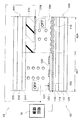
図1および図2に本発明の実施の形態に係る液晶表示装置50を説明する模式図を示す
。液晶表示装置50は、液晶パネル60と、液晶パネル60を駆動する駆動回路70と、
液晶パネル60に対向して配置された不図示のバックライト装置とを含んで構成されてい
る。なお、図1等では、液晶パネル60の1つの画素(ドット、サブピクセル等とも呼ば
れる)を断面図で示し、図面の煩雑化を避けるために一部の要素にのみハッチングを施し
ている。
1 and 2 are schematic diagrams illustrating a liquid
And a backlight device (not shown) disposed to face the
液晶パネル60は、1つの画素内に透過表示を行う透過部60Tと反射表示を行う反射
部60Rとを含んだ半透過型の液晶パネルである。なお、透過部60Tおよび反射部60
Rはそれぞれ、画素の平面視における2次元領域だけでなく、当該2次元領域を液晶パネ
ル60の厚さ方向すなわち後述の基板100,200の重ね合わせ方向に投影して規定さ
れる液晶パネル60の3次元領域をも指すものとする。
The
R is not only a two-dimensional region in a plan view of the pixel, but also the two-dimensional region of the
ここでは、液晶パネル60が、透過表示をFFS(Fringe Field Switching)方式によ
って行い、反射表示をECB(Electrically Controled Birefringence)方式によって行
う場合を例示する。
Here, a case where the
液晶パネル60は、素子基板100と、素子基板100に対向する対向基板200と、
両基板100,200間に設けられた液晶(または液晶層)300とを含んで構成されて
いる。なお、液晶300について液晶分子を模式的に図示している。
The
The liquid crystal (or liquid crystal layer) 300 provided between the
素子基板100は、透光性基板112を含んで構成され、さらに、透光性基板112よ
りも内側すなわち当該基板112に対して液晶層300の側に、回路層114と、平坦化
膜116と、反射膜118と、第1電極120と、絶縁膜122と、第2電極124と、
不図示の配向膜とを含んで構成されている。
The
And an alignment film (not shown).
透光性基板112は、例えば透明なガラス板で構成されている。
The
回路層114は、各種素子等が形成されて画素を駆動するための回路が形成された層で
あり、例えば画素TFT(Thin Film Transistor)や各種配線を含んで構成されている。
ここでは当該回路の詳細は省略するが、各種の回路が適用可能である。回路層114は透
光性基板112上に透過部60Tと反射部60Rとにわたって配置されている。
The
Although details of the circuit are omitted here, various circuits are applicable. The
平坦化膜116は、例えば絶縁性かつ透光性の樹脂で構成され、回路層114よりも液
晶層300の側に位置し回路層114上に配置されている。平坦化膜116は、透過部6
0Tと反射部60Rとにわたっている。平坦化膜116における対向基板200側の表面
は、透過部60T内では平坦であり、反射部60R内では凹凸形状になっている。当該凹
凸形状は、各種方法によって形成可能であり、例えば平坦化膜116をフォトレジスト材
料で構成し当該フォトレジスト材料のパターン露光および現像によって形成可能である。
The
It extends over 0T and the
反射膜118は、反射表示のために外光(可視光)を反射可能な材料、例えばアルミニ
ウム等で構成されている。反射膜118は、反射部60Rに配置され、平坦化膜116の
上記凹凸面上に配置されている。反射膜118の対向基板200側の表面は平坦化膜11
6の凹凸面と同様の凹凸形状になっている。
The
6 has an uneven shape similar to the uneven surface.
第1電極120は、例えばITO(Indium Tin Oxide)等の透光性導電材料で構成され
ている。第1電極120は、反射膜118を覆って平坦化膜116上に配置されている。
第1電極120は、透過部60Tと反射部60Rとにわたっており、すなわち透過部60
Tと反射部60Rとに共通の電極である。第1電極120の対向基板200側の表面は、
透過部60T内では平坦であり、反射部60R内では反射膜118および平坦化膜116
の凹凸面と同様の凹凸形状になっている。
The
The
It is an electrode common to T and the
It is flat in the
The uneven surface is the same as the uneven surface.
なお、上記の反射膜118が導電性を有する場合、第1電極120は反射膜118に接
続されている限り反射膜118の全体を覆わない形態でもよい。すなわち、第1電極12
0の反射部60R内の部分を反射膜118によって構成することも可能である。
Note that when the
It is also possible to configure the part in the
なお、図1等では説明のために第1電極120と駆動回路70との接続を模式的に図示
しているが、第1電極120への電位の印加は例えば回路層114内の上記画素TFT等
を介して行われる。
In FIG. 1 and the like, the connection between the
絶縁膜122は、例えば酸化シリコン、窒素シリコン等で構成されている。絶縁膜12
2は、透過部60T内において第1電極120の上記平坦面上に配置されている。絶縁膜
122の対向基板200側の表面は平坦である。
The insulating
2 is disposed on the flat surface of the
第2電極124は、例えばITO等の透光性導電材料で構成されている。第2電極12
4は、透過部60T内において絶縁膜122上に配置されており、絶縁膜122を介して
第1電極120に対向している。すなわち、第1電極120と絶縁膜122と第2電極1
24とがこの順序で積層されている。両電極124,120は、素子基板100に設けら
れているので、液晶層300に対して同じ側に位置している。第2電極124には第1電
極120に対向する部分にスリット126が設けられており、ここではスリット126は
図面の略垂直方向に延在している場合を例示する。第1電極120と第2電極124との
電位差に起因した電界ETがスリット126および絶縁膜122を介して発生する(図2
参照)。当該電界ETによって液晶300の透過部60T内での配向状態が制御される。
The
4 is disposed on the insulating
24 are stacked in this order. Since both
reference). The alignment state in the
なお、図1等では説明のために第2電極124と駆動回路70との接続を模式的に図示
しているが、第2電極124への電位の印加は例えば回路層114内の配線等を介して行
われる。
Note that in FIG. 1 and the like, the connection between the
不図示の配向膜は、第2電極124と絶縁膜122と第1電極120とを覆って配置さ
れ、液晶300に接している。
An alignment film (not shown) is disposed so as to cover the
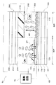
対向基板200は、透光性基板212を含んで構成され、さらに、透光性基板212よ
りも内側すなわち当該基板212に対して液晶300の側に、カラーフィルタ214と、
位相差層216と、第3電極218と、不図示の配向膜とを含んで構成されている。
The
The
透光性基板212は、例えば透明なガラス板で構成されている。
The
カラーフィルタ214は、例えば染色された樹脂で構成され、透過部60Tと反射部6
0Rとにわたって透光性基板212上に配置されている。カラーフィルタ214によって
、素子基板100側から入射したバックライト光および対向基板200側から入射した外
光が着色されて画素が所定の色に点灯する。カラーフィルタ214の色は各画素の表示色
(単色)に応じて設定されている。なお、近接する複数色の画素で構成される1単位はピ
クセル等と呼ばれ、当該1単位を画素と呼ぶ場合もある。
The
It is arranged on the
位相差層216は、ここでは半波長板(または1/2波長(2分の1波長)板)に相当
する場合を例示する。この場合、位相差層216によって直線偏光の偏光方向を右回りに
(または左回りに)45°回転させることが可能である。位相差層216は、カラーフィ
ルタ214よりも液晶層300の側に位置し、反射部60R内においてカラーフィルタ2
14上に配置されている。この場合、位相差層216は液晶パネル60に内蔵されている
。ここで、内蔵とは、透光性基板112,212間に配置された配置形態を言うものとす
る。このとき、例えば上記の画素TFT等も液晶パネル60に内蔵されていると捉えられ
る。
Here, the
14 is arranged. In this case, the
位相差層216は、例えばUV(紫外線)キュアラブル液晶(紫外線で硬化可能な液晶
)を利用して形成可能である。より具体的には、カラーフィルタ214上に配向膜(図示
せず)を形成し、当該配向膜上に液体状のUVキュアラブル液晶を塗布等し紫外線(UV
)を照射して硬化することによって、位相差層216を形成可能である。この場合、位相
差層216は、UVキュアラブル液晶を含んで構成され、あるいはさらに上記配向膜を含
んで構成される。なお、上記配向膜はUVキュアラブル液晶の配向を制御するものであり
、液晶300の配向を規定するものではない。UVキュアラブル液晶用の上記配向膜とし
て、各種の配向膜が利用可能である。例えば光照射によって液晶配向能を生じる光配向膜
を利用可能であり、当該光配向膜によればラビングが不要である。UVキュアラブル液晶
は、UVキュアを施す(UVを照射して硬化する)ことによって、位相差板として機能す
る。その位相差は、UVキュアラブル液晶の厚さを変えることで調整可能である。
The
) To cure, the
第3電極218は、例えばITO等の透光性導電材料で構成されている。第3電極21
8は、位相差層216よりも液晶層300の側に位置し反射部60R内において位相差層
216上に配置され、液晶層300を介して第1電極120に対向している。すなわち、
第3電極218は、液晶300に対して第1電極120とは反対側に位置している。第3
電極218と第1電極120との電位差に起因した電界ERによって液晶300の反射部
60R内の配向状態が制御される(図2参照)。
The
8 is located on the
The
The alignment state in the
第3電極218には、第2電極124と同じ電位が印加される。この電位印加の形態を
、図1等では駆動回路70からの配線が分岐して両電極218,124に至る場合を模式
的に例示している。この例示に代えて、分岐を液晶パネル60内に設けて両電極124,
218に同電位が印加可能な状態に構成してもよい。例えば、導電性粒子等を利用して液
晶パネル60内において両電極218,124を接続し電極124,218の一方へ駆動
回路70からの電位を印加するように構成してもよい。また、駆動回路70からの配線を
両電極218,124に対してそれぞれ設け各配線へ駆動回路70から同電位を出力する
ように構成してもよい。
The same potential as that of the
You may comprise in the state which can apply the same electric potential to 218. For example, the
不図示の配向膜は、第3電極218と位相差層216とカラーフィルタ214とを覆っ
て配置され、液晶300に接している。
An alignment film (not shown) is disposed so as to cover the
液晶パネル60は、さらに偏光板128,220を含んで構成されている。偏光板12
8は素子基板100の外側すなわち透光性基板112に対して液晶層300とは反対の側
に配置されている。偏光板220は対向基板200の外側すなわち透光性基板212に対
して液晶層300とは反対の側に配置されている。
The
8 is arranged outside the
駆動回路70は、電極120,124,218に接続されて電極120,124,21
8への印加電位を生成、伝達等するための各種要素を含んで構成されている。当該各種要
素は、液晶パネル60に外付けされ、または内蔵され、または実装されており、例えば回
路層114内の画素TFT等も含まれるものとする。駆動回路70は、上記印加電位を生
成し所定のタイミングで電極120,124,218へ印加する。
The
8 includes various elements for generating, transmitting, and the like, the potential applied to 8. The various elements are externally attached to, built in, or mounted on the
次に、図1および図2を参照しつつ、液晶表示装置50の動作の一例を説明する。ここ
では上記のように透過表示をFFS方式によって行い反射表示をECB方式によって行う
場合を例示する。なお、液晶300は、例えば、誘電異方性が正であり、屈折率異方性(
複屈折性とも呼ばれる)Δnは0.1である。
Next, an example of the operation of the liquid
Δn (also called birefringence) is 0.1.
液晶パネル60は、第1電極120と第2電極124との電位差がオフ(OFF)電圧
の場合に透過表示が輝度の最も低い状態である暗表示になるように構成されているととも
に、第1電極120と第3電極218との電位差がオフ電圧の場合に反射表示が暗表示に
なるように構成されている(図1参照)。なお、透過表示についての輝度は透過率に対応
し、反射表示についての輝度は反射率に対応する。また、暗表示は暗状態、黒表示等とも
呼ばれる。また、最も輝度の高い状態を明表示とよぶことにする。明表示は明状態、白表
示等とも呼ばれる。また、暗表示または明表示を実現する電圧であって電界ET,ERを
ほとんど発生させない電圧をオフ電圧と呼び、これに対して暗表示または明表示を実現す
る電圧であってオフ電圧印加時に比べて大きな電界ET,ERが発生する電圧をオン(O
N)電圧と呼ぶことにする。
The
N) Let's call it voltage.
このため、ここでは、透過部60Tおよび反射部60Rの両方がノーマリブラック方式
(Normaly Black Type)に構成され、画素全体としてもノーマリブラック方式に構成され
ている。このような構成は、液晶300の材料、オフ電圧印加時における液晶300の配
向状態(いわゆる初期配向状態)、配向膜のラビング方向、偏光板128,220および
位相差層216の特性や配置、等の調整によって可能である。
For this reason, here, both the
液晶表示装置50では、第2電極124と第3電極218とに同電位が印加されるので
、オフ電圧の印加によって透過部60Tおよび反射部60Rは同時に暗表示になる。すな
わち画素全体が暗表示になる。他方、オン電圧の印加によって透過部60Tおよび反射部
60Rを同時に明表示にすることが可能であり、このとき画素全体が明表示になる(図2
参照)。
In the liquid
reference).
より具体的な一例を以下に説明する。 A more specific example will be described below.
例えば、オフ電圧印加時において、透過部60T内および反射部60R内で液晶300
を液晶分子の長軸が電極120,124,218の表面に略平行になるようにかつスリッ
ト126の延在方向に略平行に初期配向させる(したがって図面の略垂直方向に配向させ
る)。なお、透過部60Tと反射部60Rとでラビング方向は同じに設定されている。ま
た、偏光板128を透過軸が初期配向状態の液晶分子の長軸に略直交するように配置する
。また、偏光板128の透過軸と透過軸を略直交させて偏光板220を配置する(いわゆ
る直交配置)。
For example, when the off voltage is applied, the
Are initially aligned so that the major axis of the liquid crystal molecules is substantially parallel to the surfaces of the
この場合、透過表示について、素子基板100側から入射したバックライト光は、偏光
板128によって液晶分子の長軸に略直交する直線偏光になる。当該直線偏光の偏光方向
と液晶分子の配向方向との関係によれば液晶300の複屈折効果をほとんど受けないので
、当該直線偏光は偏光状態を保ったまま偏光板220へ到達する。しかし、当該直線偏光
は偏光板220の透過軸と略直交する方向に偏光しているので、偏光板220を透過する
ことができず、その結果、透過表示は暗表示になる。
In this case, in the transmissive display, the backlight light incident from the
反射表示については、対向基板200側から入射した外光は、偏光板220によって液
晶分子の長軸に略平行な直線偏光になり、位相差層216の上記作用によって偏光方向が
45°回転し、その偏光状態で液晶層300へ進入する。反射部60Rの液晶層300は
その複屈折性を利用して1/4波長(4分の1波長)板と同様に作用するように調整され
ている。この場合、液晶層300によって直線偏光が右回り(または左回り)の略円偏光
に変換される。液晶層300によって略円偏光とされた外光は、反射膜118で反射し、
液晶層300を通過して位相差層216から液晶層300に入射した直線偏光に対して9
0°回転した直線偏光になり、位相差層216によって偏光方向が−45°回転して、偏
光板220へ到達する。しかし、偏光板220へ戻ってきた直線偏光は偏光板220の透
過軸と略直交する方向に偏光している。したがって、偏光板220を透過することができ
ず、その結果、反射表示は暗表示になる。
For reflective display, external light incident from the
For linearly polarized light that has passed through the
The light is linearly polarized light rotated by 0 °, and the polarization direction is rotated by −45 ° by the
他方、オフ電圧からオン電圧へ変化させると、透過表示は暗表示を脱し、反射表示も暗
表示を脱する(図2参照)。なお、印加電圧の増大に伴って透過表示および反射表示の輝
度が上昇する。
On the other hand, when the off voltage is changed to the on voltage, the transmissive display is removed from the dark display, and the reflective display is also removed from the dark display (see FIG. 2). Note that the luminance of the transmissive display and the reflective display increases as the applied voltage increases.
透過部60Tでは、オン電圧の印加によって、素子基板100付近の液晶分子は、電極
120,124の表面に略平行にかつスリット126の延在方向に略直交する方向に液晶
分子が配向する。その一方で、対向基板200付近の液晶分子は初期配向状態のままであ
る。このため、透過部60T内の液晶分子は全体として電極124,120の法線回りに
90°ねじれた状態に配向する。この場合、偏光板128によって直線偏光になったバッ
クライト光は、素子基板100付近の液晶分子の長軸に略平行な方向に偏光しており、液
晶分子の上記ねじれた配向状態に従って旋光(回転)し、偏光板220へ到達した時点で
は対向基板200付近の液晶分子の長軸に略平行な直線偏光になる。当該直線偏光は、偏
光板220の透過軸と略平行に偏光しているので、その結果、透過表示は明表示になる。
In the
反射部60Rでは、オン電圧の印加によって、液晶分子は電極120,218の表面に
略直交する方向に配向する。対向基板200側から入射した外光は、暗表示時と同様の経
路(光路)を辿って偏光板220へ戻ってくるが、上記配向状態によれば液晶300の複
屈折効果の影響をほとんど受ない。このため、偏光板220へ戻ってきた外光は、位相差
層216における偏光方向の回転作用を往復で合計2回受けた結果、偏光板220の透過
軸に略平行な直線偏光になっている。したがって、偏光板220を透過し、その結果、反
射表示は明表示になる。
In the
上記では暗表示および明表示の場合を説明したが、印加電圧の大きさの制御によって暗
表示と明表示との間のレベルの輝度、いわゆる中間調表示を行うことも可能である。
The case of dark display and bright display has been described above, but it is also possible to perform so-called halftone display at a level between dark display and bright display by controlling the magnitude of the applied voltage.
上記構成によれば、透過部60TがFFS方式であり、反射部60RがECB方式であ
るため、反射表示および透過表示の両方において、良好な表示を得ることができる。また
、内面の反射部に位相差層を形成する構成とすると、位相差板を外面に貼る必要がなく、
他の方式の半透過型に比べて液晶パネルを薄くすることが可能となる。さらに、位相差層
216が透過部60Tのセルギャップより反射部60Rのセルギャップを狭くするための
層を兼ねることにより、製造工程を減らすことができる。
According to the above configuration, since the
The liquid crystal panel can be made thinner than other transflective types. Furthermore, since the
また、反射部60RをFFS方式よりも反射率の高いECB方式で構成しているので、
透過部60Tと反射部60Rとの両方をFFS方式で構成する場合に比べて、高輝度の反
射表示を得ることができる。
In addition, since the
Compared with the case where both the
さらに、反射部60RにFFS方式を採用していないので、平坦化膜116に上記凹凸
面を形成する場合であっても、スリット126を有した電極124を当該凹凸面上に形成
する必要がない。このため、凹凸面上におけるスリットのパターニング不具合が発生せず
、良好な反射表示が得られる。また、透過表示についてはFFS方式によって広視野角、
高コントラスト等が実現される。
Further, since the FFS method is not adopted for the reflecting
High contrast and the like are realized.
また、FFS方式では一般的に対向基板の外面にITO膜等を形成して外部からの電界
をシールドすることが多いが、上記構成によればシールド構造を外部に設ける必要がない
。なぜならば、対向基板200の第3電極218がシールド作用を奏するからである。な
お、対向基板200の全面にすきま無く設けられていなくても第3電極218によってシ
ールド作用を得ることは可能である。
In the FFS method, an ITO film or the like is generally formed on the outer surface of the counter substrate to shield an electric field from the outside. However, according to the above configuration, it is not necessary to provide a shield structure outside. This is because the
また、位相差層216は透過部60Tには設けられていないので、透過部60Tと反射
部60Rとを区別することなく全面的に外付けした場合とは異なり、透過表示についてF
FS方式による広視野角、高コントラスト等が確保される。
In addition, since the
A wide viewing angle, high contrast, etc. are ensured by the FS method.
また、位相差層216によって反射部60Rでのセルギャップが透過部60Tでのセル
ギャップよりも狭められている(いわゆるマルチギャップ構造)。例えば、透過部60T
のセルギャップは3.0μmであり、反射部60Rのセルギャップは1.4μmである。
このため、別途のトップコート層を用いなくても、透過部60Tと反射部60Rとでセル
ギャップを調整することができる。例えば、反射部60RのセルギャップをECB方式に
適した値に調整することができる。
Moreover, the cell gap in the
The cell gap of the
Therefore, the cell gap can be adjusted between the
なお、上記では透過表示をFFS方式によって行う場合を例示したが、透過表示をIP
S(In-Plane Switching)方式によって行う構成にすることも可能である。IPS方式の
場合、図3に示すように、透過部60Tにおいて第1電極120と第2電極124とは平
坦化膜116上に、すなわち同層に配置される。なお、図3には画素全体が明表示時の状
態を例示している。
In addition, although the case where the transmissive display is performed by the FFS method is illustrated above, the transmissive display is IP
It is also possible to adopt a configuration that is performed by an S (In-Plane Switching) method. In the case of the IPS method, as shown in FIG. 3, the
また、偏光板128,220を互いの透過軸を略平行にして配置することによって、ノ
ーマリホワイト方式(Normaly White Type)を構成することも可能である。
Also, it is possible to configure a normally white type by arranging the
50…液晶表示装置、60T…透過部、60R…反射部、100…素子基板、120…
第1電極、124…第2電極、200…対向基板、216…位相差層、218…第3電極
、300…液晶、ET,ER…電界。
50 ... Liquid crystal display device, 60T ... Transmission part, 60R ... Reflection part, 100 ... Element substrate, 120 ...
1st electrode, 124 ... 2nd electrode, 200 ... Counter substrate, 216 ... Retardation layer, 218 ... 3rd electrode, 300 ... Liquid crystal, ET, ER ... Electric field.
Claims (4)
前記第1基板の前記液晶とは反対側に第1偏光板を備え、
前記第2基板の前記液晶とは反対側に第2偏光板を備え、
前記第1基板と前記液晶を介して対向する前記第2基板に第3電極を備え、
前記第1電極は、前記透過部と前記反射部とにわたって設けられ、前記第2電極は、前記第1基板の一方向に延在するスリットを有し、前記透過部内において絶縁膜を介して前記第1電極と対向して配置され、前記第3電極は、前記反射部内において前記液晶を介して前記第1電極と対向して配置され、
前記液晶は、前記透過部および前記反射部内の液晶分子の長軸が前記第1電極の表面に略平行であって、かつ前記第2電極の前記スリットの延在方向に略平行に初期配向されるとともに、前記透過部では前記第1電極と前記第2電極との電界で配向制御され、前記反射部では前記第1電極と前記第3電極との電界で配向制御され、
前記反射部に配置された位相差層は、1/2波長板であり、
前記第1偏光板の透過軸は、前記第1電極と前記第2電極との電位差がオフ電圧となる前記透過部の暗表示において、前記第1偏光板に入射した光が前記液晶の液晶分子の長軸に対して略直交な偏光として前記液晶に入射するように配置される、液晶表示装置。 The liquid crystal sandwiched between the first substrate and the second substrate has a transmissive portion for performing transmissive display in one pixel and a reflective portion for performing reflective display, the a first electrode and a second electrode A liquid crystal display device provided on the first substrate,
A first polarizing plate on the opposite side of the first substrate from the liquid crystal;
A second polarizing plate on the opposite side of the second substrate from the liquid crystal;
A third electrode on the second substrate facing the first substrate via the liquid crystal;
The first electrode is provided across the transmissive part and the reflective part, and the second electrode has a slit extending in one direction of the first substrate, and the insulating film is interposed in the transmissive part via an insulating film. Arranged to face the first electrode, the third electrode is arranged to face the first electrode via the liquid crystal in the reflection portion,
The liquid crystal is initially aligned so that the major axis of the liquid crystal molecules in the transmissive part and the reflective part is substantially parallel to the surface of the first electrode and substantially parallel to the extending direction of the slit of the second electrode. And the orientation is controlled by the electric field between the first electrode and the second electrode in the transmission part, and the orientation is controlled by the electric field between the first electrode and the third electrode in the reflection part.
The retardation layer disposed in the reflecting portion is a half-wave plate,
The transmission axis of the first polarizing plate is such that light incident on the first polarizing plate is a liquid crystal molecule of the liquid crystal in the dark display of the transmissive portion where the potential difference between the first electrode and the second electrode is an off voltage. A liquid crystal display device disposed so as to be incident on the liquid crystal as polarized light substantially perpendicular to the major axis.
前記第1偏光板の透過軸と前記第2偏光板の透過軸とは略直交に配置される、液晶表示装置。 The liquid crystal display device according to claim 1,
A liquid crystal display device , wherein a transmission axis of the first polarizing plate and a transmission axis of the second polarizing plate are arranged substantially orthogonal to each other .
前記位相差層は前記第2基板の前記液晶側に設けられ、前記第2偏光板より入射した直線偏光の偏光方向を45°回転させる、液晶表示装置。 The liquid crystal display device, wherein the retardation layer is provided on the liquid crystal side of the second substrate and rotates the polarization direction of linearly polarized light incident from the second polarizing plate by 45 °.
前記第2電極と前記第3電極とに同一の電位が印加される、液晶表示装置。A liquid crystal display device, wherein the same potential is applied to the second electrode and the third electrode.
Priority Applications (1)
| Application Number | Priority Date | Filing Date | Title |
|---|---|---|---|
| JP2009059043A JP5397989B2 (en) | 2009-03-12 | 2009-03-12 | Liquid crystal display |
Applications Claiming Priority (1)
| Application Number | Priority Date | Filing Date | Title |
|---|---|---|---|
| JP2009059043A JP5397989B2 (en) | 2009-03-12 | 2009-03-12 | Liquid crystal display |
Related Parent Applications (1)
| Application Number | Title | Priority Date | Filing Date |
|---|---|---|---|
| JP2006252658A Division JP2008076501A (en) | 2006-09-19 | 2006-09-19 | Liquid crystal display |
Publications (3)
| Publication Number | Publication Date |
|---|---|
| JP2009122716A JP2009122716A (en) | 2009-06-04 |
| JP2009122716A5 JP2009122716A5 (en) | 2009-10-08 |
| JP5397989B2 true JP5397989B2 (en) | 2014-01-22 |
Family
ID=40814842
Family Applications (1)
| Application Number | Title | Priority Date | Filing Date |
|---|---|---|---|
| JP2009059043A Active JP5397989B2 (en) | 2009-03-12 | 2009-03-12 | Liquid crystal display |
Country Status (1)
| Country | Link |
|---|---|
| JP (1) | JP5397989B2 (en) |
Families Citing this family (2)
| Publication number | Priority date | Publication date | Assignee | Title |
|---|---|---|---|---|
| CN102662272A (en) * | 2012-04-12 | 2012-09-12 | 华映视讯(吴江)有限公司 | Semi-penetration and semi-reflection liquid crystal display and liquid crystal panel of semi-penetration and semi-reflection liquid crystal display |
| JP6496172B2 (en) | 2015-03-31 | 2019-04-03 | 大和ハウス工業株式会社 | Video display system and video display method |
Family Cites Families (7)
| Publication number | Priority date | Publication date | Assignee | Title |
|---|---|---|---|---|
| JP3681775B2 (en) * | 1995-01-09 | 2005-08-10 | アルプス電気株式会社 | Liquid crystal display element |
| JPH1090704A (en) * | 1996-09-10 | 1998-04-10 | Advanced Display:Kk | Display panel of liquid crystal display device |
| JP2001318381A (en) * | 2000-05-09 | 2001-11-16 | Matsushita Electric Ind Co Ltd | Liquid crystal display panel |
| JP2005257904A (en) * | 2004-03-10 | 2005-09-22 | Mitsubishi Electric Corp | Liquid crystal display device |
| JP4223992B2 (en) * | 2004-05-25 | 2009-02-12 | 株式会社 日立ディスプレイズ | Liquid crystal display |
| JP4816862B2 (en) * | 2004-12-16 | 2011-11-16 | ソニー株式会社 | Liquid crystal display |
| JP2008076501A (en) * | 2006-09-19 | 2008-04-03 | Epson Imaging Devices Corp | Liquid crystal display |
-
2009
- 2009-03-12 JP JP2009059043A patent/JP5397989B2/en active Active
Also Published As
| Publication number | Publication date |
|---|---|
| JP2009122716A (en) | 2009-06-04 |
Similar Documents
| Publication | Publication Date | Title |
|---|---|---|
| TWI407213B (en) | Liquid crystal display device | |
| US7995168B2 (en) | Transflective liquid crystal display having a relationship between the electrode spacing and cell gap in the reflection and transmission regions | |
| US8169555B2 (en) | Liquid crystal display device | |
| US8094267B2 (en) | Liquid crystal display device, methods for manufacturing the same, and electronic apparatus | |
| JP2006317905A (en) | Semi-transparent type fringe field switching mode liquid crystal display device | |
| US20080309861A1 (en) | Liquid crystal device and electronic apparatus | |
| JP4337854B2 (en) | Liquid crystal display | |
| KR100866942B1 (en) | Liquid crystal display device | |
| KR20070068772A (en) | Liquid crystal display device and fabricating method thereof | |
| JP2009258332A (en) | Liquid crystal display device and electronic device | |
| KR20050068880A (en) | Device and fabrication method for liquid crystal display of multi domain | |
| JP5397989B2 (en) | Liquid crystal display | |
| KR20080083791A (en) | Transflective type liquid crystal display device and method for fabricating the same | |
| KR101117988B1 (en) | Trans-flective Type Liquid Crystal Display Device | |
| JP2008076503A (en) | Liquid crystal display | |
| KR20090032467A (en) | Transflective type liquid crystal display device | |
| JP5041436B2 (en) | Liquid crystal display | |
| JP4824443B2 (en) | Liquid crystal display | |
| KR101335525B1 (en) | Liquid crystal display device and method of fabricating the same | |
| KR20080086118A (en) | Transflective type liquid crystal display device and method for fabricating the same | |
| KR102224092B1 (en) | Trans-flective mode liquidcrystal display device | |
| JP2008170675A (en) | Liquid crystal device and electronic device | |
| KR101332155B1 (en) | Liquid Crystal Device of Transflective In Plane Switch Type And Method for Fabricating thereof | |
| JP2008310179A (en) | Liquid crystal display device | |
| KR20060028098A (en) | Array substrate and display apparatus having the same |
Legal Events
| Date | Code | Title | Description |
|---|---|---|---|
| A521 | Request for written amendment filed |
Free format text: JAPANESE INTERMEDIATE CODE: A523 Effective date: 20090821 |
|
| A621 | Written request for application examination |
Free format text: JAPANESE INTERMEDIATE CODE: A621 Effective date: 20090821 |
|
| A711 | Notification of change in applicant |
Free format text: JAPANESE INTERMEDIATE CODE: A711 Effective date: 20100526 |
|
| RD02 | Notification of acceptance of power of attorney |
Free format text: JAPANESE INTERMEDIATE CODE: A7422 Effective date: 20100526 |
|
| A521 | Request for written amendment filed |
Free format text: JAPANESE INTERMEDIATE CODE: A523 Effective date: 20100630 |
|
| A711 | Notification of change in applicant |
Free format text: JAPANESE INTERMEDIATE CODE: A711 Effective date: 20120330 |
|
| A131 | Notification of reasons for refusal |
Free format text: JAPANESE INTERMEDIATE CODE: A131 Effective date: 20120508 |
|
| A521 | Request for written amendment filed |
Free format text: JAPANESE INTERMEDIATE CODE: A523 Effective date: 20120621 |
|
| A131 | Notification of reasons for refusal |
Free format text: JAPANESE INTERMEDIATE CODE: A131 Effective date: 20130108 |
|
| A521 | Request for written amendment filed |
Free format text: JAPANESE INTERMEDIATE CODE: A523 Effective date: 20130306 |
|
| RD03 | Notification of appointment of power of attorney |
Free format text: JAPANESE INTERMEDIATE CODE: A7423 Effective date: 20130328 |
|
| TRDD | Decision of grant or rejection written | ||
| A01 | Written decision to grant a patent or to grant a registration (utility model) |
Free format text: JAPANESE INTERMEDIATE CODE: A01 Effective date: 20131001 |
|
| A711 | Notification of change in applicant |
Free format text: JAPANESE INTERMEDIATE CODE: A712 Effective date: 20131018 |
|
| A61 | First payment of annual fees (during grant procedure) |
Free format text: JAPANESE INTERMEDIATE CODE: A61 Effective date: 20131018 |
|
| R150 | Certificate of patent or registration of utility model |
Ref document number: 5397989 Country of ref document: JP Free format text: JAPANESE INTERMEDIATE CODE: R150 Free format text: JAPANESE INTERMEDIATE CODE: R150 |
|
| R250 | Receipt of annual fees |
Free format text: JAPANESE INTERMEDIATE CODE: R250 |
|
| R250 | Receipt of annual fees |
Free format text: JAPANESE INTERMEDIATE CODE: R250 |
|
| R250 | Receipt of annual fees |
Free format text: JAPANESE INTERMEDIATE CODE: R250 |
|
| R250 | Receipt of annual fees |
Free format text: JAPANESE INTERMEDIATE CODE: R250 |
|
| R250 | Receipt of annual fees |
Free format text: JAPANESE INTERMEDIATE CODE: R250 |
|
| R250 | Receipt of annual fees |
Free format text: JAPANESE INTERMEDIATE CODE: R250 |
|
| R250 | Receipt of annual fees |
Free format text: JAPANESE INTERMEDIATE CODE: R250 |
|
| R250 | Receipt of annual fees |
Free format text: JAPANESE INTERMEDIATE CODE: R250 |