EP2322692A1 - Etchant for titanium-based metal, tungsten-based metal, titanium-tungsten-based metal or nitrides thereof - Google Patents
Etchant for titanium-based metal, tungsten-based metal, titanium-tungsten-based metal or nitrides thereof Download PDFInfo
- Publication number
- EP2322692A1 EP2322692A1 EP09813013A EP09813013A EP2322692A1 EP 2322692 A1 EP2322692 A1 EP 2322692A1 EP 09813013 A EP09813013 A EP 09813013A EP 09813013 A EP09813013 A EP 09813013A EP 2322692 A1 EP2322692 A1 EP 2322692A1
- Authority
- EP
- European Patent Office
- Prior art keywords
- titanium
- tungsten
- based metals
- etching
- metals
- Prior art date
- Legal status (The legal status is an assumption and is not a legal conclusion. Google has not performed a legal analysis and makes no representation as to the accuracy of the status listed.)
- Granted
Links
Images


Classifications
-
- C—CHEMISTRY; METALLURGY
- C23—COATING METALLIC MATERIAL; COATING MATERIAL WITH METALLIC MATERIAL; CHEMICAL SURFACE TREATMENT; DIFFUSION TREATMENT OF METALLIC MATERIAL; COATING BY VACUUM EVAPORATION, BY SPUTTERING, BY ION IMPLANTATION OR BY CHEMICAL VAPOUR DEPOSITION, IN GENERAL; INHIBITING CORROSION OF METALLIC MATERIAL OR INCRUSTATION IN GENERAL
- C23F—NON-MECHANICAL REMOVAL OF METALLIC MATERIAL FROM SURFACE; INHIBITING CORROSION OF METALLIC MATERIAL OR INCRUSTATION IN GENERAL; MULTI-STEP PROCESSES FOR SURFACE TREATMENT OF METALLIC MATERIAL INVOLVING AT LEAST ONE PROCESS PROVIDED FOR IN CLASS C23 AND AT LEAST ONE PROCESS COVERED BY SUBCLASS C21D OR C22F OR CLASS C25
- C23F1/00—Etching metallic material by chemical means
- C23F1/10—Etching compositions
- C23F1/14—Aqueous compositions
- C23F1/32—Alkaline compositions
- C23F1/38—Alkaline compositions for etching refractory metals
-
- C—CHEMISTRY; METALLURGY
- C23—COATING METALLIC MATERIAL; COATING MATERIAL WITH METALLIC MATERIAL; CHEMICAL SURFACE TREATMENT; DIFFUSION TREATMENT OF METALLIC MATERIAL; COATING BY VACUUM EVAPORATION, BY SPUTTERING, BY ION IMPLANTATION OR BY CHEMICAL VAPOUR DEPOSITION, IN GENERAL; INHIBITING CORROSION OF METALLIC MATERIAL OR INCRUSTATION IN GENERAL
- C23F—NON-MECHANICAL REMOVAL OF METALLIC MATERIAL FROM SURFACE; INHIBITING CORROSION OF METALLIC MATERIAL OR INCRUSTATION IN GENERAL; MULTI-STEP PROCESSES FOR SURFACE TREATMENT OF METALLIC MATERIAL INVOLVING AT LEAST ONE PROCESS PROVIDED FOR IN CLASS C23 AND AT LEAST ONE PROCESS COVERED BY SUBCLASS C21D OR C22F OR CLASS C25
- C23F1/00—Etching metallic material by chemical means
- C23F1/10—Etching compositions
- C23F1/14—Aqueous compositions
- C23F1/16—Acidic compositions
- C23F1/26—Acidic compositions for etching refractory metals
-
- C—CHEMISTRY; METALLURGY
- C23—COATING METALLIC MATERIAL; COATING MATERIAL WITH METALLIC MATERIAL; CHEMICAL SURFACE TREATMENT; DIFFUSION TREATMENT OF METALLIC MATERIAL; COATING BY VACUUM EVAPORATION, BY SPUTTERING, BY ION IMPLANTATION OR BY CHEMICAL VAPOUR DEPOSITION, IN GENERAL; INHIBITING CORROSION OF METALLIC MATERIAL OR INCRUSTATION IN GENERAL
- C23F—NON-MECHANICAL REMOVAL OF METALLIC MATERIAL FROM SURFACE; INHIBITING CORROSION OF METALLIC MATERIAL OR INCRUSTATION IN GENERAL; MULTI-STEP PROCESSES FOR SURFACE TREATMENT OF METALLIC MATERIAL INVOLVING AT LEAST ONE PROCESS PROVIDED FOR IN CLASS C23 AND AT LEAST ONE PROCESS COVERED BY SUBCLASS C21D OR C22F OR CLASS C25
- C23F1/00—Etching metallic material by chemical means
- C23F1/10—Etching compositions
- C23F1/14—Aqueous compositions
- C23F1/32—Alkaline compositions
- C23F1/40—Alkaline compositions for etching other metallic material
-
- C—CHEMISTRY; METALLURGY
- C23—COATING METALLIC MATERIAL; COATING MATERIAL WITH METALLIC MATERIAL; CHEMICAL SURFACE TREATMENT; DIFFUSION TREATMENT OF METALLIC MATERIAL; COATING BY VACUUM EVAPORATION, BY SPUTTERING, BY ION IMPLANTATION OR BY CHEMICAL VAPOUR DEPOSITION, IN GENERAL; INHIBITING CORROSION OF METALLIC MATERIAL OR INCRUSTATION IN GENERAL
- C23F—NON-MECHANICAL REMOVAL OF METALLIC MATERIAL FROM SURFACE; INHIBITING CORROSION OF METALLIC MATERIAL OR INCRUSTATION IN GENERAL; MULTI-STEP PROCESSES FOR SURFACE TREATMENT OF METALLIC MATERIAL INVOLVING AT LEAST ONE PROCESS PROVIDED FOR IN CLASS C23 AND AT LEAST ONE PROCESS COVERED BY SUBCLASS C21D OR C22F OR CLASS C25
- C23F1/00—Etching metallic material by chemical means
- C23F1/44—Compositions for etching metallic material from a metallic material substrate of different composition
-
- C—CHEMISTRY; METALLURGY
- C23—COATING METALLIC MATERIAL; COATING MATERIAL WITH METALLIC MATERIAL; CHEMICAL SURFACE TREATMENT; DIFFUSION TREATMENT OF METALLIC MATERIAL; COATING BY VACUUM EVAPORATION, BY SPUTTERING, BY ION IMPLANTATION OR BY CHEMICAL VAPOUR DEPOSITION, IN GENERAL; INHIBITING CORROSION OF METALLIC MATERIAL OR INCRUSTATION IN GENERAL
- C23G—CLEANING OR DE-GREASING OF METALLIC MATERIAL BY CHEMICAL METHODS OTHER THAN ELECTROLYSIS
- C23G1/00—Cleaning or pickling metallic material with solutions or molten salts
- C23G1/14—Cleaning or pickling metallic material with solutions or molten salts with alkaline solutions
- C23G1/20—Other heavy metals
- C23G1/205—Other heavy metals refractory metals
-
- H—ELECTRICITY
- H10—SEMICONDUCTOR DEVICES; ELECTRIC SOLID-STATE DEVICES NOT OTHERWISE PROVIDED FOR
- H10P—GENERIC PROCESSES OR APPARATUS FOR THE MANUFACTURE OR TREATMENT OF DEVICES COVERED BY CLASS H10
- H10P50/00—Etching of wafers, substrates or parts of devices
- H10P50/60—Wet etching
- H10P50/66—Wet etching of conductive or resistive materials
- H10P50/663—Wet etching of conductive or resistive materials by chemical means only
- H10P50/667—Wet etching of conductive or resistive materials by chemical means only by liquid etching only
Definitions
- the present invention relates to an etching solution for titanium-based metals, tungsten-based metals, titanium/tungsten-based metals, or their nitrides.
- the invention relates to an etching solution with excellent selective etching properties for titanium-based metals, tungsten-based metals, titanium/tungsten-based metals or their nitrides, with respect to metals other than titanium-based metals, tungsten-based metals and titanium/tungsten-based metals.
- Titanium metal (Ti), titanium nitride (TiN) and titanium alloys, as titanium-based metals, are utilized for semiconductor devices, liquid crystal displays, MEMS (Micro Electro Mechanical Systems), printed wiring boards and the like, and as ground layers and cap layers for precious metal, aluminum (Al) and copper (Cu) wiring. In semiconductor devices, they are also used as barrier metals and gate metals.
- Hydrogen peroxide/ammonia/EDTA ethylenediaminetetraacetic acid
- hydrogen peroxide/phosphate mixtures have been disclosed as means of overcoming the drawbacks of such solutions (PTL 1 and 2).
- these have low titanium-based metal etching rates, while decomposition of hydrogen peroxide is rapid, making stable etching impossible, and therefore etching solutions comprising hydrogen peroxide/phosphoric acid/ammonia mixtures have been proposed as modifications of such solutions (PTL 3).
- etching solutions With such etching solutions, however, the etching rate is improved but intense foaming of the etching solution causes attachment of bubbles onto the substrate surface, and etching does not proceed at the bubble-attached parts.
- Another problem is the low etching rate due to foaming and decomposition of the hydrogen peroxide water.
- Such mixtures are used with adjustment to a designated pH with ammonia, but even slight differences in pH alter the etching rate and foaming condition, and can be problematic from the viewpoint of stability of the etching conditions.
- a semiconductor cleaning solution comprising an organic acid ammonium salt in hydrogen peroxide/ammonia/water, as a hydrogen peroxide-containing cleaning solution (PTL 4).
- the semiconductor cleaning solution is a cleaning solution that removes extraneous contaminant such as fine particles adhering to the substrate in the semiconductor production process, and although it is stated that the difference in etching rates between doped oxide films and non-doped oxide films is minimal, nothing at all is mentioned regarding etching of titanium-based metals.
- a composition for removal of resist residue comprising hydrogen peroxide/carboxylate/water. The purpose of the composition is removal of resist residue after ashing of the resist, and it is not intended for etching of titanium-based metals.
- Tungsten or tungsten alloys are used for gate electrodes of thin-film transistors, wirings, barrier layers, or for filling of contact holes or via holes in liquid crystal displays and semiconductor devices. They are also used as tungsten heaters in MEMS (Micro Electro Mechanical Systems).
- Tungsten or tungsten alloys are usually formed into films by CVD or sputtering. When films are formed by these methods, however, they also adhere on substrate (wafer) back sides, on substrate (wafer) edges, on the external walls of film-forming apparatuses and in exhaust pipes, in addition to the actual element-forming areas in the semiconductor devices, and they peel off and cause to produce extraneous material on the element-forming areas. This is sometimes countered by removing the unwanted film with an etching solution. In addition, to measures against extraneous material, it is preferable to employ highly productive wet etching instead of dry etching for tungsten or tungsten alloys in the production steps of semiconductor devices, liquid crystal display apparatuses and MEMS devices. Wet etching is particularly suitable for liquid crystal displays and MEMS devices which do not require the same level of working precision as semiconductor devices.
- etching solutions Mixtures of hydrofluoric acid and nitric acid are widely known as etching solutions and removing solutions for tungsten-based metals (Non-PTL 1, for example), but these are not preferred because silicon substrates or silicon dioxide films and glass substrates also dissolve. Another problem is that metals that are prone to corrosion, such as Al wirings, in the devices are also etched.
- Hydrogen peroxide water-based etching solutions are also known from PTL 6-9, for example, and PTL 9 summarizes in detail the problems of conventional hydrogen peroxide-based etching solutions. According to this publication, the etching speed is slow and the pH varies as tungsten dissolves, resulting in a variable etching rate and poor etching selectivity.
- the invention which overcomes the problems mentioned above, provides an etching solution for titanium-based metals, tungsten-based metals, titanium/tungsten-based metals or their nitrides, which reduces non-uniform etching of targets to be etched and has a stable etching rate, by minimizing foaming of the etching solution during etching.
- it provides an etching solution with no corrosion of substrates and with excellent selective etching properties for titanium-based metals, tungsten-based metals, titanium/tungsten-based metals or their nitrides, with respect to metals other than titanium-based metals, tungsten-based metals and titanium/tungsten-based metals.
- an aqueous solution comprising hydrogen peroxide and an organic acid salt can minimize foaming of the etching solution and reduce non-uniform etching of targets to be etched, and can stabilize the etching rate. It was further found that using an etching solution of the invention allows selective etching of titanium-based metals, tungsten-based metals, titanium/tungsten-based metals or their nitrides, without etching of other metals such as nickel, copper or aluminum or base materials (glass, silicon, silicon oxide, silicon nitride), and the present invention has been completed upon this finding.
- the invention comprises the following aspects, for example.
- the etching solution of the invention has an excellent selective etching property for titanium-based metals, tungsten-based metals, titanium/tungsten-based metals or their nitrides, with respect to metals other than titanium-based metals, tungsten-based metals and titanium/tungsten-based metals, or base materials (glass, silicon, silicon oxide), as well as little foaming, and therefore using the etching solution on the invention allows uniform etching to be accomplished for titanium-based metals, tungsten-based metals, titanium/tungsten-based metals or their nitrides.
- the etching solution for titanium-based metals, tungsten-based metals, titanium/tungsten-based metals or their nitrides comprises an aqueous solution containing hydrogen peroxide and an organic acid salt.
- the hydrogen peroxide is present in the etching solution at 10-40 mass%, more preferably 15-35 mass% and even more preferably 20-35 mass%. If the hydrogen peroxide concentration is lower than 10 mass%, the etching rate for titanium, tungsten or titanium/tungsten alloys will be reduced, making it impractical. If the hydrogen peroxide concentration is higher than 40 mass%, on the other hand, more hydrogen peroxide will decompose, likewise making it impractical.
- organic acid salts useful for the invention are not particularly limited, but when an organic acid salt is used for production of an electronic device such as a semiconductor which is preferably void of metal impurities, it is more preferred to use an ammonium salt.
- the organic acid salt is present in the etching solution at 0.1-15 mass%, more preferably 1-10 masses% and even more preferably 3-8 mass%. If the organic acid salt concentration is lower than 0.1 mass%, the etching rate will be reduced, making it impractical. If the concentration is higher than 15 mass%, there will be no significant increase in the etching rate.
- the organic acid salt is not particularly restricted, and may be a salt on citric acid, formic acid, oxalic acid, acetic acid, tartaric acid, succinic acid, malic acid, maleic acid, malonic acid, glutaric acid, adipic acid, D-glucanic acid, itaconic acid, citraconic acid, mesaconic acid, 2-oxoglutaric acid, trimellitic acid, endothall, glutamic acid, result of evaluating etching properties for titanium-based metals, tungsten-based metals or their nitrides, the present inventors have found that neutral etching solutions rather than one tend to have higher etching rates. An organic acid salt is used for this reason.
- Salts of citric acid, formic acid, oxalic acid, acetic acid, tartaric acid and succinic acid are preferred, with diammonium hydrogen citrate, triammonium citrate, ammonium oxalate, ammonium any ammonium acetate being even more preferred. These may be used alone or in combinations of two or more.
- An organic acid ammonium salt may be used as the organic acid ammonium salt itself, or it may be used as the reaction product of the organic acid and ammonia in the etching solution, without any particular restrictions.
- Ammonia may be added as necessary to increase the etching rate of the titanium-based metal, tungsten-based metal, titanium/tungsten-based metal or its nitride.
- the concentration in the etching solution is in the range of 0.005-4.5 mass%, more preferably 0.05-2 mass% and even more preferably 0.1-0.5 mass%. If the ammonia concentration is higher than 4.5 mass%, the etching rate for titanium-based metals, tungsten-based metals or their nitrides will increase, but metals in the device that are prone to corrosion by alkalis, such as A1, will also be etched, and this is therefore undesirable.
- the etching solution of the invention having the composition described above has little foaming during etching of titanium-based metals, tungsten-based metals, titanium/tungsten-based metals or their nitrides, and it therefore allows uniform etching.
- the etching solution of the invention is superior in that it has a low etching rate for metals other than titanium-based metals, tungsten-based metals and titanium/tungsten-based metals, or base materials (glass, silicon, silicon oxide, silicon nitride), and the selective etching property for titanium-based metals, tungsten-based metals, titanium/tungsten-based metals or their nitrides (the ratio of the etching rate for titanium-based metals, tungsten-based metals or their nitrides with respect to the etching rate for metals other than titanium-based metals and tungsten-based metals or base materials (glass, silicon, silicon oxide, silicon nitride)) is at least 20.
- titanium-based metal means titanium metal (Ti), or an alloy comprising titanium as the main component (at lease 70 mass%).
- a titanium-based metal nitride means a nitride of titanium metal or a titanium alloy, of which titanium nitride is a typical example.
- a specific example of a titanium alloy is titanium silicide (TiSi).
- tungsten-based metal means tungsten metal (W) or an alloy comprising tungsten as the main component (at least 70 mass%).
- a nitride of a tungsten metal is a nitride of tungsten metal or a tungsten alloy, of which tungsten nitride is a typical example.
- Specific examples of tungsten alloys include molybdenum-tungsten (MoW) and tungsten silicide (MSi).
- titanium/tungsten-based metal as used herein means an alloy including both titanium and tungsten, with a total of at least 70 mass% of both.
- a nitride of a titanium/tungsten-based metal is a nitride of such a titanium/tungsten alloy.
- the method of forming a film of the titanium-based metal, tungsten-based metal or titanium/tungsten-based metal on the substrate is not particularly restricted, and any method such as CVD, sputtering or vapor deposition may be used, while the film-forming conditions also are not restricted.
- a metal other than a titanium-based metal, tungsten-based metal or titanium/tungsten-based metal, as used herein, is Al, Ni, Cu, Cr, Ru, Ta, Si or an alloy comprising any of these elements as the main component (70 mass% or greater) (or a total of 70 mass% or greater when it contains more than one element), and it may contain the other elements.
- etching refers to a process utilizing the etching phenomenon, and it naturally includes patterning of titanium-based metals, tungsten-based metals and titanium/tungsten-based metals, as well as purposes of cleaning off of titanium-based metal, tungsten-based metal or titanium/tungsten-based metal residues.
- the electronic device may further include electronic derices of which production process has a step of dissolving off of the entirety of the titanium-based metal, tungsten-based metal or titanium/tungsten-based metal by an etching solution, even if no titanium, tungsten or titanium/tungsten alloy remains on the final product.
- Treatment of a titanium-based metal, tungsten-based metal or titanium/tungsten-based metal, or a nitride thereof, with an etching solution according to the invention will usually be accomplished by a dipping method, but other methods such as spraying or spin etching may be used for the treatment.
- the conditions for treatment by dipping cannot be specified for all cases since they will differ depending on the hydrogen peroxide concentration, the organic acid ammonium salt type and content, and the film thickness of the titanium-based metal, tungsten-based metal, titanium/tungsten-based metal or nitride thereof, but, generally the treatment temperature will be 20-80°C and more preferably 30-60°C.
- Such treatment may also be carried out while applying ultrasonic waves.
- Sample substrates having Ti, W and Al films formed by sputtering (film thickness: 50 nm each) of Ti, W or Al on a non-alkaline glass substrate for an LCD (liquid crystal display) were each cut to approximately 0.5 cm square to obtain sample pieces.
- a 100 ml beaker there was loaded 20 ml of an etching solution having the composition of each of the examples and comparative examples listed in Table 1 below, and heating was performed to 50°C.
- One each of the Ti, W, Al film-attached sample pieces was simultaneously loaded into the etching solution, and the time until total disappearance of each sputtering film was visually observed. The same measurement was conducted 3 times, and the average values for the etching rates of Ti, W and Al were calculated.
- Table 1 summarizes the etching rates for each of the examples and comparative examples.
- the portion in addition to the constituent components of each etching solution shown in Table 1 is water (ultrapure water).
- the etching solutions of the examples and comparative examples were each prepared with their compositions, with ultrapure water as necessary, using a specially product of 35 mass% hydrogen peroxide water by Kishida Chemical Co., Ltd., EL grade 28 mass% ammonia water by Kanto Kagaku Co., Ltd., and a commercially available organic acid ammonium salt.
- Ni, Cu, Cr, Ru, Ta, Si film-attached sample pieces were used for measurement in the same manner as measurement of the Ti, W and Al etching rates, except that the sputtering film materials were changed from Ti, W and Al to Ni, Cu, Cr, Ru, Ta and Si, and the etching rates were calculated.
- Table 2 below shows the results of measurement using etching solutions having the compositions of Examples 1, 2 and 3.
- etching solution having the composition of Example 1 in Table 1, and heating was performed to 50°C.
- One Ti film-attached sample piece was loaded into the etching solution kept at 50°C. With the sample piece-loading point as the starting point (0 hours), one Ti film-attached sample piece was loaded every hour thereafter while keeping the temperature at 50°C, and the etching rate up to 6 hours thereafter was measured.
- the method of measuring the etching rate was the same as the method described above.
- Example 1 An etching solution having the composition of Example 1 in Table 1 was prepared and kept at a constant temperature of 50°C. A 0.5 cm-square Ti film (50 nm thickness)-attached sample piece was dipped in the etching solution for 1 minute. The foaming condition of the solution at that time was recorded in a photograph. As a comparative example, the foaming condition was evaluated in the same manner using an etching solution comprising 30 mass% hydrogen peroxide, 0.3 mass% phosphoric acid, 0.02 mass% ammonia and 69.68 mass% ultrapure water (Comparative Example 3). The results are shown in Figs. 2 and 3 .
- etching solution having the composition or Example 12 in Table 1, and heating was performed to 45°C.
- One TiW film-attached silicon wafer piece (approximately 0.5 cm square, TiW film thickness: 200 nm) was loaded into the etching solution kept at 45°C. With the sample piece-loading point as the starting point (0 hours), one TiW film-attached sample piece was loaded every 6 hours thereafter while keeping the temperature at 45°C, and the etching rate was measured up to 66 hours thereafter.
- the method of measuring the etching rate was the same as the method described above.
- the etching rate was generally satisfactory, at greater than 50 nm/min, although the Ti etching rate was somewhat lower with some of the compositions.
- all of the W etching rates were satisfactory at 150 nm/min or greater.
- both the Ti and W etching rates were inadequately low at below 50 nm/min with the etching solution of Comparative Example 1.
- the Ti etching rate was also inadequately low at below 50 nm/min in Comparative Example 2.
- Table 2 shows that the etching solutions of the invention had low etching rates for Ni, Cu, Cr, Ru, Ta, Si, SiO 2 and Si 3 N 4 as for Al, and therefore had satisfactory selective etching properties for titanium and tungsten with respect to these as well.
- Fig. 1 shows that the reduction in titanium etching rate with time was lower with the etching solutions of the invention, and therefore excellent stability was exhibited.
- the etching solution of Comparative Example 3 on the other hand, the initial Ti etching rate (150 nm/min) was higher than the etching solution in Example 1, but the change (reduction) in the etching rate with time was large, and therefore the stability was inferior.
- etching rates were measured for WN, TiW and TiN in the same manner as the composition of Example 1, they were found to be 320 nm/min, 200 nm/min and 120 nm/min, respectively.
- the TiW composition was 10 mass% and 90 mass% for Ti and W, respectively.
- the WN and TiN used had the compositions represented by their chemical formulas.
- Figs. 2 and 3 show the foaming conditions of the etching solutions when a Ti film-attached sample piece was loaded into each etching solution. The photographs are taken from above the beaker. Considerable foaming of the etching solution is seen in Fig. 3 (the etching solution of Comparative Example 3), but virtually none is seen in Fig. 2 (the etching solution of Example 1). This demonstrated that an etching solution of the invention is advantageous for uniform etching of titanium-based metals, because it has little foaming during etching.
- Fig. 4 shows that the reduction in TiN etching rate with time was lower with the etching solutions of the invention, and therefore excellent stability was exhibited.
- the change (reduction) in the TiW etching rate (50 nm/min) with time was large, and therefore the stability was inferior.
- an etching solution according to the invention it is possible to accomplish uniform etching of titanium, tungsten and alloys thereof, or their nitrides.
- an etching solution of the invention has a low etching rate for other metals such as copper, nickel and aluminum, and for glass, silicon and silicon oxide films, and is therefore useful for production of electronic devices such as semiconductor devices and liquid crystal displays, without damage to substrates and silicon oxide films.
Landscapes
- Chemical & Material Sciences (AREA)
- Chemical Kinetics & Catalysis (AREA)
- General Chemical & Material Sciences (AREA)
- Engineering & Computer Science (AREA)
- Materials Engineering (AREA)
- Mechanical Engineering (AREA)
- Metallurgy (AREA)
- Organic Chemistry (AREA)
- ing And Chemical Polishing (AREA)
- Weting (AREA)
Abstract
Description
- The present invention relates to an etching solution for titanium-based metals, tungsten-based metals, titanium/tungsten-based metals, or their nitrides. In particular, the invention relates to an etching solution with excellent selective etching properties for titanium-based metals, tungsten-based metals, titanium/tungsten-based metals or their nitrides, with respect to metals other than titanium-based metals, tungsten-based metals and titanium/tungsten-based metals.
- Titanium metal (Ti), titanium nitride (TiN) and titanium alloys, as titanium-based metals, are utilized for semiconductor devices, liquid crystal displays, MEMS (Micro Electro Mechanical Systems), printed wiring boards and the like, and as ground layers and cap layers for precious metal, aluminum (Al) and copper (Cu) wiring. In semiconductor devices, they are also used as barrier metals and gate metals.
- Methods or treatment with hydrofluoric acid/nitric acid mixtures and hydrogen peroxide/hydrofluoric acid mixtures are known for common titanium-based metal etching, but because these contain hydrofluoric acid, they introduce the drawback of corrosion of silicon substrates and glass substrates as well. Another problem is that metals in the devices that are prone to corrosion, such as Al wirings, also undergo etching.
- Hydrogen peroxide/ammonia/EDTA (ethylenediaminetetraacetic acid) mixtures and hydrogen peroxide/phosphate mixtures have been disclosed as means of overcoming the drawbacks of such solutions (
PTL 1 and 2). However, these have low titanium-based metal etching rates, while decomposition of hydrogen peroxide is rapid, making stable etching impossible, and therefore etching solutions comprising hydrogen peroxide/phosphoric acid/ammonia mixtures have been proposed as modifications of such solutions (PTL 3). With such etching solutions, however, the etching rate is improved but intense foaming of the etching solution causes attachment of bubbles onto the substrate surface, and etching does not proceed at the bubble-attached parts. Another problem is the low etching rate due to foaming and decomposition of the hydrogen peroxide water. Such mixtures are used with adjustment to a designated pH with ammonia, but even slight differences in pH alter the etching rate and foaming condition, and can be problematic from the viewpoint of stability of the etching conditions. - There is also disclosed a semiconductor cleaning solution comprising an organic acid ammonium salt in hydrogen peroxide/ammonia/water, as a hydrogen peroxide-containing cleaning solution (PTL 4). However, the semiconductor cleaning solution is a cleaning solution that removes extraneous contaminant such as fine particles adhering to the substrate in the semiconductor production process, and although it is stated that the difference in etching rates between doped oxide films and non-doped oxide films is minimal, nothing at all is mentioned regarding etching of titanium-based metals. In
PTL 5 there is disclosed a composition for removal of resist residue, comprising hydrogen peroxide/carboxylate/water. The purpose of the composition is removal of resist residue after ashing of the resist, and it is not intended for etching of titanium-based metals. - Tungsten or tungsten alloys are used for gate electrodes of thin-film transistors, wirings, barrier layers, or for filling of contact holes or via holes in liquid crystal displays and semiconductor devices. They are also used as tungsten heaters in MEMS (Micro Electro Mechanical Systems).
- Tungsten or tungsten alloys are usually formed into films by CVD or sputtering. When films are formed by these methods, however, they also adhere on substrate (wafer) back sides, on substrate (wafer) edges, on the external walls of film-forming apparatuses and in exhaust pipes, in addition to the actual element-forming areas in the semiconductor devices, and they peel off and cause to produce extraneous material on the element-forming areas. This is sometimes countered by removing the unwanted film with an etching solution. In addition, to measures against extraneous material, it is preferable to employ highly productive wet etching instead of dry etching for tungsten or tungsten alloys in the production steps of semiconductor devices, liquid crystal display apparatuses and MEMS devices. Wet etching is particularly suitable for liquid crystal displays and MEMS devices which do not require the same level of working precision as semiconductor devices.
- Mixtures of hydrofluoric acid and nitric acid are widely known as etching solutions and removing solutions for tungsten-based metals (Non-PTL 1, for example), but these are not preferred because silicon substrates or silicon dioxide films and glass substrates also dissolve. Another problem is that metals that are prone to corrosion, such as Al wirings, in the devices are also etched. Hydrogen peroxide water-based etching solutions are also known from PTL 6-9, for example, and PTL 9 summarizes in detail the problems of conventional hydrogen peroxide-based etching solutions. According to this publication, the etching speed is slow and the pH varies as tungsten dissolves, resulting in a variable etching rate and poor etching selectivity. In addition, it is stated that dissolution of tungsten drastically increases the hydrogen peroxide decomposition rate. A mixture of azole added to hydrogen peroxide is disclosed as a solution for this problem (PTL 8), but inhibition of hydrogen peroxide decomposition is still insufficient, and the etching rate is not stable. Thus, no practical hydrogen peroxide water-based etching solution yet exists which has a stable tungsten etching rate, high tungsten etching selectivity and a long solution life.
-
-
PTL 1 Japanese Unexamined Patent Publication No.08-011166 -
PTL 2 Japanese Unexamined Patent Publication No.2000-311891 -
PTL 3 Japanese Unexamined Patent Publication No.2005-146358 -
PTL 4 Japanese Unexamined Patent Publication No.10-284452 -
PTL 5 Japanese Unexamined Patent Publication No.2005-183525 -
PTL 6 Japanese Unexamined Patent Publication SHO No.62-143422 - PTL 7 Japanese Unexamined Patent Publication No.
8-250462 - PTL 8 Japanese Unexamined Patent Publication No.
2002-53984 - PTL 9 Japanese Unexamined Patent Publication No.
2004-31791 -
- Non-PTL 1: Sakamoto, M., ed., Shima, K., publ., "Semiconductor Production Process Materials and Chemicals", September 30, 2006, 1st Edition, p.144.
- The invention, which overcomes the problems mentioned above, provides an etching solution for titanium-based metals, tungsten-based metals, titanium/tungsten-based metals or their nitrides, which reduces non-uniform etching of targets to be etched and has a stable etching rate, by minimizing foaming of the etching solution during etching. In addition, it provides an etching solution with no corrosion of substrates and with excellent selective etching properties for titanium-based metals, tungsten-based metals, titanium/tungsten-based metals or their nitrides, with respect to metals other than titanium-based metals, tungsten-based metals and titanium/tungsten-based metals.
- As a result or much diligent research directed toward solving the aforementioned problems, the present inventors have found that using an aqueous solution comprising hydrogen peroxide and an organic acid salt can minimize foaming of the etching solution and reduce non-uniform etching of targets to be etched, and can stabilize the etching rate. It was further found that using an etching solution of the invention allows selective etching of titanium-based metals, tungsten-based metals, titanium/tungsten-based metals or their nitrides, without etching of other metals such as nickel, copper or aluminum or base materials (glass, silicon, silicon oxide, silicon nitride), and the present invention has been completed upon this finding.
- Specifically, the invention comprises the following aspects, for example.
- [1] An etching solution for titanium-based metals, tungsten-based metals, titanium/tungsten-based metals or their nitrides, which comprises 10-40 mass% hydrogen peroxide, 0.1-15 mass% of an organic acid salt, and water.
- [2] An etching solution for titanium-based metals, tungsten-based metals, titanium/tungsten-based metals or their nitrides, which consists of 10-40 mass% hydrogen peroxide, 0.1-15 mass% of an organic acid salt, and water.
- [3] An etching solution for titanium-based metals, tungsten-based metals, titanium/tungsten-based metals or their nitrides, according to [1], which further comprises 0.005-4.5 mass% ammonia.
- [4] An etching solution for titanium-based metals, tungsten-based metals, titanium/tungsten-based metals or their nitrides, according to any one of [1] to [3], wherein the organic acid salt is at least one selected from among ammonium salts of citric acid, formic acid, oxalic acid, acetic acid, tartaric acid, benzoic acid and succinic acid.
- [5] An etching solution for titanium-based metals, tungsten-based metals, titanium/tungsten-based metals or their nitrides, according to [4], wherein the ammonium salt of an organic acid is at least one selected from among diammonium hydrogen citrate, triammonium citrate, ammonium oxalate, ammonium format and ammonium acetate.
- [6] An etching solution for titanium-based metals, tungsten-based metals, titanium/tungsten-based metals or their nitrides, according to any one of [1] to [5], wherein the ratio of the etching rate for titanium-based metals or their nitrides to that for Al, Ni, Cu, Cr, Ru, Ta, Si or alloys composed mainly of these elements, is at least 20.
- [7] An etching solution for titanium-based metals, tungsten-based metals, titanium/tungsten-based metals or their nitrides, according to any one of [1] to [5], wherein the ratio of the etching rate for titanium-based metals or their nitrides to that for glass, silicon, silicon oxide or silicon nitride, is at least 20.
- [8] A method for producing an electronic device, which comprises a step of etching a titanium-based metal, tungsten-based metal, titanium/tungsten-based metal or a nitride thereof using an etching solution according to any one of [1] to [7].
- The etching solution of the invention has an excellent selective etching property for titanium-based metals, tungsten-based metals, titanium/tungsten-based metals or their nitrides, with respect to metals other than titanium-based metals, tungsten-based metals and titanium/tungsten-based metals, or base materials (glass, silicon, silicon oxide), as well as little foaming, and therefore using the etching solution on the invention allows uniform etching to be accomplished for titanium-based metals, tungsten-based metals, titanium/tungsten-based metals or their nitrides.
-
-
Fig. 1 is a graph showing the change in titanium etching rate with time for etching solutions having the compositions of Example 1 and Comparative Example 3. -
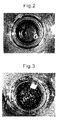
Fig. 2 is a photograph showing the foamed state of a Ti film-attached sample piece when dipped in the etching solution of Example 1. -
Fig. 3 is a photograph showing the foamed state of a Ti film-attached sample piece when dipped in the etching solution of Comparative Example 3. -
Fig. 4 is a graph showing the change in titanium/tungsten (TiW) etching rate with time for etching solutions having the compositions of Example 12 and Comparative Example 2. - The invention will now be explained in greater detail.
- The etching solution for titanium-based metals, tungsten-based metals, titanium/tungsten-based metals or their nitrides, according to the invention, comprises an aqueous solution containing hydrogen peroxide and an organic acid salt.
- The hydrogen peroxide is present in the etching solution at 10-40 mass%, more preferably 15-35 mass% and even more preferably 20-35 mass%. If the hydrogen peroxide concentration is lower than 10 mass%, the etching rate for titanium, tungsten or titanium/tungsten alloys will be reduced, making it impractical. If the hydrogen peroxide concentration is higher than 40 mass%, on the other hand, more hydrogen peroxide will decompose, likewise making it impractical.
- The organic acid salts useful for the invention are not particularly limited, but when an organic acid salt is used for production of an electronic device such as a semiconductor which is preferably void of metal impurities, it is more preferred to use an ammonium salt.
- The organic acid salt is present in the etching solution at 0.1-15 mass%, more preferably 1-10 masses% and even more preferably 3-8 mass%. If the organic acid salt concentration is lower than 0.1 mass%, the etching rate will be reduced, making it impractical. If the concentration is higher than 15 mass%, there will be no significant increase in the etching rate.
- The organic acid salt is not particularly restricted, and may be a salt on citric acid, formic acid, oxalic acid, acetic acid, tartaric acid, succinic acid, malic acid, maleic acid, malonic acid, glutaric acid, adipic acid, D-glucanic acid, itaconic acid, citraconic acid, mesaconic acid, 2-oxoglutaric acid, trimellitic acid, endothall, glutamic acid, result of evaluating etching properties for titanium-based metals, tungsten-based metals or their nitrides, the present inventors have found that neutral etching solutions rather than one tend to have higher etching rates. An organic acid salt is used for this reason. Salts of citric acid, formic acid, oxalic acid, acetic acid, tartaric acid and succinic acid are preferred, with diammonium hydrogen citrate, triammonium citrate, ammonium oxalate, ammonium any ammonium acetate being even more preferred. These may be used alone or in combinations of two or more. An organic acid ammonium salt may be used as the organic acid ammonium salt itself, or it may be used as the reaction product of the organic acid and ammonia in the etching solution, without any particular restrictions.
- Ammonia may be added as necessary to increase the etching rate of the titanium-based metal, tungsten-based metal, titanium/tungsten-based metal or its nitride. When ammonia is added, the concentration in the etching solution is in the range of 0.005-4.5 mass%, more preferably 0.05-2 mass% and even more preferably 0.1-0.5 mass%. If the ammonia concentration is higher than 4.5 mass%, the etching rate for titanium-based metals, tungsten-based metals or their nitrides will increase, but metals in the device that are prone to corrosion by alkalis, such as A1, will also be etched, and this is therefore undesirable.
- The etching solution of the invention having the composition described above has little foaming during etching of titanium-based metals, tungsten-based metals, titanium/tungsten-based metals or their nitrides, and it therefore allows uniform etching. The etching solution of the invention is superior in that it has a low etching rate for metals other than titanium-based metals, tungsten-based metals and titanium/tungsten-based metals, or base materials (glass, silicon, silicon oxide, silicon nitride), and the selective etching property for titanium-based metals, tungsten-based metals, titanium/tungsten-based metals or their nitrides (the ratio of the etching rate for titanium-based metals, tungsten-based metals or their nitrides with respect to the etching rate for metals other than titanium-based metals and tungsten-based metals or base materials (glass, silicon, silicon oxide, silicon nitride)) is at least 20. The etching solution of the invention may also contain components other than those mentioned above, such as moistening agents, surfactants, coloring agents, foam inhibitors and organic solvents, in ranges that do not affect the etching property.
- The term "titanium-based metal" as used herein means titanium metal (Ti), or an alloy comprising titanium as the main component (at
lease 70 mass%). A titanium-based metal nitride means a nitride of titanium metal or a titanium alloy, of which titanium nitride is a typical example. A specific example of a titanium alloy is titanium silicide (TiSi). Similarly, "tungsten-based metal" means tungsten metal (W) or an alloy comprising tungsten as the main component (at least 70 mass%). A nitride of a tungsten metal is a nitride of tungsten metal or a tungsten alloy, of which tungsten nitride is a typical example. Specific examples of tungsten alloys include molybdenum-tungsten (MoW) and tungsten silicide (MSi). - The term "titanium/tungsten-based metal" as used herein means an alloy including both titanium and tungsten, with a total of at least 70 mass% of both. A nitride of a titanium/tungsten-based metal is a nitride of such a titanium/tungsten alloy.
- The method of forming a film of the titanium-based metal, tungsten-based metal or titanium/tungsten-based metal on the substrate is not particularly restricted, and any method such as CVD, sputtering or vapor deposition may be used, while the film-forming conditions also are not restricted. A metal other than a titanium-based metal, tungsten-based metal or titanium/tungsten-based metal, as used herein, is Al, Ni, Cu, Cr, Ru, Ta, Si or an alloy comprising any of these elements as the main component (70 mass% or greater) (or a total of 70 mass% or greater when it contains more than one element), and it may contain the other elements.
- There are no particular restrictions on the device employing the titanium-based metal, tungsten-based metal, titanium/tungsten-based metal or its nitride, and it may be used in general electronic devices. An electronic device in this case is a liquid crystal display, semiconductor device, MEMS device, printed wiring board, organic EL display, field emission display, electronic paper, plasma display, or the like. The term "etching" as used herein refers to a process utilizing the etching phenomenon, and it naturally includes patterning of titanium-based metals, tungsten-based metals and titanium/tungsten-based metals, as well as purposes of cleaning off of titanium-based metal, tungsten-based metal or titanium/tungsten-based metal residues. Thus, the electronic device may further include electronic derices of which production process has a step of dissolving off of the entirety of the titanium-based metal, tungsten-based metal or titanium/tungsten-based metal by an etching solution, even if no titanium, tungsten or titanium/tungsten alloy remains on the final product.
- Treatment of a titanium-based metal, tungsten-based metal or titanium/tungsten-based metal, or a nitride thereof, with an etching solution according to the invention will usually be accomplished by a dipping method, but other methods such as spraying or spin etching may be used for the treatment. The conditions for treatment by dipping cannot be specified for all cases since they will differ depending on the hydrogen peroxide concentration, the organic acid ammonium salt type and content, and the film thickness of the titanium-based metal, tungsten-based metal, titanium/tungsten-based metal or nitride thereof, but, generally the treatment temperature will be 20-80°C and more preferably 30-60°C. Such treatment may also be carried out while applying ultrasonic waves.
- The present invention will now be explained in greater detail based on examples and comparative examples, with the understanding that the invention is not limited to these descriptions.
- Sample substrates having Ti, W and Al films formed by sputtering (film thickness: 50 nm each) of Ti, W or Al on a non-alkaline glass substrate for an LCD (liquid crystal display) were each cut to approximately 0.5 cm square to obtain sample pieces. In a 100 ml beaker there was loaded 20 ml of an etching solution having the composition of each of the examples and comparative examples listed in Table 1 below, and heating was performed to 50°C. One each of the Ti, W, Al film-attached sample pieces was simultaneously loaded into the etching solution, and the time until total disappearance of each sputtering film was visually observed. The same measurement was conducted 3 times, and the average values for the etching rates of Ti, W and Al were calculated. Table 1 summarizes the etching rates for each of the examples and comparative examples. The portion in addition to the constituent components of each etching solution shown in Table 1 is water (ultrapure water). The etching solutions of the examples and comparative examples were each prepared with their compositions, with ultrapure water as necessary, using a specially product of 35 mass% hydrogen peroxide water by Kishida Chemical Co., Ltd., EL grade 28 mass% ammonia water by Kanto Kagaku Co., Ltd., and a commercially available organic acid ammonium salt.
- Ni, Cu, Cr, Ru, Ta, Si film-attached sample pieces were used for measurement in the same manner as measurement of the Ti, W and Al etching rates, except that the sputtering film materials were changed from Ti, W and Al to Ni, Cu, Cr, Ru, Ta and Si, and the etching rates were calculated. Table 2 below shows the results of measurement using etching solutions having the compositions of Examples 1, 2 and 3.
- In a 100 ml beaker there was loaded 20 ml of an etching solution having the composition of Example 1 in Table 1, and heating was performed to 50°C. One Ti film-attached sample piece was loaded into the etching solution kept at 50°C. With the sample piece-loading point as the starting point (0 hours), one Ti film-attached sample piece was loaded every hour thereafter while keeping the temperature at 50°C, and the etching rate up to 6 hours thereafter was measured. The method of measuring the etching rate was the same as the method described above. As a comparative example, an experiment was conducted in the same manner using an etching solution comprising 30 mass% hydrogen peroxide, 0.3 mass% phosphoric acid, 0.02 mass% ammonia and 69.68 mass% ultrapure water (Comparative Example 3). The results are shown in
Fig. 1 . - An etching solution having the composition of Example 1 in Table 1 was prepared and kept at a constant temperature of 50°C. A 0.5 cm-square Ti film (50 nm thickness)-attached sample piece was dipped in the etching solution for 1 minute. The foaming condition of the solution at that time was recorded in a photograph. As a comparative example, the foaming condition was evaluated in the same manner using an etching solution comprising 30 mass% hydrogen peroxide, 0.3 mass% phosphoric acid, 0.02 mass% ammonia and 69.68 mass% ultrapure water (Comparative Example 3). The results are shown in
Figs. 2 and 3 . - In a 50 ml beaker there was loaded 20 ml of an etching solution having the composition or Example 12 in Table 1, and heating was performed to 45°C. One TiW film-attached silicon wafer piece (approximately 0.5 cm square, TiW film thickness: 200 nm) was loaded into the etching solution kept at 45°C. With the sample piece-loading point as the starting point (0 hours), one TiW film-attached sample piece was loaded every 6 hours thereafter while keeping the temperature at 45°C, and the etching rate was measured up to 66 hours thereafter. The method of measuring the etching rate was the same as the method described above. As a comparative example, an experiment was conducted in the same manner using an etching solution comprising 30 mass% hydrogen peroxide and 70 mass% ultrapure water (Comparative Example 2). The results are shown in
Fig. 4 . The TiW composition used was 10 mass% Ti, 90 mass% W.
Table 2 Cu Ni Ru Ta Cr Si SiO2 Si3N3 Example 1 <1.0 <1.0 <1.0 <1.0 <1.0 <1.0 <1.0 <1.0 Example 2 <1.0 <1.0 <1.0 <1.0 <1.0 <1.0 <1.0 <1.0 Example 3 <1.0 <1.0 <1.0 <1.0 <1.0 <1.0 <1.0 <1.0 - As shown in Table 1, the ratio of the etching rate tor Ti and W to the etching rate for A1, using etching solutions having the compositions of Examples 1-26, was 20 or higher, indicating an excellent selective etching property for Ti and W. The etching rate was generally satisfactory, at greater than 50 nm/min, although the Ti etching rate was somewhat lower with some of the compositions. On the other hand, all of the W etching rates were satisfactory at 150 nm/min or greater. In contrast, both the Ti and W etching rates were inadequately low at below 50 nm/min with the etching solution of Comparative Example 1. The Ti etching rate was also inadequately low at below 50 nm/min in Comparative Example 2.
- Table 2 shows that the etching solutions of the invention had low etching rates for Ni, Cu, Cr, Ru, Ta, Si, SiO2 and Si3N4 as for Al, and therefore had satisfactory selective etching properties for titanium and tungsten with respect to these as well. In addition,
Fig. 1 shows that the reduction in titanium etching rate with time was lower with the etching solutions of the invention, and therefore excellent stability was exhibited. With the etching solution of Comparative Example 3, on the other hand, the initial Ti etching rate (150 nm/min) was higher than the etching solution in Example 1, but the change (reduction) in the etching rate with time was large, and therefore the stability was inferior. - When the etching rates were measured for WN, TiW and TiN in the same manner as the composition of Example 1, they were found to be 320 nm/min, 200 nm/min and 120 nm/min, respectively. The TiW composition was 10 mass% and 90 mass% for Ti and W, respectively. The WN and TiN used had the compositions represented by their chemical formulas.
-
Figs. 2 and 3 show the foaming conditions of the etching solutions when a Ti film-attached sample piece was loaded into each etching solution. The photographs are taken from above the beaker. Considerable foaming of the etching solution is seen inFig. 3 (the etching solution of Comparative Example 3), but virtually none is seen inFig. 2 (the etching solution of Example 1). This demonstrated that an etching solution of the invention is advantageous for uniform etching of titanium-based metals, because it has little foaming during etching. -
Fig. 4 shows that the reduction in TiN etching rate with time was lower with the etching solutions of the invention, and therefore excellent stability was exhibited. With the etching solution of Comparative Example 2, on the other hand, the change (reduction) in the TiW etching rate (50 nm/min) with time was large, and therefore the stability was inferior. - By using an etching solution according to the invention it is possible to accomplish uniform etching of titanium, tungsten and alloys thereof, or their nitrides. In addition, an etching solution of the invention has a low etching rate for other metals such as copper, nickel and aluminum, and for glass, silicon and silicon oxide films, and is therefore useful for production of electronic devices such as semiconductor devices and liquid crystal displays, without damage to substrates and silicon oxide films.
Claims (8)
- An etching solution for titanium-based metals, tungsten-based metals, titanium/tungsten-based metals or their nitrides, which comprises 10-40 mass% hydrogen peroxide, 0.1-15 mass% of an organic acid salt, and water.
- An etching solution for titanium-based metals, tungsten-based metals, titanium/tungsten-based metals or their nitrides, which consists of 10-40 mass% hydrogen peroxide, 0.1-15 mass% of an organic acid salt, and water.
- An etching solution for titanium-based metals, tungsten-based metals, titanium/tungsten-based metals or their nitrides, according to claim 1, which further comprises 0.005-4.5 mass% ammonia.
- An etching solution for titanium-based metals, tungsten-based metals, titanium/tungsten-based metals or their nitrides, according to any one of claims 1 to 3, wherein the organic acid salt is at least one selected from among ammonium salts of citric acid, formic acid, oxalic acid, acetic acid, tartaric acid, benzole acid and succinic acid.
- An etching solution for titanium-based metals, tungsten-based metals, titanium/tungsten-based metals or their nitrides, according to claim 4, wherein the ammonium salt of an organic acid is ant least one selected from among diammonium hydrogen citrate, triammonium citrate, ammonium oxalate, ammonium formate and ammonium acetate.
- An etching solution for titanium-based metals, tungsten-based metals, titanium/tungsten-based metals or their nitrides, according to any one of claims 1 to 5, wherein the ratio of the etching rate for titanium-based metals or their nitrides to that for Al, Ni, Cu, Cr, Ru, Ta, Si or alloys composed mainly of these elements, is at least 20.
- An etching solution for titanium-based metals, tungsten-based metals, titanium/tungsten-based metals or their nitrides, according to any one of claims 1 to 5, wherein the ratio of the etching rate for titanium-based metals or their nitrides to that for glass, silicon, silicon oxide or silicon nitride, is at least 20.
- A method for producing an electronic device, which comprises a step of etching a titanium-based metal, tungsten-based metal, titanium/tungsten-based metal or a nitride thereof using an etching solution according to any one of claims 1 to 7.
Applications Claiming Priority (2)
| Application Number | Priority Date | Filing Date | Title |
|---|---|---|---|
| JP2008231325 | 2008-09-09 | ||
| PCT/JP2009/065136 WO2010029867A1 (en) | 2008-09-09 | 2009-08-25 | Etchant for titanium-based metal, tungsten-based metal, titanium-tungsten-based metal or nitrides thereof |
Publications (3)
| Publication Number | Publication Date |
|---|---|
| EP2322692A1 true EP2322692A1 (en) | 2011-05-18 |
| EP2322692A4 EP2322692A4 (en) | 2015-05-06 |
| EP2322692B1 EP2322692B1 (en) | 2016-10-12 |
Family
ID=42005124
Family Applications (1)
| Application Number | Title | Priority Date | Filing Date |
|---|---|---|---|
| EP09813013.1A Active EP2322692B1 (en) | 2008-09-09 | 2009-08-25 | Etchant for titanium-based metal, tungsten-based metal, titanium-tungsten-based metal or nitrides thereof |
Country Status (7)
| Country | Link |
|---|---|
| US (1) | US20110147341A1 (en) |
| EP (1) | EP2322692B1 (en) |
| JP (1) | JP5523325B2 (en) |
| KR (1) | KR101282177B1 (en) |
| CN (1) | CN102149851A (en) |
| TW (1) | TWI460310B (en) |
| WO (1) | WO2010029867A1 (en) |
Cited By (5)
| Publication number | Priority date | Publication date | Assignee | Title |
|---|---|---|---|---|
| WO2015054460A1 (en) * | 2013-10-11 | 2015-04-16 | E. I. Du Pont De Nemours And Company | Removal composition for selectively removing hard mask |
| EP2798669A4 (en) * | 2011-12-28 | 2015-08-19 | Entegris Inc | COMPOSITIONS AND METHODS FOR THE SELECTIVE ATTACK OF TITANIUM NITRIDE |
| CN105612599A (en) * | 2013-10-11 | 2016-05-25 | E.I.内穆尔杜邦公司 | Removal composition for selectively removing hard mask |
| DE102015121233A1 (en) * | 2015-12-07 | 2017-06-08 | Biotronik Se & Co. Kg | Method for treating a metallic workpiece |
| EP4098771A4 (en) * | 2020-01-30 | 2023-06-14 | Resonac Corporation | METAL COMPOUND REMOVAL PROCESS |
Families Citing this family (30)
| Publication number | Priority date | Publication date | Assignee | Title |
|---|---|---|---|---|
| KR101708290B1 (en) * | 2010-08-02 | 2017-03-09 | 에스케이하이닉스 주식회사 | Method for fabricating semiconductor device |
| US9831088B2 (en) * | 2010-10-06 | 2017-11-28 | Entegris, Inc. | Composition and process for selectively etching metal nitrides |
| US8940597B2 (en) | 2013-03-11 | 2015-01-27 | Taiwan Semiconductor Manufacturing Co., Ltd. | In-situ metal gate recess process for self-aligned contact application |
| WO2014168037A1 (en) | 2013-04-12 | 2014-10-16 | 三菱瓦斯化学株式会社 | Liquid composition used in etching copper- and titanium-containing multilayer film, etching method in which said composition is used, method for manufacturing multilayer-film wiring, and substrate |
| KR102340516B1 (en) * | 2013-08-30 | 2021-12-21 | 엔테그리스, 아이엔씨. | Compositions and methods for selectively etching titanium nitride |
| KR102088840B1 (en) * | 2013-09-10 | 2020-04-16 | 동우 화인켐 주식회사 | ETCHANT COMPOSITION FOR NICKEL-BASED METAL LAYER AND TiN |
| US20150368557A1 (en) | 2014-06-23 | 2015-12-24 | Hyosan Lee | Metal etchant compositions and methods of fabricating a semiconductor device using the same |
| KR101587758B1 (en) | 2015-03-05 | 2016-01-21 | 동우 화인켐 주식회사 | ETCHANT COMPOSITION FOR ETHCING TiN LAYER AND METHOD FOR FORMING METAL LINE USING THE SAME |
| KR20160111649A (en) | 2015-03-17 | 2016-09-27 | 동우 화인켐 주식회사 | Etching composition for a metal |
| KR20160111650A (en) | 2015-03-17 | 2016-09-27 | 동우 화인켐 주식회사 | Non-aqueous etching composition for a metal |
| US9976111B2 (en) | 2015-05-01 | 2018-05-22 | Versum Materials Us, Llc | TiN hard mask and etch residual removal |
| US9524935B2 (en) | 2015-05-13 | 2016-12-20 | Globalfoundries Inc. | Filling cavities in an integrated circuit and resulting devices |
| CN104962921B (en) * | 2015-05-22 | 2017-06-27 | 江苏大学 | A kind of preparation method of nickel-titanium alloy surface nickel-free layer |
| CN104911595B (en) * | 2015-06-23 | 2018-02-09 | 西安空间无线电技术研究所 | A kind of TiW film layers caustic solution |
| KR102487249B1 (en) | 2015-12-11 | 2023-01-13 | 동우 화인켐 주식회사 | Etching solution composition for a tungsten layer |
| US10538846B2 (en) | 2015-12-11 | 2020-01-21 | Dongwoo Fine-Chem Co., Ltd. | Etching solution composition for tungsten layer, method for preparing electronic device using the same and electronic device |
| KR102415954B1 (en) | 2016-01-12 | 2022-07-01 | 동우 화인켐 주식회사 | ETCHANT COMPOSITION FOR ETHCING TiN LAYER AND METHOD FOR FORMING METAL LINE USING THE SAME |
| EP3436621B1 (en) * | 2016-03-29 | 2020-02-12 | Technic France | Solution and method for etching titanium based materials |
| KR102700158B1 (en) * | 2016-10-25 | 2024-08-28 | 동우 화인켐 주식회사 | Etchant composition for titanium nitride layer |
| TWI641725B (en) * | 2016-11-15 | 2018-11-21 | 添鴻科技股份有限公司 | Etching solution for titanium-tungsten alloy |
| US11035044B2 (en) | 2017-01-23 | 2021-06-15 | Versum Materials Us, Llc | Etching solution for tungsten and GST films |
| CN110462799B (en) | 2017-03-31 | 2023-12-26 | 关东化学株式会社 | Etching liquid composition and etching method for titanium layer or titanium-containing layer |
| WO2019054294A1 (en) * | 2017-09-12 | 2019-03-21 | 株式会社 東芝 | Method for manufacturing ceramic circuit board |
| JP6798045B2 (en) | 2018-01-16 | 2020-12-09 | 株式会社トクヤマ | Processing liquid for semiconductor wafers containing hypochlorite ions |
| US10818557B2 (en) | 2018-07-03 | 2020-10-27 | Globalfoundries Inc. | Integrated circuit structure to reduce soft-fail incidence and method of forming same |
| KR102309758B1 (en) * | 2019-03-25 | 2021-10-06 | 에스케이머티리얼즈 주식회사 | Compostion for etching titanium nitrate layer-tungsten layer containing laminate and methold for etching a semiconductor device using the same |
| KR102877724B1 (en) * | 2020-02-05 | 2025-10-29 | 삼성전자주식회사 | Etching composition and method for manufacturing semiconductor device using the same |
| KR102788291B1 (en) | 2020-03-16 | 2025-03-27 | 동우 화인켐 주식회사 | Composition for Etching Cobalt Layer |
| US20230420265A1 (en) * | 2022-06-22 | 2023-12-28 | Taiwan Semiconductor Manufacturing Company, Ltd. | Anisotropic wet etching in patterning |
| CN116180059B (en) * | 2023-04-28 | 2024-03-19 | 中国电子科技集团公司第十四研究所 | An HTCC substrate electroless plating rack and a method of using it for electroless plating |
Family Cites Families (12)
| Publication number | Priority date | Publication date | Assignee | Title |
|---|---|---|---|---|
| US4554050A (en) * | 1984-07-16 | 1985-11-19 | At&T Bell Laboratories | Etching of titanium |
| NL8701184A (en) * | 1987-05-18 | 1988-12-16 | Philips Nv | METHOD FOR MANUFACTURING A SEMICONDUCTOR DEVICE |
| DE4110595C1 (en) * | 1991-04-02 | 1992-11-26 | Thyssen Edelstahlwerke Ag, 4000 Duesseldorf, De | Wet-chemical removal of hard coatings from workpiece surfaces - comprises using hydrogen peroxide soln. stabilised by complex former e.g. potassium-sodium tartrate-tetra:hydrate |
| JPH06310492A (en) * | 1993-04-23 | 1994-11-04 | Fuji Xerox Co Ltd | Titanium-based thin film etching solution and method for manufacturing semiconductor device |
| US5462638A (en) * | 1994-06-15 | 1995-10-31 | International Business Machines Corporation | Selective etching of TiW for C4 fabrication |
| US5759437A (en) * | 1996-10-31 | 1998-06-02 | International Business Machines Corporation | Etching of Ti-W for C4 rework |
| JP3515076B2 (en) * | 2001-01-22 | 2004-04-05 | トヨタ自動車株式会社 | Release agent for Ti-based coating on super-hard material surface, release method and regeneration process for super-hard material |
| CN1465746A (en) * | 2002-06-25 | 2004-01-07 | 铼宝科技股份有限公司 | Silver alloy etching solution |
| JP4535232B2 (en) * | 2003-11-17 | 2010-09-01 | 三菱瓦斯化学株式会社 | Titanium or titanium alloy etchant |
| JP4474914B2 (en) * | 2003-12-17 | 2010-06-09 | 東ソー株式会社 | Resist residue stripping composition and cleaning method using the same |
| EP1866957A1 (en) * | 2005-04-08 | 2007-12-19 | Sachem, Inc. | Selective wet etching of metal nitrides |
| US20070203041A1 (en) * | 2006-02-24 | 2007-08-30 | Ki-Jeong Lee | Cleaning composition for removing impurities and method of removing impurities using the same |
-
2009
- 2009-08-25 WO PCT/JP2009/065136 patent/WO2010029867A1/en not_active Ceased
- 2009-08-25 KR KR1020117003351A patent/KR101282177B1/en not_active Expired - Fee Related
- 2009-08-25 CN CN2009801350620A patent/CN102149851A/en active Pending
- 2009-08-25 EP EP09813013.1A patent/EP2322692B1/en active Active
- 2009-08-25 US US13/060,406 patent/US20110147341A1/en not_active Abandoned
- 2009-08-25 JP JP2010528706A patent/JP5523325B2/en not_active Expired - Fee Related
- 2009-08-27 TW TW098128864A patent/TWI460310B/en active
Non-Patent Citations (1)
| Title |
|---|
| See references of WO2010029867A1 * |
Cited By (14)
| Publication number | Priority date | Publication date | Assignee | Title |
|---|---|---|---|---|
| EP2798669A4 (en) * | 2011-12-28 | 2015-08-19 | Entegris Inc | COMPOSITIONS AND METHODS FOR THE SELECTIVE ATTACK OF TITANIUM NITRIDE |
| US9546321B2 (en) | 2011-12-28 | 2017-01-17 | Advanced Technology Materials, Inc. | Compositions and methods for selectively etching titanium nitride |
| CN105612599A (en) * | 2013-10-11 | 2016-05-25 | E.I.内穆尔杜邦公司 | Removal composition for selectively removing hard mask |
| WO2015054460A1 (en) * | 2013-10-11 | 2015-04-16 | E. I. Du Pont De Nemours And Company | Removal composition for selectively removing hard mask |
| CN105874562A (en) * | 2013-10-11 | 2016-08-17 | E.I.内穆尔杜邦公司 | Removal composition for selectively removing hard mask and methods thereof |
| CN105874568A (en) * | 2013-10-11 | 2016-08-17 | Ekc技术公司 | Method and composition for selectively removing metal hardmask and other residues from semiconductor device substrates comprising low-k dielectric material and copper |
| WO2015054464A1 (en) * | 2013-10-11 | 2015-04-16 | E. I. Du Pont De Nemours And Company | Removal composition for selectively removing hard mask and methods thereof |
| US10005991B2 (en) | 2013-10-11 | 2018-06-26 | Ekc Technology Inc | Removal composition for selectively removing hard mask and methods thereof |
| US10155921B2 (en) | 2013-10-11 | 2018-12-18 | E I Dupont Ne Nemours And Company | Removal composition for selectively removing hard mask and methods thereof |
| CN105612599B (en) * | 2013-10-11 | 2019-05-14 | Ekc技术公司 | Removal composition for selective hard mask removal |
| CN105874562B (en) * | 2013-10-11 | 2019-05-14 | Ekc技术公司 | Removal compositions and methods for selectively removing hard masks |
| DE102015121233A1 (en) * | 2015-12-07 | 2017-06-08 | Biotronik Se & Co. Kg | Method for treating a metallic workpiece |
| EP4098771A4 (en) * | 2020-01-30 | 2023-06-14 | Resonac Corporation | METAL COMPOUND REMOVAL PROCESS |
| US12448567B2 (en) | 2020-01-30 | 2025-10-21 | Resonac Corporation | Method for removing metal compound |
Also Published As
| Publication number | Publication date |
|---|---|
| EP2322692A4 (en) | 2015-05-06 |
| TW201014927A (en) | 2010-04-16 |
| JP5523325B2 (en) | 2014-06-18 |
| WO2010029867A1 (en) | 2010-03-18 |
| JPWO2010029867A1 (en) | 2012-02-02 |
| KR101282177B1 (en) | 2013-07-04 |
| TWI460310B (en) | 2014-11-11 |
| CN102149851A (en) | 2011-08-10 |
| US20110147341A1 (en) | 2011-06-23 |
| KR20110031233A (en) | 2011-03-24 |
| EP2322692B1 (en) | 2016-10-12 |
Similar Documents
| Publication | Publication Date | Title |
|---|---|---|
| EP2322692B1 (en) | Etchant for titanium-based metal, tungsten-based metal, titanium-tungsten-based metal or nitrides thereof | |
| JP6960477B2 (en) | Chemical solution, manufacturing method of chemical solution, processing method of substrate | |
| EP2514855A1 (en) | Composition for etching ruthenium-based metal and method for preparing same | |
| KR101803209B1 (en) | Etchant composition and manufacturing method of an array for display | |
| CN101199043B (en) | Etchant composition and method for manufacturing semiconductor device using the same | |
| KR20080015027A (en) | Compositions and methods for the selective removal of metals or metal alloys after metal silicide formation | |
| JP6670917B1 (en) | An etching solution, a method for processing a target object, and a method for manufacturing a semiconductor element. | |
| EP3436621B1 (en) | Solution and method for etching titanium based materials | |
| KR20060039447A (en) | Etching solution for titanium containing layer and etching method of titanium containing layer | |
| JP6425342B2 (en) | Etching solution, etching method using the same, and method of manufacturing semiconductor substrate product | |
| CN100516303C (en) | Removing liquid for tungsten metal and method for removing tungsten metal using such liquid | |
| JP5960099B2 (en) | Etching method, semiconductor substrate product using the same, and semiconductor device manufacturing method | |
| JP2014146623A (en) | Method of etching semiconductor substrate, etchant, and method of manufacturing semiconductor element | |
| KR102179756B1 (en) | Etching solution composition for a metal nitride layer | |
| KR20160112470A (en) | Etchant composition and manufacturing method of an array for liquid crystal display | |
| KR102412268B1 (en) | Manufacturing method of an array substrate for crystal display | |
| JP6369989B2 (en) | Etching solution, etching method, and method for manufacturing semiconductor substrate product | |
| KR102603630B1 (en) | Manufacturing method of an array substrate for a display divice | |
| KR102487249B1 (en) | Etching solution composition for a tungsten layer | |
| KR20160090574A (en) | Etching solution composition for copper-based metal layer and method for etching copper-based metal layer using the same | |
| CN107653451B (en) | Etching solution composition and method for manufacturing metal pattern using the same | |
| KR20130049505A (en) | Etching solution composition for a tungsten layer and method for etching the tungsten layer using the same | |
| KR20160112929A (en) | Etchant composition and manufacturing method of an array for liquid crystal display | |
| KR20170022097A (en) | ETCHANT COMPOSITION FOR ETHCING TiN LAYER AND METHOD FOR FORMING METAL LINE USING THE SAME | |
| KR20200111361A (en) | COMPOSITION FOR REMOVAL OF TiOx RESIDUE |
Legal Events
| Date | Code | Title | Description |
|---|---|---|---|
| PUAI | Public reference made under article 153(3) epc to a published international application that has entered the european phase |
Free format text: ORIGINAL CODE: 0009012 |
|
| 17P | Request for examination filed |
Effective date: 20110405 |
|
| AK | Designated contracting states |
Kind code of ref document: A1 Designated state(s): AT BE BG CH CY CZ DE DK EE ES FI FR GB GR HR HU IE IS IT LI LT LU LV MC MK MT NL NO PL PT RO SE SI SK SM TR |
|
| AX | Request for extension of the european patent |
Extension state: AL BA RS |
|
| DAX | Request for extension of the european patent (deleted) | ||
| RA4 | Supplementary search report drawn up and despatched (corrected) |
Effective date: 20150402 |
|
| RIC1 | Information provided on ipc code assigned before grant |
Ipc: C23G 1/20 20060101ALI20150327BHEP Ipc: C23F 1/38 20060101AFI20150327BHEP Ipc: C11D 11/00 20060101ALI20150327BHEP Ipc: C23F 1/44 20060101ALI20150327BHEP |
|
| 17Q | First examination report despatched |
Effective date: 20151117 |
|
| GRAP | Despatch of communication of intention to grant a patent |
Free format text: ORIGINAL CODE: EPIDOSNIGR1 |
|
| INTG | Intention to grant announced |
Effective date: 20160331 |
|
| GRAJ | Information related to disapproval of communication of intention to grant by the applicant or resumption of examination proceedings by the epo deleted |
Free format text: ORIGINAL CODE: EPIDOSDIGR1 |
|
| GRAP | Despatch of communication of intention to grant a patent |
Free format text: ORIGINAL CODE: EPIDOSNIGR1 |
|
| GRAS | Grant fee paid |
Free format text: ORIGINAL CODE: EPIDOSNIGR3 |
|
| INTC | Intention to grant announced (deleted) | ||
| INTG | Intention to grant announced |
Effective date: 20160810 |
|
| GRAA | (expected) grant |
Free format text: ORIGINAL CODE: 0009210 |
|
| AK | Designated contracting states |
Kind code of ref document: B1 Designated state(s): AT BE BG CH CY CZ DE DK EE ES FI FR GB GR HR HU IE IS IT LI LT LU LV MC MK MT NL NO PL PT RO SE SI SK SM TR |
|
| REG | Reference to a national code |
Ref country code: GB Ref legal event code: FG4D |
|
| REG | Reference to a national code |
Ref country code: CH Ref legal event code: EP |
|
| REG | Reference to a national code |
Ref country code: AT Ref legal event code: REF Ref document number: 836588 Country of ref document: AT Kind code of ref document: T Effective date: 20161015 |
|
| REG | Reference to a national code |
Ref country code: IE Ref legal event code: FG4D |
|
| REG | Reference to a national code |
Ref country code: DE Ref legal event code: R096 Ref document number: 602009041739 Country of ref document: DE |
|
| REG | Reference to a national code |
Ref country code: LT Ref legal event code: MG4D |
|
| REG | Reference to a national code |
Ref country code: NL Ref legal event code: MP Effective date: 20161012 |
|
| PG25 | Lapsed in a contracting state [announced via postgrant information from national office to epo] |
Ref country code: LV Free format text: LAPSE BECAUSE OF FAILURE TO SUBMIT A TRANSLATION OF THE DESCRIPTION OR TO PAY THE FEE WITHIN THE PRESCRIBED TIME-LIMIT Effective date: 20161012 |
|
| REG | Reference to a national code |
Ref country code: AT Ref legal event code: MK05 Ref document number: 836588 Country of ref document: AT Kind code of ref document: T Effective date: 20161012 |
|
| PG25 | Lapsed in a contracting state [announced via postgrant information from national office to epo] |
Ref country code: GR Free format text: LAPSE BECAUSE OF FAILURE TO SUBMIT A TRANSLATION OF THE DESCRIPTION OR TO PAY THE FEE WITHIN THE PRESCRIBED TIME-LIMIT Effective date: 20170113 Ref country code: LT Free format text: LAPSE BECAUSE OF FAILURE TO SUBMIT A TRANSLATION OF THE DESCRIPTION OR TO PAY THE FEE WITHIN THE PRESCRIBED TIME-LIMIT Effective date: 20161012 Ref country code: NO Free format text: LAPSE BECAUSE OF FAILURE TO SUBMIT A TRANSLATION OF THE DESCRIPTION OR TO PAY THE FEE WITHIN THE PRESCRIBED TIME-LIMIT Effective date: 20170112 Ref country code: SE Free format text: LAPSE BECAUSE OF FAILURE TO SUBMIT A TRANSLATION OF THE DESCRIPTION OR TO PAY THE FEE WITHIN THE PRESCRIBED TIME-LIMIT Effective date: 20161012 |
|
| PG25 | Lapsed in a contracting state [announced via postgrant information from national office to epo] |
Ref country code: HR Free format text: LAPSE BECAUSE OF FAILURE TO SUBMIT A TRANSLATION OF THE DESCRIPTION OR TO PAY THE FEE WITHIN THE PRESCRIBED TIME-LIMIT Effective date: 20161012 Ref country code: ES Free format text: LAPSE BECAUSE OF FAILURE TO SUBMIT A TRANSLATION OF THE DESCRIPTION OR TO PAY THE FEE WITHIN THE PRESCRIBED TIME-LIMIT Effective date: 20161012 Ref country code: FI Free format text: LAPSE BECAUSE OF FAILURE TO SUBMIT A TRANSLATION OF THE DESCRIPTION OR TO PAY THE FEE WITHIN THE PRESCRIBED TIME-LIMIT Effective date: 20161012 Ref country code: PT Free format text: LAPSE BECAUSE OF FAILURE TO SUBMIT A TRANSLATION OF THE DESCRIPTION OR TO PAY THE FEE WITHIN THE PRESCRIBED TIME-LIMIT Effective date: 20170213 Ref country code: AT Free format text: LAPSE BECAUSE OF FAILURE TO SUBMIT A TRANSLATION OF THE DESCRIPTION OR TO PAY THE FEE WITHIN THE PRESCRIBED TIME-LIMIT Effective date: 20161012 Ref country code: BE Free format text: LAPSE BECAUSE OF FAILURE TO SUBMIT A TRANSLATION OF THE DESCRIPTION OR TO PAY THE FEE WITHIN THE PRESCRIBED TIME-LIMIT Effective date: 20161012 Ref country code: IS Free format text: LAPSE BECAUSE OF FAILURE TO SUBMIT A TRANSLATION OF THE DESCRIPTION OR TO PAY THE FEE WITHIN THE PRESCRIBED TIME-LIMIT Effective date: 20170212 Ref country code: NL Free format text: LAPSE BECAUSE OF FAILURE TO SUBMIT A TRANSLATION OF THE DESCRIPTION OR TO PAY THE FEE WITHIN THE PRESCRIBED TIME-LIMIT Effective date: 20161012 Ref country code: PL Free format text: LAPSE BECAUSE OF FAILURE TO SUBMIT A TRANSLATION OF THE DESCRIPTION OR TO PAY THE FEE WITHIN THE PRESCRIBED TIME-LIMIT Effective date: 20161012 |
|
| REG | Reference to a national code |
Ref country code: DE Ref legal event code: R097 Ref document number: 602009041739 Country of ref document: DE |
|
| REG | Reference to a national code |
Ref country code: FR Ref legal event code: PLFP Year of fee payment: 9 |
|
| PG25 | Lapsed in a contracting state [announced via postgrant information from national office to epo] |
Ref country code: SK Free format text: LAPSE BECAUSE OF FAILURE TO SUBMIT A TRANSLATION OF THE DESCRIPTION OR TO PAY THE FEE WITHIN THE PRESCRIBED TIME-LIMIT Effective date: 20161012 Ref country code: RO Free format text: LAPSE BECAUSE OF FAILURE TO SUBMIT A TRANSLATION OF THE DESCRIPTION OR TO PAY THE FEE WITHIN THE PRESCRIBED TIME-LIMIT Effective date: 20161012 Ref country code: DK Free format text: LAPSE BECAUSE OF FAILURE TO SUBMIT A TRANSLATION OF THE DESCRIPTION OR TO PAY THE FEE WITHIN THE PRESCRIBED TIME-LIMIT Effective date: 20161012 Ref country code: CZ Free format text: LAPSE BECAUSE OF FAILURE TO SUBMIT A TRANSLATION OF THE DESCRIPTION OR TO PAY THE FEE WITHIN THE PRESCRIBED TIME-LIMIT Effective date: 20161012 Ref country code: EE Free format text: LAPSE BECAUSE OF FAILURE TO SUBMIT A TRANSLATION OF THE DESCRIPTION OR TO PAY THE FEE WITHIN THE PRESCRIBED TIME-LIMIT Effective date: 20161012 |
|
| PLBE | No opposition filed within time limit |
Free format text: ORIGINAL CODE: 0009261 |
|
| STAA | Information on the status of an ep patent application or granted ep patent |
Free format text: STATUS: NO OPPOSITION FILED WITHIN TIME LIMIT |
|
| PG25 | Lapsed in a contracting state [announced via postgrant information from national office to epo] |
Ref country code: SM Free format text: LAPSE BECAUSE OF FAILURE TO SUBMIT A TRANSLATION OF THE DESCRIPTION OR TO PAY THE FEE WITHIN THE PRESCRIBED TIME-LIMIT Effective date: 20161012 Ref country code: BG Free format text: LAPSE BECAUSE OF FAILURE TO SUBMIT A TRANSLATION OF THE DESCRIPTION OR TO PAY THE FEE WITHIN THE PRESCRIBED TIME-LIMIT Effective date: 20170112 Ref country code: IT Free format text: LAPSE BECAUSE OF FAILURE TO SUBMIT A TRANSLATION OF THE DESCRIPTION OR TO PAY THE FEE WITHIN THE PRESCRIBED TIME-LIMIT Effective date: 20161012 |
|
| 26N | No opposition filed |
Effective date: 20170713 |
|
| PG25 | Lapsed in a contracting state [announced via postgrant information from national office to epo] |
Ref country code: SI Free format text: LAPSE BECAUSE OF FAILURE TO SUBMIT A TRANSLATION OF THE DESCRIPTION OR TO PAY THE FEE WITHIN THE PRESCRIBED TIME-LIMIT Effective date: 20161012 |
|
| REG | Reference to a national code |
Ref country code: CH Ref legal event code: PL |
|
| PG25 | Lapsed in a contracting state [announced via postgrant information from national office to epo] |
Ref country code: MC Free format text: LAPSE BECAUSE OF FAILURE TO SUBMIT A TRANSLATION OF THE DESCRIPTION OR TO PAY THE FEE WITHIN THE PRESCRIBED TIME-LIMIT Effective date: 20161012 |
|
| PG25 | Lapsed in a contracting state [announced via postgrant information from national office to epo] |
Ref country code: CH Free format text: LAPSE BECAUSE OF NON-PAYMENT OF DUE FEES Effective date: 20170831 Ref country code: LI Free format text: LAPSE BECAUSE OF NON-PAYMENT OF DUE FEES Effective date: 20170831 |
|
| REG | Reference to a national code |
Ref country code: IE Ref legal event code: MM4A |
|
| PG25 | Lapsed in a contracting state [announced via postgrant information from national office to epo] |
Ref country code: LU Free format text: LAPSE BECAUSE OF NON-PAYMENT OF DUE FEES Effective date: 20170825 |
|
| REG | Reference to a national code |
Ref country code: FR Ref legal event code: PLFP Year of fee payment: 10 |
|
| PG25 | Lapsed in a contracting state [announced via postgrant information from national office to epo] |
Ref country code: IE Free format text: LAPSE BECAUSE OF NON-PAYMENT OF DUE FEES Effective date: 20170825 |
|
| PG25 | Lapsed in a contracting state [announced via postgrant information from national office to epo] |
Ref country code: MT Free format text: LAPSE BECAUSE OF NON-PAYMENT OF DUE FEES Effective date: 20170825 |
|
| PG25 | Lapsed in a contracting state [announced via postgrant information from national office to epo] |
Ref country code: HU Free format text: LAPSE BECAUSE OF FAILURE TO SUBMIT A TRANSLATION OF THE DESCRIPTION OR TO PAY THE FEE WITHIN THE PRESCRIBED TIME-LIMIT; INVALID AB INITIO Effective date: 20090825 |
|
| PG25 | Lapsed in a contracting state [announced via postgrant information from national office to epo] |
Ref country code: CY Free format text: LAPSE BECAUSE OF NON-PAYMENT OF DUE FEES Effective date: 20161012 |
|
| PG25 | Lapsed in a contracting state [announced via postgrant information from national office to epo] |
Ref country code: MK Free format text: LAPSE BECAUSE OF FAILURE TO SUBMIT A TRANSLATION OF THE DESCRIPTION OR TO PAY THE FEE WITHIN THE PRESCRIBED TIME-LIMIT Effective date: 20161012 |
|
| PG25 | Lapsed in a contracting state [announced via postgrant information from national office to epo] |
Ref country code: TR Free format text: LAPSE BECAUSE OF FAILURE TO SUBMIT A TRANSLATION OF THE DESCRIPTION OR TO PAY THE FEE WITHIN THE PRESCRIBED TIME-LIMIT Effective date: 20161012 |
|
| REG | Reference to a national code |
Ref country code: DE Ref legal event code: R081 Ref document number: 602009041739 Country of ref document: DE Owner name: RESONAC CORP., JP Free format text: FORMER OWNER: SHOWA DENKO K.K., TOKYO, JP |
|
| PGFP | Annual fee paid to national office [announced via postgrant information from national office to epo] |
Ref country code: DE Payment date: 20240702 Year of fee payment: 16 |
|
| PGFP | Annual fee paid to national office [announced via postgrant information from national office to epo] |
Ref country code: GB Payment date: 20240701 Year of fee payment: 16 |
|
| PGFP | Annual fee paid to national office [announced via postgrant information from national office to epo] |
Ref country code: FR Payment date: 20240702 Year of fee payment: 16 |
|
| REG | Reference to a national code |
Ref country code: DE Ref legal event code: R119 Ref document number: 602009041739 Country of ref document: DE |
|
| GBPC | Gb: european patent ceased through non-payment of renewal fee |
Effective date: 20250825 |