EP2322395A1 - Infrared photocurrent front-end ADC for rain-sensing system with ambient light compensation - Google Patents
Infrared photocurrent front-end ADC for rain-sensing system with ambient light compensation Download PDFInfo
- Publication number
- EP2322395A1 EP2322395A1 EP20100368019 EP10368019A EP2322395A1 EP 2322395 A1 EP2322395 A1 EP 2322395A1 EP 20100368019 EP20100368019 EP 20100368019 EP 10368019 A EP10368019 A EP 10368019A EP 2322395 A1 EP2322395 A1 EP 2322395A1
- Authority
- EP
- European Patent Office
- Prior art keywords
- current
- ambient light
- digital
- compensation
- analog
- Prior art date
- Legal status (The legal status is an assumption and is not a legal conclusion. Google has not performed a legal analysis and makes no representation as to the accuracy of the status listed.)
- Granted
Links
Images




Classifications
-
- G—PHYSICS
- G01—MEASURING; TESTING
- G01S—RADIO DIRECTION-FINDING; RADIO NAVIGATION; DETERMINING DISTANCE OR VELOCITY BY USE OF RADIO WAVES; LOCATING OR PRESENCE-DETECTING BY USE OF THE REFLECTION OR RERADIATION OF RADIO WAVES; ANALOGOUS ARRANGEMENTS USING OTHER WAVES
- G01S7/00—Details of systems according to groups G01S13/00, G01S15/00, G01S17/00
- G01S7/48—Details of systems according to groups G01S13/00, G01S15/00, G01S17/00 of systems according to group G01S17/00
- G01S7/483—Details of pulse systems
- G01S7/486—Receivers
- G01S7/4868—Controlling received signal intensity or exposure of sensor
-
- B—PERFORMING OPERATIONS; TRANSPORTING
- B60—VEHICLES IN GENERAL
- B60S—SERVICING, CLEANING, REPAIRING, SUPPORTING, LIFTING, OR MANOEUVRING OF VEHICLES, NOT OTHERWISE PROVIDED FOR
- B60S1/00—Cleaning of vehicles
- B60S1/02—Cleaning windscreens, windows or optical devices
- B60S1/04—Wipers or the like, e.g. scrapers
- B60S1/06—Wipers or the like, e.g. scrapers characterised by the drive
- B60S1/08—Wipers or the like, e.g. scrapers characterised by the drive electrically driven
- B60S1/0818—Wipers or the like, e.g. scrapers characterised by the drive electrically driven including control systems responsive to external conditions, e.g. by detection of moisture, dirt or the like
- B60S1/0822—Wipers or the like, e.g. scrapers characterised by the drive electrically driven including control systems responsive to external conditions, e.g. by detection of moisture, dirt or the like characterized by the arrangement or type of detection means
- B60S1/0833—Optical rain sensor
Definitions
- This invention relates generally to a front-end circuit of an electro-optical sensing device and relates more specifically to accommodate an infrared pulse of a light receiving diode (LRD), receiving transmitted light from a light source, in presence of ambient current (ambient light in an LRD) for a rain-sensing system.
- LRD light receiving diode
- This performs measurements of the attenuation of reflected infrared LED light due to increased scattering of light by rain.
- infrared senders and receivers The usage of infrared senders and receivers is getting more and more popular and is known for numerous different applications and includes a transmitter (such as an infrared light emitting diode (LED)), which transmits light in the infrared range, and an optical receiver (phototransistor or photodiode or photo resistor), which converts the optical infrared signal into a proportional electrical signal.
- a transmitter such as an infrared light emitting diode (LED)
- LED infrared light emitting diode
- optical receiver phototransistor or photodiode or photo resistor
- U. S. Patent ( US 7,019,321 to Kokuryo et al ) proposes a rain sensing device that can estimate the size of raindrops or the like without a large amount of hardware resources, and its sensing method, and a wiper controlling apparatus using the same.
- a sensing device light emitted from a light-emitting member is introduced to a transparent plate, reflected by a sensing surface of the transparent plate and then received by a photo-detector, thereby detecting a condition of the sensing surface.
- U. S. Patent Publication US 2009/0121889 to Lin et al. discloses a proximity sensor including a driver, a photo-diode (PD) and an analog-to-digital converter (ADC).
- the proximity sensor can also include a controller to control the driver.
- the driver selectively drives a light source, e.g., an infrared (IR) light emitting diode (LED).
- IR infrared
- the PD which produces a current signal indicative of the intensity of light detected by the PD, is capable of detecting both ambient light and light produced by the light source that is reflected off an object.
- the ADC receives one or more portion of the current signal produced by the PD.
- U. S. Patent US 5,929,982 to Anderson ) describes an active avalanche photo-diode (APD) and a gain control circuit for use in an optical receiver including a bias generator for varying the bias on a variable gain APD in response to bias control values generated by a controller.
- the controller receives the output of the optical receiver and determines the system noise of the receiver for the various bias control values. The system noise is compared to a threshold value for establishing the optimum bias for optimum gain of the APD.
- the gain control circuit is useable in an optical receiver in an optical time domain reflectometer (OTDR) for increasing the dynamic range of the OTDR.
- the optical receiver includes an amplifier section for amplifying the output of the APD and an analog-to-digital converter for receiving and converting the amplified output of the amplifier section to digital values representative of an optical input received at the APD.
- a principal object of the present invention is to accommodate a current generated by a photo diode receiving a signal light from a LED in presence of ambient light to a front-end sensor system
- a further object of the invention is to accommodate a current generated by a photo diode receiving a signal light from an infrared LED in presence of ambient light to a front-end circuit of a rain-sensing system.
- a further object of the invention is to achieve a front-end circuit having a high dynamic range.
- a further object of the invention is to achieve a readout circuit with a high signal-to-noise ratio
- a further object of the invention is to maximize an infrared to ambient light ratio.
- a further object of the invention is to increase a front end ADC resolution to 14 bits.
- an object of the invention is to achieve a dynamic range of 160 dB of the infrared photocurrents.
- a method to accommodate a photodiode current generated by a signal light from a light source in presence of ambient light comprises, firstly, the steps of: (1) providing a light receiving photo diode receiving a signal light pulse from a light source and a front end system comprising a continuous-time programmable transresistance amplifier converting input current through multi-scaled feedback resistors into a voltage, a digital unit, an analog-to digital converter and a digital-to-analog converter, (2) calibrating said front end system by digitally correcting each raw output of the analog-to-digital converter while the photo diode is disconnected, and (3) extracting offset for ambient light compensation. Furthermore the method invented comprises the steps of (4) accommodating the ambient light compensation, (5) accommodating compensated ambient light and signal light pulse, (6) go back to step (2) if system is ON, otherwise go to step (7), and (7) end.
- a system to accommodate a photo diode current receiving a signal light of a sensor application in presence of ambient light having a high dynamic range comprises, firstly: said photo diode, receiving a signal light and ambient light, generating an output current; and a front-end circuit comprising: a programmable means to convert said output current of the photo diode to a voltage, a programmable means to amplify said voltage converted from the output current, and an analog-to-digital converter to convert said amplified voltage to digital values.
- the front-end circuit comprises a first filtering means to filter the output of the analog-to-digital converter, a second filtering means to filter the output of the first filtering means, a digital unit receiving input from said first filtering means controlling current digital-to-analog converting means and generation of a current calibrating the system, and said current digital-to-analog converting means to successively subtract off a current generated by ambient light at an input of said programmable means to convert said output current of the photo diode to a voltage.
- a preferred embodiment of the front-end circuit 1 invented is illustrated in Fig.1 . It comprises a light receiving diode (LRD) 2 receiving infrared light from an infrared LED and generating a current I NL , which depends upon the light from the infrared LED. Furthermore the photodiode 2 generates a current I FL , which depends upon an ambient light. A shunt resistor (not shown) prevents the LRD from going into photovoltaic mode during inactive mode. Other wavelengths than infrared light could be applied with the circuit invented as well.
- LRD light receiving diode
- the circuit comprises 1 a single-ended continuous-time programmable transresistance amplifier (PTA) 3.
- PTA continuous-time programmable transresistance amplifier
- the PTA 3 converts the input current into a voltage.
- Transresistance refers to the ratio between a change of the output voltage and a related change of an input current.
- the feedback resistance R f 4 of the PTA 3 consists of 7 scales. Other arrangements of feedback resistors are possible as well.
- a chopping frequency f chopper is applied to the PTA 3, i.e. a frequency modulation of input offset and 1/f noise, and autozeroing, i.e. correlated double sampling of input offset, to remove 1/f noise and system offset errors.
- the circuit 1 comprises a switched-capacitor programmable gain-stage 5 that limits the input bandwidth and amplifies the input span to that of the analog-to-digital (A/D) converter 6.
- the gain (S-C Gain) of the switched-capacitor gain stage 5 consists of 4 ratios.
- the combined effect of the adjusting results 14 current ranges by power of 1 ⁇ 2: 14.4mA; 7.2mA; ...; 3.6 ⁇ A; 1.8 ⁇ A.
- the programmable gain amplifier 3 is clocked in the preferred embodiment by a sampling frequency of 4MHz having a first-order low-pass corner frequency that converts the single-ended signal to a fully differential one, limits the photocurrent bandwidth, and amplifies the input span to that of the A/D converter 6 in order to optimize the signal to noise ratio.
- the analog-to-digital (A/D) converter 6 of the preferred embodiment is a 16x oversampled fourth-order sigma-delta modulator (SDM), employs two-stage digital decimation filter, which deliverers full settled output data in 14 ⁇ sec having 10-bit resolution and in 32 ⁇ sec having 14-bit resolution.
- SDM fourth-order sigma-delta modulator
- the A/D 6 converter employs a two-stage digital decimation filter 10 , which delivers full settled output data in 14 ⁇ sec having 10 bit resolution and in 32 ⁇ sec having 14 bit resolution.
- Other types of A/D converters and reference voltages could be deployed as well.
- Block 13 performs the digital normalization.
- the R DAC-Coarse resistance 7 consists of 256- tap resistors and the R DAC-Fine resistance 8 consists of 256-tap resistors having sign-bit. This together generates currents, represented by the I DAC-Coarse and +- I DAC-Fine , to compensate the current generated by the ambient light, I FL , from the receiver photodiode 2 at the transresistance amplifier 3 inputs.
- the resistance R CAL is a replica of the feedback resistance R f .
- the resistance R CAL generates a current I CAL , for system offset and gain correction.
- the following table illustrates input scales and output resolution of the DAC 6.
- I IN is an input current of the PTA 3
- R F[1,3,5,7,9,11] are feedback resistors of the PTA 3
- V PTA_O is the output voltage of the PTA 3
- G SC is the gain of the switched-capacitor gain stage 5, having 4 ratios
- V SC_O is the output voltage of the switched-capacitor gain stage 5
- D SD is the density of the Sigma-Delta Modulator 6 output
- D SD x2 15 signifies the counts of the 14 bit ADC Digital Output AD out [14:0].
- the short noise of the photodiode is proportional to the square-root of the signal level and to the square-root of its bandwidth.
- Bw is the short term of 'brick-wall bandwidth'.
- Fig. 2 illustrates a block diagram of the programmable transresistance amplifier (PTA) 3 converting current to voltage, used in a preferred embodiment.
- PTA programmable transresistance amplifier
- Vpta_o i IN * R f + V + , wherein i IN is the input current of the PTA 3 and R f is the feedback resistor selected out of resistors array 4.
- the components, R and C, built a first-order low-pass corner frequency in the preferred embodiment above 125 kHz that acts as anti-aliasing filter to behind switched-capacitor circuit 5.
- the selector-switches used to select a resistor out of the resistor array 4, which are pMOS and nMOS transistors have the same W/L ratio, are also stepped with weight (2048 ⁇ m /0.35 ⁇ m, 512 ⁇ m /0.35 ⁇ m, 128 ⁇ m /0.35 ⁇ m, 32 ⁇ m /0.35 ⁇ m, 8 ⁇ m /0.35 ⁇ m, 2 ⁇ m /0.35 ⁇ m), decreasing for higher resistance value, for each branch of the array, wide enough to ensure that the temperature dependency is about 2 % of its voltage drop.
- the mismatch in consecutive ratios causes a discontinuity gain error of (1 +/- err ) / (1 -/+ err ) ⁇ 1 -/+ err.
- a mismatch of integrated resistors-array done to 2% yields a discontinuity gain error about -/+2%.
- gain errors can be corrected down to less than 0.01 %, as well as the temperature deviation of the gain, when system calibration is performed during every measurement.
- Fig. 3 shows a preferred embodiment of the programmable switched-capacitor (S/C) gain stage 5 of the circuit invented.
- the device 1/f noise and offset are subsequently sampled on capacitors C cds in clock phase 1 and canceled in clock phase 2.
- the numbers 1 and 2 in the cirles of Fig. 3 signify are nonoverlapping clocks, which are related to the 4 MHz sampling clock. Number 1 corrsponds to the high phase of the 4 MHz sampling clock; number 2 corresponds to the low phase of the 4 MHz sampling clock.
- the single-ended input is adapted to the fully differential output between 0.825V and 2.475V by using the sampling sequence in the two paths of the input circuit.
- the low-pass corner frequency, f C 62.5 kHz, can be bypassed by disconnecting the capacitor branch of C 3 .
- Fig. 4 illustrates a block diagram of a switched-capacitor sigma-delta analog-to-digital (A/D) converter stage 6 of the circuit invented.
- Fig. 4 shows a preferred embodiment comprising an analog sigma-delta modulator 40 and digital noise cancellation logic 41.
- the digital cancelation logic 41 is an integral part of the sigma-delta A/D converter 40, which results a fourth-order high-pass filter of the quantization noise Qn.
- the digital output Y is an oversampled fourth-order noise-shaped signal
- the complete A/D converter requires a digital decimation filter to perform down-sampling and out-band noise filtering.
- the digital filter has been selected to provide a 15-bit resolution maintainning the signal-to-quantization noise ratio (SQNR) and fast impulse response. Since a fast settling defines a minimum width of the infrared pulse and accommodating time of an ambient light compensation.
- SQNR signal-to-quantization noise ratio
- Fig. 5 shows a block diagram of a two-stage digital filter of a preferred embodiment the circuit invented. The approach comes in a two-stage digital filter as shown. The inpout Y correponds to the output shown in Fig. 4 ..
- the first stage comprises a noise cancelation logic 50 and a modified fifth- order sinc filter 11 with the down-sampling ratio of 8.
- a sinc filter is an idealized filter that removes all frequency components above a given bandwidth, leaves the low frequencies alone, and has linear phase.
- the filter's impulse response is a sinc function in the time domain, and its frequency response is a rectangular function.
- H SINC z 1 1 - z - 1 5 * 1 8 * 1 - 4 * z - 1 + 5 * z - 2 + 0 * z - 3 - 5 * z - 4 + 4 * z - 5 - z - 6 .
- the output rate is 500kHz of the digital filter 11 and the impulse response is 14 ⁇ sec.
- the second stage is a 9-tap finit impulse response (FIR) filter 12 having same input and output rate of 500 kHz.
- FIR finit impulse response
- the impulse response time of the second stage is 18 ⁇ sec.
- the output rate of the FIR filter 12 is then lowered by 2 to 250kHz.
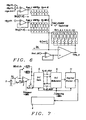
- Fig. 6 illustrates how the coarse and the fine current sources are generated
- the currents I DAC-Coarse and I DAC-Fine are generated by a correspondent constant voltage across correspondent resistors R DAC_F or R DAC_C .
- the resistors are referred to the PTA 3 gain resistors R f1 and R f7 .
- FIG. 7 shows an offset extraction for coarse- and fine loop for I FL compensation branches.
- a further step to the compensation of the current IFL generated by ambient light is a closed loop compensation.
- the ADC is scaled to deliver digital output from 25% to 85% of its analog input from 0% to 100%.
- the input for the digital-to-analog conversion performed by the resistor arrays R DAC_COARSE and R DAC-FINE is set by the digital Calibration and Correction Unit 9.
- the 15 bit output of the fifth order sinc filter 11 is used for this digital-to-analog conversion.
- the offset values OFF C and OFF F have been stored in a previous step during offset extraction in the digital Calibration and Correction Unit 9.
- the current IFL generated by ambient light is subtracted through a close-loop compensation from the signal current.
- the output of the coarse compensation steps is used as the input for the fine compensation.
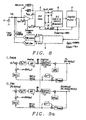
- Fig. 9b illustrates a preferred embodiment of an ambient light compensation sequence.
- the first step of the offset extraction is the coarse offset extraction during 14 ⁇ sec followed by the fine offset extraction during another 14 ⁇ sec.
- the offset extraction is followed by a coarse compensation performed in two steps, each of which has a duration of again 14 ⁇ sec.
- the current IFL generated by ambient light is defined and stored under DACc1[7:0], while no signal from an infrared senser diode is present.
- the value of DACc1 is subtracted from the current I FL and stored under DACc2[7:0].
- a fine compensation follows the coarse compensation also performed in two steps having each also a duration of 14 ⁇ sec. The details of the fine compensation are described in the table below:
- a system calibration is performed.
- the overall system shown in Fig. 1 , performs the digitizing of input current and results in form with gain and offset errors:
- ADout is the output voltage of the circuit
- I IN is the current through the feedback resistors R f 4
- Gsc is the gain of the S-C gain 5
- Vref+ and Vref- are the reference voltages shown in Fig. 1 .
- each raw output of the A/D converter 6 is digitally corrected by substracting the offset and multiplying by the appropriate gain correction term:
- Fig. 10 illustrates how calibration currents ICAL are applied to extract the gain and offset errors during system calibration.
- the LRD 2 is disconnected during the calibration shown in Fig. 10 .
- the table below shows.the parameters of calibration, wherein V CAL is an input voltage and V PTA_O is an output voltage of the PTA 3.
- Fig. 11 summarizes the sequence to measure an infrared current pulse.
- Fig. 11 shows the ambient light FL and an infrared signal pulse NL. Furthermore a previous signal pulse 110 is indicated.
- Step ⁇ 1 and ⁇ 2 system calibration
- Step ⁇ 3 offset extraction for ambient light, i FL , compensation
- Step ⁇ 4 accommotating the ambient light, i FL , compensation
- Step ⁇ 5, ⁇ 6, and ⁇ 7 accommodating the compensated ambient light, I FL0, and infrared pulse, I NL
- ALS Absolute Photometry
- IALS Absolute Photometry
- Fig. 12 shows a sequence to measure an absolute photometry light, I ALS (N R ).
- the single step to measure the absolute visible light comprises:
- Step ⁇ 1 light, i ALS , measurement
- the factors a and b are known from system calibration and are read from a flash memory.
- Fig. 13 depicts a multi-purpose A/D converter to measure a transmitter LED forward voltage for extraction the ⁇ V diode (T), i.e.the temperature dependency of the forward voltage of a transmitter LED.
- An analog multiplexer 130 sets two different voltages causing two different currents I D1 and I D2 to flow through a transmitter diode.
- the embodiment comprises a switched capacitor gain S-C gain 5, a fourth-order sigma-delta modulator 6 and a two-stage decimation filter 11 and 12 having a 14 bit resolution.
- the extraction of the transmitter LEDs ⁇ V diode (T) can be done by software after the measure sequence; which is illustrated in Fig. 14 .
- the measurement comprises three phases. In a first phase an offset cancellation is performed, in a second phase a first voltage forward of the diode is performed using a low current, in the third phase a voltage forward measurement of the diode is performed using a high current. It is obvious that the second and third phase can be interchanged.
- Fig. 15 illustrates a flowchart of a method invented to accommodate an infrared photodiode current generated by a signal light from a LED diode in presence of ambient light to a rain sensing system. It should be noted that the method invented could also be used for other sensor systems using photodiodes.
- a first step 150 describes the provision of a light receiving photo diode receiving a signal light pulse from a light source and a front end system comprising a continuous-time programmable transresistance amplifier converting input current through multi-scaled feedback resistors into a voltage, a digital unit, an analog-to digital converter and a digital-to-analog converter.
- a next step 151 illustrates calibrating said front-end system by digitally correcting each raw output of the analog-to-digital converter while the photo diode is disconnected.
- Step 152 depicts extracting offset for ambient light compensation.
- Step 153 illustrates accommodating the ambient light compensation;
- step 154 discloses accommodating compensated ambient light and signal light pulse and in step 155 the process flow is resumed with step 151 if the system is still ON, otherwise the process flow goes to END.
Landscapes
- Engineering & Computer Science (AREA)
- Computer Networks & Wireless Communication (AREA)
- Physics & Mathematics (AREA)
- General Physics & Mathematics (AREA)
- Radar, Positioning & Navigation (AREA)
- Remote Sensing (AREA)
- Amplifiers (AREA)
Abstract
Description
- This invention relates generally to a front-end circuit of an electro-optical sensing device and relates more specifically to accommodate an infrared pulse of a light receiving diode (LRD), receiving transmitted light from a light source, in presence of ambient current (ambient light in an LRD) for a rain-sensing system. This performs measurements of the attenuation of reflected infrared LED light due to increased scattering of light by rain.
- The usage of infrared senders and receivers is getting more and more popular and is known for numerous different applications and includes a transmitter (such as an infrared light emitting diode (LED)), which transmits light in the infrared range, and an optical receiver (phototransistor or photodiode or photo resistor), which converts the optical infrared signal into a proportional electrical signal.
- Rain sensing systems should fulfill the following properties:
- 1. Providing a 14-bit dynamic range and 250 kHz output rate for accommodating an infrared pulse with an adequate conversion time in the order of 32µsec.
- 2. Providing a resolution of 14-bit leading to an equivalent dynamic range about 160dB of the infrared photocurrents.
- 3. Providing an ambient light compensation having resolution from e.g.15 mA down to 1 µA with an accommodating time of about 50 µsec.
- 4. Providing an infrared current to ambient current ratio maximized by limiting the photocurrent bandwidth and increasing an analog-to-digital converter resolution.
- 5. Improvement in signal-to-noise ratio provided by correlated double sampling of the sequential measurements from the compensated ambient current and an infrared current pulse.
- 6. In summary, a high resolution, wide dynamic range, power efficiency and low cost are required
- Prior art systems do not cover completely these requirements.
- Solutions dealing with photocurrent front-end systems including ADCs are described in the following patents:
- U. S. Patent (
US 7,019,321 to Kokuryo et al ) proposes a rain sensing device that can estimate the size of raindrops or the like without a large amount of hardware resources, and its sensing method, and a wiper controlling apparatus using the same. In a sensing device, light emitted from a light-emitting member is introduced to a transparent plate, reflected by a sensing surface of the transparent plate and then received by a photo-detector, thereby detecting a condition of the sensing surface. - U. S. Patent Publication (
US 2009/0121889 to Lin et al. ) discloses a proximity sensor including a driver, a photo-diode (PD) and an analog-to-digital converter (ADC). The proximity sensor can also include a controller to control the driver. The driver selectively drives a light source, e.g., an infrared (IR) light emitting diode (LED). The PD, which produces a current signal indicative of the intensity of light detected by the PD, is capable of detecting both ambient light and light produced by the light source that is reflected off an object. The ADC receives one or more portion of the current signal produced by the PD. - U. S. Patent (
US 5,929,982 to Anderson ) describes an active avalanche photo-diode (APD) and a gain control circuit for use in an optical receiver including a bias generator for varying the bias on a variable gain APD in response to bias control values generated by a controller. The controller receives the output of the optical receiver and determines the system noise of the receiver for the various bias control values. The system noise is compared to a threshold value for establishing the optimum bias for optimum gain of the APD. The gain control circuit is useable in an optical receiver in an optical time domain reflectometer (OTDR) for increasing the dynamic range of the OTDR. The optical receiver includes an amplifier section for amplifying the output of the APD and an analog-to-digital converter for receiving and converting the amplified output of the amplifier section to digital values representative of an optical input received at the APD. - A principal object of the present invention is to accommodate a current generated by a photo diode receiving a signal light from a LED in presence of ambient light to a front-end sensor system
- A further object of the invention is to accommodate a current generated by a photo diode receiving a signal light from an infrared LED in presence of ambient light to a front-end circuit of a rain-sensing system.
- A further object of the invention is to achieve a front-end circuit having a high dynamic range.
- A further object of the invention is to achieve a readout circuit with a high signal-to-noise ratio
- A further object of the invention is to maximize an infrared to ambient light ratio.
- A further object of the invention is to increase a front end ADC resolution to 14 bits.
- Moreover an object of the invention is to achieve a dynamic range of 160 dB of the infrared photocurrents.
- In accordance with the objects of this invention a method to accommodate a photodiode current generated by a signal light from a light source in presence of ambient light has been achieved. The method invented comprises, firstly, the steps of: (1) providing a light receiving photo diode receiving a signal light pulse from a light source and a front end system comprising a continuous-time programmable transresistance amplifier converting input current through multi-scaled feedback resistors into a voltage, a digital unit, an analog-to digital converter and a digital-to-analog converter, (2) calibrating said front end system by digitally correcting each raw output of the analog-to-digital converter while the photo diode is disconnected, and (3) extracting offset for ambient light compensation. Furthermore the method invented comprises the steps of (4) accommodating the ambient light compensation, (5) accommodating compensated ambient light and signal light pulse, (6) go back to step (2) if system is ON, otherwise go to step (7), and (7) end.
- In accordance with the objects of this invention a system to accommodate a photo diode current receiving a signal light of a sensor application in presence of ambient light having a high dynamic range has been achieved. The system invented comprises, firstly: said photo diode, receiving a signal light and ambient light, generating an output current; and a front-end circuit comprising: a programmable means to convert said output current of the photo diode to a voltage, a programmable means to amplify said voltage converted from the output current, and an analog-to-digital converter to convert said amplified voltage to digital values. Furthermore the front-end circuit comprises a first filtering means to filter the output of the analog-to-digital converter, a second filtering means to filter the output of the first filtering means, a digital unit receiving input from said first filtering means controlling current digital-to-analog converting means and generation of a current calibrating the system, and said current digital-to-analog converting means to successively subtract off a current generated by ambient light at an input of said programmable means to convert said output current of the photo diode to a voltage.
- In the accompanying drawings forming a material part of this description, there is shown:
-
Fig. 1 shows a block diagram of a circuit for accomodating current generated by a LRD receiving infrared light for a rain-sensing system with ambient light compensation. -
Fig. 2 illustrates a block diagram of the programmable transresistance amplifier (PTA) converting current to voltage, used in a preferred embodiment. -
Fig. 3 shows a programmable switched-capacitor gain stage of the circuit invented. -
Fig. 4 illustrates a block diagram of a switched-capacitor sigma-delta analog-to-digital converter stage of the circuit invented. -
Fig. 5 shows a block diagram of a two-stage digital filter of the circuit invented. -
Fig. 6 illustrates how the coarse and the fine current sources are generated. -
Fig. 7 shows an offset extraction for coarse- and fine loop for IFL compensation branches. -
Fig. 8 depicts a closed-loop for compensation of the current generated by ambient light using a digital mapping factor d mapp =1 / (85% - 25%). -
Fig. 9a illustrates coarse and fine control loops for a closed-loop compensation of ambient light. -
Fig. 9b illustrates a preferred embodiment of an ambient light compensation sequence. -
Fig. 10 illustrates how calibration currents ICAL are applied to extract the gain and offset errors during system calibration. -
Fig. 11 summarizes the sequence to measure an infrared current pulse. -
Fig. 12 shows a sequence to measure an absolute photometry light, IALS (NR). -
Fig. 13 depicts a multi-purpose ADC to measure a transmitter LED forward voltage for extraction the ΔVdiode (T). -
Fig. 14 illustrates a sequence to measure the transmitter LEDs ΔVdiode (T) with a current density ratio=8. -
Fig. 15 illustrates a flowchart of a method invented to accommodate an infrared photodiode current generated by a signal light from a LED diode in presence of ambient light to a rain sensing system. - Systems and methods for circuits for a front end circuit to process signals from a photodiode, receiving in a preferred embodiment of the present invention infrared light from a light source as e.g. a light emitting diode (LED) for a rain sensing system It should be noted that the circuit could also be applied to other sensor systems
- A preferred embodiment of the front-
end circuit 1 invented is illustrated inFig.1 . It comprises a light receiving diode (LRD) 2 receiving infrared light from an infrared LED and generating a current INL , which depends upon the light from the infrared LED. Furthermore thephotodiode 2 generates a current IFL , which depends upon an ambient light. A shunt resistor (not shown) prevents the LRD from going into photovoltaic mode during inactive mode. Other wavelengths than infrared light could be applied with the circuit invented as well. - In order to achieve a high dynamic range the circuit comprises 1 a single-ended continuous-time programmable transresistance amplifier (PTA) 3. The
PTA 3 converts the input current into a voltage. Transresistance refers to the ratio between a change of the output voltage and a related change of an input current. Furthermore thePTA 3 applies a fixed voltage, V+=1.5V, to the LRD photo diode. Thefeedback resistance R f 4 of thePTA 3 consists of 7 scales. Other arrangements of feedback resistors are possible as well. - Moreover a chopping frequency fchopper is applied to the
PTA 3, i.e. a frequency modulation of input offset and 1/f noise, and autozeroing, i.e. correlated double sampling of input offset, to remove 1/f noise and system offset errors. - Furthermore the
circuit 1 comprises a switched-capacitor programmable gain-stage 5 that limits the input bandwidth and amplifies the input span to that of the analog-to-digital (A/D)converter 6. The gain (S-C Gain) of the switched-capacitor gain stage 5 consists of 4 ratios. The combined effect of the adjustingresults 14 current ranges by power of ½: 14.4mA; 7.2mA; ...; 3.6µA; 1.8µA. - The
programmable gain amplifier 3 is clocked in the preferred embodiment by a sampling frequency of 4MHz having a first-order low-pass corner frequency that converts the single-ended signal to a fully differential one, limits the photocurrent bandwidth, and amplifies the input span to that of the A/D converter 6 in order to optimize the signal to noise ratio. - The analog-to-digital (A/D)
converter 6 of the preferred embodiment is a 16x oversampled fourth-order sigma-delta modulator (SDM), employs two-stage digital decimation filter, which deliverers full settled output data in 14µsec having 10-bit resolution and in 32µsec having 14-bit resolution. The fully differential range of the A/D converter is, as full-scale equal to +/- [Vref+ - Vref-] = +/-1.65V, 3.3V centered at VDDx½ = 1.65V. The reference voltages are indicated inFig. 1 : Vref+= 2.475 V and Vref-= 0.825 V. - The A/
D 6 converter employs a two-stagedigital decimation filter 10, which delivers full settled output data in 14 µsec having 10 bit resolution and in 32 µsec having 14 bit resolution. Other types of A/D converters and reference voltages could be deployed as well. -
Block 13 performs the digital normalization. The normalization justifies raw data received from the decimation filter according to stored gain (=a) and offset (=b) correction values, which are calculated from biasing on two measurements at 25% and 75% modulation densities, carried out during system calibration. The output y can be described by an equation:
- In the preferred embodiment the RDAC-Coarse resistance 7 consists of 256- tap resistors and the RDAC-Fine resistance 8 consists of 256-tap resistors having sign-bit. This together generates currents, represented by the I DAC-Coarse and +-I DAC-Fine, to compensate the current generated by the ambient light, IFL , from the
receiver photodiode 2 at thetransresistance amplifier 3 inputs. The resistance RCAL is a replica of the feedback resistance Rf. The resistance RCAL generates a current ICAL , for system offset and gain correction. - It should be noted that all components shown in
Fig. 1 , except theLRD 2, are integrated in one chip, hence realizing a low-cost solution. - The following table illustrates input scales and output resolution of the
DAC 6. The following values, as shown inFig. 1 , are used in the table: IIN is an input current of thePTA 3, R F[1,3,5,7,9,11] are feedback resistors of thePTA 3, V PTA_O is the output voltage of thePTA 3, G SC is the gain of the switched-capacitor gain stage 5, having 4 ratios, V SC_O is the output voltage of the switched-capacitor gain stage 5, D SD is the density of the Sigma-Delta Modulator 6 output, and D SDx2 15 signifies the counts of the 14 bit ADC Digital Output AD out [14:0]. -
Current Range PTA Input PTA Gain PTA Single-ended Output to V+=1.5V S-C Gain S-C Gain Fully-differential Output to VCM=1.65V SDM Output = [VSC-O / (2 *Vref+-)] ADC Digital Output ADout [14:0] NR IIN [A] R F[1,3,5,7,9,11] [Ω] V PTA_O [V PP] G SC V SC_O [V PP] D SD [Density] D SD *215 [Counts] 1 14.4m = Rf1 0.99 1.98 0.85 27'852 12m = 68.8 0.825 2 1.65 0.75 24'576 0m 0 0 0.25 8'192 -2.4m -0.165 -0.33 0.15 4'915 2 7.2m = Rf1 0.495 1.98 0.85 27'852 6m = 68.8 0.4125 4 1.65 0.75 24'576 0m 0 0 0.25 8'192 -1.2m -0.0825 -0.33 0.15 4'915 3 3.6m = Rf3 0.99 1.98 0.85 27'852 3m = 275 0.825 2 1.65 0.75 24'576 0m 0 0 0.25 8'192 -0.6m -0.165 -0.33 0.15 4'915 4 1.8m = Rf3 0.495 1.98 0.85 27'852 1.5m = 275 0.4125 4 1.65 0.75 24'576 0m 0 0 0.25 8'192 -0.3m -0.0825 -0.33 0.15 4'915 5 0.9m = Rf5 0.99 1.98 0.85 27'852 0.75m = 1.1K 0.825 2 1.65 0.75 24'576 0m 0 0 0.25 8'192 -0.15m -0.165 -0.33 0.15 4'915 6 450µ = Rf5 0.495 1.98 0.85 27'852 375µ = 1.1K 0.4125 4 1.65 0.75 24'576 0µ 0 0 0.25 8'192 -75µ -0.0825 -0.33 0.15 4'915 7 225µ = Rf7 0.99 1.98 0.85 27'852 187µ = 4.4K 0.825 2 1.65 0.75 24'576 0µ 0 0 0.25 8'192 -37.5µ -0.165 -0.33 0.15 4'915 8 112.5µ = Rf7 0.495 1.98 0.85 27'852 93.5µ = 4.4K 0.4125 4 1.65 0.75 24'576 0µ 0 0 0.25 8'192 -18.8µ -0.0825 -0.33 0.15 4'915 9 56.3µ = Rf9 0.99 1.98 0.85 27'852 46.8µ = 17.6K 0.825 2 1.65 0.75 24'576 0µ 0 0 0.25 8'192 -9.4µ -0.165 -0.33 0.15 4'915 10 28.2µ = Rf9 0.495 1.98 0.85 27'852 23.4µ = 17.6K 0.4125 4 1.65 0.75 24'576 0µ 0 0 0.25 8'192 -4.7µ -0.0825 -0.33 0.15 4'915 11 14.1µ = Rf11 0.99 1.98 0.85 27'852 11.7µ = 70.4K 0.825 2 1.65 0.75 24'576 0 0 0.25 8'192 0µ -0.165 -0.33 0.15 4'915 -2.4µ 12 7.1µ = Rf11 0.495 1.98 0.85 27'852 5.85µ = 70.4K 0.4125 4 1.65 0.75 24'576 0µ 0 0 0.25 8'192 -1.2µ -0.0825 -0.33 0.15 4'915 13 3.6µ = Rf13 0.495 1.98 0.85 27'852 2.93µ = 140.8K 0.4125 4 1.65 0.75 24'576 0µ 0 0 0.25 8'192 -0.6µ -0.0825 -0.33 0.15 4'915 14 1.8µ = Rf13 0.2475 1.98 0.85 27'852 1.47µ = 140.8K 0.2063 8 1.65 0.75 24'576 0µ 0 0 0.25 8'192 -0.3µ -0.0413 -0.33 0.15 4'915 - The parameters behind resolution shown in the table above are following: the number of current ranges, NR = 14; the ratio between adjacent current ranges, R = 2; and the ADout[14:0] results 19'660 counts which is from 25% to 85% of the fullscale dynamic range of A/D converter and gives the effective number of bits, bits = 14.2. Note that the combination results in an output given in counts = RNR - 1 x 2 bits = 2 27.2 , corresponding to 164dB dynamic range for accommodating an infrared photocurrent.
- For each adjacent current ranges, the ADout[14:0] results in an output given in counts = DSD(Iin) ×215:
- Iin = 0 , ADout[14:0] = D SD(Iin= 0) ×215 =0.25×215 = 8'192;
- Iin = Imax, ADout[14:0] = D SD(Iin= Imax) ×215 =0.85×*215 = 27'852.8;
- Since infrared photodiode currents have quantum noise limited characteristics whereby their noise varies in proportion to the square-root of the signal level as


- Because of this, large currents can be digitized with larger quantization stepsizes without appreciably increasing the total noise. The noise is most critical on the highest range where the input level is the smallest.
- Therefore either increasing A/D converter resolution (linear porportional) or limiting the bandwidth (square-root proportional) is the mechanisms to increase the iFL/iNL ratio (ID =iDN +IFL +INL).
-
Fig. 2 illustrates a block diagram of the programmable transresistance amplifier (PTA) 3 converting current to voltage, used in a preferred embodiment. - The output voltage is given by

wherein iIN is the input current of thePTA 3 and Rf is the feedback resistor selected out ofresistors array 4. Thedevice 1/f noise and offset are continuously modulated out by fchopper = 1 MHz and suppressed by the digital filters. - The components, R and C, built a first-order low-pass corner frequency in the preferred embodiment above 125 kHz that acts as anti-aliasing filter to behind switched-
capacitor circuit 5. - The resistors-
array 4 is all built by series or parallel combination of two elementary resistors, Rf3 = 275'Ω and Rf7 = 4.4 K'Ω, as Rf1 = Rf3 /4, Rf3, Rf5 = 4 xRf3, Rf7, Rf9 = 4 xRf7, Rf11 = 16 xRf7 and Rf13 = 32 xRf7. Mismatch between any resistors Rf corresponds to a deviation of the output counts and then limits the accuracy. For this reason calibration current ICAL is added. - The selector-switches used to select a resistor out of the
resistor array 4, which are pMOS and nMOS transistors have the same W/L ratio, are also stepped with weight (2048µm /0.35µm, 512µm /0.35µm, 128µm /0.35µm, 32µm /0.35µm, 8µm /0.35µm, 2µm /0.35µm), decreasing for higher resistance value, for each branch of the array, wide enough to ensure that the temperature dependency is about 2 % of its voltage drop. - The mismatch in consecutive ratios (Rf, N+1/Rf, N and Rf, N /Rf, N-1) causes a discontinuity gain error of (1 +/- err) / (1 -/+ err) ~1 -/+ err. A mismatch of integrated resistors-array done to 2% yields a discontinuity gain error about -/+2%.
- These gain errors can be corrected down to less than 0.01 %, as well as the temperature deviation of the gain, when system calibration is performed during every measurement.
-
Fig. 3 shows a preferred embodiment of the programmable switched-capacitor (S/C)gain stage 5 of the circuit invented. - The
S-C gain stage 5 is a correleted-double-sampling (=2xfs) switched-capacitor instrumentation amplifier with gain ratios, GSC = 1, 2, 4, and 8, provided by capacitors C 2 and C 1. Thedevice 1/f noise and offset are subsequently sampled on capacitors Ccds inclock phase 1 and canceled inclock phase 2. An additional branch comprising capacitors C3 and C2 results the low-pass -3dB corner frequency, fC = 62.5 kHz. - The
numbers Fig. 3 signify are nonoverlapping clocks, which are related to the 4 MHz sampling clock.Number 1 corrsponds to the high phase of the 4 MHz sampling clock;number 2 corresponds to the low phase of the 4 MHz sampling clock. - Thereby, the input bandwidth has been limited, reducing the contribution of white noise. The single-ended input is adapted to the fully differential output between 0.825V and 2.475V by using the sampling sequence in the two paths of the input circuit. The sampling freuqnece is, fS = 4 MHz.
- The transfer function of the S/C gain stage is::

The low-pass corner frequency, fC=62.5 kHz, can be bypassed by disconnecting the capacitor branch of C3 . -
Fig. 4 illustrates a block diagram of a switched-capacitor sigma-delta analog-to-digital (A/D)converter stage 6 of the circuit invented.Fig. 4 shows a preferred embodiment comprising an analog sigma-delta modulator 40 and digitalnoise cancellation logic 41. - Low oversampling ratio of 16 related to a sampling clock, fS = 4 MHz, led to a fourth-order architectural approach to achieve a 14-bit resolution. A two+one+one cascaded switched-capacitor sigma-delta A/D converter is deployed where each delayed integrator has a transfer function z-1 / (1-z-1), is clocked by fS = 4 MHz. This structure is stable since they benefit cascaded low-order modulator loops to enhance their noise shaping proporty.
- Single-
bit quantizers 42 are used with differential quantization levels, (Vref+ - Vref-) =1.65V and (Vref- - Vref+) = -1.65V, centered at VDD*½ =1.65V providing full-scale ranging 3.3V (100% density). - If X is the signal and Qn is the quantization noise, then the output Y of the digital
noise cancelation logic 41 is
Thedigital cancelation logic 41 is an integral part of the sigma-delta A/D converter 40, which results a fourth-order high-pass filter of the quantization noise Qn. - The digital output Y is an oversampled fourth-order noise-shaped signal, the complete A/D converter requires a digital decimation filter to perform down-sampling and out-band noise filtering.
- The digital filter has been selected to provide a 15-bit resolution maintainning the signal-to-quantization noise ratio (SQNR) and fast impulse response. Since a fast settling defines a minimum width of the infrared pulse and accommodating time of an ambient light compensation.
-
Fig. 5 shows a block diagram of a two-stage digital filter of a preferred embodiment the circuit invented. The approach comes in a two-stage digital filter as shown. The inpout Y correponds to the output shown inFig. 4 .. - The first stage comprises a
noise cancelation logic 50 and a modified fifth- order sinc filter 11 with the down-sampling ratio of 8. In signal processing, a sinc filter is an idealized filter that removes all frequency components above a given bandwidth, leaves the low frequencies alone, and has linear phase. The filter's impulse response is a sinc function in the time domain, and its frequency response is a rectangular function. - It is an "ideal" low-pass filter in the frequency sense, perfectly passing low frequencies, perfectly cutting high frequencies; and thus may be considered to be a brick-wall filter.Other low pass filter could be used alternatively. The transfer function of the sinc filter is:

The output rate is 500kHz of thedigital filter 11 and the impulse response is 14 µsec. - The second stage is a 9-tap finit impulse response (FIR)
filter 12 having same input and output rate of 500 kHz. Its transfer function is:
- The impulse response time of the second stage is 18 µsec. The output rate of the
FIR filter 12 is then lowered by 2 to 250kHz. - The combination of fourth-order sigma-delta A/
D converter 6 and first digital filter 11 (sigma-delta ADC 6 and sinc filter 11) results an output rate of 500 kHz and an impulse response, TCONV1 = 14 µsec, having 10-bit resolution. - The complete A/ D converter (fourth-order sigma-
delta ADC 6, sincfilter 11, and FIR filter 12) results an output rate of 250 kHz and an impulse response, TCONV = 32 µsec, having 14-bit resolution. The reduction of an output rate of 500 kHz from theFIR filter 12 to the output rate of 250 kHz is performed in aload dump block 51. - A first step to the compensation of the current IFL generated by ambient light, as shown in
Fig. 1 , is the generation of coarse and fine current sources.Fig. 6 illustrates how the coarse and the fine current sources are generated - The currents I DAC-Coarse and I DAC-Fine are generated by a correspondent constant voltage across correspondent resistors RDAC_F or RDAC_C . The resistors are referred to the
PTA 3 gain resistors Rf1 and Rf7 . As mentioned above in the description of thePTA 6 Rf1 is built by a parallel combination of the elementary resistor Rf3 = 275 'Ω, namely Rf1 = Rf3/4 and Rf7 = 4.4 k'Ω. In this case, all resistors are matched, the dependencies on the supply voltage and on the temperature deviation of the single-ended reference voltage are canceled. - 1. I DAC-COARSE = [VCS/ (Rf1*256)]*(DACC[7:0] +1) and VCS = 0.99V + V+;
I DAG-COARSE (Msb) = 14.4mA and IDAC-COARSE (Lsb) = 56.25 µA. - 2. I DAC-FINE = +-[VFN / (Rf7 *256)]*(DACF[7:0]+1) and VFN = +/-0.99V + V+;
I DAC-FINE (Msb) = 225 µA and IDAC-FINE (Lsb) = 0.88 µA - The current IFL is flowing from the junction with Vpta_o = I FL× Rf + V+; the current IDAC_COARSE +/- IDAC_FINE flows in the junction with Vpta_o = - (IDAC-COARSE +/- IDAC-FINE ) × Rf + V+. The total current flows to the feedback resistor, Rf, and results the output voltage Vpta_o = [IFL -(IDAC_COARSE +/IDAC_FINE )] × Rf + V+.
- Another step to the compensation of the current IFL generated by ambient light, as shown in
Fig. 1 , is a removal of system-offset errors.Fig. 7 shows an offset extraction for coarse- and fine loop for IFL compensation branches. - In order to perform offset extraction the front
infrared diode 2 is disconnected and theADC 6 is set with conversion time, TCONV1 =14 µsec for the offset extraction. The following steps are performed for the offset extraction: - 1. set Rf =
Nr 1, the offset of coarse loop is measured and stored in OFFC in the digital calibration andCorrection Unit 9. - 2. set Rf =
Nr 7, the offset of fine loop is measured and stored in OFFF in the digital calibration andCorrection Unit 9. - A further step to the compensation of the current IFL generated by ambient light is a closed loop compensation.
Fig. 8 depicts a closed-loop for compensation of the current generated by ambient light using a digital mapping factor d mapp =1 / (85% - 25%). The ADC is scaled to deliver digital output from 25% to 85% of its analog input from 0% to 100%. The digital mapping factor dmapp = (100% - 0%) / (85% - 25%), since the DACC[7:0] and DACF[7:0] are scaled from 0% to 100% as h'0=0 and h'FF = IMSB. - The input for the digital-to-analog conversion performed by the resistor arrays RDAC_COARSE and RDAC-FINE is set by the digital Calibration and Correction Unit 9.The 15 bit output of the fifth order sinc filter 11 is used for this digital-to-analog conversion. The input for the conversion to the analog value of IDAC-COARSE is DACc[7:0] = dMAPP x(sinc5[15:0] - OFFc[25%]); the input for the conversion to the analog value of IDAC_fine is DACF[7:0] = ± dMAPP x(sinc5[15:0] - OFFF[25%]). As described above the offset values OFFC and OFFF have been stored in a previous step during offset extraction in the digital Calibration and
Correction Unit 9. -
Fig. 9a illustrates coarse and fine control loops for a closed-loop compensation of the current IFL generated by ambient light, wherein the digital mapping factor is dmapp = 1/(85% - 25%). The current IFL generated by ambient light is subtracted through a close-loop compensation from the signal current. - The output of the coarse compensation steps is used as the input for the fine compensation..
- The table below describes in detail the operation of the circuit of
Fig. 9a , namely the coarse and fine compensation of ambient light.. -
Fig. 9b illustrates a preferred embodiment of an ambient light compensation sequence. Before a compensation of ambient light starts an offset extraction has to be performed..
As described above the first step of the offset extraction is the coarse offset extraction during 14 µsec followed by the fine offset extraction during another 14 µsec. The offset extraction is followed by a coarse compensation performed in two steps, each of which has a duration of again 14 µsec. In the first step of the coarse compensation the current IFL generated by ambient light is defined and stored under DACc1[7:0], while no signal from an infrared senser diode is present. In the second step of the coarse compensation the value of DACc1 is subtracted from the current IFL and stored under DACc2[7:0]. A fine compensation follows the coarse compensation also performed in two steps having each also a duration of 14 µsec. The details of the fine compensation are described in the table below: - The following table illustrates the compensation steps of
Fig. 9b in more detail: -
Step I Φ4_1 set NR = 1, i.e. Rf =Rf1 and GSC =2; measures FL: sinc_out = FL; set DACC1[7:0] = dmappx(sinc_out - OFFC[7:0]); Step II Φ 4_1 measure (FL - DACC1): sinc_out = (FL - DACC1); set DACC2[7:0] = DACC1[7:0] + dmapp *(sinc_out - OFFC[7:0]); -
Step III Φ 4_3 set NR = 7, i.e. Rf =Rf7 and GSC =2; measure (FL - DACC2): sinc_out = (FL - DACC2); if {sinc_out} > OFFF[7:0]; (FL - DACC2 >0); set 'sign-bit' =0; (for analog +VFN generation); set DACF1[7:0] = dmapp *(sinc_out - OFFF[7:0]); else if {sinc_out} < OFFF[7:0]; (FL - DACC2 <0); set `sign-bit' =1; (for analog -VFN generation); set DACF1[7:0]= - dmapp *(sinc_out - OFFF[7:0]); Step IV Φ 4_3 measure (FL - DACC2 - DACF1): sinc_out = (FL - DACC2 - DACF1); Case I {'sign-bif' = 0}: set DACF2[7:0] = DACF1[7:0] + dmapp *(sinc_out - OFFF[7:0]); Case II {'sign-bit' = 1}: set DACF2[7:0]= DACF1[7:0] - dmapp *(sinc_out - OFFF[7:0]). - In order to compensate gain and offset errors a system calibration is performed. The overall system, shown in
Fig. 1 , performs the digitizing of input current and results in form with gain and offset errors:
wherein, as shown inFig. 1 , ADout is the output voltage of the circuit, IIN is the current through thefeedback resistors R f 4, Gsc is the gain of theS-C gain 5, and Vref+ and Vref- are the reference voltages shown inFig. 1 . - To obtain a high degree of linearity, each raw output of the A/
D converter 6 is digitally corrected by substracting the offset and multiplying by the appropriate gain correction term:
- The parameters b[NR] and a[NR] are digitally extracted by adding two equivalent inputs, ICAL's, during system calibration:
- 1. ADRAW(25%, NR) := set Rf(NR), GSC(NR), and ICAL=0;
- 2. ADRAW(75%, NR) := set Rf(NR), GSC(NR), and ICAL=[VCAL /RfNR)].
- 3. b[NR] = 213 - ADRAW(25%, NR); a[NR] = 214 / [ADCraw(75%, NR) - ADCraw(25%, NR)].
-
Fig. 10 illustrates how calibration currents ICAL are applied to extract the gain and offset errors during system calibration. TheLRD 2 is disconnected during the calibration shown inFig. 10 . The table below shows.the parameters of calibration, wherein VCAL is an input voltage and VPTA_O is an output voltage of thePTA 3.Current Range PTA input PTA gain PTA out, s.e at V+=1.5 V SC gain SC out, f.d at VCM=1.65 V SDM Output ADRAW [14:0] NR VCAL[V] RF[□] VPTA_O[VPP] GSC VSC_O[VPP] D SD[Density] DSD *215 [Isb] ICAL(25%) = 0; ICAL(75%) = -VCAL /RF 1 0; 0.825 68.8 0; 0.825 2 0; 1.65 0.25; 0.75 213; 2 0; 0.4125 0; 0.4125 4 (213+214) 3 0; 0.825 275 0; 0.825 2 0; 1.65 0.25; 0.75 213; 4 0; 0.4125 0; 0.4125 4 (213+214 5 0; 0.825 1.1K 0; 0.825 2 0; 1.65 0.25; 0.75 213; 6 0; 0.4125 0; 0.4125 4 (213+214) 7 0; 0.825 4.4K 0; 0.825 2 0; 1.65 0.25; 0.75 213; 8 0; 0.4125 0; 0.4125 4 (213+214) 9 0; 0.825 17.6K 0; 0.825 2 0; 1.65 0.25; 0.75 213; 10 0; 0.4125 0; 0.4125 4 (213+214) 11 0; 0.825 70.4K 0; 0.825 2 0; 1.65 0.25; 0.75 213; 12 0; 0.4125 0; 0.4125 4 (213+214) 13 0; 0.4125 140.8K 0; 0.4125 4 0; 1.65 0.25; 0.75 213; 14 0; 0.2063 0; 0.2063 8 (213+214) - In regard of infrared pulse measurement, using the circuitry outlined above an infrared signal pulse from the
LRD 2 is measured in 7 steps for one current range as illustrated inFig. 11. Fig. 11 summarizes the sequence to measure an infrared current pulse.Fig. 11 shows the ambient light FL and an infrared signal pulse NL. Furthermore a previous signal pulse 110 is indicated. - The steps of the sequence of
Fig. 11 comprise: - Front Infrared LRD is disconnected; two measurements are executed with an A/D conversion time, TCONV =32 µsec.
- The switched-capacitor low-pass filter sector, fC=62.5KHz, and the second-stage digital filter are bypassed; two measurements are executed with an A/D conversion time, TCONV1=14 µsec.
- Front Infrared LRD is connected; four subsequent measurements are executed with an A/D conversion time, TCONV1 =14 µsec.
- The switched-capacitor low-pass filter sector, fC=62.5KHz, and the second-stage digital filter are enabled; three measurements are executed with an ADC conversion time, TCONV =32 µsec.
- The results are performed by digitally subtract of the measurements Φ 6 and Φ 5 (=INL), and of the measurements,
Φ 7 and Φ 5 (= Δ IFL), which are characterized as correlated double sampling (CDS) with a CDS frequence, FCDS =1 / TCONV. - It has to be noted that the CDS achieves a first-order high-pass factor, (1-z-1), which increases the in-band (=fCDS) contribution of uncorrelated white noise power by 3 dB due to the twice sampling; however it attenuates the in-band correlated noise power and all components with frequency below the fCDS /2. Therefore improves the total SNR (signal to noise ratio) for given pulse width of TCONV.
- Another embodiment of the invention can be used for Absolute Photometry (ALS) measurement. The measurement of the absolute visible light, IALS, is executed in 1 step for one current range.
Fig. 12 shows a sequence to measure an absolute photometry light, IALS (NR). The single step to measure the absolute visible light comprises: - Front Infrared photodiode is connected; current range is selected; read gain correction factor in memory; one measurement is executed with an A/D conversion time, TCONV = 32 µsec. The factors a and b are known from system calibration and are read from a flash memory.
-
Fig. 13 depicts a multi-purpose A/D converter to measure a transmitter LED forward voltage for extraction the ΔVdiode (T), i.e.the temperature dependency of the forward voltage of a transmitter LED. This can be performed by a third embodiment of the present invention. Ananalog multiplexer 130 sets two different voltages causing two different currents ID1 and ID2 to flow through a transmitter diode. Furthermore the embodiment comprises a switched capacitorgain S-C gain 5, a fourth-order sigma-delta modulator 6 and a two-stage decimation filter Fig. 14 . -
Fig. 14 illustrates a sequence to measure the transmitter LEDs ΔV diode (T) with a current density ratio=8 using the third embodiment of the invention shown inFig. 13 .The measurement comprises three phases. In a first phase an offset cancellation is performed, in a second phase a first voltage forward of the diode is performed using a low current, in the third phase a voltage forward measurement of the diode is performed using a high current. It is obvious that the second and third phase can be interchanged. -
Fig. 15 illustrates a flowchart of a method invented to accommodate an infrared photodiode current generated by a signal light from a LED diode in presence of ambient light to a rain sensing system. It should be noted that the method invented could also be used for other sensor systems using photodiodes. Afirst step 150 describes the provision of a light receiving photo diode receiving a signal light pulse from a light source and a front end system comprising a continuous-time programmable transresistance amplifier converting input current through multi-scaled feedback resistors into a voltage, a digital unit, an analog-to digital converter and a digital-to-analog converter. Anext step 151 illustrates calibrating said front-end system by digitally correcting each raw output of the analog-to-digital converter while the photo diode is disconnected. Step 152 depicts extracting offset for ambient light compensation. Step 153 illustrates accommodating the ambient light compensation;step 154 discloses accommodating compensated ambient light and signal light pulse and instep 155 the process flow is resumed withstep 151 if the system is still ON, otherwise the process flow goes to END. - While the invention has been particularly shown and described with reference to the preferred embodiments thereof, it will be understood by those skilled in the art that various changes in form and details may be made without departing from the spirit and scope of the invention.
Claims (32)
- A method to accommodate a photodiode current generated by a signal light from a light source in presence of ambient light, comprising the following steps:(1) providing a light receiving photo diode receiving a signal light pulse from a light source and a front end system comprising a continuous-time programmable transresistance amplifier converting input current through multi-scaled feedback resistors into a voltage, a digital unit, an analog-to digital converter and a digital-to-analog converter;(2) calibrating said front-end system by digitally correcting each raw output of the analog-to-digital converter while the photo diode is disconnected;(3) extracting offset for ambient light compensation;(4) accommodating the ambient light compensation;(5) accommodating compensated ambient light and signal light pulse;(6) go back to step (2) if system is ON, otherwise go to step (7); and(7) end.
- The method of claim 1 wherein said calibration is performed by subtracting an offset and multiplying by an appropriate correction term, e.g. by means of two measurements.
- The method of claim 2 wherein parameters for said calibration are digitally extracted by adding two equivalent calibration currents to an input of the transresistance amplifier.
- The method of claim 1 wherein said offset extraction is performed for each a coarse loop and a fine loop of compensation branches for ambient light
- The method of claim 4 wherein said offset extraction for the coarse loop and for the fine loop is performed by activating different resistors of said multi-scaled feedback resistors.
- The method of claim 1 wherein said ambient light compensation is performed by closed-loop compensation.
- The method of claim 1 wherein said accommodation of ambient light compensation comprises a fine offset extraction, a first coarse ambient light compensation, a second coarse ambient light compensation, a first fine ambient light compensation, and a second fine ambient light compensation wherein the results of said offset extraction are used as input for the ambient light compensation and the results of the coarse ambient light compensation are used as input for the fine ambient light compensation..
- The method of claim 7 wherein each of said accommodation steps is characterized by using a specific resistor out of said multi-scaled feedback resistors.
- The method of claim 7 wherein the accommodation of compensated ambient light and the signal light pulse is performed by digitally subtract of measurements of the signal light pulse and of measurements of the ambient light, which are characterized as correlated double sampling.
- The method of claim 1 wherein said signal light is an infrared light.
- The method of claim 1 wherein said analog-to-digital converter is a sigma-delta analog-to digital converter.
- The method of claim 11 wherein a digital cancelation logic is an integral part of the sigma-delta A/D converter, which results a fourth-order high-pass filter of the quantization noise Qn.
- The method of claim 11 wherein large currents are digitized with larger quantization step sizes than smaller currents.
- The method of claim 1 wherein a coarse and a fine current digital-to-analog converter in parallel are used to generate a current as an input of the transresistance amplifier compensation the ambient light.
- The method of claim 1 wherein a calibration current source is used to correct offset of the system and gain errors.
- The method of claim 1 wherein said digital unit is controlling the accommodation of the current generated by ambient light, selecting a range of the current generated by the signal light, and the calibration of the front end system.
- The method of claim 1 wherein said method is used for a rain-sensing system.
- A system to accommodate a photo diode current receiving a signal light of a sensor application in presence of ambient light having a high dynamic range comprises:said photo diode, receiving a signal light and ambient light, generating an output current; anda front-end circuit comprising:a programmable means to convert said output current of the photo diode to a voltage;a programmable means to amplify said voltage converted from the output current;an analog-to-digital converter to convert said amplified voltage to digital values;a first filtering means to filter the output of the analog-to-digital converter;a second filtering means to filter the output of the first filtering means;a digital unit receiving input from said first filtering means controlling current digital-to-analog converting means and generation of a current calibrating the system; andsaid current digital-to-analog converting means to successively subtract off a current generated by ambient light at an input of said programmable means to convert said output current of the photo diode to a voltage.
- The system of claim 18 wherein said photo diode is receiving an infrared light signal.
- The system of claim 18 wherein said sensor application is a rain-sensing system.
- The system of claim 18 wherein said programmable means to convert current to voltage is an operational amplifier based on a operational amplifier which is a programmable single ended continuous-time programmable transresistance amplifier, said operational amplifier having a number of parallel feedback resistors to achieve a high dynamic range, wherein active feedback resistors can be selected by said digital control unit.
- The system of claim 18 wherein said programmable means to amplify said voltage converted from the output current is a switched-capacitor programmable gain amplifier clocked by sampling frequency having a first-order low-pass corner frequency that converts a single-ended signal to fully differential.
- The system of claim 18 wherein said analog-to-digital converter is a switched-capacitor fourth-order oversampled sigma-delta A/D converter, e.g. a 16x oversampled switched-capacitor fourth-order sigma-delta A/D converter.
- The system of claim 18 wherein said sigma-delta A/D converter comprises a single-bit quantizer with differential quantization levels, or said sigma-delta A/D converter employs a two-stage digital decimation filter that is clocked by sampling frequency of 4MHz and provides 14-bit conversion resolution with TCONV = 32µ sec.
- The system of claim 24 wherein a first stage of the decimation filter is fifth- order SINC filter.
- The system of claim 25 wherein a second stage of the decimation filters is a finite impulse response filter, e.g. a 9-tap finite impulse response filter having a rate of 500kHz.
- The system of claim 18 wherein a digital normalization block is connected to the output of said second filtering means, and justifies raw data received from the decimation filter according to a stored gain and offset correction values, which are calculated from biasing on two measurements at different modulation densities, carried out during system calibration.
- The system of claim 18 wherein said current digital-to-analog converting means are a coarse 8-bit DAC and a fine 7-bit current DAC generating each a current IDAC_COARSE and correspondently IDAC_FINE to successively subtract off a current generated by ambient light at the input of the programmable means to convert said output current of the photo diode to a voltage before receiving a current generated by the signal light, said currents IDAC_COARSE and correspondently IDAC_FINE are generated by a constant voltage across resistors which are referred to feedback resistors of said programmable means to convert said output current of the photo diode.
- The system of claim 18 wherein a chopping frequency is applied to the programmable means to convert said output current of the photo diode to a voltage and autozeroing to remove 1/f noise and system offset errors.
- The system of claim 18 wherein the system is used as a multi-purpose circuit for other measurements wherein said digital unit and said current digital-to analog converting means can be omitted and a multiplexer at the input can be added, e.g. for the measurement of a feed-forward voltage of a photo diode as function of temperature.
- The system of claim 18 wherein a shunt resistor prevents said photo diode from going into photovoltaic mode during inactive mode.
- The system of claim 18 wherein a resistor and a capacitor in series in a feedback loop of the programmable means to convert said output current of the photo diode to a voltage are deployed to build a first-order low-pass corner frequency.
Priority Applications (1)
| Application Number | Priority Date | Filing Date | Title |
|---|---|---|---|
| EP10368019.5A EP2322395B1 (en) | 2009-11-17 | 2010-03-23 | Infrared photocurrent front-end ADC for rain-sensing system with ambient light compensation |
Applications Claiming Priority (2)
| Application Number | Priority Date | Filing Date | Title |
|---|---|---|---|
| EP09368043 | 2009-11-17 | ||
| EP10368019.5A EP2322395B1 (en) | 2009-11-17 | 2010-03-23 | Infrared photocurrent front-end ADC for rain-sensing system with ambient light compensation |
Publications (2)
| Publication Number | Publication Date |
|---|---|
| EP2322395A1 true EP2322395A1 (en) | 2011-05-18 |
| EP2322395B1 EP2322395B1 (en) | 2016-03-02 |
Family
ID=43598462
Family Applications (1)
| Application Number | Title | Priority Date | Filing Date |
|---|---|---|---|
| EP10368019.5A Active EP2322395B1 (en) | 2009-11-17 | 2010-03-23 | Infrared photocurrent front-end ADC for rain-sensing system with ambient light compensation |
Country Status (2)
| Country | Link |
|---|---|
| US (1) | US8097853B2 (en) |
| EP (1) | EP2322395B1 (en) |
Cited By (2)
| Publication number | Priority date | Publication date | Assignee | Title |
|---|---|---|---|---|
| JP2016516461A (en) * | 2013-03-16 | 2016-06-09 | エンパティカ エスアールエル | Device for measuring electrodermal activity with current compensation |
| CN112968702A (en) * | 2021-01-21 | 2021-06-15 | 许继集团有限公司 | Processing system and method for improving sampling precision of ADC (analog to digital converter) small signal in processor |
Families Citing this family (23)
| Publication number | Priority date | Publication date | Assignee | Title |
|---|---|---|---|---|
| US8692200B2 (en) * | 2010-01-06 | 2014-04-08 | Avago Technologies General Ip (Singapore) Pte. Ltd. | Optical proximity sensor with improved dynamic range and sensitivity |
| US8786481B1 (en) * | 2011-11-07 | 2014-07-22 | Zerowatt Technologies, Inc. | Method and apparatus for event detection and adaptive system power reduction using analog compression engine |
| WO2013150716A1 (en) * | 2012-04-03 | 2013-10-10 | パナソニック株式会社 | Visible light reception device and visible light reception method |
| CN102735343A (en) * | 2012-07-04 | 2012-10-17 | 昆明物理研究所 | Method for improving charge storage capacity of readout circuit by applying charge deduction technology |
| US9130070B2 (en) * | 2013-04-25 | 2015-09-08 | Analog Devices, Inc. | Four-stage circuit architecture for detecting pulsed signals |
| US10056868B2 (en) | 2013-04-25 | 2018-08-21 | Analog Devices, Inc. | Four-stage circuit architecture for detecting pulsed signals |
| US9733275B2 (en) | 2014-07-25 | 2017-08-15 | Analog Devices, Inc. | Circuit architecture for mode switch |
| EP2996250B1 (en) | 2014-09-11 | 2020-02-19 | ams AG | Optical sensor arrangement and method for generating an analog output signal |
| US10069414B2 (en) | 2015-04-01 | 2018-09-04 | Infineon Technologies Austria Ag | Switching voltage regulator input voltage and current sensing |
| TWI575229B (en) * | 2016-01-08 | 2017-03-21 | 聯笙電子股份有限公司 | Signal Processing Method and Sensor Thereof |
| US10389242B2 (en) | 2017-02-01 | 2019-08-20 | Infineon Technologies Austria Ag | Voltage and current sensing calibration for switching voltage regulators |
| CN107422876B (en) * | 2017-07-18 | 2019-06-28 | Oppo广东移动通信有限公司 | A kind of control method of proximity sensor, device, storage medium and mobile terminal |
| US10224812B1 (en) * | 2017-10-13 | 2019-03-05 | Infineon Technologies Austria Ag | Sensing network mismatch compensation for switching voltage regulator with input voltage and current sensing |
| CN110797364B (en) * | 2019-11-08 | 2022-01-11 | 京东方科技集团股份有限公司 | Detection substrate, detection panel and photoelectric detection device |
| DE102020211101A1 (en) * | 2020-09-03 | 2022-03-03 | Robert Bosch Gesellschaft mit beschränkter Haftung | Optical environment sensor and vehicle |
| KR20220086783A (en) | 2020-12-16 | 2022-06-24 | 삼성전자주식회사 | Electronic device and operating method of electronic device |
| DE102021100438B3 (en) | 2021-01-12 | 2022-05-12 | Elmos Semiconductor Se | Device for simultaneous delta-sigma analog-to-digital conversion of multiple input signals |
| US11867557B2 (en) * | 2021-07-30 | 2024-01-09 | Analog Devices International Unlimited Company | Automatic ambient light cancellation method for optical front-end methods and apparatus |
| US12015427B2 (en) | 2022-04-05 | 2024-06-18 | Stmicroelectronics (Research & Development) Limited | Photodiode current compatible input stage for a sigma-delta analog-to-digital converter |
| CN115102550B (en) * | 2022-08-29 | 2022-12-09 | 苏州联讯仪器有限公司 | Multi-bandwidth optical port sampling circuit for oscilloscope |
| CN118670512B (en) * | 2023-03-16 | 2026-05-05 | 深圳市速腾聚创科技有限公司 | Circuits, methods, and radar for detecting ambient light |
| CN116698091B (en) * | 2023-06-12 | 2026-02-24 | 传周半导体科技(上海)有限公司 | Circuit for reducing ambient light noise in encoder |
| CN119200017B (en) * | 2024-10-14 | 2025-06-06 | 上海天易合芯微电子有限公司 | Self-adaptive ambient light elimination proximity light detection sensor |
Citations (5)
| Publication number | Priority date | Publication date | Assignee | Title |
|---|---|---|---|---|
| US5929982A (en) | 1997-02-04 | 1999-07-27 | Tektronix, Inc. | Active APD gain control for an optical receiver |
| WO2000041023A1 (en) * | 1998-12-31 | 2000-07-13 | Libbey-Owens-Ford Co. | Moisture sensor with digital signal processing filtering |
| US20040056199A1 (en) * | 2002-09-25 | 2004-03-25 | O'connor Christopher J. | Infrared obstacle detection in the presence of sunlight |
| US7019321B2 (en) | 2001-01-10 | 2006-03-28 | Niles Co., Ltd. | Sensing device and its sensing method, and wiper controlling apparatus using the same |
| US20090121889A1 (en) | 2007-11-14 | 2009-05-14 | Intersil Americas Inc. | Proximity sensors and methods for sensing proximity |
Family Cites Families (6)
| Publication number | Priority date | Publication date | Assignee | Title |
|---|---|---|---|---|
| DE19729103A1 (en) | 1997-07-08 | 1999-01-14 | Bosch Gmbh Robert | Device and method for operating a rain sensor |
| DE19740364A1 (en) | 1997-09-13 | 1999-03-25 | Bosch Gmbh Robert | Device for operating an optoelectronic rain sensor |
| DE10214421B4 (en) | 2002-03-30 | 2007-08-09 | Hella Kgaa Hueck & Co. | Method for operating a rain sensor, in particular for motor vehicles |
| DE102007034606A1 (en) | 2007-07-25 | 2009-01-29 | Robert Bosch Gmbh | System for detecting optical signals with a rain sensor and method |
| DE102007048858A1 (en) | 2007-10-11 | 2009-04-16 | Robert Bosch Gmbh | Method for operating a rain sensor, in particular for motor vehicles |
| US7868294B2 (en) * | 2007-11-15 | 2011-01-11 | Silicon Laboratories Inc. | Apparatus and method for display control using ambient light measurement signal from an infrared receiver |
-
2009
- 2009-11-20 US US12/592,259 patent/US8097853B2/en active Active
-
2010
- 2010-03-23 EP EP10368019.5A patent/EP2322395B1/en active Active
Patent Citations (5)
| Publication number | Priority date | Publication date | Assignee | Title |
|---|---|---|---|---|
| US5929982A (en) | 1997-02-04 | 1999-07-27 | Tektronix, Inc. | Active APD gain control for an optical receiver |
| WO2000041023A1 (en) * | 1998-12-31 | 2000-07-13 | Libbey-Owens-Ford Co. | Moisture sensor with digital signal processing filtering |
| US7019321B2 (en) | 2001-01-10 | 2006-03-28 | Niles Co., Ltd. | Sensing device and its sensing method, and wiper controlling apparatus using the same |
| US20040056199A1 (en) * | 2002-09-25 | 2004-03-25 | O'connor Christopher J. | Infrared obstacle detection in the presence of sunlight |
| US20090121889A1 (en) | 2007-11-14 | 2009-05-14 | Intersil Americas Inc. | Proximity sensors and methods for sensing proximity |
Non-Patent Citations (1)
| Title |
|---|
| SUNE DUUN ET AL: "High quantum efficiency annular backside silicon photodiodes for reflectance pulse oximetry in wearable wireless body sensors; High quantum efficiency annular backside silicon photodiodes", JOURNAL OF MICROMECHANICS & MICROENGINEERING, INSTITUTE OF PHYSICS PUBLISHING, BRISTOL, GB, vol. 20, no. 7, 1 July 2010 (2010-07-01), pages 75020, XP020175502, ISSN: 0960-1317 * |
Cited By (4)
| Publication number | Priority date | Publication date | Assignee | Title |
|---|---|---|---|---|
| JP2016516461A (en) * | 2013-03-16 | 2016-06-09 | エンパティカ エスアールエル | Device for measuring electrodermal activity with current compensation |
| US10506944B2 (en) | 2013-03-16 | 2019-12-17 | Empatica Srl | Apparatus for electrodermal activity measurement with current compensation |
| US11766187B2 (en) | 2013-03-16 | 2023-09-26 | Empatica Srl | Apparatus for electrodermal activity measurement with current compensation |
| CN112968702A (en) * | 2021-01-21 | 2021-06-15 | 许继集团有限公司 | Processing system and method for improving sampling precision of ADC (analog to digital converter) small signal in processor |
Also Published As
| Publication number | Publication date |
|---|---|
| US8097853B2 (en) | 2012-01-17 |
| EP2322395B1 (en) | 2016-03-02 |
| US20110114842A1 (en) | 2011-05-19 |
Similar Documents
| Publication | Publication Date | Title |
|---|---|---|
| EP2322395B1 (en) | Infrared photocurrent front-end ADC for rain-sensing system with ambient light compensation | |
| US8665130B2 (en) | ADC, a temperature sensor, a non-contact transponder, and a method of converting analog signals to digital signals | |
| US8787776B2 (en) | Optical receiver with monolithically integrated photodetector | |
| JP5154659B2 (en) | Multi-bit sigma-delta modulator with reduced number of bits in the feedback path | |
| Wu et al. | 9.1 A current-sensing front-end realized by a continuous-time incremental ADC with 12b SAR quantizer and reset-then-open resistive DAC achieving 140dB DR and 8ppm INL at 4kS/s | |
| US11876539B2 (en) | Current to digital converter circuit, optical front end circuit, computed tomography apparatus and method | |
| US20100283650A1 (en) | multi-bit sigma-delta modulator with reduced number of bits in feedback path | |
| EP1418674A1 (en) | Converter, circuit and method for compensation of non-idealities in continuous time sigma delta converters | |
| Mitteregger et al. | A 14b 20mW 640MHz CMOS CT/spl Delta//spl Sigma/ADC with 20MHz Signal Bandwidth and 12b ENOB | |
| US9419643B2 (en) | Delta sigma modulator | |
| Caldwell et al. | A Reconfigurable $\Delta\Sigma $ ADC With Up to 100 MHz Bandwidth Using Flash Reference Shuffling | |
| CN108900195B (en) | Oversampling analog-to-digital converter and dynamic error calibration method of feedback digital-to-analog converter | |
| Ying et al. | A sub-pA current sensing front-end for transient induced molecular spectroscopy | |
| EP3843277A1 (en) | Analogue-to-digital conversion device comprising two cascading stages of analogue-to-digital conversion with successive approximation register and noise shaping, and associated electronic sensor | |
| JP2004525580A (en) | Analog-digital modulator | |
| KR20230125271A (en) | Adaptive charge measurement circuit for data converter | |
| US7098834B2 (en) | Multi-mode analog to digital converter | |
| KR101875464B1 (en) | Current readout circuit having a improved power consumption and dynamic-range | |
| Yu et al. | 82 dB SNDR 20-channel incremental ADC with optimal decimation filter and digital correction | |
| Dorrer et al. | A 2.2 mW, continuous-time sigma-delta ADC for voice coding with 95dB dynamic range in a 65nm CMOS process | |
| Qureshi et al. | An incremental-ΔΣ ADC with 106-dB DR for reconfigurable class-D audio amplifiers | |
| Naus et al. | Multibit oversampled Sigma Delta A/D converters as front end for CD players | |
| Lee et al. | A 14 b 23 MS/s 48 mW Resetting $\Sigma\Delta $ ADC | |
| Krenzke et al. | A 140 dB equivalent dynamic range receiver interface for an infrared rain-sensing IC | |
| Baumer et al. | Design and evaluation of a CMOS-photosensor with in-pixel sigma-delta modulator for X-ray computed tomography |
Legal Events
| Date | Code | Title | Description |
|---|---|---|---|
| PUAI | Public reference made under article 153(3) epc to a published international application that has entered the european phase |
Free format text: ORIGINAL CODE: 0009012 |
|
| AK | Designated contracting states |
Kind code of ref document: A1 Designated state(s): AT BE BG CH CY CZ DE DK EE ES FI FR GB GR HR HU IE IS IT LI LT LU LV MC MK MT NL NO PL PT RO SE SI SK SM TR |
|
| AX | Request for extension of the european patent |
Extension state: AL BA ME RS |
|
| 17P | Request for examination filed |
Effective date: 20111118 |
|
| 17Q | First examination report despatched |
Effective date: 20130917 |
|
| RIC1 | Information provided on ipc code assigned before grant |
Ipc: G01S 7/486 20060101ALI20150413BHEP Ipc: B60S 1/08 20060101AFI20150413BHEP |
|
| GRAP | Despatch of communication of intention to grant a patent |
Free format text: ORIGINAL CODE: EPIDOSNIGR1 |
|
| INTG | Intention to grant announced |
Effective date: 20150616 |
|
| RIN1 | Information on inventor provided before grant (corrected) |
Inventor name: TYRRELL, JULIAN Inventor name: CANG, JI |
|
| GRAS | Grant fee paid |
Free format text: ORIGINAL CODE: EPIDOSNIGR3 |
|
| GRAA | (expected) grant |
Free format text: ORIGINAL CODE: 0009210 |
|
| AK | Designated contracting states |
Kind code of ref document: B1 Designated state(s): AT BE BG CH CY CZ DE DK EE ES FI FR GB GR HR HU IE IS IT LI LT LU LV MC MK MT NL NO PL PT RO SE SI SK SM TR |
|
| REG | Reference to a national code |
Ref country code: GB Ref legal event code: FG4D |
|
| REG | Reference to a national code |
Ref country code: AT Ref legal event code: REF Ref document number: 777779 Country of ref document: AT Kind code of ref document: T Effective date: 20160315 Ref country code: CH Ref legal event code: EP |
|
| REG | Reference to a national code |
Ref country code: IE Ref legal event code: FG4D |
|
| REG | Reference to a national code |
Ref country code: DE Ref legal event code: R096 Ref document number: 602010030863 Country of ref document: DE |
|
| PGFP | Annual fee paid to national office [announced via postgrant information from national office to epo] |
Ref country code: GB Payment date: 20160315 Year of fee payment: 7 |
|
| REG | Reference to a national code |
Ref country code: NL Ref legal event code: MP Effective date: 20160302 |
|
| REG | Reference to a national code |
Ref country code: LT Ref legal event code: MG4D |
|
| REG | Reference to a national code |
Ref country code: AT Ref legal event code: MK05 Ref document number: 777779 Country of ref document: AT Kind code of ref document: T Effective date: 20160302 |
|
| PG25 | Lapsed in a contracting state [announced via postgrant information from national office to epo] |
Ref country code: FI Free format text: LAPSE BECAUSE OF FAILURE TO SUBMIT A TRANSLATION OF THE DESCRIPTION OR TO PAY THE FEE WITHIN THE PRESCRIBED TIME-LIMIT Effective date: 20160302 Ref country code: HR Free format text: LAPSE BECAUSE OF FAILURE TO SUBMIT A TRANSLATION OF THE DESCRIPTION OR TO PAY THE FEE WITHIN THE PRESCRIBED TIME-LIMIT Effective date: 20160302 Ref country code: GR Free format text: LAPSE BECAUSE OF FAILURE TO SUBMIT A TRANSLATION OF THE DESCRIPTION OR TO PAY THE FEE WITHIN THE PRESCRIBED TIME-LIMIT Effective date: 20160603 Ref country code: ES Free format text: LAPSE BECAUSE OF FAILURE TO SUBMIT A TRANSLATION OF THE DESCRIPTION OR TO PAY THE FEE WITHIN THE PRESCRIBED TIME-LIMIT Effective date: 20160302 Ref country code: NO Free format text: LAPSE BECAUSE OF FAILURE TO SUBMIT A TRANSLATION OF THE DESCRIPTION OR TO PAY THE FEE WITHIN THE PRESCRIBED TIME-LIMIT Effective date: 20160602 |
|
| PG25 | Lapsed in a contracting state [announced via postgrant information from national office to epo] |
Ref country code: BE Free format text: LAPSE BECAUSE OF NON-PAYMENT OF DUE FEES Effective date: 20160331 Ref country code: LT Free format text: LAPSE BECAUSE OF FAILURE TO SUBMIT A TRANSLATION OF THE DESCRIPTION OR TO PAY THE FEE WITHIN THE PRESCRIBED TIME-LIMIT Effective date: 20160302 Ref country code: PL Free format text: LAPSE BECAUSE OF FAILURE TO SUBMIT A TRANSLATION OF THE DESCRIPTION OR TO PAY THE FEE WITHIN THE PRESCRIBED TIME-LIMIT Effective date: 20160302 Ref country code: AT Free format text: LAPSE BECAUSE OF FAILURE TO SUBMIT A TRANSLATION OF THE DESCRIPTION OR TO PAY THE FEE WITHIN THE PRESCRIBED TIME-LIMIT Effective date: 20160302 Ref country code: NL Free format text: LAPSE BECAUSE OF FAILURE TO SUBMIT A TRANSLATION OF THE DESCRIPTION OR TO PAY THE FEE WITHIN THE PRESCRIBED TIME-LIMIT Effective date: 20160302 Ref country code: SE Free format text: LAPSE BECAUSE OF FAILURE TO SUBMIT A TRANSLATION OF THE DESCRIPTION OR TO PAY THE FEE WITHIN THE PRESCRIBED TIME-LIMIT Effective date: 20160302 Ref country code: LV Free format text: LAPSE BECAUSE OF FAILURE TO SUBMIT A TRANSLATION OF THE DESCRIPTION OR TO PAY THE FEE WITHIN THE PRESCRIBED TIME-LIMIT Effective date: 20160302 |
|
| PG25 | Lapsed in a contracting state [announced via postgrant information from national office to epo] |
Ref country code: EE Free format text: LAPSE BECAUSE OF FAILURE TO SUBMIT A TRANSLATION OF THE DESCRIPTION OR TO PAY THE FEE WITHIN THE PRESCRIBED TIME-LIMIT Effective date: 20160302 Ref country code: IS Free format text: LAPSE BECAUSE OF FAILURE TO SUBMIT A TRANSLATION OF THE DESCRIPTION OR TO PAY THE FEE WITHIN THE PRESCRIBED TIME-LIMIT Effective date: 20160702 |
|
| REG | Reference to a national code |
Ref country code: CH Ref legal event code: PL |
|
| PG25 | Lapsed in a contracting state [announced via postgrant information from national office to epo] |
Ref country code: SK Free format text: LAPSE BECAUSE OF FAILURE TO SUBMIT A TRANSLATION OF THE DESCRIPTION OR TO PAY THE FEE WITHIN THE PRESCRIBED TIME-LIMIT Effective date: 20160302 Ref country code: SM Free format text: LAPSE BECAUSE OF FAILURE TO SUBMIT A TRANSLATION OF THE DESCRIPTION OR TO PAY THE FEE WITHIN THE PRESCRIBED TIME-LIMIT Effective date: 20160302 Ref country code: RO Free format text: LAPSE BECAUSE OF FAILURE TO SUBMIT A TRANSLATION OF THE DESCRIPTION OR TO PAY THE FEE WITHIN THE PRESCRIBED TIME-LIMIT Effective date: 20160302 Ref country code: CZ Free format text: LAPSE BECAUSE OF FAILURE TO SUBMIT A TRANSLATION OF THE DESCRIPTION OR TO PAY THE FEE WITHIN THE PRESCRIBED TIME-LIMIT Effective date: 20160302 Ref country code: PT Free format text: LAPSE BECAUSE OF FAILURE TO SUBMIT A TRANSLATION OF THE DESCRIPTION OR TO PAY THE FEE WITHIN THE PRESCRIBED TIME-LIMIT Effective date: 20160704 |
|
| REG | Reference to a national code |
Ref country code: DE Ref legal event code: R097 Ref document number: 602010030863 Country of ref document: DE |
|
| REG | Reference to a national code |
Ref country code: IE Ref legal event code: MM4A |
|
| PG25 | Lapsed in a contracting state [announced via postgrant information from national office to epo] |
Ref country code: IT Free format text: LAPSE BECAUSE OF FAILURE TO SUBMIT A TRANSLATION OF THE DESCRIPTION OR TO PAY THE FEE WITHIN THE PRESCRIBED TIME-LIMIT Effective date: 20160302 Ref country code: BE Free format text: LAPSE BECAUSE OF FAILURE TO SUBMIT A TRANSLATION OF THE DESCRIPTION OR TO PAY THE FEE WITHIN THE PRESCRIBED TIME-LIMIT Effective date: 20160302 |
|
| PLBE | No opposition filed within time limit |
Free format text: ORIGINAL CODE: 0009261 |
|
| STAA | Information on the status of an ep patent application or granted ep patent |
Free format text: STATUS: NO OPPOSITION FILED WITHIN TIME LIMIT |
|
| PG25 | Lapsed in a contracting state [announced via postgrant information from national office to epo] |
Ref country code: DK Free format text: LAPSE BECAUSE OF FAILURE TO SUBMIT A TRANSLATION OF THE DESCRIPTION OR TO PAY THE FEE WITHIN THE PRESCRIBED TIME-LIMIT Effective date: 20160302 Ref country code: LI Free format text: LAPSE BECAUSE OF NON-PAYMENT OF DUE FEES Effective date: 20160331 Ref country code: IE Free format text: LAPSE BECAUSE OF NON-PAYMENT OF DUE FEES Effective date: 20160323 Ref country code: CH Free format text: LAPSE BECAUSE OF NON-PAYMENT OF DUE FEES Effective date: 20160331 |
|
| 26N | No opposition filed |
Effective date: 20161205 |
|
| REG | Reference to a national code |
Ref country code: FR Ref legal event code: ST Effective date: 20170109 |
|
| PG25 | Lapsed in a contracting state [announced via postgrant information from national office to epo] |
Ref country code: BG Free format text: LAPSE BECAUSE OF FAILURE TO SUBMIT A TRANSLATION OF THE DESCRIPTION OR TO PAY THE FEE WITHIN THE PRESCRIBED TIME-LIMIT Effective date: 20160602 Ref country code: SI Free format text: LAPSE BECAUSE OF FAILURE TO SUBMIT A TRANSLATION OF THE DESCRIPTION OR TO PAY THE FEE WITHIN THE PRESCRIBED TIME-LIMIT Effective date: 20160302 |
|
| PG25 | Lapsed in a contracting state [announced via postgrant information from national office to epo] |
Ref country code: FR Free format text: LAPSE BECAUSE OF NON-PAYMENT OF DUE FEES Effective date: 20160502 |
|
| PG25 | Lapsed in a contracting state [announced via postgrant information from national office to epo] |
Ref country code: MT Free format text: LAPSE BECAUSE OF FAILURE TO SUBMIT A TRANSLATION OF THE DESCRIPTION OR TO PAY THE FEE WITHIN THE PRESCRIBED TIME-LIMIT Effective date: 20160302 |
|
| GBPC | Gb: european patent ceased through non-payment of renewal fee |
Effective date: 20170323 |
|
| PG25 | Lapsed in a contracting state [announced via postgrant information from national office to epo] |
Ref country code: GB Free format text: LAPSE BECAUSE OF NON-PAYMENT OF DUE FEES Effective date: 20170323 |
|
| PG25 | Lapsed in a contracting state [announced via postgrant information from national office to epo] |
Ref country code: HU Free format text: LAPSE BECAUSE OF FAILURE TO SUBMIT A TRANSLATION OF THE DESCRIPTION OR TO PAY THE FEE WITHIN THE PRESCRIBED TIME-LIMIT; INVALID AB INITIO Effective date: 20100323 Ref country code: CY Free format text: LAPSE BECAUSE OF FAILURE TO SUBMIT A TRANSLATION OF THE DESCRIPTION OR TO PAY THE FEE WITHIN THE PRESCRIBED TIME-LIMIT Effective date: 20160302 |
|
| PG25 | Lapsed in a contracting state [announced via postgrant information from national office to epo] |
Ref country code: MK Free format text: LAPSE BECAUSE OF FAILURE TO SUBMIT A TRANSLATION OF THE DESCRIPTION OR TO PAY THE FEE WITHIN THE PRESCRIBED TIME-LIMIT Effective date: 20160302 Ref country code: TR Free format text: LAPSE BECAUSE OF FAILURE TO SUBMIT A TRANSLATION OF THE DESCRIPTION OR TO PAY THE FEE WITHIN THE PRESCRIBED TIME-LIMIT Effective date: 20160302 Ref country code: MT Free format text: LAPSE BECAUSE OF FAILURE TO SUBMIT A TRANSLATION OF THE DESCRIPTION OR TO PAY THE FEE WITHIN THE PRESCRIBED TIME-LIMIT Effective date: 20160331 Ref country code: LU Free format text: LAPSE BECAUSE OF NON-PAYMENT OF DUE FEES Effective date: 20160323 Ref country code: MC Free format text: LAPSE BECAUSE OF FAILURE TO SUBMIT A TRANSLATION OF THE DESCRIPTION OR TO PAY THE FEE WITHIN THE PRESCRIBED TIME-LIMIT Effective date: 20160302 |
|
| REG | Reference to a national code |
Ref country code: DE Ref legal event code: R082 Ref document number: 602010030863 Country of ref document: DE |
|
| PGFP | Annual fee paid to national office [announced via postgrant information from national office to epo] |
Ref country code: DE Payment date: 20260304 Year of fee payment: 17 |