WO2013150716A1 - Visible light reception device and visible light reception method - Google Patents
Visible light reception device and visible light reception method Download PDFInfo
- Publication number
- WO2013150716A1 WO2013150716A1 PCT/JP2013/001397 JP2013001397W WO2013150716A1 WO 2013150716 A1 WO2013150716 A1 WO 2013150716A1 JP 2013001397 W JP2013001397 W JP 2013001397W WO 2013150716 A1 WO2013150716 A1 WO 2013150716A1
- Authority
- WO
- WIPO (PCT)
- Prior art keywords
- point
- visible light
- unit
- falling
- rising
- Prior art date
Links
Images


Classifications
-
- H—ELECTRICITY
- H04—ELECTRIC COMMUNICATION TECHNIQUE
- H04B—TRANSMISSION
- H04B10/00—Transmission systems employing electromagnetic waves other than radio-waves, e.g. infrared, visible or ultraviolet light, or employing corpuscular radiation, e.g. quantum communication
- H04B10/60—Receivers
- H04B10/61—Coherent receivers
- H04B10/63—Homodyne, i.e. coherent receivers where the local oscillator is locked in frequency and phase to the carrier signal
-
- H—ELECTRICITY
- H04—ELECTRIC COMMUNICATION TECHNIQUE
- H04B—TRANSMISSION
- H04B10/00—Transmission systems employing electromagnetic waves other than radio-waves, e.g. infrared, visible or ultraviolet light, or employing corpuscular radiation, e.g. quantum communication
- H04B10/11—Arrangements specific to free-space transmission, i.e. transmission through air or vacuum
- H04B10/114—Indoor or close-range type systems
- H04B10/116—Visible light communication
-
- H—ELECTRICITY
- H04—ELECTRIC COMMUNICATION TECHNIQUE
- H04B—TRANSMISSION
- H04B10/00—Transmission systems employing electromagnetic waves other than radio-waves, e.g. infrared, visible or ultraviolet light, or employing corpuscular radiation, e.g. quantum communication
- H04B10/60—Receivers
- H04B10/66—Non-coherent receivers, e.g. using direct detection
- H04B10/69—Electrical arrangements in the receiver
- H04B10/693—Arrangements for optimizing the preamplifier in the receiver
Definitions
- the present invention relates to a visible light receiving apparatus and a visible light receiving method for detecting identification ID information based on a change in visible light illumination.
- GPS Global Positioning System
- the GPS measures the position of the mobile terminal by receiving radio waves from a plurality of satellites. For this reason, it is difficult to use GPS in underground malls and buildings where radio waves from satellites are blocked.
- Patent Document 1 describes a visible light communication system that can be used as a lighting fixture.
- FIG. 9 shows a configuration of a visible light communication system according to Patent Document 1.
- the communication system 100 using visible light includes a transmission device 110 and a reception device 130.
- the communication system 100 modulates the visible light output from the light emitting element 117 of the transmission device 110 according to a QAM (Quadrature Amplitude Modulation) signal using a high-frequency carrier wave, and then modulates the visible light by the light receiving element 133 of the reception device 130.
- the received QAM modulated signal is demodulated.
- the QAM modulated signal is a QAM modulated visible light signal.
- the communication system 100 has a function of keeping the level of a received signal constant by using an AGC (Automatic Gain 36 Control) 136.
- the AGC 136 reduces the gain (Gain) when a strong level signal is input to prevent signal saturation, and increases the gain (Gain) to increase the signal when a weak level signal is input. It has a function to keep the level of
- the communication system according to Patent Document 2 includes a modulation unit that modulates a subcarrier, a blinking control unit that blinks visible light based on the modulation signal, and a ratio control that emits visible light by changing a ratio of light emission time.
- stable data communication can be performed by using a modulation signal using a high-frequency carrier wave.
- Patent Document 1 uses a QAM modulated signal in which a frequency is multiplexed using a carrier wave
- Patent Document 2 uses a modulated signal using a sub-carrier to blink visible light, thereby stabilizing stable data. Communication is possible.
- the portable terminal (receiving device) receives visible light including identification ID information from a lighting device (transmitting device) installed in the underground shopping area, the position of the portable terminal is measured even in the underground shopping area. Is possible.
- the communication distance between the lighting device and the mobile terminal changes depending on the position of the user of the mobile terminal, and changes every moment when the user walks.
- the level of the received signal rapidly attenuates.
- the level of the received signal when the communication distance is 4 m is attenuated to about 1/64 compared to the level of the received signal when the communication distance is 0.5 m.
- the level of the output signal is automatically adjusted to be constant by the AGC 136, and then the visible light signal is demodulated using the output signal of the AGC circuit. ing.
- the AGC circuit configuration is complicated. For example, it is very difficult to realize an AGC that operates stably for a received signal whose signal level changes from 1 to 1/64.
- the AGC configuration is simplified, but the circuit configuration of the transmitter and the receiver is complicated.
- a delay may occur in the circuit response, which may cause distortion in the output signal of AGC.
- the communication path visible light path
- the conventional visible light receiving apparatus has a problem that the circuit configuration is complicated and the response may be slow.
- the present invention is for solving the above-described conventional problems, can cope with a large change in the level of a visible light signal without using AGC, and receives and demodulates a visible light signal in a short time.
- An object of the present invention is to provide a visible light receiving apparatus and a visible light receiving method.
- the visible light receiving device of the present invention receives visible light that changes in intensity according to a modulation signal that is position-modulated at each symbol time, and outputs a voltage signal corresponding to the amount of received light of the visible light.
- a first converter that outputs, an amplifying unit that cuts a DC component included in the voltage signal and amplifies and outputs the AC component; and processes the voltage signal output from the amplifying unit to produce the modulated signal
- a processing unit that outputs a corresponding demodulated signal, and the processing unit includes a second conversion unit that AD converts the voltage signal output from the amplification unit into an AD conversion value for each sampling time;
- a first calculation unit that calculates a difference digital value by a difference calculation using the AD conversion value, and a + side reference value and a ⁇ side reference value corresponding to a plurality of peak values of the difference digital values.
- a second arithmetic unit and the difference data A detection unit for detecting a rising point at which a tall value is larger than the + side reference value and a falling point at which the differential digital value is smaller than the ⁇ side reference value; and the rising point and the rising point A first sample period between the falling point detected immediately after the point and a second sample period between the falling point and the rising point detected immediately after the falling point; A third calculation unit for calculating, and a fourth calculation unit for calculating the demodulated signal for each symbol time based on the first sample period and the second sample period alternately generated in time series It is characterized by that.
- the visible light receiving method of the present invention is a visible light receiving method for acquiring information included in visible light, and the visible light receiving method corresponds to the received visible light.
- a first step of AD converting a voltage signal into an AD conversion value at each sampling time by a first conversion unit; a second step of calculating a difference digital value by a difference calculation using the plurality of AD conversion values;
- a visible light receiving apparatus and a visible light receiving apparatus that can cope with a large change in the level of a visible light signal and can receive and demodulate a visible light signal in a short time without using AGC.
- a method can be provided.
- FIG. 1 is a configuration diagram of a visible light communication system including a receiving apparatus according to the first embodiment.
- FIG. 2A is a configuration diagram of the microcomputer according to the first embodiment.
- FIG. 2B is a flowchart illustrating processing steps of the microcomputer according to the first embodiment.
- FIG. 3 is a waveform diagram for explaining the operation of the receiving apparatus according to the first embodiment, where (a) shows the illumination light Lm and the disturbance light Dt, and (b) shows the voltage signal Jm.
- C) is a figure which shows the amplified signal Km
- (d) is a figure which shows the rising point Rm and the falling point Fm.
- FIG. 1 is a configuration diagram of a visible light communication system including a receiving apparatus according to the first embodiment.
- FIG. 2A is a configuration diagram of the microcomputer according to the first embodiment.
- FIG. 2B is a flowchart illustrating processing steps of the microcomputer according to the first embodiment.
- FIG. 3 is a waveform diagram for explaining
- FIG. 4 is a waveform diagram for explaining the operation of the receiving apparatus according to the modification of the first embodiment, where (a) is a diagram showing the illumination light Lm and the disturbance light Dt, and (b) is a voltage diagram. It is a figure which shows the signal Jm, (c) is a figure which shows the amplified signal Km, (d) is a figure which shows the rising point Rm and the falling point Fm.
- FIG. 5 is a configuration diagram of a visible light communication system including the receiving device according to the second embodiment.
- FIG. 6 is a flowchart of processing steps of the microcomputer unit according to the second embodiment.
- FIG. 7 is a waveform diagram for explaining the operation of the receiving apparatus according to the second embodiment, where (a) shows the illumination light Lm and disturbance light Dt, and (b) shows the voltage signal Jm. (C) is a figure which shows the amplified signal Km, (d) is a figure which shows the rising point Rm and the falling point Fm.
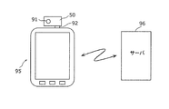
- FIG. 8 is a configuration diagram of a position information providing system including a mobile terminal to which a receiving apparatus according to the third embodiment is connected.
- FIG. 9 is a configuration diagram of a conventional communication system.
- FIG. 1 is a configuration diagram of a visible light communication system including the receiving device 10 according to the first embodiment.
- the receiving device 10 is an example of a visible light receiving device.
- FIG. 2A is a configuration diagram of the microcomputer 13 according to the first embodiment.
- the microcomputer 13 is an example of a processing unit.
- FIG. 2B is a flowchart showing processing steps of the microcomputer 13.
- FIGS. 3A to 3D are waveform diagrams for explaining the operation of the receiving apparatus 10.
- the visible light communication system includes a receiving device 10 and a lighting device 20.
- the illumination device 20 is an example of a visible light illumination device (visible light transmission device).
- the receiving device 10 includes a first conversion unit 11, an amplification unit 12, and a microcomputer 13.
- the first converter 11 is an example of an optical voltage converter that converts light into a voltage (electric signal).
- the amplifying unit 12 is an example of a DC cut amplifying unit that amplifies an AC component by cutting a DC component of the voltage signal.
- the first converter 11 has a light receiving element (not shown).
- the light receiving element converts the received illumination light into an electrical signal.
- the illumination light in the first embodiment is visible light emitted from the illumination device 20.
- the illumination light is light that does not use a subcarrier, and is light that is strong and weak in response to a modulation signal that is position-modulated every predetermined symbol time.
- the first converter 11 outputs a voltage signal Jm corresponding to the intensity of the received illumination light to the amplifier 12.
- the width of the unit pulse constituting the modulation signal is defined as a slot time, and a period corresponding to 4 slot times is defined as one symbol time.
- the DC component of the voltage signal Jm output from the first converter 11 is cut by the amplifying unit 12, so that the DC component corresponding to the disturbance light having a constant intensity among the voltage signals included in the voltage signal Jm. Cut. In this way, the noise component can be removed from the voltage signal by cutting the DC component using the amplifying unit 12.
- the amplifying unit 12 cuts the DC component of the voltage signal Jm and amplifies the AC component of the voltage signal Jm with a predetermined gain. As described above, by amplifying the AC component of the voltage signal Jm using the amplifying unit 12, the voltage signal corresponding to the identification ID information can be detected more easily.
- the AC component of the amplified voltage signal Jm is output to the microcomputer 13 as the output signal Km.
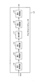
- the microcomputer 13 includes a second conversion unit 14, a first calculation unit 15, a second calculation unit 16, a detection unit 17, a third calculation unit 18, and a fourth calculation unit 19.
- the second conversion unit 14 is an example of an AD conversion unit.
- the first calculation unit 15 is an example of a difference calculation unit
- the second calculation unit 16 is an example of a reference calculation unit
- the detection unit 17 is an example of a point detection unit
- the third calculation unit 18 is an interval calculation.
- the fourth calculation unit 19 is an example of a demodulation calculation unit.
- the second conversion unit 14 which is an example of an AD conversion unit, AD-converts the output signal Km output from the amplification unit 12 into an AD conversion value for each predetermined sampling time Ts, and converts the converted AD conversion value to the first value.
- the result is output to the calculation unit 15.
- the output signal Km is an analog signal
- the AD conversion value is a digital signal.
- the first calculation unit 15 calculates the difference between the plurality of AD conversion values using the plurality of AD conversion values at each of the plurality of sampling points. Then, the first calculation unit 15 outputs the difference digital value obtained by the calculation of the difference to the second calculation unit 16.
- the second calculation unit 16 extracts a difference digital value that is continuous for four symbol times or more, and calculates a peak value (or an absolute peak value) of the extracted difference digital value. Then, a + side reference value corresponding to the + side peak value (or + side absolute peak value) and a ⁇ side reference value corresponding to the ⁇ side peak value (or ⁇ side absolute peak value) are obtained. To the detection unit 17.
- the peak value means the extreme value (partially protruding value) of the extracted difference digital value
- the absolute peak value means the absolute value of the extracted difference digital value.
- the positive reference value in the first embodiment is, for example, a value obtained by adding a predetermined value and approximately 1/3 of the maximum value of the peak value (or absolute peak value).
- the negative side reference value is, for example, a value obtained by multiplying the positive side reference value by -1.
- the predetermined value is a positive value including 0, and may be 0.
- the detecting unit 17 detects a rising point and a falling point that occur alternately in time series from the rising point and the falling point in time series as the selected rising point and the selected falling point.
- the time point when the difference digital value becomes larger than the + side reference value in the time series is set as the rising point, and the time point when the difference digital value becomes smaller than the ⁇ reference value in the time series falls. The point is. Then, the detected selected rising point and selected falling point are output to the third calculation unit 18.
- the third calculation unit 18 detects the first sample period as the number of level 1 samples.
- the first sample period is the number of samples of the difference digital value (first sample period) between the selected rising point and the selected falling point immediately after.
- the third calculator 18 detects the second sample period as the number of level 0 samples.
- the second sample period is the number of samples of the difference digital value (second sample period) between the selected falling point and the selected rising point immediately after. Then, the detected number of level 1 samples or level 0 samples is output to the fourth arithmetic unit 19.
- the fourth arithmetic unit 19 generates a demodulated code (demodulated signal) for each symbol time based on the first sample period and the second sample period that occur alternately in time series, that is, the number of level 1 samples and the number of level 0 samples. calculate. Thereby, a demodulated signal corresponding to the output signal Km output from the amplifying unit 12 is output from the microcomputer 13. Based on this demodulated signal, the receiving apparatus 10 detects the position of the receiving apparatus 10.
- a demodulated code demodulated signal
- the illumination device 20 that is a visible light transmission device includes a drive unit 21 and an illumination unit 22.
- the driving unit 21 is an example of a position modulation driving unit, and generates a modulation signal having identification ID information.
- the drive unit 21 according to the first embodiment for example, does not use a subcarrier, and creates a modulation signal in which the identification ID information is position-modulated by a 4PPM (Pulse Position Modulation) method for each symbol time.
- 4PPM Pulse Position Modulation
- the illumination unit 22 changes the intensity of the illumination light according to the modulation signal of the drive unit 21.
- the illuminating unit 22 includes a white LED (Light-Emitting) Diode), and increases or decreases the amount of white visible light emission corresponding to the modulation signal.
- the cycle of the intensity of emitted light is, for example, about 1 kHz.
- the illumination part 22 may be comprised by colored visible light LED, such as red LED and blue LED.
- a disturbance light source 25 that generates pulsed disturbance light such as a fluorescent lamp or a display is often present near the illumination device 20.
- the receiving device 10 receives both the illumination light from the illumination device 20 at the place where it is used and the disturbance light from the disturbance light source 25 nearby.
- the first conversion unit 11 of the receiving device 10 When receiving illumination light and disturbance light, the first conversion unit 11 of the receiving device 10 outputs a voltage signal Jm.
- the voltage signal Jm changes according to the amount of received light of visible light such as received illumination light or disturbance light.
- the amplifying unit 12 to which the voltage signal Jm is input outputs the amplified signal Km.
- the amplified signal Km is a signal obtained by amplifying the AC component of the voltage signal Jm of the first converter 11 with a predetermined gain (Gain).
- the microcomputer 13 includes a first step S01 that is an AD conversion step, a second step S02 that is a difference calculation step, a third step S03 that is a reference calculation step, and a point detection step.
- An ID detection step (a twelfth step described later) including a fourth step S04, a fifth step S05 which is an interval calculation step, and a sixth step S06 which is a demodulation calculation step is executed.
- the microcomputer 13 performs the first step S01 to the sixth step S06, thereby AD-converting the amplified signal of the amplifying unit 12 and performing a signal demodulating operation.
- the receiving device 10 can accurately demodulate the identification ID information of the lighting device 20 even when the communication distance between the receiving device 10 and the lighting device 20 changes.
- the reason why the identification ID information can be demodulated with high accuracy is that, in the first embodiment, the voltage signal Jm of the first converter 11 which is a received signal corresponding to a change in the communication distance between the receiving device 10 and the lighting device 20. This is because the configuration has a small influence on the demodulation of the identification ID information even if the ID changes. Therefore, the receiving apparatus 10 according to the first embodiment is configured to be able to cope with a large change in the amount of received light without using AGC (Automatic Gain ⁇ Control) that is necessary for the conventional visible light receiving device. ing.
- AGC Automatic Gain ⁇ Control
- the receiving apparatus 10 has a configuration that can cope with the pulsed disturbance light of the disturbance light source 25 since the operation of the processing step of the microcomputer 13 is devised.
- the illumination light Lm from the illumination device 20 is indicated by a solid line
- the pulsed disturbance light Dt is indicated by a broken line.
- the voltage signal Jm due to the illumination light Lm is indicated by a solid line
- the voltage signal Jmd due to the disturbance light Dt is indicated by a broken line.
- the amplified signal Km based on the illumination light Lm is indicated by a solid line
- the amplified signal Kmd based on the disturbance light Dt is indicated by a broken line.
- FIG. 3D shows a rising point Rm and a falling point Fm. 3A to 3D, the horizontal axis indicates time, and the vertical axis indicates the intensity of each signal.
- identification ID information having a predetermined code length is represented by a modulation signal in which a plurality of symbol times are temporally connected. Therefore, the illumination device 20 in visible light communication emits light by changing the intensity of visible light corresponding to the modulation signal.
- the drive unit 21 of the illumination device 20 shown in FIG. 1 generates a 4PPM modulation signal for each symbol time By and supplies the modulation signal to the illumination unit 22.
- One symbol time By is composed of four slot times (slot times C1, C2, C3, C4).
- the modulated signal of 4PPM is a signal obtained by modulating the time position of one pulse time slot within one symbol time By.
- the fourth slot time (slot time C4) is position-modulated.
- the second slot time By2 from the left the second slot time (slot time C2) is position-modulated.
- the third symbol time By3 from the left the first slot time (slot time C1) is position-modulated.
- the fourth symbol time By4 from the left the third slot time (slot time C3) is position-modulated.
- the illuminating unit 22 of the illuminating device 20 shown in FIG. 1 emits visible illumination light whose intensity changes corresponding to the modulation signal.
- the illumination device 20 emits illumination light in any one of the four slot times C1, C2, C3, and C4 that are continuous every symbol time By based on the identification ID information. Illumination light that is weaker than the illumination light is output.
- the illumination light having a weak slot time C1 is output.
- the identification ID information is code “01”
- illumination light with a weak slot time C2 is emitted.
- the identification ID information is code “10”
- illumination light with a weak slot time C3 is output.
- the identification ID information is code “11”
- the illumination light having a weak slot time C4 is output.
- a high-frequency subcarrier is not used as the modulation signal.
- the illumination light of the illumination device 20 includes an intensity change portion La (a portion where the signal intensity changes in accordance with the modulation signal) and a constant portion Lb (a portion where the signal intensity is constant). It is a synthesized light. That is, as indicated by a solid line in FIG. 3A, the illumination light Lm of the illumination device 20 that is received (received) by the reception device 10 is a combination of the strength change portion La and the constant portion Lb. Since the disturbance light source 25 generates pulsed disturbance light, the disturbance light Dt from the disturbance light source 25 received by the receiving device 10 is pulsed as shown by a broken line in FIG. is there.
- the first converter 11 of the receiving device 10 outputs a voltage signal Jm corresponding to the amount of light received by a light receiving element (not shown).
- FIG. 3B shows the voltage signal Jm output from the first converter 11. Since the light receiving element of the first conversion unit 11 receives the illumination light Lm of the illumination device 20 and the disturbance light Dt of the disturbance light source 25 in a superimposed manner, a voltage signal Jm corresponding to the combined light quantity of both is obtained. Therefore, the voltage signal Jm shown in (b) of FIG. 3 is a signal obtained by synthesizing the influence of the illumination light Lm and the influence of the disturbance light Dt (Jmd portion shown in (b) of FIG. 3).
- the amplifying unit 12 of the receiving device 10 cuts (deletes) the direct current component of the voltage signal Jm from the voltage signal Jm input from the first conversion unit 11, and converts the alternating current component to a predetermined fixed gain (fixed Gain). Amplify. Then, the amplification unit 12 outputs the amplified amplified signal Km.
- FIG. 3 (c) shows the amplified signal Km.
- the amplified signal Km shown in (c) of FIG. 3 has a signal waveform obtained by inverting and amplifying the AC component of the voltage signal Jm with a predetermined fixed gain. For this reason, the amplified signal Km is a signal obtained by synthesizing the influence of the illumination light Lm and the influence of the disturbance light Dt (the Kmd portion shown in FIG. 3C).
- the amplified signal Km output from the amplifying unit 12 is input to the microcomputer 13.
- the structure of the amplification part 12 can also employ
- the amplified signal Km input to the microcomputer 13 is processed in the microcomputer 13 of the receiving apparatus 10 as follows.
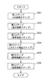
- the microcomputer 13 repeatedly executes the processing steps shown in the flowchart of FIG. 2B at regular time intervals or every trigger by the user. That is, the microcomputer 13 includes a first step (AD conversion step) S01, a second step (difference calculation step) S02, a third step (reference calculation step) S03, and a fourth step (point detection step) S04. And a fifth step (interval calculation step) S05 and a sixth step (demodulation calculation step) S06, and these steps are executed sequentially or partially in parallel.
- the first step S01 is an example of an AD conversion step.
- the first step S01 is a step in which the second conversion unit 14 performs AD conversion on the amplified signal Km output from the amplification unit 12 every predetermined sampling time Ts to obtain an AD conversion value.
- the second step S02 is an example of a difference calculation step.
- the second step S02 is a step in which the first calculation unit 15 performs a difference calculation using AD conversion values at a plurality of sampling points and calculates a difference digital value.
- the third step S03 is an example of a reference calculation step.
- the second arithmetic unit 16 extracts consecutive difference digital values of 4 symbol times or more, and then the + side reference value corresponding to the peak value (or absolute peak value) of the extracted difference digital value This is a step of calculating a negative side reference value.
- the fourth step S04 is an example of a point detection step.
- the fourth step S04 is a step in which the detection unit 17 detects a selected rising point and a selected falling point that occur alternately in time series from the time-series rising point and falling point.
- the fifth step S05 is an example of an interval calculation step.
- the fifth step S05 is a step in which the third arithmetic unit 18 detects the level 1 sample number and the level 0 sample number.
- the sixth step S06 is an example of a demodulation calculation step.
- the sixth step S06 is a step in which the fourth calculation unit 19 calculates a demodulation code for each symbol time based on the number of level 1 samples and the number of level 0 samples alternately generated in time series.
- the second conversion unit 14 performs AD conversion on the input amplified signal Km, which is an analog signal, every predetermined sampling time Ts, and acquires a digitized AD conversion value for a predetermined time length.
- the sampling time Ts is selected to be sufficiently smaller than the symbol time By.
- the predetermined time length is set to be sufficiently long, and is a time length that sufficiently includes the identification ID information of the lighting device 20.
- the 2nd conversion part 14 memorize
- the first calculation unit 15 performs a difference calculation using AD conversion values at a plurality of sampling points, calculates a difference digital value at each sampling point, and stores the time-series difference digital values in the memory.
- the difference between the AD conversion value at the sampling time and the AD conversion value at the two previous sampling time is calculated, and the calculation result is stored in the memory as the difference digital value at that time.
- the digital time value is calculated for each sampling time point by sequentially moving the sampling time point, and the time-series differential digital value is acquired.
- the first calculation unit 15 stores a time-series difference digital value in a memory as necessary.
- the sampling time point is sequentially moved, the difference digital value is calculated for each sampling time point, and the time-series difference digital value is acquired.
- the third step S03 the second arithmetic unit 16 extracts the consecutive difference digital values having four or more symbol times, and the + side reference value corresponding to the peak value (or absolute peak value) of the extracted difference digital value -Get the side reference value.
- the predetermined value may be set to a large positive value so that the identification ID information cannot be demodulated when the time-series difference digital value becomes smaller than the predetermined value.
- the second calculation unit 16 may obtain a + side reference value and a ⁇ side reference value corresponding to the average value of the peak values (or absolute peak values) of the extracted difference digital values.
- the illumination light Lm becomes small (or large)
- the reference value corresponding to the magnitude of the modulation signal included in the illumination light Lm can be easily obtained.
- the detection operation of the rising point and the falling point in the fourth step S04 can be stabilized. That is, by the operation in the third step S03, the fourth step S04 can be stably operated even if the average value of the illumination light Lm changes 100 times.
- the detection unit 17 detects the rising point and the falling point.
- the rising point is a point in time when the time-series difference digital value becomes larger than the + side reference value
- the falling point is a point in time when the time-series difference digital value becomes smaller than the ⁇ side reference value.
- Fig. 3 (d) shows the rising point Rm and the falling point Fm.
- the falling point Fn + 1 and the rising point Rn + 1 are generated by the disturbance light Dt of the disturbance light source 25.
- the detection unit 17 selects a selected rising point and a selected falling point that occur alternately in time series from the time-series rising point and falling point. For example, even when rising points occur continuously or when falling points occur continuously, the selected rising points and selected falling points appear to occur alternately in time series. Elected.
- the detection unit 17 selects the second falling point and the subsequent rising point as the selected falling point and the selected rising point. Don't pick points. That is, the detection unit 17 excludes the second falling point and the subsequent rising point from detection targets.
- the detection unit 17 selects the second rising point and the subsequent falling points as the selected rising point and the selected falling point. Not selected as points. That is, the detection unit 17 excludes the second rising point and the subsequent falling point from the detection target.
- the falling point Fn + 1 and the rising point Rn + 1 caused by the disturbance light can be removed.
- the rising point means the first sampling time point at which the time-series difference digital value becomes larger than the positive reference value.
- the falling point means the first sampling time point at which the time-series differential digital value becomes smaller than the negative reference value.
- the third calculation unit 18 detects the number of level 1 samples and detects the number of level 0 samples.
- the number of samples of the difference digital value between the selected start point immediately after the selected start point is set as the number of level 1 samples, and between the selected start point and the immediately subsequent select start point.
- the number of samples of the difference digital value is the number of level 0 samples.
- the fourth arithmetic unit 19 obtains a demodulation code for each symbol time based on the number of level 1 samples and the number of level 0 samples alternately generated in time series.
- the fourth computing unit 19 detects the identification ID information based on the demodulation code over a plurality of symbol times. Thereby, it can be understood which receiving device 10 has acquired the identification ID information of which lighting device 20. Therefore, the position of the receiving device 10 can be detected.
- the fourth calculation unit 19 may detect the start block code added to the identification ID information in the sixth step S06 and find the first symbol time for starting the code demodulation of the identification ID information.
- the receiving apparatus 10 stably detects the identification ID information of the lighting apparatus 20 that is a visible light transmitting apparatus with a simple configuration that does not use a complicated circuit such as AGC (Automatic Gain Control). can do.
- the receiving device 10 can be modularized and incorporated in a small and lightweight portable terminal (for example, a smartphone) and integrated, or can be attached to a portable terminal such as a smartphone.
- the reception device 10 by performing a series of operations from the first step S01 to the sixth step S06 by the microcomputer 13, the reception device 10 receives the identification ID information of the illumination device 20 with high accuracy and demodulates it. can do. That is, the receiving apparatus 10 according to the first embodiment can perform a normal demodulation operation even if the level of the received visible light signal changes significantly.
- the receiving apparatus 10 when the level of the received signal changes 100 times, the distance changes about 10 times when converted to the communication distance. Since the receiving apparatus 10 according to the first embodiment uses this characteristic, it is used in applications where the communication distance of visible light communication changes significantly, such as a portable terminal that receives visible light illumination of the lighting apparatus 20.
- the configuration is suitable for the intended use.
- the amplifying unit 12 according to the first embodiment simply cuts (substantially reduces) the DC component of the voltage signal Jm, a response delay with respect to the AC component of the voltage signal Jm hardly occurs. Therefore, for example, even if the visible light communication path between the receiving apparatus 10 and the illumination device 20 is interrupted, the receiving apparatus 10 receives the visible light signal promptly without time delay and demodulates if the communication path recovers. can do.
- the receiving device 10 according to the first embodiment is used in applications in which visible light communication paths are frequently interrupted and recovered, for example, portable terminals that receive the visible light illumination of the lighting device 20.
- the configuration is suitable for the application.
- the receiving apparatus 10 concerning this Embodiment 1 is a structure suitable for the detection of identification ID information of visible light lighting fixtures, such as the illuminating device 20, it is not limited to such a case.
- a visible light communication system for spatial signal transmission may be configured using the receiving apparatus 10 according to the first embodiment.
- the receiving device 10 and the lighting device 20 are not limited to a modulation signal having 4 slot times within one symbol time, and may correspond to a modulation signal having 3 slot times or 5 slot times within 1 symbol time.
- the first step S01 to the sixth step S06 are sequentially processed in the microcomputer 13, but the processing of the microcomputer 13 is not limited to such a case. That is, the microcomputer 13 according to the first embodiment may perform the processes of these steps partially in parallel or may be limited to necessary arithmetic processes.
- the second step S02, the third step S03, and the fourth step S04 may be processed together to obtain the rising point and the falling point without storing the time-series difference digital value.
- the detecting unit 17 when detecting two consecutive rising points (or falling points) in the fourth step S04, the detecting unit 17 outputs one of the rising points (or falling points). However, it is not limited to such a configuration. For example, the detection unit 17 may not perform subsequent demodulation processing in the microcomputer 13 when two consecutive rising points (or falling points) are detected.
- microcomputer 13 since the microcomputer 13 according to the first embodiment selects the selected rising point and the selected falling point that occur alternately in time series in the fourth step S04, pulsed disturbance light noise is generated. Even when it occurs, the demodulation code and the identification ID information can be detected with high accuracy.
- step S04 the method of removing the rising point and the falling point due to ambient light noise as a pair has been described, but the present invention is not limited to such a configuration.
- modifications of the detection unit 17 will be described.
- the detection unit 17 measures the first number of samples from the immediately preceding or immediately following rising point to the first falling point when two falling points are continuously detected in time series, and the rising point is measured. The second number of samples from the top point to the second falling point is measured. Then, the detection unit 17 selects one falling point as the selected falling point based on the first sample number and the second sample number. The detection unit 17 measures the first number of samples from the immediately preceding or immediately following falling point to the first rising point when two rising points are continuously detected in time series, The second sample number from the falling point to the second rising point is measured, and one rising point is selected as the selected rising point based on the first sample number and the second sample number.
- FIG. 4 shows the illumination light Lm by the illuminating device 20 with a continuous line, and shows the pulsed disturbance light Dt with a broken line.
- FIG. 4B shows a voltage signal Jm based on the illumination light Lm with a solid line and a voltage signal Jmd based on the disturbance light Dt with a broken line.
- FIG. 4C shows the amplified signal Km based on the illumination light Lm with a solid line and the amplified signal Kmd based on the disturbance light Dt with a broken line.
- FIG. 4D shows a rising point Rm and a falling point Fm.
- the horizontal axis indicates time
- the vertical axis indicates the intensity of each signal.
- the two rising points Rn and Rn + 1 are continuously generated in time series.
- the interval from the falling point Fn to the first rising point Rn + 1 is measured by the number of slot times (sampling points) to obtain the first sample number H1.
- the interval from the falling point Fn to the second rising point Rn + 1 is measured by the number of slot times (sampling points) to obtain the second sample number H2.
- the second sample number H2 is closer to an integral multiple of the slot time than the first sample number H1.
- the first sample number H1 is shorter than one slot time. Therefore, the detection unit 17 determines that the rising point Rn corresponding to the first sample number H1 is due to the influence of disturbance light, and does not select it as the selected rising point. That is, the detection unit 17 excludes the rising point Rn from the detection target.
- the detection unit 17 selects the rising point Rn + 1 corresponding to the second sample number H2 as the selected rising point. By doing in this way, the signal change part by the influence of disturbance light is removed in 4th step S04, and the identification ID information of the illuminating device 20 is obtained accurately through subsequent 5th step S05 and 6th step S06. Is possible.
- This method can also be used when three or more rising points are detected in succession.
- the subsequent selection point is selected based on the immediately preceding falling point as a highly reliable selection point.
- the present invention is not limited to such a case.
- the falling point Fn + 1 immediately after the rising point Rn + 1 may be used as the reference point.
- the first arithmetic unit 15 converts the AD conversion value at one sampling time point and the AD conversion value at another sampling time point two sampling intervals away from the one sampling time point.
- the difference calculation with the value is performed, and the difference digital value at that time is obtained. That is, a difference digital value at that time is calculated by taking the difference of one skipped AD conversion value, and a time-series difference digital value is obtained by sequentially moving the sampling time point.
- the detection unit 17 stably detects the rising point and the falling point in the fourth step S04 even when the output signal Jm of the amplification unit 12 is blunt (rounded). And it can be done reliably.
- one sampling time point and another sampling time point are not limited to two sampling intervals, and may be separated by three sampling intervals or more.
- the third calculator 18 In order to make each of the fourth arithmetic unit 19 operate stably, the inventors have found that the sampling time of the first step S01 is limited. Specifically, according to the inventors' consideration, the first calculation unit 15 calculates the difference between the AD conversion value at one sampling point and the AD conversion value at another sampling point that is more than two sampling intervals away from it, When the calculation result is the difference digital value at that time, it has been found that it is effective to set the sampling time Ts to 1/12 or less of the symbol time By.
- the probability that the identification ID information can be acquired from the received visible light signal is that the sampling time Ts is 1/12 of the symbol time By. In the following cases, it was almost 100%, but when the sampling time Ts was larger than 1/12 of the symbol time By, it was about 50 to 60%. In the first embodiment and this modification, the sampling time Ts is set to approximately 1/20 of the symbol time By. Thereby, in 5th step S05 and 6th step S06, the 3rd calculating part 18 and the 4th calculating part 19 can perform more stable process, and perform demodulation of identification ID information more stably. Can do.
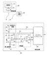
- FIG. 5 is a configuration diagram of a visible light communication system including the receiving device 50 according to the second embodiment.
- FIG. 6 is a flowchart showing processing steps of the microcomputer 53.
- 7A to 7D are waveform diagrams for explaining the operation of the receiving device 50.
- the receiving device 50 according to the second embodiment is a case where the illuminating device 20 having a weak light amount is used as compared with the disturbance light source 55 having a large light amount while avoiding the influence of the disturbance light source 55 such as sunlight or a fluorescent lamp. Even if it exists, identification ID information can be detected accurately.
- the visible light communication system includes an illumination device 20 and a reception device 50.
- the illuminating device 20 is an example of a visible light communication device (visible light transmitting device), and is the same as the illuminating device 20 described in the first embodiment, and thus detailed description thereof is omitted.
- the receiving device 50 includes a first conversion unit 51, an amplification unit 52, and a microcomputer 53. Since the microcomputer 53 is the same as the microcomputer 13 shown in the first embodiment, detailed description thereof is omitted.
- the first converter 51 includes a light receiving element 61 that converts visible light such as illumination light or disturbance light into an electrical signal, an amplifier including a resistor 62, an operational amplifier 63, and a DC power supply 64, and a current injection circuit 81. is doing.
- the first converter 51 generates a voltage signal Jm proportional to the absorption current of the light receiving element 61 by an amplifier (resistor 62, operational amplifier 63 and DC power supply 64).
- Visible light received by the light receiving element 61 is converted into an electrical signal.
- the visible light is illumination light or disturbance light that is strong or weak in response to a modulation signal obtained by position-modulating the identification ID information every predetermined symbol time.
- the electric signal output from the light receiving element 61 is amplified by an amplifier (resistor 62, operational amplifier 63 and DC power supply 64).
- the first converter 51 outputs a voltage signal Jm corresponding to the intensity of the illumination light received by the light receiving element 61 to the amplifier 52.
- the current injection circuit 81 includes a switch 82 and a resistor 83, and outputs a direct current from the power source Vcc to the operational amplifier 63 by closing the switch 82. Specifically, the current injection circuit 81 turns on the switch 82 in response to the shift instruction signal Pm from the microcomputer 53 and supplies a predetermined direct current to the light receiving element 61 through the resistor 83. That is, the current injection circuit 81 injects a direct current into the light receiving element 61 when the shift instruction signal Pm of the microcomputer 53 is on. When disturbance light is sunlight, the power supply Vcc is about 3V as an example.
- the switch 82 of the current injection circuit 81 is configured by an analog switch circuit or a transistor circuit.
- the amplifying unit 52 cuts the direct current component of the voltage signal Jm output from the first conversion unit 51 to the amplifying unit 12 by the capacitor 71, and fixes the alternating current component of the voltage signal Jm to a predetermined value by the resistor 72, the resistor 73, and the operational amplifier 74. Amplifies with gain (fixed Gain). Thereby, the output signal Km of the amplifying unit 52 becomes a signal obtained by amplifying the AC component of the voltage signal Jm of the first converting unit 51 with a predetermined gain (predetermined Gain).
- the high-pass filter type amplifying unit 52 is illustrated as the DC cut amplifying unit, but a band-pass type amplifying unit may be used.
- the amplifying unit 52 is not limited to the configuration that completely cuts the DC component of the voltage signal Jm, but may be configured to significantly reduce the DC component. That is, the meaning of cut in the second embodiment includes a significant reduction.
- the AC component of the amplified voltage signal Jm is output to the microcomputer 53 as the output signal Km.
- the microcomputer 53 receives the output signal Km output from the amplification unit 52 and the voltage signal Jm output from the first conversion unit 51.
- the illumination device 20 includes a drive unit 21 and an illumination unit 22.
- the drive unit 21 creates a modulated signal obtained by position-modulating the identification ID information every predetermined symbol time without using a subcarrier.
- the illumination unit 22 changes the intensity of the illumination light according to the modulation signal of the drive unit 21.
- a disturbance light source 55 that generates a strong amount of disturbance light such as sunlight or an incandescent bulb near the lighting device 20.
- FIG. 7 shows the illumination light Lm by the illuminating device 20 in the place of the light receiving element 61 of the 1st conversion part 51 of the receiver 50 with a continuous line, and shows the disturbance light Dt by the disturbance light source 55 with a dashed-dotted line.
- FIG. 7B shows a voltage signal Jmp based on the illumination light Lm with a broken line and a voltage signal Jm based on the disturbance light Dt with a solid line.
- FIG. 7C shows the amplified signal Kmp based on the illumination light Lm with a broken line and the amplified signal Km based on the disturbance light Dt with a solid line.
- (d) of FIG. 7 shows the rising point Rm and the falling point Fm.
- the horizontal axis represents time
- the vertical axis represents the intensity of each signal.
- the illumination light Lm of the illumination device 20 is composed of a strength change portion La and a constant portion Lb in the same manner as the illumination device 20 shown in the first embodiment.
- the disturbance light source 55 generates strong disturbance light Dt with little fluctuation. For this reason, the disturbance light Dt is much larger than the weak illumination light Lm of the illumination device 20.
- the disturbance light Dt of the disturbance light source 55 is about five times larger than the illumination light Lm.
- the first converter 51 of the receiving device 50 outputs a voltage signal Jm corresponding to the amount of light received by the light receiving element 61.
- FIG. 7B shows the voltage signal Jm.
- the light receiving element 61 of the first converter 51 Since the light receiving element 61 of the first converter 51 superimposes and receives the illumination light Lm of the illumination device 20 and the disturbance light Dt of the disturbance light source 55, a voltage signal Jm corresponding to the combined light quantity of both is obtained.
- the first conversion unit 51 causes circuit-like saturation, and the voltage signal Jm has an upper limit as shown by a solid line in FIG. In this state, a fixed value (upper limit voltage) is continuously output as the voltage signal Jm. Therefore, the output signal Km of the amplifying unit 52 is constant as shown by the solid line in FIG. In this case, since the rising point and the falling point cannot be detected even if the microcomputer 53 inputs the output signal Km having a constant value from the amplifying unit 52, the identification ID information of the illumination device 20 is received and demodulated. Can not.
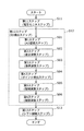
- the microcomputer 53 of the receiving device 50 executes the processing steps shown in the flowchart of FIG. This processing step will be described.
- the microcomputer 53 receives the voltage signal Jm of the first converter 51 and the eleventh step S11 which is a voltage monitoring step for turning on or off the shift instruction signal Pm according to the output voltage Jm of the first converter 51.
- the 12th step S12 which is an ID detection step
- the 13th step S13 which is a shift release step for turning off the shift instruction signal Pm after completion of the operation of at least the first step S01 (see FIG. 2B)
- the twelfth step S12 is an example of an ID detection step, and is performed after the operation of the eleventh step S11.
- the twelfth step S12 is the same as the ID detection step shown in the first embodiment, and includes the first step S01 to the sixth step S06 (see FIG. 2B, respectively).
- the microcomputer 53 first executes the eleventh step S11, and turns on the shift instruction signal Pm when the voltage signal Jm of the first converter 51 is equal to or higher than a predetermined level.
- the shift instruction signal Pm is turned on
- the switch 82 of the current injection circuit 81 of the first converter 51 is turned on (conductive), and a predetermined direct current is injected from the direct current power source Vcc to the light receiving element 61 through the resistor 83. Is done.
- the level of the direct current component of the voltage signal Jm output from the first converter 51 changes, and becomes the voltage signal Jmp indicated by the broken line in FIG.
- the DC voltage corresponding to the disturbance light Dt is canceled out by the DC current output from the current injection circuit 81, and the first converter 51 receives the voltage signal Jmp including an AC component that changes in response to the illumination light Lm. Output. Accordingly, the amplifying unit 52 outputs an alternating amplified signal Kmp that changes in response to the illumination light Lm to the microcomputer 53.
- the microcomputer 53 detects the identification ID information of the illumination device 20 in the twelfth step S12 when the output signal Kmp of the amplification unit 52 is input.
- the microcomputer 53 After executing the twelfth step S12, in the thirteenth step S13, the microcomputer 53 turns off the shift instruction signal Pm. As a result, the current injection circuit 81 turns off the switch 82 in response to the shift instruction signal Pm and releases the current injection to the light receiving element 61. Thereby, even if disturbance light is reduced or disappeared at the time of the next identification ID information detection, the identification ID information of the illuminating device 20 can be detected accurately.
- the shift instruction signal Pm may be turned off after the operation of the first step S01, and in order of the second step S02 to the sixth step S06 (respectively, see FIG. 2B) in the twelfth step S12. Can be replaced.
- the DC voltage corresponding to the disturbance light Dt can be obtained by providing the current injection circuit 81. It can be canceled by the direct current output from the current injection circuit 81. Thereby, the 1st conversion part 51 can output the voltage signal Jmp containing the alternating current part which changes in response to the illumination light Lm.
- FIG. 8 is a configuration diagram of a position information providing system including a mobile terminal to which a visible light receiving device according to the third embodiment is connected.
- the receiving device 50 according to the second embodiment is used as a visible light receiving device.
- the visible light receiving apparatus is not limited to the receiving apparatus 50 according to the second embodiment described above, but may be the receiving apparatus 10 according to the first embodiment described above.
- the modularized receiving device 50 is attached to the portable terminal 95 via the communication connection unit 92.
- the mobile terminal 95 is integrated with the receiving device 50.
- a light receiving element (not shown) of the receiving device 50 receives visible light illumination collected by the lens 91 and detects a visible light illumination device within a predetermined solid angle.
- the communication connection unit 92 is, for example, a USB unit that performs USB (Universal Serial Bus) communication.
- the receiving device 50 transmits the identification ID information of the lighting device 20 to the portable terminal 95 through the communication connection unit 92.
- the mobile terminal 95 is, for example, a mobile phone such as a smartphone or a tablet PC, and inquires the position information server 96 about the transmitted identification ID information of the lighting device 20.
- the server 96 which is an example of a location information server, returns location information corresponding to the inquired identification ID information to the mobile terminal 95. Based on the reply information from the server 96, the portable terminal 95 displays the position on the map corresponding to the identification ID information on the screen.
- the user can easily know his / her position in the underground shopping center or the building by using the receiving device 50 that can be attached to the portable terminal 95.
- the receiving device 50 according to the third embodiment can detect the identification ID information of the lighting device 20 stably and quickly, it can be used even when the user is walking.
- the communication connection unit 92 that connects the receiving device 50 and the portable terminal 95 is not limited to the USB unit, but uses a serial communication unit (RS-232C), a wireless communication unit (Bluetooth (registered trademark), Wi-Fi), or the like. May be.
- the visible light communication system including the above-described receiving device has been described using the portable terminal 95 as an example.
- the receiving device can detect the identification ID information of the lighting device 20 stably, quickly and easily. Therefore, it can be used even when the user is walking.
- the visible light receiving apparatus and visible light receiving method of the present invention can detect identification ID information of a visible light luminaire, and are useful for detecting the position of a portable terminal in an underground shopping center or a building.
Abstract
Description
図1は、実施の形態1にかかる受信装置10を含む可視光通信システムの構成図である。受信装置10は、可視光受信装置の一例である。図2Aは、実施の形態1にかかるマイクロコンピュータ13の構成図である。マイクロコンピュータ13は、処理部の一例である。図2Bは、マイクロコンピュータ13の処理ステップを示すフローチャートである。図3の(a)~(d)は、受信装置10の動作を説明するための波形図である。 (Embodiment 1)
FIG. 1 is a configuration diagram of a visible light communication system including the receiving
以下に、実施の形態1の変形例について説明する。図4の(a)~(d)は、本変形例にかかる可視光受信装置の動作を説明する波形図である。 (Modification of Embodiment 1)
Below, the modification of
次に、本発明の実施の形態2について説明する。 (Embodiment 2)
Next, a second embodiment of the present invention will be described.
次に、本発明の実施の形態3について説明する。本実施の形態3にかかる可視光受信装置を用いた位置情報システムについて、図8を参照して説明する。図8は、本実施の形態3にかかる可視光受信装置を接続した携帯端末を含む位置情報提供システムの構成図である。本実施の形態3では、可視光受信装置として実施の形態2にかかる受信装置50を用いた場合について説明する。なお、可視光受信装置は、前述の実施の形態2にかかる受信装置50に限らず、前述の実施の形態1にかかる受信装置10であってもよい。 (Embodiment 3)
Next, a third embodiment of the present invention will be described. A position information system using the visible light receiving apparatus according to the third embodiment will be described with reference to FIG. FIG. 8 is a configuration diagram of a position information providing system including a mobile terminal to which a visible light receiving device according to the third embodiment is connected. In the third embodiment, a case where the receiving
11、51 第1変換部
12、52 増幅部
13、53 マイクロコンピュータ
14 第2変換部
15 第1演算部
16 第2演算部
17 検出部
18 第3演算部
19 第4演算部
20 照明装置
21 駆動部
22 照明部
25、55 外乱光源
61、133 受光素子
62、72、73、83 抵抗
63、74 オペアンプ
64 直流電源
71 コンデンサ
81 電流注入回路
82 スイッチ
95 携帯端末
96 位置情報サーバ
100 可視光通信システム
110 送信装置
130 受信装置
136 AGC DESCRIPTION OF
Claims (12)
- シンボル時間毎に位置変調した変調信号に応じて強弱変化する可視光を受光し、前記可視光の受光光量に応じた電圧信号を出力する第1変換部と、
前記電圧信号に含まれる直流分をカットすると共に交流分を増幅して出力する増幅部と、
前記増幅部から出力された電圧信号を処理して、前記変調信号に対応する復調信号を出力する処理部と、を具備し、
前記処理部は、
サンプリング時間毎に、前記増幅部から出力された前記電圧信号をAD変換値にAD変換する第2変換部と、
複数の前記AD変換値を用いた差分演算により、差分デジタル値を算出する第1演算部と、
複数個の前記差分デジタル値のピーク値に応じた+側基準値と-側基準値とを算出する第2演算部と、
前記差分デジタル値が前記+側基準値よりも大きくなる立上ポイントと、前記差分デジタル値が前記-側基準値よりも小さくなる立下ポイントとを検出する検出部と、
前記立上ポイントと該立上ポイントの直後に検出される前記立下ポイントとの間の第1サンプル期間と、前記立下ポイントと該立下ポイントの直後に検出される立上ポイントとの間の第2サンプル期間と、を算出する第3演算部と、
時系列的に交互に生じる前記第1サンプル期間と前記第2サンプル期間とに基づいて、前記シンボル時間毎の前記復調信号を算出する第4演算部と、を有する、
可視光受信装置。 A first converter that receives visible light that changes in intensity according to a modulation signal that is position-modulated for each symbol time, and outputs a voltage signal corresponding to the amount of received light of the visible light;
An amplifying unit that cuts a DC component included in the voltage signal and amplifies and outputs the AC component;
A processing unit that processes the voltage signal output from the amplification unit and outputs a demodulated signal corresponding to the modulation signal; and
The processor is
A second conversion unit that AD converts the voltage signal output from the amplification unit into an AD conversion value at each sampling time;
A first calculation unit that calculates a difference digital value by a difference calculation using a plurality of the AD conversion values;
A second calculation unit that calculates a + side reference value and a − side reference value according to the peak values of the plurality of difference digital values;
A detection unit for detecting a rising point at which the difference digital value is larger than the + side reference value and a falling point at which the difference digital value is smaller than the − side reference value;
A first sample period between the rising point and the falling point detected immediately after the rising point, and between the falling point and a rising point detected immediately after the falling point A second calculation period, a third calculation unit for calculating,
A fourth arithmetic unit that calculates the demodulated signal for each symbol time based on the first sample period and the second sample period that occur alternately in time series,
Visible light receiver. - 前記第1変換部は、さらに、
前記処理部から出力されるシフト指示信号に基づいてオン又はオフとなる回路を備え、
前記処理部は、
前記第2変換部によるAD変換を実行する前に、前記回路をオンにするシフト指示信号を出力し、
少なくとも前記AD変換を実行した後に、前記回路をオフにするシフト指示信号を出力する、
請求項1に記載の可視光受信装置。 The first conversion unit further includes:
A circuit that is turned on or off based on a shift instruction signal output from the processing unit,
The processor is
Before performing AD conversion by the second conversion unit, output a shift instruction signal to turn on the circuit,
Outputting a shift instruction signal for turning off the circuit after performing at least the AD conversion;
The visible light receiving device according to claim 1. - 前記第2演算部は、前記差分デジタル値のピーク値の最大値または平均値に比例した+側基準値および-側基準値を算出する、
請求項1または2に記載の可視光受信装置。 The second calculation unit calculates a + side reference value and a-side reference value proportional to a maximum value or an average value of the peak values of the difference digital values;
The visible light receiving device according to claim 1. - 前記検出部は、2個の立下ポイントが時系列的に連続した場合に、連続する2個の前記立下ポイントのうちの2番目の立下ポイントおよび前記2番目の立下ポイントに後続する立上ポイントを、検出対象から除外する、
請求項1から3のいずれか1項に記載の可視光受信装置。 When the two falling points are consecutive in time series, the detection unit follows the second falling point and the second falling point of the two consecutive falling points. Exclude the start point from detection,
The visible light receiver according to any one of claims 1 to 3. - 前記検出部は、2個の立上ポイントが時系列的に連続した場合に、連続する2個の前記立上ポイントのうちの2番目の立上ポイントおよび前記2番目の立上ポイントに後続する立下ポイントを、検出対象から除外する、
請求項1から3のいずれか1項に記載の可視光受信装置。 When the two rising points are consecutive in time series, the detection unit follows the second rising point and the second rising point among the two consecutive rising points. Excluding falling points from detection,
The visible light receiver according to any one of claims 1 to 3. - 前記検出部は、
2個の立下ポイントが時系列的に連続した場合に、連続する2個の前記立下ポイントのうちの1番目の立下ポイントの直前または2番目の立下ポイントの直後の立上ポイントから、前記1番目の立下ポイントまでの前記第1サンプル期間および該立上ポイントから前記2番目の立下ポイントまでの前記第2サンプル期間を計測し、
前記第1サンプル期間および前記第2サンプル期間のうちスロット時間の整数倍の長さの時間に近い側の一方の立下ポイントを検出すると共に、他方の立下ポイントを検出対象から除外する、
請求項1から3のいずれか1項に記載の可視光受信装置。 The detector is
When two falling points are consecutive in time series, from the rising point immediately before the first falling point or immediately after the second falling point of the two consecutive falling points. Measuring the first sample period to the first falling point and the second sample period from the rising point to the second falling point;
Detecting one falling point on the side of the first sample period and the second sample period that is closer to an integral multiple of the slot time, and excluding the other falling point from the detection target;
The visible light receiver according to any one of claims 1 to 3. - 前記検出部は、2個の立上ポイントが時系列的に連続した場合に、連続する2個の前記立上ポイントのうちの1番目の立上ポイントの直前または2番目の立上ポイントの直後の立下ポイントから、前記1番目の立上ポイントまでの前記第1サンプル期間および該立下ポイントから前記2番目の立上ポイントまでの前記第2サンプル期間を計測し、
前記第1サンプル期間および前記第2サンプル期間のうちスロット時間の整数倍の長さの時間に近い側の一方の立上ポイントを検出すると共に、他方の立上ポイントを検出対象から除外する、
請求項1から3のいずれか1項に記載の可視光受信装置。 When the two rising points are consecutive in time series, the detecting unit immediately before the first rising point or immediately after the second rising point among the two consecutive rising points. Measuring the first sample period from the falling point to the first rising point and the second sample period from the falling point to the second rising point;
Detecting one rising point on the side of the first sample period and the second sample period that is close to a time that is an integral multiple of the slot time, and excluding the other rising point from the detection target;
The visible light receiver according to any one of claims 1 to 3. - 前記第1演算部は、一のサンプリング時点の前記AD変換値と該一のサンプリング時点から2サンプリング間隔以上離れた他のサンプリング時点の前記AD変換値とを差分演算して前記差分デジタル値を算出し、
前記サンプリング時間を前記シンボル時間の1/12以下にする、
請求項1から7のいずれか1項に記載の可視光受信装置。 The first calculation unit calculates the difference digital value by calculating a difference between the AD conversion value at one sampling time point and the AD conversion value at another sampling time point separated from the one sampling time point by two sampling intervals or more. And
Making the sampling time less than 1/12 of the symbol time;
The visible light receiver according to any one of claims 1 to 7. - 請求項1から8のいずれか1項に記載の可視光受信装置と、
可視光送信装置と、から構成された、
可視光通信システム。 The visible light receiving device according to any one of claims 1 to 8,
A visible light transmitter, and
Visible light communication system. - 請求項1から8のいずれか1項に記載の可視光受信装置を内蔵した、
携帯端末。 The visible light receiving device according to claim 1 is incorporated.
Mobile device. - 可視光に含まれる情報を取得する可視光受信方法であって、
前記可視光受信方法は、
受光した可視光に応じた電圧信号を、第1変換部によりサンプリング時間毎にAD変換値にAD変換する第1ステップと、
複数の前記AD変換値を用いた差分演算により、差分デジタル値を算出する第2ステップと、
複数の前記差分デジタル値のピーク値に応じた+側基準値と-側基準値とを算出する第3ステップと、
前記差分デジタル値が前記+側基準値よりも大きくなる立上ポイントと、前記差分デジタル値が前記-側基準値よりも小さくなる立下ポイントと、を検出する第4ステップと、
前記立上ポイントと該立上ポイントの直後に検出される前記立下ポイントとの間の第1サンプル期間と、前記立下ポイントと該立下ポイントの直後に検出される立上ポイントとの間の第2サンプル期間と、を算出する第5ステップと、
時系列的に交互に生じる前記第1サンプル期間と前記第2サンプル期間とに基づいて、シンボル時間毎の前記電圧信号に対応する復調信号を算出する第6ステップと、を含む、
可視光受信方法。 A visible light receiving method for acquiring information contained in visible light,
The visible light receiving method is:
A first step of AD converting a voltage signal corresponding to the received visible light into an AD conversion value for each sampling time by the first converter;
A second step of calculating a difference digital value by a difference calculation using the plurality of AD conversion values;
A third step of calculating a + side reference value and a − side reference value according to the peak values of the plurality of difference digital values;
A fourth step of detecting a rising point at which the difference digital value is larger than the + side reference value and a falling point at which the difference digital value is smaller than the − side reference value;
A first sample period between the rising point and the falling point detected immediately after the rising point, and between the falling point and a rising point detected immediately after the falling point A second step of calculating a second sample period of
A sixth step of calculating a demodulated signal corresponding to the voltage signal for each symbol time based on the first sample period and the second sample period that occur alternately in time series,
Visible light receiving method. - 前記可視光受信方法は、さらに、
前記第1ステップを実行する前に、回路をオンにするシフト指示信号を出力する第11モニタステップを含み、
少なくとも前記第11を実行した後に、前記回路をオフ支持にするシフト指示信号を出力する第13ステップを含む、
請求項11に記載の可視光受信方法。 The visible light receiving method further includes:
An eleventh monitoring step of outputting a shift instruction signal for turning on the circuit before executing the first step;
Including a thirteenth step of outputting a shift instruction signal for supporting the circuit off after performing at least the eleventh.
The visible light receiving method according to claim 11.
Priority Applications (4)
| Application Number | Priority Date | Filing Date | Title |
|---|---|---|---|
| US14/118,930 US9077456B2 (en) | 2012-04-03 | 2013-03-06 | Visible light receiving device and visible light receiving method |
| JP2013534097A JP5834188B2 (en) | 2012-04-03 | 2013-03-06 | Visible light receiving apparatus and visible light receiving method |
| EP13773145.1A EP2835916B1 (en) | 2012-04-03 | 2013-03-06 | Visible light reception device and visible light reception method |
| CN201380001411.6A CN103548288B (en) | 2012-04-03 | 2013-03-06 | Visible optical pickup apparatus and visible ray method of reseptance |
Applications Claiming Priority (2)
| Application Number | Priority Date | Filing Date | Title |
|---|---|---|---|
| JP2012-084552 | 2012-04-03 | ||
| JP2012084552 | 2012-04-03 |
Publications (1)
| Publication Number | Publication Date |
|---|---|
| WO2013150716A1 true WO2013150716A1 (en) | 2013-10-10 |
Family
ID=49300225
Family Applications (1)
| Application Number | Title | Priority Date | Filing Date |
|---|---|---|---|
| PCT/JP2013/001397 WO2013150716A1 (en) | 2012-04-03 | 2013-03-06 | Visible light reception device and visible light reception method |
Country Status (5)
| Country | Link |
|---|---|
| US (1) | US9077456B2 (en) |
| EP (1) | EP2835916B1 (en) |
| JP (1) | JP5834188B2 (en) |
| CN (1) | CN103548288B (en) |
| WO (1) | WO2013150716A1 (en) |
Cited By (4)
| Publication number | Priority date | Publication date | Assignee | Title |
|---|---|---|---|---|
| JP2016005231A (en) * | 2014-06-19 | 2016-01-12 | ルネサスエレクトロニクス株式会社 | Optical receiver |
| JP2018046585A (en) * | 2017-12-27 | 2018-03-22 | ルネサスエレクトロニクス株式会社 | Optical receiver |
| JP2020137033A (en) * | 2019-02-25 | 2020-08-31 | 国立大学法人信州大学 | Visible light communication processing system and portable terminal for visible light communication |
| CN112260672A (en) * | 2020-10-19 | 2021-01-22 | 深圳市太美亚电子科技有限公司 | Method for adjusting induction distance of infrared device |
Families Citing this family (8)
| Publication number | Priority date | Publication date | Assignee | Title |
|---|---|---|---|---|
| CN103548288B (en) * | 2012-04-03 | 2016-08-17 | 松下知识产权经营株式会社 | Visible optical pickup apparatus and visible ray method of reseptance |
| US9755741B1 (en) * | 2014-01-28 | 2017-09-05 | Cooper Technologies Company | Visible-light based communication and occupancy detection |
| US9735868B2 (en) * | 2014-07-23 | 2017-08-15 | Qualcomm Incorporated | Derivation of an identifier encoded in a visible light communication signal |
| JP6366015B2 (en) * | 2014-07-30 | 2018-08-01 | パナソニックIpマネジメント株式会社 | Visible light communication system |
| CN105827316A (en) * | 2016-05-24 | 2016-08-03 | 清华大学 | Visible light communications method and apparatus for suppressing inter-lamp interference |
| KR102351498B1 (en) * | 2018-01-09 | 2022-01-14 | 삼성전자주식회사 | Data processing method and electronic apparatus thereof |
| US11333765B2 (en) * | 2018-05-17 | 2022-05-17 | Samsung Electronics Co., Ltd. | Distance measuring device and method |
| CN109617602B (en) * | 2018-12-03 | 2020-07-24 | 清华大学深圳研究生院 | Link interference suppression method and device, electronic equipment and storage medium |
Citations (5)
| Publication number | Priority date | Publication date | Assignee | Title |
|---|---|---|---|---|
| JP2001512918A (en) * | 1997-08-04 | 2001-08-28 | モトローラ・インコーポレイテッド | Laser communication method and device in lossy medium |
| JP2007097071A (en) | 2005-09-30 | 2007-04-12 | Nec Corp | Visible light controller, visible light control circuit, visible light communication equipment and visible light control method |
| JP2008104020A (en) * | 2006-10-19 | 2008-05-01 | Matsushita Electric Works Ltd | Light transmission system |
| JP2008193701A (en) * | 2007-02-06 | 2008-08-21 | Oerlikon Space Ag | Optical high-rate pulse position modulation scheme and optical communication system based thereon |
| JP2010239350A (en) | 2009-03-31 | 2010-10-21 | Comtech 2000:Kk | Visible light communication system, and transmitter and receiver of the same |
Family Cites Families (27)
| Publication number | Priority date | Publication date | Assignee | Title |
|---|---|---|---|---|
| JP3224181B2 (en) * | 1993-11-09 | 2001-10-29 | 富士通株式会社 | Data reproduction system from optical disk |
| US5926301A (en) | 1994-02-28 | 1999-07-20 | International Business Machines Corporation | Method and apparatus for optical wireless communication |
| SE9400824D0 (en) | 1994-03-10 | 1994-03-10 | Siemens Elema Ab | Optical transmission device |
| JP3207134B2 (en) * | 1997-05-16 | 2001-09-10 | 株式会社小糸製作所 | Lighting circuit of discharge lamp |
| US6038021A (en) * | 1997-12-11 | 2000-03-14 | Scientific Technologies, Inc. | Optically based on-line fiber monitoring system with drift compensation |
| JP4207490B2 (en) | 2002-08-06 | 2009-01-14 | ソニー株式会社 | Optical communication device, optical communication data output method, optical communication data analysis method, and computer program |
| US7289560B2 (en) | 2003-01-17 | 2007-10-30 | Freesystems Pte. Ltd. | Digital modulation and demodulation technique for reliable wireless (both RF and IR) and wired high bandwidth data transmission |
| CN200959600Y (en) * | 2006-05-30 | 2007-10-10 | 中国计量学院 | Low-noise wide-band photoelectric receiver with automatic gain control |
| JP2008154063A (en) | 2006-12-19 | 2008-07-03 | Tamura Seisakusho Co Ltd | Portable illuminator with visible light communication function and information communication system |
| JP2008167303A (en) | 2006-12-28 | 2008-07-17 | Fujitsu Ltd | Data sampling circuit and data sampling method |
| JP5031427B2 (en) * | 2007-03-30 | 2012-09-19 | 三星電子株式会社 | Visible light transmitter, visible light receiver, visible light communication system, and visible light communication method |
| JP4538508B2 (en) | 2007-11-08 | 2010-09-08 | シャープ株式会社 | Receiver, electronic device |
| US8050572B2 (en) | 2007-05-29 | 2011-11-01 | Sharp Kabushiki Kaisha | Receiver and electronic device |
| KR101307610B1 (en) | 2007-08-10 | 2013-09-12 | 삼성전자주식회사 | Method and apparatus for processing signals of photodetector in visible light communication |
| US7746256B2 (en) * | 2007-10-05 | 2010-06-29 | Infineon Technologies Ag | Analog to digital conversion using irregular sampling |
| JP4929126B2 (en) | 2007-11-06 | 2012-05-09 | 株式会社東芝 | Visible light communication system |
| KR101365348B1 (en) * | 2007-12-18 | 2014-02-21 | 삼성전자주식회사 | Message exchanging method in navigation system using visible light communication |
| JP2009219074A (en) | 2008-03-12 | 2009-09-24 | Taiyo Yuden Co Ltd | Visible light communication method and apparatus therefor |
| JP5171393B2 (en) | 2008-05-27 | 2013-03-27 | パナソニック株式会社 | Visible light communication system |
| JP4564559B2 (en) * | 2008-10-20 | 2010-10-20 | 株式会社半導体理工学研究センター | Differential amplifier circuit and AD converter using the same |
| EP2219307B1 (en) * | 2009-02-16 | 2013-10-02 | Kabushiki Kaisha Toshiba | Apparatus for transmitting and receiving a signal in a visible light communication system |
| US8165472B2 (en) * | 2009-02-19 | 2012-04-24 | Kabushiki Kaisha Toshiba | Apparatus for transmitting and receiving a signal in a visible light communication system |
| KR101621095B1 (en) | 2009-09-16 | 2016-05-16 | 삼성전자주식회사 | Method and apparatus for transmitting additional information through display |
| US8097853B2 (en) * | 2009-11-17 | 2012-01-17 | Dialog Semiconductor Gmbh | Infrared photocurrent front-end ADC for rain-sensing system with ambient light compensation |
| JP5554675B2 (en) * | 2010-09-29 | 2014-07-23 | 富士通株式会社 | Successive comparison A / D converter |
| US8804101B2 (en) * | 2012-03-16 | 2014-08-12 | Advanced Scientific Concepts, Inc. | Personal LADAR sensor |
| CN103548288B (en) * | 2012-04-03 | 2016-08-17 | 松下知识产权经营株式会社 | Visible optical pickup apparatus and visible ray method of reseptance |
-
2013
- 2013-03-06 CN CN201380001411.6A patent/CN103548288B/en active Active
- 2013-03-06 US US14/118,930 patent/US9077456B2/en active Active
- 2013-03-06 WO PCT/JP2013/001397 patent/WO2013150716A1/en active Application Filing
- 2013-03-06 JP JP2013534097A patent/JP5834188B2/en active Active
- 2013-03-06 EP EP13773145.1A patent/EP2835916B1/en active Active
Patent Citations (5)
| Publication number | Priority date | Publication date | Assignee | Title |
|---|---|---|---|---|
| JP2001512918A (en) * | 1997-08-04 | 2001-08-28 | モトローラ・インコーポレイテッド | Laser communication method and device in lossy medium |
| JP2007097071A (en) | 2005-09-30 | 2007-04-12 | Nec Corp | Visible light controller, visible light control circuit, visible light communication equipment and visible light control method |
| JP2008104020A (en) * | 2006-10-19 | 2008-05-01 | Matsushita Electric Works Ltd | Light transmission system |
| JP2008193701A (en) * | 2007-02-06 | 2008-08-21 | Oerlikon Space Ag | Optical high-rate pulse position modulation scheme and optical communication system based thereon |
| JP2010239350A (en) | 2009-03-31 | 2010-10-21 | Comtech 2000:Kk | Visible light communication system, and transmitter and receiver of the same |
Cited By (6)
| Publication number | Priority date | Publication date | Assignee | Title |
|---|---|---|---|---|
| JP2016005231A (en) * | 2014-06-19 | 2016-01-12 | ルネサスエレクトロニクス株式会社 | Optical receiver |
| TWI650963B (en) * | 2014-06-19 | 2019-02-11 | 日商瑞薩電子股份有限公司 | Optical receiver |
| JP2018046585A (en) * | 2017-12-27 | 2018-03-22 | ルネサスエレクトロニクス株式会社 | Optical receiver |
| JP2020137033A (en) * | 2019-02-25 | 2020-08-31 | 国立大学法人信州大学 | Visible light communication processing system and portable terminal for visible light communication |
| CN112260672A (en) * | 2020-10-19 | 2021-01-22 | 深圳市太美亚电子科技有限公司 | Method for adjusting induction distance of infrared device |
| CN112260672B (en) * | 2020-10-19 | 2024-02-06 | 深圳市太美亚电子科技有限公司 | Method for adjusting induction distance of infrared device |
Also Published As
| Publication number | Publication date |
|---|---|
| EP2835916B1 (en) | 2018-10-10 |
| US20140093254A1 (en) | 2014-04-03 |
| JPWO2013150716A1 (en) | 2015-12-17 |
| US9077456B2 (en) | 2015-07-07 |
| EP2835916A1 (en) | 2015-02-11 |
| EP2835916A4 (en) | 2015-04-01 |
| CN103548288A (en) | 2014-01-29 |
| CN103548288B (en) | 2016-08-17 |
| JP5834188B2 (en) | 2015-12-16 |
Similar Documents
| Publication | Publication Date | Title |
|---|---|---|
| JP5834188B2 (en) | Visible light receiving apparatus and visible light receiving method | |
| KR101558060B1 (en) | Indoor positioning system based on visible light communication, method, system, server and electronic device for indoor navigation | |
| US10250328B2 (en) | Positioning system based on visible light communications | |
| CN110383715B (en) | Power optimization in visible light communication positioning | |
| WO2010145722A1 (en) | Mobile device for receiving modulated light and apparatus for transmitting information as well as system comprising the mobile device and the apparatus and corresponding methods | |
| DE602007009813D1 (en) | WLAN RECEIVER AND CORRESPONDING METHOD | |
| RU2012102008A (en) | IMPROVED DETECTION USING TRANSMISSION NOTIFICATIONS | |
| US10077985B2 (en) | Wireless positioning system, wireless positioning terminal, and point information transmitter | |
| JP2014168137A (en) | Visible light communication system | |
| ATE467276T1 (en) | DETECTION OF THE PRESENCE OF SPREAD SPECTRUM SIGNALS | |
| Yoshizawa et al. | A simple but effective approach for visible light beacon-based positioning systems with smartphone | |
| Mai et al. | Implementation and evaluation of VLC-based indoor positioning systems for smart supermarkets | |
| JP5641951B2 (en) | Wireless communication system, wireless communication method, wireless device, and data transmitter | |
| JP2017064115A (en) | Biological body measurement device and biological body measurement system | |
| KR101580407B1 (en) | An apparatus and a method for VLC | |
| JP2013005327A (en) | Optical receiver | |
| JP6615587B2 (en) | Position determining program, position determining method, and position determining apparatus | |
| KR101647948B1 (en) | A position tracking system, a position tracking apparatus and a position tracking method for a user device using visible light communication | |
| CN203616338U (en) | Phase sensitive modulation-type photoelectric speed sensor | |
| JP6907482B2 (en) | Communication terminals, control devices, communication methods, control methods, and programs | |
| KR101576746B1 (en) | An apparatus and a method for VLC | |
| JP2015507751A (en) | Photodetector | |
| MY181662A (en) | A system and method to extract phase shift of a fluorescence signal | |
| JP2015136102A (en) | remote control transmitter, remote control receiver, pointing device, and pointing method | |
| Raes et al. | Experimental evaluation of the precision of received signal strength based visible light positioning |
Legal Events
| Date | Code | Title | Description |
|---|---|---|---|
| ENP | Entry into the national phase |
Ref document number: 2013534097 Country of ref document: JP Kind code of ref document: A |
|
| WWE | Wipo information: entry into national phase |
Ref document number: 2013773145 Country of ref document: EP |
|
| WWE | Wipo information: entry into national phase |
Ref document number: 14118930 Country of ref document: US |
|
| 121 | Ep: the epo has been informed by wipo that ep was designated in this application |
Ref document number: 13773145 Country of ref document: EP Kind code of ref document: A1 |
|
| NENP | Non-entry into the national phase |
Ref country code: DE |