EP2321702B1 - Exposure apparatus and methods - Google Patents
Exposure apparatus and methods Download PDFInfo
- Publication number
- EP2321702B1 EP2321702B1 EP09785419.4A EP09785419A EP2321702B1 EP 2321702 B1 EP2321702 B1 EP 2321702B1 EP 09785419 A EP09785419 A EP 09785419A EP 2321702 B1 EP2321702 B1 EP 2321702B1
- Authority
- EP
- European Patent Office
- Prior art keywords
- cgh
- substrate
- exposure apparatus
- computer generated
- generated hologram
- Prior art date
- Legal status (The legal status is an assumption and is not a legal conclusion. Google has not performed a legal analysis and makes no representation as to the accuracy of the status listed.)
- Not-in-force
Links
- 238000000034 method Methods 0.000 title claims description 50
- 239000000758 substrate Substances 0.000 claims description 58
- 238000000059 patterning Methods 0.000 claims description 18
- 230000005855 radiation Effects 0.000 claims description 9
- 238000012876 topography Methods 0.000 claims description 8
- 230000001427 coherent effect Effects 0.000 claims description 7
- 238000001093 holography Methods 0.000 claims description 6
- 238000007689 inspection Methods 0.000 claims description 2
- 238000003384 imaging method Methods 0.000 abstract description 9
- 238000013461 design Methods 0.000 abstract description 6
- 238000004422 calculation algorithm Methods 0.000 abstract description 4
- 238000000206 photolithography Methods 0.000 abstract description 4
- 238000005286 illumination Methods 0.000 description 16
- 238000001459 lithography Methods 0.000 description 16
- 230000003287 optical effect Effects 0.000 description 14
- 238000013459 approach Methods 0.000 description 12
- 238000004519 manufacturing process Methods 0.000 description 10
- 229920002120 photoresistant polymer Polymers 0.000 description 9
- 230000008569 process Effects 0.000 description 9
- 230000009467 reduction Effects 0.000 description 9
- 238000003491 array Methods 0.000 description 8
- 238000011161 development Methods 0.000 description 6
- 230000018109 developmental process Effects 0.000 description 6
- 238000005516 engineering process Methods 0.000 description 6
- 229910052710 silicon Inorganic materials 0.000 description 5
- 239000010703 silicon Substances 0.000 description 5
- 235000012431 wafers Nutrition 0.000 description 5
- XUIMIQQOPSSXEZ-UHFFFAOYSA-N Silicon Chemical compound [Si] XUIMIQQOPSSXEZ-UHFFFAOYSA-N 0.000 description 4
- 238000004364 calculation method Methods 0.000 description 4
- 230000000694 effects Effects 0.000 description 4
- IOYNQIMAUDJVEI-BMVIKAAMSA-N Tepraloxydim Chemical group C1C(=O)C(C(=N/OC\C=C\Cl)/CC)=C(O)CC1C1CCOCC1 IOYNQIMAUDJVEI-BMVIKAAMSA-N 0.000 description 3
- 238000009826 distribution Methods 0.000 description 3
- 238000005530 etching Methods 0.000 description 3
- 238000009472 formulation Methods 0.000 description 3
- 238000004377 microelectronic Methods 0.000 description 3
- 239000000203 mixture Substances 0.000 description 3
- 238000012986 modification Methods 0.000 description 3
- 230000004048 modification Effects 0.000 description 3
- 238000004806 packaging method and process Methods 0.000 description 3
- 239000003990 capacitor Substances 0.000 description 2
- 238000013500 data storage Methods 0.000 description 2
- 230000001419 dependent effect Effects 0.000 description 2
- 230000008021 deposition Effects 0.000 description 2
- 239000004973 liquid crystal related substance Substances 0.000 description 2
- 230000004807 localization Effects 0.000 description 2
- 238000007639 printing Methods 0.000 description 2
- 238000004886 process control Methods 0.000 description 2
- 238000011160 research Methods 0.000 description 2
- 239000004065 semiconductor Substances 0.000 description 2
- 238000000926 separation method Methods 0.000 description 2
- 238000001228 spectrum Methods 0.000 description 2
- 240000005589 Calophyllum inophyllum Species 0.000 description 1
- VYZAMTAEIAYCRO-UHFFFAOYSA-N Chromium Chemical compound [Cr] VYZAMTAEIAYCRO-UHFFFAOYSA-N 0.000 description 1
- 230000003044 adaptive effect Effects 0.000 description 1
- 230000004075 alteration Effects 0.000 description 1
- 238000011953 bioanalysis Methods 0.000 description 1
- 230000015556 catabolic process Effects 0.000 description 1
- 230000008859 change Effects 0.000 description 1
- 238000012512 characterization method Methods 0.000 description 1
- 239000011248 coating agent Substances 0.000 description 1
- 238000000576 coating method Methods 0.000 description 1
- 230000000052 comparative effect Effects 0.000 description 1
- 238000012937 correction Methods 0.000 description 1
- 238000006731 degradation reaction Methods 0.000 description 1
- 238000005553 drilling Methods 0.000 description 1
- 238000010291 electrical method Methods 0.000 description 1
- 238000009713 electroplating Methods 0.000 description 1
- 230000005284 excitation Effects 0.000 description 1
- 238000013213 extrapolation Methods 0.000 description 1
- 230000006870 function Effects 0.000 description 1
- 239000011521 glass Substances 0.000 description 1
- 239000002241 glass-ceramic Substances 0.000 description 1
- 238000000025 interference lithography Methods 0.000 description 1
- 239000000463 material Substances 0.000 description 1
- 238000007620 mathematical function Methods 0.000 description 1
- 238000005259 measurement Methods 0.000 description 1
- QSHDDOUJBYECFT-UHFFFAOYSA-N mercury Chemical compound [Hg] QSHDDOUJBYECFT-UHFFFAOYSA-N 0.000 description 1
- 229910052753 mercury Inorganic materials 0.000 description 1
- 238000000386 microscopy Methods 0.000 description 1
- 210000002569 neuron Anatomy 0.000 description 1
- 238000012576 optical tweezer Methods 0.000 description 1
- 238000002360 preparation method Methods 0.000 description 1
- 238000011084 recovery Methods 0.000 description 1
- 230000002787 reinforcement Effects 0.000 description 1
- 230000004044 response Effects 0.000 description 1
- 238000010561 standard procedure Methods 0.000 description 1
- 230000001629 suppression Effects 0.000 description 1
- 230000001131 transforming effect Effects 0.000 description 1
- 210000003462 vein Anatomy 0.000 description 1
- 238000007704 wet chemistry method Methods 0.000 description 1
Images
Classifications
-
- G—PHYSICS
- G03—PHOTOGRAPHY; CINEMATOGRAPHY; ANALOGOUS TECHNIQUES USING WAVES OTHER THAN OPTICAL WAVES; ELECTROGRAPHY; HOLOGRAPHY
- G03F—PHOTOMECHANICAL PRODUCTION OF TEXTURED OR PATTERNED SURFACES, e.g. FOR PRINTING, FOR PROCESSING OF SEMICONDUCTOR DEVICES; MATERIALS THEREFOR; ORIGINALS THEREFOR; APPARATUS SPECIALLY ADAPTED THEREFOR
- G03F7/00—Photomechanical, e.g. photolithographic, production of textured or patterned surfaces, e.g. printing surfaces; Materials therefor, e.g. comprising photoresists; Apparatus specially adapted therefor
- G03F7/70—Microphotolithographic exposure; Apparatus therefor
- G03F7/70216—Mask projection systems
- G03F7/703—Non-planar pattern areas or non-planar masks, e.g. curved masks or substrates
-
- G—PHYSICS
- G03—PHOTOGRAPHY; CINEMATOGRAPHY; ANALOGOUS TECHNIQUES USING WAVES OTHER THAN OPTICAL WAVES; ELECTROGRAPHY; HOLOGRAPHY
- G03F—PHOTOMECHANICAL PRODUCTION OF TEXTURED OR PATTERNED SURFACES, e.g. FOR PRINTING, FOR PROCESSING OF SEMICONDUCTOR DEVICES; MATERIALS THEREFOR; ORIGINALS THEREFOR; APPARATUS SPECIALLY ADAPTED THEREFOR
- G03F7/00—Photomechanical, e.g. photolithographic, production of textured or patterned surfaces, e.g. printing surfaces; Materials therefor, e.g. comprising photoresists; Apparatus specially adapted therefor
- G03F7/70—Microphotolithographic exposure; Apparatus therefor
- G03F7/70058—Mask illumination systems
- G03F7/7015—Details of optical elements
- G03F7/70158—Diffractive optical elements
-
- G—PHYSICS
- G03—PHOTOGRAPHY; CINEMATOGRAPHY; ANALOGOUS TECHNIQUES USING WAVES OTHER THAN OPTICAL WAVES; ELECTROGRAPHY; HOLOGRAPHY
- G03F—PHOTOMECHANICAL PRODUCTION OF TEXTURED OR PATTERNED SURFACES, e.g. FOR PRINTING, FOR PROCESSING OF SEMICONDUCTOR DEVICES; MATERIALS THEREFOR; ORIGINALS THEREFOR; APPARATUS SPECIALLY ADAPTED THEREFOR
- G03F7/00—Photomechanical, e.g. photolithographic, production of textured or patterned surfaces, e.g. printing surfaces; Materials therefor, e.g. comprising photoresists; Apparatus specially adapted therefor
- G03F7/70—Microphotolithographic exposure; Apparatus therefor
- G03F7/70216—Mask projection systems
- G03F7/70283—Mask effects on the imaging process
- G03F7/70291—Addressable masks, e.g. spatial light modulators [SLMs], digital micro-mirror devices [DMDs] or liquid crystal display [LCD] patterning devices
-
- G—PHYSICS
- G03—PHOTOGRAPHY; CINEMATOGRAPHY; ANALOGOUS TECHNIQUES USING WAVES OTHER THAN OPTICAL WAVES; ELECTROGRAPHY; HOLOGRAPHY
- G03F—PHOTOMECHANICAL PRODUCTION OF TEXTURED OR PATTERNED SURFACES, e.g. FOR PRINTING, FOR PROCESSING OF SEMICONDUCTOR DEVICES; MATERIALS THEREFOR; ORIGINALS THEREFOR; APPARATUS SPECIALLY ADAPTED THEREFOR
- G03F7/00—Photomechanical, e.g. photolithographic, production of textured or patterned surfaces, e.g. printing surfaces; Materials therefor, e.g. comprising photoresists; Apparatus specially adapted therefor
- G03F7/70—Microphotolithographic exposure; Apparatus therefor
- G03F7/70408—Interferometric lithography; Holographic lithography; Self-imaging lithography, e.g. utilizing the Talbot effect
-
- G—PHYSICS
- G03—PHOTOGRAPHY; CINEMATOGRAPHY; ANALOGOUS TECHNIQUES USING WAVES OTHER THAN OPTICAL WAVES; ELECTROGRAPHY; HOLOGRAPHY
- G03F—PHOTOMECHANICAL PRODUCTION OF TEXTURED OR PATTERNED SURFACES, e.g. FOR PRINTING, FOR PROCESSING OF SEMICONDUCTOR DEVICES; MATERIALS THEREFOR; ORIGINALS THEREFOR; APPARATUS SPECIALLY ADAPTED THEREFOR
- G03F7/00—Photomechanical, e.g. photolithographic, production of textured or patterned surfaces, e.g. printing surfaces; Materials therefor, e.g. comprising photoresists; Apparatus specially adapted therefor
- G03F7/70—Microphotolithographic exposure; Apparatus therefor
- G03F7/70416—2.5D lithography
-
- G—PHYSICS
- G03—PHOTOGRAPHY; CINEMATOGRAPHY; ANALOGOUS TECHNIQUES USING WAVES OTHER THAN OPTICAL WAVES; ELECTROGRAPHY; HOLOGRAPHY
- G03H—HOLOGRAPHIC PROCESSES OR APPARATUS
- G03H1/00—Holographic processes or apparatus using light, infrared or ultraviolet waves for obtaining holograms or for obtaining an image from them; Details peculiar thereto
- G03H1/0005—Adaptation of holography to specific applications
-
- G—PHYSICS
- G03—PHOTOGRAPHY; CINEMATOGRAPHY; ANALOGOUS TECHNIQUES USING WAVES OTHER THAN OPTICAL WAVES; ELECTROGRAPHY; HOLOGRAPHY
- G03H—HOLOGRAPHIC PROCESSES OR APPARATUS
- G03H1/00—Holographic processes or apparatus using light, infrared or ultraviolet waves for obtaining holograms or for obtaining an image from them; Details peculiar thereto
- G03H1/04—Processes or apparatus for producing holograms
- G03H1/08—Synthesising holograms, i.e. holograms synthesized from objects or objects from holograms
-
- G—PHYSICS
- G03—PHOTOGRAPHY; CINEMATOGRAPHY; ANALOGOUS TECHNIQUES USING WAVES OTHER THAN OPTICAL WAVES; ELECTROGRAPHY; HOLOGRAPHY
- G03H—HOLOGRAPHIC PROCESSES OR APPARATUS
- G03H1/00—Holographic processes or apparatus using light, infrared or ultraviolet waves for obtaining holograms or for obtaining an image from them; Details peculiar thereto
- G03H1/04—Processes or apparatus for producing holograms
- G03H1/0443—Digital holography, i.e. recording holograms with digital recording means
-
- G—PHYSICS
- G03—PHOTOGRAPHY; CINEMATOGRAPHY; ANALOGOUS TECHNIQUES USING WAVES OTHER THAN OPTICAL WAVES; ELECTROGRAPHY; HOLOGRAPHY
- G03H—HOLOGRAPHIC PROCESSES OR APPARATUS
- G03H1/00—Holographic processes or apparatus using light, infrared or ultraviolet waves for obtaining holograms or for obtaining an image from them; Details peculiar thereto
- G03H1/22—Processes or apparatus for obtaining an optical image from holograms
- G03H1/2294—Addressing the hologram to an active spatial light modulator
-
- G—PHYSICS
- G03—PHOTOGRAPHY; CINEMATOGRAPHY; ANALOGOUS TECHNIQUES USING WAVES OTHER THAN OPTICAL WAVES; ELECTROGRAPHY; HOLOGRAPHY
- G03H—HOLOGRAPHIC PROCESSES OR APPARATUS
- G03H1/00—Holographic processes or apparatus using light, infrared or ultraviolet waves for obtaining holograms or for obtaining an image from them; Details peculiar thereto
- G03H1/0005—Adaptation of holography to specific applications
- G03H2001/0033—Adaptation of holography to specific applications in hologrammetry for measuring or analysing
- G03H2001/0038—Adaptation of holography to specific applications in hologrammetry for measuring or analysing analogue or digital holobjects
-
- G—PHYSICS
- G03—PHOTOGRAPHY; CINEMATOGRAPHY; ANALOGOUS TECHNIQUES USING WAVES OTHER THAN OPTICAL WAVES; ELECTROGRAPHY; HOLOGRAPHY
- G03H—HOLOGRAPHIC PROCESSES OR APPARATUS
- G03H1/00—Holographic processes or apparatus using light, infrared or ultraviolet waves for obtaining holograms or for obtaining an image from them; Details peculiar thereto
- G03H1/0005—Adaptation of holography to specific applications
- G03H2001/005—Adaptation of holography to specific applications in microscopy, e.g. digital holographic microscope [DHM]
-
- G—PHYSICS
- G03—PHOTOGRAPHY; CINEMATOGRAPHY; ANALOGOUS TECHNIQUES USING WAVES OTHER THAN OPTICAL WAVES; ELECTROGRAPHY; HOLOGRAPHY
- G03H—HOLOGRAPHIC PROCESSES OR APPARATUS
- G03H1/00—Holographic processes or apparatus using light, infrared or ultraviolet waves for obtaining holograms or for obtaining an image from them; Details peculiar thereto
- G03H1/0005—Adaptation of holography to specific applications
- G03H2001/0088—Adaptation of holography to specific applications for video-holography, i.e. integrating hologram acquisition, transmission and display
-
- G—PHYSICS
- G03—PHOTOGRAPHY; CINEMATOGRAPHY; ANALOGOUS TECHNIQUES USING WAVES OTHER THAN OPTICAL WAVES; ELECTROGRAPHY; HOLOGRAPHY
- G03H—HOLOGRAPHIC PROCESSES OR APPARATUS
- G03H1/00—Holographic processes or apparatus using light, infrared or ultraviolet waves for obtaining holograms or for obtaining an image from them; Details peculiar thereto
- G03H1/0005—Adaptation of holography to specific applications
- G03H2001/0094—Adaptation of holography to specific applications for patterning or machining using the holobject as input light distribution
-
- G—PHYSICS
- G03—PHOTOGRAPHY; CINEMATOGRAPHY; ANALOGOUS TECHNIQUES USING WAVES OTHER THAN OPTICAL WAVES; ELECTROGRAPHY; HOLOGRAPHY
- G03H—HOLOGRAPHIC PROCESSES OR APPARATUS
- G03H1/00—Holographic processes or apparatus using light, infrared or ultraviolet waves for obtaining holograms or for obtaining an image from them; Details peculiar thereto
- G03H1/22—Processes or apparatus for obtaining an optical image from holograms
- G03H1/2202—Reconstruction geometries or arrangements
- G03H1/2205—Reconstruction geometries or arrangements using downstream optical component
- G03H2001/2213—Diffusing screen revealing the real holobject, e.g. container filed with gel to reveal the 3D holobject
- G03H2001/2215—Plane screen
-
- G—PHYSICS
- G03—PHOTOGRAPHY; CINEMATOGRAPHY; ANALOGOUS TECHNIQUES USING WAVES OTHER THAN OPTICAL WAVES; ELECTROGRAPHY; HOLOGRAPHY
- G03H—HOLOGRAPHIC PROCESSES OR APPARATUS
- G03H1/00—Holographic processes or apparatus using light, infrared or ultraviolet waves for obtaining holograms or for obtaining an image from them; Details peculiar thereto
- G03H1/22—Processes or apparatus for obtaining an optical image from holograms
- G03H1/2202—Reconstruction geometries or arrangements
- G03H1/2205—Reconstruction geometries or arrangements using downstream optical component
- G03H2001/2213—Diffusing screen revealing the real holobject, e.g. container filed with gel to reveal the 3D holobject
- G03H2001/2221—Screen having complex surface, e.g. a structured object
-
- G—PHYSICS
- G03—PHOTOGRAPHY; CINEMATOGRAPHY; ANALOGOUS TECHNIQUES USING WAVES OTHER THAN OPTICAL WAVES; ELECTROGRAPHY; HOLOGRAPHY
- G03H—HOLOGRAPHIC PROCESSES OR APPARATUS
- G03H1/00—Holographic processes or apparatus using light, infrared or ultraviolet waves for obtaining holograms or for obtaining an image from them; Details peculiar thereto
- G03H1/26—Processes or apparatus specially adapted to produce multiple sub- holograms or to obtain images from them, e.g. multicolour technique
- G03H2001/2625—Nature of the sub-holograms
- G03H2001/264—One hologram being a HOE
-
- G—PHYSICS
- G03—PHOTOGRAPHY; CINEMATOGRAPHY; ANALOGOUS TECHNIQUES USING WAVES OTHER THAN OPTICAL WAVES; ELECTROGRAPHY; HOLOGRAPHY
- G03H—HOLOGRAPHIC PROCESSES OR APPARATUS
- G03H2225/00—Active addressable light modulator
- G03H2225/30—Modulation
- G03H2225/32—Phase only
Definitions
- the present invention relates to deposition of electronic structures on top of non-planar surfaces at or below the 1 ⁇ m scale but is not restricted to the 1 ⁇ m scale.
- the application base encompasses many 3d electronic device packaging areas such as MEMS (Micro-Electro-Mechanical Systems) devices (e.g. accelerometers), micro-passives (e.g. inductors), chip to chip vertical interconnect (i.e. vias), sensors (e.g. bio-electrode arrays for the study of neurons) and active arrays (e.g. bio-arrays for culture studies).
- MEMS Micro-Electro-Mechanical Systems
- micro-passives e.g. inductors
- chip to chip vertical interconnect i.e. vias
- sensors e.g. bio-electrode arrays for the study of neurons
- active arrays e.g. bio-arrays for culture studies.
- 3d technology is in the areas of microelectronics, MEMS and bio-MEMS.
- MEMS microelectronics
- bio-electronic systems miniature RF antennas and microfluidic systems.
- the ability to pattern electrical interconnects and electrodes on 3d substrates has direct relevance to the development of novel bio-analysis instrumentation for academic research and the healthcare industry whereby 3d interconnection and electrode patterning could facilitate the fabrication of user-defined structures beyond the conventional planar arrays for application specific 3D culture studies.
- This technology could also be used in the manufacture of 3D bio-sensors .
- lithography patterns are transferred to a layer of photosensitive material residing on a substrate using a photomask which is arranged either in close proximity with the substrate or placed above a projection lens assembly such that, when illuminated by light of a suitable wavelength, the pattern appears focused onto the photoresist.
- the resolution of this technique is governed by diffraction which dictates either that the photomask is placed very close, or even in hard contact with the substrate, or else that the substrate lies precisely in the focal plane of the projection lens system. If this is not adhered to, blurring of the pattern will occur.
- Optical Proximity Correction OPC
- RET Resolution Enhancement Techniques
- a fully diffraction compensated photomask requires proper calculation of the object wave front.
- Such photomasks are a member of the family of Computer Generated Holograms (CGH) and perform the necessary wavefront modulation to achieve the correct image focus.
- CGH Computer Generated Holograms
- This approach gained interest in proximity lithography to the observed de-blurring of images projected using large exposure gaps.
- Wyrowski et al reported a proximity printing method [Bühling] based on the use of phase and amplitude masks for planar photolithography.
- This approach employed an error reduction algorithm to produce a CGH solution suitable for fabrication as a 2-level amplitude and 4 -phase level mask. Design "freedom" was used to define latitude in terms of phase and amplitude values in the final image.
- a 1 micron pitch CGH and 50 micron exposure gap was used to create 3 micron line-space patterns over a flat substrate.
- Neto et al employed a similar strategy [Neto] to compensate for diffraction effects again with a 50 micron gap. They implemented a slightly more intricate 4-level phase and pseudo-grayscale CGH coding scheme, this time using 3 micron pixels and no iteration to generate a claimed resolution better than 1 micron over planar substrates.
- Philips devised a non-CGH based method for lithography over vertical side walls [Nellissen) which employed phase diffraction gratings placed on top of a conventional photomask. Careful optimisation of the grating results in suppression of the zero order and direction of the photomask pattern along the +1 and -1 orders of the grating. The pattern is therefore transferred to vertical substrate side walls. Although some distortion occurs due to the angular incidence of the impinging image, this is not noticeable in the case when the pattern consists of 1d vertical features and when the pattern features are coarse. For fine pitch features and 2d patterns angular distortion will become apparent. However more critical will be overall blurring of the image due to diffraction which will worsen as the vertical wall depth increases and/or as the feature size reduces.
- TIR holography has been used in large area sub-micron planar lithography and uses an optical method to record the intensity interference pattern produced between an object and reference wave. Being an optical process there is considerable complexity in the recording and reconstruction process, requiring an elaborate optical set up to ensure accurate reconstruction of the pattern.
- Zone plate lithography is used to project planar sub-micron patterns. This is a closely related technology within the realms of sub-micron patterning but it can not be used to pattern 3d substrates because it is not possible to fabricate electronically controllable zone plate arrays with sufficient fidelity.
- CGH may be used to refer to Computer Generated Holography or Computer Generated Holograms.
- the apparatus of the present invention is defined by claim 1.
- Embodiments of the present invention seek to address the need for achieving the projection of focused fine-pitch patterns over defined 3d surfaces and vertical or sloping side walls by a single exposure at the sub-micron scale.
- Features may include:
- Embodiments of the present invention develop the existing concept of holographic photolithography originally developed for 100 ⁇ m-scale devices to sub- ⁇ m resolution and address the following aspects of the invention: computation of CGH exposure masks; development of process enhancements to address substrate preparation and exposure requirements; and modelling, design and characterisation of the optical exposure system. The outcome can be assessed by examining the balance achieved between the computation burden, speed and cost of the approach versus the process latitude, quality and yield.
- the purpose of the CGH exposure mask is to control the pattern intensity profile in 3d.
- the critical control parameters for successful fabrication are feature shape and intensity control in x, y and z.
- the Angular Spectrum (AS) method [Tommasi] and the generalised Rayleigh-Sommerfeld (RS) formulation [Born] for light propagation can be employed in order to encode the pattern into the CGH.
- AS Angular Spectrum
- RS Rayleigh-Sommerfeld
- These approaches do not require approximations to the scalar wave equation. Rapid numerical calculation strategies (see for example [Shen]) can be applied.
- the CGH can be defined by a direct optical transform of the input pattern [Rosen].
- the RS method may be used in its most general form.
- H x y z 0 ⁇ ⁇ ⁇ ⁇ z U ⁇ ⁇ z ⁇ e j ⁇ k ⁇ r ⁇ 2 ⁇ ⁇ ⁇ r ⁇ z r ⁇ ⁇ 1 r ⁇ - jk ⁇ ⁇ ⁇ ⁇ ⁇ ⁇ ⁇ ⁇ ⁇ ⁇ ⁇ z
- r is the length of the vector traced between each object point ( ⁇ , ⁇ . z ) and the current CGH pixel location (x.y.z 0 ) and k is the wave constant.
- Fig. 1 For the projection case (e.g., Fig. 1 ) we may use an image reduction factor in the region of 10. This enables the use of comparatively low space-bandwidth SLMs or CGH masks written by laser or e-beam pattern generators.
- the proximity case e.g. Fig. 4
- in-house masks with a minimum feature sizes of -0.5 ⁇ m enable the creation of high resolution 3d patterns suitable for applications such as MEMS and 3d chip stacking applications.
- RET Resolution Enhancement Techniques
- a CGH is normally used to store the interference pattern representing objects located at different positions in space.
- the objects are circuit-like features (lines, pads, buses) that are brought to sharp focus at predetermined locations on a 3d surface. They are defined here as idealised objects in a computer, although a physical replica of the object could be used to optically record the interference pattern in a suitable medium (more on this below).
- a numerical propagation routine may be used to find the interference pattern. The numerical routine used depends on properties of the physical propagation medium, but this approach generally involves the scalar Helmholz equation with corresponding assumptions of a linear, isotropic and homogeneous medium.
- the conventional means for recovering the object image pattern involves illumination with a reference beam which may be on-axis (i.e., normal to the surface of the CGH) or at some angle to the surface of the CGH. This causes an intensity pattern to appear at some distance from the CGH that is matched to the intended object surface.
- the quality of the reconstruction depends on several factors such as the size and granularity (pixel dimension) of the CGH (i.e. the space-bandwidth) and properties of the illumination used.
- the critical point is that, provided the reference beam is an exact conjugate replica of reference used in the numerical computation of the CGH, then the object intensity pattern appears in free space with 1:1 scale.
- a lens or a system of lenses
- n typically takes a value between 4 and 10 in photolithography applications.
- pre-distortions may be applied to the object stored in the computer such that its CGH produces an appropriately distorted 3d image.
- the modified image is passed through a lens (system), the corrected pattern appears.
- This approach affords great freedom to accommodate different system configurations (different arrangements of radiation source, wave front modulator, projection system and substrate) since the object is stored as a CGH and can thus is readily modified.
- the CGH is adjusted such that the axial scaling of features of the object pattern are adjusted according to the projection arrangement.
- Transverse (x-y) features are scaled by a factor according to their location along the optical axis.
- the overall object is also scaled along the axial direction by a different factor.
- This adjustment takes the general form of a spatial transform which is a function of the system parameters (lens system properties such as focal lengths, numerical aperture, proximity between CGH image and lens, and reduction factor n) and the object pattern location.
- An equivalent optically generated hologram may be recorded by a. constructing a correctly scaled object (made smaller by the factor n), b. placing it in front of the projection lens (system), c. illuminating said object with the desired pattern in a suitable fashion to create an object wave front which passes though the lens (system) (this step would itself be difficult without some kind of 3d imaging system to create the pattern on the object surface), d. transforming said wave front into an interference intensity pattern using a second reference wave front and e. recording the intensity pattern in a suitable photosensitive medium. This method would be very cumbersome and inconvenient to handle many different object shapes and patterns.
- a conventional fixed CGH mask 40 could also be used in place of a wave front modulator using essentially the same procedure, as indicated by the elements laser / lamp 6, illumination optics 4 and substrate 12 in common with Figure 1 and with a mirror 42 replacing the optical element 7.
- a digital holographic (DH) microscope (8 in Figure 1 ) may be used to determine the precise substrate shape prior to imaging.
- the measured shape may be used to generate the optimised CGH for that substrate, which can then be projected via an SLM.
- Features encoded into the CGH can be added in order to assist with mask-to-substrate alignment. These can for example take the form of Fresnel zone plates that locate onto fiducial marks on the substrate and can be designed for illumination with red light in order that the photoresist is not affected during the alignment procedure.
- An expanded laser beam can be used to illuminate the CGH which gives highly coherent illumination, but in order to get a sufficiently flat intensity distribution the central portion of the beam can be used, thus wasting most of the beam power and leading to longer exposure times.
- Diffractive and refractive beam reshapers may be employed to generate a near top-hat intensity profile and hence improve efficiency. Diffractive reshapers are easier to integrate within the optical system but exhibit particular effects on the resulting image due to the phase distortions that they induce.
- Deep sub-micron planar lithography makes great use of partial coherence control and off-axis illumination to enhance process latitude [Wong].
- Reduced spatial coherence introduces a controllable speckle reduction, permitting a degree of spatial localisation of the CGH. This affords a corresponding localisation in the calculation of the CGH hence a reduction of the memory (RAM) needed for computation.
- a wavelength-filtered mercury arc lamp source (standard mask aligner light source) together with bespoke optics provides a suitable light source for this purpose.
- Projecting holographic images using coherent UV illumination and both DMD and LCoS devices, including the use of scanning techniques [Clube] is distinct from traditional incoherent visible light applications in that the device response and damage threshold tolerance is different in the coherent UV regime, causing degradation of the maximal birefringence of the device at high power densities [Remenyi].
- Maskless holographic lithography, particularly in projection configuration creates an efficient utilisation of the relatively coarse pixels arrays found in typical DMD ( ⁇ 13.5 ⁇ m) and LCD (-8 ⁇ m) arrays and hence enables sub-micron patterning by step and repeat or multiple exposure procedures.
- the substrates may be manufactured by anisotropic etching of suitable orientated silicon wafers to generate sloping and vertical surfaces. This is the standard method used in MEMS and MOEMS applications. More complex substrate shapes may be created using machinable glass-ceramics.
- Embodiments of the present invention address the difficulty of fabricating MEMS devices and chip to chip packaging.
- TSVs Thin-Silicon Vias
- a pitch of 2 ⁇ m a single 2x2 mm square hole could potentially carry 2,600 tracks. This is equivalent to a vertical routing density of 650 vias/mm2.
- a 10 ⁇ m TSV pitch would be required to achieve the same routing density, but in this case electroplating considerations mean that the wafer must be thinned in order to keep the aspect ratio of the hole low. At this pitch there would be no room for active circuitry, as is obviously also the case with a single large hole.
- Embodiments of the present invention may work with non-thinned wafers and also eliminate the need for a custom laser drilling step, since the large holes are made using a standard wet chemistry etching process.
- TSVs carry a single electrical connection.
- the patterning of multiple connections down a single vertical hole can be achieved by combining a CGH with a diffraction grating as described in accordance with an embodiment of the present invention.
- a 1 mm diameter vertical-walled hole and a track pitch of 2 ⁇ m equates to a track density of -400 tracks/ mm2.
- the same scheme may be applicable for patterning tracks in rectangular slots or on the straight edges of diced chips. Once again, this routing density is achieved in full-thickness wafers.
- the patterning of non-vertical features onto vertical side walls is equally possible. This could include, for instance, the patterning of a helical micro inductor.
- microsystems contain curved surfaces over which it is required to pattern electrical or diffractive structures. For instance, fly's eye type cameras and sensors, microfluidic electrode arrays and gratings on curved lenses.
- Passive elements such as capacitors and inductors can now be created as 3d volume elements instead of planar components.
- a MEMS device etched to create a hole some 400 ⁇ m in diameter could be patterned according to embodiments of the present invention to create a spiral descending track into the hole giving a solenoidal inductor.
- capacitor plates can be created according to embodiments of the present invention on sloping surfaces where the area of overlap between them may be affected by vibration or thermal expansion or other physical generating effects and so produce an electrical method of measuring the physical change.
Abstract
Description
- The present invention relates to deposition of electronic structures on top of non-planar surfaces at or below the 1 µm scale but is not restricted to the 1 µm scale. The application base encompasses many 3d electronic device packaging areas such as MEMS (Micro-Electro-Mechanical Systems) devices (e.g. accelerometers), micro-passives (e.g. inductors), chip to chip vertical interconnect (i.e. vias), sensors (e.g. bio-electrode arrays for the study of neurons) and active arrays (e.g. bio-arrays for culture studies). These applications have a common need for non-planar conductive structures to be deposited on the surface of the device for numerous reasons such as compactness, wiring density or to fabricate novel spatial sensor/excitation pad arrangements.
- Five out of sixteen professional development courses at the 2008 IEEE Electronic Components and Technology Conference (ECTC08) were concerned with various aspects of three dimensional packaging of microelectronics, indicating its current importance to the microelectronics industry. In the field of MEMS the current inability to perform lithography on non-planar substrates places large restrictions both on the patterning of electrical routing and on the bulk etching of the substrate. 3d substrate patterning is therefore ready for development towards sub-micron scale.
- The field of digital holography is itself experiencing a resurgence of interest due to rapid developments in holographic applications such as data storage and 3d microscopy for the Life Sciences. This is exemplified by the increasing number of publications in the area including as a recent special issue on digital holography in 3d imaging published in Applied Optics [Poon]. Particularly active areas include the computation of CGHs (Computer Generated Holograms) of 3d object surfaces and the novel application of SLMs to achieve precise pattern registration and efficient modulation using UV illumination.
- The proposed applications for 3d technology are in the areas of microelectronics, MEMS and bio-MEMS. For example, bio-electronic systems,miniature RF antennas and microfluidic systems. The ability to pattern electrical interconnects and electrodes on 3d substrates has direct relevance to the development of novel bio-analysis instrumentation for academic research and the healthcare industry whereby 3d interconnection and electrode patterning could facilitate the fabrication of user-defined structures beyond the conventional planar arrays for application specific 3D culture studies. This technology could also be used in the manufacture of 3D bio-sensors .
- In conventional lithography patterns are transferred to a layer of photosensitive material residing on a substrate using a photomask which is arranged either in close proximity with the substrate or placed above a projection lens assembly such that, when illuminated by light of a suitable wavelength, the pattern appears focused onto the photoresist. The resolution of this technique is governed by diffraction which dictates either that the photomask is placed very close, or even in hard contact with the substrate, or else that the substrate lies precisely in the focal plane of the projection lens system. If this is not adhered to, blurring of the pattern will occur. These restrictions have precluded the direct use of non-planar, 3d, shaped substrates since the conventional photomask is unable to maintain focusing of the pattern. As a first step towards compensation for diffraction effects, pre-distortions to the photomask pattern have been applied using various techniques generally referred to as Optical Proximity Correction (OPC) [Wong]. Through the application of further Resolution Enhancement Techniques (RET) such as modified illumination and phase-shifting photomasks, the focusing properties of both the photomask and exposure system are improved. These techniques have been developed specifically for proximity and projection lithography over planar substrates.
- A fully diffraction compensated photomask requires proper calculation of the object wave front. Such photomasks are a member of the family of Computer Generated Holograms (CGH) and perform the necessary wavefront modulation to achieve the correct image focus. This approach gained interest in proximity lithography to the observed de-blurring of images projected using large exposure gaps. Wyrowski et al reported a proximity printing method [Bühling] based on the use of phase and amplitude masks for planar photolithography. This approach employed an error reduction algorithm to produce a CGH solution suitable for fabrication as a 2-level amplitude and 4 -phase level mask. Design "freedom" was used to define latitude in terms of phase and amplitude values in the final image. A 1 micron pitch CGH and 50 micron exposure gap was used to create 3 micron line-space patterns over a flat substrate. Neto et al employed a similar strategy [Neto] to compensate for diffraction effects again with a 50 micron gap. They implemented a slightly more intricate 4-level phase and pseudo-grayscale CGH coding scheme, this time using 3 micron pixels and no iteration to generate a claimed resolution better than 1 micron over planar substrates.
- Philips devised a non-CGH based method for lithography over vertical side walls [Nellissen) which employed phase diffraction gratings placed on top of a conventional photomask. Careful optimisation of the grating results in suppression of the zero order and direction of the photomask pattern along the +1 and -1 orders of the grating. The pattern is therefore transferred to vertical substrate side walls. Although some distortion occurs due to the angular incidence of the impinging image, this is not noticeable in the case when the pattern consists of 1d vertical features and when the pattern features are coarse. For fine pitch features and 2d patterns angular distortion will become apparent. However more critical will be overall blurring of the image due to diffraction which will worsen as the vertical wall depth increases and/or as the feature size reduces.
- TIR holography has been used in large area sub-micron planar lithography and uses an optical method to record the intensity interference pattern produced between an object and reference wave. Being an optical process there is considerable complexity in the recording and reconstruction process, requiring an elaborate optical set up to ensure accurate reconstruction of the pattern.
- Zone plate lithography (ZPL) is used to project planar sub-micron patterns. This is a closely related technology within the realms of sub-micron patterning but it can not be used to pattern 3d substrates because it is not possible to fabricate electronically controllable zone plate arrays with sufficient fidelity.
- Keeping up with Moore's Law is an increasingly difficult and expensive technological challenge. In order to sustain the ever growing complexity and the ever shrinking size of electronic systems, three dimensional packages are becoming increasingly popular. These packages require fine pitch electrical routing between the layers of silicon. Similarly, inherently three dimensional MEMS, MOEMS and microfluidic devices often require electrical routing over and between their surfaces. Currently this non-planar routing is not achieved lithographically. Instead, a variety of direct-write methods are used, thus precluding a faster method for mass production and also the development of entirely new routing strategies.
- The need to further miniaturise this technology and demonstrate sub-micron pitch tracks on uneven surfaces has been identified as an essential driver. Working below 1 µm presents significant new challenges: efficient mask computation and manufacture, mask-to-substrate alignment, illumination optics and photoresist application.
- The current (analytical) method of calculating the phase and amplitude CGHs for non-planar lithographic patterns is based on the computation of line segments (LS) [Frere]. A number of other groups have done work in this area, but note that their solutions are restricted to a single plane. Their methods are based on iterative algorithms that determine a restricted encoding that reproduces the desired pattern. Wyrowski and co-workers [Bühling] have demonstrated 3 µm track and gap proximity-printing on a planar substrate with an exposure gap of 50 µm. This has been enhanced by the manufacture of full complex-amplitude modulation masks [Neto]. Intel have used masks with sub-wavelength sized pixels to pattern memory devices by projection lithography [Borodovsky]. In a separate project [Nellisen], diffraction gratings have been used to redirect mask patterns onto the vertical side walls of semiconductor packages without the need for off-axis illumination, but encountered poor resolution due to diffractive line broadening.
- The term CGH may be used to refer to Computer Generated Holography or Computer Generated Holograms.
- The apparatus of the present invention is defined by claim 1.
- The method of the present invention is defined by claim 13. Particular embodiments of the present invention are set out in the dependent claims.
- The present invention will be described by way of example only with reference to the figures in which:
-
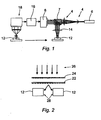
Figure 1 illustrates a comparative example of a 3d projection lithography system; -
Figure 2 illustrates a vertical patterning arrangement; -
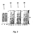
Figure 3 illustrates a tilted line in space including and idealised phase CGH for a tilted line and simulated image intensities at three mask-substrate separations. -
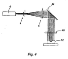
Figure 4 illustrates proximity lithography with a holographic mask. - Embodiments of the present invention seek to address the need for achieving the projection of focused fine-pitch patterns over defined 3d surfaces and vertical or sloping side walls by a single exposure at the sub-micron scale. Features may include:
- 1. Projection of 3d surface-focused images using either coherent illumination or light with limited spatial coherence such that the pattern remains sharply in focus over the extent of the surface. Partial coherence may be used to reduce speckle.
- 2. Extended DOF lines using fresnel CGH patterns by using projection or proximity exposure. The use of a (possibly large) proximity gap between substrate and mask alters the DOF properties, but does not limit the resolvable line width.
- 3. With reference to
Figure 2 , the combination of a phase grating 22 with aCGH 24 illuminated withradiation 26 to project focused patterns on vertical or slopingside walls 28 of thesubstrate 12, making possible much larger depth of field. - 3a. The use of curved gratings to project patterns on the inside of cylindrical or other curved holes.
- 4. Reduce demands of alignment accuracy in the z-direction (as orientated along the optical axis) by the use of patterns having extended DOF. This has ramifications for both planar and 3d surfaces.
- 4a. In the planar substrate scenario there is potential to reduce the extremely demanding alignment accuracy and tolerance demands of process control at sub-micron feature sizes.
- 4b. For 3d substrates this capability eases the burden of a) alignment precision in z-direction b) removal of off-axis tilt errors c) the need for precise measurement of the surface topography d) the need to deposit entirely uniform layers of photoresist.
- 5. A system whereby the DOF has been tailored for a given 3d substrate such that the aforementioned burdens described in 4 above are balanced with the image requirements (minimum line width, line profile and coherence set up of illumination).
- 6. Methods for the deposition of very thin layers of photoresist over grossly non-planar surfaces.
- 7. DH (Digital Holography) related inspection techniques such as use of DH recorded holograms of the substrate may be combined with representations of the desired image pattern to derive a CGH unique to each respective object.
- 8. A scanning embodiment of 7 such that the object is scanned (for example in 1d), a CGH is computed in real-time and exposure of the pattern immediately follows in synchronicity.
- 9. Methods for computing the CGH for 3d patterning using both proximity and projection exposure arrangements.
- 9a. Use of width and length-controlled line segments with modified implementations for projection by phase or amplitude SLMs.
- 9b. Direct inverse propagation between the pattern superimposed on the 3d surface and the (planar) CGH. This results in a direct transform between the two surfaces and as such enables restrictions to the CGH encoding (e.g. a phase only modulation) and reinforcement of the object intensity distribution to be applied directly in a series of iteration cycles. This process may be applied as a series of planar slices or tiled segments from which the 3d object pattern is represented, but they rely on a 'rippling' of the constraints between each slice or segment before returning to the CGH plane. Two possible aspects to this approach are: Firstly, the application of well-known optical propagation formulae such as the Rayleigh-Sommerfeld diffraction formula to non-planar surfaces. This kind of generalised approach is computationally intensive but is free from planar restrictions of faster methods such as those based on Fresnel Diffraction Formula (FDF) and Angular Spectrum (AS) representations. Secondly, the addition of iterative techniques to apply restriction to the CGH and object surfaces.
- These are described further below.
- 1. With reference to
Figure 1 , theoptical system arrangement 2 utilises a UV beam collimated byillumination optics 4 from aradiation source 6 such as a suitably prepared UV laser arc lamp source to illuminate, via anoptical element 7, the surface of the wave front control means 8 that is in this example a wave front modulator such as an SLM or CGH photomask which performs wave front modulation. The resulting wave travels via a projection means 10 to thesubstrate 12, possibly passing through aprojection lens assembly 14, otherwise by free space propagation. TheSLM 8 is programmed, by a configuration means 16, with a modulation pattern that is determined by thesubstrate 12 geometry or topography and desired pattern. The substrate geometry or topography is provided by DH surface profilometery performed by aDH microscope 18, which provides geometrical or topographical input to theCGH calculation routines 16. The topography may be measured with the bare substrate before resist is coated or after resist coating, when the substrate comprises resist. An alternative arrangement is shown inFigure 2 for vertical or sloping surface patterning whereby a grating 22 has been superimposed onto theCGH pattern 24 to generate +1 and -1 orders. TheSLM 8 can take the form of a Liquid Crystal device such as Liquid Crystal on Silicon (LCoS) or a micromirror array. These devices offer pixel dimensions in the region of 10-20 µm. If smaller pixels are required the CGH reticle can be fabricated using a fixed pattern using e.g., chrome on glass. - 2. When line segments are encoded by the CGH as cylindrical lines, an interesting property of the CGH representation is the relationship between DOF and imaging distance. Since the alias-limited CGH size is dependent on the image distance it is possible to maintain a constant line width for a fixed pixel size. The DOF however may increase as the imaging distance increases, the trade off being a reduction in the gradient of the intensity profile.
With reference toFigure 3 , an idealised phase CGH for a tiltedline 30, results in simulated image intensities at three mask-substrate separations, 32, 34 and 36.
This technique offers increased DOF for certain configurations. For example optically fast lithographic systems have a notoriously small DOF which makes z-axis alignment difficult. The larger DOF afforded by the methods described herein enables a relaxation of z-alignment precision and permits the use of less flat substrates.
A cylinder whose cross section is an ellipse, parabola, or hyperbola is called an elliptic cylinder, parabolic cylinder, or hyperbolic cylinder. Such cylindrical shapes may also be used for the cylindrical lines. - 3. This is based on a previous method by Philips but addresses the key limitation regarding depth of field using combined CGH / grating mask. The CGH maintains focusing of the image in the same way as for the coplanar arrangements described above but now in the vertical plane. The CGH can also remove distortions incurred due to the off-axis incidence of the +1 and -1 orders and hence recovering the original pattern.
- 4. This is about ramification of engineering the DOF of the system to reduce the demands of physical alignment and CGH design. There would still be a need for accurate x-y alignment (as with planar lithography). it would be extremely advantageous if the z offset accuracy could be relaxed and if the image could still projected in the presence of tilt errors. We have effectively capitalised on this property for larger 3d lithography where the local line DOF is quite large. Furthermore, the CGH currently assumes an exact substrate geometry, whereas in fact the actual substrate does not have ideal dimensions but rather is subject to manufacturing tolerances. Although it is possible to design a unique CGH for each object (as described in 1) the preferred arrangement would be a nominal CGH that whose image has sufficient latitude to accommodate substrate variations. DH scanning would then be used to locate larger variations in substrate shape and only adapt the CGH if they are within acceptable tolerances. This is a similar argument with respect to photoresist uniformity where small variations in thickness are compensated by having wider region over z in which the intensity is above a threshold value.
- Embodiments of the present invention develop the existing concept of holographic photolithography originally developed for 100 µm-scale devices to sub-µm resolution and address the following aspects of the invention: computation of CGH exposure masks; development of process enhancements to address substrate preparation and exposure requirements; and modelling, design and characterisation of the optical exposure system. The outcome can be assessed by examining the balance achieved between the computation burden, speed and cost of the approach versus the process latitude, quality and yield.
- Two fundamental optical configurations are possible: projection exposure using reduction lenses and proximity exposure. The image quality of these systems can be assessed for both spatially coherent (laser) and partially spatially coherent (UV lamp) illumination and with further modification of the system and mask configuration (as described), high density interconnect structures on vertical side-walls can be created.
- The purpose of the CGH exposure mask is to control the pattern intensity profile in 3d. To this end, the critical control parameters for successful fabrication are feature shape and intensity control in x, y and z.
- For objects comprising one or more tilted planes or tiles the Angular Spectrum (AS) method [Tommasi] and the generalised Rayleigh-Sommerfeld (RS) formulation [Born] for light propagation can be employed in order to encode the pattern into the CGH. These approaches do not require approximations to the scalar wave equation. Rapid numerical calculation strategies (see for example [Shen]) can be applied. For objects comprising geometrical shapes representable by mathematical functions, the CGH can be defined by a direct optical transform of the input pattern [Rosen]. For object surfaces reducible to neither tiles nor simple shapes the RS method may be used in its most general form. For a given 3d object surface pattern U(ξ,η,z), as determined by the DHM R-1000 surface recording, the complex light distribution in the CGH plane H(x,y,z0) can be computed by the following discrete summation:

where r is the length of the vector traced between each object point (ξ,η.z) and the current CGH pixel location (x.y.z0) and k is the wave constant. - Where necessary iterative techniques can be used in order to restrict the solution to practical mask coding schemes. Various error reduction methods based on iteration may be suitable such as those applied extensively for adaptive optics [Fineup], beam forming [Eismann] and optical tweezers [Sinclair]. In such cases a minimum error is specified to determine successful image generation or recovery. For lithography only very small errors can be tolerated in the final exposure image in a similar vein to holographic data storage technology [Sanford] but are even more restrictive in the present application. Iteration may be employed to operate directly between the non-planar object and CGH to achieve optimal signal to noise performance.
- In addition to these somewhat general approaches the Line Segment (LS) is also applicable for the projection of 3d lines at or below the micron scale. As a consequence of the simplified representations of line patterns used in this method it is difficult to maintain control of line intensity for large depth variations. It is also challenging to achieve registration of fine pitch lines since the method is most amenable to isolated features. Both of these obstacles are addressed by the AS and RS methods. However evidence suggests (
Fig 3 ) that is scope to exploit the unusual image properties of 3d LS CGHs (in particular the inherent high signal to noise ratio of isolated features) which make them particularly suitable for lithographic patterning. Since the LS method is based on the Fresnel approximation care is need to restrict errors that manifest in projected 3d lines as dimensions reduce below the µm scale. - These algorithms when embodied in custom computer hardware enable the computation of CGH patterns on a time scale consummate with real-time non-planar surface writing when a maskless system is employed. These techniques permit real-time time systems which are limited by exposure demands rather than computational load.
- Vertical imaging using a diffraction grating to deflect the mask pattern [Nellissen] suffers from limited focal range due to diffractive line broadening. By the use of a CGH mask combined with an optimised phase grating sloping or vertical focused images are created that are suitable for patterning sloping side walls or vertical side walls that are arranged orthogonal to the CGH plane. By this arrangement distortions typically incurred by projection to the vertical plane are removed by the CGH. Optimised CG H designs can be fabricated as amplitude and phase modulation masks suitable for projection and proximity exposure. By extrapolation of the criterion that the resolution of line segments is approximately equal to the pixel pitch [Maiden] this approach enables the creation of sub-micron features on the substrate. The fabrication of multilevel phase masks, greyscale amplitude and combined phase/amplitude structures offer the possibility of increased image fidelity. Pixelation is especially problematic at extremely close proximity and vector mask representations can be developed to address this.
- For the projection case (e.g.,
Fig. 1 ) we may use an image reduction factor in the region of 10. This enables the use of comparatively low space-bandwidth SLMs or CGH masks written by laser or e-beam pattern generators. For the proximity case (e.g.Fig. 4 ) in-house masks with a minimum feature sizes of -0.5 µm enable the creation of high resolution 3d patterns suitable for applications such as MEMS and 3d chip stacking applications. As the CGH pixel dimension approaches that of the wavelength of illumination it becomes necessary to consider both the approximation inherent within the scalar wave representation [Born] and to draw upon the multitude of possible Resolution Enhancement Techniques (RET) devised originally by the semiconductor fabrication industry for planar imaging [Wong]. - A CGH is normally used to store the interference pattern representing objects located at different positions in space. In an embodiment of the present invention the objects are circuit-like features (lines, pads, buses) that are brought to sharp focus at predetermined locations on a 3d surface. They are defined here as idealised objects in a computer, although a physical replica of the object could be used to optically record the interference pattern in a suitable medium (more on this below). In the computer a numerical propagation routine may be used to find the interference pattern. The numerical routine used depends on properties of the physical propagation medium, but this approach generally involves the scalar Helmholz equation with corresponding assumptions of a linear, isotropic and homogeneous medium.
- The conventional means for recovering the object image pattern involves illumination with a reference beam which may be on-axis (i.e., normal to the surface of the CGH) or at some angle to the surface of the CGH. This causes an intensity pattern to appear at some distance from the CGH that is matched to the intended object surface. The quality of the reconstruction depends on several factors such as the size and granularity (pixel dimension) of the CGH (i.e. the space-bandwidth) and properties of the illumination used. The critical point is that, provided the reference beam is an exact conjugate replica of reference used in the numerical computation of the CGH, then the object intensity pattern appears in free space with 1:1 scale.
- In order to reproduce a scaled-down version of the object intensity pattern, a lens (or a system of lenses) can be placed some distance from the CGH such that the intensity pattern is transmitted through the lens (or lens system) and appears on the opposite side reduced in size by some factor, n. n typically takes a value between 4 and 10 in photolithography applications.
- When this procedure is carried out without any alteration to the CGH, a distorted scaled copy of the intensity pattern will appear due to the basic properties of refractive imaging. This commonly manifests '3d perspective' errors in the form of scaling of both the transverse (x,y) dimensions and axial dimensions, making the object appear distorted. The degree of distortion is related to the geometrical arrangement between the lens and the object pattern created by the CGH.
- The approach taken by embodiments of the present invention is based on the realisation that pre-distortions may be applied to the object stored in the computer such that its CGH produces an appropriately distorted 3d image. When the modified image is passed through a lens (system), the corrected pattern appears. This approach affords great freedom to accommodate different system configurations (different arrangements of radiation source, wave front modulator, projection system and substrate) since the object is stored as a CGH and can thus is readily modified.
- The CGH is adjusted such that the axial scaling of features of the object pattern are adjusted according to the projection arrangement. Transverse (x-y) features are scaled by a factor according to their location along the optical axis. The overall object is also scaled along the axial direction by a different factor. This adjustment takes the general form of a spatial transform which is a function of the system parameters (lens system properties such as focal lengths, numerical aperture, proximity between CGH image and lens, and reduction factor n) and the object pattern location.
- An equivalent optically generated hologram may be recorded by a. constructing a correctly scaled object (made smaller by the factor n), b. placing it in front of the projection lens (system), c. illuminating said object with the desired pattern in a suitable fashion to create an object wave front which passes though the lens (system) (this step would itself be difficult without some kind of 3d imaging system to create the pattern on the object surface), d. transforming said wave front into an interference intensity pattern using a second reference wave front and e. recording the intensity pattern in a suitable photosensitive medium. This method would be very cumbersome and inconvenient to handle many different object shapes and patterns.
- These adjustments may then be appropriately encoded into the CGH and constrained in the same manner as the non-projected case. To do this a set of parameters pertaining to limitations imposed by the wave front modulator are applied to the CGH solution. Parameters may include modulator pixel size, modulation mode (phase or amplitude) and number of quantised levels. A non-distorted image will result when the proper adjustments have been made to the object and 'encoded' by the CGH for correct display by the wave front modulator.
- With reference to
Figure 4 a conventional fixedCGH mask 40 could also be used in place of a wave front modulator using essentially the same procedure, as indicated by the elements laser /lamp 6,illumination optics 4 andsubstrate 12 in common withFigure 1 and with amirror 42 replacing theoptical element 7. - A digital holographic (DH) microscope (8 in
Figure 1 ) may be used to determine the precise substrate shape prior to imaging. The measured shape may be used to generate the optimised CGH for that substrate, which can then be projected via an SLM. - Features encoded into the CGH can be added in order to assist with mask-to-substrate alignment. These can for example take the form of Fresnel zone plates that locate onto fiducial marks on the substrate and can be designed for illumination with red light in order that the photoresist is not affected during the alignment procedure. An expanded laser beam can be used to illuminate the CGH which gives highly coherent illumination, but in order to get a sufficiently flat intensity distribution the central portion of the beam can be used, thus wasting most of the beam power and leading to longer exposure times. Diffractive and refractive beam reshapers may be employed to generate a near top-hat intensity profile and hence improve efficiency. Diffractive reshapers are easier to integrate within the optical system but exhibit particular effects on the resulting image due to the phase distortions that they induce.
- Deep sub-micron planar lithography makes great use of partial coherence control and off-axis illumination to enhance process latitude [Wong]. There are considerable advances to be made by applying these to the patterning of 3d substrates, but attempts to do this are not known. Reduced spatial coherence introduces a controllable speckle reduction, permitting a degree of spatial localisation of the CGH. This affords a corresponding localisation in the calculation of the CGH hence a reduction of the memory (RAM) needed for computation. A wavelength-filtered mercury arc lamp source (standard mask aligner light source) together with bespoke optics provides a suitable light source for this purpose.
- Projecting holographic images using coherent UV illumination and both DMD and LCoS devices, including the use of scanning techniques [Clube] is distinct from traditional incoherent visible light applications in that the device response and damage threshold tolerance is different in the coherent UV regime, causing degradation of the maximal birefringence of the device at high power densities [Remenyi]. Maskless holographic lithography, particularly in projection configuration, creates an efficient utilisation of the relatively coarse pixels arrays found in typical DMD (~13.5 µm) and LCD (-8 µm) arrays and hence enables sub-micron patterning by step and repeat or multiple exposure procedures.
- To date 3d lithography research has concentrated on feature sizes of the order of 10 µm using photoresist with a thickness of 3-10 µm. The definition of sub-micron features may require a corresponding reduction in photoresist thickness. This precludes the use of standard electrophoretic photoresist formulations, since these have a minimum thickness of -3 µm. However, the thickness can be reduced into the sub-micron realm by suitable process modification and addition of extra components to the negative- and positive-acting formulations. These components are known to be highly volatile, so process control is an important factor in achieving reproducible results. The resist thickness must remain near-uniform even after the preliminary soft-bake step, so careful optimisation is needed to control the process.
- The patterning of 60 µm-pitch tracks over 300 µm steps has been demonstrated using spray-on resist [Fischer], with the authors noting that the minimum line width was governed by diffractive line broadening which can be directly alleviated by embodiments of the present invention.
- The substrates may be manufactured by anisotropic etching of suitable orientated silicon wafers to generate sloping and vertical surfaces. This is the standard method used in MEMS and MOEMS applications. More complex substrate shapes may be created using machinable glass-ceramics.
- Embodiments of the present invention address the difficulty of fabricating MEMS devices and chip to chip packaging.
- By way of example, TSVs (Through-Silicon Vias) can be created on anisotropically-etched silicon wafer. With a pitch of 2 µm a single 2x2 mm square hole could potentially carry 2,600 tracks. This is equivalent to a vertical routing density of 650 vias/mm2. A 10 µm TSV pitch would be required to achieve the same routing density, but in this case electroplating considerations mean that the wafer must be thinned in order to keep the aspect ratio of the hole low. At this pitch there would be no room for active circuitry, as is obviously also the case with a single large hole. Embodiments of the present invention may work with non-thinned wafers and also eliminate the need for a custom laser drilling step, since the large holes are made using a standard wet chemistry etching process.
- TSVs carry a single electrical connection. However the patterning of multiple connections down a single vertical hole can be achieved by combining a CGH with a diffraction grating as described in accordance with an embodiment of the present invention. For example, a 1 mm diameter vertical-walled hole and a track pitch of 2 µm equates to a track density of -400 tracks/ mm2. The same scheme may be applicable for patterning tracks in rectangular slots or on the straight edges of diced chips. Once again, this routing density is achieved in full-thickness wafers. Using the same CGH/diffraction grating combination the patterning of non-vertical features onto vertical side walls is equally possible. This could include, for instance, the patterning of a helical micro inductor.
- Many microsystems contain curved surfaces over which it is required to pattern electrical or diffractive structures. For instance, fly's eye type cameras and sensors, microfluidic electrode arrays and gratings on curved lenses.
- Passive elements such as capacitors and inductors can now be created as 3d volume elements instead of planar components. For example a MEMS device etched to create a hole some 400 µm in diameter could be patterned according to embodiments of the present invention to create a spiral descending track into the hole giving a solenoidal inductor.
- In addition capacitor plates can be created according to embodiments of the present invention on sloping surfaces where the area of overlap between them may be affected by vibration or thermal expansion or other physical generating effects and so produce an electrical method of measuring the physical change.
- Further modifications and improvements may be added without departing from the scope of the invention described in the claims.
-
- S. Bühling, F. Wyrowski, E-B. Kley, A. J. M. Nellisen, L. Wang and M. Dirkzwager, 'Resolution enhanced proximity printing by phase and amplitude modulating masks', J. Micromech. Microeng. 11 603-611 (2001).
- L. G. Neto, P. S. P. Cardona, G. A. Cirino, R. D. Mansano and P. Verdonck, 'Design, fabrication and characterization of a full complex-amplitude modulation diffractive optical element' SPIE J. Micro/Nanolithography, MEMS and ).
- Y. Borodovsky, W-H. Cheng, R. Schenker and V. Singh, 'Pixelated phase masks as novel lithography RET', Proc. SPIE 6924 69240E (2008).
- T. Nellissen, M. Botermans, M. Burghoorn, J. van Delft, E, van Grunsven, J. Scheer and M. de Samber, 'A novel photolithographic method for realizing 3-d interconnection patterns on electronic modules', 14th IMAPS European Microelectronics and Packaging Conference & Exhibition, Prague, Czech Republic (2004).
- C. Frère, D. Leseberg and O. Bryngdahl, 'Computer-generated holograms of three-dimensional objects composed of line segments', J. Opt. Soc. Am. 3(5) 726-730 (1986).
- K. Fischer and R. Süss, 'Spray coating - a solution for resist film deposition across severe topography', IEEE EMT Symposium 338-341 (2004).
- T. Tomassi and B Bianco, 'Computer-generated holograms of tilted planes by a spatial frequency approach', J. Opt. Soc. Am. A 10(2), 200-305 (1993).
- M. Born and E. Wolf Principles of Optics, 6th Ed., Pergamon Press, Oxford (1980).
- J.R. Fienup, 'Phase retrieval algorithms: a comparison', Appl. Opt. 21(15), 2758-2769 (1982).
- M.T. Eismann, A.M. Tai and J.N. Cederquist, 'Iterative design of a holographic beamformer', Appl. Opt. 28(13), 2641-2650 (1989).
- G. Sinclair, J. Leach, P. Jordan, G. Gibson, E. Yao, Z. J. Laczik, M. J. Padgett and J. Courtail, 'Interactive application in holographic optical tweezers of a multiple-plane Gerchberg-Saxton algorithm for three-dimensional light shaping', Opt. Express 12(8), 1665-1670 (2004).
- J. L. Sanford, P. F. Greier, K. H. Yang, M/ Lu, R. S. Olyha, C. Narayan, P. Alt and R. Melcher, 'A one-megapixel spatial light system for holographic data storage', IBM J. R&D 42 (3-4) 411-426 (1998).
- F. Shen and A. Wang, 'Fast-Fourier-transform based numerical integration method for the Rayleigh-Sommerfeld diffraction formula', Appl. Opt. 45(6), 1102-1110 (2006).
- F. Clube, S. Gray, D. Struchen, S. Malfoy, Y. Darbellay, N. Magnon, B. Le Gratiet and J-C. Tisserand, 'Large-field, high-resolution photolithography', Proc. SPIE 3099, 36-45 (1997).
- A. K-K. Wong Resolution Enhancement Techniques in optical lithography, SPIE press, WA (2001).
- A. Maiden, R. P. McWilliam, A. Purvis, S. Johnson, G. L. Williams, N. L. Seed and P. A. Ivey, "Non-planar photolithography with computer generated holograms," Optics Letters 30(11) 1300-1302 (2005).
- J. Rem6nyi, P. Virhegyi, L. Domján, P. Koppa and E. Lõrincz "Amplitude, phase, and hybrid ternary modulation modes of a twisted-nematic liquid-crystal display at -400 nm", Appl. Opt. 42(17), 3428-3434 (2003).
- J. Rosen, 'Computer-generated holograms of images reconstructed on curved surfaces', Appl. Opt. 38(29), 6136-6140 (1999).
- T. Poon, B. Lee, H. Yoshikawa, and W. Osten, "Digital holography and 3D imaging: introduction to the feature issue," Appl. Opt. 47(19), (2008).
- A. Maiden, R. P. McWilliam, A. Purvis, S. Johnson, G. L. Williams, N. L. Seed and P. A. Ivey, "Non-planar photolithography with computer generated holograms," Optics Letters 30(11) 1300-1302 (2005).
Claims (14)
- An exposure apparatus for vertical or sloping surface patterning of a substrate whereby the exposure apparatus comprises a phase grating (22) and a computer generated hologram (CGH) (24) illuminated with radiation (26) and configured to project focused patterns on vertical or sloping side walls (28) of the substrate (12).
- The exposure apparatus of claim 1, wherein the computer generated hologram (CGH) (24) is configured to maintain focusing of the image in a vertical plane.
- The exposure apparatus of claim 1 or claim 2, wherein the grating (22) is configured to be superimposed onto a computer generated hologram (CGH) pattern to generate +1 and -1 orders.
- The exposure apparatus of claim 3, wherein the computer generated hologram (CGH) (24) is configured remove distortions incurred due to the off-axis incidence of the +1 and -1 orders.
- The exposure apparatus of any previous claim, wherein the radiation is coherent or has limited spatial coherence.
- The exposure apparatus of any previous claim, wherein the computer generated hologram (CGH) (24) comprises Fresnel patterns.
- The exposure apparatus of any previous claim, wherein the phase grating is curved to project patterns on the inside of cylindrical or other curved holes.
- The exposure apparatus of any previous claim, wherein line segments of the patterns are encoded by the computer generated hologram (CGH) (24) as cylindrical lines.
- The exposure apparatus of any previous claim, for projecting radiation corresponding to a pattern onto the substrate, wherein:- the computer generated hologram (CGH) (24) is configured to alter a wave front of the radiation;- the apparatus further comprises configuration means (16) for configuring the computer generated hologram (CGH) (24) based on the pattern and a topography of the substrate; and- the phase grating is arranged with the computer generated hologram (CGH) (24) to transform a focal plane of the altered wave front for projection on to the vertical or sloping side walls (28) of the substrate (12).
- The exposure apparatus of claim 9, wherein the configuration means (16) is operable to configure the computer generated hologram (CGH) (24) by calculating inverse propagation between non-planar topography of the substrate and the computer generated hologram (CGH) (24).
- The exposure apparatus of claim 9 or claim 10, further comprising a substrate profiling means for determining the topography of the substrate.
- The exposure apparatus of claim 11, wherein the substrate profiling means comprises a digital holography inspection apparatus.
- A method of patterning sloping side walls, or vertical side walls, the method comprising using a computer generated hologram (CGH) mask combined with a phase grating to create sloping or vertical focused images that are suitable for patterning the sloping side walls, or the vertical side walls that are arranged orthogonal to the computer generated hologram (CGH) mask plane.
- The method of claim 13, comprising projecting radiation corresponding to a pattern onto a substrate, the method further comprising the steps:- altering a wave front of the radiation;- configuring the altering based on the pattern and a topography of the substrate; and- projecting the altered wave front onto a substrate using the phase grating to transform the focal plane of the altered wave front for projection on to a vertical or sloping side wall of the substrate.
Applications Claiming Priority (2)
| Application Number | Priority Date | Filing Date | Title |
|---|---|---|---|
| GBGB0813907.3A GB0813907D0 (en) | 2008-07-30 | 2008-07-30 | Sub-micron 3d holographic lithpgraphy |
| PCT/GB2009/050945 WO2010013052A2 (en) | 2008-07-30 | 2009-07-30 | Exposure apparatus and methods |
Publications (2)
| Publication Number | Publication Date |
|---|---|
| EP2321702A2 EP2321702A2 (en) | 2011-05-18 |
| EP2321702B1 true EP2321702B1 (en) | 2013-07-17 |
Family
ID=39747160
Family Applications (1)
| Application Number | Title | Priority Date | Filing Date |
|---|---|---|---|
| EP09785419.4A Not-in-force EP2321702B1 (en) | 2008-07-30 | 2009-07-30 | Exposure apparatus and methods |
Country Status (4)
| Country | Link |
|---|---|
| US (2) | US9046874B2 (en) |
| EP (1) | EP2321702B1 (en) |
| GB (2) | GB0813907D0 (en) |
| WO (1) | WO2010013052A2 (en) |
Families Citing this family (18)
| Publication number | Priority date | Publication date | Assignee | Title |
|---|---|---|---|---|
| US9025136B2 (en) * | 2008-09-23 | 2015-05-05 | Applied Materials, Inc. | System and method for manufacturing three dimensional integrated circuits |
| WO2010101671A1 (en) | 2009-01-16 | 2010-09-10 | New York University | Automated real-time particle characterization and three-dimensional velocimetry with holographic video microscopy |
| EP2791660A1 (en) * | 2011-12-12 | 2014-10-22 | Visys NV | A system and a method for individually inspecting objects in a stream of products and a sorting apparatus comprising such system |
| US8793108B2 (en) * | 2012-03-29 | 2014-07-29 | Siemens Aktiengesellschaft | Three-dimensional model determination from two-dimensional sketch with two-dimensional refinement |
| US20140030895A1 (en) * | 2012-07-30 | 2014-01-30 | University Of Utah Research Foundation | Methods and system for generating a three-dimensional holographic mask |
| US9476764B2 (en) | 2013-09-10 | 2016-10-25 | Taiwan Semiconductor Manufacturing Co., Ltd. | Wavefront adjustment in extreme ultra-violet (EUV) lithography |
| US9405204B2 (en) | 2013-09-18 | 2016-08-02 | Taiwan Semiconductor Manufacturing Co., Ltd. | Method of overlay in extreme ultra-violet (EUV) lithography |
| US9034665B2 (en) * | 2013-10-11 | 2015-05-19 | Taiwan Semiconductor Manufacturing Co., Ltd. | Tool configuration and method for extreme ultra-violet (EUV) patterning with a deformable reflective surface |
| WO2015175046A2 (en) | 2014-02-12 | 2015-11-19 | New York University | Y fast feature identificaiton for holographic tracking and characterization of colloidal particles |
| ES2913524T3 (en) | 2014-11-12 | 2022-06-02 | Univ New York | Colloidal fingerprinting for soft materials using total holographic characterization |
| JP6929560B2 (en) | 2015-09-18 | 2021-09-01 | ニュー・ヨーク・ユニヴァーシティー | Holographic detection and characterization of large impurity particles in precision slurry |
| JP7130242B2 (en) | 2016-02-08 | 2022-09-05 | ニュー・ヨーク・ユニヴァーシティー | Holographic characterization of protein aggregates |
| EP3358321A1 (en) * | 2017-02-03 | 2018-08-08 | Wooptix S.L. | Method and optical system for acquiring the tomographical distribution of wave fronts of electromagnetic fields |
| US11340555B2 (en) * | 2019-08-22 | 2022-05-24 | Himax Display, Inc. | Adjustably multifocal 3D holographic display system |
| CN112468799B (en) * | 2019-09-06 | 2022-06-17 | 立景光电股份有限公司 | Stereoscopic holographic display system |
| US11543338B2 (en) | 2019-10-25 | 2023-01-03 | New York University | Holographic characterization of irregular particles |
| US11378915B2 (en) * | 2019-12-12 | 2022-07-05 | Intel Corporation | Real time holography using learned error feedback |
| US11948302B2 (en) | 2020-03-09 | 2024-04-02 | New York University | Automated holographic video microscopy assay |
Family Cites Families (5)
| Publication number | Priority date | Publication date | Assignee | Title |
|---|---|---|---|---|
| US6304316B1 (en) | 1998-10-22 | 2001-10-16 | Anvik Corporation | Microlithography system for high-resolution large-area patterning on curved surfaces |
| US7095484B1 (en) * | 2001-06-27 | 2006-08-22 | University Of South Florida | Method and apparatus for maskless photolithography |
| WO2006021818A1 (en) | 2004-08-24 | 2006-03-02 | University Of Durham | Holographic lithography |
| EP1910996A1 (en) * | 2005-02-23 | 2008-04-16 | Lyncee Tec S.A. | Wave front sensing method and apparatus |
| ITRM20050120A1 (en) * | 2005-03-16 | 2006-09-17 | Consiglio Nazionale Ricerche | HOLOGRAPHIC METHOD IN NUMERICAL RECONSTRUCTION TO OBTAIN A PICTURE OF A THREE-DIMENSIONAL OBJECT IN WHICH THERE ARE ALSO POINTS OUTSIDE THE DEPTH OF FIELD, AND THE HOLOGRAPHIC APPARATUS USING THIS METHOD. |
-
2008
- 2008-07-30 GB GBGB0813907.3A patent/GB0813907D0/en not_active Ceased
-
2009
- 2009-07-30 EP EP09785419.4A patent/EP2321702B1/en not_active Not-in-force
- 2009-07-30 WO PCT/GB2009/050945 patent/WO2010013052A2/en active Application Filing
- 2009-07-30 US US13/056,023 patent/US9046874B2/en not_active Expired - Fee Related
-
2010
- 2010-03-15 GB GBGB1004247.1A patent/GB201004247D0/en not_active Ceased
-
2011
- 2011-03-15 US US13/578,313 patent/US20130120813A1/en not_active Abandoned
Non-Patent Citations (1)
| Title |
|---|
| DE SAMBER M ET AL: "Through wafer interconnection technologies for advanced electronic devices", ELECTRONICS PACKAGING TECHNOLOGY CONFERENCE, 2004. EPTC 2004. PROCEEDI NGS OF 6TH SINGAPORE 8-10 DEC. 2004, PISCATAWAY, NJ, USA,IEEE, US, 8 December 2004 (2004-12-08), pages 1 - 6, XP010771589, ISBN: 978-0-7803-8821-5, DOI: 10.1109/EPTC.2004.1396566 * |
Also Published As
| Publication number | Publication date |
|---|---|
| US20130120813A1 (en) | 2013-05-16 |
| WO2010013052A2 (en) | 2010-02-04 |
| US9046874B2 (en) | 2015-06-02 |
| GB0813907D0 (en) | 2008-09-03 |
| GB201004247D0 (en) | 2010-04-28 |
| WO2010013052A3 (en) | 2010-04-01 |
| EP2321702A2 (en) | 2011-05-18 |
| US20110292363A1 (en) | 2011-12-01 |
Similar Documents
| Publication | Publication Date | Title |
|---|---|---|
| EP2321702B1 (en) | Exposure apparatus and methods | |
| US6233044B1 (en) | Methods and apparatus for integrating optical and interferometric lithography to produce complex patterns | |
| US6657208B2 (en) | Method of forming optical images, mask for use in this method, method of manufacturing a device using this method, and apparatus for carrying out this method | |
| US8524443B2 (en) | Method and apparatus for printing a periodic pattern with a large depth of focus | |
| US9036133B2 (en) | Lithographic fabrication of general periodic structures by exposing a photosensitive layer to a range of lateral intensity distributions | |
| JP5048801B2 (en) | Method and apparatus for generating complex patterns by integrating optics and interference lithography | |
| KR101109369B1 (en) | Computer generated hologram, exposure apparatus and device fabrication method | |
| EP0627666B1 (en) | Apparatus and method for changing the scale of a printed pattern | |
| CN113655693B (en) | Planar and three-dimensional micro-nano processing device based on liquid crystal spatial light modulator | |
| US7978386B2 (en) | Generation of holographic diffraction patterns | |
| US7952803B2 (en) | Lithographic apparatus and device manufacturing method | |
| EP0795803A2 (en) | Method and apparatus for holographically recording an essentially periodic pattern | |
| Purvis et al. | Photolithographic patterning of bihelical tracks onto conical substrates | |
| JP6788622B2 (en) | Diffractive element design method | |
| Williams et al. | A photolithographic process for grossly nonplanar substrates | |
| Wang | Modeling, design and optimization of computer-generated holograms with binary phases | |
| Leung et al. | Using e-beam written computer-generated holograms to test deep aspheric wavefronts | |
| KR20020069878A (en) | Non contact Method and Hologram of combined binary phase | |
| Kido et al. | New phase-shifting method for high-resolution microlithography | |
| NL1036877A (en) | Diffractive optical element, lithographic apparatus and semiconductor device manufacturing method. | |
| Purvis et al. | Use policy | |
| Maiden | Lithography in three dimensions using computer-generated holograms | |
| WO2011114143A1 (en) | Improvements in or relating to holography | |
| Smith et al. | Sub-100nm, Maskless Deep-UV Zone-Plate Array Lithography | |
| Daschner | Research on producing high quality diffractive optical elements in volume at a low cost |
Legal Events
| Date | Code | Title | Description |
|---|---|---|---|
| PUAI | Public reference made under article 153(3) epc to a published international application that has entered the european phase |
Free format text: ORIGINAL CODE: 0009012 |
|
| 17P | Request for examination filed |
Effective date: 20110225 |
|
| AK | Designated contracting states |
Kind code of ref document: A2 Designated state(s): AT BE BG CH CY CZ DE DK EE ES FI FR GB GR HR HU IE IS IT LI LT LU LV MC MK MT NL NO PL PT RO SE SI SK SM TR |
|
| AX | Request for extension of the european patent |
Extension state: AL BA RS |
|
| DAX | Request for extension of the european patent (deleted) | ||
| GRAP | Despatch of communication of intention to grant a patent |
Free format text: ORIGINAL CODE: EPIDOSNIGR1 |
|
| RIN1 | Information on inventor provided before grant (corrected) |
Inventor name: TORIZ-GARCIA, JOSE, JUAN, DE JESUS Inventor name: SEED, DR NICHOLAS, LUKE Inventor name: IVEY, PETER, ANTHONY Inventor name: PURVIS, ALAN Inventor name: CURRY, RICHARD, IAN Inventor name: MCWILLIAM, RICHARD, PETER Inventor name: WILLIAMS, GAVIN, LEWIS |
|
| GRAP | Despatch of communication of intention to grant a patent |
Free format text: ORIGINAL CODE: EPIDOSNIGR1 |
|
| GRAS | Grant fee paid |
Free format text: ORIGINAL CODE: EPIDOSNIGR3 |
|
| GRAA | (expected) grant |
Free format text: ORIGINAL CODE: 0009210 |
|
| AK | Designated contracting states |
Kind code of ref document: B1 Designated state(s): AT BE BG CH CY CZ DE DK EE ES FI FR GB GR HR HU IE IS IT LI LT LU LV MC MK MT NL NO PL PT RO SE SI SK SM TR |
|
| RAP1 | Party data changed (applicant data changed or rights of an application transferred) |
Owner name: UNIVERSITY OF DURHAM Owner name: UNIVERSITY OF SHEFFIELD |
|
| REG | Reference to a national code |
Ref country code: GB Ref legal event code: FG4D |
|
| REG | Reference to a national code |
Ref country code: CH Ref legal event code: EP |
|
| REG | Reference to a national code |
Ref country code: IE Ref legal event code: FG4D |
|
| REG | Reference to a national code |
Ref country code: AT Ref legal event code: REF Ref document number: 622567 Country of ref document: AT Kind code of ref document: T Effective date: 20130815 |
|
| REG | Reference to a national code |
Ref country code: DE Ref legal event code: R096 Ref document number: 602009017271 Country of ref document: DE Effective date: 20130912 |
|
| REG | Reference to a national code |
Ref country code: AT Ref legal event code: MK05 Ref document number: 622567 Country of ref document: AT Kind code of ref document: T Effective date: 20130717 |
|
| REG | Reference to a national code |
Ref country code: NL Ref legal event code: VDEP Effective date: 20130717 |
|
| REG | Reference to a national code |
Ref country code: LT Ref legal event code: MG4D |
|
| PG25 | Lapsed in a contracting state [announced via postgrant information from national office to epo] |
Ref country code: IS Free format text: LAPSE BECAUSE OF FAILURE TO SUBMIT A TRANSLATION OF THE DESCRIPTION OR TO PAY THE FEE WITHIN THE PRESCRIBED TIME-LIMIT Effective date: 20131117 Ref country code: HR Free format text: LAPSE BECAUSE OF FAILURE TO SUBMIT A TRANSLATION OF THE DESCRIPTION OR TO PAY THE FEE WITHIN THE PRESCRIBED TIME-LIMIT Effective date: 20130717 Ref country code: BE Free format text: LAPSE BECAUSE OF FAILURE TO SUBMIT A TRANSLATION OF THE DESCRIPTION OR TO PAY THE FEE WITHIN THE PRESCRIBED TIME-LIMIT Effective date: 20130717 Ref country code: LT Free format text: LAPSE BECAUSE OF FAILURE TO SUBMIT A TRANSLATION OF THE DESCRIPTION OR TO PAY THE FEE WITHIN THE PRESCRIBED TIME-LIMIT Effective date: 20130717 Ref country code: PT Free format text: LAPSE BECAUSE OF FAILURE TO SUBMIT A TRANSLATION OF THE DESCRIPTION OR TO PAY THE FEE WITHIN THE PRESCRIBED TIME-LIMIT Effective date: 20131118 Ref country code: SE Free format text: LAPSE BECAUSE OF FAILURE TO SUBMIT A TRANSLATION OF THE DESCRIPTION OR TO PAY THE FEE WITHIN THE PRESCRIBED TIME-LIMIT Effective date: 20130717 Ref country code: NO Free format text: LAPSE BECAUSE OF FAILURE TO SUBMIT A TRANSLATION OF THE DESCRIPTION OR TO PAY THE FEE WITHIN THE PRESCRIBED TIME-LIMIT Effective date: 20131017 Ref country code: AT Free format text: LAPSE BECAUSE OF FAILURE TO SUBMIT A TRANSLATION OF THE DESCRIPTION OR TO PAY THE FEE WITHIN THE PRESCRIBED TIME-LIMIT Effective date: 20130717 Ref country code: CY Free format text: LAPSE BECAUSE OF FAILURE TO SUBMIT A TRANSLATION OF THE DESCRIPTION OR TO PAY THE FEE WITHIN THE PRESCRIBED TIME-LIMIT Effective date: 20130717 |
|
| PG25 | Lapsed in a contracting state [announced via postgrant information from national office to epo] |
Ref country code: GR Free format text: LAPSE BECAUSE OF FAILURE TO SUBMIT A TRANSLATION OF THE DESCRIPTION OR TO PAY THE FEE WITHIN THE PRESCRIBED TIME-LIMIT Effective date: 20131018 Ref country code: LV Free format text: LAPSE BECAUSE OF FAILURE TO SUBMIT A TRANSLATION OF THE DESCRIPTION OR TO PAY THE FEE WITHIN THE PRESCRIBED TIME-LIMIT Effective date: 20130717 Ref country code: ES Free format text: LAPSE BECAUSE OF FAILURE TO SUBMIT A TRANSLATION OF THE DESCRIPTION OR TO PAY THE FEE WITHIN THE PRESCRIBED TIME-LIMIT Effective date: 20131028 Ref country code: NL Free format text: LAPSE BECAUSE OF FAILURE TO SUBMIT A TRANSLATION OF THE DESCRIPTION OR TO PAY THE FEE WITHIN THE PRESCRIBED TIME-LIMIT Effective date: 20130717 Ref country code: FI Free format text: LAPSE BECAUSE OF FAILURE TO SUBMIT A TRANSLATION OF THE DESCRIPTION OR TO PAY THE FEE WITHIN THE PRESCRIBED TIME-LIMIT Effective date: 20130717 Ref country code: PL Free format text: LAPSE BECAUSE OF FAILURE TO SUBMIT A TRANSLATION OF THE DESCRIPTION OR TO PAY THE FEE WITHIN THE PRESCRIBED TIME-LIMIT Effective date: 20130717 Ref country code: SI Free format text: LAPSE BECAUSE OF FAILURE TO SUBMIT A TRANSLATION OF THE DESCRIPTION OR TO PAY THE FEE WITHIN THE PRESCRIBED TIME-LIMIT Effective date: 20130717 |
|
| REG | Reference to a national code |
Ref country code: CH Ref legal event code: NV Representative=s name: VENI GMBH, CH |
|
| REG | Reference to a national code |
Ref country code: IE Ref legal event code: MM4A |
|
| PG25 | Lapsed in a contracting state [announced via postgrant information from national office to epo] |
Ref country code: DK Free format text: LAPSE BECAUSE OF FAILURE TO SUBMIT A TRANSLATION OF THE DESCRIPTION OR TO PAY THE FEE WITHIN THE PRESCRIBED TIME-LIMIT Effective date: 20130717 Ref country code: MC Free format text: LAPSE BECAUSE OF FAILURE TO SUBMIT A TRANSLATION OF THE DESCRIPTION OR TO PAY THE FEE WITHIN THE PRESCRIBED TIME-LIMIT Effective date: 20130717 Ref country code: CZ Free format text: LAPSE BECAUSE OF FAILURE TO SUBMIT A TRANSLATION OF THE DESCRIPTION OR TO PAY THE FEE WITHIN THE PRESCRIBED TIME-LIMIT Effective date: 20130717 Ref country code: RO Free format text: LAPSE BECAUSE OF FAILURE TO SUBMIT A TRANSLATION OF THE DESCRIPTION OR TO PAY THE FEE WITHIN THE PRESCRIBED TIME-LIMIT Effective date: 20130717 Ref country code: EE Free format text: LAPSE BECAUSE OF FAILURE TO SUBMIT A TRANSLATION OF THE DESCRIPTION OR TO PAY THE FEE WITHIN THE PRESCRIBED TIME-LIMIT Effective date: 20130717 Ref country code: SK Free format text: LAPSE BECAUSE OF FAILURE TO SUBMIT A TRANSLATION OF THE DESCRIPTION OR TO PAY THE FEE WITHIN THE PRESCRIBED TIME-LIMIT Effective date: 20130717 |
|
| PLBE | No opposition filed within time limit |
Free format text: ORIGINAL CODE: 0009261 |
|
| STAA | Information on the status of an ep patent application or granted ep patent |
Free format text: STATUS: NO OPPOSITION FILED WITHIN TIME LIMIT |
|
| PG25 | Lapsed in a contracting state [announced via postgrant information from national office to epo] |
Ref country code: IT Free format text: LAPSE BECAUSE OF FAILURE TO SUBMIT A TRANSLATION OF THE DESCRIPTION OR TO PAY THE FEE WITHIN THE PRESCRIBED TIME-LIMIT Effective date: 20130717 |
|
| 26N | No opposition filed |
Effective date: 20140422 |
|
| PG25 | Lapsed in a contracting state [announced via postgrant information from national office to epo] |
Ref country code: IE Free format text: LAPSE BECAUSE OF NON-PAYMENT OF DUE FEES Effective date: 20130730 |
|
| REG | Reference to a national code |
Ref country code: DE Ref legal event code: R097 Ref document number: 602009017271 Country of ref document: DE Effective date: 20140422 |
|
| PGFP | Annual fee paid to national office [announced via postgrant information from national office to epo] |
Ref country code: CH Payment date: 20140604 Year of fee payment: 6 |
|
| PGFP | Annual fee paid to national office [announced via postgrant information from national office to epo] |
Ref country code: FR Payment date: 20140710 Year of fee payment: 6 |
|
| PG25 | Lapsed in a contracting state [announced via postgrant information from national office to epo] |
Ref country code: SM Free format text: LAPSE BECAUSE OF FAILURE TO SUBMIT A TRANSLATION OF THE DESCRIPTION OR TO PAY THE FEE WITHIN THE PRESCRIBED TIME-LIMIT Effective date: 20130717 |
|
| PG25 | Lapsed in a contracting state [announced via postgrant information from national office to epo] |
Ref country code: MT Free format text: LAPSE BECAUSE OF FAILURE TO SUBMIT A TRANSLATION OF THE DESCRIPTION OR TO PAY THE FEE WITHIN THE PRESCRIBED TIME-LIMIT Effective date: 20130717 Ref country code: TR Free format text: LAPSE BECAUSE OF FAILURE TO SUBMIT A TRANSLATION OF THE DESCRIPTION OR TO PAY THE FEE WITHIN THE PRESCRIBED TIME-LIMIT Effective date: 20130717 |
|
| PG25 | Lapsed in a contracting state [announced via postgrant information from national office to epo] |
Ref country code: MK Free format text: LAPSE BECAUSE OF FAILURE TO SUBMIT A TRANSLATION OF THE DESCRIPTION OR TO PAY THE FEE WITHIN THE PRESCRIBED TIME-LIMIT Effective date: 20130717 Ref country code: LU Free format text: LAPSE BECAUSE OF NON-PAYMENT OF DUE FEES Effective date: 20130730 Ref country code: BG Free format text: LAPSE BECAUSE OF FAILURE TO SUBMIT A TRANSLATION OF THE DESCRIPTION OR TO PAY THE FEE WITHIN THE PRESCRIBED TIME-LIMIT Effective date: 20130717 Ref country code: HU Free format text: LAPSE BECAUSE OF FAILURE TO SUBMIT A TRANSLATION OF THE DESCRIPTION OR TO PAY THE FEE WITHIN THE PRESCRIBED TIME-LIMIT; INVALID AB INITIO Effective date: 20090730 |
|
| REG | Reference to a national code |
Ref country code: CH Ref legal event code: PL |
|
| PG25 | Lapsed in a contracting state [announced via postgrant information from national office to epo] |
Ref country code: LI Free format text: LAPSE BECAUSE OF NON-PAYMENT OF DUE FEES Effective date: 20150731 Ref country code: CH Free format text: LAPSE BECAUSE OF NON-PAYMENT OF DUE FEES Effective date: 20150731 |
|
| REG | Reference to a national code |
Ref country code: FR Ref legal event code: ST Effective date: 20160331 |
|
| PG25 | Lapsed in a contracting state [announced via postgrant information from national office to epo] |
Ref country code: FR Free format text: LAPSE BECAUSE OF NON-PAYMENT OF DUE FEES Effective date: 20150731 |
|
| PGFP | Annual fee paid to national office [announced via postgrant information from national office to epo] |
Ref country code: DE Payment date: 20190718 Year of fee payment: 11 Ref country code: GB Payment date: 20190614 Year of fee payment: 11 |
|
| REG | Reference to a national code |
Ref country code: DE Ref legal event code: R119 Ref document number: 602009017271 Country of ref document: DE |
|
| GBPC | Gb: european patent ceased through non-payment of renewal fee |
Effective date: 20200730 |
|
| PG25 | Lapsed in a contracting state [announced via postgrant information from national office to epo] |
Ref country code: GB Free format text: LAPSE BECAUSE OF NON-PAYMENT OF DUE FEES Effective date: 20200730 |
|
| PG25 | Lapsed in a contracting state [announced via postgrant information from national office to epo] |
Ref country code: DE Free format text: LAPSE BECAUSE OF NON-PAYMENT OF DUE FEES Effective date: 20210202 |