EP2320477A1 - Solar cell module, solar cell, and solar cell module manufacturing method - Google Patents
Solar cell module, solar cell, and solar cell module manufacturing method Download PDFInfo
- Publication number
- EP2320477A1 EP2320477A1 EP09808140A EP09808140A EP2320477A1 EP 2320477 A1 EP2320477 A1 EP 2320477A1 EP 09808140 A EP09808140 A EP 09808140A EP 09808140 A EP09808140 A EP 09808140A EP 2320477 A1 EP2320477 A1 EP 2320477A1
- Authority
- EP
- European Patent Office
- Prior art keywords
- solar cell
- light receiving
- receiving surface
- connecting electrode
- conductivity
- Prior art date
- Legal status (The legal status is an assumption and is not a legal conclusion. Google has not performed a legal analysis and makes no representation as to the accuracy of the status listed.)
- Withdrawn
Links
Images





Classifications
-
- H—ELECTRICITY
- H10—SEMICONDUCTOR DEVICES; ELECTRIC SOLID-STATE DEVICES NOT OTHERWISE PROVIDED FOR
- H10F—INORGANIC SEMICONDUCTOR DEVICES SENSITIVE TO INFRARED RADIATION, LIGHT, ELECTROMAGNETIC RADIATION OF SHORTER WAVELENGTH OR CORPUSCULAR RADIATION
- H10F77/00—Constructional details of devices covered by this subclass
- H10F77/20—Electrodes
- H10F77/206—Electrodes for devices having potential barriers
- H10F77/211—Electrodes for devices having potential barriers for photovoltaic cells
- H10F77/219—Arrangements for electrodes of back-contact photovoltaic cells
-
- H—ELECTRICITY
- H10—SEMICONDUCTOR DEVICES; ELECTRIC SOLID-STATE DEVICES NOT OTHERWISE PROVIDED FOR
- H10F—INORGANIC SEMICONDUCTOR DEVICES SENSITIVE TO INFRARED RADIATION, LIGHT, ELECTROMAGNETIC RADIATION OF SHORTER WAVELENGTH OR CORPUSCULAR RADIATION
- H10F19/00—Integrated devices, or assemblies of multiple devices, comprising at least one photovoltaic cell covered by group H10F10/00, e.g. photovoltaic modules
- H10F19/80—Encapsulations or containers for integrated devices, or assemblies of multiple devices, having photovoltaic cells
-
- H—ELECTRICITY
- H10—SEMICONDUCTOR DEVICES; ELECTRIC SOLID-STATE DEVICES NOT OTHERWISE PROVIDED FOR
- H10F—INORGANIC SEMICONDUCTOR DEVICES SENSITIVE TO INFRARED RADIATION, LIGHT, ELECTROMAGNETIC RADIATION OF SHORTER WAVELENGTH OR CORPUSCULAR RADIATION
- H10F19/00—Integrated devices, or assemblies of multiple devices, comprising at least one photovoltaic cell covered by group H10F10/00, e.g. photovoltaic modules
- H10F19/90—Structures for connecting between photovoltaic cells, e.g. interconnections or insulating spacers
- H10F19/902—Structures for connecting between photovoltaic cells, e.g. interconnections or insulating spacers for series or parallel connection of photovoltaic cells
- H10F19/908—Structures for connecting between photovoltaic cells, e.g. interconnections or insulating spacers for series or parallel connection of photovoltaic cells for back-contact photovoltaic cells
-
- H—ELECTRICITY
- H10—SEMICONDUCTOR DEVICES; ELECTRIC SOLID-STATE DEVICES NOT OTHERWISE PROVIDED FOR
- H10F—INORGANIC SEMICONDUCTOR DEVICES SENSITIVE TO INFRARED RADIATION, LIGHT, ELECTROMAGNETIC RADIATION OF SHORTER WAVELENGTH OR CORPUSCULAR RADIATION
- H10F77/00—Constructional details of devices covered by this subclass
- H10F77/40—Optical elements or arrangements
- H10F77/42—Optical elements or arrangements directly associated or integrated with photovoltaic cells, e.g. light-reflecting means or light-concentrating means
- H10F77/488—Reflecting light-concentrating means, e.g. parabolic mirrors or concentrators using total internal reflection
-
- Y—GENERAL TAGGING OF NEW TECHNOLOGICAL DEVELOPMENTS; GENERAL TAGGING OF CROSS-SECTIONAL TECHNOLOGIES SPANNING OVER SEVERAL SECTIONS OF THE IPC; TECHNICAL SUBJECTS COVERED BY FORMER USPC CROSS-REFERENCE ART COLLECTIONS [XRACs] AND DIGESTS
- Y02—TECHNOLOGIES OR APPLICATIONS FOR MITIGATION OR ADAPTATION AGAINST CLIMATE CHANGE
- Y02E—REDUCTION OF GREENHOUSE GAS [GHG] EMISSIONS, RELATED TO ENERGY GENERATION, TRANSMISSION OR DISTRIBUTION
- Y02E10/00—Energy generation through renewable energy sources
- Y02E10/50—Photovoltaic [PV] energy
- Y02E10/52—PV systems with concentrators
Definitions
- the present invention relates to a solar cell module including back junction solar cells, a solar cell and a solar cell module manufacturing method.
- Solar cells are expected as new energy sources owing to their capability of directly converting clean and inexhaustibly-supplied sunlight into electricity.
- the output power per solar cell is several watts.
- a solar cell module is used which is capable of providing higher output power by use of a plurality of solar cells electrically connected to each other.
- a so-called back junction solar cell has been proposed in which a plurality of n-side fine-line electrodes and a plurality of p-side fine-line electrodes are alternately formed on a back surface of a semiconductor substrate for the purpose of enlarging a light receiving area (see Japanese Patent Application Publication No. 2005-11869 ) .
- the plurality of n-side fine-line electrodes are connected to an n-side connecting electrode formed on one end portion of the semiconductor substrate.
- the plurality of p-side fine-line electrodes are connected to a p-side connecting electrode formed on the opposite end portion of the semiconductor substrate.
- One solar cell and another solar cell next to the one solar cell are electrically connected in series with the n-side connecting electrode of the one solar cell and the p-side connecting electrode of the next solar cell connected to each other through a wiring member.
- the connecting electrode of the first conductivity type has a problem of poor efficiency of collecting majority carriers.
- n-side connecting electrode in a solar cell including an n-type semiconductor substrate, for example, many of holes (minority carriers) generated around the n-side connecting electrode are recombined with electrons (majority carriers) before being diffused into the p-side fine-line electrodes. As a result, the number of electrons collected by the n-side connecting electrode is reduced.
- the first conductivity side connecting electrode cannot efficiently collect carriers as described above, incident light falling on a region of the light receiving surface on an opposite side to the first conductivity side connecting electrode cannot utilized effectively.
- the present invention has been made in consideration of the above problem, and an objective thereof is to provide a solar cell module including solar cells capable of effective use of incident light, a solar cell and a solar cell module manufacturing method.
- a solar cell module is summarized as a solar cell module including one solar cell sealed between a light receiving surface protection member and a back surface protection member.
- the one solar cell includes a semiconductor substrate of a first conductivity type having a light receiving surface and a back surface provided on an opposite side to the light receiving surface; a first conductivity side connecting electrode formed on the back surface and connected to a plurality of first conductivity side fine-line electrodes; a second conductivity side connecting electrode formed on the back surface and connected to a plurality of second conductivity side fine-line electrodes; and a light reflection member placed on the light receiving surface and having a light reflecting surface facing the light receiving surface protection member.
- the light reflection member is positioned on an opposite side to the first conductivity side connecting electrode across the semiconductor substrate.
- reflection means regular reflection by a mirror surface or the like, and diffused reflection by scattered reflection or the like.
- incident light falling on a region of the light receiving surface on the opposite side to the first conductivity side connecting electrode is guided to a region other than the region on the opposite side to the first conductivity side connecting electrode.
- This structure can suppress generation of photogenerated carriers in the proximity of the first conductivity side connecting electrode, and can promote generation of photogenerated carriers in the proximity of the second conductivity side connecting electrode.
- photogenerated carriers even minority carriers having a short diffusion length, is prevented from being recombined because the distance to the second conductivity side connecting electrode is short. Therefore, incident light falling on the region on the opposite side to the first conductivity side connecting electrode can be effectively utilized.
- the first conductivity side connecting electrode may be formed on one end portion of the semiconductor substrate, and the light reflection member may reflect incident light falling on the light reflection member toward another end portion of the semiconductor substrate.
- the solar cell module may comprise another solar cell sealed between the light receiving surface protection member and the back surface protection member, wherein the other solar cell may comprise: a semiconductor substrate of a first conductivity type having a light receiving surface and a back surface provided on an opposite side to the light receiving surface; a first conductivity side connecting electrode formed on the back surface and connected to a plurality of first conductivity side fine-line electrodes; a second conductivity side connecting electrode formed on the back surface and connected to a plurality of second conductivity side fine-line electrodes; and a light reflection member placed on the light receiving surface and having a light reflecting surface facing the light receiving surface protection member, in the other solar cell, the light reflection member may be positioned on an opposite side to the first conductivity side connecting electrode across the semiconductor substrate, and the light reflection member included in the one solar cell and the light reflection member included in the other solar cell maybe formed integrally as a single unit.
- the other solar cell may comprise: a semiconductor substrate of a first conductivity type having a light receiving surface and a back surface provided on an opposite side
- the light reflecting surface may be made of any one of a metal layer and a white resin.
- the light reflection plate may include a base bonded to the light receiving surface.
- a solar cell is summarized as comprising: a semiconductor substrate of a first conductivity type having a light receiving surface and a back surface provided on an opposite side to the light receiving surface; a first conductivity side connecting electrode formed on the back surface and connected to a plurality of first conductivity side fine-line electrodes; a second conductivity side connecting electrode formed on the back surface and connected to a plurality of second conductivity side fine-line electrodes; and a light reflection member placed on the light receiving surface, and having light reflection facing the light receiving surface protection member, wherein the light reflection member is positioned on an opposite side to the first conductivity side connecting electrode across the semiconductor substrate.
- the light reflecting surface is made of any one of a metal layer and a white resin.
- the light reflection plate includes a base bonded to the light receiving surface.
- a method of manufacturing solar cell module is summarized as including one solar cell and another solar cell sealed between a light receiving surface protection member and a back surface protection member, the method comprising: a step A of forming each of the one solar cell and the other solar cell by preparing a semiconductor substrate of a first conductivity type having a back surface which is provided on an opposite side to a light receiving surface and has a first conductivity side connecting electrode and a second conductivity side connecting electrode formed thereon, with the first conductivity side connecting electrode connected to a plurality of first conductivity side fine-line electrodes, and the second conductivity side connecting electrode connected to a plurality of second conductivity side fine-line electrodes formed on the back surface, and by arranging a light reflection member on the light receiving surface of the semiconductor substrate; a step B of forming a solar cell string by electrically connecting the first conductivity side connecting electrode of the one solar cell and the second conductivity side connecting electrode of the other solar cell by use of a wiring member; and a step C of stacking
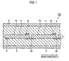
- Fig. 1 is a side view of a solar cell module 100.
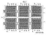
- Fig. 2 is a plan view of solar cell strings 1 when viewed from a back surface side.
- Fig. 3 is a plan view of the solar cell strings 1 when viewed from a light receiving surface side.
- the solar cell module 100 includes two solar cell strings 1, a light receiving surface protection member 2, a back surface protection member 3, a sealing member 4, a bridge wiring member 5 and a pair of output leads 6.
- the two solar cell strings 1 are sealed by the sealing member 4 between the light receiving surface protection member 2 and the back surface protection member 3.
- Each of the solar cell strings 1 includes a plurality of solar cells 10 and a plurality of wiring members 20.
- the plurality of solar cells 10 are so-called back junction solar cells each including a plurality of n-side fine-line electrodes 13n and a plurality of p-side fine-line electrodes 13p formed on a back surface of an n-type semiconductor substrate 11, as shown in Fig. 2 .
- the solar cells 10 are arrayed in an array direction H.
- the plurality of solar cells 10 are electrically connected to each other through the plurality of wiring members 20.
- Each solar cell 10 includes a light reflection member 12 placed on the light receiving surface of the n-type semiconductor substrate 11 as shown in Fig. 3 .
- the structure of the solar cell 10 will be described in details later.
- Each of the wiring members 20 electrically connects together one solar cell 10 and another solar cell 10 next to the one solar cell 10. Specifically, one end portion of the wiring member 20 is placed on an n-side connecting electrode 14n (see Fig. 4 ) of the one solar cell 10. In addition, the other end portion of the wiring member 20 is placed on a p-side connecting electrode 14p (see Fig. 4 ) of the other solar cell next to the one solar cell 10.
- a conductive material such as a thin-plate-shaped copper, for example, can be used as the wiring member 20. A surface of such a conductive material may be covered with a soft conductive material such as a lead-free solder (for example, SnAg 3.0 Cu 0.5 ).
- the light receiving surface protection member 2 protects the surface of the solar cell module 100.
- a glass, a light-transmissive plastic or the like having light-transmissive and water blocking properties can be used as the light receiving surface protection member 2.
- the back surface protection member 3 protects the back surface of the solar cell module 100.
- a resin film made of PET (Polyethylene Terephthalate) or the like, a laminate film having a structure in which a metal foil such as an A1 foil is sandwiched between resin films, or other similar films can be used as the back surface protection member 3.
- the sealing member 4 seals the two solar cell strings 1 between the light receiving surface protection member 2 and the back surface protection member 3.
- a light-transmissive resin such as an EVA, EEA, PVB, silicon, urethane, acryl, or epoxy resin can be used as the sealing member 4.
- the bridge wiring member 5 electrically connects the solar cell strings 1 to each other. Specifically, one end portion of the bridge wiring member 5 is placed on the n-side connecting electrode 14n of the solar cell 10 located at one end of one of the solar cell strings 1. In addition, the other end portion of the bridge wiring member 5 is placed on the p-side connecting electrode 14p of the solar cell 10 located at one end of the other solar cell string 1.
- the bridge wiring member 5 is made of a material similar to a material for the wiring member 20.
- the pair of output leads 6 output electric currents from the two solar cell strings 1 to the outside.
- the pair of output leads 6 are connected to the pair of solar cells 10, respectively, located at two ends of the respective two solar cell strings 1 connected together with the bridge wiring member 5.
- Each of the output leads 6 is made of a material similar to a material for the wiring member 20.
- an A1 flame can be attached to an outer periphery of the solar cell module 100 having the foregoing structure.
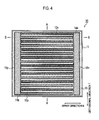
- Fig. 4 is a plan view of the solar cell 10 on the back surface side.
- Fig. 5 is an enlarged cross sectional view taken along a line A-A in Fig. 4 .
- the solar cell 10 includes an n-type semiconductor substrate 11, a plurality of n-side fine-line electrodes 13n, a plurality of p-side fine-line electrodes 13p, an n-side connecting electrode 14n, a p-side connecting electrode 14p, an n-type amorphous semiconductor layer 15n, a p-type amorphous semiconductor layer 15p, and a passivation layer 16.
- the n-type semiconductor substrate 11 has a light receiving surface for receiving light and a back surface provided on the opposite side to the light receiving surface.
- the n-type semiconductor substrate 11 according to the present embodiment is made of a semiconductor material doped with an n-type dopant.
- Materials usable as such a semiconductor material are general semiconductor materials such as crystalline semiconductor materials of single-crystal Si, polycrystalline Si and the like, and compound semiconductor materials of GaAs, InP and the like.
- the n-type semiconductor substrate 11 generates photogenerated carriers (holes and electrons) by receiving light.
- the photogenerated carriers includes the electrons as majority carriers and the holes as minority carriers.
- the plurality of n-side fine-line electrodes 13n are collecting electrodes that collect the electrons from the n-type semiconductor substrate 11.
- Each of the n-side fine-line electrodes 13n is formed along the array direction H on the back surface of the n-type semiconductor substrate 11 as shown in Fig. 4 .
- the plurality of p-side fine-line electrodes 13p are collecting electrodes that collect the holes from the n-type semiconductor substrate 11.
- the p-side fine-line electrodes 13p are formed along the n-side fine-line electrodes 13n on the back surface of the n-type semiconductor substrate 11 as shown in Fig. 4 .
- the n-side fine-line electrodes 13n and the p-side fine-line electrodes 13p are formed alternately into a form of stripes.
- each of the n-side fine-line electrodes 13n includes an n-side transparent conductive layer 13n 1 and an n-side conductive layer 13n 2 .
- the n-side conductive layer 13n 2 is formed on the n-side transparent conductive layer 13n 1 .
- the n-side transparent conductive layer 13n 1 is formed on the n-type amorphous semiconductor layer 15n.
- the n-side transparent conductive layer 13n 1 is formed of an oxide of In, Zn, Sn, Ti, W or the like.
- the n-side conductive layer 13n 2 is formed of silver, a resin conductive paste or a sintered conductive paste.
- each of the p-side fine-line electrodes 13p includes a p-side transparent conductive layer 13p 1 and a p-side conductive layer 13p 2 .
- the p-side conductive layer 13p 2 is formed on the p-side transparent conductive layer 13p 1 .
- the p-side transparent conductive layer 13p 1 is formed on the p-type amorphous semiconductor layer 15p.
- the p-side transparent conductive layer 13p 1 is formed of an oxide of In, Zn, Sn, Ti, W or the like.
- the p-side conductive layer 13p 2 is formed of silver, a resin conductive paste or a sintered conductive paste.
- the n-side connecting electrode 14n is formed along an orthogonal direction T substantially orthogonal to the array direction H, on one end portion of the n-type semiconductor substrate 11, as shown in Fig. 4 .
- the n-side connecting electrode 14n is connected to the plurality of n-side fine-line electrodes 13n.
- the n-side connecting electrode 14n is an electrode to which the wiring member 20, the bridge wiring member 5, or the output lead 6 is to be connected.
- the n-side connecting electrode 14n is a collecting electrode for collecting electrons from the n-type semiconductor substrate 11.
- the p-side connecting electrode 14p is formed along the orthogonal direction T on another end portion of the n-type semiconductor substrate 11, as shown in Fig. 4 .
- the p-side connecting electrode 14p is connected to the plurality of p-side fine-line electrodes 13p.
- the p-side connecting electrode 14p is an electrode to which the wiring member 20, the bridge wiring member 5, or the output lead 6 is to be connected.
- the p-side connecting electrode 14p is a collecting electrode for collecting holes from the n-type semiconductor substrate 11.
- the n-side connecting electrode 14n has a structure similar to the structure of the n-side fine-line electrodes 13n (see Fig. 7 ) .
- the p-side connecting electrode 14p has a structure similar to the structure of the p-side fine-line electrodes 13p, though not illustrated.
- the n-type amorphous semiconductor layer 15n is formed in a comb-like shape on the back surface of the n-type semiconductor substrate 11.
- the plurality of n-side fine-line electrodes 13n each extending in the array direction H and the n-side connecting electrode 14n extending in the orthogonal direction T are provided on the n-type amorphous semiconductor layer 15n.
- the p-type amorphous semiconductor layer 15p is formed in a comb-like shape on the back surface of the n-type semiconductor substrate 11.
- the plurality of p-side fine-line electrodes 13p each extending along the array direction H and the p-side connecting electrode 14p extending along the orthogonal direction T are provided on the p-type amorphous semiconductor layer 15p.
- the n-type amorphous semiconductor layer 15n and the p-type amorphous semiconductor layer 15p are formed on the passivation layer 16.
- the passivation layer 16 is formed to almost entirely cover the back surface of the n-type semiconductor substrate 11.
- the passivation layer 16 a substantially intrinsic amorphous semiconductor layer (i-type amorphous semiconductor layer) formed without doping of any dopant or with doping of a very small amount of dopant.
- the passivation layer 16 has passivating properties of inhibiting recombining of carriers.
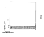
- Fig. 6 is a plan view of the solar cell 10 on the light receiving surface side.
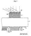
- Fig. 7 is an enlarged cross sectional view taken along the B-B line in Fig. 4 .
- the solar cell 10 includes a light reflection member 12 placed along the orthogonal direction T on one end portion of the light receiving surface of the n-type semiconductor substrate 11.
- the light reflection member 12 is arranged on the opposite side to the n-side connecting electrode 14n across the n-type semiconductor substrate 11.
- the light reflection member 12 includes a light reflecting surface 12A facing the light receiving surface protection member 2 and having light reflecting properties.
- the light reflection member 12 includes a base portion bonded onto the light receiving surface, a light reflecting layer formed on the base portion, and an oxidation/sulfuration prevention layer formed on the light reflecting layer.
- the base portion is formed of a general resin, glass, ceramic or metal material.
- a linear expansion coefficient of the base portion is preferably close to a linear expansion coefficient of the n-type semiconductor substrate 11. Having this linear expansion coefficient, the base portion can be prevented from removing from the light receiving surface of the n-type semiconductor substrate 11 due to expansion and shrinkage of the base portion along with thermal cycles.
- the light reflecting layer reflects incident light toward the light reflection member 12.
- the light reflecting layer is made of, for example, a metal material such as Ag, Al, stainless, Au, Pt, or Ni, an alloy material of any of these metal materials containing a lanthanoid such as Nd, a white resin material, or the like.
- the light reflecting layer described above gives the light reflecting properties to the light reflecting surface 12A.
- the light reflecting layer may have a thickness of approximately 100 nm.
- a bumpy structure 12B is formed in the light reflecting surface 12A as shown in Fig. 7 .
- a reflecting direction of the light reflecting surface 12A is changeable appropriately with a change in an inclination of the bumpy structure 12B.
- the incident light falling on the light reflecting surface 12A is reflected toward the other end portion of the n-type semiconductor substrate 11 by the bumpy structure 12B, and thereafter is again reflected by an interface between the light receiving surface protection member 2 and the outside air.
- the incident light falling on a region of the light receiving surface on the opposite side to the n-side connecting electrode 14n is guided to a region of the light receiving surface on the opposite side to the plurality of n-side fine-line electrodes 13n and the plurality of p-side fine-line electrodes 13p.
- the light reflection member 12 may include at least a light reflecting layer forming the light reflecting surface 12A, and may not include either the base portion or the oxidation/sulfuration prevention layer.
- the light reflecting layer may be formed directly on the light receiving surface of the n-type semiconductor substrate 11 or may be bonded onto the light receiving surface of the n-type semiconductor substrate 11.
- a substantially intrinsic amorphous semiconductor layer is formed on the almost entire back surface of the n-type semiconductor substrate 11 by using the CVD method. In this way, the passivation layer 16 is formed.
- the n-type amorphous semiconductor layer 15n is formed by using the CVD method with a predetermined region on the passivation layer 16 covered with a shadow mask.
- the p-type amorphous semiconductor layer 15p is formed by using the CVD method with a predetermined region on the passivation layer 16 covered with a shadow mask.
- ITO is sputtered on the n-type amorphous semiconductor layer 15n and the p-type amorphous semiconductor layer 15p.
- the n-side transparent conductive layer 13n 1 and the p-side transparent conductive layer 13p 1 are formed.
- a resign conductive paste for example, is printed on the n-side transparent conductive layer 13n 1 and the p-side transparent conductive layer 13p 1 . In this way, the n-side conductive layer 13n 2 and the p-side conductive layer 13p 2 are formed.
- the plurality of n-side fine-line electrodes 13n, the n-side connecting electrode 14n, the plurality of p-side fine-line electrodes 13p and the p-side connecting electrode 14p are formed on the back surface of the n-type semiconductor substrate 11.
- the light receiving surface of the n-type semiconductor substrate 11 is turned upward, and the light reflection member 12 is placed on the light receiving surface.
- the light reflection member 12 is arranged on the opposite side to the n-side connecting electrode 14n across the n-type semiconductor substrate 11.
- the plurality of solar cells 10 are formed by repeatedly performing the above steps.
- the solar cell string 1 is formed by electrically connecting the solar cells 10 to each other.
- the two solar cell strings 1 are electrically connected to each other through the bridge wiring member 5. Then, the pair of output leads 6 are respectively connected to the pair of solar cells 10 located at the two end portions of the respective two solar cell strings 1.
- the sealing member 4, the two solar cell strings 1, the sealing member 4, and the back surface protection member 3 are stacked in this order on the light receiving surface protection member 2.
- the light receiving surfaces of the n-type semiconductor substrates 11 are turned downward to face the sealing member 4.
- the sealing member 4 is heated and thereby is cured.
- the light reflection member 12 is positioned on the opposite side to the n-side connecting electrode 14n across the n-type semiconductor substrate 11.
- incident light falling on the region of the light receiving surface on the opposite side to the n-side connecting electrode 14n can be guided to the region of the light receiving surface on the opposite side to the plurality of n-side fine-line electrodes 13n and the plurality of p-side fine-line electrodes 13p.
- carrier generation is promoted in the proximity of the fine-line electrodes where the diffusion length is so short that minority carriers can be effectively collected.
- the incident light can be more effectively utilized than in the case where the incident light is absorbed by the region on the opposite side to the n-side connecting electrode 14n. Consequently, the conversion efficiency of the solar cell 10 can be improved.
- the light reflection member 12 placed on the one end portion of the n-type semiconductor substrate 11 reflects light toward the other end portion of the n-type semiconductor substrate 11.
- the incident light falling on the light reflection member 12 can be efficiently introduced into the light receiving surface of the n-type semiconductor substrate 11. For this reason, the incident light falling on the region on the opposite side to the n-side connecting electrode 14n can be more effectively utilized.
- the light receiving surface of the n-type semiconductor substrate 11 is placed to face downward.
- the solar cell string 1 does not have to be turned upside down between the two steps. Consequently, the productivity of the solar cell module 100 can be improved.
- a structure of a solar cell module according to a second embodiment in the present invention will be described by referring to the drawings. Note that, the following description is provided mainly for a different point from the aforementioned first embodiment. Specifically, a light reflection member 12 is placed over a plurality of solar cells 10.
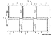
- Fig. 8 is a plan view of a solar cell string 1 according to the second embodiment when viewed from the light receiving surface side. As shown in Fig. 8 , a light reflection member 12 of one solar cell 10 and a light reflection member 12 of another solar cell 10 are formed as a single unit.
- the step of placing the light reflection member 12 on the light receiving surface of the n-type semiconductor substrate 11 can be simplified. Consequently, the productivity of the solar cell module 100 can be improved.
- the present embodiment is the same as the aforementioned first embodiment.
- a light reflection member 12 has a rectangular planar shape.
- Fig. 9 is a plan view of a solar cell string 1 according to the third embodiment when viewed from the light receiving surface side.
- a light reflection member 12 of one solar cell 10 and a light reflection member 12 of another solar cell 10 are formed integrally as a single unit.
- the integrally-formed light reflection member 12 is formed in a rectangular shape and is placed along the orthogonal direction T.
- Such light reflection members 12 can be formed by cutting a long light reflection member at predetermined intervals. Thus, the light reflection members 12 can be manufactured simply. In addition, since the light reflection member 12 is formed in a line shape, the handling properties of the light reflection members 12 can be improved.
- the n-type semiconductor substrate 11 having an n-type conductivity is used in the foregoing embodiments, but a p-type semiconductor substrate may be used.
- many of electrons (minority carriers) generated around the n-side connecting electrode 14n may be highly possibly recombined with holes (majority carriers) before being diffused into the n-side fine-line electrode 13n.
- the light reflection member 12 is arranged on the opposite side to the p-side connecting electrode 14p across the p-side semiconductor substrate.
- each of the fine-line electrodes is formed along the array direction H, and each of the connecting electrodes is formed along the orthogonal direction T.
- the structure is not limited to this.
- each of the fine-line electrodes may be formed along the orthogonal direction T and each of the connecting electrodes may be formed along the array direction H.
- the wiring members 20, the bridge wiring member 5 and the output leads 6 are each placed along the array direction H on the back surface of the n-type semiconductor substrate 11.
- the light reflection member 12 is placed along the array direction H.
- light reflection members 12 belonging to a plurality of solar cells 10 may be formed integrally as a single unit.
- each of the solar cell strings 1 is formed after the light reflection member 12 is placed on the light receiving surface of the n-type semiconductor substrate 11.
- the manufacturing method is not limited to this.
- the light reflection member 12 may be placed on the sealing member 4 and then the solar cell string 1 may be placed thereon.
- a recessed portion having such a size that the solar cell string 1 can be fitted into the recessed portion may be formed in the sealing member 4 and the light reflection member 12 may be placed in the recessed portion in advance.
- the light reflection member 12 may be bonded to the sealing member 4 in advance by preparatory bonding with the light reflection member 12 partially heated.
- a passivation layer may be formed on the light receiving surface of the n-type semiconductor substrate 11.
- An i-type amorphous semiconductor layer, a thermally-oxidized film, or the like may be used as such a passivation layer.
- a texture structure may be provided to the light receiving surface and the back surface of the n-type semiconductor substrate 11.
- a film-formation type solar cell in which the n-type amorphous semiconductor layer 15n and the p-type amorphous semiconductor layer 15p are formed on the n-type semiconductor substrate 11 by using the masks.
- a diffusion type solar cell may be used in which a p-type region and n-type region are formed inside the n-type semiconductor substrate 11.
- the n-type amorphous semiconductor layer 15n and the p-type amorphous semiconductor layer 15p are patterned by using the masks. Nevertheless, the n-type amorphous semiconductor layer 15n and the p-type amorphous semiconductor layer 15p may be patterned by using an etching paste or a resist film.
- the aforementioned embodiments use the light reflection member 12.
- a diffusion material may be used to produce the same effects.
- the bumpy structure 12B is formed in the light reflecting surface 12A.
- the structure is not limited to this.
- the light reflecting surface 12A may be formed to have a planar shape and to be inclined downward toward the other end portion of the semiconductor substrate. In this case, the light reflecting surface 12A can evenly reflect incident light toward the other end portion of the semiconductor substrate.
- the cross section of the bumpy structure 12B has an acute angled shape, but is not limited to this.
- the cross section of the bumpy structure 12B may have any shape as long as the shape allows light to be reflected well by the interface between the light receiving surface protection member 2 and the air, and may have a semicircular shape, for example.
- the solar cell module according to the present invention is usable in photovoltaic power generation since the module can effectively utilize incident light as described above.
Landscapes
- Photovoltaic Devices (AREA)
- Life Sciences & Earth Sciences (AREA)
- Engineering & Computer Science (AREA)
- Sustainable Development (AREA)
- Sustainable Energy (AREA)
Abstract
Description
- The present invention relates to a solar cell module including back junction solar cells, a solar cell and a solar cell module manufacturing method.
- Solar cells are expected as new energy sources owing to their capability of directly converting clean and inexhaustibly-supplied sunlight into electricity. In general, the output power per solar cell is several watts. Accordingly, for use of such a solar cell as a power source (energy source) for a house, a building, or the like, a solar cell module is used which is capable of providing higher output power by use of a plurality of solar cells electrically connected to each other.
- In this respect, a so-called back junction solar cell has been proposed in which a plurality of n-side fine-line electrodes and a plurality of p-side fine-line electrodes are alternately formed on a back surface of a semiconductor substrate for the purpose of enlarging a light receiving area (see Japanese Patent Application Publication No.
2005-11869 - In a case where a semiconductor substrate is of a first conductivity type, however, the connecting electrode of the first conductivity type has a problem of poor efficiency of collecting majority carriers.
- Specifically, in a solar cell including an n-type semiconductor substrate, for example, many of holes (minority carriers) generated around the n-side connecting electrode are recombined with electrons (majority carriers) before being diffused into the p-side fine-line electrodes. As a result, the number of electrons collected by the n-side connecting electrode is reduced.
- Since the first conductivity side connecting electrode cannot efficiently collect carriers as described above, incident light falling on a region of the light receiving surface on an opposite side to the first conductivity side connecting electrode cannot utilized effectively.
- The present invention has been made in consideration of the above problem, and an objective thereof is to provide a solar cell module including solar cells capable of effective use of incident light, a solar cell and a solar cell module manufacturing method.
- A solar cell module according to a feature of the present invention is summarized as a solar cell module including one solar cell sealed between a light receiving surface protection member and a back surface protection member. The one solar cell includes a semiconductor substrate of a first conductivity type having a light receiving surface and a back surface provided on an opposite side to the light receiving surface; a first conductivity side connecting electrode formed on the back surface and connected to a plurality of first conductivity side fine-line electrodes; a second conductivity side connecting electrode formed on the back surface and connected to a plurality of second conductivity side fine-line electrodes; and a light reflection member placed on the light receiving surface and having a light reflecting surface facing the light receiving surface protection member. In the one solar cell, the light reflection member is positioned on an opposite side to the first conductivity side connecting electrode across the semiconductor substrate. In the present invention, reflection means regular reflection by a mirror surface or the like, and diffused reflection by scattered reflection or the like.
- In the solar cell module according to the feature of the present invention, incident light falling on a region of the light receiving surface on the opposite side to the first conductivity side connecting electrode is guided to a region other than the region on the opposite side to the first conductivity side connecting electrode. This structure can suppress generation of photogenerated carriers in the proximity of the first conductivity side connecting electrode, and can promote generation of photogenerated carriers in the proximity of the second conductivity side connecting electrode. In the proximity of fine-line electrodes, photogenerated carriers, even minority carriers having a short diffusion length, is prevented from being recombined because the distance to the second conductivity side connecting electrode is short. Therefore, incident light falling on the region on the opposite side to the first conductivity side connecting electrode can be effectively utilized.
- In the solar cell module according to the feature of the present invention, the first conductivity side connecting electrode may be formed on one end portion of the semiconductor substrate, and the light reflection member may reflect incident light falling on the light reflection member toward another end portion of the semiconductor substrate.
- The solar cell module according to the feature of the present invention may comprise another solar cell sealed between the light receiving surface protection member and the back surface protection member, wherein the other solar cell may comprise: a semiconductor substrate of a first conductivity type having a light receiving surface and a back surface provided on an opposite side to the light receiving surface; a first conductivity side connecting electrode formed on the back surface and connected to a plurality of first conductivity side fine-line electrodes; a second conductivity side connecting electrode formed on the back surface and connected to a plurality of second conductivity side fine-line electrodes; and a light reflection member placed on the light receiving surface and having a light reflecting surface facing the light receiving surface protection member, in the other solar cell, the light reflection member may be positioned on an opposite side to the first conductivity side connecting electrode across the semiconductor substrate, and the light reflection member included in the one solar cell and the light reflection member included in the other solar cell maybe formed integrally as a single unit.
- In the solar cell module according to the feature of the present invention, the light reflecting surface may be made of any one of a metal layer and a white resin.
- In the solar cell module according to the feature of the present invention, the light reflection plate may include a base bonded to the light receiving surface.
- A solar cell according to a feature of the present invention is summarized as comprising: a semiconductor substrate of a first conductivity type having a light receiving surface and a back surface provided on an opposite side to the light receiving surface; a first conductivity side connecting electrode formed on the back surface and connected to a plurality of first conductivity side fine-line electrodes; a second conductivity side connecting electrode formed on the back surface and connected to a plurality of second conductivity side fine-line electrodes; and a light reflection member placed on the light receiving surface, and having light reflection facing the light receiving surface protection member, wherein the light reflection member is positioned on an opposite side to the first conductivity side connecting electrode across the semiconductor substrate.
- In the solar cell according to the feature of the present invention, the light reflecting surface is made of any one of a metal layer and a white resin.
- In the solar cell according to the feature of the present invention, the light reflection plate includes a base bonded to the light receiving surface.
- A method of manufacturing solar cell module according to a feature of the present invention is summarized as including one solar cell and another solar cell sealed between a light receiving surface protection member and a back surface protection member, the method comprising: a step A of forming each of the one solar cell and the other solar cell by preparing a semiconductor substrate of a first conductivity type having a back surface which is provided on an opposite side to a light receiving surface and has a first conductivity side connecting electrode and a second conductivity side connecting electrode formed thereon, with the first conductivity side connecting electrode connected to a plurality of first conductivity side fine-line electrodes, and the second conductivity side connecting electrode connected to a plurality of second conductivity side fine-line electrodes formed on the back surface, and by arranging a light reflection member on the light receiving surface of the semiconductor substrate; a step B of forming a solar cell string by electrically connecting the first conductivity side connecting electrode of the one solar cell and the second conductivity side connecting electrode of the other solar cell by use of a wiring member; and a step C of stacking a first sealing member, the solar cell string, a second sealing member and the back surface protection member in this order on the light receiving surface protection member, wherein in the step A, the light reflection member is arranged on an opposite side to the first conductivity side connecting electrode across the semiconductor substrate, and in the step B and the step C, the one solar cell and the other solar cell are placed so that the light receiving surfaces thereof face downward.
-
- [
Fig. 1] Fig. 1 is a side view of asolar cell module 100 according to a first embodiment of the present invention. - [
Fig. 2] Fig. 2 is a plan view of thesolar cell module 100 according to the first embodiment of the present invention when viewed from a back surface side. - [
Fig. 3] Fig. 3 is a plan view of thesolar cell module 100 according to the first embodiment of the present invention when viewed from a light receiving surface side. - [
Fig. 4] Fig. 4 is a plan view of the back surface side of asolar cell 10 according to the first embodiment of the present invention. - [
Fig. 5] Fig. 5 is an enlarged cross sectional view taken along a line A-A inFig. 4 . - [
Fig. 6] Fig. 6 is a plan view of a light receiving surface side of thesolar cell 10 according to the first embodiment of the present invention. - [
Fig. 7] Fig. 7 is an enlarged cross sectional view taken along a line B-B inFig. 4 . - [
Fig. 8] Fig. 8 is a plan view ofsolar cell strings 1 according to a second embodiment of the present invention when viewed from a light receiving surface side. - [
Fig. 9] Fig. 9 is a plan view ofsolar cell strings 1 according to a third embodiment of the present invention when viewed from a light receiving surface side. - [
Fig. 10] Fig. 10 is a plan view ofsolar cell strings 1 according to an embodiment of the present invention when viewed from a back surface side. - [
Fig. 11] Fig. 11 is a plan view ofsolar cell strings 1 according to an embodiment of the present invention when viewed from a receiving surface side. - [
Fig. 12] Fig. 12 is a plan view ofsolar cell strings 1 according to an embodiment of the present invention when viewed from a receiving surface side. - Hereinafter, embodiments of the present invention will be described by using the drawings. In the following description of the drawings, same or similar reference numerals denote same or similar elements and portions. In addition, it should be noted that the drawings are schematic and ratios of dimensions and the like are different from actual ones. Therefore, specific dimensions and the like should be determined in consideration of the following description. Moreover, the drawings also include portions having different dimensional relationships and ratios from one drawing to another.
- With reference to the drawings, description will be hereinbelow provided for a structure of a solar cell module according to a first embodiment of the present invention.
Fig. 1 is a side view of asolar cell module 100.Fig. 2 is a plan view ofsolar cell strings 1 when viewed from a back surface side.Fig. 3 is a plan view of thesolar cell strings 1 when viewed from a light receiving surface side. - As shown in
Figs. 1 to 3 , thesolar cell module 100 includes twosolar cell strings 1, a light receiving surface protection member 2, a backsurface protection member 3, asealing member 4, abridge wiring member 5 and a pair of output leads 6. - The two
solar cell strings 1 are sealed by the sealingmember 4 between the light receiving surface protection member 2 and the backsurface protection member 3. Each of thesolar cell strings 1 includes a plurality ofsolar cells 10 and a plurality ofwiring members 20. - The plurality of
solar cells 10 are so-called back junction solar cells each including a plurality of n-side fine-line electrodes 13n and a plurality of p-side fine-line electrodes 13p formed on a back surface of an n-type semiconductor substrate 11, as shown inFig. 2 . Thesolar cells 10 are arrayed in an array direction H. The plurality ofsolar cells 10 are electrically connected to each other through the plurality ofwiring members 20. Eachsolar cell 10 includes alight reflection member 12 placed on the light receiving surface of the n-type semiconductor substrate 11 as shown inFig. 3 . The structure of thesolar cell 10 will be described in details later. - Each of the
wiring members 20 electrically connects together onesolar cell 10 and anothersolar cell 10 next to the onesolar cell 10. Specifically, one end portion of thewiring member 20 is placed on an n-side connecting electrode 14n (seeFig. 4 ) of the onesolar cell 10. In addition, the other end portion of thewiring member 20 is placed on a p-side connecting electrode 14p (seeFig. 4 ) of the other solar cell next to the onesolar cell 10. A conductive material such as a thin-plate-shaped copper, for example, can be used as thewiring member 20. A surface of such a conductive material may be covered with a soft conductive material such as a lead-free solder (for example, SnAg3.0Cu0.5). - The light receiving surface protection member 2 protects the surface of the
solar cell module 100. A glass, a light-transmissive plastic or the like having light-transmissive and water blocking properties can be used as the light receiving surface protection member 2. - The back
surface protection member 3 protects the back surface of thesolar cell module 100. A resin film made of PET (Polyethylene Terephthalate) or the like, a laminate film having a structure in which a metal foil such as an A1 foil is sandwiched between resin films, or other similar films can be used as the backsurface protection member 3. - The sealing
member 4 seals the twosolar cell strings 1 between the light receiving surface protection member 2 and the backsurface protection member 3. A light-transmissive resin such as an EVA, EEA, PVB, silicon, urethane, acryl, or epoxy resin can be used as the sealingmember 4. - The
bridge wiring member 5 electrically connects thesolar cell strings 1 to each other. Specifically, one end portion of thebridge wiring member 5 is placed on the n-side connecting electrode 14n of thesolar cell 10 located at one end of one of the solar cell strings 1. In addition, the other end portion of thebridge wiring member 5 is placed on the p-side connecting electrode 14p of thesolar cell 10 located at one end of the othersolar cell string 1. Thebridge wiring member 5 is made of a material similar to a material for thewiring member 20. - The pair of output leads 6 output electric currents from the two
solar cell strings 1 to the outside. The pair of output leads 6 are connected to the pair ofsolar cells 10, respectively, located at two ends of the respective twosolar cell strings 1 connected together with thebridge wiring member 5. Each of the output leads 6 is made of a material similar to a material for thewiring member 20. - Incidentally, an A1 flame can be attached to an outer periphery of the
solar cell module 100 having the foregoing structure. - Hereinafter, a structure of the solar cell according to the embodiment of the present invention will be described by referring to the drawings.
Fig. 4 is a plan view of thesolar cell 10 on the back surface side.Fig. 5 is an enlarged cross sectional view taken along a line A-A inFig. 4 . - As shown in
Fig. 4 , thesolar cell 10 includes an n-type semiconductor substrate 11, a plurality of n-side fine-line electrodes 13n, a plurality of p-side fine-line electrodes 13p, an n-side connecting electrode 14n, a p-side connecting electrode 14p, an n-typeamorphous semiconductor layer 15n, a p-typeamorphous semiconductor layer 15p, and apassivation layer 16. - The n-
type semiconductor substrate 11 has a light receiving surface for receiving light and a back surface provided on the opposite side to the light receiving surface. The n-type semiconductor substrate 11 according to the present embodiment is made of a semiconductor material doped with an n-type dopant. Materials usable as such a semiconductor material are general semiconductor materials such as crystalline semiconductor materials of single-crystal Si, polycrystalline Si and the like, and compound semiconductor materials of GaAs, InP and the like. The n-type semiconductor substrate 11 generates photogenerated carriers (holes and electrons) by receiving light. Here, since the conductivity of the n-type semiconductor substrate 11 is n type, the photogenerated carriers includes the electrons as majority carriers and the holes as minority carriers. - The plurality of n-side fine-
line electrodes 13n are collecting electrodes that collect the electrons from the n-type semiconductor substrate 11. Each of the n-side fine-line electrodes 13n is formed along the array direction H on the back surface of the n-type semiconductor substrate 11 as shown inFig. 4 . - The plurality of p-side fine-
line electrodes 13p are collecting electrodes that collect the holes from the n-type semiconductor substrate 11. The p-side fine-line electrodes 13p are formed along the n-side fine-line electrodes 13n on the back surface of the n-type semiconductor substrate 11 as shown inFig. 4 . The n-side fine-line electrodes 13n and the p-side fine-line electrodes 13p are formed alternately into a form of stripes. - Note that, as shown in
Fig. 5 , each of the n-side fine-line electrodes 13n includes an n-side transparentconductive layer 13n1 and an n-sideconductive layer 13n2. The n-sideconductive layer 13n2 is formed on the n-side transparentconductive layer 13n1. The n-side transparentconductive layer 13n1 is formed on the n-typeamorphous semiconductor layer 15n. The n-side transparentconductive layer 13n1 is formed of an oxide of In, Zn, Sn, Ti, W or the like. The n-sideconductive layer 13n2 is formed of silver, a resin conductive paste or a sintered conductive paste. - Moreover, as shown in
Fig. 5 , each of the p-side fine-line electrodes 13p includes a p-side transparentconductive layer 13p1 and a p-sideconductive layer 13p2. The p-sideconductive layer 13p2 is formed on the p-side transparentconductive layer 13p1. The p-side transparentconductive layer 13p1 is formed on the p-typeamorphous semiconductor layer 15p. The p-side transparentconductive layer 13p1 is formed of an oxide of In, Zn, Sn, Ti, W or the like. The p-sideconductive layer 13p2 is formed of silver, a resin conductive paste or a sintered conductive paste. - The n-
side connecting electrode 14n is formed along an orthogonal direction T substantially orthogonal to the array direction H, on one end portion of the n-type semiconductor substrate 11, as shown inFig. 4 . The n-side connecting electrode 14n is connected to the plurality of n-side fine-line electrodes 13n. The n-side connecting electrode 14n is an electrode to which thewiring member 20, thebridge wiring member 5, or theoutput lead 6 is to be connected. Moreover, the n-side connecting electrode 14n is a collecting electrode for collecting electrons from the n-type semiconductor substrate 11. - The p-
side connecting electrode 14p is formed along the orthogonal direction T on another end portion of the n-type semiconductor substrate 11, as shown inFig. 4 . The p-side connecting electrode 14p is connected to the plurality of p-side fine-line electrodes 13p. The p-side connecting electrode 14p is an electrode to which thewiring member 20, thebridge wiring member 5, or theoutput lead 6 is to be connected. Moreover, the p-side connecting electrode 14p is a collecting electrode for collecting holes from the n-type semiconductor substrate 11. - Here, the n-
side connecting electrode 14n has a structure similar to the structure of the n-side fine-line electrodes 13n (seeFig. 7 ) . In addition, the p-side connecting electrode 14p has a structure similar to the structure of the p-side fine-line electrodes 13p, though not illustrated. - As shown in
Fig. 4 , the n-typeamorphous semiconductor layer 15n is formed in a comb-like shape on the back surface of the n-type semiconductor substrate 11. The plurality of n-side fine-line electrodes 13n each extending in the array direction H and the n-side connecting electrode 14n extending in the orthogonal direction T are provided on the n-typeamorphous semiconductor layer 15n. - As shown in
Fig. 4 , the p-typeamorphous semiconductor layer 15p is formed in a comb-like shape on the back surface of the n-type semiconductor substrate 11. The plurality of p-side fine-line electrodes 13p each extending along the array direction H and the p-side connecting electrode 14p extending along the orthogonal direction T are provided on the p-typeamorphous semiconductor layer 15p. - Note that, as shown in
Fig. 5 , the n-typeamorphous semiconductor layer 15n and the p-typeamorphous semiconductor layer 15p are formed on thepassivation layer 16. - As shown in
Fig. 4 , thepassivation layer 16 is formed to almost entirely cover the back surface of the n-type semiconductor substrate 11. The passivation layer 16 a substantially intrinsic amorphous semiconductor layer (i-type amorphous semiconductor layer) formed without doping of any dopant or with doping of a very small amount of dopant. Thepassivation layer 16 has passivating properties of inhibiting recombining of carriers. - Here,
Fig. 6 is a plan view of thesolar cell 10 on the light receiving surface side.Fig. 7 is an enlarged cross sectional view taken along the B-B line inFig. 4 . - As shown in
Fig. 6 , thesolar cell 10 includes alight reflection member 12 placed along the orthogonal direction T on one end portion of the light receiving surface of the n-type semiconductor substrate 11. As shown inFig. 7 , thelight reflection member 12 is arranged on the opposite side to the n-side connecting electrode 14n across the n-type semiconductor substrate 11. Thelight reflection member 12 includes alight reflecting surface 12A facing the light receiving surface protection member 2 and having light reflecting properties. - In the present embodiment, the
light reflection member 12 includes a base portion bonded onto the light receiving surface, a light reflecting layer formed on the base portion, and an oxidation/sulfuration prevention layer formed on the light reflecting layer. - The base portion is formed of a general resin, glass, ceramic or metal material. A linear expansion coefficient of the base portion is preferably close to a linear expansion coefficient of the n-
type semiconductor substrate 11. Having this linear expansion coefficient, the base portion can be prevented from removing from the light receiving surface of the n-type semiconductor substrate 11 due to expansion and shrinkage of the base portion along with thermal cycles. - The light reflecting layer reflects incident light toward the
light reflection member 12. The light reflecting layer is made of, for example, a metal material such as Ag, Al, stainless, Au, Pt, or Ni, an alloy material of any of these metal materials containing a lanthanoid such as Nd, a white resin material, or the like. The light reflecting layer described above gives the light reflecting properties to thelight reflecting surface 12A. Incidentally, in the case of the light reflecting layer made of any of the above metal material, the light reflecting layer may have a thickness of approximately 100 nm. - Here, in the present embodiment, a
bumpy structure 12B is formed in thelight reflecting surface 12A as shown inFig. 7 . A reflecting direction of thelight reflecting surface 12A is changeable appropriately with a change in an inclination of thebumpy structure 12B. In the present embodiment, the incident light falling on thelight reflecting surface 12A is reflected toward the other end portion of the n-type semiconductor substrate 11 by thebumpy structure 12B, and
thereafter is again reflected by an interface between the light receiving surface protection member 2 and the outside air. With this, the incident light falling on a region of the light receiving surface on the opposite side to the n-side connecting electrode 14n is guided to a region of the light receiving surface on the opposite side to the plurality of n-side fine-line electrodes 13n and the plurality of p-side fine-line electrodes 13p. - Incidentally, the
light reflection member 12 may include at least a light reflecting layer forming thelight reflecting surface 12A, and may not include either the base portion or the oxidation/sulfuration prevention layer. In this case, the light reflecting layer may be formed directly on the light receiving surface of the n-type semiconductor substrate 11 or may be bonded onto the light receiving surface of the n-type semiconductor substrate 11. - Next, a manufacturing method of the
solar cell module 100 is described. - First of all, a substantially intrinsic amorphous semiconductor layer is formed on the almost entire back surface of the n-
type semiconductor substrate 11 by using the CVD method. In this way, thepassivation layer 16 is formed. - Then, the n-type
amorphous semiconductor layer 15n is formed by using the CVD method with a predetermined region on thepassivation layer 16 covered with a shadow mask. Subsequently, the p-typeamorphous semiconductor layer 15p is formed by using the CVD method with a predetermined region on thepassivation layer 16 covered with a shadow mask. - Thereafter, ITO, for example, is sputtered on the n-type
amorphous semiconductor layer 15n and the p-typeamorphous semiconductor layer 15p. In this way, the n-side transparentconductive layer 13n1 and the p-side transparentconductive layer 13p1 are formed. After that, a resign conductive paste, for example, is printed on the n-side transparentconductive layer 13n1 and the p-side transparentconductive layer 13p1. In this way, the n-sideconductive layer 13n2 and the p-sideconductive layer 13p2 are formed. In this way, the plurality of n-side fine-line electrodes 13n, the n-side connecting electrode 14n, the plurality of p-side fine-line electrodes 13p and the p-side connecting electrode 14p are formed on the back surface of the n-type semiconductor substrate 11. - Subsequently, the light receiving surface of the n-
type semiconductor substrate 11 is turned upward, and thelight reflection member 12 is placed on the light receiving surface. In this case, thelight reflection member 12 is arranged on the opposite side to the n-side connecting electrode 14n across the n-type semiconductor substrate 11. - The plurality of
solar cells 10 are formed by repeatedly performing the above steps. - Then, the light receiving surface of the n-
type semiconductor substrate 11 is turned downward and thewiring members 20 are connected to the back surface of the n-type semiconductor substrate 11. Thesolar cell string 1 is formed by electrically connecting thesolar cells 10 to each other. - Next, the two
solar cell strings 1 are electrically connected to each other through thebridge wiring member 5. Then, the pair of output leads 6 are respectively connected to the pair ofsolar cells 10 located at the two end portions of the respective two solar cell strings 1. - Subsequently, the sealing
member 4, the twosolar cell strings 1, the sealingmember 4, and the backsurface protection member 3 are stacked in this order on the light receiving surface protection member 2. In this case, the light receiving surfaces of the n-type semiconductor substrates 11 are turned downward to face the sealingmember 4. - Next, the sealing
member 4 is heated and thereby is cured. - In the
solar cell module 100 according to the present embodiment, thelight reflection member 12 is positioned on the opposite side to the n-side connecting electrode 14n across the n-type semiconductor substrate 11. - Hence, incident light falling on the region of the light receiving surface on the opposite side to the n-
side connecting electrode 14n can be guided to the region of the light receiving surface on the opposite side to the plurality of n-side fine-line electrodes 13n and the plurality of p-side fine-line electrodes 13p. Thus, carrier generation is promoted in the proximity of the fine-line electrodes where the diffusion length is so short that minority carriers can be effectively collected. For this reason, the incident light can be more effectively utilized than in the case where the incident light is absorbed by the region on the opposite side to the n-side connecting electrode 14n. Consequently, the conversion efficiency of thesolar cell 10 can be improved. - In addition, in the present embodiment, the
light reflection member 12 placed on the one end portion of the n-type semiconductor substrate 11 reflects light toward the other end portion of the n-type semiconductor substrate 11. Thus, the incident light falling on thelight reflection member 12 can be efficiently introduced into the light receiving surface of the n-type semiconductor substrate 11. For this reason, the incident light falling on the region on the opposite side to the n-side connecting electrode 14n can be more effectively utilized. - Moreover, in the present embodiment, in the step of forming the
solar cell string 1 and the step of placing the two solar cell strings on the sealingmember 4, the light receiving surface of the n-type semiconductor substrate 11 is placed to face downward. Thus, thesolar cell string 1 does not have to be turned upside down between the two steps. Consequently, the productivity of thesolar cell module 100 can be improved. - Hereinafter, a structure of a solar cell module according to a second embodiment in the present invention will be described by referring to the drawings. Note that, the following description is provided mainly for a different point from the aforementioned first embodiment. Specifically, a
light reflection member 12 is placed over a plurality ofsolar cells 10. -
Fig. 8 is a plan view of asolar cell string 1 according to the second embodiment when viewed from the light receiving surface side. As shown inFig. 8 , alight reflection member 12 of onesolar cell 10 and alight reflection member 12 of anothersolar cell 10 are formed as a single unit. - Accordingly, the step of placing the
light reflection member 12 on the light receiving surface of the n-type semiconductor substrate 11 can be simplified. Consequently, the productivity of thesolar cell module 100 can be improved. - Note that, in terms of the structure and other points of the
solar cell 10, the present embodiment is the same as the aforementioned first embodiment. - Hereinafter, a structure of a solar cell module according to a third embodiment in the present invention will be described by referring to the drawings. Note that, the following description is provided mainly for a different point from the aforementioned second embodiment. Specifically, a
light reflection member 12 has a rectangular planar shape. -
Fig. 9 is a plan view of asolar cell string 1 according to the third embodiment when viewed from the light receiving surface side. As shown inFig. 9 , alight reflection member 12 of onesolar cell 10 and alight reflection member 12 of anothersolar cell 10 are formed integrally as a single unit. In addition, the integrally-formedlight reflection member 12 is formed in a rectangular shape and is placed along the orthogonal direction T. - Such
light reflection members 12 can be formed by cutting a long light reflection member at predetermined intervals. Thus, thelight reflection members 12 can be manufactured simply. In addition, since thelight reflection member 12 is formed in a line shape, the handling properties of thelight reflection members 12 can be improved. - As described above, the details of the present invention have been disclosed by using the embodiments of the present invention. However, it should not be understood that the description and drawings which constitute part of this disclosure limit the present invention. From this disclosure, various alternative embodiments, examples, and operation techniques will be easily found by those skilled in the art.
- For example, the n-
type semiconductor substrate 11 having an n-type conductivity is used in the foregoing embodiments, but a p-type semiconductor substrate may be used. In this case, many of electrons (minority carriers) generated around the n-side connecting electrode 14n may be highly possibly recombined with holes (majority carriers) before being diffused into the n-side fine-line electrode 13n. For this reason, thelight reflection member 12 is arranged on the opposite side to the p-side connecting electrode 14p across the p-side semiconductor substrate. - Additionally, in the foregoing embodiments, each of the fine-line electrodes is formed along the array direction H, and each of the connecting electrodes is formed along the orthogonal direction T. However, the structure is not limited to this. For example, each of the fine-line electrodes may be formed along the orthogonal direction T and each of the connecting electrodes may be formed along the array direction H. To be more specific, as shown in
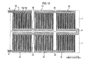
Fig. 10 , thewiring members 20, thebridge wiring member 5 and the output leads 6 are each placed along the array direction H on the back surface of the n-type semiconductor substrate 11. In addition, as shown inFig. 11 , thelight reflection member 12 is placed along the array direction H. In this case, as shown inFig. 12 ,light reflection members 12 belonging to a plurality ofsolar cells 10 may be formed integrally as a single unit. - Moreover, in the aforementioned embodiments, each of the
solar cell strings 1 is formed after thelight reflection member 12 is placed on the light receiving surface of the n-type semiconductor substrate 11. However, the manufacturing method is not limited to this. For example, thelight reflection member 12 may be placed on the sealingmember 4 and then thesolar cell string 1 may be placed thereon. In this case, a recessed portion having such a size that thesolar cell string 1 can be fitted into the recessed portion may be formed in the sealingmember 4 and thelight reflection member 12 may be placed in the recessed portion in advance. Here, thelight reflection member 12 may be bonded to the sealingmember 4 in advance by preparatory bonding with thelight reflection member 12 partially heated. - In addition, though not particularly mentioned in the foregoing embodiments, a passivation layer may be formed on the light receiving surface of the n-
type semiconductor substrate 11. An i-type amorphous semiconductor layer, a thermally-oxidized film, or the like may be used as such a passivation layer. - Further, though not particularly mentioned in the foregoing embodiments, a texture structure may be provided to the light receiving surface and the back surface of the n-
type semiconductor substrate 11. - Additionally, the foregoing embodiments have been described by taking as an example a film-formation type solar cell in which the n-type
amorphous semiconductor layer 15n and the p-typeamorphous semiconductor layer 15p are formed on the n-type semiconductor substrate 11 by using the masks. However, a diffusion type solar cell may be used in which a p-type region and n-type region are formed inside the n-type semiconductor substrate 11. - Moreover, in the foregoing embodiments, the n-type
amorphous semiconductor layer 15n and the p-typeamorphous semiconductor layer 15p are patterned by using the masks. Nevertheless, the n-typeamorphous semiconductor layer 15n and the p-typeamorphous semiconductor layer 15p may be patterned by using an etching paste or a resist film. - Further, the aforementioned embodiments use the
light reflection member 12. However, a diffusion material may be used to produce the same effects. - Furthermore, in the foregoing embodiments, the
bumpy structure 12B is formed in thelight reflecting surface 12A. The structure, however, is not limited to this. For example, thelight reflecting surface 12A may be formed to have a planar shape and to be inclined downward toward the other end portion of the semiconductor substrate. In this case, thelight reflecting surface 12A can evenly reflect incident light toward the other end portion of the semiconductor substrate. - Still further, in the foregoing embodiments, the cross section of the
bumpy structure 12B has an acute angled shape, but is not limited to this. The cross section of thebumpy structure 12B may have any shape as long as the shape allows light to be reflected well by the interface between the light receiving surface protection member 2 and the air, and may have a semicircular shape, for example. - As described above, the present invention naturally includes various embodiments which are not described herein. Accordingly, the technical scope of the present invention should be determined only by the matters to define the invention in the scope of claims regarded as appropriate based on the description.
- Note that the entire content of Japanese Patent Application No.
2008-214525 (filed on August 22, 2008 - The solar cell module according to the present invention is usable in photovoltaic power generation since the module can effectively utilize incident light as described above.
Claims (9)
- A solar cell module comprising one solar cell sealed between a light receiving surface protection member and a back surface protection member, wherein,
the one solar cell comprises:a semiconductor substrate of a first conductivity type having a light receiving surface and a back surface provided on an opposite side to the light receiving surface;a first conductivity side connecting electrode formed on the back surface and connected to a plurality of first conductivity side fine-line electrodes;a second conductivity side connecting electrode formed on the back surface and connected to a plurality of second conductivity side fine-line electrodes; anda light reflection member placed on the light receiving surface and having a light reflecting surface facing the light receiving surface protection member, andin the one solar cell, the light reflection member is positioned on an opposite side to the first conductivity side connecting electrode across the semiconductor substrate. - The solar cell module according to claim 1, wherein the first conductivity side connecting electrode is formed on one end portion of the semiconductor substrate, and
the light reflection member reflects incident light falling on the light reflection member toward another end portion of the semiconductor substrate. - The solar cell module according to any one of claims 1 and 2, comprising another solar cell sealed between the light receiving surface protection member and the back surface protection member, wherein
the other solar cell comprises:a semiconductor substrate of a first conductivity type having a light receiving surface and a back surface provided on an opposite side to the light receiving surface;a first conductivity side connecting electrode formed on the back surface and connected to a plurality of first conductivity side fine-line electrodes;a second conductivity side connecting electrode formed on the back surface and connected to a plurality of second conductivity side fine-line electrodes; anda light reflection member placed on the light receiving surface and having a light reflecting surface facing the light receiving surface protection member,in the other solar cell, the light reflection member is positioned on an opposite side to the first conductivity side connecting electrode across the semiconductor substrate, and
the light reflection member included in the one solar cell and the light reflection member included in the other solar cell are formed integrally as a single unit. - The solar cell module according to any one of claims 1 to 3, wherein
the light reflecting surface is made of any one of a metal layer and a white resin. - The solar cell module according to any one of claims 1 to 4, wherein the light reflection plate includes a base bonded to the light receiving surface.
- A solar cell comprising:a semiconductor substrate of a first conductivity type having a light receiving surface and a back surface provided on an opposite side to the light receiving surface;a first conductivity side connecting electrode formed on the back surface and connected to a plurality of first conductivity side fine-line electrodes;a second conductivity side connecting electrode formed on the back surface and connected to a plurality of second conductivity side fine-line electrodes; anda light reflection member placed on the light receiving surface, and having light reflection facing the light receiving surface protection member, whereinthe light reflection member is positioned on an opposite side to the first conductivity side connecting electrode across the semiconductor substrate.
- The solar cell according to claim 6, wherein the light reflecting surface is made of any one of a metal layer and a white resin.
- The solar cell according to any one of claims 6 and 7, wherein the light reflection plate includes a base bonded to the light receiving surface.
- A method of manufacturing a solar cell module including one solar cell and another solar cell sealed between a light receiving surface protection member and a back surface protection member, the method comprising:a step A of forming each of the one solar cell and the other solar cell by preparing a semiconductor substrate of a first conductivity type having a back surface which is provided on an opposite side to a light receiving surface and has a first conductivity side connecting electrode and a second conductivity side connecting electrode formed thereon, with the first conductivity side connecting electrode connected to a plurality of first conductivity side fine-line electrodes, and the second conductivity side connecting electrode connected to a plurality of second conductivity side fine-line electrodes formed on the back surface, and by arranging a light reflection member on the light receiving surface of the semiconductor substrate;a step B of forming a solar cell string by electrically connecting the first conductivity side connecting electrode of the one solar cell and the second conductivity side connecting electrode of the other solar cell by use of a wiring member; anda step C of stacking a first sealing member, the solar cell string, a second sealing member and the back surface protection member in this order on the light receiving surface protection member, whereinin the step A, the light reflection member is arranged on an opposite side to the first conductivity side connecting electrode across the semiconductor substrate, andin the step B and the step C, the one solar cell and the other solar cell are placed so that the light receiving surfaces thereof face downward.
Applications Claiming Priority (2)
| Application Number | Priority Date | Filing Date | Title |
|---|---|---|---|
| JP2008214525 | 2008-08-22 | ||
| PCT/JP2009/061848 WO2010021204A1 (en) | 2008-08-22 | 2009-06-29 | Solar cell module, solar cell, and solar cell module manufacturing method |
Publications (2)
| Publication Number | Publication Date |
|---|---|
| EP2320477A1 true EP2320477A1 (en) | 2011-05-11 |
| EP2320477A4 EP2320477A4 (en) | 2012-08-08 |
Family
ID=41707083
Family Applications (1)
| Application Number | Title | Priority Date | Filing Date |
|---|---|---|---|
| EP09808140A Withdrawn EP2320477A4 (en) | 2008-08-22 | 2009-06-29 | SOLAR CELL MODULE, SOLAR CELL, AND METHOD FOR MANUFACTURING SOLAR CELL MODULE |
Country Status (5)
| Country | Link |
|---|---|
| US (1) | US9252299B2 (en) |
| EP (1) | EP2320477A4 (en) |
| JP (1) | JP5306352B2 (en) |
| CN (1) | CN102132420A (en) |
| WO (1) | WO2010021204A1 (en) |
Cited By (3)
| Publication number | Priority date | Publication date | Assignee | Title |
|---|---|---|---|---|
| CN102790110A (en) * | 2011-05-18 | 2012-11-21 | Lg电子株式会社 | Solar cell module |
| EP2869350A1 (en) * | 2013-10-29 | 2015-05-06 | LG Electronics Inc. | Solar cell module |
| EP3715961A1 (en) * | 2019-03-26 | 2020-09-30 | Casio Computer Co., Ltd. | Solar panel for a timepiece |
Families Citing this family (32)
| Publication number | Priority date | Publication date | Assignee | Title |
|---|---|---|---|---|
| DE102010004439A1 (en) * | 2010-01-05 | 2011-07-07 | Steinbeis-Transferzentrum Angewandte Photovoltaik u. Dünnschichttechnik, 70197 | solar cell module |
| JP5424270B2 (en) * | 2010-05-11 | 2014-02-26 | 国立大学法人東京農工大学 | Semiconductor solar cell |
| KR101699297B1 (en) * | 2010-09-08 | 2017-02-13 | 엘지전자 주식회사 | Method for manufacturing solar cell |
| JP2012142456A (en) * | 2010-12-29 | 2012-07-26 | Sanyo Electric Co Ltd | Solar battery, solar battery module, and manufacturing method of the solar battery module |
| JP5842170B2 (en) * | 2011-06-23 | 2016-01-13 | パナソニックIpマネジメント株式会社 | Solar cell module |
| EP2731147B1 (en) * | 2011-07-04 | 2021-03-24 | Panasonic Intellectual Property Management Co., Ltd. | Solar cell module |
| EP2752889B1 (en) * | 2011-08-31 | 2018-11-28 | Panasonic Intellectual Property Management Co., Ltd. | Method for producing solar cell module |
| WO2013042683A1 (en) * | 2011-09-20 | 2013-03-28 | 三洋電機株式会社 | Solar cell module |
| JP5950154B2 (en) * | 2012-05-09 | 2016-07-13 | パナソニックIpマネジメント株式会社 | Solar cell module |
| TWI643351B (en) * | 2013-01-31 | 2018-12-01 | 澳洲商新南創新有限公司 | Solar cell metallization and interconnection method |
| WO2014162790A1 (en) * | 2013-04-05 | 2014-10-09 | 三菱電機株式会社 | Photoelectric conversion apparatus |
| DE112014004490T5 (en) * | 2013-09-30 | 2016-09-01 | Panasonic Intellectual Property Management Co., Ltd. | Solar cell module and solar cell module manufacturing process |
| JP6429032B2 (en) | 2014-02-06 | 2018-11-28 | パナソニックIpマネジメント株式会社 | Solar cell module and method for manufacturing solar cell module |
| WO2015118592A1 (en) * | 2014-02-06 | 2015-08-13 | パナソニックIpマネジメント株式会社 | Solar cell and solar cell manufacturing method |
| KR102271055B1 (en) * | 2014-06-26 | 2021-07-01 | 엘지전자 주식회사 | Solar cell module |
| US9559233B2 (en) * | 2014-09-25 | 2017-01-31 | Sunpower Corporation | Solar cell interconnection |
| CN104282788B (en) * | 2014-09-28 | 2017-03-22 | 苏州中来光伏新材股份有限公司 | Main-grid-free high-efficiency back contact solar cell module, main-grid-free high-efficiency back contact solar cell assembly and manufacturing technology of main-grid-free high-efficiency back contact solar cell assembly |
| WO2016143250A1 (en) * | 2015-03-10 | 2016-09-15 | パナソニックIpマネジメント株式会社 | Solar battery module production method |
| JP6384801B2 (en) * | 2015-03-11 | 2018-09-05 | パナソニックIpマネジメント株式会社 | Solar cell module |
| JP6624418B2 (en) | 2015-03-13 | 2019-12-25 | パナソニックIpマネジメント株式会社 | Solar cell module |
| WO2016147924A1 (en) | 2015-03-13 | 2016-09-22 | シャープ株式会社 | Photoelectric conversion element and photoelectric conversion module |
| WO2016157695A1 (en) * | 2015-03-31 | 2016-10-06 | パナソニックIpマネジメント株式会社 | Solar cell element, solar cell module, and method for manufacturing solar cell element |
| US11195966B2 (en) * | 2015-09-11 | 2021-12-07 | Sunpower Corporation | Bifacial solar cells with reflective back contacts |
| WO2017056371A1 (en) * | 2015-09-30 | 2017-04-06 | パナソニックIpマネジメント株式会社 | Solar cell module and method for producing solar cell |
| JP6352894B2 (en) * | 2015-12-24 | 2018-07-04 | トヨタ自動車株式会社 | Solar cell module |
| KR101823601B1 (en) * | 2017-01-17 | 2018-01-30 | 엘지전자 주식회사 | Solar cell module |
| JP6986357B2 (en) * | 2017-03-24 | 2021-12-22 | 株式会社カネカ | Solar cell module |
| CN111630666B (en) * | 2018-01-24 | 2023-11-07 | 株式会社钟化 | Connecting component set for solar cell units, and solar cell strings and solar cell modules using the connecting component set |
| JP2019133985A (en) | 2018-01-29 | 2019-08-08 | パナソニック株式会社 | Photovoltaic cell and method for manufacturing the same |
| CN115943501B (en) * | 2020-07-20 | 2026-07-03 | 株式会社钟化 | Solar cell module |
| CN115777149B (en) | 2020-08-06 | 2025-12-19 | 株式会社钟化 | Solar cell and method for manufacturing solar cell |
| CN116404050A (en) * | 2023-04-24 | 2023-07-07 | 晶科能源(海宁)有限公司 | Back-contact photovoltaic module and manufacturing method thereof |
Family Cites Families (16)
| Publication number | Priority date | Publication date | Assignee | Title |
|---|---|---|---|---|
| JPS5610976A (en) | 1979-07-09 | 1981-02-03 | Agency Of Ind Science & Technol | Photoelectric converter |
| US4838952A (en) * | 1988-04-29 | 1989-06-13 | Spectrolab, Inc. | Controlled reflectance solar cell |
| JP3070489B2 (en) | 1996-10-09 | 2000-07-31 | トヨタ自動車株式会社 | Concentrating solar cell element |
| EP0881694A1 (en) * | 1997-05-30 | 1998-12-02 | Interuniversitair Micro-Elektronica Centrum Vzw | Solar cell and process of manufacturing the same |
| US7220997B2 (en) * | 2002-06-21 | 2007-05-22 | Josuke Nakata | Light receiving or light emitting device and itsd production method |
| JP2005011869A (en) * | 2003-06-17 | 2005-01-13 | Sekisui Jushi Co Ltd | Solar cell module and its manufacturing method |
| TW200642103A (en) * | 2005-03-31 | 2006-12-01 | Sanyo Electric Co | Solar battery module |
| US20070095384A1 (en) * | 2005-10-28 | 2007-05-03 | Farquhar Donald S | Photovoltaic modules and interconnect methodology for fabricating the same |
| JP2007281044A (en) | 2006-04-04 | 2007-10-25 | Canon Inc | Solar cell |
| JP2007281156A (en) * | 2006-04-06 | 2007-10-25 | Japan Advanced Institute Of Science & Technology Hokuriku | Back-electrode-type semiconductor heterojunction solar cell and method and apparatus for manufacturing the same |
| JP2008091697A (en) | 2006-10-03 | 2008-04-17 | Toyota Motor Corp | Photovoltaic element |
| EP2104147B1 (en) | 2006-12-26 | 2015-04-15 | Kyocera Corporation | Solar cell element and solar cell element manufacturing method |
| WO2008090718A1 (en) * | 2007-01-25 | 2008-07-31 | Sharp Kabushiki Kaisha | Solar battery cell, solar battery array, solar battery module and method for manufacturing solar battery array |
| JP2008282926A (en) * | 2007-05-09 | 2008-11-20 | Sanyo Electric Co Ltd | Solar cell module |
| JP2009088203A (en) * | 2007-09-28 | 2009-04-23 | Sanyo Electric Co Ltd | SOLAR CELL, SOLAR CELL MODULE, AND SOLAR CELL MANUFACTURING METHOD |
| JP2009135338A (en) * | 2007-11-30 | 2009-06-18 | Sanyo Electric Co Ltd | Solar cell and method for manufacturing solar cell |
-
2009
- 2009-06-29 EP EP09808140A patent/EP2320477A4/en not_active Withdrawn
- 2009-06-29 US US13/060,233 patent/US9252299B2/en not_active Expired - Fee Related
- 2009-06-29 JP JP2010525635A patent/JP5306352B2/en not_active Expired - Fee Related
- 2009-06-29 CN CN2009801327643A patent/CN102132420A/en active Pending
- 2009-06-29 WO PCT/JP2009/061848 patent/WO2010021204A1/en not_active Ceased
Cited By (11)
| Publication number | Priority date | Publication date | Assignee | Title |
|---|---|---|---|---|
| CN102790110A (en) * | 2011-05-18 | 2012-11-21 | Lg电子株式会社 | Solar cell module |
| EP2525415A3 (en) * | 2011-05-18 | 2013-12-25 | LG Electronics Inc. | Solar cell module |
| CN102790110B (en) * | 2011-05-18 | 2015-06-24 | Lg电子株式会社 | Solar cell module |
| US9768336B2 (en) | 2011-05-18 | 2017-09-19 | Lg Electronics Inc. | Solar cell module |
| US10236403B2 (en) | 2011-05-18 | 2019-03-19 | Lg Electronics Inc. | Solar cell module |
| EP2869350A1 (en) * | 2013-10-29 | 2015-05-06 | LG Electronics Inc. | Solar cell module |
| US9799782B2 (en) | 2013-10-29 | 2017-10-24 | Lg Electronics Inc. | Solar cell module and method for manufacturing the same |
| US10636921B2 (en) | 2013-10-29 | 2020-04-28 | Lg Electronics Inc. | Solar cell module and method for manufacturing the same |
| EP3715961A1 (en) * | 2019-03-26 | 2020-09-30 | Casio Computer Co., Ltd. | Solar panel for a timepiece |
| CN111834482A (en) * | 2019-03-26 | 2020-10-27 | 卡西欧计算机株式会社 | Solar panels, display devices and clocks |
| US11803160B2 (en) | 2019-03-26 | 2023-10-31 | Casio Computer Co., Ltd. | Solar panel, display, and timepiece |
Also Published As
| Publication number | Publication date |
|---|---|
| JPWO2010021204A1 (en) | 2012-01-26 |
| US20110277817A1 (en) | 2011-11-17 |
| EP2320477A4 (en) | 2012-08-08 |
| US9252299B2 (en) | 2016-02-02 |
| WO2010021204A1 (en) | 2010-02-25 |
| JP5306352B2 (en) | 2013-10-02 |
| CN102132420A (en) | 2011-07-20 |
Similar Documents
| Publication | Publication Date | Title |
|---|---|---|
| US9252299B2 (en) | Solar cell module, solar cell and solar cell module manufacturing method | |
| JP7564974B2 (en) | Photovoltaic cells and photovoltaic modules | |
| JP5410050B2 (en) | Solar cell module | |
| KR101537116B1 (en) | Solar cell module | |
| US10090428B2 (en) | Solar cell and method for manufacturing the same | |
| EP4665119A1 (en) | Solar cell and tandem solar cell | |
| CN218585994U (en) | Solar cell and photovoltaic module | |
| CN102157612B (en) | Solar cell and manufacturing method thereof | |
| WO2008059593A1 (en) | Stacked solar cell device | |
| JP5496473B2 (en) | Back electrode type solar cell, solar cell string and solar cell module | |
| EP4629783B1 (en) | Solar cell, tandem solar cell and photovoltaic module | |
| EP4633329A1 (en) | Segmented solar cell, method for forming the same and photovoltaic module | |
| US20200203540A1 (en) | Solar cell and electronic device provided with said solar cell | |
| CN119521854B (en) | Back contact solar cells and photovoltaic modules | |
| US20200313010A1 (en) | Solar cell and solar cell module | |
| KR20230038356A (en) | SOLAR CELL, the Manufacturing method thereof, and SOLAR CELL MODULE having the same | |
| US20250338668A1 (en) | Solar cell and photovoltaic module | |
| JP2010283406A (en) | Solar cell | |
| US20200168751A1 (en) | Solar cell and solar cell module | |
| US8772079B2 (en) | Backside contacting on thin layer photovoltaic cells | |
| JP2006013173A (en) | Solar cell module | |
| US20090056796A1 (en) | Structure Of An Edge Conducting Double-Sided Flip-Chip Solar Cell | |
| JP5722413B2 (en) | Back electrode type solar cell, solar cell string and solar cell module | |
| JP2019004189A (en) | Photoelectric conversion device |
Legal Events
| Date | Code | Title | Description |
|---|---|---|---|
| PUAI | Public reference made under article 153(3) epc to a published international application that has entered the european phase |
Free format text: ORIGINAL CODE: 0009012 |
|
| 17P | Request for examination filed |
Effective date: 20110308 |
|
| AK | Designated contracting states |
Kind code of ref document: A1 Designated state(s): AT BE BG CH CY CZ DE DK EE ES FI FR GB GR HR HU IE IS IT LI LT LU LV MC MK MT NL NO PL PT RO SE SI SK TR |
|
| AX | Request for extension of the european patent |
Extension state: AL BA RS |
|
| DAX | Request for extension of the european patent (deleted) | ||
| A4 | Supplementary search report drawn up and despatched |
Effective date: 20120705 |
|
| RIC1 | Information provided on ipc code assigned before grant |
Ipc: H01L 31/0224 20060101ALI20120629BHEP Ipc: H01L 31/052 20060101ALI20120629BHEP Ipc: H01L 31/048 20060101ALI20120629BHEP Ipc: H01L 31/072 20120101ALI20120629BHEP Ipc: H01L 31/04 20060101ALI20120629BHEP Ipc: H01L 31/042 20060101AFI20120629BHEP Ipc: H01L 31/0236 20060101ALI20120629BHEP Ipc: H01L 31/05 20060101ALI20120629BHEP |
|
| STAA | Information on the status of an ep patent application or granted ep patent |
Free format text: STATUS: THE APPLICATION IS DEEMED TO BE WITHDRAWN |
|
| 18D | Application deemed to be withdrawn |
Effective date: 20130205 |