EP2320134A2 - Lighting device - Google Patents
Lighting device Download PDFInfo
- Publication number
- EP2320134A2 EP2320134A2 EP10190498A EP10190498A EP2320134A2 EP 2320134 A2 EP2320134 A2 EP 2320134A2 EP 10190498 A EP10190498 A EP 10190498A EP 10190498 A EP10190498 A EP 10190498A EP 2320134 A2 EP2320134 A2 EP 2320134A2
- Authority
- EP
- European Patent Office
- Prior art keywords
- lighting device
- heat radiating
- radiating body
- light emitting
- hole
- Prior art date
- Legal status (The legal status is an assumption and is not a legal conclusion. Google has not performed a legal analysis and makes no representation as to the accuracy of the status listed.)
- Granted
Links
Images


Classifications
-
- F—MECHANICAL ENGINEERING; LIGHTING; HEATING; WEAPONS; BLASTING
- F21—LIGHTING
- F21K—NON-ELECTRIC LIGHT SOURCES USING LUMINESCENCE; LIGHT SOURCES USING ELECTROCHEMILUMINESCENCE; LIGHT SOURCES USING CHARGES OF COMBUSTIBLE MATERIAL; LIGHT SOURCES USING SEMICONDUCTOR DEVICES AS LIGHT-GENERATING ELEMENTS; LIGHT SOURCES NOT OTHERWISE PROVIDED FOR
- F21K9/00—Light sources using semiconductor devices as light-generating elements, e.g. using light-emitting diodes [LED] or lasers
- F21K9/20—Light sources comprising attachment means
- F21K9/23—Retrofit light sources for lighting devices with a single fitting for each light source, e.g. for substitution of incandescent lamps with bayonet or threaded fittings
- F21K9/238—Arrangement or mounting of circuit elements integrated in the light source
-
- F—MECHANICAL ENGINEERING; LIGHTING; HEATING; WEAPONS; BLASTING
- F21—LIGHTING
- F21V—FUNCTIONAL FEATURES OR DETAILS OF LIGHTING DEVICES OR SYSTEMS THEREOF; STRUCTURAL COMBINATIONS OF LIGHTING DEVICES WITH OTHER ARTICLES, NOT OTHERWISE PROVIDED FOR
- F21V19/00—Fastening of light sources or lamp holders
- F21V19/001—Fastening of light sources or lamp holders the light sources being semiconductors devices, e.g. LEDs
- F21V19/003—Fastening of light source holders, e.g. of circuit boards or substrates holding light sources
- F21V19/0035—Fastening of light source holders, e.g. of circuit boards or substrates holding light sources the fastening means being capable of simultaneously attaching of an other part, e.g. a housing portion or an optical component
-
- F—MECHANICAL ENGINEERING; LIGHTING; HEATING; WEAPONS; BLASTING
- F21—LIGHTING
- F21V—FUNCTIONAL FEATURES OR DETAILS OF LIGHTING DEVICES OR SYSTEMS THEREOF; STRUCTURAL COMBINATIONS OF LIGHTING DEVICES WITH OTHER ARTICLES, NOT OTHERWISE PROVIDED FOR
- F21V23/00—Arrangement of electric circuit elements in or on lighting devices
- F21V23/003—Arrangement of electric circuit elements in or on lighting devices the elements being electronics drivers or controllers for operating the light source, e.g. for a LED array
- F21V23/004—Arrangement of electric circuit elements in or on lighting devices the elements being electronics drivers or controllers for operating the light source, e.g. for a LED array arranged on a substrate, e.g. a printed circuit board
- F21V23/006—Arrangement of electric circuit elements in or on lighting devices the elements being electronics drivers or controllers for operating the light source, e.g. for a LED array arranged on a substrate, e.g. a printed circuit board the substrate being distinct from the light source holder
-
- F—MECHANICAL ENGINEERING; LIGHTING; HEATING; WEAPONS; BLASTING
- F21—LIGHTING
- F21V—FUNCTIONAL FEATURES OR DETAILS OF LIGHTING DEVICES OR SYSTEMS THEREOF; STRUCTURAL COMBINATIONS OF LIGHTING DEVICES WITH OTHER ARTICLES, NOT OTHERWISE PROVIDED FOR
- F21V29/00—Protecting lighting devices from thermal damage; Cooling or heating arrangements specially adapted for lighting devices or systems
- F21V29/50—Cooling arrangements
- F21V29/70—Cooling arrangements characterised by passive heat-dissipating elements, e.g. heat-sinks
- F21V29/71—Cooling arrangements characterised by passive heat-dissipating elements, e.g. heat-sinks using a combination of separate elements interconnected by heat-conducting means, e.g. with heat pipes or thermally conductive bars between separate heat-sink elements
- F21V29/713—Cooling arrangements characterised by passive heat-dissipating elements, e.g. heat-sinks using a combination of separate elements interconnected by heat-conducting means, e.g. with heat pipes or thermally conductive bars between separate heat-sink elements in direct thermal and mechanical contact of each other to form a single system
-
- F—MECHANICAL ENGINEERING; LIGHTING; HEATING; WEAPONS; BLASTING
- F21—LIGHTING
- F21V—FUNCTIONAL FEATURES OR DETAILS OF LIGHTING DEVICES OR SYSTEMS THEREOF; STRUCTURAL COMBINATIONS OF LIGHTING DEVICES WITH OTHER ARTICLES, NOT OTHERWISE PROVIDED FOR
- F21V29/00—Protecting lighting devices from thermal damage; Cooling or heating arrangements specially adapted for lighting devices or systems
- F21V29/50—Cooling arrangements
- F21V29/70—Cooling arrangements characterised by passive heat-dissipating elements, e.g. heat-sinks
- F21V29/74—Cooling arrangements characterised by passive heat-dissipating elements, e.g. heat-sinks with fins or blades
-
- F—MECHANICAL ENGINEERING; LIGHTING; HEATING; WEAPONS; BLASTING
- F21—LIGHTING
- F21V—FUNCTIONAL FEATURES OR DETAILS OF LIGHTING DEVICES OR SYSTEMS THEREOF; STRUCTURAL COMBINATIONS OF LIGHTING DEVICES WITH OTHER ARTICLES, NOT OTHERWISE PROVIDED FOR
- F21V29/00—Protecting lighting devices from thermal damage; Cooling or heating arrangements specially adapted for lighting devices or systems
- F21V29/50—Cooling arrangements
- F21V29/70—Cooling arrangements characterised by passive heat-dissipating elements, e.g. heat-sinks
- F21V29/83—Cooling arrangements characterised by passive heat-dissipating elements, e.g. heat-sinks the elements having apertures, ducts or channels, e.g. heat radiation holes
-
- F—MECHANICAL ENGINEERING; LIGHTING; HEATING; WEAPONS; BLASTING
- F21—LIGHTING
- F21V—FUNCTIONAL FEATURES OR DETAILS OF LIGHTING DEVICES OR SYSTEMS THEREOF; STRUCTURAL COMBINATIONS OF LIGHTING DEVICES WITH OTHER ARTICLES, NOT OTHERWISE PROVIDED FOR
- F21V23/00—Arrangement of electric circuit elements in or on lighting devices
- F21V23/001—Arrangement of electric circuit elements in or on lighting devices the elements being electrical wires or cables
- F21V23/002—Arrangements of cables or conductors inside a lighting device, e.g. means for guiding along parts of the housing or in a pivoting arm
-
- F—MECHANICAL ENGINEERING; LIGHTING; HEATING; WEAPONS; BLASTING
- F21—LIGHTING
- F21V—FUNCTIONAL FEATURES OR DETAILS OF LIGHTING DEVICES OR SYSTEMS THEREOF; STRUCTURAL COMBINATIONS OF LIGHTING DEVICES WITH OTHER ARTICLES, NOT OTHERWISE PROVIDED FOR
- F21V29/00—Protecting lighting devices from thermal damage; Cooling or heating arrangements specially adapted for lighting devices or systems
- F21V29/85—Protecting lighting devices from thermal damage; Cooling or heating arrangements specially adapted for lighting devices or systems characterised by the material
- F21V29/89—Metals
-
- F—MECHANICAL ENGINEERING; LIGHTING; HEATING; WEAPONS; BLASTING
- F21—LIGHTING
- F21Y—INDEXING SCHEME ASSOCIATED WITH SUBCLASSES F21K, F21L, F21S and F21V, RELATING TO THE FORM OR THE KIND OF THE LIGHT SOURCES OR OF THE COLOUR OF THE LIGHT EMITTED
- F21Y2103/00—Elongate light sources, e.g. fluorescent tubes
- F21Y2103/30—Elongate light sources, e.g. fluorescent tubes curved
- F21Y2103/33—Elongate light sources, e.g. fluorescent tubes curved annular
-
- F—MECHANICAL ENGINEERING; LIGHTING; HEATING; WEAPONS; BLASTING
- F21—LIGHTING
- F21Y—INDEXING SCHEME ASSOCIATED WITH SUBCLASSES F21K, F21L, F21S and F21V, RELATING TO THE FORM OR THE KIND OF THE LIGHT SOURCES OR OF THE COLOUR OF THE LIGHT EMITTED
- F21Y2115/00—Light-generating elements of semiconductor light sources
- F21Y2115/10—Light-emitting diodes [LED]
Definitions
- This embodiment relates to a lighting device.
- a light emitting diode is a semiconductor element for converting electric energy into light.
- the LED has advantages of low power consumption, a semi-permanent span of life, a rapid response speed, safety and an environment-friendliness. Therefore, many researches are devoted to substitution of the existing light sources with the LED.
- the LED is now being increasingly used as a light source for lighting devices, for example, various lamps used interiorly and exteriorly, a liquid crystal display device, an electric sign and a street lamp and the like.
- the lighting device includes:
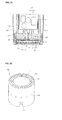
- Fig. 1 is a bottom perspective view of a lighting device 1 according to an embodiment of the present invention.
- Fig.2 is a top perspective view of the lighting device 1.
- Fig. 3 is an exploded perspective view of the lighting device 1.
- Fig. 4 is a cross sectional view of the lighting device 1.
- the lighting device 1 includes an inner case 170 of which the upper part includes a connection terminal 175 and of which the lower part includes an insertion unit 174, a heat radiating body 150 including a first receiving groove 151 into which the insertion unit 174 of the inner case 170 is inserted, a light emitting module substrate 130 emitting light onto a bottom surface of the heat radiating body 150 and including one or a plurality of light emitting devices 131, a guide member 100 being coupled to the circumference of the lower part of the heat radiating body 150 and strongly fixing the light emitting module substrate 130 to the heat radiating body 150, and an outer case 180 outside the heat radiating body 150.
- the heat radiating body 150 includes receiving grooves 151 and 152 on both sides thereof and receives the light emitting module substrate 130 and a driving unit 160.
- the heat radiating body 150 functions to radiate heat generated from the light emitting module substrate 130 or/and the driving unit 160.
- the first receiving groove 151 into which the driving unit 160 is inserted is formed on a top surface of the heat radiating body 150.
- a second receiving groove 152 into which the light emitting module substrate 130 is inserted is formed on the bottom surface of the heat radiating body 150.
- An outer surface of the heat radiating body 150 has a prominence and depression structure.
- the prominence and depression structure causes the surface area of the heat radiating body 150 to be increased, improving heat radiation efficiency.
- the heat radiating body 150 is made of a metallic material or a resin material which has excellent heat radiation efficiency.
- the material of the heat radiating body 150 may include at least one of Al, Ni, Cu, Ag, Sn and Mg.
- the light emitting module substrate 130 is disposed in the second receiving groove 152 formed on the bottom surface of the heat radiating body 150.
- the light emitting module substrate 130 includes a substrate 132 and either one or a plurality of the light emitting devices 131 disposed on the substrate 132.
- the one or each of the plurality of the light emitting devices 131 includes at least one light emitting diode (hereinafter, referred to as LED).
- the LEDs include red, green, blue and white LEDs, each of which emits red, green, blue and white lights respectively.
- the number and kind of the LED are not limited to this.
- the light emitting module substrate 130 is electrically connected to the driving unit 160 by a conductive line, etc., via a hole 153 passing through a basal surface of the heat radiating body 150. Therefore, the light emitting module substrate 130 can be driven by receiving electric power.
- a second insulation ring 155 is received in the hole 153. That is, an inner circumferential surface of the heat radiating body 150, which is formed by the hole 153, is surrounded by the second insulation ring 155. As the second insulation ring 155 is attached to the inner circumferential surface of the heat radiating body 150, it is possible to prevent moisture and impurities from penetrating between the light emitting module substrate 130 and the heat radiating body 150 and to prevent an electrical short-circuit, EMI, EMS and so on caused by contact of the conductive line with heat radiating body 150. The second insulation ring 155 can also improve a withstand voltage characteristic of the lighting device by insulating the conductive line from the heat radiating body 150.
- a heat radiating plate 140 is attached to a bottom surface of the light emitting module substrate 130.
- the heat radiating plate 140 is attached to the second receiving groove 152. Otherwise, the light emitting module substrate 130 and the heat radiating plate 140 may be also integrally formed.
- the heat radiating plate 140 allows heat generated from the light emitting module substrate 130 to be more effectively transferred to the heat radiating body 150.
- the light emitting module substrate 130 is securely fixed to the second receiving groove 152 by the guide member 100.
- the guide member 100 includes an opening 101 for exposing the one or a plurality of the light emitting devices 131 mounted on the light emitting module substrate 130.
- the guide member 100 can fix the light emitting module substrate 130 by pressing an outer circumferential surface of the light emitting module substrate 130 to the second receiving groove 152 of the heat radiating body 150.
- the guide member 100 also includes an air flow structure for allowing air to flow between the heat radiating body 150 and the outer case 180 and maximizes heat radiation efficiency of the lighting device 1.
- the air flow structure may correspond to, for example, a plurality of first heat radiating holes 102 formed between an inner surface and an outer surface of the guide member 100, or a prominence and depression structure formed on the inner surface of the guide member 100. The air flow structure will be described later in detail.
- At least one of a lens 110 and a first insulation ring 120 may be included between the guide member 100 and the light emitting module substrate 130.
- the lens 110 includes various shapes like a convex lens, a concave lens, a parabola-shaped lens and a fresnel lens, etc., so that the distribution of light emitted from the light emitting module substrate 130 can be controlled as desired.
- the lens 110 includes a fluorescent material and is used to change the wavelength of light. The lens 110 is used without being limited to this.
- the first insulation ring 120 not only prevents moisture and impurities from penetrating between the guide member 100 and the light emitting module substrate 130 but also leaves a space between an outer surface of the light emitting module substrate 130 and an inner surface of the heat radiating body 150, so that the light emitting module substrate 130 is prevented from contacting directly with the heat radiating body 150. As a result, it is possible to improve a withstand voltage characteristic of the lighting device 1 and to prevent EMI, EMS and the like of the lighting device 1.
- the inner case 170 includes the insertion unit 174 and the connection terminal 175.
- the insertion unit 174 is formed in the lower part of the inner case 170 and is inserted into the first receiving groove 151 of the heat radiating body 150.
- the connection terminal 175 is formed in the upper part of the inner case 170 and is electrically connected to an external power supply.
- a side wall of the insertion unit 174 is disposed between the driving unit 160 and the heat radiating body 150, and prevents an electrical short-circuit between them. Accordingly, it is possible to improve a withstand voltage characteristic of the lighting device 1 and to prevent EMI, EMS and the like of the lighting device 1.
- connection terminal 175 is inserted into an external power supply having a socket shape so that electric power can be supplied to the lighting device 1.
- the shape of the connection terminal 175 can be variously changed according to the design of the lighting device 1 without being limited to this.
- the driving unit 160 is disposed in the first receiving groove 151 of the heat radiating body 150.
- the driving unit 160 includes a converter converting an alternating current supplied from an external power supply into a direct current, a driving chip controlling to drive the light emitting module substrate 130, an electrostatic discharge (ESD) protective device protecting the light emitting module substrate 130.
- ESD electrostatic discharge
- the driving unit 160 is not limited to include other components.
- the outer case 180 is coupled to the inner case 170, receives the heat radiating body 150, the light emitting module substrate 130 and the driving unit 160, and forms an external appearance of the lighting device 1.
- the outer case 180 has a circular section
- the outer case 180 can be designed to have a polygon section or elliptical section and so on. There is no limit to the cross section shape of the outer case 180.
- the heat radiating body 150 is not exposed by the outer case 180, it is possible to prevent a burn accident and an electric shock and to make it easier to handle the lighting device 1.
- Fig. 5 is a perspective view of the heat radiating body 150.
- Fig.6 is a cross sectional view taken along a line A-A' of Fig. 5 .
- the first receiving groove 151 in which the driving unit 160 is disposed is formed on a first side of the heat radiating body 150.
- the second receiving groove 152 in which the light emitting module substrate 130 is disposed is formed on a second side opposite to the first side. Widths and depths of the first and the second receiving grooves 151 and 152 are changeable depending on the widths and thicknesses of the driving unit 160 and light emitting module substrate 130.
- the heat radiating body 150 is made of a metallic material or a resin material which has excellent heat radiation efficiency.
- the material of the heat radiating body 150 may include at least one of Al, Ni, Cu, Ag, Sn and Mg.
- the outer surface of the heat radiating body 150 has a prominence and depression structure.
- the prominence and depression structure causes the surface area of the heat radiating body 150 to be increased, improving heat radiation efficiency.
- the prominence and depression structure may include a wave-shaped prominence curved in one direction. However, there is no limit to the shape of the prominence and depression.
- the hole 153 is formed on the basal surface of the heat radiating body 150.
- the light emitting module substrate 130 and the driving unit 160 are electrically connected to each other by a conductive line.
- the second insulation ring 155 having a shape corresponding to that of the hole 153 is received in the hole 153. That is, the inner circumferential surface of the heat radiating body 150, which is formed by the hole 153, is surrounded by the second insulation ring 155.
- the second insulation ring 155 is attached to the inner circumferential surface of the heat radiating body 150, it is possible to prevent moisture and impurities from penetrating between the light emitting module substrate 130 and the heat radiating body 150 and to improve a withstand voltage characteristic of the lighting device by insulating the heat radiating body 150 from the conductive line passing through the hole 153.
- the second insulation ring 155 is required to have an elastic material. More specifically, the second insulation ring 155 is required to be formed of a rubber material, a silicon material or other electrical insulating material.
- Fig. 7 is a front view for describing a second insulation ring 155 and the heat radiating body 150.
- Part (a) of Fig. 8 is a front view of the second insulation ring 155 and part (b) of Fig. 8 is a bottom view of the second insulation ring 155.
- 'x' direction a direction in which the second insulation ring 155 is received in the hole 153 of the heat radiating body 150
- a step difference is formed on both an outer circumferential surface of the second insulation ring 155 and the inner circumferential surface of the heat radiating body 150, which is formed by the hole 153, respectively.
- the maximum diameter C of the second insulation ring 155 is required to be larger than the minimum diameter E of the hole 153.
- Numerical values A, A', B, C and D of the second insulation ring 155 in accordance with a TYPE of the lighting device 1 according to the present invention are shown in the following table 1.
- TYPE 1 corresponds to a 15 watt lighting device or an 8 watt lighting device.
- TYPE 2 corresponds to a 5 watt lighting device.
- a symbol “A” corresponds to a minimum diameter (or an outer diameter) of the second insulation ring 155.
- a symbol of "A' " corresponds to an inner diameter of the second insulation ring 155.
- a symbol of "B” corresponds to a height of the second insulation ring 155.
- a symbol of "C” corresponds to a maximum diameter (or an outer meter) of the second insulation ring 155.
- a symbol of "D” corresponds to a height of a part locked in the inner circumferential surface of the heat radiating body 150.
- Fig. 9 is a front view showing that the second insulation 155 ring is received in a hole 153 of the heat radiating body 150.
- the outer circumferential surface of the second insulation ring 155 is spaced apart at a predetermined interval from the inner circumferential surface of the heat radiating body 150. Accordingly, the second insulation ring 155 can be easily extracted from the hole 153 of the heat radiating body 150 at the time of working such as a change of internal parts of the lighting device.
- the predetermined interval should have a maximum value of 0.2 mm. That is, it is required that the diameter E of Fig. 7 be 0.2 mm larger than a minimum diameter A of the second insulation ring 155 and a diameter F of Fig. 7 be 0.2 mm larger than the maximum diameter C of the second insulation ring 155. If the predetermined interval is larger than 0.2 mm, the second insulation ring 155 cannot be easily extracted from the hole 153 during working. If the predetermined interval is less than 0.2 mm, the second insulation ring 155 is easily separated from the hole 153.
- Fig. 10 is a front view showing another embodiment of the second insulation ring 155.
- the second insulation ring 155 has a different shape from that of the second insulation ring 155 shown in Figs. 7 to 9 . That is, the second insulation ring 155 shown in Fig. 10 has a conical shape. The closer it is to the 'x' direction, the less the diameter of the cone-shaped second insulation ring 155 is. Since such a second insulation ring 155 cannot pass through the hole 153, it is possible to prevent the second insulation ring 155 from entering the first receiving groove 151.
- Fig. 11 is a front view showing further another embodiment of the second insulation ring 155. More specifically, Fig. 11 substitutes for an area denoted by "P" of Fig. 4 .
- the second insulation ring 155 of Fig. 11 has a different shape from that of the second insulation ring 155 of Fig. 4 . While the second insulation ring 155 shown in Fig. 4 surrounds the inner circumferential surface of the heat radiating body 150, the second insulation ring 155 shown in Fig. 11 surrounds a conductive line 165. Here, it is preferable that the second insulation ring 155 moves along the conductive line by an external force instead of being fully close and fixed to the conductive line 165.
- the second insulation ring 155 is formed to surround the conductive line 165, the conductive line 165 passing through the hole 153 is insulated from the heat radiating body 150. As a result, a withstand voltage characteristic of the lighting device 1 can be improved.
- the second insulation ring 155 is described to have a ring shape in the embodiment, any means for surrounding the conductive line and insulating the heat radiating body from the conductive line will be accepted.
- a first fastening member 154 is formed on a side of the lower part of the heat radiating body 150 in order to strongly couple the guide member 100 to the heat radiating body 150.
- the first fastening member 154 includes a hole into which a screw is inserted. The screw can strongly couple the guide member 100 to the heat radiating body 150.
- a first width P1 of the lower part of the heat radiating body 150 to which the guide member 100 is coupled is less than a second width P2 of another part of the heat radiating body 150.
- a second width P2 of another part of the heat radiating body 150 there is no limit to the widths of the heat radiating body 150.
- Fig. 12 is a perspective view showing coupling of the light emitting module substrate 130 and the first insulation ring 120.
- Fig. 13 is a cross sectional view taken along a line B-B' of Fig. 12 .
- the light emitting module substrate 130 is disposed in the second receiving groove 152.
- the first insulation ring 120 is coupled to the circumference of the light emitting module substrate 130.
- the light emitting module substrate 130 includes the substrate 132 and one or a plurality of the plurality of the light emitting devices 131 mounted on the substrate 132.
- the substrate 132 is made by printing a circuit pattern on an insulator.
- a common printed circuit board (PCB), a metal core PCB, a flexible PCB and a ceramic PCB and the like can be used as the substrate 132.
- the substrate 132 is made of a material capable of efficiently reflecting light. White and silver colors, etc., capable of efficiently reflecting light is formed on the surface of the substrate 132.
- the one or a plurality of the light emitting devices 131 are mounted on the substrate 132.
- Each of a plurality of the light emitting devices 131 includes at least one light emitting diode (LED).
- the LEDs include various colors such as red, green, blue and white, each of which emits red, green, blue and white lights respectively. The number and kind of the LED are not limited to this.
- the light emitting device is not necessarily mounted on either an area of the light emitting module substrate 130, which corresponds to an area in which the conductive line has been formed or an area of the substrate 132, which corresponds to an area facing the hole 153.
- the conductive line is formed in the middle area of the light emitting module substrate 130, the light emitting device is not necessarily mounted on the middle area.
- the heat radiating plate 140 is attached to the lower surface of the light emitting module substrate 130.
- the heat radiating plate 140 is made of a material having a high thermal conductivity such as a thermal conduction silicon pad or a thermal conduction tape and the like.
- the heat radiating plate 140 can effectively transfer heat generated by the light emitting module substrate 130 to the heat radiating body 150.
- the first insulation ring 120 is formed of a rubber material, a silicon material or other electrical insulating material.
- the first insulation ring 120 is formed in the circumference of the light emitting module substrate 130. More specifically, as shown, the first insulation ring 120 includes a step difference 121 in an inner lower end thereof. The lateral surface of the light emitting module substrate 130 and the circumference of the top surface of the light emitting module substrate 130 come in contact with the step difference 121 of the inner lower end of the first insulation ring 120. An area contacting with the step difference 121 is not limited to this. Additionally, an inner upper end of the first insulation ring 120 may includes an inclination 122 in order to improve the light distribution of the light emitting module substrate 130.
- the first insulation ring 120 not only prevents moisture and impurities from penetrating between the guide member 100 and the light emitting module substrate 130 but also prevents the lateral surface of the light emitting module substrate 130 from directly contacting with the heat radiating body 150. As a result, it is possible to improve a withstand voltage characteristic of the lighting device 1 and to prevent EMI, EMS and the like of the lighting device 1.
- the first insulation ring 120 strongly fixes and protects the light emitting module substrate 130, improving the reliability of the lighting device 1.
- the first insulation ring 120 allows the lens 110 to be disposed apart from the light emitting module substrate 130 by a first distance "h". As a result, it is much easier to control the light distribution of the lighting device 1.
- Fig. 14 is a perspective view of a guide member 100.
- Fig. 15 is a plan view of the guide member of Fig. 14 .
- the guide member 100 includes an opening 101 for exposing the light emitting module substrate 130, a plurality of heat radiating holes 102 between the inside and the outside of the guide member 100, and a locking groove 103 coupled to the heat radiating body 150.
- the guide member 100 is shown in the form of a circular ring, the guide member 100 can have also shapes such as a polygon and an elliptical ring. There is no limit to the shape of the guide member 100.
- the one or a plurality of the light emitting devices 131 of the light emitting module substrate 130 are exposed through the opening 101. Since the guide member 100 presses the light emitting module substrate 130 to the second receiving groove 152, the width of the opening 101 is required to be less than that of the light emitting module substrate 130.
- the guide member 100 As the guide member 100 is coupled to the heat radiating body 150, the guide member 100 give a pressure to the lens 110, the first insulation ring 120 and the circumference of the light emitting module substrate 130. Accordingly, the lens 110, the first insulation ring 120 and the light emitting module substrate 130 can be securely fixed to the second receiving groove 152 of the heat radiating body 150, thereby improving the reliability of the lighting device 1.
- the guide member 100 can be coupled to the heat radiating body 150 through the locking groove 103.
- a hole of the first fastening member 154 of the heat radiating body 150 is in a line with the locking groove 103 of the guide member 100. Then, the guide member 100 is coupled to the heat radiating body 150 by inserting a screw into the hole of the first fastening member 154 and the locking groove 103.
- the guide member 100 is easily separated from the heat radiating body 150. Therefore, users can perform maintenance for the lighting device 1 without difficulty.
- the plurality of the first heat radiating holes 102 are formed between the inside of the outside of the guide member 100.
- the plurality of the first heat radiating holes 102 allows air inside the lighting device 1 to smoothly flow, thereby maximizing heat radiation efficiency.
- a description thereof will be provided.
- Fig. 16 is a cross sectional view showing an enlarged lower part of the lighting device 1 according to the embodiment.
- Fig. 17 is a bottom view of the lighting device 1.
- Fig. 18 is a top view of the lighting device 1.
- air flowing into the inside of the lighting device 1 through the plurality of the first heat radiating holes 102 flows to a prominence "a" and depression “b" of the lateral surface of the heat radiating body 150.
- the air heated by passing through the prominence and depression structure of the heat radiating body 150 can flow out through a plurality of ventilating holes 182 formed between the inner case 170 and the outer case 180. Otherwise, air flown into the plurality of the ventilating holes 182 may flow out through the plurality of the first heat radiating holes 102. Air can flow out in various ways without being limited to this.
- a guide member 100A has a prominence and depression structure in the inner surface thereof, so that air can flow into the inside of the lighting device through a depression 102A.
- the lens 110 is formed under the light emitting module substrate 130 and controls the distribution of light emitted from the light emitting module substrate 130.
- the lens 110 has various shapes.
- the lens 110 includes at least one of a parabola-shaped lens, a fresnel lens, a convex lens or a concave lens.
- the lens 110 is disposed under the light emitting module substrate 130 and spaced apart from the light emitting module substrate 130 by a first distance "h".
- the first distance "h" is greater than 0 mm and equal to or less than 50 mm in accordance with the design of the lighting device 1.
- the distance “h” is maintained by the first insulation ring 120 disposed between the light emitting module substrate 130 and the lens 110. Otherwise, if another support for supporting the lens 110 is provided in the second receiving groove 152 of the heat radiating body 150, the distance “h” is maintained between the light emitting module substrate 130 and the lens 110. There is no limit to the method for maintaining the distance "h”.
- the lens 110 is fixed by the guide member 110.
- the inner surface of the guide member 100 contacts with the lens 110.
- the lens 110 and the light emitting module substrate 130 are pressed and fixed to the second receiving groove 152 of the heat radiating body 150 by the inner surface of the guide member 100.
- the lens 110 is made of glass, polymethylmethacrylate (PMMA) and polycarbornate (PC) and so on.
- the lens 110 includes fluorescent material. Otherwise, a photo luminescent film (PLF) including the fluorescent material is attached to a light incident surface or a light emitting surface of the lens 110. Light emitted from the light emitting module substrate 130 by the fluorescent material is emitted with a varied wavelength.
- PPF photo luminescent film
- Fig. 20 is a perspective view of the inner case 170 of the lighting device 1 of Fig. 1 .
- the inner case 170 includes an insertion unit 174 inserted into the first receiving groove 151 of the heat radiating body 150, a connection terminal 175 electrically connected to an external power supply, and a second fastening member 172 coupled to the outer case 180.
- the inner case 170 is made of a material with excellent insulating properties and endurance, for example, a resin material.
- the insertion unit 174 is formed in the lower part of the inner case 170. A side wall of the insertion unit 174 is inserted into the first receiving groove 151 so that an electrical short-circuit between the driving unit 160 and the heat radiating body 150. As a result, a withstand voltage of the lighting device 1 can be improved.
- connection terminal 175 is, for example, connected to an external power supply in the form of a socket. That is, the connection terminal 175 includes a first electrode 177 at the top thereof, a second electrode 178 on the lateral surface thereof, and an insulating member 179 between the first electrode 177 and the second electrode 178.
- the first and second electrodes 177 and 178 are supplied with electric power by an external power supply.
- shape of the terminal 175 is variously changed based on the design of the lighting device 1, there is no limit to the shape of the terminal 175.
- the second fastening member 172 is formed on the lateral surface of the inner case 170 and includes a plurality of holes.
- the inner case 170 is coupled to the outer case 180 by inserting screws and the like into the plurality of the holes.
- a plurality of second heat radiating holes 176 are formed in the inner case 170, improving the heat radiation efficiency of the inside of the inner case 170.
- the driving unit 160 is disposed in the first receiving groove 151 of the heat radiating body 150.
- the driving unit 160 includes a supporting substrate 161 and a plurality of parts 162 mounted on the supporting substrate 161.
- a plurality of the parts 162 include, for example, a converter converting an alternating current supplied from an external power supply into a direct current, a driving chip controlling to drive the light emitting module substrate 130, an electrostatic discharge (ESD) protective device protecting the light emitting module substrate 130.
- ESD electrostatic discharge
- the driving unit 160 is not limited to include other components.
- the supporting substrate 161 is disposed vertically in order that air flows smoothly in the inner case 170. Therefore, as compared with a case where the supporting substrate 161 is disposed horizontally, air flows up and down in the inner case 170 due to air convection, thereby improving the heat radiation efficiency of the lighting device 1.
- the supporting substrate 161 may be disposed horizontally in the inner case 170.
- the supporting substrate 161 can be disposed in various ways without being limited to this.
- the driving unit 160 is electrically connected to the connection terminal 175 of the inner case 170 by a first conductive line 164 and to the light emitting module substrate 130 by a second conductive line 165.
- the first conductive line 164 is connected to the first electrode 177 and the second electrode 178 of the connection terminal 175 so that electric power is supplied from an external power supply.
- the second conductive line 165 passes through the hole 153 of the heat radiating body 150 and electrically connects the driving unit 160 with the light emitting module substrate 130.
- the supporting substrate 161 is disposed vertically in the inner case 170. Therefore, a long-term use of the lighting device 1 causes the supporting substrate 161 to press and damage the second conductive line 165.
- a projection 159 is formed on the basal surface of the light emitting module substrate 130 in the vicinity of the hole 153, so that it is possible not only to support the supporting substrate 161 but to prevent in advance the second conductive line 165 from being damaged.
- the outer case 180 is coupled to the inner case 170, receives the heat radiating body 150, the light emitting module substrate 130 and the driving unit 160, etc., and forms an external shape of the lighting device 1.
- the outer case 180 surrounds the heat radiating body 150, a burn accident and an electric shock can be prevented and a user can manage the lighting device 1 with ease.
- the outer case 180 will be described in detail.
- Fig. 22 is a perspective view of an outer case 180.
- the outer case 180 includes an opening 181 into which the inner case 170 and the like are inserted, a coupling groove 183 coupled to the second fastening member 172 of the inner case 170, and a plurality of ventilating holes 182 for allowing air to flow into the lighting device or to flow to the outside of the lighting device.
- the outer case 180 is made of a material with excellent insulation and endurance, for example, a resin material.
- the inner case 170 is inserted into the opening 181 of the outer case 180.
- the second fastening member 172 of the inner case 170 is coupled to the coupling groove 183 by means of a screw and the like. As a result, the outer case 180 and the inner case 170 are coupled to each other.
- the plurality of the ventilating holes 182 as well as the plurality of the first heat radiating holes 102 of the guide member 100 allow air to smoothly flow in the lighting device 1, thereby improving the heat radiation efficiency of the lighting device 1.
- the plurality of the ventilating holes 182 are formed in the circumference of the top surface of the outer case 180.
- the ventilating hole 182 has an arc-shape like a fan.
- the coupling groove 183 is formed between the plurality of the ventilating holes 182.
- the lateral surface of the outer case 180 may include at least a marking groove 185 and a plurality of holes 184.
- the hole 184 is used to enhance heat radiation efficiency.
- the marking groove 185 is used to easily managing the lighting device 1. However, it is not necessary to form the plurality of holes 184 and the marking groove 185. There is no limit to the formation of the hole 184 and the marking hole 185.
Abstract
a substrate (132);
a light emitting device (131) disposed on the substrate;
a driving unit (160) supplying electric power to the light emitting device and connected to the substrate through a conductive line;
a heat radiating body (150) radiating heat from the light emitting devices and comprising a hole (153) through which the conductive line to pass; and
an insulator (120,155) coupled with the hole and having an opening.
Description
- The present application claims priority under 35 U.S.C. § 119(e) of Korean Patent Applications Nos.
10-2009-0107498 filed on November 9, 2009 10-2010-0032060 filed on April 7, 2010 - This embodiment relates to a lighting device.
- A light emitting diode (LED) is a semiconductor element for converting electric energy into light. The LED has advantages of low power consumption, a semi-permanent span of life, a rapid response speed, safety and an environment-friendliness. Therefore, many researches are devoted to substitution of the existing light sources with the LED. The LED is now being increasingly used as a light source for lighting devices, for example, various lamps used interiorly and exteriorly, a liquid crystal display device, an electric sign and a street lamp and the like.
- One embodiment is a lighting device. The lighting device includes:
- a substrate;
- a light emitting device disposed on the substrate;
- a driving unit supplying electric power to the light emitting device and connected to the substrate through a conductive line;
- a heat radiating body radiating heat from the light emitting devices and comprising a hole through which the conductive line to pass; and
- an insulator coupled with the hole and having a opening.
-
-
Fig. 1 is a bottom perspective view of a lighting device according to an embodiment of the present invention. -
Fig.2 is a top perspective view of the lighting device ofFig. 1 . -
Fig. 3 is an exploded perspective view of the lighting device ofFig. 1 . -
Fig. 4 is a cross sectional view of the lighting device ofFig. 1 . -
Fig. 5 is a perspective view of a heat radiating body of the lighting device ofFig. 1 . -
Fig.6 is a cross sectional view taken along a line A-A' ofFig. 5 . -
Fig. 7 is a front view for describing a second insulation ring and the heat radiating body. - Part (a) of
Fig. 8 is a front view of the second insulation ring and part (b) ofFig. 8 is a bottom view of the second insulation ring. -
Fig. 9 is a front view showing that the second insulation ring is received in a hole of the heat radiating body. -
Fig. 10 is a front view showing another embodiment of the second insulation ring. -
Fig. 11 is a front view showing further another embodiment of the second insulation ring. -
Fig. 12 is a perspective view showing coupling of a light emitting module substrate and a first insulation ring of the lighting device ofFig. 1 . -
Fig. 13 is a cross sectional view taken along a line B-B' ofFig. 12 . -
Fig. 14 is a perspective view of a guide member of the lighting device ofFig. 1 . -
Fig. 15 is a plan view of the guide member ofFig. 14 . -
Fig. 16 is a cross sectional view showing an enlarged lower part of the lighting device of -
Fig. 1 . -
Fig. 17 is a bottom view of the lighting device ofFig. 1 . -
Fig. 18 is a top view of the lighting device ofFig. 1 . -
Fig. 19 is a perspective view of a guide member of a lighting device according to another embodiment. -
Fig. 20 is a perspective view of an inner case of the lighting device ofFig. 1 . -
Fig. 21 is a view showing a heat radiating body of the lighting device according to the another embodiment. -
Fig. 22 is a perspective view of an outer case of the lighting device ofFig. 1 . - Hereinafter, an embodiment will be described in detail with reference to the accompanying drawings.
- It will be understood that when an element is referred to as being 'on' or "under" another element, it can be directly on/under the element, and one or more intervening elements may also be present.
-
Fig. 1 is a bottom perspective view of alighting device 1 according to an embodiment of the present invention.Fig.2 is a top perspective view of thelighting device 1.Fig. 3 is an exploded perspective view of thelighting device 1.Fig. 4 is a cross sectional view of thelighting device 1. - Referring to
Figs. 1 to 4 , thelighting device 1 includes aninner case 170 of which the upper part includes aconnection terminal 175 and of which the lower part includes aninsertion unit 174, aheat radiating body 150 including a first receivinggroove 151 into which theinsertion unit 174 of theinner case 170 is inserted, a lightemitting module substrate 130 emitting light onto a bottom surface of theheat radiating body 150 and including one or a plurality oflight emitting devices 131, aguide member 100 being coupled to the circumference of the lower part of theheat radiating body 150 and strongly fixing the lightemitting module substrate 130 to theheat radiating body 150, and anouter case 180 outside theheat radiating body 150. - The
heat radiating body 150 includes receivinggrooves emitting module substrate 130 and adriving unit 160. Theheat radiating body 150 functions to radiate heat generated from the lightemitting module substrate 130 or/and thedriving unit 160. - Specifically, as shown in
Figs. 3 and4 , the first receivinggroove 151 into which thedriving unit 160 is inserted is formed on a top surface of theheat radiating body 150. A second receivinggroove 152 into which the lightemitting module substrate 130 is inserted is formed on the bottom surface of theheat radiating body 150. - An outer surface of the
heat radiating body 150 has a prominence and depression structure. The prominence and depression structure causes the surface area of theheat radiating body 150 to be increased, improving heat radiation efficiency. Theheat radiating body 150 is made of a metallic material or a resin material which has excellent heat radiation efficiency. However, there is no limit to the material of theheat radiating body 150. For example, the material of theheat radiating body 150 may include at least one of Al, Ni, Cu, Ag, Sn and Mg. - The light
emitting module substrate 130 is disposed in the second receivinggroove 152 formed on the bottom surface of theheat radiating body 150. The lightemitting module substrate 130 includes asubstrate 132 and either one or a plurality of thelight emitting devices 131 disposed on thesubstrate 132. - The one or each of the plurality of the
light emitting devices 131 includes at least one light emitting diode (hereinafter, referred to as LED). The LEDs include red, green, blue and white LEDs, each of which emits red, green, blue and white lights respectively. The number and kind of the LED are not limited to this. - The light
emitting module substrate 130 is electrically connected to thedriving unit 160 by a conductive line, etc., via ahole 153 passing through a basal surface of theheat radiating body 150. Therefore, the lightemitting module substrate 130 can be driven by receiving electric power. - Here, a
second insulation ring 155 is received in thehole 153. That is, an inner circumferential surface of theheat radiating body 150, which is formed by thehole 153, is surrounded by thesecond insulation ring 155. As thesecond insulation ring 155 is attached to the inner circumferential surface of theheat radiating body 150, it is possible to prevent moisture and impurities from penetrating between the light emittingmodule substrate 130 and theheat radiating body 150 and to prevent an electrical short-circuit, EMI, EMS and so on caused by contact of the conductive line withheat radiating body 150. Thesecond insulation ring 155 can also improve a withstand voltage characteristic of the lighting device by insulating the conductive line from theheat radiating body 150. - A
heat radiating plate 140 is attached to a bottom surface of the light emittingmodule substrate 130. Theheat radiating plate 140 is attached to thesecond receiving groove 152. Otherwise, the light emittingmodule substrate 130 and theheat radiating plate 140 may be also integrally formed. Theheat radiating plate 140 allows heat generated from the light emittingmodule substrate 130 to be more effectively transferred to theheat radiating body 150. - The light emitting
module substrate 130 is securely fixed to thesecond receiving groove 152 by theguide member 100. Theguide member 100 includes anopening 101 for exposing the one or a plurality of thelight emitting devices 131 mounted on the light emittingmodule substrate 130. Theguide member 100 can fix the light emittingmodule substrate 130 by pressing an outer circumferential surface of the light emittingmodule substrate 130 to thesecond receiving groove 152 of theheat radiating body 150. - The
guide member 100 also includes an air flow structure for allowing air to flow between theheat radiating body 150 and theouter case 180 and maximizes heat radiation efficiency of thelighting device 1. The air flow structure may correspond to, for example, a plurality of firstheat radiating holes 102 formed between an inner surface and an outer surface of theguide member 100, or a prominence and depression structure formed on the inner surface of theguide member 100. The air flow structure will be described later in detail. - At least one of a
lens 110 and afirst insulation ring 120 may be included between theguide member 100 and the light emittingmodule substrate 130. - The
lens 110 includes various shapes like a convex lens, a concave lens, a parabola-shaped lens and a fresnel lens, etc., so that the distribution of light emitted from the light emittingmodule substrate 130 can be controlled as desired. Thelens 110 includes a fluorescent material and is used to change the wavelength of light. Thelens 110 is used without being limited to this. - The
first insulation ring 120 not only prevents moisture and impurities from penetrating between theguide member 100 and the light emittingmodule substrate 130 but also leaves a space between an outer surface of the light emittingmodule substrate 130 and an inner surface of theheat radiating body 150, so that the light emittingmodule substrate 130 is prevented from contacting directly with theheat radiating body 150. As a result, it is possible to improve a withstand voltage characteristic of thelighting device 1 and to prevent EMI, EMS and the like of thelighting device 1. - As shown in
Figs. 3 and4 , theinner case 170 includes theinsertion unit 174 and theconnection terminal 175. Theinsertion unit 174 is formed in the lower part of theinner case 170 and is inserted into thefirst receiving groove 151 of theheat radiating body 150. Theconnection terminal 175 is formed in the upper part of theinner case 170 and is electrically connected to an external power supply. - A side wall of the
insertion unit 174 is disposed between the drivingunit 160 and theheat radiating body 150, and prevents an electrical short-circuit between them. Accordingly, it is possible to improve a withstand voltage characteristic of thelighting device 1 and to prevent EMI, EMS and the like of thelighting device 1. - The
connection terminal 175 is inserted into an external power supply having a socket shape so that electric power can be supplied to thelighting device 1. However, the shape of theconnection terminal 175 can be variously changed according to the design of thelighting device 1 without being limited to this. - The driving
unit 160 is disposed in thefirst receiving groove 151 of theheat radiating body 150. The drivingunit 160 includes a converter converting an alternating current supplied from an external power supply into a direct current, a driving chip controlling to drive the light emittingmodule substrate 130, an electrostatic discharge (ESD) protective device protecting the light emittingmodule substrate 130. The drivingunit 160 is not limited to include other components. - The
outer case 180 is coupled to theinner case 170, receives theheat radiating body 150, the light emittingmodule substrate 130 and thedriving unit 160, and forms an external appearance of thelighting device 1. - While the
outer case 180 has a circular section, theouter case 180 can be designed to have a polygon section or elliptical section and so on. There is no limit to the cross section shape of theouter case 180. - Since the
heat radiating body 150 is not exposed by theouter case 180, it is possible to prevent a burn accident and an electric shock and to make it easier to handle thelighting device 1. - Hereinafter, the following detailed description will be focused on each component of the
lighting device 1 according to the embodiment. -
Fig. 5 is a perspective view of theheat radiating body 150.Fig.6 is a cross sectional view taken along a line A-A' ofFig. 5 . - Referring to
Figs. 4 to 6 , thefirst receiving groove 151 in which thedriving unit 160 is disposed is formed on a first side of theheat radiating body 150. Thesecond receiving groove 152 in which the light emittingmodule substrate 130 is disposed is formed on a second side opposite to the first side. Widths and depths of the first and the second receivinggrooves driving unit 160 and light emittingmodule substrate 130. - The
heat radiating body 150 is made of a metallic material or a resin material which has excellent heat radiation efficiency. However, there is no limit to the material of theheat radiating body 150. For example, For example, the material of theheat radiating body 150 may include at least one of Al, Ni, Cu, Ag, Sn and Mg. - The outer surface of the
heat radiating body 150 has a prominence and depression structure. The prominence and depression structure causes the surface area of theheat radiating body 150 to be increased, improving heat radiation efficiency. As shown, the prominence and depression structure may include a wave-shaped prominence curved in one direction. However, there is no limit to the shape of the prominence and depression. - The
hole 153 is formed on the basal surface of theheat radiating body 150. The light emittingmodule substrate 130 and thedriving unit 160 are electrically connected to each other by a conductive line. - Here, the
second insulation ring 155 having a shape corresponding to that of thehole 153 is received in thehole 153. That is, the inner circumferential surface of theheat radiating body 150, which is formed by thehole 153, is surrounded by thesecond insulation ring 155. - As the
second insulation ring 155 is attached to the inner circumferential surface of theheat radiating body 150, it is possible to prevent moisture and impurities from penetrating between the light emittingmodule substrate 130 and theheat radiating body 150 and to improve a withstand voltage characteristic of the lighting device by insulating theheat radiating body 150 from the conductive line passing through thehole 153. Here, thesecond insulation ring 155 is required to have an elastic material. More specifically, thesecond insulation ring 155 is required to be formed of a rubber material, a silicon material or other electrical insulating material. -
Fig. 7 is a front view for describing asecond insulation ring 155 and theheat radiating body 150. Part (a) ofFig. 8 is a front view of thesecond insulation ring 155 and part (b) ofFig. 8 is a bottom view of thesecond insulation ring 155. - First, referring to
Fig. 7 , the closer it is to a direction in which thesecond insulation ring 155 is received in thehole 153 of the heat radiating body 150 (hereinafter, referred to as 'x' direction), the less the diameter of thesecond insulation ring 155 is. The closer it is to the 'x' direction, the less the diameter of thehole 153 is. For a concrete example, referring to (a) to (b) ofFig. 8 , a step difference is formed on both an outer circumferential surface of thesecond insulation ring 155 and the inner circumferential surface of theheat radiating body 150, which is formed by thehole 153, respectively. Here, in order that thesecond insulation ring 155 is received and fixed in thehole 153, the maximum diameter C of thesecond insulation ring 155 is required to be larger than the minimum diameter E of thehole 153. - As such, when a step difference is formed on both the outer circumferential surface of the
second insulation ring 155 and the inner circumferential surface of theheat radiating body 150, and when the maximum diameter C of thesecond insulation ring 155 is larger than the minimum diameter E of thehole 153, thesecond insulation ring 155 cannot pass through thehole 153. As a result, it is possible to prevent thesecond insulation ring 155 from entering thefirst receiving groove 151. - Numerical values A, A', B, C and D of the
second insulation ring 155 in accordance with a TYPE of thelighting device 1 according to the present invention are shown in the following table 1. Here,TYPE 1 corresponds to a 15 watt lighting device or an 8 watt lighting device. TYPE 2 corresponds to a 5 watt lighting device. A symbol "A" corresponds to a minimum diameter (or an outer diameter) of thesecond insulation ring 155. A symbol of "A' " corresponds to an inner diameter of thesecond insulation ring 155. A symbol of "B" corresponds to a height of thesecond insulation ring 155. A symbol of "C" corresponds to a maximum diameter (or an outer meter) of thesecond insulation ring 155. A symbol of "D" corresponds to a height of a part locked in the inner circumferential surface of theheat radiating body 150.
-
Fig. 9 is a front view showing that thesecond insulation 155 ring is received in ahole 153 of theheat radiating body 150. - As shown in
Fig. 9 , the outer circumferential surface of thesecond insulation ring 155 is spaced apart at a predetermined interval from the inner circumferential surface of theheat radiating body 150. Accordingly, thesecond insulation ring 155 can be easily extracted from thehole 153 of theheat radiating body 150 at the time of working such as a change of internal parts of the lighting device. - Here, it is required that the predetermined interval should have a maximum value of 0.2 mm. That is, it is required that the diameter E of
Fig. 7 be 0.2 mm larger than a minimum diameter A of thesecond insulation ring 155 and a diameter F ofFig. 7 be 0.2 mm larger than the maximum diameter C of thesecond insulation ring 155. If the predetermined interval is larger than 0.2 mm, thesecond insulation ring 155 cannot be easily extracted from thehole 153 during working. If the predetermined interval is less than 0.2 mm, thesecond insulation ring 155 is easily separated from thehole 153. -
Fig. 10 is a front view showing another embodiment of thesecond insulation ring 155. - Referring to
Fig. 10 , thesecond insulation ring 155 has a different shape from that of thesecond insulation ring 155 shown inFigs. 7 to 9 . That is, thesecond insulation ring 155 shown inFig. 10 has a conical shape. The closer it is to the 'x' direction, the less the diameter of the cone-shapedsecond insulation ring 155 is. Since such asecond insulation ring 155 cannot pass through thehole 153, it is possible to prevent thesecond insulation ring 155 from entering thefirst receiving groove 151. -
Fig. 11 is a front view showing further another embodiment of thesecond insulation ring 155. More specifically,Fig. 11 substitutes for an area denoted by "P" ofFig. 4 . - Referring to
Fig. 11 , thesecond insulation ring 155 ofFig. 11 has a different shape from that of thesecond insulation ring 155 ofFig. 4 . While thesecond insulation ring 155 shown inFig. 4 surrounds the inner circumferential surface of theheat radiating body 150, thesecond insulation ring 155 shown inFig. 11 surrounds aconductive line 165. Here, it is preferable that thesecond insulation ring 155 moves along the conductive line by an external force instead of being fully close and fixed to theconductive line 165. - Since the
second insulation ring 155 is formed to surround theconductive line 165, theconductive line 165 passing through thehole 153 is insulated from theheat radiating body 150. As a result, a withstand voltage characteristic of thelighting device 1 can be improved. - As such, though the
second insulation ring 155 is described to have a ring shape in the embodiment, any means for surrounding the conductive line and insulating the heat radiating body from the conductive line will be accepted. - A
first fastening member 154 is formed on a side of the lower part of theheat radiating body 150 in order to strongly couple theguide member 100 to theheat radiating body 150. Thefirst fastening member 154 includes a hole into which a screw is inserted. The screw can strongly couple theguide member 100 to theheat radiating body 150. - In addition, so as to easily couple the
guide member 100, a first width P1 of the lower part of theheat radiating body 150 to which theguide member 100 is coupled is less than a second width P2 of another part of theheat radiating body 150. However, there is no limit to the widths of theheat radiating body 150. -
Fig. 12 is a perspective view showing coupling of the light emittingmodule substrate 130 and thefirst insulation ring 120.Fig. 13 is a cross sectional view taken along a line B-B' ofFig. 12 . - Referring to
Figs. 3 ,12 and 13 , the light emittingmodule substrate 130 is disposed in thesecond receiving groove 152. Thefirst insulation ring 120 is coupled to the circumference of the light emittingmodule substrate 130. - The light emitting
module substrate 130 includes thesubstrate 132 and one or a plurality of the plurality of thelight emitting devices 131 mounted on thesubstrate 132. - The
substrate 132 is made by printing a circuit pattern on an insulator. For example, a common printed circuit board (PCB), a metal core PCB, a flexible PCB and a ceramic PCB and the like can be used as thesubstrate 132. - The
substrate 132 is made of a material capable of efficiently reflecting light. White and silver colors, etc., capable of efficiently reflecting light is formed on the surface of thesubstrate 132. - The one or a plurality of the
light emitting devices 131 are mounted on thesubstrate 132. Each of a plurality of thelight emitting devices 131 includes at least one light emitting diode (LED). The LEDs include various colors such as red, green, blue and white, each of which emits red, green, blue and white lights respectively. The number and kind of the LED are not limited to this. - Meanwhile, there is no limit in disposing one or more light emitting
devices 131. However, in the embodiment, while the conductive line is formed under the light emittingmodule substrate 130, the light emitting device is not necessarily mounted on either an area of the light emittingmodule substrate 130, which corresponds to an area in which the conductive line has been formed or an area of thesubstrate 132, which corresponds to an area facing thehole 153. For example, as shown, when the conductive line is formed in the middle area of the light emittingmodule substrate 130, the light emitting device is not necessarily mounted on the middle area. - The
heat radiating plate 140 is attached to the lower surface of the light emittingmodule substrate 130. Theheat radiating plate 140 is made of a material having a high thermal conductivity such as a thermal conduction silicon pad or a thermal conduction tape and the like. Theheat radiating plate 140 can effectively transfer heat generated by the light emittingmodule substrate 130 to theheat radiating body 150. - The
first insulation ring 120 is formed of a rubber material, a silicon material or other electrical insulating material. Thefirst insulation ring 120 is formed in the circumference of the light emittingmodule substrate 130. More specifically, as shown, thefirst insulation ring 120 includes astep difference 121 in an inner lower end thereof. The lateral surface of the light emittingmodule substrate 130 and the circumference of the top surface of the light emittingmodule substrate 130 come in contact with thestep difference 121 of the inner lower end of thefirst insulation ring 120. An area contacting with thestep difference 121 is not limited to this. Additionally, an inner upper end of thefirst insulation ring 120 may includes aninclination 122 in order to improve the light distribution of the light emittingmodule substrate 130. - The
first insulation ring 120 not only prevents moisture and impurities from penetrating between theguide member 100 and the light emittingmodule substrate 130 but also prevents the lateral surface of the light emittingmodule substrate 130 from directly contacting with theheat radiating body 150. As a result, it is possible to improve a withstand voltage characteristic of thelighting device 1 and to prevent EMI, EMS and the like of thelighting device 1. - The
first insulation ring 120 strongly fixes and protects the light emittingmodule substrate 130, improving the reliability of thelighting device 1. - Referring to
Fig. 16 , when thelens 110 is disposed on thefirst insulation ring 120, thefirst insulation ring 120 allows thelens 110 to be disposed apart from the light emittingmodule substrate 130 by a first distance "h". As a result, it is much easier to control the light distribution of thelighting device 1. -
Fig. 14 is a perspective view of aguide member 100.Fig. 15 is a plan view of the guide member ofFig. 14 . - Referring to
Figs. 4 ,14 and15 , theguide member 100 includes anopening 101 for exposing the light emittingmodule substrate 130, a plurality ofheat radiating holes 102 between the inside and the outside of theguide member 100, and a lockinggroove 103 coupled to theheat radiating body 150. - While the
guide member 100 is shown in the form of a circular ring, theguide member 100 can have also shapes such as a polygon and an elliptical ring. There is no limit to the shape of theguide member 100. - The one or a plurality of the
light emitting devices 131 of the light emittingmodule substrate 130 are exposed through theopening 101. Since theguide member 100 presses the light emittingmodule substrate 130 to thesecond receiving groove 152, the width of theopening 101 is required to be less than that of the light emittingmodule substrate 130. - More specifically, as the
guide member 100 is coupled to theheat radiating body 150, theguide member 100 give a pressure to thelens 110, thefirst insulation ring 120 and the circumference of the light emittingmodule substrate 130. Accordingly, thelens 110, thefirst insulation ring 120 and the light emittingmodule substrate 130 can be securely fixed to thesecond receiving groove 152 of theheat radiating body 150, thereby improving the reliability of thelighting device 1. - The
guide member 100 can be coupled to theheat radiating body 150 through the lockinggroove 103. For example, as shown inFigs. 4 , a hole of thefirst fastening member 154 of theheat radiating body 150 is in a line with the lockinggroove 103 of theguide member 100. Then, theguide member 100 is coupled to theheat radiating body 150 by inserting a screw into the hole of thefirst fastening member 154 and the lockinggroove 103. However, there is no limit to the method for coupling theguide member 100 to theheat radiating body 150. - Meanwhile, when internal parts such as the driving
unit 160 and the light emittingmodule substrate 130 and the like of thelighting device 1 are required to be changed, theguide member 100 is easily separated from theheat radiating body 150. Therefore, users can perform maintenance for thelighting device 1 without difficulty. - The plurality of the first
heat radiating holes 102 are formed between the inside of the outside of theguide member 100. The plurality of the firstheat radiating holes 102 allows air inside thelighting device 1 to smoothly flow, thereby maximizing heat radiation efficiency. Hereinafter, a description thereof will be provided. -
Fig. 16 is a cross sectional view showing an enlarged lower part of thelighting device 1 according to the embodiment.Fig. 17 is a bottom view of thelighting device 1.Fig. 18 is a top view of thelighting device 1. - Referring to
Figs. 16 to 18 , air flowing into the inside of thelighting device 1 through the plurality of the firstheat radiating holes 102 flows to a prominence "a" and depression "b" of the lateral surface of theheat radiating body 150. Based on a principle of air convection, the air heated by passing through the prominence and depression structure of theheat radiating body 150 can flow out through a plurality of ventilatingholes 182 formed between theinner case 170 and theouter case 180. Otherwise, air flown into the plurality of the ventilating holes 182 may flow out through the plurality of the first heat radiating holes 102. Air can flow out in various ways without being limited to this. - In other words, it is possible to radiate heat by using the principle of air convection through the plurality of the first
heat radiating holes 102 and the plurality of the ventilating holes 182, thereby maximizing heat radiation efficiency. Hereinafter, a description thereof will be provided. - Meanwhile, the air flow structure of the
guide member 100 is not limited to this and can be changed variously. For example, as shown inFig. 19 , aguide member 100A according to another embodiment has a prominence and depression structure in the inner surface thereof, so that air can flow into the inside of the lighting device through adepression 102A. - Referring to
Figs. 4 and16 , thelens 110 is formed under the light emittingmodule substrate 130 and controls the distribution of light emitted from the light emittingmodule substrate 130. - The
lens 110 has various shapes. For example, thelens 110 includes at least one of a parabola-shaped lens, a fresnel lens, a convex lens or a concave lens. - The
lens 110 is disposed under the light emittingmodule substrate 130 and spaced apart from the light emittingmodule substrate 130 by a first distance "h". The first distance "h" is greater than 0 mm and equal to or less than 50 mm in accordance with the design of thelighting device 1. - The distance "h" is maintained by the
first insulation ring 120 disposed between the light emittingmodule substrate 130 and thelens 110. Otherwise, if another support for supporting thelens 110 is provided in thesecond receiving groove 152 of theheat radiating body 150, the distance "h" is maintained between the light emittingmodule substrate 130 and thelens 110. There is no limit to the method for maintaining the distance "h". - The
lens 110 is fixed by theguide member 110. The inner surface of theguide member 100 contacts with thelens 110. Thelens 110 and the light emittingmodule substrate 130 are pressed and fixed to thesecond receiving groove 152 of theheat radiating body 150 by the inner surface of theguide member 100. - The
lens 110 is made of glass, polymethylmethacrylate (PMMA) and polycarbornate (PC) and so on. - According to the design of the
lighting device 1, thelens 110 includes fluorescent material. Otherwise, a photo luminescent film (PLF) including the fluorescent material is attached to a light incident surface or a light emitting surface of thelens 110. Light emitted from the light emittingmodule substrate 130 by the fluorescent material is emitted with a varied wavelength. -
Fig. 20 is a perspective view of theinner case 170 of thelighting device 1 ofFig. 1 . - Referring to
Figs. 4 and20 , theinner case 170 includes aninsertion unit 174 inserted into thefirst receiving groove 151 of theheat radiating body 150, aconnection terminal 175 electrically connected to an external power supply, and asecond fastening member 172 coupled to theouter case 180. - The
inner case 170 is made of a material with excellent insulating properties and endurance, for example, a resin material. - The
insertion unit 174 is formed in the lower part of theinner case 170. A side wall of theinsertion unit 174 is inserted into thefirst receiving groove 151 so that an electrical short-circuit between the drivingunit 160 and theheat radiating body 150. As a result, a withstand voltage of thelighting device 1 can be improved. - The
connection terminal 175 is, for example, connected to an external power supply in the form of a socket. That is, theconnection terminal 175 includes afirst electrode 177 at the top thereof, asecond electrode 178 on the lateral surface thereof, and an insulatingmember 179 between thefirst electrode 177 and thesecond electrode 178. The first andsecond electrodes lighting device 1, there is no limit to the shape of the terminal 175. - The
second fastening member 172 is formed on the lateral surface of theinner case 170 and includes a plurality of holes. Theinner case 170 is coupled to theouter case 180 by inserting screws and the like into the plurality of the holes. - Moreover, a plurality of second
heat radiating holes 176 are formed in theinner case 170, improving the heat radiation efficiency of the inside of theinner case 170. - Referring to
Fig. 4 , the drivingunit 160 is disposed in thefirst receiving groove 151 of theheat radiating body 150. - The driving
unit 160 includes a supportingsubstrate 161 and a plurality ofparts 162 mounted on the supportingsubstrate 161. A plurality of theparts 162 include, for example, a converter converting an alternating current supplied from an external power supply into a direct current, a driving chip controlling to drive the light emittingmodule substrate 130, an electrostatic discharge (ESD) protective device protecting the light emittingmodule substrate 130. The drivingunit 160 is not limited to include other components. - Here, as shown, the supporting
substrate 161 is disposed vertically in order that air flows smoothly in theinner case 170. Therefore, as compared with a case where the supportingsubstrate 161 is disposed horizontally, air flows up and down in theinner case 170 due to air convection, thereby improving the heat radiation efficiency of thelighting device 1. - In the meantime, the supporting
substrate 161 may be disposed horizontally in theinner case 170. The supportingsubstrate 161 can be disposed in various ways without being limited to this. - The driving
unit 160 is electrically connected to theconnection terminal 175 of theinner case 170 by a firstconductive line 164 and to the light emittingmodule substrate 130 by a secondconductive line 165. - Specifically, the first
conductive line 164 is connected to thefirst electrode 177 and thesecond electrode 178 of theconnection terminal 175 so that electric power is supplied from an external power supply. - The second
conductive line 165 passes through thehole 153 of theheat radiating body 150 and electrically connects the drivingunit 160 with the light emittingmodule substrate 130. - The supporting
substrate 161 is disposed vertically in theinner case 170. Therefore, a long-term use of thelighting device 1 causes the supportingsubstrate 161 to press and damage the secondconductive line 165. - Accordingly, in the embodiment, as shown in
Fig. 21 , aprojection 159 is formed on the basal surface of the light emittingmodule substrate 130 in the vicinity of thehole 153, so that it is possible not only to support the supportingsubstrate 161 but to prevent in advance the secondconductive line 165 from being damaged. - The
outer case 180 is coupled to theinner case 170, receives theheat radiating body 150, the light emittingmodule substrate 130 and thedriving unit 160, etc., and forms an external shape of thelighting device 1. - Since the
outer case 180 surrounds theheat radiating body 150, a burn accident and an electric shock can be prevented and a user can manage thelighting device 1 with ease. Hereinafter, theouter case 180 will be described in detail. -
Fig. 22 is a perspective view of anouter case 180. - Referring to
Fig. 22 , theouter case 180 includes anopening 181 into which theinner case 170 and the like are inserted, acoupling groove 183 coupled to thesecond fastening member 172 of theinner case 170, and a plurality of ventilatingholes 182 for allowing air to flow into the lighting device or to flow to the outside of the lighting device. - The
outer case 180 is made of a material with excellent insulation and endurance, for example, a resin material. - The
inner case 170 is inserted into theopening 181 of theouter case 180. Thesecond fastening member 172 of theinner case 170 is coupled to thecoupling groove 183 by means of a screw and the like. As a result, theouter case 180 and theinner case 170 are coupled to each other. - As described above, the plurality of the ventilating holes 182 as well as the plurality of the first
heat radiating holes 102 of theguide member 100 allow air to smoothly flow in thelighting device 1, thereby improving the heat radiation efficiency of thelighting device 1. - As shown, the plurality of the ventilating holes 182 are formed in the circumference of the top surface of the
outer case 180. Theventilating hole 182 has an arc-shape like a fan. However, there is no limit to the shape of theventilation hole 182. Additionally, thecoupling groove 183 is formed between the plurality of the ventilating holes 182. - Meanwhile, the lateral surface of the
outer case 180 may include at least a markinggroove 185 and a plurality ofholes 184. Thehole 184 is used to enhance heat radiation efficiency. The markinggroove 185 is used to easily managing thelighting device 1. However, it is not necessary to form the plurality ofholes 184 and the markinggroove 185. There is no limit to the formation of thehole 184 and themarking hole 185. - The features, structures and effects and the like described in the embodiments are included in at least one embodiment of the present invention and are not necessarily limited to one embodiment. Furthermore, the features, structures, effects and the like provided in each embodiment can be combined or modified in other embodiments by those skilled in the art to which the embodiments belong. Therefore, contents related to the combination and modification should be construed to be included in the scope of the present invention.
- The features, structures and effects and the like described in the embodiments are included in at least one embodiment of the present invention and are not necessarily limited to one embodiment. Furthermore, the features, structures, effects and the like provided in each embodiment can be combined or modified in other embodiments by those skilled in the art to which the embodiments belong. Therefore, contents related to the combination and modification should be construed to be included in the scope of the present invention.
Claims (15)
- A lighting device comprising:a substrate;a light emitting device disposed on the substrate;a driving unit supplying electric power to the light emitting device and connected to the substrate through a conductive line;a heat radiating body radiating heat from the light emitting devices and comprising a hole through which the conductive line to pass; andan insulator coupled with the hole and having a opening.
- The lighting device of claim 1, wherein the insulator insulates the heat radiating body and conductive line
- The lighting device of claim 2, wherein the insulator has a ring shape, wherein the closer it is to a direction in which the ring-shaped insulator is inserted in the hole, the less a diameter of the ring-shaped insulator is, and wherein the closer it is to the a direction in which the ring-shaped insulator is inserted, the less a diameter of the hole is.
- The lighting device of claim 1,
wherein a diameter of upper part of the hole is different from that of lower part of the hole. - The lighting device of claim 1, wherein the insulator is received in the hole.
- The lighting device of claim 2, wherein a diameter of a part of the insulator is equal or less than that of the hole.
- The lighting device of claim 1, wherein the insulator is elastic.
- The lighting device of claim 1, wherein a side surface of the insulator is taped or stepped.
- The lighting device of claim 8, wherein an outer circumferential surface of the insulator is corresponded with a side wall of the hole.
- The lighting device of claim 1, further comprising a guide member for fixing the substrate to the heat radiating body, and wherein one side of the guide member comprises an air flow hole on one side thereof.
- The lighting device of claim 1, further comprising an outer case being spaced apart from an outer surface of the heat radiating body and surrounding the heat radiating body.
- The lighting device of claim 11, wherein an outer surface of the heat radiating body comprises at least one heat radiating fin.
- The lighting device of claim 2, wherein the outer circumferential surface of the insulator is spaced apart from the inner circumferential surface of the heat radiating body.
- The lighting device of claim 2 or claim 3, wherein a number of the insulator is plural.
- The lighting device of claim 1, wherein the heat radiating body includes an upper surface on which the substrate disposed, the hole is formed on the upper surface of the heat radiating body and an upper surface of the insulator and the upper surface of the heat radiating body are substantially disposed on the same plane.
Applications Claiming Priority (2)
| Application Number | Priority Date | Filing Date | Title |
|---|---|---|---|
| KR1020090107498A KR101081312B1 (en) | 2009-11-09 | 2009-11-09 | Lighting device |
| KR1020100032060A KR101103518B1 (en) | 2010-04-07 | 2010-04-07 | Lighting device |
Publications (3)
| Publication Number | Publication Date |
|---|---|
| EP2320134A2 true EP2320134A2 (en) | 2011-05-11 |
| EP2320134A3 EP2320134A3 (en) | 2012-04-11 |
| EP2320134B1 EP2320134B1 (en) | 2015-10-14 |
Family
ID=43558067
Family Applications (1)
| Application Number | Title | Priority Date | Filing Date |
|---|---|---|---|
| EP10190498.5A Not-in-force EP2320134B1 (en) | 2009-11-09 | 2010-11-09 | Lighting device |
Country Status (5)
| Country | Link |
|---|---|
| US (1) | US8471443B2 (en) |
| EP (1) | EP2320134B1 (en) |
| JP (1) | JP5736151B2 (en) |
| CN (1) | CN102182939B (en) |
| TW (1) | TWI424131B (en) |
Cited By (3)
| Publication number | Priority date | Publication date | Assignee | Title |
|---|---|---|---|---|
| WO2013060510A1 (en) * | 2011-10-25 | 2013-05-02 | Osram Gmbh | An led illuminating device |
| CN104373846A (en) * | 2014-11-12 | 2015-02-25 | 家联宝(上海)光电新能源科技有限公司 | LED light source module |
| EP2857744A1 (en) * | 2013-10-07 | 2015-04-08 | Hella KGaA Hueck & Co | LED light module and lighting system |
Families Citing this family (26)
| Publication number | Priority date | Publication date | Assignee | Title |
|---|---|---|---|---|
| US8829771B2 (en) | 2009-11-09 | 2014-09-09 | Lg Innotek Co., Ltd. | Lighting device |
| JP5789164B2 (en) * | 2011-09-30 | 2015-10-07 | 株式会社アイ・ライティング・システム | Lighting device |
| TWI451041B (en) * | 2011-09-30 | 2014-09-01 | Lextar Electronics Corp | Light source cooling device and cooling method thereof |
| WO2013128517A1 (en) * | 2012-02-28 | 2013-09-06 | パナソニック株式会社 | Lamp |
| US9188322B2 (en) * | 2012-03-26 | 2015-11-17 | Asia Vital Components Co., Ltd. | Heat dissipation structure for LED lighting |
| EP2881659A4 (en) * | 2012-08-03 | 2016-01-13 | Posco Led Co Ltd | Optical semiconductor lighting apparatus |
| JP2014053143A (en) * | 2012-09-06 | 2014-03-20 | Aps Japan Co Ltd | Luminaire |
| KR101999660B1 (en) | 2012-11-08 | 2019-10-01 | 엘지이노텍 주식회사 | The lighting apparatus having the communication module |
| JP5948666B2 (en) * | 2012-11-22 | 2016-07-06 | パナソニックIpマネジメント株式会社 | Illumination light source and illumination device |
| JP6075542B2 (en) * | 2013-02-20 | 2017-02-08 | 東芝ライテック株式会社 | Light emitting device and lighting device |
| JP6115859B2 (en) * | 2013-03-11 | 2017-04-19 | パナソニックIpマネジメント株式会社 | Illumination light source and illumination device |
| US10527273B2 (en) | 2013-03-15 | 2020-01-07 | Ideal Industries Lighting, LLC | Lighting fixture with branching heat sink and thermal path separation |
| US10436432B2 (en) * | 2013-03-15 | 2019-10-08 | Cree, Inc. | Aluminum high bay light fixture having plurality of housings dissipating heat from light emitting elements |
| USD750317S1 (en) | 2013-03-15 | 2016-02-23 | Cree, Inc. | Bay lighting fixture |
| US10788177B2 (en) | 2013-03-15 | 2020-09-29 | Ideal Industries Lighting Llc | Lighting fixture with reflector and template PCB |
| EP2997304B1 (en) | 2013-05-08 | 2018-01-10 | Philips Lighting Holding B.V. | Lighting device |
| US20160334093A1 (en) * | 2013-06-12 | 2016-11-17 | Q Technology, Inc. | Multiple emission source multiple cooling path lighting system and method |
| US20150330615A1 (en) * | 2014-05-15 | 2015-11-19 | Posco Led Company Ltd. | Optical semiconductor illuminating apparatus |
| TWI589814B (en) * | 2014-07-24 | 2017-07-01 | 光寶電子(廣州)有限公司 | Light-emitting device |
| JP2016076458A (en) * | 2014-10-09 | 2016-05-12 | 日立アプライアンス株式会社 | Bulb type luminaire |
| JP2016076456A (en) * | 2014-10-09 | 2016-05-12 | 日立アプライアンス株式会社 | Bulb type luminaire |
| KR101722682B1 (en) * | 2015-01-02 | 2017-04-04 | 주식회사 케이엠더블유 | LED lighting device that directly connected to the power supply |
| JP2016225029A (en) * | 2015-05-27 | 2016-12-28 | コイズミ照明株式会社 | Light source holder, light source unit, and luminaire |
| US9835321B2 (en) * | 2015-07-20 | 2017-12-05 | Paul E. Britt | LED mechanical lighting fixture |
| CN206585785U (en) * | 2016-12-06 | 2017-10-24 | 欧司朗有限公司 | Electric drive and lighting device |
| KR101886970B1 (en) * | 2017-07-18 | 2018-08-08 | 김영롱 | LED module anti-deformation applied to LED light |
Family Cites Families (45)
| Publication number | Priority date | Publication date | Assignee | Title |
|---|---|---|---|---|
| US6335548B1 (en) * | 1999-03-15 | 2002-01-01 | Gentex Corporation | Semiconductor radiation emitter package |
| US7158381B2 (en) * | 2003-06-27 | 2007-01-02 | Intel Corporation | Heat sink assembly and method of attaching a heat sink to an electronic device on a motherboard |
| US7470990B2 (en) | 2004-03-31 | 2008-12-30 | Endicott Interconnect Technologies, Inc. | Low moisture absorptive circuitized substrate with reduced thermal expansion, method of making same, electrical assembly utilizing same, and information handling system utilizing same |
| US7144140B2 (en) * | 2005-02-25 | 2006-12-05 | Tsung-Ting Sun | Heat dissipating apparatus for lighting utility |
| KR100496522B1 (en) | 2005-03-23 | 2005-06-27 | 주식회사 누리플랜 | Led illumination lamp |
| JP4569465B2 (en) * | 2005-04-08 | 2010-10-27 | 東芝ライテック株式会社 | lamp |
| CN100559073C (en) | 2005-04-08 | 2009-11-11 | 东芝照明技术株式会社 | Lamp |
| US7758223B2 (en) * | 2005-04-08 | 2010-07-20 | Toshiba Lighting & Technology Corporation | Lamp having outer shell to radiate heat of light source |
| US7918591B2 (en) * | 2005-05-13 | 2011-04-05 | Permlight Products, Inc. | LED-based luminaire |
| JP4529795B2 (en) | 2005-05-25 | 2010-08-25 | パナソニック電工株式会社 | Light emitting device and lighting apparatus using the same |
| WO2007023429A2 (en) | 2005-08-23 | 2007-03-01 | Koninklijke Philips Electronics N.V. | Lighting unit |
| TWI281363B (en) * | 2005-12-14 | 2007-05-11 | Jarrer Co Ltd | Light-emitting diode work lamp |
| DE602006004022D1 (en) * | 2006-05-31 | 2009-01-15 | Osram Gmbh | Mounting arrangement for LED lamps |
| US7738235B2 (en) * | 2006-07-31 | 2010-06-15 | B/E Aerospace, Inc. | LED light apparatus |
| JP4840185B2 (en) | 2007-02-17 | 2011-12-21 | 日亜化学工業株式会社 | Lighting device |
| KR100898817B1 (en) | 2007-03-30 | 2009-05-22 | 한국광기술원 | Light emitting diode bulb having heat dissipation |
| TWM322512U (en) * | 2007-05-21 | 2007-11-21 | Jarrer Co Ltd | LED lamp having shielding sheet |
| JP5029893B2 (en) * | 2007-07-06 | 2012-09-19 | 東芝ライテック株式会社 | Light bulb shaped LED lamp and lighting device |
| KR20090046120A (en) | 2007-11-05 | 2009-05-11 | 현대자동차주식회사 | Illumination apparatus using light emitting diodes |
| CN101435568A (en) * | 2007-11-15 | 2009-05-20 | 亚世达科技股份有限公司 | Light emitting diode illuminating apparatus and heat radiating device thereof |
| CN201129701Y (en) * | 2007-11-15 | 2008-10-08 | 东贝光电科技股份有限公司 | Lamp fitting heat radiation structure |
| CN201129629Y (en) | 2007-12-17 | 2008-10-08 | 杨振行 | High-power LED lamp |
| JP5108496B2 (en) | 2007-12-26 | 2012-12-26 | 三洋電機株式会社 | Circuit board and manufacturing method thereof, circuit device and manufacturing method thereof |
| CN101471337B (en) | 2007-12-28 | 2012-03-14 | 富士迈半导体精密工业(上海)有限公司 | Light source die set with good radiating performance |
| KR100945090B1 (en) | 2007-12-28 | 2010-03-05 | 김용갑 | LED lamp module and assembly using light emitting diode module |
| KR20090095903A (en) | 2008-03-06 | 2009-09-10 | 화우테크놀러지 주식회사 | Small-sized led lighting fitting without fan |
| KR200451042Y1 (en) | 2008-03-18 | 2010-11-19 | 팬 짓 인터내셔날 인크 | Led lighting device having heat convection and heat conduction effects and heat dissipating assembly therefor |
| TWM338326U (en) * | 2008-03-19 | 2008-08-11 | Unity Opto Technology Co Ltd | Adjustable type lamp |
| CN201170531Y (en) * | 2008-03-24 | 2008-12-24 | 林健峯 | LED lighting lamp |
| US8378372B2 (en) * | 2008-03-25 | 2013-02-19 | Bridge Semiconductor Corporation | Semiconductor chip assembly with post/base heat spreader and horizontal signal routing |
| TWM340561U (en) * | 2008-04-10 | 2008-09-11 | Feng-Yuan Huang | High-power light-emitting diode |
| JP3142664U (en) * | 2008-04-10 | 2008-06-19 | 林健峯 | LED lighting |
| CN101561126B (en) * | 2008-04-18 | 2012-09-19 | 富准精密工业(深圳)有限公司 | Lighting device |
| KR20090119287A (en) | 2008-05-15 | 2009-11-19 | 김찬희 | Lamp assembly |
| CN201297519Y (en) * | 2008-05-28 | 2009-08-26 | 齐瀚光电股份有限公司 | Light-emitting diode lamp |
| CN201221693Y (en) | 2008-06-11 | 2009-04-15 | 朱志明 | LED ball bulb lamp |
| KR101476422B1 (en) | 2008-06-30 | 2014-12-26 | 서울반도체 주식회사 | Printed circuit board and light emitting diode module using the same |
| CN201237096Y (en) * | 2008-07-08 | 2009-05-13 | 东莞市贻嘉光电科技有限公司 | Improved LED lamp |
| CN201237095Y (en) | 2008-07-08 | 2009-05-13 | 东莞市贻嘉光电科技有限公司 | LED lamp |
| CN201232979Y (en) * | 2008-07-24 | 2009-05-06 | 东莞市邦臣光电有限公司 | LED reflectoscope |
| CN201302131Y (en) * | 2008-09-08 | 2009-09-02 | 东莞市大晶嘉照明科技有限公司 | A high-power LED energy-saving lamp with built-in drive |
| TWI349085B (en) | 2008-09-09 | 2011-09-21 | Sunonwealth Electr Mach Ind Co | Lamp |
| CN101672432B (en) | 2008-09-11 | 2012-11-21 | 富准精密工业(深圳)有限公司 | Light-emitting diode (LED) lamp |
| TWM350675U (en) * | 2008-10-09 | 2009-02-11 | Chaun Choung Technology Corp | LED (light emitting diode) lamp and housing structure thereof |
| KR20090066262A (en) | 2009-06-03 | 2009-06-23 | 최재민 | The electric light where the led |
-
2010
- 2010-11-08 US US12/941,507 patent/US8471443B2/en active Active
- 2010-11-09 TW TW099138565A patent/TWI424131B/en active
- 2010-11-09 JP JP2010251030A patent/JP5736151B2/en active Active
- 2010-11-09 EP EP10190498.5A patent/EP2320134B1/en not_active Not-in-force
- 2010-11-09 CN CN201010611024.2A patent/CN102182939B/en not_active Expired - Fee Related
Non-Patent Citations (1)
| Title |
|---|
| None |
Cited By (4)
| Publication number | Priority date | Publication date | Assignee | Title |
|---|---|---|---|---|
| WO2013060510A1 (en) * | 2011-10-25 | 2013-05-02 | Osram Gmbh | An led illuminating device |
| EP2857744A1 (en) * | 2013-10-07 | 2015-04-08 | Hella KGaA Hueck & Co | LED light module and lighting system |
| WO2015052049A1 (en) * | 2013-10-07 | 2015-04-16 | Hella Kgaa Hueck & Co. | Led light module and lighting system |
| CN104373846A (en) * | 2014-11-12 | 2015-02-25 | 家联宝(上海)光电新能源科技有限公司 | LED light source module |
Also Published As
| Publication number | Publication date |
|---|---|
| CN102182939B (en) | 2015-10-14 |
| JP2011100735A (en) | 2011-05-19 |
| US20110109215A1 (en) | 2011-05-12 |
| JP5736151B2 (en) | 2015-06-17 |
| EP2320134A3 (en) | 2012-04-11 |
| TW201118311A (en) | 2011-06-01 |
| TWI424131B (en) | 2014-01-21 |
| CN102182939A (en) | 2011-09-14 |
| US8471443B2 (en) | 2013-06-25 |
| EP2320134B1 (en) | 2015-10-14 |
Similar Documents
| Publication | Publication Date | Title |
|---|---|---|
| EP2320134B1 (en) | Lighting device | |
| US8115369B2 (en) | Lighting device | |
| US9562680B2 (en) | Lighting device | |
| KR101021722B1 (en) | Illuminator | |
| KR20090029970A (en) | Structure and assembly of led lamp having high-efficient heat-dispersing function | |
| KR101081312B1 (en) | Lighting device | |
| KR101072168B1 (en) | Lighting device | |
| KR101072060B1 (en) | Lighting device | |
| KR101103518B1 (en) | Lighting device | |
| KR102079971B1 (en) | Lighting device | |
| KR20130031474A (en) | Lighting device | |
| KR101040318B1 (en) | Lighting device | |
| KR101080697B1 (en) | Lighting device | |
| KR101617296B1 (en) | Lighting device | |
| KR102050354B1 (en) | Lighting device | |
| KR102066101B1 (en) | Lighting device | |
| KR101580789B1 (en) | Lighting device | |
| KR101977649B1 (en) | Lighting device | |
| KR101090727B1 (en) | Lighting device | |
| KR20130131778A (en) | Lighting device | |
| KR20140140913A (en) | Lighting device |
Legal Events
| Date | Code | Title | Description |
|---|---|---|---|
| PUAI | Public reference made under article 153(3) epc to a published international application that has entered the european phase |
Free format text: ORIGINAL CODE: 0009012 |
|
| 17P | Request for examination filed |
Effective date: 20101109 |
|
| AK | Designated contracting states |
Kind code of ref document: A2 Designated state(s): AL AT BE BG CH CY CZ DE DK EE ES FI FR GB GR HR HU IE IS IT LI LT LU LV MC MK MT NL NO PL PT RO RS SE SI SK SM TR |
|
| AX | Request for extension of the european patent |
Extension state: BA ME |
|
| PUAL | Search report despatched |
Free format text: ORIGINAL CODE: 0009013 |
|
| AK | Designated contracting states |
Kind code of ref document: A3 Designated state(s): AL AT BE BG CH CY CZ DE DK EE ES FI FR GB GR HR HU IE IS IT LI LT LU LV MC MK MT NL NO PL PT RO RS SE SI SK SM TR |
|
| AX | Request for extension of the european patent |
Extension state: BA ME |
|
| RIC1 | Information provided on ipc code assigned before grant |
Ipc: F21Y 101/02 20060101ALN20120308BHEP Ipc: F21V 19/00 20060101AFI20120308BHEP Ipc: F21K 99/00 20100101ALI20120308BHEP Ipc: F21V 29/00 20060101ALI20120308BHEP |
|
| 17Q | First examination report despatched |
Effective date: 20130923 |
|
| RAP1 | Party data changed (applicant data changed or rights of an application transferred) |
Owner name: LG INNOTEK CO., LTD. |
|
| REG | Reference to a national code |
Ref country code: DE Ref legal event code: R079 Ref document number: 602010028187 Country of ref document: DE Free format text: PREVIOUS MAIN CLASS: F21V0019000000 Ipc: F21V0023000000 |
|
| GRAP | Despatch of communication of intention to grant a patent |
Free format text: ORIGINAL CODE: EPIDOSNIGR1 |
|
| RIC1 | Information provided on ipc code assigned before grant |
Ipc: F21Y 103/02 20060101ALI20150402BHEP Ipc: F21K 99/00 20100101ALI20150402BHEP Ipc: F21V 29/83 20150101ALI20150402BHEP Ipc: F21Y 101/02 20060101ALN20150402BHEP Ipc: F21V 19/00 20060101ALI20150402BHEP Ipc: F21V 29/74 20150101ALI20150402BHEP Ipc: F21V 29/71 20150101ALI20150402BHEP Ipc: F21V 23/00 20150101AFI20150402BHEP |
|
| INTG | Intention to grant announced |
Effective date: 20150423 |
|
| GRAS | Grant fee paid |
Free format text: ORIGINAL CODE: EPIDOSNIGR3 |
|
| GRAA | (expected) grant |
Free format text: ORIGINAL CODE: 0009210 |
|
| AK | Designated contracting states |
Kind code of ref document: B1 Designated state(s): AL AT BE BG CH CY CZ DE DK EE ES FI FR GB GR HR HU IE IS IT LI LT LU LV MC MK MT NL NO PL PT RO RS SE SI SK SM TR |
|
| REG | Reference to a national code |
Ref country code: GB Ref legal event code: FG4D |
|
| REG | Reference to a national code |
Ref country code: AT Ref legal event code: REF Ref document number: 755425 Country of ref document: AT Kind code of ref document: T Effective date: 20151015 Ref country code: CH Ref legal event code: EP |
|
| REG | Reference to a national code |
Ref country code: IE Ref legal event code: FG4D |
|
| REG | Reference to a national code |
Ref country code: FR Ref legal event code: PLFP Year of fee payment: 6 |
|
| REG | Reference to a national code |
Ref country code: DE Ref legal event code: R096 Ref document number: 602010028187 Country of ref document: DE |
|
| REG | Reference to a national code |
Ref country code: NL Ref legal event code: FP |
|
| REG | Reference to a national code |
Ref country code: LT Ref legal event code: MG4D |
|
| REG | Reference to a national code |
Ref country code: AT Ref legal event code: MK05 Ref document number: 755425 Country of ref document: AT Kind code of ref document: T Effective date: 20151014 |
|
| PG25 | Lapsed in a contracting state [announced via postgrant information from national office to epo] |
Ref country code: NO Free format text: LAPSE BECAUSE OF FAILURE TO SUBMIT A TRANSLATION OF THE DESCRIPTION OR TO PAY THE FEE WITHIN THE PRESCRIBED TIME-LIMIT Effective date: 20160114 Ref country code: LT Free format text: LAPSE BECAUSE OF FAILURE TO SUBMIT A TRANSLATION OF THE DESCRIPTION OR TO PAY THE FEE WITHIN THE PRESCRIBED TIME-LIMIT Effective date: 20151014 Ref country code: HR Free format text: LAPSE BECAUSE OF FAILURE TO SUBMIT A TRANSLATION OF THE DESCRIPTION OR TO PAY THE FEE WITHIN THE PRESCRIBED TIME-LIMIT Effective date: 20151014 Ref country code: ES Free format text: LAPSE BECAUSE OF FAILURE TO SUBMIT A TRANSLATION OF THE DESCRIPTION OR TO PAY THE FEE WITHIN THE PRESCRIBED TIME-LIMIT Effective date: 20151014 Ref country code: IT Free format text: LAPSE BECAUSE OF FAILURE TO SUBMIT A TRANSLATION OF THE DESCRIPTION OR TO PAY THE FEE WITHIN THE PRESCRIBED TIME-LIMIT Effective date: 20151014 Ref country code: IS Free format text: LAPSE BECAUSE OF FAILURE TO SUBMIT A TRANSLATION OF THE DESCRIPTION OR TO PAY THE FEE WITHIN THE PRESCRIBED TIME-LIMIT Effective date: 20160214 |
|
| PG25 | Lapsed in a contracting state [announced via postgrant information from national office to epo] |
Ref country code: AT Free format text: LAPSE BECAUSE OF FAILURE TO SUBMIT A TRANSLATION OF THE DESCRIPTION OR TO PAY THE FEE WITHIN THE PRESCRIBED TIME-LIMIT Effective date: 20151014 Ref country code: RS Free format text: LAPSE BECAUSE OF FAILURE TO SUBMIT A TRANSLATION OF THE DESCRIPTION OR TO PAY THE FEE WITHIN THE PRESCRIBED TIME-LIMIT Effective date: 20151014 Ref country code: FI Free format text: LAPSE BECAUSE OF FAILURE TO SUBMIT A TRANSLATION OF THE DESCRIPTION OR TO PAY THE FEE WITHIN THE PRESCRIBED TIME-LIMIT Effective date: 20151014 Ref country code: LV Free format text: LAPSE BECAUSE OF FAILURE TO SUBMIT A TRANSLATION OF THE DESCRIPTION OR TO PAY THE FEE WITHIN THE PRESCRIBED TIME-LIMIT Effective date: 20151014 Ref country code: PL Free format text: LAPSE BECAUSE OF FAILURE TO SUBMIT A TRANSLATION OF THE DESCRIPTION OR TO PAY THE FEE WITHIN THE PRESCRIBED TIME-LIMIT Effective date: 20151014 Ref country code: SE Free format text: LAPSE BECAUSE OF FAILURE TO SUBMIT A TRANSLATION OF THE DESCRIPTION OR TO PAY THE FEE WITHIN THE PRESCRIBED TIME-LIMIT Effective date: 20151014 Ref country code: GR Free format text: LAPSE BECAUSE OF FAILURE TO SUBMIT A TRANSLATION OF THE DESCRIPTION OR TO PAY THE FEE WITHIN THE PRESCRIBED TIME-LIMIT Effective date: 20160115 Ref country code: PT Free format text: LAPSE BECAUSE OF FAILURE TO SUBMIT A TRANSLATION OF THE DESCRIPTION OR TO PAY THE FEE WITHIN THE PRESCRIBED TIME-LIMIT Effective date: 20160215 |
|
| REG | Reference to a national code |
Ref country code: CH Ref legal event code: PL |
|
| REG | Reference to a national code |
Ref country code: DE Ref legal event code: R097 Ref document number: 602010028187 Country of ref document: DE |
|
| PG25 | Lapsed in a contracting state [announced via postgrant information from national office to epo] |
Ref country code: LI Free format text: LAPSE BECAUSE OF NON-PAYMENT OF DUE FEES Effective date: 20151130 Ref country code: CH Free format text: LAPSE BECAUSE OF NON-PAYMENT OF DUE FEES Effective date: 20151130 Ref country code: CZ Free format text: LAPSE BECAUSE OF FAILURE TO SUBMIT A TRANSLATION OF THE DESCRIPTION OR TO PAY THE FEE WITHIN THE PRESCRIBED TIME-LIMIT Effective date: 20151014 Ref country code: MC Free format text: LAPSE BECAUSE OF FAILURE TO SUBMIT A TRANSLATION OF THE DESCRIPTION OR TO PAY THE FEE WITHIN THE PRESCRIBED TIME-LIMIT Effective date: 20151014 |
|
| PLBE | No opposition filed within time limit |
Free format text: ORIGINAL CODE: 0009261 |
|
| STAA | Information on the status of an ep patent application or granted ep patent |
Free format text: STATUS: NO OPPOSITION FILED WITHIN TIME LIMIT |
|
| REG | Reference to a national code |
Ref country code: IE Ref legal event code: MM4A |
|
| PG25 | Lapsed in a contracting state [announced via postgrant information from national office to epo] |
Ref country code: DK Free format text: LAPSE BECAUSE OF FAILURE TO SUBMIT A TRANSLATION OF THE DESCRIPTION OR TO PAY THE FEE WITHIN THE PRESCRIBED TIME-LIMIT Effective date: 20151014 Ref country code: EE Free format text: LAPSE BECAUSE OF FAILURE TO SUBMIT A TRANSLATION OF THE DESCRIPTION OR TO PAY THE FEE WITHIN THE PRESCRIBED TIME-LIMIT Effective date: 20151014 Ref country code: RO Free format text: LAPSE BECAUSE OF FAILURE TO SUBMIT A TRANSLATION OF THE DESCRIPTION OR TO PAY THE FEE WITHIN THE PRESCRIBED TIME-LIMIT Effective date: 20151014 Ref country code: SM Free format text: LAPSE BECAUSE OF FAILURE TO SUBMIT A TRANSLATION OF THE DESCRIPTION OR TO PAY THE FEE WITHIN THE PRESCRIBED TIME-LIMIT Effective date: 20151014 Ref country code: SK Free format text: LAPSE BECAUSE OF FAILURE TO SUBMIT A TRANSLATION OF THE DESCRIPTION OR TO PAY THE FEE WITHIN THE PRESCRIBED TIME-LIMIT Effective date: 20151014 |
|
| 26N | No opposition filed |
Effective date: 20160715 |
|
| REG | Reference to a national code |
Ref country code: FR Ref legal event code: PLFP Year of fee payment: 7 |
|
| PG25 | Lapsed in a contracting state [announced via postgrant information from national office to epo] |
Ref country code: IE Free format text: LAPSE BECAUSE OF NON-PAYMENT OF DUE FEES Effective date: 20151109 |
|
| PG25 | Lapsed in a contracting state [announced via postgrant information from national office to epo] |
Ref country code: SI Free format text: LAPSE BECAUSE OF FAILURE TO SUBMIT A TRANSLATION OF THE DESCRIPTION OR TO PAY THE FEE WITHIN THE PRESCRIBED TIME-LIMIT Effective date: 20151014 |
|
| PG25 | Lapsed in a contracting state [announced via postgrant information from national office to epo] |
Ref country code: BE Free format text: LAPSE BECAUSE OF FAILURE TO SUBMIT A TRANSLATION OF THE DESCRIPTION OR TO PAY THE FEE WITHIN THE PRESCRIBED TIME-LIMIT Effective date: 20151014 |
|
| PG25 | Lapsed in a contracting state [announced via postgrant information from national office to epo] |
Ref country code: HU Free format text: LAPSE BECAUSE OF FAILURE TO SUBMIT A TRANSLATION OF THE DESCRIPTION OR TO PAY THE FEE WITHIN THE PRESCRIBED TIME-LIMIT; INVALID AB INITIO Effective date: 20101109 Ref country code: BG Free format text: LAPSE BECAUSE OF FAILURE TO SUBMIT A TRANSLATION OF THE DESCRIPTION OR TO PAY THE FEE WITHIN THE PRESCRIBED TIME-LIMIT Effective date: 20151014 |
|
| PG25 | Lapsed in a contracting state [announced via postgrant information from national office to epo] |
Ref country code: CY Free format text: LAPSE BECAUSE OF FAILURE TO SUBMIT A TRANSLATION OF THE DESCRIPTION OR TO PAY THE FEE WITHIN THE PRESCRIBED TIME-LIMIT Effective date: 20151014 |
|
| PG25 | Lapsed in a contracting state [announced via postgrant information from national office to epo] |
Ref country code: TR Free format text: LAPSE BECAUSE OF FAILURE TO SUBMIT A TRANSLATION OF THE DESCRIPTION OR TO PAY THE FEE WITHIN THE PRESCRIBED TIME-LIMIT Effective date: 20151014 Ref country code: MT Free format text: LAPSE BECAUSE OF FAILURE TO SUBMIT A TRANSLATION OF THE DESCRIPTION OR TO PAY THE FEE WITHIN THE PRESCRIBED TIME-LIMIT Effective date: 20151014 |
|
| REG | Reference to a national code |
Ref country code: FR Ref legal event code: PLFP Year of fee payment: 8 |
|
| PG25 | Lapsed in a contracting state [announced via postgrant information from national office to epo] |
Ref country code: LU Free format text: LAPSE BECAUSE OF NON-PAYMENT OF DUE FEES Effective date: 20151109 |
|
| PG25 | Lapsed in a contracting state [announced via postgrant information from national office to epo] |
Ref country code: MK Free format text: LAPSE BECAUSE OF FAILURE TO SUBMIT A TRANSLATION OF THE DESCRIPTION OR TO PAY THE FEE WITHIN THE PRESCRIBED TIME-LIMIT Effective date: 20151014 |
|
| REG | Reference to a national code |
Ref country code: FR Ref legal event code: PLFP Year of fee payment: 9 |
|
| PG25 | Lapsed in a contracting state [announced via postgrant information from national office to epo] |
Ref country code: AL Free format text: LAPSE BECAUSE OF FAILURE TO SUBMIT A TRANSLATION OF THE DESCRIPTION OR TO PAY THE FEE WITHIN THE PRESCRIBED TIME-LIMIT Effective date: 20151014 |
|
| PGFP | Annual fee paid to national office [announced via postgrant information from national office to epo] |
Ref country code: NL Payment date: 20181008 Year of fee payment: 9 |
|
| RIC2 | Information provided on ipc code assigned after grant |
Ipc: F21V 23/00 20150101AFI20150402BHEP Ipc: F21V 29/83 20150101ALI20150402BHEP Ipc: F21K 99/00 20160101ALI20150402BHEP Ipc: F21V 29/74 20150101ALI20150402BHEP Ipc: F21Y 101/02 20181130ALN20150402BHEP Ipc: F21Y 103/02 20181130ALI20150402BHEP Ipc: F21V 19/00 20060101ALI20150402BHEP Ipc: F21V 29/71 20150101ALI20150402BHEP |
|
| PGFP | Annual fee paid to national office [announced via postgrant information from national office to epo] |
Ref country code: DE Payment date: 20181005 Year of fee payment: 9 |
|
| RIC2 | Information provided on ipc code assigned after grant |
Ipc: F21V 29/83 20150101ALI20150402BHEP Ipc: F21V 29/71 20150101ALI20150402BHEP Ipc: F21K 99/00 20160101ALI20150402BHEP Ipc: F21Y 101/02 20000101ALN20150402BHEP Ipc: F21Y 103/02 20000101ALI20150402BHEP Ipc: F21V 19/00 20060101ALI20150402BHEP Ipc: F21V 23/00 20150101AFI20150402BHEP Ipc: F21V 29/74 20150101ALI20150402BHEP |
|
| PGFP | Annual fee paid to national office [announced via postgrant information from national office to epo] |
Ref country code: GB Payment date: 20181005 Year of fee payment: 9 Ref country code: FR Payment date: 20181008 Year of fee payment: 9 |
|
| REG | Reference to a national code |
Ref country code: DE Ref legal event code: R119 Ref document number: 602010028187 Country of ref document: DE |
|
| REG | Reference to a national code |
Ref country code: NL Ref legal event code: MM Effective date: 20191201 |
|
| GBPC | Gb: european patent ceased through non-payment of renewal fee |
Effective date: 20191109 |
|
| PG25 | Lapsed in a contracting state [announced via postgrant information from national office to epo] |
Ref country code: NL Free format text: LAPSE BECAUSE OF NON-PAYMENT OF DUE FEES Effective date: 20191201 |
|
| PG25 | Lapsed in a contracting state [announced via postgrant information from national office to epo] |
Ref country code: FR Free format text: LAPSE BECAUSE OF NON-PAYMENT OF DUE FEES Effective date: 20191130 Ref country code: DE Free format text: LAPSE BECAUSE OF NON-PAYMENT OF DUE FEES Effective date: 20200603 Ref country code: GB Free format text: LAPSE BECAUSE OF NON-PAYMENT OF DUE FEES Effective date: 20191109 |