EP2315283A2 - Light emitting device package, lighting module and lighting system - Google Patents
Light emitting device package, lighting module and lighting system Download PDFInfo
- Publication number
- EP2315283A2 EP2315283A2 EP10188574A EP10188574A EP2315283A2 EP 2315283 A2 EP2315283 A2 EP 2315283A2 EP 10188574 A EP10188574 A EP 10188574A EP 10188574 A EP10188574 A EP 10188574A EP 2315283 A2 EP2315283 A2 EP 2315283A2
- Authority
- EP
- European Patent Office
- Prior art keywords
- light emitting
- emitting device
- encapsulant
- light
- device package
- Prior art date
- Legal status (The legal status is an assumption and is not a legal conclusion. Google has not performed a legal analysis and makes no representation as to the accuracy of the status listed.)
- Granted
Links
Images


Classifications
-
- H—ELECTRICITY
- H10—SEMICONDUCTOR DEVICES; ELECTRIC SOLID-STATE DEVICES NOT OTHERWISE PROVIDED FOR
- H10H—INORGANIC LIGHT-EMITTING SEMICONDUCTOR DEVICES HAVING POTENTIAL BARRIERS
- H10H20/00—Individual inorganic light-emitting semiconductor devices having potential barriers, e.g. light-emitting diodes [LED]
- H10H20/80—Constructional details
- H10H20/85—Packages
- H10H20/851—Wavelength conversion means
- H10H20/8511—Wavelength conversion means characterised by their material, e.g. binder
-
- H—ELECTRICITY
- H10—SEMICONDUCTOR DEVICES; ELECTRIC SOLID-STATE DEVICES NOT OTHERWISE PROVIDED FOR
- H10H—INORGANIC LIGHT-EMITTING SEMICONDUCTOR DEVICES HAVING POTENTIAL BARRIERS
- H10H20/00—Individual inorganic light-emitting semiconductor devices having potential barriers, e.g. light-emitting diodes [LED]
- H10H20/80—Constructional details
- H10H20/81—Bodies
- H10H20/819—Bodies characterised by their shape, e.g. curved or truncated substrates
-
- H—ELECTRICITY
- H10—SEMICONDUCTOR DEVICES; ELECTRIC SOLID-STATE DEVICES NOT OTHERWISE PROVIDED FOR
- H10H—INORGANIC LIGHT-EMITTING SEMICONDUCTOR DEVICES HAVING POTENTIAL BARRIERS
- H10H20/00—Individual inorganic light-emitting semiconductor devices having potential barriers, e.g. light-emitting diodes [LED]
- H10H20/80—Constructional details
- H10H20/85—Packages
- H10H20/852—Encapsulations
- H10H20/854—Encapsulations characterised by their material, e.g. epoxy or silicone resins
-
- H—ELECTRICITY
- H10—SEMICONDUCTOR DEVICES; ELECTRIC SOLID-STATE DEVICES NOT OTHERWISE PROVIDED FOR
- H10H—INORGANIC LIGHT-EMITTING SEMICONDUCTOR DEVICES HAVING POTENTIAL BARRIERS
- H10H20/00—Individual inorganic light-emitting semiconductor devices having potential barriers, e.g. light-emitting diodes [LED]
- H10H20/80—Constructional details
- H10H20/85—Packages
- H10H20/851—Wavelength conversion means
- H10H20/8515—Wavelength conversion means not being in contact with the bodies
-
- H—ELECTRICITY
- H10—SEMICONDUCTOR DEVICES; ELECTRIC SOLID-STATE DEVICES NOT OTHERWISE PROVIDED FOR
- H10H—INORGANIC LIGHT-EMITTING SEMICONDUCTOR DEVICES HAVING POTENTIAL BARRIERS
- H10H20/00—Individual inorganic light-emitting semiconductor devices having potential barriers, e.g. light-emitting diodes [LED]
- H10H20/80—Constructional details
- H10H20/85—Packages
- H10H20/852—Encapsulations
- H10H20/853—Encapsulations characterised by their shape
-
- H—ELECTRICITY
- H10—SEMICONDUCTOR DEVICES; ELECTRIC SOLID-STATE DEVICES NOT OTHERWISE PROVIDED FOR
- H10H—INORGANIC LIGHT-EMITTING SEMICONDUCTOR DEVICES HAVING POTENTIAL BARRIERS
- H10H20/00—Individual inorganic light-emitting semiconductor devices having potential barriers, e.g. light-emitting diodes [LED]
- H10H20/80—Constructional details
- H10H20/872—Periodic patterns for optical field-shaping, e.g. photonic bandgap structures
Definitions
- the embodiment relates to a light emitting device package, a lighting module and a lighting system.
- a light emitting device includes a p-n junction diode having a characteristic of converting electric energy into optical energy.
- the p-n junction diode can be formed by combining group III elements and group V elements of the periodic table with each other.
- the LED can represent various colors by adjusting the compositional ratio of compound semiconductors.
- a nitride semiconductor represents superior thermal stability and wide band gap energy so that the nitride semiconductor has been spotlighted in the field of optical devices and high-power electronic devices.
- blue, green, and UV light emitting devices employing the nitride semiconductor have already been developed and extensively used.
- a white light emitting device can be realized by mixing individual R, G, B light sources with each other, or converting a phosphor through a pump beam of a UV light or a blue light.
- the scheme of converting the phosphor has advantages in terms of the manufacturing cost, the adjustment of a color temperature, and light emission efficiency.
- the white LED when the white LED is realized by utilizing the phosphor, a portion of a blue light or a UV light serving as a matrix is not absorbed into the phosphor, but extracted to the outside, and a remaining portion of the blue light or the UV light is combined with the phosphor to create a color light having a wavelength longer than that of the light of the matrix.
- white LEDs representing various color temperatures are realized according to the mixed ratios between the two lights.
- a light emission efficiency may be reduced due to light loss caused by the light absorption in the chip.
- the reliability for the chip may be degraded. Accordingly, a package to prevent a light from being re-introduced into the chip has to be designed.
- the embodiment provides a light emitting device package, a lighting module and a lighting system, capable of preventing a light, which is generated from an active layer of an LED, and a light acquired through the mixture of a phosphor and the light of the active layer from being re-introduced into a chip.
- a light emitting device package includes a semiconductor light emitting device including a first conductive semiconductor layer, a second conductive semiconductor layer, and an active layer interposed between the first and second conductive semiconductor layers, a first encapsulant over the semiconductor light emitting device, and a second encapsulant having a refractive index greater than a refractive index of the first encapsulant over the first encapsulant.
- a lighting system includes a substrate, and a light emitting module including a light emitting device package mounted on the substrate.
- a lighting module includes a light emitting device package.
- a layer or film
- it can be directly on another layer or substrate, or intervening layers may also be present.
- intervening layers may also be present.
- a layer when a layer is referred to as being 'under' another layer, it can be directly under another layer, and one or more intervening layers may also be present.
- a layer when referred to as being ⁇ between' two layers, it can be the only layer between the two layers, or one or more intervening layers may also be present.
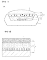
- FIG. 1 is a sectional view showing a light emitting device package 200 according to the embodiment
- FIG. 2 is an enlarged view showing a portion A of the light emitting device package 200 according to the embodiment.
- the light emitting device package 200 includes a semiconductor light emitting device 120, a first encapsulant 131 formed over the semiconductor light emitting device 120, and a second encapsulant 132 that is formed over the first encapsulant 131 and has a refractive index greater than that of the first encapsulant 131.
- the light emitting device package 200 may include a package body 110 including a cavity C, the semiconductor light emitting device 120 formed in the cavity C, the first encapsulant 131 filled in a portion of the cavity C, and the second encapsulant 132 formed over the first encapsulant 131.
- the light emitting device package 200 may be filled with at least two types of encapsulants.
- the encapsulants may include the first encapsulant (E1) 131 in the contact with the semiconductor light emitting device 120 and the second encapsulant (E2) 132 spaced apart from the semiconductor light emitting device 120.
- the refractive index of the first encapsulant (E1) 131 is less than that of the second encapsulant (E2) 132, and a phosphor P belongs to the second encapsulant (E2) 132.
- the re-introduction of a portion of a light from the phosphor P into the semiconductor light emitting device 120 can be prevented due to total reflection because the refractive index of the second encapsulant 132 is greater than that of the first encapsulant (E1) 131.
- the mold shape of the second encapsulant (E2) 132 may be a dome shape, which is convex upward, instead of a flat shape. In this case, the quantity of light may be additionally increased.
- a third encapsulant 133 having a dome shape may be formed over the second encapsulant 132 , so that the quantity of light can be increased.
- the refractive index of the third encapsulant 133 may be identical to or greater than that of the second encapsulant 132.
- FIG. 3 is a graph showing a light extraction effect as a function of a refractive index of the semiconductor light emitting device 120 according to the embodiment.
- FIG. 3 illustrates a graph representing the light extraction effect as a function of a refractive index of the first encapsulant (E1) 131 when the refractive index of the second encapsulant (E2) 132 is 1.4, and a period a of a light extracting pattern R is about 1200 nm.
- the refractive index of the semiconductor light emitting device 120 may be about 2.46, but the embodiment is not limited thereto.
- the light extracting pattern R for example, a photonic crystal structure is provided at an upper portion of the semiconductor light emitting device 120
- the refractive index of the first encapsulant 131 in the contact with the semiconductor light emitting device 120 is reduced, the light extraction effect is increased. This is because the light extraction effect is determined according to the refractive index contrast of the light extracting pattern R.
- the light extraction effect may be relatively improved.
- the refractive index of the first encapsulant 131 is reduced in a state in which the refractive index of the semiconductor light emitting device 120 is constant, the diffraction effect of the light extracting pattern R is increased. Accordingly, when the refractive index of the first encapsulant 131 is reduced, the re-introduction of alight is prevented due to the total reflection, and the light extraction efficiency can be improved.
- an LED chip and the package are designed in such a manner that the light generated from an active layer of the semiconductor light emitting device 120, and a light acquired from the phosphor P excited by the light of the active layer are prevented from being re-introduced into the LED chip, thereby realizing a high-efficiency white LED, and improving the reliability for the LED chip.
- the package body 110 including the cavity C is formed.
- the package body 110 may include a silicon substrate, but the embodiment is not limited thereto.
- the cavity C may be formed by etching a portion of the package body 110.
- the cavity C may include a bottom surface and an inclined lateral surface, but the embodiment is not limited thereto.
- the semiconductor light emitting device 120 is formed in the cavity C.
- the semiconductor light emitting device 120 may be mounted on the bottom surface of the cavity C.
- the semiconductor light emitting device 120 may be a horizontal type light emitting device or a vertical type light emitting device.
- the semiconductor light emitting device 120 may include a material selected from the group consisting of GaN, GaAs, GaAsP, and GaP.
- green and blue LEDs may include GaN (InGaN)
- yellow and red LEDs may include InGaAIP, or AIGaAs.
- Full color LEDs may be realized by changing the composition of materials.
- the semiconductor light emitting device 120 may include a first conductive semiconductor layer, a second conductive semiconductor layer, and an active layer between the first and second conductive semiconductor layers.
- the semiconductor light emitting device 120 may include the light extracting pattern R.
- the light extracting pattern R such as the photonic crystal structure may be formed at the upper portion of the semiconductor light emitting device 120.
- holes or concavo-convex patterns formed on a surface of the semiconductor light emitting device 120 have a spatial periodicity, they are called a photonic crystal.
- Several parameters of the photonic crystal such as a period, an etching depth, a hole size, and a lattice arrangement are closely related to the light extraction efficiency.
- the light extracting pattern R may include a multi-periodic photonic crystal structure (not shown). According to the multi-periodic photonic crystal structure, a smaller-periodic photonic crystal structure is inserted in a greater-periodic photonic crystal structure.
- the multi-periodic photonic structure having various periods maintains diffraction efficiency higher than that of a photonic crystal structure having one period with respect to various angles of incidence. Accordingly, the light extraction efficiency can be improved.
- the first encapsulant 131 filled in a portion of the cavity C is formed.
- the first encapsulant 131 may include silicon gel, but the embodiment is not limited thereto.
- the first encapsulant 131 may not include the phosphor P. Accordingly, the light generated from the semiconductor light emitting device 120 is not converted into light having a different wavelength in the first encapsulant 131, but passes through the first encapsulant 131.
- the first encapsulant 131 may make contact with the semiconductor light emitting device 120.
- the refractive index of the semiconductor light emitting device 120 may be greater than that of the first encapsulant 131. In this case, since the light extracting pattern R is formed at the upper portion of the semiconductor light emitting device 120, the light, which will be totally-reflected generally, is extracted to the outside of the semiconductor light emitting device 120 by the light extracting pattern R.
- the second encapsulant 132 is formed over the first encapsulant 131.
- the second encapsulant 132 is filled in the cavity C, but the embodiment is not limited thereto.
- the second encapsulant 132 may include the phosphor P. Since the light emitted by exciting the phosphor P has a wavelength longer than that of the light generated from the semiconductor light emitting device 120, the probability in which the light emitted by exciting the phosphor P is re-introduced into the semiconductor light emitting device 120 may be increased due to the light extracting pattern R. Accordingly, the phosphor P may be spaced apart from the light extracting pattern R.
- a yellow phosphor e.g., YAG, TAG, etc.
- a blue LED or three-color (red/green/blue) phosphors may be added to an UV LED.
- a yellow phosphor such as YAG or TAG, may be added to the blue LED.
- a white LED may be realized by adding two types (yellow + red) of phosphors or three (yellow+red+blue) phosphors to the blue LED.
- the white LED may be realized by using two or three types (R, G, and B) of phosphor materials. Accordingly, a phosphor absorbs all of the UV ray emitted from the UV LED such that the light having the whole wavelength bands of a visible ray can be emitted, thereby realizing a white light.
- the UV LED represents light conversion efficiency superior to a YAG phosphor constituting a conventional blue LED.
- the second encapsulant 132 may be spaced apart from the semiconductor light emitting device 120.
- the second encapsulant 132 may have a refractive index greater than that of the first encapsulant 131.
- the re-introduction of a portion of the light from the phosphor P into the semiconductor light emitting device 120 is prevented due to total reflection because the refractive index of the second encapsulant 132 is greater than that of the first encapsulant 131.
- the mold shape of the second encapsulant 132 may be a dome shape instead of a flat shape.
- the quantity of light may be additionally increased.
- the third encapsulant 133 having a dome shape may be formed over the second encapsulant 132, so that the quantity of light can be increased.
- the refractive index of the third encapsulant 133 is identical to or greater than that of the second encapsulant 132.
- the LED chip and the package are designed in such a manner that the light generated from the active layer of the semiconductor light emitting device 120, and the light acquired through the mixture of the phosphor P and the light of the active layer are prevented from being re-introduced into the LED chip, thereby realizing the high-efficiency white LED, and improving the reliability for the LED chip.
- FIG. 8 is a perspective view showing a lighting unit 1100 according to the embodiment.
- the lighting unit 1100 shown in FIG. 8 is an example of a lighting system and the embodiment is not limited thereto.
- the lighting unit 1100 includes a case body 1110, a light emitting module 1130 installed in the case body 1110, and a connection terminal 1120 installed in the case body 1110 to receive power from an external power source.
- the case body 1110 preferably includes a material having superior heat dissipation property.
- the case body 1110 includes a metallic material or a resin material.
- the light emitting module 1130 may include a substrate 1132 and at least one light emitting device package 200 installed on the substrate 1132.
- the substrate 1132 includes an insulating member printed with a circuit pattern.
- the substrate 1132 includes a PCB (printed circuit board), an MC (metal core) PCB, an F (flexible) PCB, or a ceramic PCB.
- the substrate 1132 may include a material that effectively reflects the light.
- the surface of the substrate 1132 can be coated with a color, such as a white color or a silver color, to effectively reflect the light.
- At least one light emitting device package 200 can be installed on the substrate 1132.
- Each light emitting device package 200 may include at least one LED (light emitting diode).
- the LED may include a colored LED that emits the light having the color of red, green, blue or white and a UV (ultraviolet) LED that emits UV light.
- the LEDs of the light emitting module 1130 can be variously arranged to provide various colors and brightness.
- the white LED, the red LED and the green LED can be arranged to achieve the high color rendering index (CRI).
- connection terminal 1120 is electrically connected to the light emitting module 1130 to supply power to the light emitting module 1130.
- the connection terminal 1120 has a shape of a socket screw-coupled with the external power source, but the embodiment is not limited thereto.
- the connection terminal 1120 can be prepared in the form of a pin inserted into the external power source or connected to the external power source through a wire.
- FIG. 9 is an exploded perspective view showing a backlight unit 1200 according to the embodiment.
- the backlight unit 1200 shown in FIG. 9 is an example of a lighting system and the embodiment is not limited thereto.
- the backlight unit 1200 includes a light guide plate 1210, a light emitting module 1240 for providing the light to the light guide plate 1210, a reflective member 1220 positioned under the light guide plate 1210, and a bottom cover 1230 for receiving the light guide plate 1210, light emitting module 1240, and the reflective member 1220 therein, but the embodiment is not limited thereto.
- the light guide plate 1210 diffuses the light to provide a surface light.
- the light guide 1210 includes a transparent material.
- the light guide plate 1210 can be manufactured by using acryl-based resin, such as PMMA (polymethyl methacrylate), PET (polyethylene terephthalate), PC (polycarbonate), COC or PEN (polyethylene naphthalate) resin.
- PMMA polymethyl methacrylate
- PET polyethylene terephthalate
- PC polycarbonate
- COC polycarbonate
- PEN polyethylene naphthalate
- the light emitting module 1240 supplies the light to at least one lateral side of the light guide plate 1210 and serves as the light source of the display device including the backlight unit.
- the light emitting module 1240 can be positioned adjacent to the light guide plate 1210, but the embodiment is not limited thereto.
- the light emitting module 1240 includes a substrate 1242 and a plurality of light emitting device packages 200 installed on the substrate 1242 and the substrate 1242 can be adjacent to the light guide plate 1210, but the embodiment is not limited thereto.
- the substrate 1242 may include a printed circuit board (PCB) having a circuit pattern (not shown).
- the substrate 1242 may also include a metal core PCB (MCPCB) or a flexible PCB (FPCB), but the embodiment is not limited thereto.
- PCB printed circuit board
- MCPCB metal core PCB
- FPCB flexible PCB
- the light emitting device packages 200 are arranged such that light exit surfaces of the light emitting device packages 200 are spaced apart from the light guide plate 1210 at a predetermined distance.
- the reflective member 1220 is disposed under the light guide plate 1210.
- the reflective member 1220 reflects the light, which is traveled downward through the bottom surface of the light guide plate 1210, toward the light guide plate 1210, thereby improving the brightness of the backlight unit.
- the reflective member 1220 may include PET, PC or PVC resin, but the embodiment is not limited thereto.
- the bottom cover 1230 may receive the light guide plate 1210, the light emitting module 1240, and the reflective member 1220 therein. To this end, the bottom cover 1230 has a box shape with an open top surface, but the embodiment is not limited thereto.
- the bottom cover 1230 can be manufactured through a press process or an extrusion process by using a metallic material or a resin material.
- the LED chip and a package are designed in such a manner that the light generated from the active layer of the semiconductor light emitting device, and the light acquired through the mixture of the phosphor P and the light of the active layer are prevented from being re-introduced into the LED chip, thereby realizing the high-efficiency white LED, and improving the reliability for the LED chip.
- any reference in this specification to "one embodiment, “an embodiment,” “example embodiment,” etc. means that a particular feature, structure, or characteristic described in connection with the embodiment is included in at least one embodiment of the invention.
- the appearances of such phrases in various places in the specification are not necessarily all referring to the same embodiment.
Landscapes
- Led Device Packages (AREA)
Abstract
Description
- The embodiment relates to a light emitting device package, a lighting module and a lighting system.
- A light emitting device (LED) includes a p-n junction diode having a characteristic of converting electric energy into optical energy. The p-n junction diode can be formed by combining group III elements and group V elements of the periodic table with each other. The LED can represent various colors by adjusting the compositional ratio of compound semiconductors.
- When a forward voltage is applied to the LED, electrons at an n layer are combined with holes at a p layer, so that energy corresponding to an energy gap between a conduction band and a valance band may be generated. This energy is mainly emitted as heat or light, and the LED emits the energy as the light.
- A nitride semiconductor represents superior thermal stability and wide band gap energy so that the nitride semiconductor has been spotlighted in the field of optical devices and high-power electronic devices. In particular, blue, green, and UV light emitting devices employing the nitride semiconductor have already been developed and extensively used.
- A white light emitting device (white LED) can be realized by mixing individual R, G, B light sources with each other, or converting a phosphor through a pump beam of a UV light or a blue light. The scheme of converting the phosphor has advantages in terms of the manufacturing cost, the adjustment of a color temperature, and light emission efficiency.
- Meanwhile, when the white LED is realized by utilizing the phosphor, a portion of a blue light or a UV light serving as a matrix is not absorbed into the phosphor, but extracted to the outside, and a remaining portion of the blue light or the UV light is combined with the phosphor to create a color light having a wavelength longer than that of the light of the matrix. When the extracted light and the color light are mixed with each other, white LEDs representing various color temperatures are realized according to the mixed ratios between the two lights.
- However, according to the related art, when an encapsulant mixed with a phosphor is applied or a package including an encapsulant surrounding the phosphor is employed, a portion of a created light may be re-introduced into a chip due to the refractive index contrast between the encapsulant and air that is a medium observed at the final stage.
- In addition, according to the related art, since a light converted by the phosphor creates a light having an omnidirectional characteristic in a spontaneous emission process, a portion of the light cannot but be re-introduced into the chip.
- Therefore, according to the related art, if a light is re-introduced into the chip, light emission efficiency may be reduced due to light loss caused by the light absorption in the chip. In addition, the reliability for the chip may be degraded. Accordingly, a package to prevent a light from being re-introduced into the chip has to be designed.
- The embodiment provides a light emitting device package, a lighting module and a lighting system, capable of preventing a light, which is generated from an active layer of an LED, and a light acquired through the mixture of a phosphor and the light of the active layer from being re-introduced into a chip.
- According to the embodiment, a light emitting device package includes a semiconductor light emitting device including a first conductive semiconductor layer, a second conductive semiconductor layer, and an active layer interposed between the first and second conductive semiconductor layers, a first encapsulant over the semiconductor light emitting device, and a second encapsulant having a refractive index greater than a refractive index of the first encapsulant over the first encapsulant.
- According to the embodiment, a lighting system includes a substrate, and a light emitting module including a light emitting device package mounted on the substrate.
- According to the embodiment, a lighting module includes a light emitting device package.
-
-
FIG. 1 is a sectional view showing a light emitting device package according to the embodiment; -
FIG. 2 is an enlarged view showing a portion of the light emitting device package according to the embodiment; -
FIG. 3 is a graph showing a light extraction effect as a function of a refractive index of the light emitting device package according to the embodiment; -
FIGS. 4 to 7 are sectional views showing the manufacturing process of the light emitting device package according to the embodiment; -
FIG. 8 is a perspective view showing a lighting unit according to the embodiment; and -
FIG. 9 is an exploded perspective view showing a backlight unit according to the embodiment. - Hereinafter, a light emitting device package, a lighting module and a lighting system according to the embodiment will be described with reference to accompanying drawings.
- In the description of embodiments, it will be understood that when a layer (or film) is referred to as being 'on' another layer or substrate, it can be directly on another layer or substrate, or intervening layers may also be present. Further, it will be understood that when a layer is referred to as being 'under' another layer, it can be directly under another layer, and one or more intervening layers may also be present. In addition, it will also be understood that when a layer is referred to as being `between' two layers, it can be the only layer between the two layers, or one or more intervening layers may also be present.
-
FIG. 1 is a sectional view showing a lightemitting device package 200 according to the embodiment, andFIG. 2 is an enlarged view showing a portion A of the lightemitting device package 200 according to the embodiment. - The light
emitting device package 200 according to the embodiment includes a semiconductorlight emitting device 120, afirst encapsulant 131 formed over the semiconductorlight emitting device 120, and asecond encapsulant 132 that is formed over thefirst encapsulant 131 and has a refractive index greater than that of thefirst encapsulant 131. - In addition, the light
emitting device package 200 according to the embodiment may include apackage body 110 including a cavity C, the semiconductorlight emitting device 120 formed in the cavity C, thefirst encapsulant 131 filled in a portion of the cavity C, and thesecond encapsulant 132 formed over thefirst encapsulant 131. - The light
emitting device package 200 according to the embodiment may be filled with at least two types of encapsulants. - For example, the encapsulants may include the first encapsulant (E1) 131 in the contact with the semiconductor
light emitting device 120 and the second encapsulant (E2) 132 spaced apart from the semiconductorlight emitting device 120. In this case, the refractive index of the first encapsulant (E1) 131 is less than that of the second encapsulant (E2) 132, and a phosphor P belongs to the second encapsulant (E2) 132. - According to the embodiment, the re-introduction of a portion of a light from the phosphor P into the semiconductor
light emitting device 120 can be prevented due to total reflection because the refractive index of thesecond encapsulant 132 is greater than that of the first encapsulant (E1) 131. - According to the embodiment, the mold shape of the second encapsulant (E2) 132 may be a dome shape, which is convex upward, instead of a flat shape. In this case, the quantity of light may be additionally increased.
- According to the embodiment, a
third encapsulant 133 having a dome shape may be formed over thesecond encapsulant 132 , so that the quantity of light can be increased. In this case, the refractive index of thethird encapsulant 133 may be identical to or greater than that of thesecond encapsulant 132. -
FIG. 3 is a graph showing a light extraction effect as a function of a refractive index of the semiconductorlight emitting device 120 according to the embodiment. - For example,
FIG. 3 illustrates a graph representing the light extraction effect as a function of a refractive index of the first encapsulant (E1) 131 when the refractive index of the second encapsulant (E2) 132 is 1.4, and a period a of a light extracting pattern R is about 1200 nm. In this case, the refractive index of the semiconductorlight emitting device 120 may be about 2.46, but the embodiment is not limited thereto. - As shown in
FIG. 3 , according to the embodiment, when the light extracting pattern R, for example, a photonic crystal structure is provided at an upper portion of the semiconductorlight emitting device 120, if the refractive index of thefirst encapsulant 131 in the contact with the semiconductorlight emitting device 120 is reduced, the light extraction effect is increased. This is because the light extraction effect is determined according to the refractive index contrast of the light extracting pattern R. - For example, if the refractive index of the
first encapsulant 131 is less than 1.4 that is the refractive index of thesecond encapsulant 132, the light extraction effect may be relatively improved. - If the refractive index of the
first encapsulant 131 is reduced in a state in which the refractive index of the semiconductorlight emitting device 120 is constant, the diffraction effect of the light extracting pattern R is increased. Accordingly, when the refractive index of thefirst encapsulant 131 is reduced, the re-introduction of alight is prevented due to the total reflection, and the light extraction efficiency can be improved. - According to the light
emitting device package 200 of the embodiment, an LED chip and the package are designed in such a manner that the light generated from an active layer of the semiconductorlight emitting device 120, and a light acquired from the phosphor P excited by the light of the active layer are prevented from being re-introduced into the LED chip, thereby realizing a high-efficiency white LED, and improving the reliability for the LED chip. - Hereinafter, a method of manufacturing the semiconductor
light emitting device 120 will be described with referenceFIGS. 4 to 7 . - As shown in
FIG. 4 , thepackage body 110 including the cavity C is formed. Thepackage body 110 may include a silicon substrate, but the embodiment is not limited thereto. The cavity C may be formed by etching a portion of thepackage body 110. The cavity C may include a bottom surface and an inclined lateral surface, but the embodiment is not limited thereto. - As shown in
FIG. 5 , the semiconductorlight emitting device 120 is formed in the cavity C. For example, the semiconductorlight emitting device 120 may be mounted on the bottom surface of the cavity C. In this case, the semiconductorlight emitting device 120 may be a horizontal type light emitting device or a vertical type light emitting device. - According to the embodiment, the semiconductor
light emitting device 120 may include a material selected from the group consisting of GaN, GaAs, GaAsP, and GaP. For example, green and blue LEDs may include GaN (InGaN), and yellow and red LEDs may include InGaAIP, or AIGaAs. Full color LEDs may be realized by changing the composition of materials. The semiconductorlight emitting device 120 may include a first conductive semiconductor layer, a second conductive semiconductor layer, and an active layer between the first and second conductive semiconductor layers. - In addition, the semiconductor
light emitting device 120 may include the light extracting pattern R. For example, as shown inFIG. 3 , according to the embodiment, the light extracting pattern R such as the photonic crystal structure may be formed at the upper portion of the semiconductorlight emitting device 120. - According to the embodiment, when holes or concavo-convex patterns formed on a surface of the semiconductor
light emitting device 120 have a spatial periodicity, they are called a photonic crystal. Several parameters of the photonic crystal such as a period, an etching depth, a hole size, and a lattice arrangement are closely related to the light extraction efficiency. - According to the embodiment, the light extracting pattern R may include a multi-periodic photonic crystal structure (not shown). According to the multi-periodic photonic crystal structure, a smaller-periodic photonic crystal structure is inserted in a greater-periodic photonic crystal structure.
- According to the embodiment, the multi-periodic photonic structure having various periods maintains diffraction efficiency higher than that of a photonic crystal structure having one period with respect to various angles of incidence. Accordingly, the light extraction efficiency can be improved.
- Then, as shown in
FIG. 6 , thefirst encapsulant 131 filled in a portion of the cavity C is formed. For example, thefirst encapsulant 131 may include silicon gel, but the embodiment is not limited thereto. According to the embodiment, thefirst encapsulant 131 may not include the phosphor P. Accordingly, the light generated from the semiconductorlight emitting device 120 is not converted into light having a different wavelength in thefirst encapsulant 131, but passes through thefirst encapsulant 131. - In addition, according to the embodiment, the
first encapsulant 131 may make contact with the semiconductorlight emitting device 120. - The refractive index of the semiconductor
light emitting device 120 may be greater than that of thefirst encapsulant 131. In this case, since the light extracting pattern R is formed at the upper portion of the semiconductorlight emitting device 120, the light, which will be totally-reflected generally, is extracted to the outside of the semiconductorlight emitting device 120 by the light extracting pattern R. - Thereafter, as shown in
FIG. 7 , thesecond encapsulant 132 is formed over thefirst encapsulant 131. - The
second encapsulant 132 is filled in the cavity C, but the embodiment is not limited thereto. - The
second encapsulant 132 may include the phosphor P. Since the light emitted by exciting the phosphor P has a wavelength longer than that of the light generated from the semiconductorlight emitting device 120, the probability in which the light emitted by exciting the phosphor P is re-introduced into the semiconductorlight emitting device 120 may be increased due to the light extracting pattern R. Accordingly, the phosphor P may be spaced apart from the light extracting pattern R. - According to the embodiment, in order to realize a white LED by using the phosphor P, a yellow phosphor (e.g., YAG, TAG, etc.) may be added to a blue LED, or three-color (red/green/blue) phosphors may be added to an UV LED.
- For example, according to the embodiment, a yellow phosphor, such as YAG or TAG, may be added to the blue LED.
- In addition, in the scheme of realizing the white LED by combining the blue LED with yellow phosphors, a white LED may be realized by adding two types (yellow + red) of phosphors or three (yellow+red+blue) phosphors to the blue LED.
- According to the embodiment, the white LED may be realized by using two or three types (R, G, and B) of phosphor materials. Accordingly, a phosphor absorbs all of the UV ray emitted from the UV LED such that the light having the whole wavelength bands of a visible ray can be emitted, thereby realizing a white light. The UV LED represents light conversion efficiency superior to a YAG phosphor constituting a conventional blue LED.
- According to the embodiment, the
second encapsulant 132 may be spaced apart from the semiconductorlight emitting device 120. In addition, thesecond encapsulant 132 may have a refractive index greater than that of thefirst encapsulant 131. - According to the embodiment, the re-introduction of a portion of the light from the phosphor P into the semiconductor
light emitting device 120 is prevented due to total reflection because the refractive index of thesecond encapsulant 132 is greater than that of thefirst encapsulant 131. - According to the embodiment, the mold shape of the
second encapsulant 132 may be a dome shape instead of a flat shape. In this case, the quantity of light may be additionally increased. - According to the embodiment, the
third encapsulant 133 having a dome shape may be formed over thesecond encapsulant 132, so that the quantity of light can be increased. In this case, the refractive index of thethird encapsulant 133 is identical to or greater than that of thesecond encapsulant 132. - According to the light emitting
device package 200 and the method of manufacturing the same of the embodiment, the LED chip and the package are designed in such a manner that the light generated from the active layer of the semiconductorlight emitting device 120, and the light acquired through the mixture of the phosphor P and the light of the active layer are prevented from being re-introduced into the LED chip, thereby realizing the high-efficiency white LED, and improving the reliability for the LED chip. -
FIG. 8 is a perspective view showing alighting unit 1100 according to the embodiment. Thelighting unit 1100 shown inFIG. 8 is an example of a lighting system and the embodiment is not limited thereto. - Referring to
FIG. 8 , thelighting unit 1100 includes acase body 1110, alight emitting module 1130 installed in thecase body 1110, and aconnection terminal 1120 installed in thecase body 1110 to receive power from an external power source. - Preferably, the
case body 1110 preferably includes a material having superior heat dissipation property. For example, thecase body 1110 includes a metallic material or a resin material. - The
light emitting module 1130 may include asubstrate 1132 and at least one light emittingdevice package 200 installed on thesubstrate 1132. - The
substrate 1132 includes an insulating member printed with a circuit pattern. For example, thesubstrate 1132 includes a PCB (printed circuit board), an MC (metal core) PCB, an F (flexible) PCB, or a ceramic PCB. - In addition, the
substrate 1132 may include a material that effectively reflects the light. The surface of thesubstrate 1132 can be coated with a color, such as a white color or a silver color, to effectively reflect the light. - At least one light emitting
device package 200 can be installed on thesubstrate 1132. Each light emittingdevice package 200 may include at least one LED (light emitting diode). The LED may include a colored LED that emits the light having the color of red, green, blue or white and a UV (ultraviolet) LED that emits UV light. - The LEDs of the
light emitting module 1130 can be variously arranged to provide various colors and brightness. For instance, the white LED, the red LED and the green LED can be arranged to achieve the high color rendering index (CRI). - The
connection terminal 1120 is electrically connected to thelight emitting module 1130 to supply power to thelight emitting module 1130. Referring toFIG. 8 , theconnection terminal 1120 has a shape of a socket screw-coupled with the external power source, but the embodiment is not limited thereto. For instance, theconnection terminal 1120 can be prepared in the form of a pin inserted into the external power source or connected to the external power source through a wire. -
FIG. 9 is an exploded perspective view showing abacklight unit 1200 according to the embodiment. Thebacklight unit 1200 shown inFIG. 9 is an example of a lighting system and the embodiment is not limited thereto. - The
backlight unit 1200 according to the embodiment includes alight guide plate 1210, alight emitting module 1240 for providing the light to thelight guide plate 1210, areflective member 1220 positioned under thelight guide plate 1210, and abottom cover 1230 for receiving thelight guide plate 1210, light emittingmodule 1240, and thereflective member 1220 therein, but the embodiment is not limited thereto. - The
light guide plate 1210 diffuses the light to provide a surface light. Thelight guide 1210 includes a transparent material. For instance, thelight guide plate 1210 can be manufactured by using acryl-based resin, such as PMMA (polymethyl methacrylate), PET (polyethylene terephthalate), PC (polycarbonate), COC or PEN (polyethylene naphthalate) resin. - The
light emitting module 1240 supplies the light to at least one lateral side of thelight guide plate 1210 and serves as the light source of the display device including the backlight unit. - The
light emitting module 1240 can be positioned adjacent to thelight guide plate 1210, but the embodiment is not limited thereto. In detail, thelight emitting module 1240 includes asubstrate 1242 and a plurality of light emitting device packages 200 installed on thesubstrate 1242 and thesubstrate 1242 can be adjacent to thelight guide plate 1210, but the embodiment is not limited thereto. - The
substrate 1242 may include a printed circuit board (PCB) having a circuit pattern (not shown). In addition, thesubstrate 1242 may also include a metal core PCB (MCPCB) or a flexible PCB (FPCB), but the embodiment is not limited thereto. - In addition, the light emitting device packages 200 are arranged such that light exit surfaces of the light emitting device packages 200 are spaced apart from the
light guide plate 1210 at a predetermined distance. - The
reflective member 1220 is disposed under thelight guide plate 1210. Thereflective member 1220 reflects the light, which is traveled downward through the bottom surface of thelight guide plate 1210, toward thelight guide plate 1210, thereby improving the brightness of the backlight unit. For instance, thereflective member 1220 may include PET, PC or PVC resin, but the embodiment is not limited thereto. - The
bottom cover 1230 may receive thelight guide plate 1210, thelight emitting module 1240, and thereflective member 1220 therein. To this end, thebottom cover 1230 has a box shape with an open top surface, but the embodiment is not limited thereto. - The
bottom cover 1230 can be manufactured through a press process or an extrusion process by using a metallic material or a resin material. - According to the light emitting device package and the lighting system of the embodiment, the LED chip and a package are designed in such a manner that the light generated from the active layer of the semiconductor light emitting device, and the light acquired through the mixture of the phosphor P and the light of the active layer are prevented from being re-introduced into the LED chip, thereby realizing the high-efficiency white LED, and improving the reliability for the LED chip.
- Any reference in this specification to "one embodiment, "an embodiment," "example embodiment," etc., means that a particular feature, structure, or characteristic described in connection with the embodiment is included in at least one embodiment of the invention. The appearances of such phrases in various places in the specification are not necessarily all referring to the same embodiment. Further, when a particular feature, structure, or characteristic is described in connection with any embodiment, it is submitted that it is within the purview of one skilled in the art to effect such feature, structure, or characteristic in connection with other ones of the embodiments.
- Although embodiments have been described with reference to a number of illustrative embodiments thereof, it should be understood that numerous other modifications and embodiments can be devised by those skilled in the art that will fall within the spirit and scope of the principles of this disclosure. More particularly, various variations and modifications are possible in the component parts and/or arrangements of the subject combination arrangement within the scope of the disclosure, the drawings and the appended claims. In addition to variations and modifications in the component parts and/or arrangements, alternative uses will also be apparent to those skilled in the art.
Claims (13)
- A light emitting device package comprising:a semiconductor light emitting device including a first conductive semiconductor layer, a second conductive semiconductor layer, and an active layer interposed between the first and second conductive semiconductor layers;a first encapsulant over the semiconductor light emitting device; anda second encapsulant having a refractive index greater than a refractive index of the first encapsulant over the first encapsulant.
- The light emitting device package of claim 1, wherein the first encapsulant contacts the semiconductor light emitting device.
- The light emitting device package of claim 1, wherein the second encapsulant comprises a phosphor.
- The light emitting device package of claim 1, wherein the second encapsulant is spaced apart from the semiconductor light emitting device.
- The light emitting device package of claim 1, wherein the second encapsulant comprises an upper portion in a dome shape.
- The light emitting device package of claim 1, further comprising a third encapsulant having a dome-shape upper portion over the second encapsulant.
- The light emitting device package of claim 6, wherein the third encapsulant has a refractive index greater than or equal to the refractive index of the second encapsulant.
- The light emitting device package of claim 1, wherein the semiconductor light emitting device comprises a light extracting pattern provided at an upper portion thereof.
- The light emitting device package of claim 8, wherein the light extracting pattern contacts the first encapsulant, and the second encapsulant comprises a phosphor.
- The light emitting device package of claim 8, wherein the light extracting pattern comprises a multi-periodic photonic structure.
- The light emitting device package of claim 1, wherein the semiconductor light emitting device has a refractive index greater than the refractive index of the first encapsulant.
- A lighting system comprising:a substrate; anda light emitting module including a light emitting device package according to one of claims 1 to 11 mounted on the substrate.
- A lighting module comprising:a light emitting device package according to one of claims 1 to 11 .
Applications Claiming Priority (1)
| Application Number | Priority Date | Filing Date | Title |
|---|---|---|---|
| KR1020090101227A KR101039930B1 (en) | 2009-10-23 | 2009-10-23 | Light emitting device package and manufacturing method thereof |
Publications (3)
| Publication Number | Publication Date |
|---|---|
| EP2315283A2 true EP2315283A2 (en) | 2011-04-27 |
| EP2315283A3 EP2315283A3 (en) | 2014-04-02 |
| EP2315283B1 EP2315283B1 (en) | 2017-03-29 |
Family
ID=43589763
Family Applications (1)
| Application Number | Title | Priority Date | Filing Date |
|---|---|---|---|
| EP10188574.7A Not-in-force EP2315283B1 (en) | 2009-10-23 | 2010-10-22 | Light emitting device package, lighting module and lighting unit |
Country Status (4)
| Country | Link |
|---|---|
| US (1) | US9048395B2 (en) |
| EP (1) | EP2315283B1 (en) |
| KR (1) | KR101039930B1 (en) |
| CN (1) | CN102074642B (en) |
Cited By (1)
| Publication number | Priority date | Publication date | Assignee | Title |
|---|---|---|---|---|
| WO2013054226A1 (en) * | 2011-10-12 | 2013-04-18 | Koninklijke Philips Electronics N.V. | Light-emitting arrangement |
Families Citing this family (7)
| Publication number | Priority date | Publication date | Assignee | Title |
|---|---|---|---|---|
| US8704265B2 (en) * | 2007-08-27 | 2014-04-22 | Lg Electronics Inc. | Light emitting device package and lighting apparatus using the same |
| CN103515516A (en) * | 2012-06-20 | 2014-01-15 | 鑫成科技(成都)有限公司 | Light-emitting diode packaging structure |
| KR20140028768A (en) * | 2012-08-30 | 2014-03-10 | 현대모비스 주식회사 | A lamp apparatus for automobile and manufacturing method thereof |
| CN103022310B (en) * | 2012-12-30 | 2016-03-23 | 佛山市国星半导体技术有限公司 | The light-extraction layer of LED luminescence chip and LED matrix |
| JP6582754B2 (en) * | 2015-08-31 | 2019-10-02 | 日亜化学工業株式会社 | Composite substrate, light emitting device, and method of manufacturing light emitting device |
| CN105304802A (en) * | 2015-10-12 | 2016-02-03 | 深圳万城节能股份有限公司 | Method for manufacturing light emitting device |
| TWI624966B (en) * | 2015-11-23 | 2018-05-21 | 隆達電子股份有限公司 | Light-emitting diode package |
Family Cites Families (23)
| Publication number | Priority date | Publication date | Assignee | Title |
|---|---|---|---|---|
| JP4090512B2 (en) * | 1997-04-08 | 2008-05-28 | 日本オプネクスト株式会社 | Optical module |
| US6963168B2 (en) * | 2000-08-23 | 2005-11-08 | Idemitsu Kosan Co., Ltd. | Organic EL display device having certain relationships among constituent element refractive indices |
| TW552726B (en) * | 2001-07-26 | 2003-09-11 | Matsushita Electric Works Ltd | Light emitting device in use of LED |
| JP2003197973A (en) * | 2001-12-28 | 2003-07-11 | Toshiba Lighting & Technology Corp | Light emitting diode and LED display device |
| US20050211991A1 (en) * | 2004-03-26 | 2005-09-29 | Kyocera Corporation | Light-emitting apparatus and illuminating apparatus |
| KR100576866B1 (en) * | 2004-06-16 | 2006-05-10 | 삼성전기주식회사 | Light emitting diode and manufacturing method |
| TW200614548A (en) * | 2004-07-09 | 2006-05-01 | Matsushita Electric Industrial Co Ltd | Light-emitting device |
| KR100593941B1 (en) * | 2005-04-28 | 2006-06-30 | 삼성전기주식회사 | Method of manufacturing group III nitride light emitting device |
| KR100665219B1 (en) * | 2005-07-14 | 2007-01-09 | 삼성전기주식회사 | Wavelength Converting LED Package |
| JP4778745B2 (en) * | 2005-07-27 | 2011-09-21 | パナソニック株式会社 | Semiconductor light emitting device and manufacturing method thereof |
| JP2007116131A (en) | 2005-09-21 | 2007-05-10 | Sanyo Electric Co Ltd | LED light emitting device |
| KR100867519B1 (en) * | 2006-02-02 | 2008-11-07 | 삼성전기주식회사 | Light emitting diode module |
| KR100736623B1 (en) * | 2006-05-08 | 2007-07-09 | 엘지전자 주식회사 | Vertical light emitting device and manufacturing method |
| KR100735432B1 (en) * | 2006-05-18 | 2007-07-04 | 삼성전기주식회사 | Light emitting device package and light emitting device package array |
| KR100854328B1 (en) * | 2006-07-07 | 2008-08-28 | 엘지전자 주식회사 | Light emitting device package and its manufacturing method |
| KR20080032882A (en) * | 2006-10-11 | 2008-04-16 | 삼성전기주식회사 | Light emitting diode package |
| KR100826396B1 (en) * | 2007-01-18 | 2008-05-02 | 삼성전기주식회사 | LED chip package |
| KR20090104860A (en) * | 2007-02-15 | 2009-10-06 | 파나소닉 전공 주식회사 | Installation structure of LED package and three-dimensional circuit parts |
| JP5228464B2 (en) | 2007-12-11 | 2013-07-03 | 住友大阪セメント株式会社 | LIGHT EMITTING DEVICE AND ELECTRONIC DEVICE |
| KR100849829B1 (en) * | 2008-03-18 | 2008-07-31 | 삼성전기주식회사 | Light Emitting Diode Package with Wide Angle |
| US8637883B2 (en) | 2008-03-19 | 2014-01-28 | Cree, Inc. | Low index spacer layer in LED devices |
| US7923739B2 (en) * | 2009-06-05 | 2011-04-12 | Cree, Inc. | Solid state lighting device |
| US8022434B2 (en) * | 2009-05-22 | 2011-09-20 | Unity Opto Technology Co., Ltd. | Light-emitting diode |
-
2009
- 2009-10-23 KR KR1020090101227A patent/KR101039930B1/en not_active Expired - Fee Related
-
2010
- 2010-10-21 US US12/909,098 patent/US9048395B2/en active Active
- 2010-10-22 EP EP10188574.7A patent/EP2315283B1/en not_active Not-in-force
- 2010-10-25 CN CN201010528649.2A patent/CN102074642B/en not_active Expired - Fee Related
Non-Patent Citations (1)
| Title |
|---|
| None |
Cited By (1)
| Publication number | Priority date | Publication date | Assignee | Title |
|---|---|---|---|---|
| WO2013054226A1 (en) * | 2011-10-12 | 2013-04-18 | Koninklijke Philips Electronics N.V. | Light-emitting arrangement |
Also Published As
| Publication number | Publication date |
|---|---|
| US20110095319A1 (en) | 2011-04-28 |
| CN102074642B (en) | 2015-11-25 |
| US9048395B2 (en) | 2015-06-02 |
| KR101039930B1 (en) | 2011-06-09 |
| EP2315283B1 (en) | 2017-03-29 |
| KR20110044511A (en) | 2011-04-29 |
| EP2315283A3 (en) | 2014-04-02 |
| CN102074642A (en) | 2011-05-25 |
Similar Documents
| Publication | Publication Date | Title |
|---|---|---|
| CN112136219B (en) | lighting module | |
| US9171998B2 (en) | Light emitting lamp | |
| EP2315283B1 (en) | Light emitting device package, lighting module and lighting unit | |
| KR102024291B1 (en) | Lamp unit and vehicle lamp apparatus for using the same | |
| US9897789B2 (en) | Light emitting device package and lighting device having the same | |
| US10113705B2 (en) | Light source module and lighting device having the same | |
| US9391117B2 (en) | Light emitting diode package | |
| JP2011216891A (en) | Light-emitting device package and lighting system | |
| KR20110094996A (en) | Light emitting device package, manufacturing method and lighting system | |
| KR20150002361A (en) | Semiconductor light emitting device and method for manufacturing method for light source module | |
| JP2011216886A (en) | Light emitting device and light emitting device package | |
| CN119725335A (en) | Lighting module | |
| US8053805B2 (en) | Light emitting device, light emitting device and package, and lighting system | |
| KR102300558B1 (en) | Light source module | |
| US8513697B2 (en) | Light emitting device, method of manufacturing the same, light emitting device package, and illumination system | |
| US8791482B2 (en) | Light emitting device package | |
| KR101039974B1 (en) | Light emitting device, light emitting device manufacturing method and light emitting device package | |
| EP2813758B1 (en) | Light emitting module | |
| US9222640B2 (en) | Coated diffuser cap for LED illumination device | |
| KR101666844B1 (en) | Optical device and light source module having the same | |
| EP2315275A1 (en) | Light emitting device, method of manufacturing the same, light emitting device package, and lighting system | |
| KR101724699B1 (en) | Light emitting apparatus and lighting system | |
| KR20130046286A (en) | Light emitting device package and light uint | |
| KR100712880B1 (en) | White light emitting diodes can reduce color temperature variations | |
| KR20110115320A (en) | Light emitting device package, manufacturing method and lighting system |
Legal Events
| Date | Code | Title | Description |
|---|---|---|---|
| PUAI | Public reference made under article 153(3) epc to a published international application that has entered the european phase |
Free format text: ORIGINAL CODE: 0009012 |
|
| 17P | Request for examination filed |
Effective date: 20101022 |
|
| AK | Designated contracting states |
Kind code of ref document: A2 Designated state(s): AL AT BE BG CH CY CZ DE DK EE ES FI FR GB GR HR HU IE IS IT LI LT LU LV MC MK MT NL NO PL PT RO RS SE SI SK SM TR |
|
| AX | Request for extension of the european patent |
Extension state: BA ME |
|
| PUAL | Search report despatched |
Free format text: ORIGINAL CODE: 0009013 |
|
| AK | Designated contracting states |
Kind code of ref document: A3 Designated state(s): AL AT BE BG CH CY CZ DE DK EE ES FI FR GB GR HR HU IE IS IT LI LT LU LV MC MK MT NL NO PL PT RO RS SE SI SK SM TR |
|
| AX | Request for extension of the european patent |
Extension state: BA ME |
|
| RIC1 | Information provided on ipc code assigned before grant |
Ipc: H01L 33/20 20100101ALN20140224BHEP Ipc: H01L 33/56 20100101ALI20140224BHEP Ipc: H01L 33/50 20100101ALN20140224BHEP Ipc: H01L 33/54 20100101AFI20140224BHEP |
|
| RAP1 | Party data changed (applicant data changed or rights of an application transferred) |
Owner name: LG INNOTEK CO., LTD. |
|
| RBV | Designated contracting states (corrected) |
Designated state(s): AL AT BE BG CH CY CZ DE DK EE ES FI FR GB GR HR HU IE IS IT LI LT LU LV MC MK MT NL NO PL PT RO RS SE SI SK SM TR |
|
| REG | Reference to a national code |
Ref country code: DE Ref legal event code: R079 Ref document number: 602010041071 Country of ref document: DE Free format text: PREVIOUS MAIN CLASS: H01L0033540000 Ipc: H01L0033560000 |
|
| GRAP | Despatch of communication of intention to grant a patent |
Free format text: ORIGINAL CODE: EPIDOSNIGR1 |
|
| RIC1 | Information provided on ipc code assigned before grant |
Ipc: H01L 33/54 20100101ALN20160927BHEP Ipc: H01L 33/50 20100101ALN20160927BHEP Ipc: H01L 33/56 20100101AFI20160927BHEP Ipc: H01L 33/00 20100101ALN20160927BHEP Ipc: H01L 33/20 20100101ALI20160927BHEP |
|
| INTG | Intention to grant announced |
Effective date: 20161011 |
|
| RIN1 | Information on inventor provided before grant (corrected) |
Inventor name: KIM, SUN KYUNG |
|
| STAA | Information on the status of an ep patent application or granted ep patent |
Free format text: STATUS: GRANT OF PATENT IS INTENDED |
|
| GRAS | Grant fee paid |
Free format text: ORIGINAL CODE: EPIDOSNIGR3 |
|
| GRAA | (expected) grant |
Free format text: ORIGINAL CODE: 0009210 |
|
| STAA | Information on the status of an ep patent application or granted ep patent |
Free format text: STATUS: THE PATENT HAS BEEN GRANTED |
|
| AK | Designated contracting states |
Kind code of ref document: B1 Designated state(s): AL AT BE BG CH CY CZ DE DK EE ES FI FR GB GR HR HU IE IS IT LI LT LU LV MC MK MT NL NO PL PT RO RS SE SI SK SM TR |
|
| REG | Reference to a national code |
Ref country code: GB Ref legal event code: FG4D |
|
| REG | Reference to a national code |
Ref country code: CH Ref legal event code: EP |
|
| REG | Reference to a national code |
Ref country code: AT Ref legal event code: REF Ref document number: 880491 Country of ref document: AT Kind code of ref document: T Effective date: 20170415 |
|
| REG | Reference to a national code |
Ref country code: IE Ref legal event code: FG4D |
|
| REG | Reference to a national code |
Ref country code: DE Ref legal event code: R096 Ref document number: 602010041071 Country of ref document: DE |
|
| RAP2 | Party data changed (patent owner data changed or rights of a patent transferred) |
Owner name: LG INNOTEK CO., LTD. |
|
| REG | Reference to a national code |
Ref country code: NL Ref legal event code: FP |
|
| PG25 | Lapsed in a contracting state [announced via postgrant information from national office to epo] |
Ref country code: GR Free format text: LAPSE BECAUSE OF FAILURE TO SUBMIT A TRANSLATION OF THE DESCRIPTION OR TO PAY THE FEE WITHIN THE PRESCRIBED TIME-LIMIT Effective date: 20170630 Ref country code: FI Free format text: LAPSE BECAUSE OF FAILURE TO SUBMIT A TRANSLATION OF THE DESCRIPTION OR TO PAY THE FEE WITHIN THE PRESCRIBED TIME-LIMIT Effective date: 20170329 Ref country code: NO Free format text: LAPSE BECAUSE OF FAILURE TO SUBMIT A TRANSLATION OF THE DESCRIPTION OR TO PAY THE FEE WITHIN THE PRESCRIBED TIME-LIMIT Effective date: 20170629 Ref country code: LT Free format text: LAPSE BECAUSE OF FAILURE TO SUBMIT A TRANSLATION OF THE DESCRIPTION OR TO PAY THE FEE WITHIN THE PRESCRIBED TIME-LIMIT Effective date: 20170329 Ref country code: HR Free format text: LAPSE BECAUSE OF FAILURE TO SUBMIT A TRANSLATION OF THE DESCRIPTION OR TO PAY THE FEE WITHIN THE PRESCRIBED TIME-LIMIT Effective date: 20170329 |
|
| REG | Reference to a national code |
Ref country code: AT Ref legal event code: MK05 Ref document number: 880491 Country of ref document: AT Kind code of ref document: T Effective date: 20170329 |
|
| PG25 | Lapsed in a contracting state [announced via postgrant information from national office to epo] |
Ref country code: LV Free format text: LAPSE BECAUSE OF FAILURE TO SUBMIT A TRANSLATION OF THE DESCRIPTION OR TO PAY THE FEE WITHIN THE PRESCRIBED TIME-LIMIT Effective date: 20170329 Ref country code: BG Free format text: LAPSE BECAUSE OF FAILURE TO SUBMIT A TRANSLATION OF THE DESCRIPTION OR TO PAY THE FEE WITHIN THE PRESCRIBED TIME-LIMIT Effective date: 20170629 Ref country code: SE Free format text: LAPSE BECAUSE OF FAILURE TO SUBMIT A TRANSLATION OF THE DESCRIPTION OR TO PAY THE FEE WITHIN THE PRESCRIBED TIME-LIMIT Effective date: 20170329 Ref country code: RS Free format text: LAPSE BECAUSE OF FAILURE TO SUBMIT A TRANSLATION OF THE DESCRIPTION OR TO PAY THE FEE WITHIN THE PRESCRIBED TIME-LIMIT Effective date: 20170329 |
|
| PG25 | Lapsed in a contracting state [announced via postgrant information from national office to epo] |
Ref country code: CZ Free format text: LAPSE BECAUSE OF FAILURE TO SUBMIT A TRANSLATION OF THE DESCRIPTION OR TO PAY THE FEE WITHIN THE PRESCRIBED TIME-LIMIT Effective date: 20170329 Ref country code: AT Free format text: LAPSE BECAUSE OF FAILURE TO SUBMIT A TRANSLATION OF THE DESCRIPTION OR TO PAY THE FEE WITHIN THE PRESCRIBED TIME-LIMIT Effective date: 20170329 Ref country code: ES Free format text: LAPSE BECAUSE OF FAILURE TO SUBMIT A TRANSLATION OF THE DESCRIPTION OR TO PAY THE FEE WITHIN THE PRESCRIBED TIME-LIMIT Effective date: 20170329 Ref country code: RO Free format text: LAPSE BECAUSE OF FAILURE TO SUBMIT A TRANSLATION OF THE DESCRIPTION OR TO PAY THE FEE WITHIN THE PRESCRIBED TIME-LIMIT Effective date: 20170329 Ref country code: EE Free format text: LAPSE BECAUSE OF FAILURE TO SUBMIT A TRANSLATION OF THE DESCRIPTION OR TO PAY THE FEE WITHIN THE PRESCRIBED TIME-LIMIT Effective date: 20170329 Ref country code: SK Free format text: LAPSE BECAUSE OF FAILURE TO SUBMIT A TRANSLATION OF THE DESCRIPTION OR TO PAY THE FEE WITHIN THE PRESCRIBED TIME-LIMIT Effective date: 20170329 Ref country code: IT Free format text: LAPSE BECAUSE OF FAILURE TO SUBMIT A TRANSLATION OF THE DESCRIPTION OR TO PAY THE FEE WITHIN THE PRESCRIBED TIME-LIMIT Effective date: 20170329 |
|
| PG25 | Lapsed in a contracting state [announced via postgrant information from national office to epo] |
Ref country code: IS Free format text: LAPSE BECAUSE OF FAILURE TO SUBMIT A TRANSLATION OF THE DESCRIPTION OR TO PAY THE FEE WITHIN THE PRESCRIBED TIME-LIMIT Effective date: 20170729 Ref country code: PT Free format text: LAPSE BECAUSE OF FAILURE TO SUBMIT A TRANSLATION OF THE DESCRIPTION OR TO PAY THE FEE WITHIN THE PRESCRIBED TIME-LIMIT Effective date: 20170731 Ref country code: SM Free format text: LAPSE BECAUSE OF FAILURE TO SUBMIT A TRANSLATION OF THE DESCRIPTION OR TO PAY THE FEE WITHIN THE PRESCRIBED TIME-LIMIT Effective date: 20170329 Ref country code: PL Free format text: LAPSE BECAUSE OF FAILURE TO SUBMIT A TRANSLATION OF THE DESCRIPTION OR TO PAY THE FEE WITHIN THE PRESCRIBED TIME-LIMIT Effective date: 20170329 |
|
| REG | Reference to a national code |
Ref country code: DE Ref legal event code: R097 Ref document number: 602010041071 Country of ref document: DE |
|
| PG25 | Lapsed in a contracting state [announced via postgrant information from national office to epo] |
Ref country code: DK Free format text: LAPSE BECAUSE OF FAILURE TO SUBMIT A TRANSLATION OF THE DESCRIPTION OR TO PAY THE FEE WITHIN THE PRESCRIBED TIME-LIMIT Effective date: 20170329 |
|
| PLBE | No opposition filed within time limit |
Free format text: ORIGINAL CODE: 0009261 |
|
| STAA | Information on the status of an ep patent application or granted ep patent |
Free format text: STATUS: NO OPPOSITION FILED WITHIN TIME LIMIT |
|
| 26N | No opposition filed |
Effective date: 20180103 |
|
| PG25 | Lapsed in a contracting state [announced via postgrant information from national office to epo] |
Ref country code: MC Free format text: LAPSE BECAUSE OF FAILURE TO SUBMIT A TRANSLATION OF THE DESCRIPTION OR TO PAY THE FEE WITHIN THE PRESCRIBED TIME-LIMIT Effective date: 20170329 Ref country code: SI Free format text: LAPSE BECAUSE OF FAILURE TO SUBMIT A TRANSLATION OF THE DESCRIPTION OR TO PAY THE FEE WITHIN THE PRESCRIBED TIME-LIMIT Effective date: 20170329 |
|
| REG | Reference to a national code |
Ref country code: CH Ref legal event code: PL |
|
| REG | Reference to a national code |
Ref country code: NL Ref legal event code: MM Effective date: 20171101 |
|
| GBPC | Gb: european patent ceased through non-payment of renewal fee |
Effective date: 20171022 |
|
| REG | Reference to a national code |
Ref country code: IE Ref legal event code: MM4A |
|
| REG | Reference to a national code |
Ref country code: FR Ref legal event code: ST Effective date: 20180629 |
|
| PG25 | Lapsed in a contracting state [announced via postgrant information from national office to epo] |
Ref country code: GB Free format text: LAPSE BECAUSE OF NON-PAYMENT OF DUE FEES Effective date: 20171022 Ref country code: NL Free format text: LAPSE BECAUSE OF NON-PAYMENT OF DUE FEES Effective date: 20171101 Ref country code: LI Free format text: LAPSE BECAUSE OF NON-PAYMENT OF DUE FEES Effective date: 20171031 Ref country code: CH Free format text: LAPSE BECAUSE OF NON-PAYMENT OF DUE FEES Effective date: 20171031 Ref country code: LU Free format text: LAPSE BECAUSE OF NON-PAYMENT OF DUE FEES Effective date: 20171022 |
|
| REG | Reference to a national code |
Ref country code: BE Ref legal event code: MM Effective date: 20171031 |
|
| PG25 | Lapsed in a contracting state [announced via postgrant information from national office to epo] |
Ref country code: FR Free format text: LAPSE BECAUSE OF NON-PAYMENT OF DUE FEES Effective date: 20171031 Ref country code: BE Free format text: LAPSE BECAUSE OF NON-PAYMENT OF DUE FEES Effective date: 20171031 |
|
| PG25 | Lapsed in a contracting state [announced via postgrant information from national office to epo] |
Ref country code: MT Free format text: LAPSE BECAUSE OF NON-PAYMENT OF DUE FEES Effective date: 20171022 |
|
| PG25 | Lapsed in a contracting state [announced via postgrant information from national office to epo] |
Ref country code: IE Free format text: LAPSE BECAUSE OF NON-PAYMENT OF DUE FEES Effective date: 20171022 |
|
| PG25 | Lapsed in a contracting state [announced via postgrant information from national office to epo] |
Ref country code: HU Free format text: LAPSE BECAUSE OF FAILURE TO SUBMIT A TRANSLATION OF THE DESCRIPTION OR TO PAY THE FEE WITHIN THE PRESCRIBED TIME-LIMIT; INVALID AB INITIO Effective date: 20101022 |
|
| PG25 | Lapsed in a contracting state [announced via postgrant information from national office to epo] |
Ref country code: CY Free format text: LAPSE BECAUSE OF NON-PAYMENT OF DUE FEES Effective date: 20170329 |
|
| PG25 | Lapsed in a contracting state [announced via postgrant information from national office to epo] |
Ref country code: MK Free format text: LAPSE BECAUSE OF FAILURE TO SUBMIT A TRANSLATION OF THE DESCRIPTION OR TO PAY THE FEE WITHIN THE PRESCRIBED TIME-LIMIT Effective date: 20170329 |
|
| PG25 | Lapsed in a contracting state [announced via postgrant information from national office to epo] |
Ref country code: TR Free format text: LAPSE BECAUSE OF FAILURE TO SUBMIT A TRANSLATION OF THE DESCRIPTION OR TO PAY THE FEE WITHIN THE PRESCRIBED TIME-LIMIT Effective date: 20170329 |
|
| PG25 | Lapsed in a contracting state [announced via postgrant information from national office to epo] |
Ref country code: AL Free format text: LAPSE BECAUSE OF FAILURE TO SUBMIT A TRANSLATION OF THE DESCRIPTION OR TO PAY THE FEE WITHIN THE PRESCRIBED TIME-LIMIT Effective date: 20170329 |
|
| REG | Reference to a national code |
Ref country code: DE Ref legal event code: R081 Ref document number: 602010041071 Country of ref document: DE Owner name: SUZHOU LEKIN SEMICONDUCTOR CO. LTD., TAICANG, CN Free format text: FORMER OWNER: LG INNOTEK CO., LTD., SEOUL/SOUL, KR |
|
| PGFP | Annual fee paid to national office [announced via postgrant information from national office to epo] |
Ref country code: DE Payment date: 20230906 Year of fee payment: 14 |
|
| REG | Reference to a national code |
Ref country code: DE Ref legal event code: R079 Ref document number: 602010041071 Country of ref document: DE Free format text: PREVIOUS MAIN CLASS: H01L0033560000 Ipc: H10H0020854000 |
|
| REG | Reference to a national code |
Ref country code: DE Ref legal event code: R119 Ref document number: 602010041071 Country of ref document: DE |
|
| PG25 | Lapsed in a contracting state [announced via postgrant information from national office to epo] |
Ref country code: DE Free format text: LAPSE BECAUSE OF NON-PAYMENT OF DUE FEES Effective date: 20250501 |