EP2313900B1 - Substrate with embedded patterned capacitance - Google Patents
Substrate with embedded patterned capacitance Download PDFInfo
- Publication number
- EP2313900B1 EP2313900B1 EP09803461.4A EP09803461A EP2313900B1 EP 2313900 B1 EP2313900 B1 EP 2313900B1 EP 09803461 A EP09803461 A EP 09803461A EP 2313900 B1 EP2313900 B1 EP 2313900B1
- Authority
- EP
- European Patent Office
- Prior art keywords
- forming
- laminate
- conductive
- substrate
- conductive foil
- Prior art date
- Legal status (The legal status is an assumption and is not a legal conclusion. Google has not performed a legal analysis and makes no representation as to the accuracy of the status listed.)
- Active
Links
Images


Classifications
-
- H—ELECTRICITY
- H05—ELECTRIC TECHNIQUES NOT OTHERWISE PROVIDED FOR
- H05K—PRINTED CIRCUITS; CASINGS OR CONSTRUCTIONAL DETAILS OF ELECTRIC APPARATUS; MANUFACTURE OF ASSEMBLAGES OF ELECTRICAL COMPONENTS
- H05K1/00—Printed circuits
- H05K1/16—Printed circuits incorporating printed electric components, e.g. printed resistors, capacitors or inductors
- H05K1/162—Printed circuits incorporating printed electric components, e.g. printed resistors, capacitors or inductors incorporating printed capacitors
-
- H—ELECTRICITY
- H01—ELECTRIC ELEMENTS
- H01G—CAPACITORS; CAPACITORS, RECTIFIERS, DETECTORS, SWITCHING DEVICES, LIGHT-SENSITIVE OR TEMPERATURE-SENSITIVE DEVICES OF THE ELECTROLYTIC TYPE
- H01G9/00—Electrolytic capacitors, rectifiers, detectors, switching devices, light-sensitive or temperature-sensitive devices; Processes of their manufacture
- H01G9/004—Details
- H01G9/008—Terminals
- H01G9/012—Terminals specially adapted for solid capacitors
-
- H—ELECTRICITY
- H01—ELECTRIC ELEMENTS
- H01G—CAPACITORS; CAPACITORS, RECTIFIERS, DETECTORS, SWITCHING DEVICES, LIGHT-SENSITIVE OR TEMPERATURE-SENSITIVE DEVICES OF THE ELECTROLYTIC TYPE
- H01G9/00—Electrolytic capacitors, rectifiers, detectors, switching devices, light-sensitive or temperature-sensitive devices; Processes of their manufacture
- H01G9/004—Details
- H01G9/04—Electrodes or formation of dielectric layers thereon
- H01G9/042—Electrodes or formation of dielectric layers thereon characterised by the material
-
- H—ELECTRICITY
- H01—ELECTRIC ELEMENTS
- H01G—CAPACITORS; CAPACITORS, RECTIFIERS, DETECTORS, SWITCHING DEVICES, LIGHT-SENSITIVE OR TEMPERATURE-SENSITIVE DEVICES OF THE ELECTROLYTIC TYPE
- H01G9/00—Electrolytic capacitors, rectifiers, detectors, switching devices, light-sensitive or temperature-sensitive devices; Processes of their manufacture
- H01G9/004—Details
- H01G9/04—Electrodes or formation of dielectric layers thereon
- H01G9/042—Electrodes or formation of dielectric layers thereon characterised by the material
- H01G9/045—Electrodes or formation of dielectric layers thereon characterised by the material based on aluminium
-
- H—ELECTRICITY
- H01—ELECTRIC ELEMENTS
- H01G—CAPACITORS; CAPACITORS, RECTIFIERS, DETECTORS, SWITCHING DEVICES, LIGHT-SENSITIVE OR TEMPERATURE-SENSITIVE DEVICES OF THE ELECTROLYTIC TYPE
- H01G9/00—Electrolytic capacitors, rectifiers, detectors, switching devices, light-sensitive or temperature-sensitive devices; Processes of their manufacture
- H01G9/15—Solid electrolytic capacitors
-
- H—ELECTRICITY
- H05—ELECTRIC TECHNIQUES NOT OTHERWISE PROVIDED FOR
- H05K—PRINTED CIRCUITS; CASINGS OR CONSTRUCTIONAL DETAILS OF ELECTRIC APPARATUS; MANUFACTURE OF ASSEMBLAGES OF ELECTRICAL COMPONENTS
- H05K2201/00—Indexing scheme relating to printed circuits covered by H05K1/00
- H05K2201/03—Conductive materials
- H05K2201/032—Materials
- H05K2201/0329—Intrinsically conductive polymer [ICP]; Semiconductive polymer
-
- H—ELECTRICITY
- H05—ELECTRIC TECHNIQUES NOT OTHERWISE PROVIDED FOR
- H05K—PRINTED CIRCUITS; CASINGS OR CONSTRUCTIONAL DETAILS OF ELECTRIC APPARATUS; MANUFACTURE OF ASSEMBLAGES OF ELECTRICAL COMPONENTS
- H05K2201/00—Indexing scheme relating to printed circuits covered by H05K1/00
- H05K2201/03—Conductive materials
- H05K2201/0332—Structure of the conductor
- H05K2201/0335—Layered conductors or foils
- H05K2201/0355—Metal foils
-
- H—ELECTRICITY
- H05—ELECTRIC TECHNIQUES NOT OTHERWISE PROVIDED FOR
- H05K—PRINTED CIRCUITS; CASINGS OR CONSTRUCTIONAL DETAILS OF ELECTRIC APPARATUS; MANUFACTURE OF ASSEMBLAGES OF ELECTRICAL COMPONENTS
- H05K2201/00—Indexing scheme relating to printed circuits covered by H05K1/00
- H05K2201/09—Shape and layout
- H05K2201/09209—Shape and layout details of conductors
- H05K2201/095—Conductive through-holes or vias
- H05K2201/09509—Blind vias, i.e. vias having one side closed
-
- H—ELECTRICITY
- H05—ELECTRIC TECHNIQUES NOT OTHERWISE PROVIDED FOR
- H05K—PRINTED CIRCUITS; CASINGS OR CONSTRUCTIONAL DETAILS OF ELECTRIC APPARATUS; MANUFACTURE OF ASSEMBLAGES OF ELECTRICAL COMPONENTS
- H05K2201/00—Indexing scheme relating to printed circuits covered by H05K1/00
- H05K2201/09—Shape and layout
- H05K2201/09209—Shape and layout details of conductors
- H05K2201/09654—Shape and layout details of conductors covering at least two types of conductors provided for in H05K2201/09218 - H05K2201/095
- H05K2201/09763—Printed component having superposed conductors, but integrated in one circuit layer
-
- H—ELECTRICITY
- H05—ELECTRIC TECHNIQUES NOT OTHERWISE PROVIDED FOR
- H05K—PRINTED CIRCUITS; CASINGS OR CONSTRUCTIONAL DETAILS OF ELECTRIC APPARATUS; MANUFACTURE OF ASSEMBLAGES OF ELECTRICAL COMPONENTS
- H05K2201/00—Indexing scheme relating to printed circuits covered by H05K1/00
- H05K2201/09—Shape and layout
- H05K2201/09818—Shape or layout details not covered by a single group of H05K2201/09009 - H05K2201/09809
- H05K2201/09909—Special local insulating pattern, e.g. as dam around component
-
- H—ELECTRICITY
- H05—ELECTRIC TECHNIQUES NOT OTHERWISE PROVIDED FOR
- H05K—PRINTED CIRCUITS; CASINGS OR CONSTRUCTIONAL DETAILS OF ELECTRIC APPARATUS; MANUFACTURE OF ASSEMBLAGES OF ELECTRICAL COMPONENTS
- H05K2203/00—Indexing scheme relating to apparatus or processes for manufacturing printed circuits covered by H05K3/00
- H05K2203/03—Metal processing
- H05K2203/0315—Oxidising metal
-
- H—ELECTRICITY
- H05—ELECTRIC TECHNIQUES NOT OTHERWISE PROVIDED FOR
- H05K—PRINTED CIRCUITS; CASINGS OR CONSTRUCTIONAL DETAILS OF ELECTRIC APPARATUS; MANUFACTURE OF ASSEMBLAGES OF ELECTRICAL COMPONENTS
- H05K3/00—Apparatus or processes for manufacturing printed circuits
- H05K3/40—Forming printed elements for providing electric connections to or between printed circuits
- H05K3/42—Plated through-holes or plated via connections
- H05K3/429—Plated through-holes specially for multilayer circuits, e.g. having connections to inner circuit layers
-
- Y—GENERAL TAGGING OF NEW TECHNOLOGICAL DEVELOPMENTS; GENERAL TAGGING OF CROSS-SECTIONAL TECHNOLOGIES SPANNING OVER SEVERAL SECTIONS OF THE IPC; TECHNICAL SUBJECTS COVERED BY FORMER USPC CROSS-REFERENCE ART COLLECTIONS [XRACs] AND DIGESTS
- Y10—TECHNICAL SUBJECTS COVERED BY FORMER USPC
- Y10T—TECHNICAL SUBJECTS COVERED BY FORMER US CLASSIFICATION
- Y10T29/00—Metal working
- Y10T29/43—Electric condenser making
- Y10T29/435—Solid dielectric type
Definitions
- the present invention is related to an improved method for forming a capacitor. More specifically, the present invention is related to a method for forming a circuit board having capacitors formed therein.
- Capacitors are utilized in virtually every electronic device. Their function in an electronic circuit is well known and further discussion is not warranted herein.
- a second approach to miniaturization is to combine functionality in selected components.
- the real estate represented by the circuit board substrate functions, by and large, as structural support and for connectivity only and it does not otherwise contribute to the electrical function of the electrical circuit.
- Incorporating functionality into the area occupied by the substrate would serve two functions.
- a component which would otherwise be surface mounted, or otherwise incorporated, could be eliminated and the substrate space which is otherwise functionless can be reclaimed. While this is straightforward in theory, actually incorporating the functionality within the substrate has been difficult to implement in many applications. Gains have been made toward incorporating individual capacitors into a circuit substrate, as presented in U.S. Patent No.
- US 2007/094871 A1 discloses a method for manufacturing a printed circuit board with a film capacitor embedded therein and a printed circuit board obtained thereby.
- a lower electrode is formed on an insulating substrate.
- An amorphous dielectric film is formed on the lower electrode by low temperature film formation.
- a metal seed layer is formed on the dielectric film by electroless plating.
- An upper electrode is formed on the metal seed layer by electrolytic plating.
- EP 1 737 283 A1 discloses a method of embedding thick-film fired-on-foil capacitors which includes entirely covering the dielectric with an encapsulating electrode to avoid cracking in the dielectric due to shrinkage and temperature coefficient of expansion differences between the electrode and dielectric.
- US 2007/178412 A1 discloses a method for manufacturing a printed circuit board with a thin film capacitor embedded therein and a conductive metal is sputtered via a first mask to form a lower electrode.
- a dielectric material is sputtered via a second mask to form a dielectric layer.
- the conductive metal is sputtered via a third mask to form an upper electrode.
- An insulating layer is stacked on a stack body with the upper electrode formed therein and via holes are perforated from a top surface of the insulating layer to a top surface of the lower electrode and from the top surface of the insulating layer to a top surface of the upper electrode formed on the substrate.
- the stack body with the via holes formed therein is electrolytically and electrolessly plated
- US 2003/0090858 A1 discloses a method for manufacturing a component with capacitive characteristics wherein the electrolytic capacitor can be highly integrated into circuit.
- the present invention is directed to a simple and cost-effective method for incorporating large capacitance into a substrate during manufacture.
- US 2007/094871 A1 discloses a method for manufacturing a printed circuit board with a film capacitor embedded therein and a printed circuit board obtained thereby.
- a lower electrode is formed on an insulating substrate.
- An amorphous dielectric film is formed on the lower electrode by low temperature film formation.
- a metal seed layer is formed on the dielectric film by electroless plating.
- An upper electrode is formed on the metal seed layer by electrolytic plating.
- EP 1 737 283 A1 discloses a method of embedding thick-film fired-on-foil capacitors including entirely covering the dielectric with an encapsulating electrode to avoid cracking in the dielectric due to shrinkage and temperature coefficient of expansion differences between the electrode and dielectric.
- US 2007/178412 A1 discloses a method for manufacturing a printed circuit board with a thin film capacitor embedded therein, in which a conductive metal is sputtered via a first mask to form a lower electrode. A dielectric material is sputtered via a second mask to form a dielectric layer. The conductive metal is sputtered via a third mask to form an upper electrode. An insulating layer is stacked on a stack body with the upper electrode formed therein and via holes are perforated from a top surface of the insulating layer to a top surface of the lower electrode and from the top surface of the insulating layer to a top surface of the upper electrode formed on the substrate. Also, the stack body with the via holes formed therein is electrolytically and electrolessly plated.
- US 2006/020 79 70 A1 discloses a method for fabricating a patterned embedded capacitance layer.
- the method includes fabricating a ceramic oxide layer overlying a conductive metal layer overlying a printed circuit substrate, perforating the ceramic oxide layer within a region, and removing the ceramic oxide layer and the conductive metal layer in the region by chemical etching of the conductive metal layer.
- the ceramic oxide layer may be less than 1 micron thick.
- GB 148 19 04 A discloses a method of manufacturing a capacitor comprising applying over an insulating layer on a metal base a pattern of tracks of insulating material so as to divide the surface into a regular array of areas, applying a conductive layer over the areas and tracks and cutting the assembly along the tracks to form individual capacitors.
- the capacitor may be electrolytic, the base forming the anode being Nb, Ta, Ti or Hf and layer being the oxide of the base metal, and a semiconducting layer of lead oxide or manganese dioxide being applied thereto.
- a particular feature of the present invention is a method of manufacturing a capacitor integrated into a substrate.
- a particular advantage of the present invention is the ability to reclaim real estate within an electrical circuit which otherwise provides no contribution to the electronics of the circuit.
- Another advantage of the present invention is the ability to eliminate a surface mounted component by incorporating the function thereof into the substrate or circuit board.
- Yet another embodiment is provided in a capacitor formed by the above method and comprising the above layered substrate.
- Described is a process for forming a capacitor which is integral to a printed circuit board or substrate. More specifically, the invention describes a process for manufacturing a printed circuit board, or substrate, with capacitance integral thereto.
- the substrate, with an integral capacitor will be further processed by the incorporation of additional layers to form a completed substrate with a capacitor embedded therein.
- a conductive foil, 12, is attached, adhered, or laminated to an unfinished substrate, 10.
- the conductive foil comprises a dielectric layer, 13, formed on at least that surface which is away from the substrate.
- the dielectric layer can be formed after the foil is on the substrate but prior formation is preferred.
- the conductive foil is preferably a valve metal selected from aluminum, tantalum, niobium, titanium or a combination thereof or a conductive oxide such as NbO.
- the conductive foil will ultimately form the anode.
- the dielectric is preferably formed by anodic oxidation of the foil.
- both sides of the foil can contain an oxide layer.
- Metal foil with a single oxide layer is not commercially available under favorable terms, thereby necessitating the use of a foil with both sides oxidized. It is preferred that the surface of the conductive foil is roughened to increase the surface area prior to anodizing to form the oxide dielectric.
- the dielectric can be formed by other methods including vapor deposition, sol-gel applications, and solvent based applications, and may be an oxide of the conductive foil or a different material, such as a ceramic dielectric.
- a solid electrolyte layer, 14, is formed on the exposed dielectric layer, 13, in regions where the capacitive functionality is desired.
- the solid electrolyte layer may consist of one or more layers of one or more conductive polymers.
- Preferred conductive polymers include polypyrrole, polyaniline, and polythiophene.
- polypyrrole, polyaniline, and polythiophene refer equally to derivatives thereof.
- the conductive polymer may be applied from a solution or suspension or the conductive polymer may be formed in-situ by coating a monomer and oxidizer sequentially.
- In-situ polymer formation from monomer is less preferred due to the complexities of incorporating the process into conventional in-line automated processes since the number of process steps is necessarily increased with in-situ formation. Furthermore, in-situ polymer formation from monomer typically provides a thicker, less dense, polymer layer which is less desirable in most applications.
- the polymer layer is applied by any technique available in the art, without limit, with exemplary methods including ink jet printing, screen-printing, gravure coating, or masked spraying.
- the solid electrolyte layer may comprise a manganese dioxide layer either in addition to a polymer layer or instead of the polymer layer.
- the manganese dioxide layer is preferably formed by applying a solution of a manganese compound, such as manganese nitrate or a permanganate, followed by converting the manganese compound to manganese dioxide by heat. It is preferable that the manganese dioxide layer be deposited prior to deposition of the polymer; however, they can be added as a mixture.
- a manganese compound such as manganese nitrate or a permanganate
- a carbon layer, 16, is preferably applied over the solid electrolyte layer, 14, as illustrated schematically in top view in Fig. 4 and in schematic cross-sectional view in Fig. 5 taken along line 5-5 of Fig. 4 .
- the carbon layer improves adhesion between the solid electrolyte layer, 14, and subsequent conductive layer, 18, and is therefore preferred.
- the carbon layer is formed on the patterned surface of the solid electrolyte layer by applying a paste, or thick ink, containing carbon particles preferably in the form of graphite or carbon black.
- the carbon layer can be applied by ink jet printing, screen-printing, gravure printing or by spraying without limit thereto.
- the conductive layer, 18, is a layer which allows formation of a highly conductive connection between the cathode and subsequent circuitry.
- the conductive layer may be silver, copper, gold, or another highly conductive metal or a combination thereof. Particularly preferred is a silver, copper or silver/copper ink or paste.
- the layer may be deposited by ink jet printing, screen printing, gravure printing, spraying, sputtering, atomic layer deposition or other means for applying a thin layer deposition.
- the cathode refers to either the solid electrolyte layer or the combination of the solid electrolyte layer, carbon layer and conductive layer.
- each capacitive couple is preferably isolated from the others by a demarcation, 20, in the foil, which electrically isolates that portion of the foil acting as the anode and forming a capacitor with the cathode layers from the remaining foil.
- the demarcation can be formed by etching or dicing at least through the oxide layer and the valve metal foil layer. It would be apparent that that the kerf width of the demarcation must be sufficiently wide to avoid current crossing the demarcation.
- the demarcation is illustrated as a narrow strip, it is understood that it may include any or all of the foil which is not functioning as the anode of a capacitor with the understanding that a sufficient area of foil is removed to avoid current flow from the anode portion to surrounding functioning foil.
- a width of about 0.025 mm is sufficient. However, 0.05 mm is more preferable.
- foil may remain in the finished substrate, wherein the remaining foil provides either no electrical function or functions as a component in an element other than a capacitor.
- windows and holes may be created in the foil base before application of the foil to the semi-finished substrate, or these areas may be removed subsequent to the application. The holes or windows will allow vias and plated through holes to pass through this layer without connection to any of the capacitive elements and will facilitate registration of the foil during the lamination process.
- the conductive foil may remain intact between capacitors, thereby ultimately forming multiple capacitors with a common anode. Ground and power connections could then be established between at least two of the multiple cathodes without connecting to the conductive foil anode, comprising a capacitor device connected in a non-polar configuration.
- This could allow greater flexibility in the design of a circuit substrate in that an embedded capacitance layer with a given isolation dam and cathode application pattern could be utilized for more than one circuit substrate design.
- the isolation dam is a non- conductive region formed by treating the conductive material to render it non- conductive.
- a functional capacitor or multiple capacitors, is provided on a substrate and the substrate may be suitable for use in some applications.
- the demarcations may completely sever one or more junctional capacitors mounted on a substrate from the larger substrate for use.
- further processing ensues to prepare a printed circuit board with capacitance incorporated therein.
- additional circuit board material 21, over the capacitor and semi-finished substrate, thereby forming the embedded capacitance or an embedded capacitor within the substrate material.
- the additional circuit board layers are applied by any technique known in the art and standard materials are suitable for use therein. After lamination, and in the course of forming additional layers of the circuit board material, the anode and cathode terminals of the capacitor must be accessed for connection to eventual circuit traces on the circuit board.
- the connectivity among layers is preferably made with a blind via or a through hole, both of which will be described, while traces of conductive material (i.e. copper) afford connection to multiple areas at each layer.
- conductive material i.e. copper
- a cathodic blind via, 22, is formed directly above the cathode region of the capacitor. This allows a conductor to be brought into electrical contact with both the cathode and a cathodic circuit trace, 24, which may be at least temporarily on the surface of the circuit substrate.
- An anodic blind via, 26, is formed which is in electrical contact with the conductive foil forming the anode interior to the demarcation relative to the capacitive couple. The anodic blind via allows a conductor therein to form an electrical contact between the anode and an anode circuit trace, 28.
- An anodic through via, 30, passing through the entire substrate, is in electrical contact with the anode interior to the demarcation relative to the capacitive couple and is then in electrical contact with at least one anodic trace, 32, on a surface of the circuit substrate. It would be apparent that additional laminations may occur such that the traces described are ultimately interior to a layered circuit board.
- FIG. 7-11 An embodiment of the present invention will be described with reference to Figs. 7-11 .
- the substrate, 10, foil, 12, and dielectric, 13, are as described above.
- An isolation dam, 40 is formed on the surface of the dielectric.
- the interior area of the dam is the shape and size of the intended cathode and the isolation dam circumvents the cathode.
- the isolation dam prior to formation of a cathode is illustrated in top schematic view in Fig. 7 and cross-sectional schematic view in Fig. 8 taken along line 8-8 of Fig. 7 .
- a solid electrolyte and optional but preferred carbon and conductive layers are formed within the area of the isolation dam to form the cathode of a capacitor.
- the resulting capacitor is illustrated in top schematic view in Fig. 9 and in schematic cross-sectional view in Fig. 10 taken along line 10-10 of Fig. 9 .
- the isolation dam, 40 forms a pool within which the cathode, 42, is coated.
- an optional but preferred metal layer, 44 is formed and the capacitors are singulated.
- the substrate is diced along a line, 46, to isolate one or more discrete capacitor(s) on a substrate.
- the line, 46 represents a demarcation line wherein the conductive foil is interrupted between capacitors to electrically isolate discrete capacitors on a common substrate or to form discrete capacitors with a common anode.
- the demarcation can represent a narrow band which is sufficiently wide for electrical isolation, or a portion, up to the entire foil not otherwise functioning as the anode of a capacitor, can be removed.
- FIG. 11 A particularly preferred embodiment is illustrated schematically after further processing in Fig. 11 . Shown therein is additional circuit board material, 41, laminated over the capacitor. As would be apparent, electrical connectivity must be made between the capacitor and traces for the function of the capacitor to be realized in an electrical circuit. Illustrated in Fig. 11 are blind vias, 48, primarily for the cathodic couple, wherein the cathode is in electrical contact with a cathode trace, 50. Through vias, 52, are preferably formed through the isolation dam, 40, such that the isolation dam forms a sleeve with the through via therein.
- a conductor dispensed in the through via forms an electrical connection between the conductive foil, which functions as the anode, and an anode trace, 54, on at least one side of the laminated device. It would be apparent from the figure that a blind via through the isolation dam could also be utilized, wherein the blind via does not pass entirely through the structure but only through to the extent necessary to be in electrical contact with the conductive foil anode.
- a substrate, 126 has a foil laminated thereon.
- the foil comprises a first conductive layer, 128, such as a metal foil, and dielectric, 130.
- a cathode comprising a solid electrolyte, 134, and a second conductive layer, 136, is formed on the dielectric, such that the cathode and foil form a capacitive couple with the dielectric therebetween.
- the capacitive couple is isolated electrically by demarcations, 132.
- An isolation dam, 122 provides a via location for connection to the anode which is isolated from the remaining foil by the demarcation.
- a second isolation dam, 138 is provided wherein a through hole, 238, is ultimately formed for additional functionality.
- FIG. 14 An additional example is illustrated in schematic cross-sectional side view in Fig. 14 .
- the substrate, 126, first conductive layer, 128, dielectric, 130, demarcation, 132, solid electrolyte layer, 134, isolation dam, 122, and second isolation dam, 138 are as described with reference to Figs. 12 and 13 .
- additional lamination, 140 has been added to encase the capacitor elements, thereby forming a laminated substrate with embedded capacitance.
- An anodic via, 144 illustrated as a blind via, is in the first isolation dam, 122.
- a second via, 142, illustrated as a through via, is formed in the second isolation dam, 138.
- the second via can be utilized to form electrical connectivity with the foil which may, or may not, be utilized in the capacitance functionality of the substrate.
- a substrate, 150 has a metal foil, 152 and 154, coated thereon, wherein the metal foil has a conductive metal, 152, and a dielectric, 154.
- An isolation dam, 156 is applied on the dielectric.
- a via, 156 preferably a through via, is formed through the isolation dam, 162, wherein the via is larger than ultimately desired.
- the via is preferably coated with a dielectric, 170.
- the via is then redrilled and filled with a conductive material, 160, The via is reformed with a smaller size than the previous via thereby forming a second via.
- the result is a via, 158, with a collar therein.
- the material can be a conductive material, such as copper, thereby forming a through via with a conductive sleeve therein.
- the material, 160 can be an insulator material thereby forming an insulative collar.
- a particular feature of the present disclosure is the ability to form a capacitor with thin layers which would otherwise be difficult to manufacture.
- Capacitive elements with a thickness of less than 250 ⁇ m as measured from the cathode face to the opposing anode face can easily be formed with the present invention.
- the ability to manufacture a capacitor with thin active layers increases the capacitive volume which is an ongoing desire in capacitor manufacture.
- the present invention allows for the manufacture of a capacitor, being the anode, dielectric and cathode, of about 10 ⁇ m to about 250 ⁇ m thick. More preferably, the present invention allows for the manufacture of capacitors which are less than 100 ⁇ m and more preferably less than 50 ⁇ m.
- the printed circuit layers may be formed of commonly used printed circuit board materials such as FR-4, but the present invention is compatible with most available multi-layer printed circuit materials.
- each subsequent layer is slightly smaller than the previous layer such that the surface projection of each layer leaves a frame from the previous layer in a "wedding cake" arrangement.
- This is preferred for manufacturing simplicity since it would be extremely difficult to coat a subsequent layer with the exact area of the underlying area without some material dripping down the edge of the stacked layers.
- it is desirable to have as much surface area of capacitance as possible without sacrificing losses due to a subsequent layer not being isolated to the surface.
- the substrate is not particularly limited for demonstrating the invention.
- Particularly suitable substrates include copper, copper-coated circuit substrates such as FR-4., polyimide, phenolic, BT, and various Rogers high performance materials such as TMM, etc.
- Glass reinforced polymer is a particularly preferred substrate.
- anode and cathode refer to the two conductive layers separated by a dielectric thereby forming a capacitive couple.
- the anode refers to the metal foil and the cathode refers to the conductive layer formed on the dielectric of the anode foil.
- the anode is the positive terminal and the cathode is the negative terminal yet this could be reversed if contained within the lowered stress limit, without detriment and without departing from the meets and bounds of the instant invention.
- the isolation dam is a non-conductive material capable of being applied to a surface and forming a raised barrier thereon.
- the material is preferably applied as a thixotropic material.
- Particularly preferred isolation dam materials include polyimides, silicones, and epoxies.
- through vias and through holes are defined as vias which go through all layers in place at the time of via formation.
- a blind via is a via which goes through less than all of the layers in place at the time of via formation.
- Dice cutting refers to a cutting operation which separates discrete capacitors from the carrier or from each other and may be a complete severing or only be partially through the device. Exemplary methods include routing, saw dicing, blade dicing, water jet cutting, laser cutting, chemical etching, selective heating, laser ablation and the like.
- the foil is laminated to the substrate preferably using an adhesive.
- adhesives include polyimides, epoxies, and acrylates.
Landscapes
- Engineering & Computer Science (AREA)
- Power Engineering (AREA)
- Microelectronics & Electronic Packaging (AREA)
- Chemical & Material Sciences (AREA)
- Materials Engineering (AREA)
- Parts Printed On Printed Circuit Boards (AREA)
- Production Of Multi-Layered Print Wiring Board (AREA)
- Non-Insulated Conductors (AREA)
Description
- The present invention is related to an improved method for forming a capacitor. More specifically, the present invention is related to a method for forming a circuit board having capacitors formed therein.
- Capacitors are utilized in virtually every electronic device. Their function in an electronic circuit is well known and further discussion is not warranted herein.
- It is an ongoing desire in the electronics industry to miniaturize circuitry. This miniaturization is intended to occur without loss of capability.
- There are two major approaches to miniaturization. One approach is to miniaturize each and every component of a circuit and/or to increase the density of components in a circuit. This approach has been widely exploited and great strides have been made. Unfortunately, as the component size decreases, the handling complexity increases, requiring ever more intricate pick & place equipment which often must be developed, increasing production cycle time and overall manufacturing cost. Furthermore, as parts become smaller and more densely placed, parasitics within and between components increase.
- A second approach to miniaturization is to combine functionality in selected components. For example, the real estate represented by the circuit board substrate functions, by and large, as structural support and for connectivity only and it does not otherwise contribute to the electrical function of the electrical circuit. Incorporating functionality into the area occupied by the substrate would serve two functions. A component which would otherwise be surface mounted, or otherwise incorporated, could be eliminated and the substrate space which is otherwise functionless can be reclaimed. While this is straightforward in theory, actually incorporating the functionality within the substrate has been difficult to implement in many applications. Gains have been made toward incorporating individual capacitors into a circuit substrate, as presented in
U.S. Patent No. 7,126,811 ; however, placement of discrete devices thin enough to be incorporated in a circuit substrate requires delicate pick and place equipment in order to avoid mechanical stresses to the part which may result in electrical defects, increased rework, etc. Placement of individual devices also requires extra processing time when compared to the lamination of a single layer. -
US 2007/094871 A1 discloses a method for manufacturing a printed circuit board with a film capacitor embedded therein and a printed circuit board obtained thereby. In the method, a lower electrode is formed on an insulating substrate. An amorphous dielectric film is formed on the lower electrode by low temperature film formation. Also, a metal seed layer is formed on the dielectric film by electroless plating. An upper electrode is formed on the metal seed layer by electrolytic plating. -
EP 1 737 283 A1 discloses a method of embedding thick-film fired-on-foil capacitors which includes entirely covering the dielectric with an encapsulating electrode to avoid cracking in the dielectric due to shrinkage and temperature coefficient of expansion differences between the electrode and dielectric. -
US 2007/178412 A1 discloses a method for manufacturing a printed circuit board with a thin film capacitor embedded therein and a conductive metal is sputtered via a first mask to form a lower electrode. A dielectric material is sputtered via a second mask to form a dielectric layer. The conductive metal is sputtered via a third mask to form an upper electrode. An insulating layer is stacked on a stack body with the upper electrode formed therein and via holes are perforated from a top surface of the insulating layer to a top surface of the lower electrode and from the top surface of the insulating layer to a top surface of the upper electrode formed on the substrate. Also, the stack body with the via holes formed therein is electrolytically and electrolessly plated -
US 2003/0090858 A1 discloses a method for manufacturing a component with capacitive characteristics wherein the electrolytic capacitor can be highly integrated into circuit. - There are applications where large decoupling capacitors are required for integrated circuit performance yet there is insufficient space available on the integrated circuit to allow the inclusion of such large capacitors. In such instances, external capacitance is recommended to be added as the integrated circuit is assembled to a circuit board, but an embedded capacitance layer could be sufficiently sized to be buried within the circuit board substrate, thus eliminating the need for an external capacitance.
- Incorporation in the substrate of a ceramic or polymer-based embedded capacitance layer such as that presented in
US Patent No. 6,657,849 , is known in the art. These layers may be formed in advance and then incorporated with other layers using lamination processes well-known in the industry, requiring less processing time and less complex assembly equipment than incorporation of discrete components. However, the attainable capacitance is limited to a few hundred picofarads per square centimeter. A different type of capacitor, such as that created from a valve metal substrate, is necessary to maximize the available capacitance in the incorporated layer and the board space savings due to incorporation of the capacitance layer. - Manufacture of a valve metal based capacitance layer for incorporation into a circuit board substrate has been described in
US Patent No. 7,317,610 . Here, cathode layers are formed on the surface of a dielectric anodic oxide of a sheet-like valve metal substrate. The resulting sheet-shaped capacitor forms an embedded capacitance layer having high capacitance per area (on the order of tens of microfarads per square centimeter) for incorporation into a printed circuit substrate. However, there is not presented a means for electrical isolation of the anode and cathode layers during the circuit substrate assembly process. Specifically, during the formation of plated through holes, there is no mechanism in place to prevent contact between the valve metal substrate and the solid electrolyte material, leaving a possible means for the generation of an electrical short.Katsir, et al, present in U.S. Patent No. 6,865,071 a method by which the valve metal and dielectric are selectively applied in the vapor phase. This allows for the formation of discrete regions of the anode substrate which have no porous dielectric coating; however, application of the solid electrolyte and subsequent cathode layers must be controlled such that the conductive cathode coatings remain electrically isolated from the anode. Costly equipment is required to control application of the cathode materials such that electrical isolation of the electrodes is maintained without deleterious effect on capacitance per area. - The present invention is directed to a simple and cost-effective method for incorporating large capacitance into a substrate during manufacture.
-
US 2007/094871 A1 discloses a method for manufacturing a printed circuit board with a film capacitor embedded therein and a printed circuit board obtained thereby. In the method, a lower electrode is formed on an insulating substrate. An amorphous dielectric film is formed on the lower electrode by low temperature film formation. Also, a metal seed layer is formed on the dielectric film by electroless plating. An upper electrode is formed on the metal seed layer by electrolytic plating. -
EP 1 737 283 A1 discloses a method of embedding thick-film fired-on-foil capacitors including entirely covering the dielectric with an encapsulating electrode to avoid cracking in the dielectric due to shrinkage and temperature coefficient of expansion differences between the electrode and dielectric. -
US 2007/178412 A1 discloses a method for manufacturing a printed circuit board with a thin film capacitor embedded therein, in which a conductive metal is sputtered via a first mask to form a lower electrode. A dielectric material is sputtered via a second mask to form a dielectric layer. The conductive metal is sputtered via a third mask to form an upper electrode. An insulating layer is stacked on a stack body with the upper electrode formed therein and via holes are perforated from a top surface of the insulating layer to a top surface of the lower electrode and from the top surface of the insulating layer to a top surface of the upper electrode formed on the substrate. Also, the stack body with the via holes formed therein is electrolytically and electrolessly plated. -
US 2006/020 79 70 A1 discloses a method for fabricating a patterned embedded capacitance layer. The method includes fabricating a ceramic oxide layer overlying a conductive metal layer overlying a printed circuit substrate, perforating the ceramic oxide layer within a region, and removing the ceramic oxide layer and the conductive metal layer in the region by chemical etching of the conductive metal layer. The ceramic oxide layer may be less than 1 micron thick. -
GB 148 19 04 A - It is an object of the present invention to provide an improved method for the formation of capacitors.
- It is another object of the present invention to provide an improved method for forming a circuit board comprising capacitance.
- A particular feature of the present invention is a method of manufacturing a capacitor integrated into a substrate.
- A particular advantage of the present invention is the ability to reclaim real estate within an electrical circuit which otherwise provides no contribution to the electronics of the circuit.
- Another advantage of the present invention is the ability to eliminate a surface mounted component by incorporating the function thereof into the substrate or circuit board.
- These and other advantages, as will be realized, are provided in a process for forming a laminate with capacitance. The process includes the steps according claim 1
- Yet another embodiment is provided in a capacitor formed by the above method and comprising the above layered substrate.
-
-
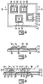
Fig. 1 is a schematic top view illustrating a foil laminated on a substrate. -
Fig. 2 is a schematic top view illustrating a conductive layer formed on the dielectric of a foil. -
Fig. 3 is a schematic cross-sectional side view taken along line 3-3 ofFig.2 . -
Fig. 4 is a schematic top view illustrating additional layers. -
Fig. 5 is a schematic cross-sectional side view taken along line 5-5 ofFig. 4 . -
Fig. 6 is a schematic cross-sectional side view of an example not part of the present invention. -
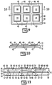
Fig. 7 is a schematic top view of a foil laminated to a substrate of the present invention with isolation dams coated thereon. -
Fig. 8 is a schematic cross-sectional side view taken along line 8-8 ofFig. 7 . -
Fig. 9 is a schematic top view of an embodiment of the present invention. -
Fig. 10 is a schematic cross-sectional side view taken along line 10-10 ofFig. 9 . -
Fig. 11 is a cross-sectional side view of an embodiment of the present invention. -
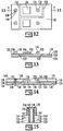
Fig. 12 is a schematic top view of an example not part of the present invention. -
Fig. 13 is a cross-sectional side view taken along line 13-13 ofFig. 12 . -
Fig. 14 is a cross-sectional side view of an example not part of the present invention. -
Fig. 15 is a cross-sectional side view of an example not part of the present invention. - The invention will be described with reference to the
figures 7-11 . Examples not part of the invention form an integral non-limiting part of the disclosure facilitating understanding of the present invention. In the various figures, similar elements will be numbered accordingly. - Described is a process for forming a capacitor which is integral to a printed circuit board or substrate. More specifically, the invention describes a process for manufacturing a printed circuit board, or substrate, with capacitance integral thereto.
- In a preferred embodiment, the substrate, with an integral capacitor, will be further processed by the incorporation of additional layers to form a completed substrate with a capacitor embedded therein.
- An example not part of the present invention can be described by the process illustrated in the following figures. In
Fig. 1 , a conductive foil, 12, is attached, adhered, or laminated to an unfinished substrate, 10. The conductive foil comprises a dielectric layer, 13, formed on at least that surface which is away from the substrate. The dielectric layer can be formed after the foil is on the substrate but prior formation is preferred. The conductive foil is preferably a valve metal selected from aluminum, tantalum, niobium, titanium or a combination thereof or a conductive oxide such as NbO. The conductive foil will ultimately form the anode. In one example, the dielectric is preferably formed by anodic oxidation of the foil. It is preferable to have only one dielectric layer; however, both sides of the foil can contain an oxide layer. Metal foil with a single oxide layer is not commercially available under favorable terms, thereby necessitating the use of a foil with both sides oxidized. It is preferred that the surface of the conductive foil is roughened to increase the surface area prior to anodizing to form the oxide dielectric. - The dielectric can be formed by other methods including vapor deposition, sol-gel applications, and solvent based applications, and may be an oxide of the conductive foil or a different material, such as a ceramic dielectric.
- As illustrated schematically in top view in
Fig. 2 and in side view inFig. 3 taken along line 3-3 ofFig. 2 , a solid electrolyte layer, 14, is formed on the exposed dielectric layer, 13, in regions where the capacitive functionality is desired. The solid electrolyte layer may consist of one or more layers of one or more conductive polymers. Preferred conductive polymers include polypyrrole, polyaniline, and polythiophene. For the purposes of the present example, polypyrrole, polyaniline, and polythiophene refer equally to derivatives thereof. The conductive polymer may be applied from a solution or suspension or the conductive polymer may be formed in-situ by coating a monomer and oxidizer sequentially. In-situ polymer formation from monomer is less preferred due to the complexities of incorporating the process into conventional in-line automated processes since the number of process steps is necessarily increased with in-situ formation. Furthermore, in-situ polymer formation from monomer typically provides a thicker, less dense, polymer layer which is less desirable in most applications. The polymer layer is applied by any technique available in the art, without limit, with exemplary methods including ink jet printing, screen-printing, gravure coating, or masked spraying. The solid electrolyte layer may comprise a manganese dioxide layer either in addition to a polymer layer or instead of the polymer layer. The manganese dioxide layer is preferably formed by applying a solution of a manganese compound, such as manganese nitrate or a permanganate, followed by converting the manganese compound to manganese dioxide by heat. It is preferable that the manganese dioxide layer be deposited prior to deposition of the polymer; however, they can be added as a mixture. - A carbon layer, 16, is preferably applied over the solid electrolyte layer, 14, as illustrated schematically in top view in
Fig. 4 and in schematic cross-sectional view inFig. 5 taken along line 5-5 ofFig. 4 . The carbon layer improves adhesion between the solid electrolyte layer, 14, and subsequent conductive layer, 18, and is therefore preferred. The carbon layer is formed on the patterned surface of the solid electrolyte layer by applying a paste, or thick ink, containing carbon particles preferably in the form of graphite or carbon black. The carbon layer can be applied by ink jet printing, screen-printing, gravure printing or by spraying without limit thereto. - The conductive layer, 18, is a layer which allows formation of a highly conductive connection between the cathode and subsequent circuitry. The conductive layer may be silver, copper, gold, or another highly conductive metal or a combination thereof. Particularly preferred is a silver, copper or silver/copper ink or paste. The layer may be deposited by ink jet printing, screen printing, gravure printing, spraying, sputtering, atomic layer deposition or other means for applying a thin layer deposition. The cathode refers to either the solid electrolyte layer or the combination of the solid electrolyte layer, carbon layer and conductive layer.
- Referring still to
Figs. 4 and 5 , each capacitive couple is preferably isolated from the others by a demarcation, 20, in the foil, which electrically isolates that portion of the foil acting as the anode and forming a capacitor with the cathode layers from the remaining foil. The demarcation can be formed by etching or dicing at least through the oxide layer and the valve metal foil layer. It would be apparent that that the kerf width of the demarcation must be sufficiently wide to avoid current crossing the demarcation. While the demarcation is illustrated as a narrow strip, it is understood that it may include any or all of the foil which is not functioning as the anode of a capacitor with the understanding that a sufficient area of foil is removed to avoid current flow from the anode portion to surrounding functioning foil. A width of about 0.025 mm is sufficient. However, 0.05 mm is more preferable. In one example, foil may remain in the finished substrate, wherein the remaining foil provides either no electrical function or functions as a component in an element other than a capacitor. In another example, windows and holes may be created in the foil base before application of the foil to the semi-finished substrate, or these areas may be removed subsequent to the application. The holes or windows will allow vias and plated through holes to pass through this layer without connection to any of the capacitive elements and will facilitate registration of the foil during the lamination process. - In one example, the conductive foil may remain intact between capacitors, thereby ultimately forming multiple capacitors with a common anode. Ground and power connections could then be established between at least two of the multiple cathodes without connecting to the conductive foil anode, comprising a capacitor device connected in a non-polar configuration. This could allow greater flexibility in the design of a circuit substrate in that an embedded capacitance layer with a given isolation dam and cathode application pattern could be utilized for more than one circuit substrate design. In one example the isolation dam is a non- conductive region formed by treating the conductive material to render it non- conductive.
- After demarcation, a functional capacitor, or multiple capacitors, is provided on a substrate and the substrate may be suitable for use in some applications. Alternatively, the demarcations may completely sever one or more junctional capacitors mounted on a substrate from the larger substrate for use. In a particularly preferred example further processing ensues to prepare a printed circuit board with capacitance incorporated therein.
- As illustrated in
Fig. 6 , it is preferable to apply, preferably by lamination, additional circuit board material, 21, over the capacitor and semi-finished substrate, thereby forming the embedded capacitance or an embedded capacitor within the substrate material. The additional circuit board layers are applied by any technique known in the art and standard materials are suitable for use therein. After lamination, and in the course of forming additional layers of the circuit board material, the anode and cathode terminals of the capacitor must be accessed for connection to eventual circuit traces on the circuit board. The connectivity among layers is preferably made with a blind via or a through hole, both of which will be described, while traces of conductive material (i.e. copper) afford connection to multiple areas at each layer. InFig. 6 , a cathodic blind via, 22, is formed directly above the cathode region of the capacitor. This allows a conductor to be brought into electrical contact with both the cathode and a cathodic circuit trace, 24, which may be at least temporarily on the surface of the circuit substrate. An anodic blind via, 26, is formed which is in electrical contact with the conductive foil forming the anode interior to the demarcation relative to the capacitive couple. The anodic blind via allows a conductor therein to form an electrical contact between the anode and an anode circuit trace, 28. An anodic through via, 30, passing through the entire substrate, is in electrical contact with the anode interior to the demarcation relative to the capacitive couple and is then in electrical contact with at least one anodic trace, 32, on a surface of the circuit substrate. It would be apparent that additional laminations may occur such that the traces described are ultimately interior to a layered circuit board. - An embodiment of the present invention will be described with reference to
Figs. 7-11 . In the Figs., the substrate, 10, foil, 12, and dielectric, 13, are as described above. An isolation dam, 40, is formed on the surface of the dielectric. In one embodiment, the interior area of the dam is the shape and size of the intended cathode and the isolation dam circumvents the cathode. The isolation dam prior to formation of a cathode is illustrated in top schematic view inFig. 7 and cross-sectional schematic view inFig. 8 taken along line 8-8 ofFig. 7 . A solid electrolyte and optional but preferred carbon and conductive layers are formed within the area of the isolation dam to form the cathode of a capacitor. The resulting capacitor is illustrated in top schematic view inFig. 9 and in schematic cross-sectional view inFig. 10 taken along line 10-10 ofFig. 9 . The isolation dam, 40, forms a pool within which the cathode, 42, is coated. After formation of the cathode, an optional but preferred metal layer, 44, is formed and the capacitors are singulated. In one embodiment, the substrate is diced along a line, 46, to isolate one or more discrete capacitor(s) on a substrate. Alternatively, the line, 46, represents a demarcation line wherein the conductive foil is interrupted between capacitors to electrically isolate discrete capacitors on a common substrate or to form discrete capacitors with a common anode. As mentioned previously, the demarcation can represent a narrow band which is sufficiently wide for electrical isolation, or a portion, up to the entire foil not otherwise functioning as the anode of a capacitor, can be removed. - A particularly preferred embodiment is illustrated schematically after further processing in
Fig. 11 . Shown therein is additional circuit board material, 41, laminated over the capacitor. As would be apparent, electrical connectivity must be made between the capacitor and traces for the function of the capacitor to be realized in an electrical circuit. Illustrated inFig. 11 are blind vias, 48, primarily for the cathodic couple, wherein the cathode is in electrical contact with a cathode trace, 50. Through vias, 52, are preferably formed through the isolation dam, 40, such that the isolation dam forms a sleeve with the through via therein. A conductor dispensed in the through via forms an electrical connection between the conductive foil, which functions as the anode, and an anode trace, 54, on at least one side of the laminated device. It would be apparent from the figure that a blind via through the isolation dam could also be utilized, wherein the blind via does not pass entirely through the structure but only through to the extent necessary to be in electrical contact with the conductive foil anode. - An example is illustrated in schematic top view in
Fig. 12 and schematic cross-sectional view inFig. 13 taken along line 13-13 ofFig. 12 . InFigs. 12 and 13 , a substrate, 126, has a foil laminated thereon. The foil comprises a first conductive layer, 128, such as a metal foil, and dielectric, 130. A cathode comprising a solid electrolyte, 134, and a second conductive layer, 136, is formed on the dielectric, such that the cathode and foil form a capacitive couple with the dielectric therebetween. The capacitive couple is isolated electrically by demarcations, 132. An isolation dam, 122, provides a via location for connection to the anode which is isolated from the remaining foil by the demarcation. A second isolation dam, 138, is provided wherein a through hole, 238, is ultimately formed for additional functionality. - An additional example is illustrated in schematic cross-sectional side view in
Fig. 14 . InFig. 14 , the substrate, 126, first conductive layer, 128, dielectric, 130, demarcation, 132, solid electrolyte layer, 134, isolation dam, 122, and second isolation dam, 138, are as described with reference toFigs. 12 and 13 . InFig. 14 , additional lamination, 140, has been added to encase the capacitor elements, thereby forming a laminated substrate with embedded capacitance. An anodic via, 144, illustrated as a blind via, is in the first isolation dam, 122. A second via, 142, illustrated as a through via, is formed in the second isolation dam, 138. The second via can be utilized to form electrical connectivity with the foil which may, or may not, be utilized in the capacitance functionality of the substrate. - Yet another example is illustrated in cross-sectional side view in
Fig. 15 . InFig. 15 , a substrate, 150, has a metal foil, 152 and 154, coated thereon, wherein the metal foil has a conductive metal, 152, and a dielectric, 154. An isolation dam, 156, is applied on the dielectric. A via, 156, preferably a through via, is formed through the isolation dam, 162, wherein the via is larger than ultimately desired. The via is preferably coated with a dielectric, 170. The via is then redrilled and filled with a conductive material, 160, The via is reformed with a smaller size than the previous via thereby forming a second via. The result is a via, 158, with a collar therein. The material can be a conductive material, such as copper, thereby forming a through via with a conductive sleeve therein. Alternatively, the material, 160, can be an insulator material thereby forming an insulative collar. - A particular feature of the present disclosure is the ability to form a capacitor with thin layers which would otherwise be difficult to manufacture. Capacitive elements with a thickness of less than 250 µm as measured from the cathode face to the opposing anode face can easily be formed with the present invention. The ability to manufacture a capacitor with thin active layers increases the capacitive volume which is an ongoing desire in capacitor manufacture. The present invention allows for the manufacture of a capacitor, being the anode, dielectric and cathode, of about 10 µm to about 250 µm thick. More preferably, the present invention allows for the manufacture of capacitors which are less than 100 µm and more preferably less than 50 µm.
- The printed circuit layers may be formed of commonly used printed circuit board materials such as FR-4, but the present invention is compatible with most available multi-layer printed circuit materials.
- In one embodiment, each subsequent layer is slightly smaller than the previous layer such that the surface projection of each layer leaves a frame from the previous layer in a "wedding cake" arrangement. This is preferred for manufacturing simplicity since it would be extremely difficult to coat a subsequent layer with the exact area of the underlying area without some material dripping down the edge of the stacked layers. Obviously, it is desirable to have as much surface area of capacitance as possible without sacrificing losses due to a subsequent layer not being isolated to the surface.
- The substrate is not particularly limited for demonstrating the invention. Particularly suitable substrates include copper, copper-coated circuit substrates such as FR-4., polyimide, phenolic, BT, and various Rogers high performance materials such as TMM, etc. Glass reinforced polymer is a particularly preferred substrate.
- The terms anode and cathode as used herein refer to the two conductive layers separated by a dielectric thereby forming a capacitive couple. For the purposes of the present invention the anode refers to the metal foil and the cathode refers to the conductive layer formed on the dielectric of the anode foil. By convention the anode is the positive terminal and the cathode is the negative terminal yet this could be reversed if contained within the lowered stress limit, without detriment and without departing from the meets and bounds of the instant invention.
- The isolation dam is a non-conductive material capable of being applied to a surface and forming a raised barrier thereon. The material is preferably applied as a thixotropic material. Particularly preferred isolation dam materials include polyimides, silicones, and epoxies.
- In the present invention, through vias and through holes are defined as vias which go through all layers in place at the time of via formation. A blind via is a via which goes through less than all of the layers in place at the time of via formation.
- Dice cutting, as used herein, refers to a cutting operation which separates discrete capacitors from the carrier or from each other and may be a complete severing or only be partially through the device. Exemplary methods include routing, saw dicing, blade dicing, water jet cutting, laser cutting, chemical etching, selective heating, laser ablation and the like.
- The foil is laminated to the substrate preferably using an adhesive. Particular preferred adhesives include polyimides, epoxies, and acrylates.
- The invention has been described with particular reference to the preferred embodiments without limit thereto. One of skill in the art would realize additional embodiments which are not specifically recited but within the scope of the claims appended hereto.
Claims (21)
- A process for forming a laminate with capacitance, comprising:providing a substrate (10);applying a conductive foil anode (12) to said substrate (10);forming a dielectric (13) on said conductive foil (12);forming a first isolation dam (40) on at least one region of said dielectric (13);forming a layer of solid electrolyte consisting of a conductive polymer or manganese dioxide that is applied from a solution or suspension and optionally carbon and conductive metal layers on at least one region of said dielectric (13) wherein said first isolation dam (40) circumvents said layer of solid electrolyte to form a cathode region; andtreating said conductive foil (12) to electrically isolate a region of said conductive foil (12) containing said layer of solid electrolyte from additional conductive foil (12) forming the anode.
- The process for forming a laminate of claim 1 wherein treating said conductive foil comprises a method selected from chemical reaction, selective heating, and laser ablation.
- The process for forming a laminate of claim 1 wherein said conductive polymeric material comprises a material selected from polypyrrole, polyaniline, and polythiophene.
- The process for forming a laminate of any of Claims 1-3 further comprising the step
of removing at least one region of said conductive foil (12) not comprising said cathode region. - The process for forming a laminate of claim 4 wherein said at least one region of said conductive foil (12) is removed prior to applying said conductive foil (12) to said substrate (10).
- The process for forming a laminate of any of claims 1-5 further comprising laminating a second substrate over said layer of solid electrolyte.
- The process for forming a laminate of claim 6 further comprising forming at least one plated through hole.
- The process for forming a laminate of any of claims 1-7 further comprising the step of forming an electrical connection between said anode region of said at least one region of said conductive foil (12) and a conductive trace.
- The process for forming a laminate of any of claims 1-8 further comprising the step of forming an electrical connection between said at least one cathode region and a conductive trace.
- The process for forming a laminate of any of claims 8 or 9, wherein said electrical connection to said conductive trace comprises a via.
- The process for forming a laminate of any of claims 1-10 1 wherein said conductive foil (12) comprises one conductor selected from aluminum, tantalum, niobium, titanium and NbO.
- The process for forming a laminate of any of claims 1-11 wherein said dielectric (13) is an oxide of said conductive foil (12).
- The process for forming a laminate of any of claims 1-12 wherein said treating said conductive foil (12) is selected from routing, saw dicing, blade dicing, chemical etching, water jet cutting and laser cutting.
- The process for forming a laminate of any of claims 1-13 wherein said substrate (10) comprises a glass-reinforced polymer.
- A laminate with capacitance, comprising:
a substrate (10); wherein the capacitance is made of:a conductive foil (12) laminated to said first substrate (10)a dielectric (13) formed on said conductive foil (12);a first isolation dam (40) formed on at least a region of said dielectric (13);a layer of solid electrolyte formed on at least a region of said dielectric (13) used as a cathode (42), consisting of a conductive polymer or manganese dioxide and optionally carbon and conductive metal layers (44);an additional circuit board material (41) laminated over said capacitance;a first trace (50) on the top surface of said additional circuit board material (41);a first via (48) forming an electrical connection between said cathode (42) and said first trace (50);a second trace (54, 54') on said substrate's (10) surface opposite to the one on which said conductive foil (12) was formed, and/or the top surface of said additional circuit board material (41); anda second via (52) forming an electrical connection between said conductive foil (12) and said second trace (54, 54'), wherein said isolation dam (40) circumvents said cathode. - The laminate with capacitance of claim 15 wherein a via or plated through hole passes through said isolation dam (40).
- The laminate with capacitance of claim 15 wherein said conductive polymeric material comprises at least one material selected from the group consisting of polypyrrole, polyaniline and polythiophene.
- The laminate with capacitance of claim 15 wherein said conductive foil (12) comprises one material selected from aluminum, tantalum, niobium, titanium and NbO.
- The laminate with capacitance of claim 18 wherein said dielectric (13) comprises at least dielectric oxide selected from aluminum, tantalum, titanium and niobium.
- The laminate with capacitance of claim 15 wherein said substrate (10) comprises a glass reinforced polymer.
- A capacitor formed by the method of any of claims 1-14 and comprising the laminate with capacitance of claim 16.
Applications Claiming Priority (2)
| Application Number | Priority Date | Filing Date | Title |
|---|---|---|---|
| US12/180,768 US8470680B2 (en) | 2008-07-28 | 2008-07-28 | Substrate with embedded patterned capacitance |
| PCT/US2009/051919 WO2010014580A2 (en) | 2008-07-28 | 2009-07-28 | Substrate with embedded patterned capacitance |
Publications (3)
| Publication Number | Publication Date |
|---|---|
| EP2313900A2 EP2313900A2 (en) | 2011-04-27 |
| EP2313900A4 EP2313900A4 (en) | 2011-12-28 |
| EP2313900B1 true EP2313900B1 (en) | 2021-03-24 |
Family
ID=41568451
Family Applications (1)
| Application Number | Title | Priority Date | Filing Date |
|---|---|---|---|
| EP09803461.4A Active EP2313900B1 (en) | 2008-07-28 | 2009-07-28 | Substrate with embedded patterned capacitance |
Country Status (4)
| Country | Link |
|---|---|
| US (3) | US8470680B2 (en) |
| EP (1) | EP2313900B1 (en) |
| CN (1) | CN102105955A (en) |
| WO (1) | WO2010014580A2 (en) |
Families Citing this family (14)
| Publication number | Priority date | Publication date | Assignee | Title |
|---|---|---|---|---|
| US8568456B2 (en) | 2009-09-21 | 2013-10-29 | Globus Medical, Inc. | Transverse connector having a locking element for capturing multiple rods |
| US9123780B2 (en) * | 2012-12-19 | 2015-09-01 | Invensas Corporation | Method and structures for heat dissipating interposers |
| WO2014127221A1 (en) | 2013-02-14 | 2014-08-21 | Kemet Electronics Corporation | Capacitor array and method of manufacturing |
| US9558390B2 (en) * | 2014-07-25 | 2017-01-31 | Qualcomm Incorporated | High-resolution electric field sensor in cover glass |
| TWI546834B (en) * | 2014-10-28 | 2016-08-21 | 鈺邦科技股份有限公司 | Chip solid electrolytic capacitor and manufacturing method thereof |
| US9767962B2 (en) | 2016-01-22 | 2017-09-19 | Micron Technology, Inc. | Apparatuses, multi-chip modules and capacitive chips |
| US10978403B2 (en) | 2019-01-30 | 2021-04-13 | Delta Electronics, Inc. | Package structure and method for fabricating the same |
| WO2018236784A1 (en) * | 2017-06-19 | 2018-12-27 | Industrial Heat, Llc | Exothermic reaction electrode structure using pcb and semiconductor fabrication methods |
| US11943869B2 (en) | 2020-02-04 | 2024-03-26 | Kemet Electronics Corporation | Electrically functional circuit board core material |
| WO2021158879A1 (en) * | 2020-02-06 | 2021-08-12 | Novelis Inc. | Planar high-density aluminum capacitors for stacking and embedding |
| US11631549B2 (en) | 2020-07-30 | 2023-04-18 | Medtronic, Inc. | Electrical component and method of forming same |
| US11756741B2 (en) * | 2020-07-30 | 2023-09-12 | Medtronic, Inc. | Electrical component and method of forming same |
| US12070609B2 (en) | 2020-07-30 | 2024-08-27 | Medtronic, Inc. | Electrical component and method of forming same |
| JP7683684B2 (en) * | 2021-05-10 | 2025-05-27 | 株式会社村田製作所 | Semiconductor device and module |
Family Cites Families (24)
| Publication number | Priority date | Publication date | Assignee | Title |
|---|---|---|---|---|
| US182781A (en) * | 1876-10-03 | Improvement in steam-heaters | ||
| NL7413380A (en) | 1974-10-11 | 1976-04-13 | Philips Nv | PROCESS FOR THE MANUFACTURE OF SOLID CONDENSERS. |
| US5968210A (en) * | 1997-11-12 | 1999-10-19 | Pacesetter, Inc. | Electrolytic capacitor and method of manufacture |
| US6865071B2 (en) * | 1998-03-03 | 2005-03-08 | Acktar Ltd. | Electrolytic capacitors and method for making them |
| JP2001210789A (en) | 2000-01-21 | 2001-08-03 | Hitachi Ltd | Electronic circuit with built-in thin film capacitor and method of manufacturing the same |
| US6628505B1 (en) * | 2000-07-29 | 2003-09-30 | Biosource, Inc. | Flow-through capacitor, system and method |
| US6657849B1 (en) * | 2000-08-24 | 2003-12-02 | Oak-Mitsui, Inc. | Formation of an embedded capacitor plane using a thin dielectric |
| US6571126B1 (en) * | 2000-11-03 | 2003-05-27 | Cardiac Pacemakers, Inc. | Method of constructing a capacitor stack for a flat capacitor |
| US6462935B1 (en) * | 2001-09-07 | 2002-10-08 | Lih-Ren Shiue | Replaceable flow-through capacitors for removing charged species from liquids |
| US6852137B2 (en) | 2001-07-17 | 2005-02-08 | Matsushita Electric Industrial Co., Ltd. | Method for manufacturing solid electrolytic capacitor |
| JP2004128333A (en) * | 2002-10-04 | 2004-04-22 | Shinko Electric Ind Co Ltd | Thin film capacitor device, its mounting module and manufacturing method |
| EP1434242B1 (en) * | 2002-12-27 | 2010-11-24 | Panasonic Corporation | Capacitor and method for producing the same, and circuit board with a built-in capacitor and method for producing the same |
| JP4647194B2 (en) * | 2003-07-14 | 2011-03-09 | 新光電気工業株式会社 | Capacitor device and manufacturing method thereof |
| US7193838B2 (en) * | 2003-12-23 | 2007-03-20 | Motorola, Inc. | Printed circuit dielectric foil and embedded capacitors |
| US7100277B2 (en) * | 2004-07-01 | 2006-09-05 | E. I. Du Pont De Nemours And Company | Methods of forming printed circuit boards having embedded thick film capacitors |
| JP2006040938A (en) * | 2004-07-22 | 2006-02-09 | Nec Tokin Corp | Solid electrolytic capacitor, laminated capacitor using the same and its manufacturing method |
| JP2006147606A (en) * | 2004-11-16 | 2006-06-08 | Nec Toppan Circuit Solutions Inc | Sheet capacitor and manufacturing method thereof |
| US7138068B2 (en) * | 2005-03-21 | 2006-11-21 | Motorola, Inc. | Printed circuit patterned embedded capacitance layer |
| US7741189B2 (en) * | 2005-06-20 | 2010-06-22 | E.I. Du Pont De Nemours And Company | Electrodes, inner layers, capacitors, electronic devices and methods of making thereof |
| JP4508193B2 (en) | 2005-07-13 | 2010-07-21 | パナソニック株式会社 | Mounting board, mounting body and electronic device using the same |
| KR100714580B1 (en) * | 2005-11-03 | 2007-05-07 | 삼성전기주식회사 | Method for manufacturing printed circuit board with thin film capacitor and printed circuit board manufactured therefrom |
| KR100691621B1 (en) * | 2006-02-01 | 2007-03-12 | 삼성전기주식회사 | Manufacturing method of printed circuit board with thin film capacitor |
| JP4738299B2 (en) * | 2006-09-20 | 2011-08-03 | 富士通株式会社 | Capacitor, manufacturing method thereof, and electronic substrate |
| US7745281B2 (en) * | 2007-03-07 | 2010-06-29 | Kemet Electronics Corporation | Thin solid electrolytic capacitor embeddable in a substrate |
-
2008
- 2008-07-28 US US12/180,768 patent/US8470680B2/en active Active
-
2009
- 2009-07-28 EP EP09803461.4A patent/EP2313900B1/en active Active
- 2009-07-28 CN CN2009801293685A patent/CN102105955A/en active Pending
- 2009-07-28 WO PCT/US2009/051919 patent/WO2010014580A2/en not_active Ceased
-
2012
- 2012-01-06 US US13/345,227 patent/US8410536B2/en active Active
- 2012-03-01 US US13/409,424 patent/US8652920B2/en active Active
Non-Patent Citations (1)
| Title |
|---|
| None * |
Also Published As
| Publication number | Publication date |
|---|---|
| US20120162857A1 (en) | 2012-06-28 |
| US8410536B2 (en) | 2013-04-02 |
| US20120106032A1 (en) | 2012-05-03 |
| US8652920B2 (en) | 2014-02-18 |
| EP2313900A4 (en) | 2011-12-28 |
| CN102105955A (en) | 2011-06-22 |
| US20100020473A1 (en) | 2010-01-28 |
| WO2010014580A3 (en) | 2010-04-15 |
| US8470680B2 (en) | 2013-06-25 |
| WO2010014580A2 (en) | 2010-02-04 |
| EP2313900A2 (en) | 2011-04-27 |
Similar Documents
| Publication | Publication Date | Title |
|---|---|---|
| US8652920B2 (en) | Substrate with embedded patterned capacitance | |
| JP4479050B2 (en) | Solid electrolytic capacitor | |
| JP4432207B2 (en) | Capacitor | |
| KR100584803B1 (en) | High tolerance embedded capacitors | |
| JP2013243392A (en) | Method for forming electric device including thin solid electrolytic capacitor embeddable in substrate | |
| JP2006040938A (en) | Solid electrolytic capacitor, laminated capacitor using the same and its manufacturing method | |
| US6855177B2 (en) | Method for producing solid electrolytic capacitor | |
| EP1372168A1 (en) | Solid electrolytic capacitor and method of manufacturing the capacitor | |
| JP2005045068A (en) | Solid electrolytic capacitor | |
| US6794260B2 (en) | Method of manufacturing solid-state electrolytic capacitor | |
| JP2006510233A (en) | Printed wiring board having low-inductance embedded capacitor and manufacturing method thereof | |
| EP1310966B1 (en) | Composite electronic components | |
| US7508652B2 (en) | Solid electrolytic capacitor and method of making same | |
| TWI294133B (en) | Thick-film capacitors, embedding thick-film capacitors inside printed circuit boards, and methods of forming such capacitors and printed circuit boards | |
| JP4747569B2 (en) | Manufacturing method of substrate with built-in solid electrolytic capacitor | |
| US7833292B2 (en) | Channel method for forming a capacitor | |
| JP4599653B2 (en) | Sheet capacitor | |
| JP2008098487A (en) | Solid electrolytic capacitor, solid electrolytic capacitor built-in substrate, and manufacturing method thereof | |
| JP4337423B2 (en) | Circuit module | |
| JP4831240B2 (en) | Manufacturing method of sheet capacitor | |
| JP2008085083A (en) | Capacitor manufacturing method | |
| JPH0693421B2 (en) | Method for manufacturing solid electrolytic capacitor | |
| JP2003031438A (en) | Method for manufacturing solid electrolytic capacitor | |
| JP2002289471A (en) | Solid electrolytic capacitors |
Legal Events
| Date | Code | Title | Description |
|---|---|---|---|
| PUAI | Public reference made under article 153(3) epc to a published international application that has entered the european phase |
Free format text: ORIGINAL CODE: 0009012 |
|
| 17P | Request for examination filed |
Effective date: 20110214 |
|
| AK | Designated contracting states |
Kind code of ref document: A2 Designated state(s): AT BE BG CH CY CZ DE DK EE ES FI FR GB GR HR HU IE IS IT LI LT LU LV MC MK MT NL NO PL PT RO SE SI SK SM TR |
|
| AX | Request for extension of the european patent |
Extension state: AL BA RS |
|
| RIN1 | Information on inventor provided before grant (corrected) |
Inventor name: DUNN, GREGORY, J. Inventor name: CHACKO, ANTONY, P. Inventor name: MELODY, ALETHIA Inventor name: STOLARSKI, CHRIS Inventor name: PRYMAK, JOHN, D. |
|
| RIN1 | Information on inventor provided before grant (corrected) |
Inventor name: DUNN, GREGORY, J. Inventor name: CHACKO, ANTONY, P. Inventor name: MELODY, ALETHIA Inventor name: STOLARSKI, CHRIS Inventor name: PRYMAK, JOHN, D. |
|
| DAX | Request for extension of the european patent (deleted) | ||
| A4 | Supplementary search report drawn up and despatched |
Effective date: 20111124 |
|
| RIC1 | Information provided on ipc code assigned before grant |
Ipc: H05K 1/16 20060101ALI20111118BHEP Ipc: H01G 4/12 20060101ALI20111118BHEP Ipc: H01G 4/40 20060101AFI20111118BHEP |
|
| 17Q | First examination report despatched |
Effective date: 20121106 |
|
| STAA | Information on the status of an ep patent application or granted ep patent |
Free format text: STATUS: EXAMINATION IS IN PROGRESS |
|
| GRAP | Despatch of communication of intention to grant a patent |
Free format text: ORIGINAL CODE: EPIDOSNIGR1 |
|
| STAA | Information on the status of an ep patent application or granted ep patent |
Free format text: STATUS: GRANT OF PATENT IS INTENDED |
|
| INTG | Intention to grant announced |
Effective date: 20201112 |
|
| GRAS | Grant fee paid |
Free format text: ORIGINAL CODE: EPIDOSNIGR3 |
|
| GRAA | (expected) grant |
Free format text: ORIGINAL CODE: 0009210 |
|
| STAA | Information on the status of an ep patent application or granted ep patent |
Free format text: STATUS: THE PATENT HAS BEEN GRANTED |
|
| AK | Designated contracting states |
Kind code of ref document: B1 Designated state(s): AT BE BG CH CY CZ DE DK EE ES FI FR GB GR HR HU IE IS IT LI LT LU LV MC MK MT NL NO PL PT RO SE SI SK SM TR |
|
| REG | Reference to a national code |
Ref country code: GB Ref legal event code: FG4D |
|
| REG | Reference to a national code |
Ref country code: CH Ref legal event code: EP |
|
| REG | Reference to a national code |
Ref country code: IE Ref legal event code: FG4D |
|
| REG | Reference to a national code |
Ref country code: AT Ref legal event code: REF Ref document number: 1375330 Country of ref document: AT Kind code of ref document: T Effective date: 20210415 Ref country code: DE Ref legal event code: R096 Ref document number: 602009063501 Country of ref document: DE |
|
| REG | Reference to a national code |
Ref country code: LT Ref legal event code: MG9D |
|
| PG25 | Lapsed in a contracting state [announced via postgrant information from national office to epo] |
Ref country code: BG Free format text: LAPSE BECAUSE OF FAILURE TO SUBMIT A TRANSLATION OF THE DESCRIPTION OR TO PAY THE FEE WITHIN THE PRESCRIBED TIME-LIMIT Effective date: 20210624 Ref country code: NO Free format text: LAPSE BECAUSE OF FAILURE TO SUBMIT A TRANSLATION OF THE DESCRIPTION OR TO PAY THE FEE WITHIN THE PRESCRIBED TIME-LIMIT Effective date: 20210624 Ref country code: HR Free format text: LAPSE BECAUSE OF FAILURE TO SUBMIT A TRANSLATION OF THE DESCRIPTION OR TO PAY THE FEE WITHIN THE PRESCRIBED TIME-LIMIT Effective date: 20210324 Ref country code: GR Free format text: LAPSE BECAUSE OF FAILURE TO SUBMIT A TRANSLATION OF THE DESCRIPTION OR TO PAY THE FEE WITHIN THE PRESCRIBED TIME-LIMIT Effective date: 20210625 Ref country code: FI Free format text: LAPSE BECAUSE OF FAILURE TO SUBMIT A TRANSLATION OF THE DESCRIPTION OR TO PAY THE FEE WITHIN THE PRESCRIBED TIME-LIMIT Effective date: 20210324 |
|
| PG25 | Lapsed in a contracting state [announced via postgrant information from national office to epo] |
Ref country code: SE Free format text: LAPSE BECAUSE OF FAILURE TO SUBMIT A TRANSLATION OF THE DESCRIPTION OR TO PAY THE FEE WITHIN THE PRESCRIBED TIME-LIMIT Effective date: 20210324 Ref country code: LV Free format text: LAPSE BECAUSE OF FAILURE TO SUBMIT A TRANSLATION OF THE DESCRIPTION OR TO PAY THE FEE WITHIN THE PRESCRIBED TIME-LIMIT Effective date: 20210324 |
|
| REG | Reference to a national code |
Ref country code: NL Ref legal event code: MP Effective date: 20210324 |
|
| REG | Reference to a national code |
Ref country code: AT Ref legal event code: MK05 Ref document number: 1375330 Country of ref document: AT Kind code of ref document: T Effective date: 20210324 |
|
| PG25 | Lapsed in a contracting state [announced via postgrant information from national office to epo] |
Ref country code: NL Free format text: LAPSE BECAUSE OF FAILURE TO SUBMIT A TRANSLATION OF THE DESCRIPTION OR TO PAY THE FEE WITHIN THE PRESCRIBED TIME-LIMIT Effective date: 20210324 |
|
| PG25 | Lapsed in a contracting state [announced via postgrant information from national office to epo] |
Ref country code: LT Free format text: LAPSE BECAUSE OF FAILURE TO SUBMIT A TRANSLATION OF THE DESCRIPTION OR TO PAY THE FEE WITHIN THE PRESCRIBED TIME-LIMIT Effective date: 20210324 Ref country code: EE Free format text: LAPSE BECAUSE OF FAILURE TO SUBMIT A TRANSLATION OF THE DESCRIPTION OR TO PAY THE FEE WITHIN THE PRESCRIBED TIME-LIMIT Effective date: 20210324 Ref country code: CZ Free format text: LAPSE BECAUSE OF FAILURE TO SUBMIT A TRANSLATION OF THE DESCRIPTION OR TO PAY THE FEE WITHIN THE PRESCRIBED TIME-LIMIT Effective date: 20210324 Ref country code: AT Free format text: LAPSE BECAUSE OF FAILURE TO SUBMIT A TRANSLATION OF THE DESCRIPTION OR TO PAY THE FEE WITHIN THE PRESCRIBED TIME-LIMIT Effective date: 20210324 Ref country code: SM Free format text: LAPSE BECAUSE OF FAILURE TO SUBMIT A TRANSLATION OF THE DESCRIPTION OR TO PAY THE FEE WITHIN THE PRESCRIBED TIME-LIMIT Effective date: 20210324 |
|
| PG25 | Lapsed in a contracting state [announced via postgrant information from national office to epo] |
Ref country code: RO Free format text: LAPSE BECAUSE OF FAILURE TO SUBMIT A TRANSLATION OF THE DESCRIPTION OR TO PAY THE FEE WITHIN THE PRESCRIBED TIME-LIMIT Effective date: 20210324 Ref country code: IS Free format text: LAPSE BECAUSE OF FAILURE TO SUBMIT A TRANSLATION OF THE DESCRIPTION OR TO PAY THE FEE WITHIN THE PRESCRIBED TIME-LIMIT Effective date: 20210724 Ref country code: PT Free format text: LAPSE BECAUSE OF FAILURE TO SUBMIT A TRANSLATION OF THE DESCRIPTION OR TO PAY THE FEE WITHIN THE PRESCRIBED TIME-LIMIT Effective date: 20210726 Ref country code: PL Free format text: LAPSE BECAUSE OF FAILURE TO SUBMIT A TRANSLATION OF THE DESCRIPTION OR TO PAY THE FEE WITHIN THE PRESCRIBED TIME-LIMIT Effective date: 20210324 Ref country code: SK Free format text: LAPSE BECAUSE OF FAILURE TO SUBMIT A TRANSLATION OF THE DESCRIPTION OR TO PAY THE FEE WITHIN THE PRESCRIBED TIME-LIMIT Effective date: 20210324 Ref country code: ES Free format text: LAPSE BECAUSE OF FAILURE TO SUBMIT A TRANSLATION OF THE DESCRIPTION OR TO PAY THE FEE WITHIN THE PRESCRIBED TIME-LIMIT Effective date: 20210324 |
|
| REG | Reference to a national code |
Ref country code: DE Ref legal event code: R097 Ref document number: 602009063501 Country of ref document: DE |
|
| PG25 | Lapsed in a contracting state [announced via postgrant information from national office to epo] |
Ref country code: DK Free format text: LAPSE BECAUSE OF FAILURE TO SUBMIT A TRANSLATION OF THE DESCRIPTION OR TO PAY THE FEE WITHIN THE PRESCRIBED TIME-LIMIT Effective date: 20210324 |
|
| PLBE | No opposition filed within time limit |
Free format text: ORIGINAL CODE: 0009261 |
|
| STAA | Information on the status of an ep patent application or granted ep patent |
Free format text: STATUS: NO OPPOSITION FILED WITHIN TIME LIMIT |
|
| PG25 | Lapsed in a contracting state [announced via postgrant information from national office to epo] |
Ref country code: SI Free format text: LAPSE BECAUSE OF FAILURE TO SUBMIT A TRANSLATION OF THE DESCRIPTION OR TO PAY THE FEE WITHIN THE PRESCRIBED TIME-LIMIT Effective date: 20210324 |
|
| REG | Reference to a national code |
Ref country code: CH Ref legal event code: PL |
|
| 26N | No opposition filed |
Effective date: 20220104 |
|
| GBPC | Gb: european patent ceased through non-payment of renewal fee |
Effective date: 20210728 |
|
| PG25 | Lapsed in a contracting state [announced via postgrant information from national office to epo] |
Ref country code: MC Free format text: LAPSE BECAUSE OF FAILURE TO SUBMIT A TRANSLATION OF THE DESCRIPTION OR TO PAY THE FEE WITHIN THE PRESCRIBED TIME-LIMIT Effective date: 20210324 |
|
| REG | Reference to a national code |
Ref country code: BE Ref legal event code: MM Effective date: 20210731 |
|
| PG25 | Lapsed in a contracting state [announced via postgrant information from national office to epo] |
Ref country code: LI Free format text: LAPSE BECAUSE OF NON-PAYMENT OF DUE FEES Effective date: 20210731 Ref country code: GB Free format text: LAPSE BECAUSE OF NON-PAYMENT OF DUE FEES Effective date: 20210728 Ref country code: CH Free format text: LAPSE BECAUSE OF NON-PAYMENT OF DUE FEES Effective date: 20210731 |
|
| PG25 | Lapsed in a contracting state [announced via postgrant information from national office to epo] |
Ref country code: IS Free format text: LAPSE BECAUSE OF FAILURE TO SUBMIT A TRANSLATION OF THE DESCRIPTION OR TO PAY THE FEE WITHIN THE PRESCRIBED TIME-LIMIT Effective date: 20210724 Ref country code: LU Free format text: LAPSE BECAUSE OF NON-PAYMENT OF DUE FEES Effective date: 20210728 Ref country code: FR Free format text: LAPSE BECAUSE OF NON-PAYMENT OF DUE FEES Effective date: 20210731 |
|
| PG25 | Lapsed in a contracting state [announced via postgrant information from national office to epo] |
Ref country code: IE Free format text: LAPSE BECAUSE OF NON-PAYMENT OF DUE FEES Effective date: 20210728 Ref country code: BE Free format text: LAPSE BECAUSE OF NON-PAYMENT OF DUE FEES Effective date: 20210731 |
|
| PG25 | Lapsed in a contracting state [announced via postgrant information from national office to epo] |
Ref country code: IT Free format text: LAPSE BECAUSE OF FAILURE TO SUBMIT A TRANSLATION OF THE DESCRIPTION OR TO PAY THE FEE WITHIN THE PRESCRIBED TIME-LIMIT Effective date: 20210324 |
|
| PG25 | Lapsed in a contracting state [announced via postgrant information from national office to epo] |
Ref country code: HU Free format text: LAPSE BECAUSE OF FAILURE TO SUBMIT A TRANSLATION OF THE DESCRIPTION OR TO PAY THE FEE WITHIN THE PRESCRIBED TIME-LIMIT; INVALID AB INITIO Effective date: 20090728 Ref country code: CY Free format text: LAPSE BECAUSE OF FAILURE TO SUBMIT A TRANSLATION OF THE DESCRIPTION OR TO PAY THE FEE WITHIN THE PRESCRIBED TIME-LIMIT Effective date: 20210324 |
|
| P01 | Opt-out of the competence of the unified patent court (upc) registered |
Effective date: 20230427 |
|
| PG25 | Lapsed in a contracting state [announced via postgrant information from national office to epo] |
Ref country code: MK Free format text: LAPSE BECAUSE OF FAILURE TO SUBMIT A TRANSLATION OF THE DESCRIPTION OR TO PAY THE FEE WITHIN THE PRESCRIBED TIME-LIMIT Effective date: 20210324 |
|
| PG25 | Lapsed in a contracting state [announced via postgrant information from national office to epo] |
Ref country code: TR Free format text: LAPSE BECAUSE OF FAILURE TO SUBMIT A TRANSLATION OF THE DESCRIPTION OR TO PAY THE FEE WITHIN THE PRESCRIBED TIME-LIMIT Effective date: 20210324 |
|
| PG25 | Lapsed in a contracting state [announced via postgrant information from national office to epo] |
Ref country code: MT Free format text: LAPSE BECAUSE OF FAILURE TO SUBMIT A TRANSLATION OF THE DESCRIPTION OR TO PAY THE FEE WITHIN THE PRESCRIBED TIME-LIMIT Effective date: 20210324 |
|
| PGFP | Annual fee paid to national office [announced via postgrant information from national office to epo] |
Ref country code: DE Payment date: 20250604 Year of fee payment: 17 |