EP2312357A2 - Optical devices and methods of fabricating the same - Google Patents
Optical devices and methods of fabricating the same Download PDFInfo
- Publication number
- EP2312357A2 EP2312357A2 EP10152992A EP10152992A EP2312357A2 EP 2312357 A2 EP2312357 A2 EP 2312357A2 EP 10152992 A EP10152992 A EP 10152992A EP 10152992 A EP10152992 A EP 10152992A EP 2312357 A2 EP2312357 A2 EP 2312357A2
- Authority
- EP
- European Patent Office
- Prior art keywords
- chip
- platform
- optical active
- clad layer
- alignment mark
- Prior art date
- Legal status (The legal status is an assumption and is not a legal conclusion. Google has not performed a legal analysis and makes no representation as to the accuracy of the status listed.)
- Granted
Links
Images





Classifications
-
- H—ELECTRICITY
- H10—SEMICONDUCTOR DEVICES; ELECTRIC SOLID-STATE DEVICES NOT OTHERWISE PROVIDED FOR
- H10F—INORGANIC SEMICONDUCTOR DEVICES SENSITIVE TO INFRARED RADIATION, LIGHT, ELECTROMAGNETIC RADIATION OF SHORTER WAVELENGTH OR CORPUSCULAR RADIATION
- H10F99/00—Subject matter not provided for in other groups of this subclass
-
- G—PHYSICS
- G02—OPTICS
- G02B—OPTICAL ELEMENTS, SYSTEMS OR APPARATUS
- G02B6/00—Light guides; Structural details of arrangements comprising light guides and other optical elements, e.g. couplings
- G02B6/10—Light guides; Structural details of arrangements comprising light guides and other optical elements, e.g. couplings of the optical waveguide type
- G02B6/12—Light guides; Structural details of arrangements comprising light guides and other optical elements, e.g. couplings of the optical waveguide type of the integrated circuit kind
- G02B6/13—Integrated optical circuits characterised by the manufacturing method
- G02B6/136—Integrated optical circuits characterised by the manufacturing method by etching
-
- G—PHYSICS
- G02—OPTICS
- G02B—OPTICAL ELEMENTS, SYSTEMS OR APPARATUS
- G02B6/00—Light guides; Structural details of arrangements comprising light guides and other optical elements, e.g. couplings
- G02B6/24—Coupling light guides
- G02B6/42—Coupling light guides with opto-electronic elements
- G02B6/4201—Packages, e.g. shape, construction, internal or external details
- G02B6/4219—Mechanical fixtures for holding or positioning the elements relative to each other in the couplings; Alignment methods for the elements, e.g. measuring or observing methods especially used therefor
- G02B6/4228—Passive alignment, i.e. without a detection of the degree of coupling or the position of the elements
- G02B6/423—Passive alignment, i.e. without a detection of the degree of coupling or the position of the elements using guiding surfaces for the alignment
-
- G—PHYSICS
- G02—OPTICS
- G02B—OPTICAL ELEMENTS, SYSTEMS OR APPARATUS
- G02B6/00—Light guides; Structural details of arrangements comprising light guides and other optical elements, e.g. couplings
- G02B6/24—Coupling light guides
- G02B6/42—Coupling light guides with opto-electronic elements
- G02B6/4201—Packages, e.g. shape, construction, internal or external details
- G02B6/4219—Mechanical fixtures for holding or positioning the elements relative to each other in the couplings; Alignment methods for the elements, e.g. measuring or observing methods especially used therefor
- G02B6/4228—Passive alignment, i.e. without a detection of the degree of coupling or the position of the elements
- G02B6/423—Passive alignment, i.e. without a detection of the degree of coupling or the position of the elements using guiding surfaces for the alignment
- G02B6/4231—Passive alignment, i.e. without a detection of the degree of coupling or the position of the elements using guiding surfaces for the alignment with intermediate elements, e.g. rods and balls, between the elements
-
- H—ELECTRICITY
- H10—SEMICONDUCTOR DEVICES; ELECTRIC SOLID-STATE DEVICES NOT OTHERWISE PROVIDED FOR
- H10W—GENERIC PACKAGES, INTERCONNECTIONS, CONNECTORS OR OTHER CONSTRUCTIONAL DETAILS OF DEVICES COVERED BY CLASS H10
- H10W72/00—Interconnections or connectors in packages
- H10W72/01—Manufacture or treatment
- H10W72/012—Manufacture or treatment of bump connectors, dummy bumps or thermal bumps
-
- G—PHYSICS
- G02—OPTICS
- G02B—OPTICAL ELEMENTS, SYSTEMS OR APPARATUS
- G02B6/00—Light guides; Structural details of arrangements comprising light guides and other optical elements, e.g. couplings
- G02B6/10—Light guides; Structural details of arrangements comprising light guides and other optical elements, e.g. couplings of the optical waveguide type
- G02B6/12—Light guides; Structural details of arrangements comprising light guides and other optical elements, e.g. couplings of the optical waveguide type of the integrated circuit kind
- G02B2006/12166—Manufacturing methods
- G02B2006/12176—Etching
Definitions
- the present disclosure herein relates to optical devices and methods of fabricating the same, and more particularly, to optical devices in which an optical active chip such as a laser diode and a photodiode and a planar lightwave circuit platform having an integrated light waveguide are hybrid-coupled and methods of fabricating the same.
- an optical active chip such as a laser diode and a photodiode and a planar lightwave circuit platform having an integrated light waveguide are hybrid-coupled and methods of fabricating the same.
- an optical active device performing light source, optical detection, and optical amplification functions and a light waveguide in which optical wavelength division and optical multiplexing are possible are integrated to realize an optical transceiver and optical amplification module at a low price.
- Such integration technologies are divided into a monolithic integration technology in which an optical active device and a light waveguide are realized and integrated using an optical semiconductor that is a single material and a planar lightwave circuit (PLC) hybrid integration technology in which an optical active device and a PLC platform are integrated using a flip-chip (F/C) bonding.
- PLC planar lightwave circuit
- the PLC hybrid integration technology when each of optical devices is integrated on a single substrate, it may be difficult to realize an optical transceiver module at a low price due to limitations in optimization of the optical devices, reproducibility, and productivity.
- an optical active device having optimal performances may be hybrid-integrated with a PLC platform having a light waveguide function and a wavelength division multiplexing (WDM) filter function to improve productivity.
- WDM wavelength division multiplexing
- a PLC platform may be easily manufactured using existing light waveguide manufacturing technologies and platform post-processes such as an etching process and a metal deposition process.
- platform post-processes such as an etching process and a metal deposition process.
- Embodiments of the inventive concept provide an optical device that may improve alignment accuracy to enhance optical coupling efficiency when an optical active chip is bonded to a PLC platform.
- Embodiments of the inventive concept also provide a method of fabricating an optical device, which may improve alignment accuracy to enhance optical coupling efficiency when an optical active chip is bonded to a PLC platform.
- Embodiments of the inventive concept provide optical devices which include things as in the following: a substrate having a waveguide region and a mounting region; a planar lightwave circuit (PLC) waveguide including a lower-clad layer and an upper-clad layer on the waveguide region of the substrate and a platform core between the lower-clad layer and the upper-clad layer; a terrace defined by etching the lower-clad layer on the mounting region of the substrate, the terrace including a trench; a platform under bump metallurgy (UBM) disposed on the etched surface of the lower-clad layer around the terrace disposed on the mounting region of the substrate; an optical active chip mounted on the mounting region of the substrate and including a chip core therein; a chip UBM and a chip alignment mark disposed on a mounting surface of the optical active chip; and a solder film electrically connecting the platform UBM to the chip UBM.
- the optical active chip is aligned by interlocking between the trench of the terrace and the chip alignment mark of the optical active chip
- a distance between an inner circumference surface of the trench of the terrace and an outer circumference surface of the chip alignment mark of the optical active chip may range from about 1 ⁇ m to about 2 ⁇ m.
- the solder film may have a thickness ranging from about 2 ⁇ m to about 8 ⁇ m.
- the solder film may include an AuSn solder.
- the optical devices may further include an additional solder film disposed on the chip alignment mark.
- a distance between the PLC waveguide and the optical active chip may range from about 2.5 ⁇ m to about 20 ⁇ m.
- other optical devices include things as follows: a substrate having a waveguide region and a mounting region; a PLC waveguide including a lower-clad layer and an upper-clad layer on the waveguide region of the substrate and a platform core between the lower-clad layer and the upper-clad layer; a terrace defined by etching the lower-clad layer on the mounting region of the substrate; a platform UBM disposed on the etched surface of the lower-clad layer around the terrace disposed on the mounting region of the substrate; a platform alignment mark disposed on an upper surface of the terrace; an optical active chip mounted on the mounting region of the substrate and including a chip core therein; a chip UBM and a chip alignment mark disposed on a mounting surface of the optical active chip; and a solder film electrically connecting the platform UBM to the chip UBM.
- the optical active chip is aligned by interlocking between the platform alignment mark of the terrace and the chip alignment mark of the optical active chip and mounted on the mounting region.
- the platform alignment mark of the terrace and the chip alignment mark of the optical active chip may have intaglio and relief shapes corresponding to each other, respectively.
- a distance between the platform alignment mark of the terrace and the chip alignment mark of the optical active chip may range from about 1 ⁇ m to about 2 ⁇ m.
- the solder film may have a thickness ranging from about 2 ⁇ m to about 8 ⁇ m.
- the solder film may include an AuSn solder.
- a distance between the PLC waveguide and the optical active chip may range from about 2.5 ⁇ m to about 20 ⁇ m.
- methods of fabricating an optical device including: sequentially forming a lower-clad layer, a platform core, and an upper-clad layer on a substrate having a waveguide region and a mounting region; performing a first etch process on the upper-clad layer, the platform core, and the lower-clad layer disposed on the mounting region of the substrate to form a PLC waveguide in the waveguide region and a lower-clad layer having a first height in the mounting region; performing a second etch process on the lower-clad layer having the first height disposed on the mounting region of the substrate to form a terrace having the first height and a trench and a lower-clad layer having a second height; forming a platform UBM on the lower-clad layer having the second height around the terrace disposed on the mounting region of the substrate; forming a chip UBM on a mounting surface of the optical active chip including a chip core therein; forming a chip alignment mark on a mounting surface of an optical active chip; forming
- a distance between an inner circumference surface of the trench of the terrace and an outer circumference surface of the chip alignment mark of the optical active chip may range from about 1 ⁇ m to about 2 ⁇ m.
- the solder film may be formed on each of the platform UBM and the chip UBM.
- the solder film may have a thickness ranging from about 1 ⁇ m to about 4 ⁇ m.
- the solder film may include an AuSn solder.
- the chip UBM and the chip alignment mark may be formed at the same time.
- the optical active chip may further include an additional solder film disposed on the chip alignment mark.
- a distance between the PLC waveguide and the optical active chip may range from about 2.5 ⁇ m to about 20 ⁇ m.
- methods of fabricating another optical device including: sequentially forming a lower-clad layer, a platform core, and an upper-clad layer on a substrate having a waveguide region and a mounting region; performing a first etch process on the upper-clad layer, the platform core, and the lower-clad layer disposed on the mounting region of the substrate to form a PLC waveguide in the waveguide region and a lower-clad layer having a first height in the mounting region; performing a second etch process on the lower-clad layer having the first height disposed on the mounting region of the substrate to form a terrace having the first height and a lower-clad layer having a second height; forming a platform UBM on the lower-clad layer having the second height around the terrace disposed on the mounting region of the substrate; forming a platform alignment mark on an upper surface of the terrace disposed on the mounting region of the substrate; forming a chip UBM on a mounting surface of the optical active chip including a chip core therein;
- the platform alignment mark of the terrace and the chip alignment mark of the optical active chip may have intaglio and relief shapes corresponding to each other, respectively.
- a distance between the platform alignment mark of the terrace and the chip alignment mark of the optical active chip may range from about 1 ⁇ m to about 2 ⁇ m.
- the solder film may be formed on each of the platform UBM and the chip UBM.
- the solder film may have a thickness ranging from about 1 ⁇ m to about 4 ⁇ m.
- the solder film may include an AuSn solder.
- the platform UBM and the platform alignment mark may be formed at the same time.
- the chip UBM and the chip alignment mark may be formed at the same time.
- a distance between the PLC waveguide and the optical active chip may range from about 2.5 ⁇ m to about 20 ⁇ m.
- FIG. 1A is a plan view of an optical device according to an embodiment of the inventive concept
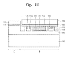
- FIG. 1B is a sectional view taken along line I-I' of FIG. 1A ;
- FIG. 1C is an enlarged plan view illustrating a portion A of FIG. 1A ;
- FIGS. 2A through 2F are sectional views taken along line I-I' of FIG. 1A , for explaining a method of fabricating the optical device according to an embodiment of the inventive concept;
- FIG. 3A is a plan view of an optical device according to another embodiment of the inventive concept.
- FIG. 3B is a sectional view taken along line II-II' of FIG. 3A ;
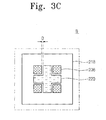
- FIG. 3C is an enlarged plan view illustrating a portion B of FIG. 3A ;
- FIGS. 4A through 4F are sectional views taken along line II-II' of FIG. 3A , for explaining a method of fabricating the optical device according to another embodiment of the inventive concept.
- an etching region illustrated in a right angle shape may have a rounded shape or a shape having a predetermined curvature.
- Areas exemplified in the drawings have general properties and are used to illustrate a specific shape of a semiconductor package region. Thus, this should not be construed as limited to the scope of the present invention.
- FIG. 1A is a plan view of an optical device according to an embodiment of the inventive concept
- FIG. 1B is a sectional view taken along line I-I' of FIG. 1A
- FIG. 1C is an enlarged plan view illustrating a portion A of FIG. 1A .
- an optical device may include a planar lightwave circuit (PLC) platform having a light waveguide region L and a mounting region M and an optical active chip 130 mounted on the mounting region M of the PLC platform.
- PLC planar lightwave circuit
- the PLC platform may include a substrate 110.
- the substrate 110 may include a silicon (Si) substrate.
- a PLC waveguide including a lower-clad layer 112, a PLC (platform) core 114, and an upper-clad layer 116 may be disposed on the light waveguide region L of the PLC platform.
- the lower-clad layer 112, the PLC core 114, and the upper-clad layer 116 may be formed of silica.
- the PLC waveguide may include a silica light waveguide.
- a terrace 118 having a trench 119 formed by etching the lower-clad layer 112 may be disposed on the mounting region M of the PLC platform.
- a platform under bump metallurgy (UBM) 122 may be disposed on the lower-clad layer 112 around the terrace 118 on the mounting region M of the PLC platform.
- the platform UBM 122 may include a 3-layer of Cr/Ni/Au, NiCr/Ni/Au, Ti/Ni/Au, Cr/Pt/Au, NiCr/Pt/Au, or Ti/Pt/Au or a 2-layer of Ni/Au.
- the optical active chip 130 may include a chip core 132 therein.
- the optical active chip 130 may include a laser diode or a photodiode.
- a chip UBM 134 and a chip alignment mark 136 may be disposed on a mounting surface of the optical active chip 130.
- the chip UBM 134 may include a 3-layer of Cr/Ni/Au, NiCr/Ni/Au, Ti/Ni/Au, Cr/Pt/Au, NiCr/Pt/Au, or Ti/Pt/Au or a 2-layer of Ni/Au.
- the chip alignment mark 136 may be formed of the same material as the chip UBM 134.
- the optical active chip 130 may be mounted on the mounting region M of the PLC platform using flip-chip (F/C) bonding. That is, the optical active chip 130 may be mounted on the mounting region M of the PLC platform to electrically connect the platform UBM 122 to the chip UBM 134 by a solder film 140.
- the solder film 140 may include an AuSn solder.
- the solder film 140 may have a thickness ranging from about 2 ⁇ m to about 8 ⁇ m.
- the chip core 132 of the optical active chip 130 such as the laser diode or the photodiode is disposed within a range of about 2 ⁇ m to about 5 ⁇ m from a mounting surface (p-side surface) of the optical active chip 130, it may not be necessary to deeply etch the mounting region M of the PLC platform.
- the solder film 140 having a thickness of several micrometers may be used.
- An inner circumference surface of the trench 119 of the terrace 118 may have a shape corresponding to that of an outer circumference surface of the chip alignment mark 136 of the optical active chip 130.
- a plane section of the chip alignment mark 136 of the optical active chip 130 is a closed figure
- a plane section of the inner circumference surface of the trench 119 of the terrace 118 may be a closed figure having the same configuration with an area greater than that of the plane section of the chip alignment mark 136 of the optical active chip 130.
- the plane section of the inner circumference surface of the trench 119 of the terrace 118 may be a closed figure having the same configuration with an area greater than that of the outer circumference surface of the chip alignment mark 136 contacting and surrounding the plurality of patterns.
- the optical active chip 130 may be aligned by interlocking between the trench 119 of the terrace 118 and the chip alignment mark 136 of the optical active chip 130 and mounted on the mounting region M of the PLC platform.
- the optical active chip 130 is not vertically moved by the terrace 118, and thus vertically aligned with the PLC platform.
- the optical active chip 130 is not horizontally moved by the interlocking between the trench 119 of the terrace 118 and the chip alignment mark 136 of the optical active chip 130, and thus horizontally aligned with the PLC platform.
- a commercialized F/C bonding equipment has alignment accuracy of about 1 ⁇ m.
- the optical active chip 130 and the PLC platform are aligned with each other using the commercialized F/C bonding equipment. Thereafter, when a predetermined load is applied to only contact the optical active chip 130 with the PLC platform, alignment accuracy therebetween is determined by the alignment accuracy of the F/C bonding equipment.
- the temperature of the F/C bonding equipment increases to melt the solder film 140 disposed between the optical active chip 130 and the PLC platform, significant misalignment may occur during the melting of the solder film 140 due to the difference of thermal expansion coefficients between the optical active chip 130, the PLC platform, and the F/C bonding equipment.
- the optical active chip 130 may be slipped by a molten solder in case where an excessively large amount of the molten solder is provided. As a result, the misalignment of more than several micrometers may occur, and thus, the optical coupling efficiency may be significantly reduced.
- the optical device according to an embodiment of the inventive concept is not horizontally moved by the interlocking between the trench 119 of the terrace 118 and the chip alignment mark 136 of the optical active chip 130, the misalignment occurring when the solder film 140 is melted to mount the optical active chip 130 on the PLC platform may be minimized.
- a distance D between the inner circumference surface of the trench 119 of the terrace 118 and the outer circumference surface of the chip alignment mark 136 of the optical active chip 130 may range from about 1 ⁇ m to about 2 ⁇ m.
- the alignment occurs when the solder film 140 is melted to mount the optical active chip 130 on the PLC platform, the alignment accuracy within about 2 ⁇ m may be secured.
- An additional solder film 140c may be further disposed on the chip alignment mark 136.
- the additional solder film 140c may additionally provide a vertical height difference for forming an interlocking structure between the trench 119 of the terrace 118 and the chip alignment mark 136 of the optical active chip 130.
- the additional solder film 140c may be melted when the optical active chip 130 is mounted on the PLC platform to further closely attach the optical active chip 130 to the trench 119 of the terrace 118. Therefore, the alignment accuracy may be further improved.
- a distance between the PLC waveguide and the optical active chip 130 may range from about 2.5 ⁇ m to about 20 ⁇ m.
- FIGS. 2A through 2F are sectional views taken along line I-I' of FIG. 1A , for explaining a method of fabricating the optical device according to an embodiment of the inventive concept.
- a lower-clad layer 112, a PLC core 114, and an upper-clad layer 116 may be sequentially formed on a substrate 110 including a light waveguide region L and a mounting region M.
- the substrate 110 may include a Si substrate.
- the lower-clad layer 112, the PLC core 114, and the upper-clad layer 116 may be formed of a silica film.
- a first etch process is performed on the upper-clad layer 116, the PLC core 114, and the lower-clad layer 112 disposed on the mounting region M of the substrate 110 to form a PLC waveguide including the lower-clad layer 112, the PCL core 114, and the upper-clad layer 116 in the light waveguide region L and the lower-clad layer 112 having a first height h1 in the mounting region M.
- the PLC waveguide may include a silica light waveguide.
- a second etch process is performed on the lower-clad layer 112 having the first height h1 in the mounting region M of the substrate 110 to form a terrace 118 having the first height h1 and a trench 119 and the lower-clad layer 112 having a second height h2.
- the trench 119 may be formed together with the terrace 118 having the first height h1 by simply changing a shape of a photomask pattern used for the second etch process for forming the terrace 118 having the first height h1. Thus, an additional process for forming the trench 119 is not required.
- a platform UBM 122 may be formed on the lower-clad layer 112 having the second height h2 around the terrace 118 formed on the mounting region M of the substrate 110.
- the platform UBM 122 may include a 3-layer of Cr/Ni/Au, NiCr/Ni/Au, Ti/Ni/Au, Cr/Pt/Au, NiCr/Pt/Au, or Ti/Pt/Au or a 2-layer of Ni/Au.
- the PLC waveguide may be formed in the light waveguide region L, and a PLC platform including the terrace 118 having the trench 119 may be formed in the mounting region M.
- a solder film 140a for platform is formed on the platform UBM 122.
- the solder film 140a for platform may include an AuSn solder.
- the solder film 140a for platform may have a thickness ranging from about 1 ⁇ m to about 4 ⁇ m.
- a solder film for chip see reference numeral 140b of FIG. 2E
- a sufficient thickness about 2 ⁇ m to 8 ⁇ m
- the formation of the solder film 140a for platform may be omitted.
- the optical active chip 130 including a chip core 132 therein is prepared.
- the optical active chip 130 may include a laser diode or a photodiode.
- the chip UBM 134 and a chip alignment mark 136 are formed on the mounting surface of the optical active chip 130.
- Each of the chip UBM 134 and the chip alignment mark 136 may include a 3-layer of Cr/Ni/Au, NiCr/Ni/Au, Ti/Ni/Au, Cr/Pt/Au, NiCr/Pt/Au, or Ti/Pt/Au or a 2-layer of Ni/Au.
- the chip UBM 134 and the chip alignment mark 136 may be formed using processes and materials different from each other or formed at the same time using the same process and material.
- An inner circumference surface of the trench 119 of the terrace 118 may have a shape corresponding to that of an outer circumference surface of the chip alignment mark 136 of the optical active chip 130.
- a plane section of the chip alignment mark 136 of the optical active chip 130 is a closed figure
- a plane section of the inner circumference surface of the trench 119 of the terrace 118 may be a closed figure having the same configuration with an area greater than that of the plane section of the chip alignment mark 136 of the optical active chip 130.
- the plane section of the inner circumference surface of the trench 119 of the terrace 118 may be a closed figure having the same configuration with an area greater than that of the outer circumference surface of the chip alignment mark 136 contacting and surrounding the plurality of patterns.
- a distance (see reference symbol D of FIG. 1C ) between the inner circumference surface of the trench 119 of the terrace 118 and the outer circumference surface of the chip alignment mark 136 may range from about 1 ⁇ m to about 2 ⁇ m.
- the solder film 140b for chip is formed on the chip UBM 134.
- the solder film 140b for chip may include an AuSn solder.
- the solder film 140b for chip may have a thickness ranging from about 1 ⁇ m to about 4 ⁇ m.
- the solder film 140a for platform having the sufficient thickness about 2 ⁇ m to 8 ⁇ m
- the formation of the solder film 140b for chip may be omitted.
- an additional solder film 140c may be further formed on the chip alignment nark 136.
- the additional solder film 140c may additionally provide a vertical height difference for forming an interlocking structure between the trench 119 of the terrace 118 and the chip alignment mark 136 of the optical active chip 130 when the optical active chip 130 is mounted on the mounting region M of the PLC platform (see FIG. 2F ).
- the additional solder film 140c may be melted when the optical active chip 130 is mounted on the PLC platform to further closely attach the optical active chip 130 to the trench 119 of the terrace 118. Therefore, the alignment accuracy may be further improved.
- the optical active chip 130 is mounted on the mounting region M of the substrate 110 to electrically connect the platform UBM 122 to the chip UBM 134 by a solder film 140.
- the solder film 140 may represents a solder film formed on the platform UBM 122 or the chip UBM 134 or all of the solder film 140a for platform and the solder film 140b for chip formed on the platform UBM 122 and the chip UBM 134, respectively.
- the optical active chip 130 may be aligned by interlocking between the trench 119 of the terrace 118 and the chip alignment mark 136 of the optical active chip 130 and mounted on the mounting region M of the PLC platform.
- the optical active chip 130 is not vertically moved by the terrace 118 and therefore vertically aligned with the PLC platform.
- the optical active chip 130 is not horizontally moved by the interlocking between the trench 119 of the terrace 118 and the chip alignment mark 136 of the optical active chip 130 and thus horizontally aligned with the PLC platform.
- a commercialized F/C bonding equipment has alignment accuracy of about 1 ⁇ m.
- the optical active chip 130 and the PLC platform are aligned with each other using the commercialized F/C bonding equipment. Thereafter, when a predetermined load is applied to only contact the optical active chip 130 with the PLC platform, alignment accuracy therebetween is determined by the alignment accuracy of the F/C bonding equipment.
- the temperature of the F/C bonding equipment increases to melt the solder film 140 disposed between the optical active chip 130 and the PLC platform, significant misalignment may occur during the melting of the solder film 140 due to the difference of thermal expansion coefficients between the optical active chip 130, the PLC platform, and the F/C bonding equipment.
- the optical active chip 130 may be slipped by a molten solder in case where an excessively large amount of the molten solder is provided. As a result, the misalignment of more than several micrometers may occur, and thus, the optical coupling efficiency may be significantly reduced.
- the optical device according to an embodiment of the inventive concept is not horizontally moved by the interlocking between the trench 119 of the terrace 118 and the chip alignment mark 136 of the optical active chip 130, the misalignment occurring when the solder film 140 is melted to mount the optical active chip 130 on the PLC platform may be minimized.
- a distance between the inner circumference surface of the trench 119 of the terrace 118 and the outer circumference surface of the chip alignment mark 136 of the optical active chip 130 may range from about 1 ⁇ m to about 2 ⁇ m.
- the alignment occurs when the solder film 140 is melted to mount the optical active chip 130 on the PLC platform, the alignment accuracy within about 2 ⁇ m may be secured.
- a distance between the PLC waveguide and the optical active chip 130 may range from about 2.5 ⁇ m to about 20 ⁇ m.
- FIG. 3A is a plan view of an optical device according to another embodiment of the inventive concept
- FIG. 3B is a sectional view taken along line II-II' of FIG. 3A
- FIG. 3C is an enlarged plan view illustrating a portion B of FIG. 3A .
- an optical device may include a PLC platform having a light waveguide region L and a mounting region M and an optical active chip 230 mounted on the mounting region M of the PLC platform.
- the PLC platform may include a substrate 210.
- the substrate 210 may include a Si substrate.
- a PLC waveguide including a lower-clad layer 212, a PLC core 214, and an upper-clad layer 216 may be disposed on the light waveguide region L of the PLC platform.
- the lower-clad layer 212, the PLC core 214, and the upper-clad layer 216 may be formed of silica.
- the PLC waveguide may include a silica light waveguide.
- a terrace 218 formed by etching the lower-clad layer 212 may be disposed on the mounting region M of the PLC platform.
- a platform UBM 222 may be disposed on the lower-clad layer 212 around the terrace 218 on the mounting region M of the PLC platform.
- the platform UBM 222 may include a 3-layer of Cr/Ni/Au, NiCr/Ni/Au, Ti/Ni/Au, Cr/Pt/Au, NiCr/Pt/Au, or Ti/Pt/Au or a 2-layer of Ni/Au.
- a platform alignment mark 220 may be disposed on an upper surface of the terrace 218.
- the platform alignment mark 220 may be formed of the same material as the platform UBM 222.
- the optical active chip 230 may include a chip core 232 therein.
- the optical active chip 230 may include a laser diode or a photodiode.
- a chip UBM 234 and a chip alignment mark 236 may be disposed on a mounting surface of the optical active chip 230.
- the chip UBM 234 may include a 3-layer of Cr/Ni/Au, NiCr/Ni/Au, Ti/Ni/Au, Cr/Pt/Au, NiCr/Pt/Au, or Ti/Pt/Au or a 2-layer of Ni/Au.
- the chip alignment mark 236 may be formed of the same material as the chip UBM 234.
- the optical active chip 230 may be mounted on the mounting region M of the PLC-platform using F/C bonding. That is, the optical active chip 230 may be mounted on the mounting region M of the PLC platform to electrically connect the platform UBM 222 to the chip UBM 234 by a solder film 240.
- the solder film 240 may include an AuSn solder.
- the solder film 240 may have a thickness ranging from about 2 ⁇ m to about 8 ⁇ m.
- the chip core 232 of the optical active chip 230 such as the laser diode and the photodiode is disposed within a range of about 2 ⁇ m to about 5 ⁇ m from a mounting surface (p-side surface) of the optical active chip 230, it may not be necessary to deeply etch the mounting region M of the PLC platform.
- the solder film 240 having a thickness of several micrometers may be used.
- the platform alignment mark 220 on the terrace 218 and the chip alignment mark 236 of the optical active chip 230 may have intaglio and relief shapes corresponding to each other, respectively.
- the platform alignment mark 220 on the terrace 218 may be a closed figure having the same configuration with an area less or greater than the closed figure of the chip alignment mark 236 of the optical active chip 230.
- the platform alignment mark 220 on the terrace 218 may be a closed figure or a plurality of patterns having a different configuration, which fills inner spaces between the plurality of patterns.
- the chip alignment mark 236 of the optical active chip 230 may be a closed figure or a plurality of patterns having a different configuration, which fills inner spaces between the plurality of patterns.
- the optical active chip 230 may be aligned by interlocking between the platform alignment mark 220 on the terrace 218 and the chip alignment mark 236 of the optical active chip 230 and mounted on the mounting region M of the PLC platform. Thus, the optical active chip 230 may not be vertically and horizontally moved by the interlocking between the platform alignment mark 220 on the terrace 218 and the chip alignment mark 236, and thus vertically and horizontally aligned with the PLC platform.
- a commercialized F/C bonding equipment has alignment accuracy of about 1 ⁇ m.
- the optical active chip 230 and the PLC platform are aligned with each other using the commercialized F/C bonding equipment. Thereafter, when a predetermined load is applied to only contact the optical active chip 230 with the PLC platform, alignment accuracy therebetween is determined by the alignment accuracy of the F/C bonding equipment.
- the optical active chip 230 may be mounted on the PLC platform, when the temperature of the F/C bonding equipment increases to melt the solder film 240 disposed between the optical active chip 230 and the PLC platform, significant misalignment may occur during the melting of the solder film 240 due to the difference of thermal expansion coefficients between the optical active chip 230, the PLC platform, and the F/C bonding equipment. Also, when the solder film 240 is melted, the optical active chip 230 may be slipped by a molten solder in case where an excessively large amount of the molten solder is provided. As a result, the misalignment of more than several micrometers may occur, and thus, the optical coupling efficiency may be significantly reduced.
- the optical device according to an embodiment of the inventive concept is not horizontally moved by the interlocking between the platform alignment mark 220 on the terrace 218 and the chip alignment mark 236 of the optical active chip 230, the misalignment occurring when the solder film 240 is melted to mount the optical active chip 230 on the PLC platform may be minimized.
- a distance D between the platform alignment mark 220 on the terrace 218 and the chip alignment mark 236 of the optical active chip 230 may range from about 1 ⁇ m to about 2 ⁇ m.
- the alignment occurs when the solder film 240 is melted to mount the optical active chip 230 on the PLC platform, the alignment accuracy within about 2 ⁇ m may be secured.
- a distance between the PLC waveguide and the optical active chip 230 may range from about 2.5 ⁇ m to about 20 ⁇ m.
- FIGS. 4A through 4F are sectional views taken along line II-II' of FIG. 3A , for explaining a method of fabricating the optical device according to another embodiment of the inventive concept.
- a lower-clad layer 212, a PLC core 214, and an upper-clad layer 216 may be sequentially formed on a substrate 210 including a light waveguide region L and a mounting region M.
- the substrate 210 may include a Si substrate.
- the lower-clad layer 212, the PLC core 214, and the upper-clad layer 216 may be formed of a silica film.
- a first etch process is performed on the upper-clad layer 216, the PLC core 214, and the lower-clad layer 212 disposed on the mounting region M of the substrate 210 to form a PLC waveguide including the lower-clad layer 212, the PCL core 214, and the upper-clad layer 216 in the light waveguide region L and the lower-clad layer 212 having a first height h1 in the mounting region M.
- the PLC waveguide may include a silica light waveguide.
- a second etch process is performed on the lower-clad layer 212 having the first height h1 in the mounting region M of the substrate 210 to form a terrace 218 having the first height h1 and the lower-clad layer 212 having a second height h2.
- a platform alignment mark 220 and a platform UBM 222 are formed on an upper surface of the terrace 218 and the lower-clad layer 212 having the second height h2 around the terrace 218 in the mounting region M of the substrate 210, respectively.
- Each of the platform alignment mark 220 and the platform UBM 222 may include a 3-layer of Cr/Ni/Au, NiCr/Ni/Au, Ti/Ni/Au, Cr/Pt/Au, NiCr/Pt/Au, or Ti/Pt/Au or a 2-layer of Ni/Au.
- the platform alignment mark 220 and the platform UBM 222 may be formed using processes and materials different from each other or formed at the same time using the same process and material.
- the platform alignment mark 220 may be formed together with the platform UBM 222 in deposition and patterning processes for forming the platform UBM 222. Thus, an additional process for forming the platform alignment mark 220 is not required.
- the PLC waveguide may be formed in the light waveguide region L, and a PLC platform including the terrace 218 having the platform alignment mark 220 may be formed in the mounting region M.
- a solder film 240a for platform is formed on the platform UBM 222.
- the solder film 240a for platform may include an AuSn solder.
- the solder film 240a for platform may have a thickness ranging from about 1 ⁇ m to about 4 ⁇ m.
- a solder film for chip see reference numeral 240b of FIG. 4E
- a sufficient thickness about 2 ⁇ m to 8 ⁇ m
- the formation of the solder film 240a for platform may be omitted.
- the optical active chip 230 including a chip core 232 therein is prepared.
- the optical active chip 230 may include a laser diode or a photodiode.
- the chip UBM 234 and a chip alignment mark 236 are formed on the mounting surface of the optical active chip 230.
- Each of the chip UBM 234 and the chip alignment mark 236 may include a 3-layer of Cr/Ni/Au, NiCr/Ni/Au, Ti/Ni/Au, Cr/Pt/Au, NiCr/Pt/Au, or Ti/Pt/Au or a 2-layer of Ni/Au.
- the chip UBM 234 and the chip alignment mark 236 may be formed using processes and materials different from each other or formed at the same time using the same process and material.
- the platform alignment mark 220 on the terrace 218 and the chip alignment mark 236 of the optical active chip 230 may have intaglio and relief shapes corresponding to each other, respectively.
- the platform alignment mark 220 on the terrace 218 may be a closed figure having the same configuration with an area less or greater than the closed figure of the chip alignment mark 236 of the optical active chip 230.
- the platform alignment mark 220 on the terrace 218 may be a closed figure or a plurality of patterns having a different configuration, which fills inner spaces between the plurality of patterns.
- the chip alignment mark 236 of the optical active chip 230 may be a closed figure or a plurality of patterns having a different configuration, which fills inner spaces between the plurality of patterns.
- a distance (see reference symbol D of FIG. 3C ) between the platform alignment mark 220 on the terrace 218 and the chip alignment mark 236 of the optical active chip 230 may range from about 1 ⁇ m to about 2 ⁇ m.
- the solder film 240b for chip is formed on the chip UBM 234.
- the solder film 240b for chip may include an AuSn solder.
- the solder film 240b for chip may have a thickness ranging from about 1 ⁇ m to about 4 ⁇ m.
- the solder film 240a for platform having the sufficient thickness about 2 ⁇ m to 8 ⁇ m
- the formation of the solder film 240b for chip may be omitted.
- the optical active chip 230 is mounted on the mounting region M of the substrate 210 to electrically connect the platform UBM 222 to the chip UBM 234 by a solder film 240.
- the solder film 240 may represents a solder film formed on the platform UBM 222 or the chip UBM 234 or all of the solder film 240a for platform and the solder film 240b for chip formed on the platform UBM 222 and the chip UBM 234, respectively.
- the optical active chip 230 may be aligned by interlocking between the platform alignment mark 220 on the terrace 218 and the chip alignment mark 236 of the optical active chip 230 and mounted on the mounting region M of the PLC platform. Thus, the optical active chip 230 may not be vertically and horizontally moved by the interlocking between the platform alignment mark 220 on the terrace 218 and the chip alignment mark 236, and thus vertically and horizontally aligned with the PLC platform.
- a commercialized F/C bonding equipment has alignment accuracy of about 1 ⁇ m.
- the optical active chip 230 and the PLC platform are aligned with each other using the commercialized F/C bonding equipment. Thereafter, when a predetermined load is applied to only contact the optical active chip 230 with the PLC platform, alignment accuracy therebetween is determined by the alignment accuracy of the F/C bonding equipment.
- the optical active chip 230 may be mounted on the PLC platform, when the temperature of the F/C bonding equipment increases to melt the solder film 240 disposed between the optical active chip 230 and the PLC platform, significant misalignment may occur during the melting of the solder film 240 due to the difference of thermal expansion coefficients between the optical active chip 230, the PLC platform, and the F/C bonding equipment. Also, when the solder film 240 is melted, the optical active chip 230 may be slipped by a molten solder in case where an excessively large amount of the molten solder is provided. As a result, the misalignment of more than several micrometers may occur, and thus, the optical coupling efficiency may be significantly reduced.
- the optical device according to an embodiment of the inventive concept is not horizontally moved by the interlocking between the platform alignment mark 220 on the terrace 218 and the chip alignment mark 236 of the optical active chip 230, the misalignment occurring when the solder film 240 is melted to mount the optical active chip 230 on the PLC platform may be minimized.
- a distance D between the platform alignment mark 220 on the terrace 218 and the chip alignment mark 236 of the optical active chip 230 may range from about 1 ⁇ m to about 2 ⁇ m.
- the alignment occurs when the solder film 240 is melted to mount the optical active chip 230 on the PLC platform, the alignment accuracy within about 2 ⁇ m may be secured.
- a distance between the PLC waveguide and the optical active chip 230 may range from about 2.5 ⁇ m to about 20 ⁇ m.
- the respective optical devices according to the embodiments of the inventive concept have a structure in which the PLC platform and the optical active chip are flip-bonded using the interlocking therebetween.
- the optical device according to the embodiments of the inventive concept uses the solder film of several micrometers.
- the optical device in which expensive costs of solder formation process may be reduced may be provided.
- the solder film is formed on the PLC platform and the optical active chip, respectively, each of the solder films may become thinner.
- the optical device in which the costs of solder formation process may be additionally reduced may be provided.
- the existing PLC platform formation process may be used as it is.
- the respective optical devices according to the embodiments of the inventive concept have a structure in which the PLC platform and the optical active chip are flip-bonded using the interlocking therebetween, the misalignment that may occur during the melting of the solder film may be limited within about 2 ⁇ m.
- the optical device in which the optical coupling efficiency between the PLC platform and the optical active chip may be improved, and simultaneously, yield due to the F/C bonding may be maximized may be provided.
- the costs of solder formation process that are a major obstacle to commercialize the optical module using the PLC hybrid integration technology may be reduced.
- the yield and the optical coupling efficiency due to the F/C bonding may be improved.
- the productivity when the optical transceiver and optical amplification module are mass produced, the productivity may be improved, and the optical module may be low in price.
Landscapes
- Physics & Mathematics (AREA)
- General Physics & Mathematics (AREA)
- Optics & Photonics (AREA)
- Engineering & Computer Science (AREA)
- Microelectronics & Electronic Packaging (AREA)
- Optical Couplings Of Light Guides (AREA)
- Optical Integrated Circuits (AREA)
- Manufacturing & Machinery (AREA)
Abstract
Description
- This patent application claims priority of Korean Patent Application No.
10-2009-0097184, filed on October 13, 2009 - The present disclosure herein relates to optical devices and methods of fabricating the same, and more particularly, to optical devices in which an optical active chip such as a laser diode and a photodiode and a planar lightwave circuit platform having an integrated light waveguide are hybrid-coupled and methods of fabricating the same.
- In an optical network for high-speedily and effectively transmitting a large amount of data, it is necessary that an optical active device performing light source, optical detection, and optical amplification functions and a light waveguide in which optical wavelength division and optical multiplexing are possible are integrated to realize an optical transceiver and optical amplification module at a low price.
- Such integration technologies are divided into a monolithic integration technology in which an optical active device and a light waveguide are realized and integrated using an optical semiconductor that is a single material and a planar lightwave circuit (PLC) hybrid integration technology in which an optical active device and a PLC platform are integrated using a flip-chip (F/C) bonding.
- In the monolithic integration technology, when each of optical devices is integrated on a single substrate, it may be difficult to realize an optical transceiver module at a low price due to limitations in optimization of the optical devices, reproducibility, and productivity. On the other hand, in the PLC hybrid integration technology, an optical active device having optimal performances may be hybrid-integrated with a PLC platform having a light waveguide function and a wavelength division multiplexing (WDM) filter function to improve productivity. Thus, the PLC hybrid integration technology is considered as a core technology that may realize the optical transceiver and optical amplification module at a low price.
- A PLC platform may be easily manufactured using existing light waveguide manufacturing technologies and platform post-processes such as an etching process and a metal deposition process. Thus, since optical coupling efficiency between a semiconductor chip that is an optical active device and the PLC platform including an integrated light waveguide affects performances of a hybrid integrated device, it is necessary to devise and establish a F/C bonding structure and method, which may improve alignment accuracy therebetween.
- Embodiments of the inventive concept provide an optical device that may improve alignment accuracy to enhance optical coupling efficiency when an optical active chip is bonded to a PLC platform.
- Embodiments of the inventive concept also provide a method of fabricating an optical device, which may improve alignment accuracy to enhance optical coupling efficiency when an optical active chip is bonded to a PLC platform.
- The object of the present invention is not limited to the aforesaid, but other objects not described herein will be clearly understood by those skilled in the art from descriptions below.
- Embodiments of the inventive concept provide optical devices which include things as in the following: a substrate having a waveguide region and a mounting region; a planar lightwave circuit (PLC) waveguide including a lower-clad layer and an upper-clad layer on the waveguide region of the substrate and a platform core between the lower-clad layer and the upper-clad layer; a terrace defined by etching the lower-clad layer on the mounting region of the substrate, the terrace including a trench; a platform under bump metallurgy (UBM) disposed on the etched surface of the lower-clad layer around the terrace disposed on the mounting region of the substrate; an optical active chip mounted on the mounting region of the substrate and including a chip core therein; a chip UBM and a chip alignment mark disposed on a mounting surface of the optical active chip; and a solder film electrically connecting the platform UBM to the chip UBM. The optical active chip is aligned by interlocking between the trench of the terrace and the chip alignment mark of the optical active chip and mounted on the mounting region.
- In some embodiments, a distance between an inner circumference surface of the trench of the terrace and an outer circumference surface of the chip alignment mark of the optical active chip may range from about 1 µm to about 2 µm.
- In other embodiments, the solder film may have a thickness ranging from about 2 µm to about 8 µm.
- In still other embodiments, the solder film may include an AuSn solder.
- In even other embodiments, the optical devices may further include an additional solder film disposed on the chip alignment mark.
- In yet other embodiments, a distance between the PLC waveguide and the optical active chip may range from about 2.5 µm to about 20 µm.
- In other embodiments of the inventive concept, other optical devices include things as follows: a substrate having a waveguide region and a mounting region; a PLC waveguide including a lower-clad layer and an upper-clad layer on the waveguide region of the substrate and a platform core between the lower-clad layer and the upper-clad layer; a terrace defined by etching the lower-clad layer on the mounting region of the substrate; a platform UBM disposed on the etched surface of the lower-clad layer around the terrace disposed on the mounting region of the substrate; a platform alignment mark disposed on an upper surface of the terrace; an optical active chip mounted on the mounting region of the substrate and including a chip core therein; a chip UBM and a chip alignment mark disposed on a mounting surface of the optical active chip; and a solder film electrically connecting the platform UBM to the chip UBM. The optical active chip is aligned by interlocking between the platform alignment mark of the terrace and the chip alignment mark of the optical active chip and mounted on the mounting region.
- In some embodiments, the platform alignment mark of the terrace and the chip alignment mark of the optical active chip may have intaglio and relief shapes corresponding to each other, respectively. A distance between the platform alignment mark of the terrace and the chip alignment mark of the optical active chip may range from about 1 µm to about 2 µm.
- In other embodiments, the solder film may have a thickness ranging from about 2 µm to about 8 µm.
- In still other embodiments, the solder film may include an AuSn solder.
- In even other embodiments, a distance between the PLC waveguide and the optical active chip may range from about 2.5 µm to about 20 µm.
- In still other embodiments of the inventive concept, methods of fabricating an optical device including: sequentially forming a lower-clad layer, a platform core, and an upper-clad layer on a substrate having a waveguide region and a mounting region; performing a first etch process on the upper-clad layer, the platform core, and the lower-clad layer disposed on the mounting region of the substrate to form a PLC waveguide in the waveguide region and a lower-clad layer having a first height in the mounting region; performing a second etch process on the lower-clad layer having the first height disposed on the mounting region of the substrate to form a terrace having the first height and a trench and a lower-clad layer having a second height; forming a platform UBM on the lower-clad layer having the second height around the terrace disposed on the mounting region of the substrate; forming a chip UBM on a mounting surface of the optical active chip including a chip core therein; forming a chip alignment mark on a mounting surface of an optical active chip; forming a solder film on at least one of the platform UBM and the chip UBM; and mounting the optical active chip on the mounting region of the substrate to electrically connect the platform UBM to the chip UBM by the solder film. The optical active chip is aligned by interlocking between the trench of the terrace and the chip alignment mark of the optical active chip and mounted on the mounting region.
- In some embodiments, a distance between an inner circumference surface of the trench of the terrace and an outer circumference surface of the chip alignment mark of the optical active chip may range from about 1 µm to about 2 µm.
- In other embodiments, the solder film may be formed on each of the platform UBM and the chip UBM. In this case, the solder film may have a thickness ranging from about 1 µm to about 4 µm.
- In still other embodiments, the solder film may include an AuSn solder.
- In even other embodiments, the chip UBM and the chip alignment mark may be formed at the same time.
- In yet other embodiments, the optical active chip may further include an additional solder film disposed on the chip alignment mark.
- In further embodiments, a distance between the PLC waveguide and the optical active chip may range from about 2.5 µm to about 20 µm.
- In even other embodiments of the inventive concept, methods of fabricating another optical device including: sequentially forming a lower-clad layer, a platform core, and an upper-clad layer on a substrate having a waveguide region and a mounting region; performing a first etch process on the upper-clad layer, the platform core, and the lower-clad layer disposed on the mounting region of the substrate to form a PLC waveguide in the waveguide region and a lower-clad layer having a first height in the mounting region; performing a second etch process on the lower-clad layer having the first height disposed on the mounting region of the substrate to form a terrace having the first height and a lower-clad layer having a second height; forming a platform UBM on the lower-clad layer having the second height around the terrace disposed on the mounting region of the substrate; forming a platform alignment mark on an upper surface of the terrace disposed on the mounting region of the substrate; forming a chip UBM on a mounting surface of the optical active chip including a chip core therein; forming a chip alignment mark on a mounting surface of an optical active chip; forming a solder film on at least one of the platform UBM and the chip UBM; and mounting the optical active chip on the mounting region of the substrate to electrically connect the platform UBM to the chip UBM by the solder film. The optical active chip is aligned by interlocking between the platform alignment mark of the terrace and the chip alignment mark of the optical active chip and mounted on the mounting region.
- In some embodiments, the platform alignment mark of the terrace and the chip alignment mark of the optical active chip may have intaglio and relief shapes corresponding to each other, respectively. A distance between the platform alignment mark of the terrace and the chip alignment mark of the optical active chip may range from about 1 µm to about 2 µm.
- In other embodiments, the solder film may be formed on each of the platform UBM and the chip UBM. The solder film may have a thickness ranging from about 1 µm to about 4 µm.
- In still other embodiments, the solder film may include an AuSn solder.
- In even other embodiments, the platform UBM and the platform alignment mark may be formed at the same time.
- In yet other embodiments, the chip UBM and the chip alignment mark may be formed at the same time.
- In further embodiments, a distance between the PLC waveguide and the optical active chip may range from about 2.5 µm to about 20 µm.
- The accompanying drawings are included to provide a further understanding of the inventive concept, and they are incorporated in and constitute a part of this specification. The drawings illustrate exemplary embodiments of the inventive concept and, together with the description, serve to explain principles of the inventive concept. In the figures:
-
FIG. 1A is a plan view of an optical device according to an embodiment of the inventive concept; -
FIG. 1B is a sectional view taken along line I-I' ofFIG. 1A ; -
FIG. 1C is an enlarged plan view illustrating a portion A ofFIG. 1A ; -
FIGS. 2A through 2F are sectional views taken along line I-I' ofFIG. 1A , for explaining a method of fabricating the optical device according to an embodiment of the inventive concept; -
FIG. 3A is a plan view of an optical device according to another embodiment of the inventive concept; -
FIG. 3B is a sectional view taken along line II-II' ofFIG. 3A ; -
FIG. 3C is an enlarged plan view illustrating a portion B ofFIG. 3A ; and -
FIGS. 4A through 4F are sectional views taken along line II-II' ofFIG. 3A , for explaining a method of fabricating the optical device according to another embodiment of the inventive concept. - Preferred embodiments of the inventive concept will be described below in more detail with reference to the accompanying drawings. Advantages and features of the inventive concept, and implementation methods thereof will be clarified through following embodiments described with reference to the accompanying drawings. The inventive concept may, however, be embodied in different forms and should not be construed as limited to the embodiments set forth herein. Rather, these embodiments are provided so that this disclosure will be thorough and complete and will fully convey the scope of the inventive concept to those skilled in the art. Further, the inventive concept is only defined by scopes of claims. Like reference numerals refer to like elements throughout.
- In the following description, the technical terms are used only for explain a specific exemplary embodiment while not limiting the present invention. The terms of a singular form may include plural forms unless referred to the contrary. The meaning of "include," "comprise," "including," or "comprising," specifies a property, a region, a fixed number, a step, a process, an element and/or a component but does not exclude other properties, regions, fixed numbers, steps, processes, elements and/or components. Also, since preferred embodiments are provided below, the order of the reference numerals given in the description is not limited thereto. It will be understood that when an element such as a layer, film, region, or substrate is referred to as being "on" another element, it can be directly on the other element or intervening elements may also be present.
- Additionally, the embodiment in the detailed description will be described with sectional views as ideal exemplary views of the present invention. In the figures, the dimensions of layers and regions are exaggerated for clarity of illustration. Accordingly, shapes of the exemplary views may be modified according to manufacturing techniques and/or allowable errors. Therefore, the embodiments of the present invention are not limited to the specific shape illustrated in the exemplary views but may include other shapes that may be created according to manufacturing processes. For example, an etching region illustrated in a right angle shape may have a rounded shape or a shape having a predetermined curvature. Areas exemplified in the drawings have general properties and are used to illustrate a specific shape of a semiconductor package region. Thus, this should not be construed as limited to the scope of the present invention.
-
FIG. 1A is a plan view of an optical device according to an embodiment of the inventive concept,FIG. 1B is a sectional view taken along line I-I' ofFIG. 1A , andFIG. 1C is an enlarged plan view illustrating a portion A ofFIG. 1A . - Referring to
FIGS. 1A through 1C , an optical device may include a planar lightwave circuit (PLC) platform having a light waveguide region L and a mounting region M and an opticalactive chip 130 mounted on the mounting region M of the PLC platform. - The PLC platform may include a
substrate 110. Thesubstrate 110 may include a silicon (Si) substrate. - A PLC waveguide including a lower-clad
layer 112, a PLC (platform)core 114, and an upper-cladlayer 116 may be disposed on the light waveguide region L of the PLC platform. The lower-cladlayer 112, thePLC core 114, and the upper-cladlayer 116 may be formed of silica. Thus, the PLC waveguide may include a silica light waveguide. - A
terrace 118 having atrench 119 formed by etching the lower-cladlayer 112 may be disposed on the mounting region M of the PLC platform. A platform under bump metallurgy (UBM) 122 may be disposed on the lower-cladlayer 112 around theterrace 118 on the mounting region M of the PLC platform. Theplatform UBM 122 may include a 3-layer of Cr/Ni/Au, NiCr/Ni/Au, Ti/Ni/Au, Cr/Pt/Au, NiCr/Pt/Au, or Ti/Pt/Au or a 2-layer of Ni/Au. - The optical
active chip 130 may include achip core 132 therein. The opticalactive chip 130 may include a laser diode or a photodiode. Achip UBM 134 and achip alignment mark 136 may be disposed on a mounting surface of the opticalactive chip 130. Thechip UBM 134 may include a 3-layer of Cr/Ni/Au, NiCr/Ni/Au, Ti/Ni/Au, Cr/Pt/Au, NiCr/Pt/Au, or Ti/Pt/Au or a 2-layer of Ni/Au. Thechip alignment mark 136 may be formed of the same material as thechip UBM 134. - The optical
active chip 130 may be mounted on the mounting region M of the PLC platform using flip-chip (F/C) bonding. That is, the opticalactive chip 130 may be mounted on the mounting region M of the PLC platform to electrically connect theplatform UBM 122 to thechip UBM 134 by asolder film 140. Thesolder film 140 may include an AuSn solder. Thesolder film 140 may have a thickness ranging from about 2 µm to about 8 µm. - Since the
chip core 132 of the opticalactive chip 130 such as the laser diode or the photodiode is disposed within a range of about 2 µm to about 5 µm from a mounting surface (p-side surface) of the opticalactive chip 130, it may not be necessary to deeply etch the mounting region M of the PLC platform. Thus, thesolder film 140 having a thickness of several micrometers may be used. - An inner circumference surface of the
trench 119 of theterrace 118 may have a shape corresponding to that of an outer circumference surface of thechip alignment mark 136 of the opticalactive chip 130. When a plane section of thechip alignment mark 136 of the opticalactive chip 130 is a closed figure, a plane section of the inner circumference surface of thetrench 119 of theterrace 118 may be a closed figure having the same configuration with an area greater than that of the plane section of thechip alignment mark 136 of the opticalactive chip 130. On the other hand, as shown inFIGS. 1A and1C , when thechip alignment mark 136 of the opticalactive chip 130 includes a plurality of patterns, the plane section of the inner circumference surface of thetrench 119 of theterrace 118 may be a closed figure having the same configuration with an area greater than that of the outer circumference surface of thechip alignment mark 136 contacting and surrounding the plurality of patterns. - The optical
active chip 130 may be aligned by interlocking between thetrench 119 of theterrace 118 and thechip alignment mark 136 of the opticalactive chip 130 and mounted on the mounting region M of the PLC platform. Thus, the opticalactive chip 130 is not vertically moved by theterrace 118, and thus vertically aligned with the PLC platform. Also, the opticalactive chip 130 is not horizontally moved by the interlocking between thetrench 119 of theterrace 118 and thechip alignment mark 136 of the opticalactive chip 130, and thus horizontally aligned with the PLC platform. - Generally, a commercialized F/C bonding equipment has alignment accuracy of about 1 µm. The optical
active chip 130 and the PLC platform are aligned with each other using the commercialized F/C bonding equipment. Thereafter, when a predetermined load is applied to only contact the opticalactive chip 130 with the PLC platform, alignment accuracy therebetween is determined by the alignment accuracy of the F/C bonding equipment. However, to mount the opticalactive chip 130 on the PLC platform, when the temperature of the F/C bonding equipment increases to melt thesolder film 140 disposed between the opticalactive chip 130 and the PLC platform, significant misalignment may occur during the melting of thesolder film 140 due to the difference of thermal expansion coefficients between the opticalactive chip 130, the PLC platform, and the F/C bonding equipment. Also, when thesolder film 140 is melted, the opticalactive chip 130 may be slipped by a molten solder in case where an excessively large amount of the molten solder is provided. As a result, the misalignment of more than several micrometers may occur, and thus, the optical coupling efficiency may be significantly reduced. - However, since the optical device according to an embodiment of the inventive concept is not horizontally moved by the interlocking between the
trench 119 of theterrace 118 and thechip alignment mark 136 of the opticalactive chip 130, the misalignment occurring when thesolder film 140 is melted to mount the opticalactive chip 130 on the PLC platform may be minimized. - A distance D between the inner circumference surface of the
trench 119 of theterrace 118 and the outer circumference surface of thechip alignment mark 136 of the opticalactive chip 130 may range from about 1 µm to about 2 µm. Thus, although the alignment occurs when thesolder film 140 is melted to mount the opticalactive chip 130 on the PLC platform, the alignment accuracy within about 2 µm may be secured. - An
additional solder film 140c may be further disposed on thechip alignment mark 136. Theadditional solder film 140c may additionally provide a vertical height difference for forming an interlocking structure between thetrench 119 of theterrace 118 and thechip alignment mark 136 of the opticalactive chip 130. Besides, theadditional solder film 140c may be melted when the opticalactive chip 130 is mounted on the PLC platform to further closely attach the opticalactive chip 130 to thetrench 119 of theterrace 118. Therefore, the alignment accuracy may be further improved. - A distance between the PLC waveguide and the optical
active chip 130 may range from about 2.5 µm to about 20 µm. -
FIGS. 2A through 2F are sectional views taken along line I-I' ofFIG. 1A , for explaining a method of fabricating the optical device according to an embodiment of the inventive concept. - Referring to
FIG. 2A , a lower-cladlayer 112, aPLC core 114, and an upper-cladlayer 116 may be sequentially formed on asubstrate 110 including a light waveguide region L and a mounting region M. - The
substrate 110 may include a Si substrate. The lower-cladlayer 112, thePLC core 114, and the upper-cladlayer 116 may be formed of a silica film. - Referring to
FIG. 2B , a first etch process is performed on the upper-cladlayer 116, thePLC core 114, and the lower-cladlayer 112 disposed on the mounting region M of thesubstrate 110 to form a PLC waveguide including the lower-cladlayer 112, thePCL core 114, and the upper-cladlayer 116 in the light waveguide region L and the lower-cladlayer 112 having a first height h1 in the mounting region M. Thus, the PLC waveguide may include a silica light waveguide. - Referring to
FIG. 2C , a second etch process is performed on the lower-cladlayer 112 having the first height h1 in the mounting region M of thesubstrate 110 to form aterrace 118 having the first height h1 and atrench 119 and the lower-cladlayer 112 having a second height h2. - The
trench 119 may be formed together with theterrace 118 having the first height h1 by simply changing a shape of a photomask pattern used for the second etch process for forming theterrace 118 having the first height h1. Thus, an additional process for forming thetrench 119 is not required. - Referring to
FIG. 2D , aplatform UBM 122 may be formed on the lower-cladlayer 112 having the second height h2 around theterrace 118 formed on the mounting region M of thesubstrate 110. Theplatform UBM 122 may include a 3-layer of Cr/Ni/Au, NiCr/Ni/Au, Ti/Ni/Au, Cr/Pt/Au, NiCr/Pt/Au, or Ti/Pt/Au or a 2-layer of Ni/Au. - Thus, the PLC waveguide may be formed in the light waveguide region L, and a PLC platform including the
terrace 118 having thetrench 119 may be formed in the mounting region M. - A
solder film 140a for platform is formed on theplatform UBM 122. Thesolder film 140a for platform may include an AuSn solder. Thesolder film 140a for platform may have a thickness ranging from about 1 µm to about 4 µm. When a solder film for chip (see reference numeral 140b ofFIG. 2E ) having a sufficient thickness (about 2 µm to 8 µm) is formed on a chip UBM (seereference numeral 134 ofFIG. 2E ) formed on a mounting surface of an optical active chip (seereference numeral 130 ofFIG. 2E ), the formation of thesolder film 140a for platform may be omitted. - Referring to
FIG. 2E , the opticalactive chip 130 including achip core 132 therein is prepared. The opticalactive chip 130 may include a laser diode or a photodiode. - The
chip UBM 134 and achip alignment mark 136 are formed on the mounting surface of the opticalactive chip 130. Each of thechip UBM 134 and thechip alignment mark 136 may include a 3-layer of Cr/Ni/Au, NiCr/Ni/Au, Ti/Ni/Au, Cr/Pt/Au, NiCr/Pt/Au, or Ti/Pt/Au or a 2-layer of Ni/Au. Thechip UBM 134 and thechip alignment mark 136 may be formed using processes and materials different from each other or formed at the same time using the same process and material. - An inner circumference surface of the
trench 119 of theterrace 118 may have a shape corresponding to that of an outer circumference surface of thechip alignment mark 136 of the opticalactive chip 130. When a plane section of thechip alignment mark 136 of the opticalactive chip 130 is a closed figure, a plane section of the inner circumference surface of thetrench 119 of theterrace 118 may be a closed figure having the same configuration with an area greater than that of the plane section of thechip alignment mark 136 of the opticalactive chip 130. On the other hand, as shown inFIGS. 1A and1C , when thechip alignment mark 136 of the opticalactive chip 130 includes a plurality of patterns, the plane section of the inner circumference surface of thetrench 119 of theterrace 118 may be a closed figure having the same configuration with an area greater than that of the outer circumference surface of thechip alignment mark 136 contacting and surrounding the plurality of patterns. A distance (see reference symbol D ofFIG. 1C ) between the inner circumference surface of thetrench 119 of theterrace 118 and the outer circumference surface of thechip alignment mark 136 may range from about 1 µm to about 2 µm. - The
solder film 140b for chip is formed on thechip UBM 134. Thesolder film 140b for chip may include an AuSn solder. Thesolder film 140b for chip may have a thickness ranging from about 1 µm to about 4 µm. When thesolder film 140a for platform having the sufficient thickness (about 2 µm to 8 µm) is formed on theplatform UBM 122 formed on the lower-cladlayer 112 having the second height h2 on the mounting region M of thesubstrate 110, the formation of thesolder film 140b for chip may be omitted. - When the
solder film 140b for chip is formed, anadditional solder film 140c may be further formed on thechip alignment nark 136. Theadditional solder film 140c may additionally provide a vertical height difference for forming an interlocking structure between thetrench 119 of theterrace 118 and thechip alignment mark 136 of the opticalactive chip 130 when the opticalactive chip 130 is mounted on the mounting region M of the PLC platform (seeFIG. 2F ). Besides, theadditional solder film 140c may be melted when the opticalactive chip 130 is mounted on the PLC platform to further closely attach the opticalactive chip 130 to thetrench 119 of theterrace 118. Therefore, the alignment accuracy may be further improved. - Referring to
FIG. 2F , the opticalactive chip 130 is mounted on the mounting region M of thesubstrate 110 to electrically connect theplatform UBM 122 to thechip UBM 134 by asolder film 140. - As described above, the
solder film 140 may represents a solder film formed on theplatform UBM 122 or thechip UBM 134 or all of thesolder film 140a for platform and thesolder film 140b for chip formed on theplatform UBM 122 and thechip UBM 134, respectively. - The optical
active chip 130 may be aligned by interlocking between thetrench 119 of theterrace 118 and thechip alignment mark 136 of the opticalactive chip 130 and mounted on the mounting region M of the PLC platform. Thus, the opticalactive chip 130 is not vertically moved by theterrace 118 and therefore vertically aligned with the PLC platform. Also, the opticalactive chip 130 is not horizontally moved by the interlocking between thetrench 119 of theterrace 118 and thechip alignment mark 136 of the opticalactive chip 130 and thus horizontally aligned with the PLC platform. - Generally, a commercialized F/C bonding equipment has alignment accuracy of about 1 µm. The optical
active chip 130 and the PLC platform are aligned with each other using the commercialized F/C bonding equipment. Thereafter, when a predetermined load is applied to only contact the opticalactive chip 130 with the PLC platform, alignment accuracy therebetween is determined by the alignment accuracy of the F/C bonding equipment. However, to mount the opticalactive chip 130 on the PLC platform, when the temperature of the F/C bonding equipment increases to melt thesolder film 140 disposed between the opticalactive chip 130 and the PLC platform, significant misalignment may occur during the melting of thesolder film 140 due to the difference of thermal expansion coefficients between the opticalactive chip 130, the PLC platform, and the F/C bonding equipment. Also, when thesolder film 140 is melted, the opticalactive chip 130 may be slipped by a molten solder in case where an excessively large amount of the molten solder is provided. As a result, the misalignment of more than several micrometers may occur, and thus, the optical coupling efficiency may be significantly reduced. - However, since the optical device according to an embodiment of the inventive concept is not horizontally moved by the interlocking between the
trench 119 of theterrace 118 and thechip alignment mark 136 of the opticalactive chip 130, the misalignment occurring when thesolder film 140 is melted to mount the opticalactive chip 130 on the PLC platform may be minimized. - A distance between the inner circumference surface of the
trench 119 of theterrace 118 and the outer circumference surface of thechip alignment mark 136 of the opticalactive chip 130 may range from about 1 µm to about 2 µm. Thus, although the alignment occurs when thesolder film 140 is melted to mount the opticalactive chip 130 on the PLC platform, the alignment accuracy within about 2 µm may be secured. - In the optical device fabricated using the above-described methods, a distance between the PLC waveguide and the optical
active chip 130 may range from about 2.5 µm to about 20 µm. -
FIG. 3A is a plan view of an optical device according to another embodiment of the inventive concept,FIG. 3B is a sectional view taken along line II-II' ofFIG. 3A , andFIG. 3C is an enlarged plan view illustrating a portion B ofFIG. 3A . - Referring to
FIGS. 3A through 3C , an optical device may include a PLC platform having a light waveguide region L and a mounting region M and an opticalactive chip 230 mounted on the mounting region M of the PLC platform. - The PLC platform may include a
substrate 210. Thesubstrate 210 may include a Si substrate. - A PLC waveguide including a lower-clad
layer 212, aPLC core 214, and an upper-cladlayer 216 may be disposed on the light waveguide region L of the PLC platform. The lower-cladlayer 212, thePLC core 214, and the upper-cladlayer 216 may be formed of silica. Thus, the PLC waveguide may include a silica light waveguide. - A
terrace 218 formed by etching the lower-cladlayer 212 may be disposed on the mounting region M of the PLC platform. Aplatform UBM 222 may be disposed on the lower-cladlayer 212 around theterrace 218 on the mounting region M of the PLC platform. Theplatform UBM 222 may include a 3-layer of Cr/Ni/Au, NiCr/Ni/Au, Ti/Ni/Au, Cr/Pt/Au, NiCr/Pt/Au, or Ti/Pt/Au or a 2-layer of Ni/Au. Aplatform alignment mark 220 may be disposed on an upper surface of theterrace 218. Theplatform alignment mark 220 may be formed of the same material as theplatform UBM 222. - The optical
active chip 230 may include achip core 232 therein. The opticalactive chip 230 may include a laser diode or a photodiode. Achip UBM 234 and achip alignment mark 236 may be disposed on a mounting surface of the opticalactive chip 230. Thechip UBM 234 may include a 3-layer of Cr/Ni/Au, NiCr/Ni/Au, Ti/Ni/Au, Cr/Pt/Au, NiCr/Pt/Au, or Ti/Pt/Au or a 2-layer of Ni/Au. Thechip alignment mark 236 may be formed of the same material as thechip UBM 234. - The optical
active chip 230 may be mounted on the mounting region M of the PLC-platform using F/C bonding. That is, the opticalactive chip 230 may be mounted on the mounting region M of the PLC platform to electrically connect theplatform UBM 222 to thechip UBM 234 by asolder film 240. Thesolder film 240 may include an AuSn solder. Thesolder film 240 may have a thickness ranging from about 2 µm to about 8 µm. - Since the
chip core 232 of the opticalactive chip 230 such as the laser diode and the photodiode is disposed within a range of about 2 µm to about 5 µm from a mounting surface (p-side surface) of the opticalactive chip 230, it may not be necessary to deeply etch the mounting region M of the PLC platform. Thus, thesolder film 240 having a thickness of several micrometers may be used. - The
platform alignment mark 220 on theterrace 218 and thechip alignment mark 236 of the opticalactive chip 230 may have intaglio and relief shapes corresponding to each other, respectively. When thechip alignment mark 236 of the opticalactive chip 230 is a closed figure having a dam shape, theplatform alignment mark 220 on theterrace 218 may be a closed figure having the same configuration with an area less or greater than the closed figure of thechip alignment mark 236 of the opticalactive chip 230. On the other hand, as shown inFIGS. 3A and3C , when thechip alignment mark 236 of the opticalactive chip 230 includes a plurality of patterns, theplatform alignment mark 220 on theterrace 218 may be a closed figure or a plurality of patterns having a different configuration, which fills inner spaces between the plurality of patterns. Also, when theplatform alignment mark 220 on theterrace 218 includes a plurality of patterns, thechip alignment mark 236 of the opticalactive chip 230 may be a closed figure or a plurality of patterns having a different configuration, which fills inner spaces between the plurality of patterns. - The optical
active chip 230 may be aligned by interlocking between theplatform alignment mark 220 on theterrace 218 and thechip alignment mark 236 of the opticalactive chip 230 and mounted on the mounting region M of the PLC platform. Thus, the opticalactive chip 230 may not be vertically and horizontally moved by the interlocking between theplatform alignment mark 220 on theterrace 218 and thechip alignment mark 236, and thus vertically and horizontally aligned with the PLC platform. - Generally, a commercialized F/C bonding equipment has alignment accuracy of about 1 µm. The optical
active chip 230 and the PLC platform are aligned with each other using the commercialized F/C bonding equipment. Thereafter, when a predetermined load is applied to only contact the opticalactive chip 230 with the PLC platform, alignment accuracy therebetween is determined by the alignment accuracy of the F/C bonding equipment. However, to mount the opticalactive chip 230 on the PLC platform, when the temperature of the F/C bonding equipment increases to melt thesolder film 240 disposed between the opticalactive chip 230 and the PLC platform, significant misalignment may occur during the melting of thesolder film 240 due to the difference of thermal expansion coefficients between the opticalactive chip 230, the PLC platform, and the F/C bonding equipment. Also, when thesolder film 240 is melted, the opticalactive chip 230 may be slipped by a molten solder in case where an excessively large amount of the molten solder is provided. As a result, the misalignment of more than several micrometers may occur, and thus, the optical coupling efficiency may be significantly reduced. - However, since the optical device according to an embodiment of the inventive concept is not horizontally moved by the interlocking between the
platform alignment mark 220 on theterrace 218 and thechip alignment mark 236 of the opticalactive chip 230, the misalignment occurring when thesolder film 240 is melted to mount the opticalactive chip 230 on the PLC platform may be minimized. - A distance D between the
platform alignment mark 220 on theterrace 218 and thechip alignment mark 236 of the opticalactive chip 230 may range from about 1 µm to about 2 µm. Thus, although the alignment occurs when thesolder film 240 is melted to mount the opticalactive chip 230 on the PLC platform, the alignment accuracy within about 2 µm may be secured. - A distance between the PLC waveguide and the optical
active chip 230 may range from about 2.5 µm to about 20 µm. -
FIGS. 4A through 4F are sectional views taken along line II-II' ofFIG. 3A , for explaining a method of fabricating the optical device according to another embodiment of the inventive concept. - Referring to
FIG. 4A , a lower-cladlayer 212, aPLC core 214, and an upper-cladlayer 216 may be sequentially formed on asubstrate 210 including a light waveguide region L and a mounting region M. - The
substrate 210 may include a Si substrate. The lower-cladlayer 212, thePLC core 214, and the upper-cladlayer 216 may be formed of a silica film. - Referring to
FIG. 4B , a first etch process is performed on the upper-cladlayer 216, thePLC core 214, and the lower-cladlayer 212 disposed on the mounting region M of thesubstrate 210 to form a PLC waveguide including the lower-cladlayer 212, thePCL core 214, and the upper-cladlayer 216 in the light waveguide region L and the lower-cladlayer 212 having a first height h1 in the mounting region M. Thus, the PLC waveguide may include a silica light waveguide. - Referring to
FIG. 4C , a second etch process is performed on the lower-cladlayer 212 having the first height h1 in the mounting region M of thesubstrate 210 to form aterrace 218 having the first height h1 and the lower-cladlayer 212 having a second height h2. - Referring to
FIG. 4D , aplatform alignment mark 220 and aplatform UBM 222 are formed on an upper surface of theterrace 218 and the lower-cladlayer 212 having the second height h2 around theterrace 218 in the mounting region M of thesubstrate 210, respectively. - Each of the
platform alignment mark 220 and theplatform UBM 222 may include a 3-layer of Cr/Ni/Au, NiCr/Ni/Au, Ti/Ni/Au, Cr/Pt/Au, NiCr/Pt/Au, or Ti/Pt/Au or a 2-layer of Ni/Au. Theplatform alignment mark 220 and theplatform UBM 222 may be formed using processes and materials different from each other or formed at the same time using the same process and material. - The
platform alignment mark 220 may be formed together with theplatform UBM 222 in deposition and patterning processes for forming theplatform UBM 222. Thus, an additional process for forming theplatform alignment mark 220 is not required. - Thus, the PLC waveguide may be formed in the light waveguide region L, and a PLC platform including the
terrace 218 having theplatform alignment mark 220 may be formed in the mounting region M. - A
solder film 240a for platform is formed on theplatform UBM 222. Thesolder film 240a for platform may include an AuSn solder. Thesolder film 240a for platform may have a thickness ranging from about 1 µm to about 4 µm. When a solder film for chip (see reference numeral 240b ofFIG. 4E ) having a sufficient thickness (about 2 µm to 8 µm) is formed on a chip UBM (seereference numeral 234 ofFIG. 4E ) formed on a mounting surface of an optical active chip (seereference numeral 230 ofFIG. 4E ), the formation of thesolder film 240a for platform may be omitted. - Referring to
FIG. 4E , the opticalactive chip 230 including achip core 232 therein is prepared. The opticalactive chip 230 may include a laser diode or a photodiode. - The
chip UBM 234 and achip alignment mark 236 are formed on the mounting surface of the opticalactive chip 230. Each of thechip UBM 234 and thechip alignment mark 236 may include a 3-layer of Cr/Ni/Au, NiCr/Ni/Au, Ti/Ni/Au, Cr/Pt/Au, NiCr/Pt/Au, or Ti/Pt/Au or a 2-layer of Ni/Au. Thechip UBM 234 and thechip alignment mark 236 may be formed using processes and materials different from each other or formed at the same time using the same process and material. - The
platform alignment mark 220 on theterrace 218 and thechip alignment mark 236 of the opticalactive chip 230 may have intaglio and relief shapes corresponding to each other, respectively. When thechip alignment mark 236 of the opticalactive chip 230 is a closed figure having a dam shape, theplatform alignment mark 220 on theterrace 218 may be a closed figure having the same configuration with an area less or greater than the closed figure of thechip alignment mark 236 of the opticalactive chip 230. On the other hand, as shown inFIGS. 4A and4C , when thechip alignment mark 236 of the opticalactive chip 230 includes a plurality of patterns, theplatform alignment mark 220 on theterrace 218 may be a closed figure or a plurality of patterns having a different configuration, which fills inner spaces between the plurality of patterns. Also, when theplatform alignment mark 220 on theterrace 218 includes a plurality of patterns, thechip alignment mark 236 of the opticalactive chip 230 may be a closed figure or a plurality of patterns having a different configuration, which fills inner spaces between the plurality of patterns. A distance (see reference symbol D ofFIG. 3C ) between theplatform alignment mark 220 on theterrace 218 and thechip alignment mark 236 of the opticalactive chip 230 may range from about 1 µm to about 2 µm. - The
solder film 240b for chip is formed on thechip UBM 234. Thesolder film 240b for chip may include an AuSn solder. Thesolder film 240b for chip may have a thickness ranging from about 1 µm to about 4 µm. When thesolder film 240a for platform having the sufficient thickness (about 2 µm to 8 µm) is formed on theplatform UBM 222 formed on the lower-cladlayer 212 having the second height h2 on the mounting region M of thesubstrate 210, the formation of thesolder film 240b for chip may be omitted. - Referring to
FIG. 4F , the opticalactive chip 230 is mounted on the mounting region M of thesubstrate 210 to electrically connect theplatform UBM 222 to thechip UBM 234 by asolder film 240. - As described above, the
solder film 240 may represents a solder film formed on theplatform UBM 222 or thechip UBM 234 or all of thesolder film 240a for platform and thesolder film 240b for chip formed on theplatform UBM 222 and thechip UBM 234, respectively. - The optical
active chip 230 may be aligned by interlocking between theplatform alignment mark 220 on theterrace 218 and thechip alignment mark 236 of the opticalactive chip 230 and mounted on the mounting region M of the PLC platform. Thus, the opticalactive chip 230 may not be vertically and horizontally moved by the interlocking between theplatform alignment mark 220 on theterrace 218 and thechip alignment mark 236, and thus vertically and horizontally aligned with the PLC platform. - Generally, a commercialized F/C bonding equipment has alignment accuracy of about 1 µm. The optical
active chip 230 and the PLC platform are aligned with each other using the commercialized F/C bonding equipment. Thereafter, when a predetermined load is applied to only contact the opticalactive chip 230 with the PLC platform, alignment accuracy therebetween is determined by the alignment accuracy of the F/C bonding equipment. However, to mount the opticalactive chip 230 on the PLC platform, when the temperature of the F/C bonding equipment increases to melt thesolder film 240 disposed between the opticalactive chip 230 and the PLC platform, significant misalignment may occur during the melting of thesolder film 240 due to the difference of thermal expansion coefficients between the opticalactive chip 230, the PLC platform, and the F/C bonding equipment. Also, when thesolder film 240 is melted, the opticalactive chip 230 may be slipped by a molten solder in case where an excessively large amount of the molten solder is provided. As a result, the misalignment of more than several micrometers may occur, and thus, the optical coupling efficiency may be significantly reduced. - However, since the optical device according to an embodiment of the inventive concept is not horizontally moved by the interlocking between the
platform alignment mark 220 on theterrace 218 and thechip alignment mark 236 of the opticalactive chip 230, the misalignment occurring when thesolder film 240 is melted to mount the opticalactive chip 230 on the PLC platform may be minimized. - A distance D between the
platform alignment mark 220 on theterrace 218 and thechip alignment mark 236 of the opticalactive chip 230 may range from about 1 µm to about 2 µm. Thus, although the alignment occurs when thesolder film 240 is melted to mount the opticalactive chip 230 on the PLC platform, the alignment accuracy within about 2 µm may be secured. - A distance between the PLC waveguide and the optical
active chip 230 may range from about 2.5 µm to about 20 µm. - The respective optical devices according to the embodiments of the inventive concept have a structure in which the PLC platform and the optical active chip are flip-bonded using the interlocking therebetween. Thus, unlike a typical optical device that uses a solder bump of more than several tens micrometers in order to use self-alignment of a solder, the optical device according to the embodiments of the inventive concept uses the solder film of several micrometers. Thus, the optical device in which expensive costs of solder formation process may be reduced may be provided. Also, since the solder film is formed on the PLC platform and the optical active chip, respectively, each of the solder films may become thinner. Thus, the optical device in which the costs of solder formation process may be additionally reduced may be provided.
- Also, in the methods of fabricating the optical device according to the embodiments of the inventive concept, since an additional process for forming a structure for the interlocking between the PLC platform and the optical active chip is not required, the existing PLC platform formation process may be used as it is. Thus, the optical device in which the structure for the interlocking between the PLC platform and the optical active chip may be easily realized, and simultaneously, additional process costs may not be required may be provided.
- In addition, since the respective optical devices according to the embodiments of the inventive concept have a structure in which the PLC platform and the optical active chip are flip-bonded using the interlocking therebetween, the misalignment that may occur during the melting of the solder film may be limited within about 2 µm. Thus, the optical device in which the optical coupling efficiency between the PLC platform and the optical active chip may be improved, and simultaneously, yield due to the F/C bonding may be maximized may be provided.
- Therefore, in the optical devices according to the embodiments of the inventive concept, the costs of solder formation process that are a major obstacle to commercialize the optical module using the PLC hybrid integration technology may be reduced. In addition, the yield and the optical coupling efficiency due to the F/C bonding may be improved. Also, in the optical devices according to the embodiments of the inventive concept, when the optical transceiver and optical amplification module are mass produced, the productivity may be improved, and the optical module may be low in price.
- The above-disclosed subject matter is to be considered illustrative and not restrictive, and the appended claims are intended to cover all such modifications, enhancements, and other embodiments, which fall within the true spirit and scope of the inventive concept. Thus, to the maximum extent allowed by law, the scope of the inventive concept is to be determined by the broadest permissible interpretation of the following claims and their equivalents, and it shall not be restricted or limited by the foregoing detailed description.
Claims (15)
- An optical device comprising:a substrate having a waveguide region and a mounting region;a planar lightwave circuit (PLC) waveguide comprising a lower-clad layer and an upper-clad layer on the waveguide region of the substrate and a platform core between the lower-clad layer and the upper-clad layer;a terrace defined by etching the lower-clad layer on the mounting region of the substrate, the terrace comprising an interlocking part;an optical active chip mounted on the mounting region of the substrate, the optical active chip comprising a chip core therein; anda chip alignment mark disposed on a mounting surface of the optical active chip,wherein the optical active chip is aligned by interlocking between the interlocking part of the terrace and the chip alignment mark of the optical active chip and mounted on the mounting region.
- The optical device of claim 1, wherein the interlocking part comprises a trench defined by etching the terrace and within the terrace.
- The optical device of claim 1 or 2, wherein the interlocking part comprises a platform alignment mark disposed on an upper surface of the terrace.
- The optical device of claim 3, wherein the platform alignment mark on the terrace and the chip alignment mark of the optical active chip have intaglio and relief shapes corresponding to each other, respectively.
- The optical device of any of the preceding claims, further comprising:a platform under bump metallurgy (UBM) disposed on the etched surface of the lower-clad layer around the terrace disposed on the mounting region of the substrate; anda chip UBM disposed on the mounting surface of the optical active chip.
- The optical device of claim 5, further comprising a solder film electrically connecting the platform UBM to the chip UBM.
- The optical device of any of the preceding claims, further comprising an additional solder film disposed on the chip alignment mark.
- A method of fabricating an optical device, the method comprising:sequentially forming a lower-clad layer, a platform core, and an upper-clad layer on a substrate having a waveguide region and a mounting region;performing a first etch process on the upper-clad layer, the platform core, and the lower-clad layer disposed on the mounting region of the substrate to form a PLC waveguide in the waveguide region and a lower-clad layer having a first height in the mounting region;performing a second etch process on the lower-clad layer having the first height disposed on the mounting region of the substrate to form a terrace having the first height and a trench and a lower-clad layer having a second height;forming a chip alignment mark on a mounting surface of an optical active chip comprising a chip core therein; andmounting the optical active chip on the mounting region of the substrate,wherein the optical active chip is aligned by interlocking between the trench of the terrace and the chip alignment mark of the optical active chip and mounted on the mounting region.
- The method of claim 8, further comprising:forming a platform UBM on the lower-clad layer having the second height around the terrace disposed on the mounting region of the substrate; andforming a chip UBM on the mounting surface of the optical active chip.
- The method of claim 9, further comprising forming a solder film on at least one of the platform UBM and the chip UBM.
- The method of any of claims 8 to 10, further comprising forming an additional solder film on the chip alignment mark.
- A method of fabricating an optical device, the method comprising:sequentially forming a lower-clad layer, a platform core, and an upper-clad layer on a substrate having a waveguide region and a mounting region;performing a first etch process on the upper-clad layer, the platform core, and the lower-clad layer disposed on the mounting region of the substrate to form a PLC waveguide in the waveguide region and a lower-clad layer having a first height in the mounting region;performing a second etch process on the lower-clad layer having the first height disposed on the mounting region of the substrate to form a terrace having the first height and a lower-clad layer having a second height;forming a platform alignment mark on an upper surface of the terrace disposed on the mounting region of the substrate;forming a chip alignment mark on a mounting surface of an optical active chip comprising a chip core therein; andmounting the optical active chip on the mounting region of the substrate,wherein the optical active chip is aligned by interlocking between the platform alignment mark on the terrace and the chip alignment mark of the optical active chip and mounted on the mounting region.
- The method of claim 12, wherein the platform alignment mark on the terrace and the chip alignment mark of the optical active chip have intaglio and relief shapes corresponding to each other, respectively.
- The method of claim 12 or 13, further comprising:forming a platform UBM on the lower-clad layer having the second height around the terrace disposed on the mounting region of the substrate; andforming a chip UBM on the mounting surface of the optical active chip.
- The method of claim 14, further comprising forming a solder film on at least one of the platform UBM and the chip UBM.
Applications Claiming Priority (1)
| Application Number | Priority Date | Filing Date | Title |
|---|---|---|---|
| KR1020090097184A KR101199302B1 (en) | 2009-10-13 | 2009-10-13 | Optical Device and Method of Fabricating the Same |
Publications (3)
| Publication Number | Publication Date |
|---|---|
| EP2312357A2 true EP2312357A2 (en) | 2011-04-20 |
| EP2312357A3 EP2312357A3 (en) | 2014-04-09 |
| EP2312357B1 EP2312357B1 (en) | 2017-11-08 |
Family
ID=42318135
Family Applications (1)
| Application Number | Title | Priority Date | Filing Date |
|---|---|---|---|
| EP10152992.3A Not-in-force EP2312357B1 (en) | 2009-10-13 | 2010-02-09 | Optical devices and methods of fabricating the same |
Country Status (3)
| Country | Link |
|---|---|
| US (2) | US8805129B2 (en) |
| EP (1) | EP2312357B1 (en) |
| KR (1) | KR101199302B1 (en) |
Cited By (3)
| Publication number | Priority date | Publication date | Assignee | Title |
|---|---|---|---|---|
| EP3382433A1 (en) * | 2017-03-28 | 2018-10-03 | Nokia Solutions and Networks Oy | Full wafer integration of iii-v devices |
| WO2021247994A1 (en) * | 2020-06-05 | 2021-12-09 | Siphox, Inc. | Systems and methods for photonic chip coupling |
| GB2613264A (en) * | 2018-11-02 | 2023-05-31 | Marvell Asia Pte Ltd | Silicon photonics based tunable laser |
Families Citing this family (53)
| Publication number | Priority date | Publication date | Assignee | Title |
|---|---|---|---|---|
| US9882073B2 (en) * | 2013-10-09 | 2018-01-30 | Skorpios Technologies, Inc. | Structures for bonding a direct-bandgap chip to a silicon photonic device |
| US9316785B2 (en) | 2013-10-09 | 2016-04-19 | Skorpios Technologies, Inc. | Integration of an unprocessed, direct-bandgap chip into a silicon photonic device |
| US8630326B2 (en) | 2009-10-13 | 2014-01-14 | Skorpios Technologies, Inc. | Method and system of heterogeneous substrate bonding for photonic integration |
| US11181688B2 (en) * | 2009-10-13 | 2021-11-23 | Skorpios Technologies, Inc. | Integration of an unprocessed, direct-bandgap chip into a silicon photonic device |
| US9922967B2 (en) | 2010-12-08 | 2018-03-20 | Skorpios Technologies, Inc. | Multilevel template assisted wafer bonding |
| US8518748B1 (en) * | 2011-06-29 | 2013-08-27 | Western Digital (Fremont), Llc | Method and system for providing a laser submount for an energy assisted magnetic recording head |
| US9977188B2 (en) | 2011-08-30 | 2018-05-22 | Skorpios Technologies, Inc. | Integrated photonics mode expander |
| US9097846B2 (en) | 2011-08-30 | 2015-08-04 | Skorpios Technologies, Inc. | Integrated waveguide coupler |
| CN103376514A (en) * | 2012-04-20 | 2013-10-30 | 鸿富锦精密工业(深圳)有限公司 | Optical fiber connector |
| US9217836B2 (en) * | 2012-10-23 | 2015-12-22 | Kotura, Inc. | Edge coupling of optical devices |
| JP6157911B2 (en) * | 2013-04-17 | 2017-07-05 | 富士通株式会社 | Optical semiconductor device |
| WO2014176561A1 (en) * | 2013-04-25 | 2014-10-30 | Skorpios Technologies, Inc. | Method and system for height registration during chip bonding |
| US9664855B2 (en) | 2014-03-07 | 2017-05-30 | Skorpios Technologies, Inc. | Wide shoulder, high order mode filter for thick-silicon waveguides |
| US10003173B2 (en) | 2014-04-23 | 2018-06-19 | Skorpios Technologies, Inc. | Widely tunable laser control |
| EP3149522A4 (en) | 2014-05-27 | 2018-02-21 | Skorpios Technologies, Inc. | Waveguide mode expander using amorphous silicon |
| US10319693B2 (en) | 2014-06-16 | 2019-06-11 | Skorpios Technologies, Inc. | Micro-pillar assisted semiconductor bonding |
| US9209142B1 (en) | 2014-09-05 | 2015-12-08 | Skorpios Technologies, Inc. | Semiconductor bonding with compliant resin and utilizing hydrogen implantation for transfer-wafer removal |
| US9606308B2 (en) * | 2015-02-27 | 2017-03-28 | International Business Machines Corporation | Three dimensional self-alignment of flip chip assembly using solder surface tension during solder reflow |
| US20160291269A1 (en) | 2015-04-01 | 2016-10-06 | Coriant Advanced Technology, LLC | Photonic integrated circuit chip packaging |
| EP3286587A4 (en) | 2015-04-20 | 2018-12-26 | Skorpios Technologies, Inc. | Vertical output couplers for photonic devices |
| US10168497B2 (en) * | 2015-06-15 | 2019-01-01 | Rwth Aachen | Self-alignment for apparatus comprising photonic device |
| TWI566918B (en) * | 2015-07-29 | 2017-01-21 | 財團法人工業技術研究院 | Three-dimensional printing system |
| US10234626B2 (en) * | 2016-02-08 | 2019-03-19 | Skorpios Technologies, Inc. | Stepped optical bridge for connecting semiconductor waveguides |
| CN105759373B (en) * | 2016-05-17 | 2018-02-02 | 武汉电信器件有限公司 | A kind of multicore Planar Optical Waveguide Structures and its coupled structure |
| CN105759343B (en) * | 2016-05-17 | 2018-03-02 | 武汉电信器件有限公司 | A kind of structure and its coupled structure and coupling process for mixing multicore planar optical waveguide |
| CN105759374B (en) * | 2016-05-17 | 2018-03-02 | 武汉电信器件有限公司 | A kind of Planar Optical Waveguide Structures and its coupled structure and coupling process |
| WO2017197881A1 (en) | 2016-05-17 | 2017-11-23 | 武汉电信器件有限公司 | Planar optical-waveguide structure, and coupling structure and coupling method thereof |
| US10295740B2 (en) * | 2016-07-07 | 2019-05-21 | Mellanox Technologies, Ltd. | Integrating silicon photonics and laser dies using flip-chip technology |
| JP6792384B2 (en) * | 2016-09-08 | 2020-11-25 | 富士通株式会社 | Optical module |
| KR102191374B1 (en) * | 2016-11-22 | 2020-12-16 | 한국전자통신연구원 | Optical transmitter module |
| JP6933794B2 (en) * | 2016-12-01 | 2021-09-08 | 富士通株式会社 | Optical module and manufacturing method of optical module |
| CN113725725B (en) | 2017-09-28 | 2025-05-02 | 苹果公司 | Laser architecture using quantum well intermixing techniques |
| US10649148B2 (en) | 2017-10-25 | 2020-05-12 | Skorpios Technologies, Inc. | Multistage spot size converter in silicon photonics |
| KR102589620B1 (en) | 2018-10-29 | 2023-10-17 | 삼성전자주식회사 | Display device and method of fabricating the same |
| US11171464B1 (en) | 2018-12-14 | 2021-11-09 | Apple Inc. | Laser integration techniques |
| KR102715143B1 (en) | 2019-01-24 | 2024-10-10 | 한국전자통신연구원 | 3-dimensional optical switch |
| US11360263B2 (en) | 2019-01-31 | 2022-06-14 | Skorpios Technologies. Inc. | Self-aligned spot size converter |
| US10649137B1 (en) * | 2019-04-22 | 2020-05-12 | Newport Fab, Llc | Silicon-on-insulator (SOI) die including a light emitting layer pedestal-aligned with a light receiving segment |
| EP4100776A1 (en) * | 2020-02-03 | 2022-12-14 | Senko Advanced Components Inc. | Elastic averaging coupling |
| CN111323878B (en) * | 2020-04-01 | 2021-10-15 | 联合微电子中心有限责任公司 | Coupling alignment device and method for laser chip and silicon-based optoelectronic chip |
| US20230130757A1 (en) * | 2021-05-25 | 2023-04-27 | Poet Technologies, Inc. | Self-aligned ridge waveguide laser structure, method for fabrication, and method for use with interposer-based pics |
| JP7138744B1 (en) | 2021-05-26 | 2022-09-16 | Nttエレクトロニクス株式会社 | Optical device connection method, optical device connection structure, and optical device connection system |
| US11555972B2 (en) * | 2021-06-09 | 2023-01-17 | Cisco Technology, Inc. | Connecting optical connector with co-packaged optical device |
| US12100698B2 (en) * | 2021-08-19 | 2024-09-24 | Taiwan Semiconductor Manufacturing Company, Ltd. | Semiconductor device and manufacturing method thereof |
| CN113534369B (en) * | 2021-08-20 | 2024-09-20 | 亨通洛克利科技有限公司 | Submicron waveguide coupling structure |
| US12204155B2 (en) * | 2021-09-24 | 2025-01-21 | Apple Inc. | Chip-to-chip optical coupling for photonic integrated circuits |
| JPWO2023095768A1 (en) * | 2021-11-26 | 2023-06-01 | ||
| US12426139B1 (en) | 2022-06-27 | 2025-09-23 | Apple Inc. | Feedback control of a diode element |
| US20240006358A1 (en) * | 2022-06-30 | 2024-01-04 | Intel Corporation | Substrate trench for improved hybrid bonding |
| EP4325262A1 (en) * | 2022-08-17 | 2024-02-21 | Sentea | Improved light source integration |
| US20240195145A1 (en) * | 2022-12-08 | 2024-06-13 | Lumentum Operations Llc | Emitter assembly with a redistribution layer for a vertical cavity surface emitting laser (vcsel) chip |
| WO2024211876A1 (en) * | 2023-04-07 | 2024-10-10 | University Of Rochester | Pluggable chip interposer for photonic chip alignment |
| US20250102751A1 (en) * | 2023-09-25 | 2025-03-27 | Ciena Corporation | Managing co-packaging of photonic integrated circuits |
Family Cites Families (19)
| Publication number | Priority date | Publication date | Assignee | Title |
|---|---|---|---|---|
| JP2976642B2 (en) * | 1991-11-07 | 1999-11-10 | 日本電気株式会社 | Optical coupling circuit |
| JP3117107B2 (en) | 1993-08-03 | 2000-12-11 | シャープ株式会社 | Assembly structure of optical integrated circuit device |
| JP3658426B2 (en) * | 1995-01-23 | 2005-06-08 | 株式会社日立製作所 | Optical semiconductor device |
| JPH09311253A (en) * | 1996-05-20 | 1997-12-02 | Fujitsu Ltd | Optical coupling structure and manufacturing method thereof |
| JP3028791B2 (en) | 1997-08-06 | 2000-04-04 | 日本電気株式会社 | How to mount chip components |
| JP3116912B2 (en) | 1998-07-31 | 2000-12-11 | 日本電気株式会社 | Semiconductor optical integrated device, optical communication module using the same, optical communication system and method of manufacturing the same |
| KR100283075B1 (en) * | 1998-11-05 | 2001-03-02 | 이계철 | Optical axis alignment method of optical device-planar optical wave circuit-optical fiber using manual alignment method |
| EP1120672A1 (en) * | 2000-01-25 | 2001-08-01 | Corning Incorporated | Self-alignment hybridization process and component |
| KR100442609B1 (en) * | 2002-03-05 | 2004-08-02 | 삼성전자주식회사 | Structure of flip chip bonding and method for bonding |
| KR100456672B1 (en) * | 2002-03-30 | 2004-11-10 | 한국전자통신연구원 | Optical waveguide platform and manufacturing method thereof |
| KR100461157B1 (en) * | 2002-06-07 | 2004-12-13 | 한국전자통신연구원 | Parallel optical interconnect module and method for manufacturing thereof |
| KR100427582B1 (en) * | 2002-08-08 | 2004-04-28 | 한국전자통신연구원 | Optical waveguide platform and method of manufacturing the same |
| US7720335B2 (en) * | 2004-03-24 | 2010-05-18 | Enablence Inc. | Hybrid planar lightwave circuit with reflective gratings |
| US7308167B2 (en) * | 2004-09-01 | 2007-12-11 | Agilent Technologies, Inc. | Optical assembly with optoelectronic device alignment |
| US7684660B2 (en) * | 2005-06-24 | 2010-03-23 | Intel Corporation | Methods and apparatus to mount a waveguide to a substrate |
| JP4796884B2 (en) * | 2006-04-17 | 2011-10-19 | 日本電気株式会社 | Manufacturing method of optical waveguide device |
| JP4793169B2 (en) * | 2006-08-24 | 2011-10-12 | 日立電線株式会社 | Connector and optical transceiver module |
| JP5229617B2 (en) * | 2008-07-11 | 2013-07-03 | 日本電気株式会社 | Optical waveguide device and manufacturing method thereof |
| JPWO2010106995A1 (en) * | 2009-03-17 | 2012-09-20 | 日本電気株式会社 | Optical waveguide device and manufacturing method thereof |
-
2009
- 2009-10-13 KR KR1020090097184A patent/KR101199302B1/en active Active
-
2010
- 2010-02-09 EP EP10152992.3A patent/EP2312357B1/en not_active Not-in-force
- 2010-02-11 US US12/704,512 patent/US8805129B2/en active Active
-
2014
- 2014-06-23 US US14/311,372 patent/US9335474B2/en active Active
Non-Patent Citations (1)
| Title |
|---|
| None |
Cited By (4)
| Publication number | Priority date | Publication date | Assignee | Title |
|---|---|---|---|---|
| EP3382433A1 (en) * | 2017-03-28 | 2018-10-03 | Nokia Solutions and Networks Oy | Full wafer integration of iii-v devices |
| GB2613264A (en) * | 2018-11-02 | 2023-05-31 | Marvell Asia Pte Ltd | Silicon photonics based tunable laser |
| GB2613264B (en) * | 2018-11-02 | 2023-11-15 | Marvell Asia Pte Ltd | Silicon photonics based tunable laser |
| WO2021247994A1 (en) * | 2020-06-05 | 2021-12-09 | Siphox, Inc. | Systems and methods for photonic chip coupling |
Also Published As
| Publication number | Publication date |
|---|---|
| US20110085760A1 (en) | 2011-04-14 |
| KR20110040058A (en) | 2011-04-20 |
| US8805129B2 (en) | 2014-08-12 |
| US20140302623A1 (en) | 2014-10-09 |
| US9335474B2 (en) | 2016-05-10 |
| EP2312357B1 (en) | 2017-11-08 |
| KR101199302B1 (en) | 2012-11-09 |
| EP2312357A3 (en) | 2014-04-09 |
Similar Documents
| Publication | Publication Date | Title |
|---|---|---|
| US9335474B2 (en) | Optical devices and methods of fabricating the same | |
| US8798409B2 (en) | Optical transmitter with flip-chip mounted laser or integrated arrayed waveguide grating wavelenth division multiplexer | |
| EP1556723B1 (en) | Optoelectronic package and fabrication method | |
| US20120020621A1 (en) | Laterally Coupled Optical Fiber Component and Processing Method Thereof | |
| JP3731542B2 (en) | Optical module and optical module mounting method | |
| CN104766903A (en) | Integrated module and forming method thereof | |
| CN101398512A (en) | Planar lightwave circuit, manufacturing method thereof, and light waveguide device | |
| CN102053318A (en) | Method for implementing face-down integration of arrayed waveguide grating (AWG) and laser device (LD) on silicon platform | |
| TW201827874A (en) | Optical module including silicon photonics chip and coupler chip | |
| JP2007133011A (en) | Optical coupling structure, manufacturing method thereof, and optical module | |
| KR20140119001A (en) | Glass-silicon wafer-stacked opto-electronic platforms | |
| EP1329755B1 (en) | Method for manufacturing opto-electronic devices for parallel optics interconnections | |
| KR20040013694A (en) | Optical waveguide platform and method of manufacturing the same | |
| EP1211532A2 (en) | Optical device for mounting optical elements | |
| JP4304717B2 (en) | Optical module and manufacturing method thereof | |
| JP3723371B2 (en) | Optical module, optical waveguide device, optical module manufacturing method, and optical waveguide device manufacturing method | |
| US20030235388A1 (en) | Method for fabricating fiber blocks using solder as bonding material | |
| JP5534155B2 (en) | Device and device manufacturing method | |
| JP5020012B2 (en) | Optical communication module and manufacturing method thereof | |
| KR100524672B1 (en) | Method of flip chip bonding utilizing slanted groove for optical passive alignment and optical module | |
| EP4636448A1 (en) | Packaging structure and manufacturing method therefor | |
| KR102610835B1 (en) | Optical module and method of manufacturing thereof | |
| US12038610B2 (en) | Wafer-level optoelectronic packaging | |
| WO2012047687A2 (en) | Optical transmitter with flip-chip mounted laser or integrated arrayed waveguide grating wavelenth division multiplexer | |
| KR100506208B1 (en) | Method for fabricating lens on planar lightwave circuit plaform |
Legal Events
| Date | Code | Title | Description |
|---|---|---|---|
| PUAI | Public reference made under article 153(3) epc to a published international application that has entered the european phase |
Free format text: ORIGINAL CODE: 0009012 |
|
| AK | Designated contracting states |
Kind code of ref document: A2 Designated state(s): AT BE BG CH CY CZ DE DK EE ES FI FR GB GR HR HU IE IS IT LI LT LU LV MC MK MT NL NO PL PT RO SE SI SK SM TR |
|
| PUAL | Search report despatched |
Free format text: ORIGINAL CODE: 0009013 |
|
| AK | Designated contracting states |
Kind code of ref document: A3 Designated state(s): AT BE BG CH CY CZ DE DK EE ES FI FR GB GR HR HU IE IS IT LI LT LU LV MC MK MT NL NO PL PT RO SE SI SK SM TR |
|
| RIC1 | Information provided on ipc code assigned before grant |
Ipc: G02B 6/42 20060101AFI20140228BHEP |
|
| 17P | Request for examination filed |
Effective date: 20141009 |
|
| RBV | Designated contracting states (corrected) |
Designated state(s): AT BE BG CH CY CZ DE DK EE ES FI FR GB GR HR HU IE IS IT LI LT LU LV MC MK MT NL NO PL PT RO SE SI SK SM TR |
|
| 17Q | First examination report despatched |
Effective date: 20160229 |
|
| REG | Reference to a national code |
Ref country code: DE Ref legal event code: R079 Ref document number: 602010046469 Country of ref document: DE Free format text: PREVIOUS MAIN CLASS: G02B0006420000 Ipc: G02B0006136000 |
|
| RIC1 | Information provided on ipc code assigned before grant |
Ipc: G02B 6/136 20060101AFI20170407BHEP Ipc: G02B 6/42 20060101ALI20170407BHEP Ipc: H01L 23/00 20060101ALI20170407BHEP Ipc: G02B 6/12 20060101ALI20170407BHEP |
|
| GRAP | Despatch of communication of intention to grant a patent |
Free format text: ORIGINAL CODE: EPIDOSNIGR1 |
|
| INTG | Intention to grant announced |
Effective date: 20170607 |
|
| RIN1 | Information on inventor provided before grant (corrected) |
Inventor name: LEE, DONG-HUN Inventor name: BAEK, YONGSOON Inventor name: SHIN, JANG UK Inventor name: HAN, YOUNG-TAK Inventor name: PARK, SANG HO Inventor name: HAN, SANG-PIL |
|
| GRAS | Grant fee paid |
Free format text: ORIGINAL CODE: EPIDOSNIGR3 |
|
| GRAA | (expected) grant |
Free format text: ORIGINAL CODE: 0009210 |
|
| AK | Designated contracting states |
Kind code of ref document: B1 Designated state(s): AT BE BG CH CY CZ DE DK EE ES FI FR GB GR HR HU IE IS IT LI LT LU LV MC MK MT NL NO PL PT RO SE SI SK SM TR |
|
| REG | Reference to a national code |
Ref country code: GB Ref legal event code: FG4D |
|
| REG | Reference to a national code |
Ref country code: CH Ref legal event code: EP Ref country code: AT Ref legal event code: REF Ref document number: 944675 Country of ref document: AT Kind code of ref document: T Effective date: 20171115 |
|
| REG | Reference to a national code |
Ref country code: IE Ref legal event code: FG4D |
|
| REG | Reference to a national code |
Ref country code: DE Ref legal event code: R096 Ref document number: 602010046469 Country of ref document: DE |
|
| REG | Reference to a national code |
Ref country code: NL Ref legal event code: FP |
|
| REG | Reference to a national code |
Ref country code: LT Ref legal event code: MG4D |
|
| REG | Reference to a national code |
Ref country code: AT Ref legal event code: MK05 Ref document number: 944675 Country of ref document: AT Kind code of ref document: T Effective date: 20171108 |
|
| PG25 | Lapsed in a contracting state [announced via postgrant information from national office to epo] |
Ref country code: ES Free format text: LAPSE BECAUSE OF FAILURE TO SUBMIT A TRANSLATION OF THE DESCRIPTION OR TO PAY THE FEE WITHIN THE PRESCRIBED TIME-LIMIT Effective date: 20171108 Ref country code: SE Free format text: LAPSE BECAUSE OF FAILURE TO SUBMIT A TRANSLATION OF THE DESCRIPTION OR TO PAY THE FEE WITHIN THE PRESCRIBED TIME-LIMIT Effective date: 20171108 Ref country code: LT Free format text: LAPSE BECAUSE OF FAILURE TO SUBMIT A TRANSLATION OF THE DESCRIPTION OR TO PAY THE FEE WITHIN THE PRESCRIBED TIME-LIMIT Effective date: 20171108 Ref country code: FI Free format text: LAPSE BECAUSE OF FAILURE TO SUBMIT A TRANSLATION OF THE DESCRIPTION OR TO PAY THE FEE WITHIN THE PRESCRIBED TIME-LIMIT Effective date: 20171108 Ref country code: NO Free format text: LAPSE BECAUSE OF FAILURE TO SUBMIT A TRANSLATION OF THE DESCRIPTION OR TO PAY THE FEE WITHIN THE PRESCRIBED TIME-LIMIT Effective date: 20180208 |
|
| PG25 | Lapsed in a contracting state [announced via postgrant information from national office to epo] |
Ref country code: AT Free format text: LAPSE BECAUSE OF FAILURE TO SUBMIT A TRANSLATION OF THE DESCRIPTION OR TO PAY THE FEE WITHIN THE PRESCRIBED TIME-LIMIT Effective date: 20171108 Ref country code: LV Free format text: LAPSE BECAUSE OF FAILURE TO SUBMIT A TRANSLATION OF THE DESCRIPTION OR TO PAY THE FEE WITHIN THE PRESCRIBED TIME-LIMIT Effective date: 20171108 Ref country code: IS Free format text: LAPSE BECAUSE OF FAILURE TO SUBMIT A TRANSLATION OF THE DESCRIPTION OR TO PAY THE FEE WITHIN THE PRESCRIBED TIME-LIMIT Effective date: 20180308 Ref country code: GR Free format text: LAPSE BECAUSE OF FAILURE TO SUBMIT A TRANSLATION OF THE DESCRIPTION OR TO PAY THE FEE WITHIN THE PRESCRIBED TIME-LIMIT Effective date: 20180209 Ref country code: BG Free format text: LAPSE BECAUSE OF FAILURE TO SUBMIT A TRANSLATION OF THE DESCRIPTION OR TO PAY THE FEE WITHIN THE PRESCRIBED TIME-LIMIT Effective date: 20180208 Ref country code: HR Free format text: LAPSE BECAUSE OF FAILURE TO SUBMIT A TRANSLATION OF THE DESCRIPTION OR TO PAY THE FEE WITHIN THE PRESCRIBED TIME-LIMIT Effective date: 20171108 |
|
| PG25 | Lapsed in a contracting state [announced via postgrant information from national office to epo] |
Ref country code: DK Free format text: LAPSE BECAUSE OF FAILURE TO SUBMIT A TRANSLATION OF THE DESCRIPTION OR TO PAY THE FEE WITHIN THE PRESCRIBED TIME-LIMIT Effective date: 20171108 Ref country code: CY Free format text: LAPSE BECAUSE OF FAILURE TO SUBMIT A TRANSLATION OF THE DESCRIPTION OR TO PAY THE FEE WITHIN THE PRESCRIBED TIME-LIMIT Effective date: 20171108 Ref country code: EE Free format text: LAPSE BECAUSE OF FAILURE TO SUBMIT A TRANSLATION OF THE DESCRIPTION OR TO PAY THE FEE WITHIN THE PRESCRIBED TIME-LIMIT Effective date: 20171108 Ref country code: SK Free format text: LAPSE BECAUSE OF FAILURE TO SUBMIT A TRANSLATION OF THE DESCRIPTION OR TO PAY THE FEE WITHIN THE PRESCRIBED TIME-LIMIT Effective date: 20171108 Ref country code: CZ Free format text: LAPSE BECAUSE OF FAILURE TO SUBMIT A TRANSLATION OF THE DESCRIPTION OR TO PAY THE FEE WITHIN THE PRESCRIBED TIME-LIMIT Effective date: 20171108 |
|
| REG | Reference to a national code |
Ref country code: DE Ref legal event code: R097 Ref document number: 602010046469 Country of ref document: DE |
|
| PG25 | Lapsed in a contracting state [announced via postgrant information from national office to epo] |
Ref country code: IT Free format text: LAPSE BECAUSE OF FAILURE TO SUBMIT A TRANSLATION OF THE DESCRIPTION OR TO PAY THE FEE WITHIN THE PRESCRIBED TIME-LIMIT Effective date: 20171108 Ref country code: RO Free format text: LAPSE BECAUSE OF FAILURE TO SUBMIT A TRANSLATION OF THE DESCRIPTION OR TO PAY THE FEE WITHIN THE PRESCRIBED TIME-LIMIT Effective date: 20171108 Ref country code: SM Free format text: LAPSE BECAUSE OF FAILURE TO SUBMIT A TRANSLATION OF THE DESCRIPTION OR TO PAY THE FEE WITHIN THE PRESCRIBED TIME-LIMIT Effective date: 20171108 Ref country code: PL Free format text: LAPSE BECAUSE OF FAILURE TO SUBMIT A TRANSLATION OF THE DESCRIPTION OR TO PAY THE FEE WITHIN THE PRESCRIBED TIME-LIMIT Effective date: 20171108 |
|
| PLBE | No opposition filed within time limit |
Free format text: ORIGINAL CODE: 0009261 |
|
| REG | Reference to a national code |
Ref country code: CH Ref legal event code: PL |
|
| STAA | Information on the status of an ep patent application or granted ep patent |
Free format text: STATUS: NO OPPOSITION FILED WITHIN TIME LIMIT |
|
| PG25 | Lapsed in a contracting state [announced via postgrant information from national office to epo] |
Ref country code: MC Free format text: LAPSE BECAUSE OF FAILURE TO SUBMIT A TRANSLATION OF THE DESCRIPTION OR TO PAY THE FEE WITHIN THE PRESCRIBED TIME-LIMIT Effective date: 20171108 |
|
| 26N | No opposition filed |
Effective date: 20180809 |
|
| GBPC | Gb: european patent ceased through non-payment of renewal fee |
Effective date: 20180209 |
|
| REG | Reference to a national code |
Ref country code: IE Ref legal event code: MM4A |
|
| REG | Reference to a national code |
Ref country code: BE Ref legal event code: MM Effective date: 20180228 |
|
| PG25 | Lapsed in a contracting state [announced via postgrant information from national office to epo] |
Ref country code: LU Free format text: LAPSE BECAUSE OF NON-PAYMENT OF DUE FEES Effective date: 20180209 Ref country code: LI Free format text: LAPSE BECAUSE OF NON-PAYMENT OF DUE FEES Effective date: 20180228 Ref country code: SI Free format text: LAPSE BECAUSE OF FAILURE TO SUBMIT A TRANSLATION OF THE DESCRIPTION OR TO PAY THE FEE WITHIN THE PRESCRIBED TIME-LIMIT Effective date: 20171108 Ref country code: CH Free format text: LAPSE BECAUSE OF NON-PAYMENT OF DUE FEES Effective date: 20180228 |
|
| REG | Reference to a national code |
Ref country code: FR Ref legal event code: ST Effective date: 20181031 |
|
| PG25 | Lapsed in a contracting state [announced via postgrant information from national office to epo] |
Ref country code: IE Free format text: LAPSE BECAUSE OF NON-PAYMENT OF DUE FEES Effective date: 20180209 |
|
| PG25 | Lapsed in a contracting state [announced via postgrant information from national office to epo] |
Ref country code: FR Free format text: LAPSE BECAUSE OF NON-PAYMENT OF DUE FEES Effective date: 20180228 Ref country code: BE Free format text: LAPSE BECAUSE OF NON-PAYMENT OF DUE FEES Effective date: 20180228 Ref country code: GB Free format text: LAPSE BECAUSE OF NON-PAYMENT OF DUE FEES Effective date: 20180209 |
|
| PG25 | Lapsed in a contracting state [announced via postgrant information from national office to epo] |
Ref country code: MT Free format text: LAPSE BECAUSE OF NON-PAYMENT OF DUE FEES Effective date: 20180209 |
|
| PG25 | Lapsed in a contracting state [announced via postgrant information from national office to epo] |
Ref country code: TR Free format text: LAPSE BECAUSE OF FAILURE TO SUBMIT A TRANSLATION OF THE DESCRIPTION OR TO PAY THE FEE WITHIN THE PRESCRIBED TIME-LIMIT Effective date: 20171108 |
|
| PG25 | Lapsed in a contracting state [announced via postgrant information from national office to epo] |
Ref country code: PT Free format text: LAPSE BECAUSE OF FAILURE TO SUBMIT A TRANSLATION OF THE DESCRIPTION OR TO PAY THE FEE WITHIN THE PRESCRIBED TIME-LIMIT Effective date: 20171108 Ref country code: HU Free format text: LAPSE BECAUSE OF FAILURE TO SUBMIT A TRANSLATION OF THE DESCRIPTION OR TO PAY THE FEE WITHIN THE PRESCRIBED TIME-LIMIT; INVALID AB INITIO Effective date: 20100209 |
|
| PG25 | Lapsed in a contracting state [announced via postgrant information from national office to epo] |
Ref country code: MK Free format text: LAPSE BECAUSE OF NON-PAYMENT OF DUE FEES Effective date: 20171108 |
|
| PGFP | Annual fee paid to national office [announced via postgrant information from national office to epo] |
Ref country code: NL Payment date: 20211123 Year of fee payment: 13 |
|
| PGFP | Annual fee paid to national office [announced via postgrant information from national office to epo] |
Ref country code: DE Payment date: 20211122 Year of fee payment: 13 |
|
| P01 | Opt-out of the competence of the unified patent court (upc) registered |
Effective date: 20230625 |
|
| REG | Reference to a national code |
Ref country code: DE Ref legal event code: R119 Ref document number: 602010046469 Country of ref document: DE |
|
| REG | Reference to a national code |
Ref country code: NL Ref legal event code: MM Effective date: 20230301 |
|
| PG25 | Lapsed in a contracting state [announced via postgrant information from national office to epo] |
Ref country code: NL Free format text: LAPSE BECAUSE OF NON-PAYMENT OF DUE FEES Effective date: 20230301 |
|
| PG25 | Lapsed in a contracting state [announced via postgrant information from national office to epo] |
Ref country code: DE Free format text: LAPSE BECAUSE OF NON-PAYMENT OF DUE FEES Effective date: 20230901 |