EP2306517A1 - Indexing of electronic devices using marks distributed on two chips - Google Patents
Indexing of electronic devices using marks distributed on two chips Download PDFInfo
- Publication number
- EP2306517A1 EP2306517A1 EP10184411A EP10184411A EP2306517A1 EP 2306517 A1 EP2306517 A1 EP 2306517A1 EP 10184411 A EP10184411 A EP 10184411A EP 10184411 A EP10184411 A EP 10184411A EP 2306517 A1 EP2306517 A1 EP 2306517A1
- Authority
- EP
- European Patent Office
- Prior art keywords
- chip
- wafer
- forming
- chips
- index
- Prior art date
- Legal status (The legal status is an assumption and is not a legal conclusion. Google has not performed a legal analysis and makes no representation as to the accuracy of the status listed.)
- Granted
Links
Images



Classifications
-
- H—ELECTRICITY
- H10—SEMICONDUCTOR DEVICES; ELECTRIC SOLID-STATE DEVICES NOT OTHERWISE PROVIDED FOR
- H10W—GENERIC PACKAGES, INTERCONNECTIONS, CONNECTORS OR OTHER CONSTRUCTIONAL DETAILS OF DEVICES COVERED BY CLASS H10
- H10W46/00—Marks applied to devices, e.g. for alignment or identification
-
- H—ELECTRICITY
- H10—SEMICONDUCTOR DEVICES; ELECTRIC SOLID-STATE DEVICES NOT OTHERWISE PROVIDED FOR
- H10W—GENERIC PACKAGES, INTERCONNECTIONS, CONNECTORS OR OTHER CONSTRUCTIONAL DETAILS OF DEVICES COVERED BY CLASS H10
- H10W46/00—Marks applied to devices, e.g. for alignment or identification
- H10W46/101—Marks applied to devices, e.g. for alignment or identification characterised by the type of information, e.g. logos or symbols
- H10W46/103—Marks applied to devices, e.g. for alignment or identification characterised by the type of information, e.g. logos or symbols alphanumeric information, e.g. words, letters or serial numbers
-
- H—ELECTRICITY
- H10—SEMICONDUCTOR DEVICES; ELECTRIC SOLID-STATE DEVICES NOT OTHERWISE PROVIDED FOR
- H10W—GENERIC PACKAGES, INTERCONNECTIONS, CONNECTORS OR OTHER CONSTRUCTIONAL DETAILS OF DEVICES COVERED BY CLASS H10
- H10W46/00—Marks applied to devices, e.g. for alignment or identification
- H10W46/101—Marks applied to devices, e.g. for alignment or identification characterised by the type of information, e.g. logos or symbols
- H10W46/106—Marks applied to devices, e.g. for alignment or identification characterised by the type of information, e.g. logos or symbols digital information, e.g. bar codes
-
- H—ELECTRICITY
- H10—SEMICONDUCTOR DEVICES; ELECTRIC SOLID-STATE DEVICES NOT OTHERWISE PROVIDED FOR
- H10W—GENERIC PACKAGES, INTERCONNECTIONS, CONNECTORS OR OTHER CONSTRUCTIONAL DETAILS OF DEVICES COVERED BY CLASS H10
- H10W46/00—Marks applied to devices, e.g. for alignment or identification
- H10W46/401—Marks applied to devices, e.g. for alignment or identification for identification or tracking
-
- H—ELECTRICITY
- H10—SEMICONDUCTOR DEVICES; ELECTRIC SOLID-STATE DEVICES NOT OTHERWISE PROVIDED FOR
- H10W—GENERIC PACKAGES, INTERCONNECTIONS, CONNECTORS OR OTHER CONSTRUCTIONAL DETAILS OF DEVICES COVERED BY CLASS H10
- H10W46/00—Marks applied to devices, e.g. for alignment or identification
- H10W46/601—Marks applied to devices, e.g. for alignment or identification for use after dicing
- H10W46/603—Formed on wafers or substrates before dicing and remaining on chips after dicing
-
- H—ELECTRICITY
- H10—SEMICONDUCTOR DEVICES; ELECTRIC SOLID-STATE DEVICES NOT OTHERWISE PROVIDED FOR
- H10W—GENERIC PACKAGES, INTERCONNECTIONS, CONNECTORS OR OTHER CONSTRUCTIONAL DETAILS OF DEVICES COVERED BY CLASS H10
- H10W95/00—Packaging processes not covered by the other groups of this subclass
Definitions
- the solution according to one or more embodiments of the present invention generally relates to electronic devices, in particular, such solution relates to the indexing of the electronic devices.
- Electronic devices are typically integrated in chips of semiconductor material.
- the chips are formed in large numbers in a wafer of semiconductor material through a production process typically performed in a sequence of steps. At the end of this process, the wafer includes a plurality of chips (equal to each other) that are then separated by a cutting operation.
- some classes of electronic devices are formed by two chips coupled to each other.
- a MEMS (Micro-Electro-Mechanical System) device is formed by a sensor chip, wherein there is implemented an electro-mechanical sensor, and by a cap chip, used to cover the sensor in order to protect it form the external environment.
- a MEMS Micro-Electro-Mechanical System
- the production process of such class of electronic devices involves the formation of a plurality of sensor chips on a wafer, and the formation of a corresponding plurality of cap chips on another wafer.
- a composite wafer is obtained from the union of these two wafers by overlapping them.
- the MEMS devices are then obtained by cutting the composite wafer at each pair of sensor chip and cap chip.
- the MEMS devices Should the MEMS devices be found defective before or during their use, they are returned to the manufacturer in order to carry out a failure analysis; therefore, the possibility of tracing the original position of the sensor chip in the corresponding wafer is of strategic importance for the management of the quality of the production process.
- functional parameters, performance and reliability of each sensor chip may vary even considerably as a function of its position in the wafer. For this reason, it is important for the manufacturer to know where to intervene for improving the quality of the production process.
- each step of the production process of the sensor chips through a proper photolithographic mask may no more be performed in only one step (so-called “one shot” mode) over the entire area of the wafer, but it is typically performed step by step (so-called “stepper shot” mode) on different portions of the wafer; at each step, the mask acts on a corresponding area of the wafer wherein there will be made, at the end of the process, a corresponding subset of sensor chips; the same operation is repeated until applying the same mask on the entire area of the wafer.
- the index of each sensor chip is formed by two portions.
- a first index portion (obtained through a specific mask) identifies the position of the sensor chip within the corresponding area of the wafer (being equal for the sensor chips placed in corresponding positions in the different areas because of the repeated use of the same mask).
- a second portion of the index (obtained by known techniques of direct writing on wafer, for example, laser-based) then identifies the area of the wafer in which the sensor chip is formed.
- the integration capability of the sensor chips required by the current design specifications is such that the number of sensor chips integrated in each wafer grows significantly; therefore, the number of sensor chips to be indexed being greater and greater, the index will be longer and longer.
- an increasing length of the index is obviously inconsistent with the miniaturization of the electronic devices because the length of the index may significantly affect the size of the sensor chips and, ultimately, of the corresponding electronic devices.
- the document JP 2007 081123 discloses a chip being provided with a chip position identification pattern including information indicating the positions of a plurality of chip patterns in a reticle to be used in stepper lithography, and other information indicating the positions of exposure shots repeated across the semiconductor wafer.
- a chip position identification pattern including information indicating the positions of a plurality of chip patterns in a reticle to be used in stepper lithography, and other information indicating the positions of exposure shots repeated across the semiconductor wafer.
- the document US 2003/127718 discloses a semiconductor component and a method for identifying a semiconductor component that comprises at least one semiconductor substrate equipped with electronic/electromechanical components, which semiconductor substrate - except for its leads - is embedded in a housing part made of plastic.
- WO 01/39269 discloses a system for making small modifications to the pattern in standard processed semiconductor devices, such modifications being made to create a small variable part of the pattern against a large constant part of the same pattern.
- the solution according to one or more embodiments of the present invention is based on the idea of distributing the index on different chips concurring to the formation of the electronic devices.
- one aspect of the solution according to an embodiment of the invention proposes a method for indexing electronic devices.
- the method includes the steps of forming a plurality of first chips in a first wafer, forming a plurality of seconds chips in a second wafer, forming the electronic devices by coupling each first chip with a corresponding second chip, and forming an index on each electronic device; the index is indicative of a position of the corresponding first chip in the first wafer.
- the step of forming an index includes forming a first portion of the index on the first chip, and forming a second portion of the index on the second chip.
- Another aspect of the solution according to an embodiment of the invention proposes a corresponding electronic device.
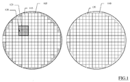
- FIG.1 there is schematically shown the structure obtained at an intermediate step of a production process of MEMS devices known in the state of the art.
- the MEMS devices are formed on two wafers, a sensor wafer 105 and a cap wafer 110, including a plurality of electronic sensors (each one of them defining a corresponding sensor chip 115 once cut) and a plurality of caps (each one of them defining a corresponding cap chip 120 for a sensor chip 115 once cut), respectively.
- the cap chips 120 are formed on the cap wafer 110 through the use of proper masks (not shown in the figure) in the one shot mode (that is, each mask covers a whole surface of the cap wafer 110). Instead, the sensor chips 115 are not formed on the wafer 105 in the one shot mode; in fact, the sensor chips 115, including electronic and mechanical circuits inside them, are more complex to implement than the cap chips 120 are, since they require a high integration capability.
- Such integration may not be effective if the wafer size increases, for the same process masks being used; the masks are then applied in an area 125 of the sensor wafer 105, which identifies a stepper: within each region 125 a subset of sensor chips 130 is formed according to the classic procedure (only nine shown in the figure for simplicity, but in very larger number in reality). Repeating such operations also for the other areas of the surface of the sensor wafer 105, it is obtained that on the whole surface of the sensor wafer 105 the desired plurality of sensor chips 115 will be formed.
- the cap wafer 110 is inverted and superimposed on the sensor wafer 105 (obtaining a composite wafer, not shown in the figure) so as to cover each sensor chip 115 with the corresponding cap chip 120; each cap chip 120 is then bonded to the corresponding sensor chip 115.
- the composite wafer being obtained from the union of the sensor wafer 105 with the cap wafer 110, is cut at each sensor chip 115, thus obtaining the desired MEMS devices.
- Each MEMS device is identified by an index that identifies the position of its sensor chip 115 in the sensor wafer 105, and thus also of its cap chip 120 in the cap wafer 110.
- such index is distributed partly on the sensor chip 115 and partly on the cap chip 120.
- each one of the sensor chip 115 and the cap chip 120 has a corresponding index portion, which takes an area of the chip 115, 120 being certainly lower than that taken by the whole index only on the sensor chip 115; therefore, the minimization of the size of the sensor chip 115, and hence of the whole MEMS device, is not penalized.
- the index portion being written on the cap chip 120 does not pose any problem of damage to the sensor chip 115 during the writing step.
- the solution according to the described embodiment of the invention facilitates the localization of the two index portions without the need of increasing the size of the sensor chip 115.
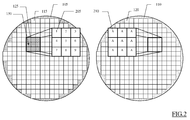
- FIG.2 there is shown, in a simplified way, an indexing method of the MEMS devices of FIG. 1 according to an embodiment of the present invention.
- first index portion 205 that identifies the sensor chip 115 within the corresponding area 125; in order to illustrate the invention conceptually, in FIG.2 such index is represented exemplarily by numbers (1, 2, 3, 4, 5, 6, 7, 8, 9) corresponding to the limited number (nine, precisely) of sensor chips 115 represented in an exemplary way in each area 125.
- Such first index portion 205 is the same for the sensor chips 115 (of the various subsets 130) that are located in the same position within the corresponding area 125.
- each cap chip 120 there is written a second index portion 210 (represented, for simplicity by letters A, B, C, and so on) being indicative of a position of the area 125 of the corresponding subset of the sensor chips 130 in the sensor wafer 105; such second index portion 210 is the same for the cap chips 120 whose sensor chips 115 of a same subset 130 are included in a same area 125. It is noted that since the composite wafer is obtained by overturning the cap wafer 110 and overlapping it to the sensor wafer 105, the second index portions 210 may be written in areas of the cap wafer 110 located in mirror positions with respect to the positions of the areas 125 in the sensor wafer 105.
- Each MEMS device is therefore identified by the first index portion 205 of its sensor chip 115 (indicating the position of the sensor chip 115 of the subset 130 within the corresponding area 125) and by the second index portion 210 of its cap chip 120 (indicating the position of the area 125 of the subset 130 of sensor chips within the sensor wafer 105).
- the index A4 will indicate the fourth sensor chip 115 of a specific area 125, B3 the third sensor chip 115 of another specific area 125, C1 the first sensor chip 115 of a further specific area 125, and so on.
- FIG.3 there is schematically shown an implementation of the indexing method of FIG.2 according to an embodiment of the present invention.
- FIG.3 there is shown an implementation of the indexing method of FIG.2 of the generic sensor chip 115 (leftward), and the corresponding cap chip 120 (both the sensor chip 105 and the cap chip 120 being depicted in a plant view for simplicity).
- the sensor chip 115 includes an active section 305 in which there is formed the electro-mechanical device, and a terminal section 310 in which there is formed a plurality of contacts (315a, 315b, 315c, 305 y-1 , 315 y ) being adapted to couple the active area 305 with an external device (not shown in the figure).
- the cap chip 120 covers the whole active section 305 (so as to protect the electro-mechanical device), but not the terminal section 310 (so as to leave uncovered the contacts 315a, 315b, 315c, 305 y-1 , 315 y ).
- the first index portion 205 on the sensor chip 115 is formed by a set of digits (for example, three); such digits are written in the terminal section 310, with each digit near a corresponding contact (for example, the first three contacts 315a, 315b, 315c).
- the first index portion 205 has the value 123 (for indicating the one-hundred-twenty-third sensor chip 115 in the corresponding area).
- the second index portion 210 on the cap chip 120 instead implements a (row and column) coordinates system being adapted to identify the position of the corresponding area of the sensor wafer.
- a row coordinate of the second index portion 210 is obtained from a row string 325 including a plurality of row dots (for example, 1,000 dots with a diameter of 5 ⁇ m and a spacing of 10 ⁇ m); the value of the row coordinate is defined in the string 325 by the position of a missing dot.
- a column coordinate is obtained from a column string 330 including a plurality of column dots: the value of the column coordinate is defined in the string 330 by the position of a missing point.
- both the row string 325 and the column string 330 have a missing dot in the position 2; therefore, the coordinates forming the second index portion 210 are (2;2), indicating the area in the second row and in the second column of the sensor wafer.
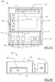
- FIG.4A and FIG.4B schematically show a MEMS device 400 implementing the indexing method described in FIG.3 at a step of a manufacturing process thereof; particularly, FIG.4A shows the MEMS device 400 in plant view and FIG.4B shows a cross-section view of the same MEMS device 400 along the IV-IV axis of FIG.4A .
- each cap chip 120 of the cap wafer is superimposed to the corresponding sensor chip 115 so as to cover it completely (in the following, only one sensor chip 115 and one cap chip 120 will be considered for simplicity, but it is clear that the MEMS devices are formed at a wafer level concurrently).
- a rear part of the cap chip 120 facing the sensor chip 115 is provided with two blind recesses 405 and 410; the recesses 405 and 410 are both formed (in the cap wafer) in a known manner at a proper step of the production process (e.g., before or after forming the second index portions 210).
- the recess 405 completely covers the active section 305 of the sensor chip 115, whereas the recess 410 completely covers the terminal section 310 thereof that include the contacts (whose only the contact 315b is visible) and the first index portion 205 - with the recess 410 that is deeper than the recess 405. Therefore, at such intermediate condition, only the second index portion 210 of the MEMS device 400 is visible (while the first index portion 205 is covered by the cap chip 120).
- a front of the cap chip 120 associated to the recess 410 is then subjected to a (known) localised Chemical Mechanical Polishing/Planarization operation (or other similar or equivalent operations) acting selectively thereon, until the 410 recess is opened.
- FIG.5A and FIG.5B schematically showing the same MEMS device 400 at another step of its manufacturing process in plant view and in cross-section view along the V-V axis of FIG.5A , respectively
- the terminals section 310 and the first index portion 205 of the sensor chip 115 are uncovered.
- the second index portion 210 is formed on the cap chip 120 after its planarization (at the level of the cap wafer).
- the MEMS device 400 thereby obtained is such that the index portion 205 formed in the sensor chip 115 and the index portion 210 formed in the cap chip 120 are both visible and detectable through known techniques - for example, by X-ray microscope reading.
- index portions 205, 210 distributed on two different chips 115, 120 are advantageous since such index portions 205, 210, being suitable to be located in arbitrary position within the corresponding chip 115, 120, are arranged in such a way to exploit pre-existing areas (possibly unused) of the chip 115, 120 without the excessive length of the index being incompatible with the demands of miniaturization of the MEMS device 400. In this way, the minimizing of the size of the chips 115, 120, and hence of the whole MEMS device 400, is not penalized.
- FIG.6A and 6B there is shown an implementation of the indexing method of FIG.2 according to another embodiment of the present invention.
- FIG.6A there is again shown the sensor wafer 105 with a plurality of sensor chips 115 that are arranged in the sensor wafer 105 in another manner known in the state of the art.
- Such embodiment differs from that shown in FIG.3 substantially by the different mutual orientation of two (or more) adjacent sensor chips 115.
- the sensor chips are distributed on the sensor wafer 105 in such a way that each sensor chip 115 is rotated by 180° with respect to the immediately preceding sensor chip and the immediately following sensor chip, and with respect to the sensor chip immediately above and the sensor chip immediately below.
- the sensor chip 115 is rotated by 180° with respect to the adjacent sensor chip 115' below it (hereinafter, the components of the sensor chip 115' are indicated with the same references of the corresponding components of the sensor chip 115 with the addition of an apex).
- Such structure is commonly implemented for avoiding possible breakages of the sensor wafer 105; in fact, since the sensor chips 115, 115' have areas of different weight (the active section 305, 305', the terminal section 310, 310' and an unused area), an identical arrangement of the sensor chips 115, 115' on the sensor wafer 105 may cause structural damages of the sensor wafer 105 itself since the weight of all the sensor chips 115, 115' is not distributed uniformly on the sensor wafer 105 but it is concentrated in certain areas thereof.
- first index portion 205 on first three contacts 315a, 315b, 315c of the sensor chip 115 (in the sensor wafer 105, from left to right, at the top), and a first index portion 205' having the same digits of the first index portion 205 on first three contacts 315a', 315b', 315c' of the sensor chip 115' (in mirrored position in the sensor wafer 105, from right to left, at the bottom).
- the reading of the index is performed by placing the sensor chip 115, 115' with the corresponding terminals section 310, 310' oriented downward; in this way, the sensor chip 115 is marked by the index portion 205 (on the first three contacts 315a, 315b, 315c) having value 123, so that it will be read as the one-hundred-twenty-third sensor chip 115 within the corresponding area of the sensor wafer 105; instead, the sensor chip 115' is marked by the index portion 205', which is in the same position on the first three contacts 315a', 315b', 315c' once arranged according to the predefined common orientation chosen for the reading of the index.
- the index portion 205' has again the value 123, but with the corresponding digits over-turned vertically; therefore, such value will be read as a different position of the sensor chip 105' within the corresponding area of the sensor wafer 105 (for example, equal to the value of the index portion 205 added to the half of the sensor chips formed within the area of the sensor wafer 105).
- each index including at least two possible orientations, allows indexing at least two electronic devices.
- the solution according to an embodiment of the invention lends itself to be implemented with an equivalent method (by using similar steps, removing some steps being non-essential, or adding further optional steps); moreover, the steps may be performed in a different order, concurrently or in an interleaved way (at least in part). Particularly, nothing prevents from forming the sensors chips and the cap chips directly (by dicing the sensor wafer and the cap wafer, respectively), and then coupling each cap chip with the corresponding sensor chip individually.
- the electronic device includes more than two chips coupled to each other (each one, or some but not all of them, including a corresponding index portion).
- index portions implement a different coordinate system, for example a mapping of the chip, or if such coordinates are written with non-alphanumeric characters, for example using Morse or Braille codes.
- index portions are formed by numerical characters in a non-decimal base (for example, in hexadecimal base), or by alphanumeric characters, including, for example, the ten numbers form 0 to 9 and the twenty-one letters from A to Z, for increasing the number of indexable devices.
- the index may be distributed on two chips in any other way (for example, in case of an index that identifies the absolute position of the chip in the wafer, it is possible to write its most significant digits on a chip and its least significant digits on the other chip).
- the proposed solution lends itself to be applied to any other type of electronic device (including electronic devices being not of the MEMS type).
- the index portions may be arranged on more free areas of the chip in order to maximize the exploitation of the area of the chip and to avoid possible damages of the contacts when writing the index.
- the indexes may also be not directly visible; in this case, the indexes are read with non-optical techniques (for example, echo-techniques when they are defined by corresponding notches).
- the electronic device in a different way. For example, nothing prevents removing part of the cap wafer with other techniques, or forming the recesses with different shape, size and/or depth (for example, with the recesses that may have the same depth when a localized planarization operation is performed).
- same index portions with different reciprocal orientation may be applied to groups of more chips (for example, four); similarly, same index portions may be diversified by other orientations of the digits included therein (for example, by overturning the digits by 90°, 180° and 270° on different chips), or by combinations thereof.
- the electronic devices have a different structure or include equivalent components (either separately or in combination to each other).
- the proposed solution is not limited to the material of the wafer (in this case, silicon), but it may be applied to chips made on substrates of any other material (for example, quartz and plastic).
- the proposed structure might be part of the design of an integrated circuit.
- the design may also be created in a programming language; moreover, if the designer does not fabricate chips or masks, the design may be transmitted by physical means to others.
- the resulting integrated circuit may be distributed by its manufacturer in raw wafer form, as a bare die, or in packages.
- the proposed electronic device may be mounted in intermediate products (such as mother boards) and coupled with one or more other chips (such as a processor or a memory).
- the integrated circuit is suitable to be used in complex systems (such as logic computers).
Landscapes
- Micromachines (AREA)
- Pressure Sensors (AREA)
Abstract

Description
- The solution according to one or more embodiments of the present invention generally relates to electronic devices, in particular, such solution relates to the indexing of the electronic devices.
- Electronic devices are typically integrated in chips of semiconductor material. The chips are formed in large numbers in a wafer of semiconductor material through a production process typically performed in a sequence of steps. At the end of this process, the wafer includes a plurality of chips (equal to each other) that are then separated by a cutting operation.
- In particular, some classes of electronic devices are formed by two chips coupled to each other.
- For example, a MEMS (Micro-Electro-Mechanical System) device is formed by a sensor chip, wherein there is implemented an electro-mechanical sensor, and by a cap chip, used to cover the sensor in order to protect it form the external environment.
- The production process of such class of electronic devices involves the formation of a plurality of sensor chips on a wafer, and the formation of a corresponding plurality of cap chips on another wafer. A composite wafer is obtained from the union of these two wafers by overlapping them. The MEMS devices are then obtained by cutting the composite wafer at each pair of sensor chip and cap chip.
- Should the MEMS devices be found defective before or during their use, they are returned to the manufacturer in order to carry out a failure analysis; therefore, the possibility of tracing the original position of the sensor chip in the corresponding wafer is of strategic importance for the management of the quality of the production process. In fact, functional parameters, performance and reliability of each sensor chip may vary even considerably as a function of its position in the wafer. For this reason, it is important for the manufacturer to know where to intervene for improving the quality of the production process.
- For such purpose, it is known in the state of the art to provide on each sensor chip an index being indicative of its position within the corresponding wafer.
- In particular, with the increase of the size of the wafers and with the increase of the integration capability of the electronic devices, each step of the production process of the sensor chips through a proper photolithographic mask may no more be performed in only one step (so-called "one shot" mode) over the entire area of the wafer, but it is typically performed step by step (so-called "stepper shot" mode) on different portions of the wafer; at each step, the mask acts on a corresponding area of the wafer wherein there will be made, at the end of the process, a corresponding subset of sensor chips; the same operation is repeated until applying the same mask on the entire area of the wafer. In this case, the index of each sensor chip is formed by two portions. A first index portion (obtained through a specific mask) identifies the position of the sensor chip within the corresponding area of the wafer (being equal for the sensor chips placed in corresponding positions in the different areas because of the repeated use of the same mask). A second portion of the index (obtained by known techniques of direct writing on wafer, for example, laser-based) then identifies the area of the wafer in which the sensor chip is formed.
- In any case, the integration capability of the sensor chips required by the current design specifications is such that the number of sensor chips integrated in each wafer grows significantly; therefore, the number of sensor chips to be indexed being greater and greater, the index will be longer and longer. However, an increasing length of the index is obviously inconsistent with the miniaturization of the electronic devices because the length of the index may significantly affect the size of the sensor chips and, ultimately, of the corresponding electronic devices.
- The problem is exacerbated by the fact that often, for facilitating the identification of the index portions, it is preferred to write the two index portions in different regions of the sensor chip. Since such regions must be properly spaced from the active areas of the sensor chip for avoiding damages during the writing of the index, this technique causes further increases in the size of the electronic devices.
- Other indexing techniques are known in the art.
- For example, the document
JP 2007 081123 - The document
US 2003/166313 discloses a semiconductor element mounting method providing for the possibility of superimposing different chips to each other at a wafer level. - The document
US 2003/127718 discloses a semiconductor component and a method for identifying a semiconductor component that comprises at least one semiconductor substrate equipped with electronic/electromechanical components, which semiconductor substrate - except for its leads - is embedded in a housing part made of plastic. - The document
WO 01/39269 - In its general terms, the solution according to one or more embodiments of the present invention is based on the idea of distributing the index on different chips concurring to the formation of the electronic devices.
- In particular, several aspects of the solution according to an embodiment of the invention are set forth in the independent claims. Advantageous features of the same solution are indicated in the dependent claims.
- More specifically, one aspect of the solution according to an embodiment of the invention proposes a method for indexing electronic devices. The method includes the steps of forming a plurality of first chips in a first wafer, forming a plurality of seconds chips in a second wafer, forming the electronic devices by coupling each first chip with a corresponding second chip, and forming an index on each electronic device; the index is indicative of a position of the corresponding first chip in the first wafer. In the solution according to an embodiment of the invention, the step of forming an index includes forming a first portion of the index on the first chip, and forming a second portion of the index on the second chip.
- Another aspect of the solution according to an embodiment of the invention proposes a corresponding electronic device.
- The solution according to one or more embodiments of the invention, as well as further features and the advantages thereof, will be best understood with reference to the following detailed description, given purely by way of a non-restrictive indication, to be read in conjunction with the accompanying drawings (wherein corresponding elements are denoted with equal or similar references, and their explanation is not repeated for the sake of exposition brevity). In this regard, it is expressly intended that the figures are not necessarily drawn to scale and that, unless otherwise indicated, they are simply used to conceptually illustrate the described structures and procedures. In particular:
-
FIG.1 schematically shows the structure obtained at an intermediate step of a production process of MEMS devices known in the state of the art; -
FIG.2 shows, in a simplified way, an indexing method of the MEMS devices of FIG. according to an embodiment of the present invention; -
FIG.3 schematically shows an implementation of the indexing method ofFIG.2 according to an embodiment of the present invention; -
FIG.4A and FIG.4B schematically show a plant view and a cross-section view, respectively, of a MEMS device implementing the indexing method described inFIG.3 at a step of a manufacturing process thereof; -
FIG.5A and FIG.5B schematically show a plant view and a cross-section view, respectively, of the MEMS device ofFIG.4A at another step of a manufacturing process thereof; and -
FIG.6A and 6B schematically show an implementation of the indexing method ofFIG.2 according to another embodiment of the invention. - Considering in particular
FIG.1 , there is schematically shown the structure obtained at an intermediate step of a production process of MEMS devices known in the state of the art. In particular, the MEMS devices are formed on two wafers, asensor wafer 105 and acap wafer 110, including a plurality of electronic sensors (each one of them defining acorresponding sensor chip 115 once cut) and a plurality of caps (each one of them defining acorresponding cap chip 120 for asensor chip 115 once cut), respectively. - The
cap chips 120 are formed on the cap wafer 110 through the use of proper masks (not shown in the figure) in the one shot mode (that is, each mask covers a whole surface of the cap wafer 110). Instead, thesensor chips 115 are not formed on thewafer 105 in the one shot mode; in fact, thesensor chips 115, including electronic and mechanical circuits inside them, are more complex to implement than thecap chips 120 are, since they require a high integration capability. Such integration may not be effective if the wafer size increases, for the same process masks being used; the masks are then applied in anarea 125 of thesensor wafer 105, which identifies a stepper: within each region 125 a subset ofsensor chips 130 is formed according to the classic procedure (only nine shown in the figure for simplicity, but in very larger number in reality). Repeating such operations also for the other areas of the surface of thesensor wafer 105, it is obtained that on the whole surface of the sensor wafer 105 the desired plurality ofsensor chips 115 will be formed. - At this point, the
cap wafer 110 is inverted and superimposed on the sensor wafer 105 (obtaining a composite wafer, not shown in the figure) so as to cover eachsensor chip 115 with thecorresponding cap chip 120; eachcap chip 120 is then bonded to thecorresponding sensor chip 115. - Then, the composite wafer, being obtained from the union of the
sensor wafer 105 with thecap wafer 110, is cut at eachsensor chip 115, thus obtaining the desired MEMS devices. - Each MEMS device is identified by an index that identifies the position of its
sensor chip 115 in thesensor wafer 105, and thus also of itscap chip 120 in thecap wafer 110. - In the solution according to an embodiment of the present invention (as described in detail below) such index is distributed partly on the
sensor chip 115 and partly on thecap chip 120. - In this way, each one of the
sensor chip 115 and thecap chip 120 has a corresponding index portion, which takes an area of thechip sensor chip 115; therefore, the minimization of the size of thesensor chip 115, and hence of the whole MEMS device, is not penalized. - Furthermore, the index portion being written on the
cap chip 120 does not pose any problem of damage to thesensor chip 115 during the writing step. - Finally, the solution according to the described embodiment of the invention facilitates the localization of the two index portions without the need of increasing the size of the
sensor chip 115. - Turning now to
FIG.2 , there is shown, in a simplified way, an indexing method of the MEMS devices ofFIG. 1 according to an embodiment of the present invention. - On each
sensor chip 115 there is written afirst index portion 205 that identifies thesensor chip 115 within thecorresponding area 125; in order to illustrate the invention conceptually, inFIG.2 such index is represented exemplarily by numbers (1, 2, 3, 4, 5, 6, 7, 8, 9) corresponding to the limited number (nine, precisely) ofsensor chips 115 represented in an exemplary way in eacharea 125. Suchfirst index portion 205 is the same for the sensor chips 115 (of the various subsets 130) that are located in the same position within thecorresponding area 125. - On each
cap chip 120 there is written a second index portion 210 (represented, for simplicity by letters A, B, C, and so on) being indicative of a position of thearea 125 of the corresponding subset of thesensor chips 130 in thesensor wafer 105; suchsecond index portion 210 is the same for thecap chips 120 whosesensor chips 115 of asame subset 130 are included in asame area 125. It is noted that since the composite wafer is obtained by overturning thecap wafer 110 and overlapping it to thesensor wafer 105, thesecond index portions 210 may be written in areas of thecap wafer 110 located in mirror positions with respect to the positions of theareas 125 in thesensor wafer 105. - Each MEMS device is therefore identified by the
first index portion 205 of its sensor chip 115 (indicating the position of thesensor chip 115 of thesubset 130 within the corresponding area 125) and by thesecond index portion 210 of its cap chip 120 (indicating the position of thearea 125 of thesubset 130 of sensor chips within the sensor wafer 105). For example, the index A4 will indicate thefourth sensor chip 115 of aspecific area 125, B3 thethird sensor chip 115 of anotherspecific area 125, C1 thefirst sensor chip 115 of a furtherspecific area 125, and so on. - Turning now to
FIG.3 , there is schematically shown an implementation of the indexing method ofFIG.2 according to an embodiment of the present invention. - In particular, in
FIG.3 there is shown an implementation of the indexing method ofFIG.2 of the generic sensor chip 115 (leftward), and the corresponding cap chip 120 (both thesensor chip 105 and thecap chip 120 being depicted in a plant view for simplicity). - The
sensor chip 115 includes anactive section 305 in which there is formed the electro-mechanical device, and aterminal section 310 in which there is formed a plurality of contacts (315a, 315b, 315c, 305y-1, 315y) being adapted to couple theactive area 305 with an external device (not shown in the figure). - In a known manner, the
cap chip 120 covers the whole active section 305 (so as to protect the electro-mechanical device), but not the terminal section 310 (so as to leave uncovered thecontacts - The
first index portion 205 on thesensor chip 115 is formed by a set of digits (for example, three); such digits are written in theterminal section 310, with each digit near a corresponding contact (for example, the first threecontacts first index portion 205 has the value 123 (for indicating the one-hundred-twenty-third sensor chip 115 in the corresponding area). - The
second index portion 210 on thecap chip 120 instead implements a (row and column) coordinates system being adapted to identify the position of the corresponding area of the sensor wafer. - A row coordinate of the
second index portion 210 is obtained from arow string 325 including a plurality of row dots (for example, 1,000 dots with a diameter of 5µm and a spacing of 10µm); the value of the row coordinate is defined in thestring 325 by the position of a missing dot. - Similarly, a column coordinate is obtained from a
column string 330 including a plurality of column dots: the value of the column coordinate is defined in thestring 330 by the position of a missing point. - In the example in the figure, both the
row string 325 and thecolumn string 330 have a missing dot in theposition 2; therefore, the coordinates forming thesecond index portion 210 are (2;2), indicating the area in the second row and in the second column of the sensor wafer. -
FIG.4A and FIG.4B schematically show aMEMS device 400 implementing the indexing method described inFIG.3 at a step of a manufacturing process thereof; particularly,FIG.4A shows theMEMS device 400 in plant view andFIG.4B shows a cross-section view of thesame MEMS device 400 along the IV-IV axis ofFIG.4A . In this phase, eachcap chip 120 of the cap wafer is superimposed to thecorresponding sensor chip 115 so as to cover it completely (in the following, only onesensor chip 115 and onecap chip 120 will be considered for simplicity, but it is clear that the MEMS devices are formed at a wafer level concurrently). As can be seen, a rear part of thecap chip 120 facing thesensor chip 115 is provided with twoblind recesses recesses recess 405 completely covers theactive section 305 of thesensor chip 115, whereas therecess 410 completely covers theterminal section 310 thereof that include the contacts (whose only thecontact 315b is visible) and the first index portion 205 - with therecess 410 that is deeper than therecess 405. Therefore, at such intermediate condition, only thesecond index portion 210 of theMEMS device 400 is visible (while thefirst index portion 205 is covered by the cap chip 120). - A front of the
cap chip 120 associated to therecess 410 is then subjected to a (known) localised Chemical Mechanical Polishing/Planarization operation (or other similar or equivalent operations) acting selectively thereon, until the 410 recess is opened. - In this way, as visible in
FIG.5A and FIG.5B (schematically showing thesame MEMS device 400 at another step of its manufacturing process in plant view and in cross-section view along the V-V axis ofFIG.5A , respectively) theterminals section 310 and thefirst index portion 205 of thesensor chip 115 are uncovered. - Alternatively, it is possible to perform the Chemical Mechanical Polishing/Planarization operation on the whole cap wafer (thus making the production process easier), by stopping it (after the
recess 410 has been opened) before reaching therecess 405. In this case, thesecond index portion 210 is formed on thecap chip 120 after its planarization (at the level of the cap wafer). - Anyway, regardless of the disclosed exemplary and not limiting production processes being usable to make the
MEMS device 400, theMEMS device 400 thereby obtained is such that theindex portion 205 formed in thesensor chip 115 and theindex portion 210 formed in thecap chip 120 are both visible and detectable through known techniques - for example, by X-ray microscope reading. - The use of an index formed by two
portions different chips such index portions corresponding chip chip MEMS device 400. In this way, the minimizing of the size of thechips whole MEMS device 400, is not penalized. - In
FIG.6A and 6B there is shown an implementation of the indexing method ofFIG.2 according to another embodiment of the present invention. - In particular, in
FIG.6A there is again shown thesensor wafer 105 with a plurality ofsensor chips 115 that are arranged in thesensor wafer 105 in another manner known in the state of the art. - Such embodiment differs from that shown in
FIG.3 substantially by the different mutual orientation of two (or more) adjacent sensor chips 115. The sensor chips are distributed on thesensor wafer 105 in such a way that eachsensor chip 115 is rotated by 180° with respect to the immediately preceding sensor chip and the immediately following sensor chip, and with respect to the sensor chip immediately above and the sensor chip immediately below. In particular, as shown inFIG.6A for a generic andexemplary pair 505 ofsensor chips 115 and 115', thesensor chip 115 is rotated by 180° with respect to the adjacent sensor chip 115' below it (hereinafter, the components of the sensor chip 115' are indicated with the same references of the corresponding components of thesensor chip 115 with the addition of an apex). Such structure is commonly implemented for avoiding possible breakages of thesensor wafer 105; in fact, since thesensor chips 115, 115' have areas of different weight (theactive section 305, 305', theterminal section 310, 310' and an unused area), an identical arrangement of thesensor chips 115, 115' on thesensor wafer 105 may cause structural damages of thesensor wafer 105 itself since the weight of all thesensor chips 115, 115' is not distributed uniformly on thesensor wafer 105 but it is concentrated in certain areas thereof. - In such case, in an embodiment of the invention, it is possible to write a
first index portion 205 on first threecontacts sensor wafer 105, from left to right, at the top), and a first index portion 205' having the same digits of thefirst index portion 205 on first threecontacts 315a', 315b', 315c' of the sensor chip 115' (in mirrored position in thesensor wafer 105, from right to left, at the bottom). - During reading of the index on the
sensor chips 115 and 115' being formed by cutting eachpair 505 along its own axis (dashed line inFIG.6A ), an arbitrary predefined common orientation is assumed, as shown inFIG.6B . In the example in the figure, the reading of the index is performed by placing thesensor chip 115, 115' with thecorresponding terminals section 310, 310' oriented downward; in this way, thesensor chip 115 is marked by the index portion 205 (on the first threecontacts third sensor chip 115 within the corresponding area of thesensor wafer 105; instead, the sensor chip 115' is marked by the index portion 205', which is in the same position on the first threecontacts 315a', 315b', 315c' once arranged according to the predefined common orientation chosen for the reading of the index. The index portion 205' has again the value 123, but with the corresponding digits over-turned vertically; therefore, such value will be read as a different position of the sensor chip 105' within the corresponding area of the sensor wafer 105 (for example, equal to the value of theindex portion 205 added to the half of the sensor chips formed within the area of the sensor wafer 105). - The proposed solution is advantageous since the use of over-turned alphanumeric characters allows achieving a doubling of the number of indexable electronic devices with the same number of characters: in particular, each index, including at least two possible orientations, allows indexing at least two electronic devices.
- Naturally, in order to satisfy local and specific requirements, a person skilled in the art may apply to the solution described above many logical and/or physical modifications and alterations. More specifically, although the present invention has been described with a certain degree of particularity with reference to preferred embodiment(s) thereof, it should be understood that various omissions, substitutions and changes in the form and details as well as other embodiments are possible; moreover, it is expressly intended that specific elements and/or method steps described in connection with any disclosed embodiment of the invention may be incorporated in any other embodiment as a matter of general design choice.
- For example, the solution according to an embodiment of the invention lends itself to be implemented with an equivalent method (by using similar steps, removing some steps being non-essential, or adding further optional steps); moreover, the steps may be performed in a different order, concurrently or in an interleaved way (at least in part). Particularly, nothing prevents from forming the sensors chips and the cap chips directly (by dicing the sensor wafer and the cap wafer, respectively), and then coupling each cap chip with the corresponding sensor chip individually.
- Similar considerations apply if the index includes more than two portions, properly distributed on the two chips.
- Moreover, nothing prevents that the electronic device includes more than two chips coupled to each other (each one, or some but not all of them, including a corresponding index portion).
- The same considerations apply if the index portions implement a different coordinate system, for example a mapping of the chip, or if such coordinates are written with non-alphanumeric characters, for example using Morse or Braille codes.
- Nothing prevents that the index portions are formed by numerical characters in a non-decimal base (for example, in hexadecimal base), or by alphanumeric characters, including, for example, the ten numbers form 0 to 9 and the twenty-one letters from A to Z, for increasing the number of indexable devices.
- The index may be distributed on two chips in any other way (for example, in case of an index that identifies the absolute position of the chip in the wafer, it is possible to write its most significant digits on a chip and its least significant digits on the other chip).
- Although the proposed solution has been described with reference to electronic devices whose chips are formed one in stepper shot mode and the other in one shot mode, this should not be interpreted in a limitative way (with the same solution that may be applied even when the two chips are both formed in stepper shot or one shot mode). Moreover, such solution may be applied even in case of use of different lithographic techniques.
- The proposed solution lends itself to be applied to any other type of electronic device (including electronic devices being not of the MEMS type).
- The same considerations apply if the arrangement of the index portions is different; for example, they may be arranged on more free areas of the chip in order to maximize the exploitation of the area of the chip and to avoid possible damages of the contacts when writing the index. Alternatively, the indexes (or parts thereof) may also be not directly visible; in this case, the indexes are read with non-optical techniques (for example, echo-techniques when they are defined by corresponding notches).
- In any case, it is possible to produce the electronic device in a different way. For example, nothing prevents removing part of the cap wafer with other techniques, or forming the recesses with different shape, size and/or depth (for example, with the recesses that may have the same depth when a localized planarization operation is performed). Alternatively, it is also possible to form a through-hole on each cap chip (when in the cap wafer), so as to leave the terminals section of the corresponding sensor chip directly uncovered when the cap wafer is coupled with the sensor wafer.
- The feature of using same index portions with different reciprocal orientation may be applied to groups of more chips (for example, four); similarly, same index portions may be diversified by other orientations of the digits included therein (for example, by overturning the digits by 90°, 180° and 270° on different chips), or by combinations thereof.
- Similar considerations apply if the electronic devices have a different structure or include equivalent components (either separately or in combination to each other). In particular, the proposed solution is not limited to the material of the wafer (in this case, silicon), but it may be applied to chips made on substrates of any other material (for example, quartz and plastic).
- It should be readily apparent that the proposed structure might be part of the design of an integrated circuit. The design may also be created in a programming language; moreover, if the designer does not fabricate chips or masks, the design may be transmitted by physical means to others. In any case, the resulting integrated circuit may be distributed by its manufacturer in raw wafer form, as a bare die, or in packages. Moreover, the proposed electronic device may be mounted in intermediate products (such as mother boards) and coupled with one or more other chips (such as a processor or a memory). In any case, the integrated circuit is suitable to be used in complex systems (such as logic computers).
Claims (15)
- A method for indexing electronic devices (400), the method including the steps of:forming a plurality of first chips (115) in a first wafer (105),forming a plurality of second chips (120) in a second wafer (110),forming a plurality of electronic devices by coupling each first chip with a corresponding second chip, andforming an index on each electronic device, the index being indicative of a position of the corresponding first chip in the first wafer,characterized in that
the step of forming an index includes:forming a first portion (205) of the index on the first chip, andforming a second portion (210) of the index on the second chip. - The method according to claim 1, wherein the first wafer includes a plurality of equal areas (125) each one including a subset (130) of the first chips, the first portion of the index being indicative of a position of the first chip in the corresponding area (125) and the second portion of the index being indicative of a position of the corresponding area (125) in the first wafer.
- The method according to claim 2, wherein the step of forming a plurality of first chips includes:forming the first chips of each subset concurrently in the corresponding area, the subsets being formed in succession in the first wafer,wherein the step of forming a plurality of second chips includes:forming the second chips concurrently in the second wafer,wherein the step of forming a plurality of electronic devices includes:forming a composite wafer by joining each first chip of the first wafer to the corresponding second chip of the second wafer, andforming each electronic device by cutting the corresponding joined first chip and second chip from the composite wafer,wherein the step of forming a first portion of the index includes:forming the first portions of the indexes on the first chips of each subset concurrently, the first portions of the indexes of the subsets being formed in succession in the first wafer, andwherein the step of forming a second portion of the index includes:forming the second portions of the indexes on the second chips concurrently in the second wafer.
- The method according to any of the preceding claims, wherein each electronic device is a Micro-Electro-Mechanical device, the first chip of the electronic device including sensor means (115) and the second chip of the electronic device including a cover (120) for protecting the sensor means.
- The method according to any of the preceding claims, wherein for each electronic device the second chip covers a functional area (305) of the first chip, the first portion of the index being included in a terminal area (310) of the first chip being not covered by the second chip.
- The method according to claim 5, wherein the step of forming a plurality of electronic devices includes:forming a recess (405) and a further recess (410) on each second chip (120) in the second wafer (110),coupling the first wafer (105) with the second wafer, the recess and the further recess of each second chip covering the functional area (305) and the terminal area (310), respectively, of the corresponding first chip, andremoving part of the second wafer until reaching the further recess (410) of each second chip (120) thereby uncovering the terminal area (310) of the corresponding first chip.
- The method according to claim 6, wherein the step of removing part of the second wafer is localised to selectively remove part of each second chip associated with the corresponding further recess (410).
- The method according to claim 6, wherein each further recess (410) is deeper than each recess (405), the step of removing part of the second wafer including planarizing the second wafer without reaching the recess (405), the step of forming a second portion (210) of the index on the second chip being performed after said planarizing of the second wafer.
- The method according to any of the preceding claims,
wherein the step of forming a plurality of first chips includes:forming the first chips in groups (500), the first chips of each group having a different orientation in the first wafer; andwherein the step of forming a first portion of the index includes:forming the first portion of the index on the first chips of each group with a common value, the first portion of the index of the first chips of the group being formed with reciprocal different orientations with respect to a common reading reference of the first chips of the group. - The method according to claim 9, wherein the step of forming the first chips in groups (500), includes:forming the first chips in pairs of two first chips, the two first chips of each pair being rotated by 180° with respect to each other.
- The method according to claim 9 or 10, wherein the first portion of the index includes at least one digit, the step of forming the first portion of the index on the first chips of each group including:forming each digit of the first portion of the index on each first chip of the group overturned with respect to the corresponding digit of each other first chip of the group.
- The method according to any claim from 9 to 11, wherein the common reading reference of the first chips includes a set of contacts of each first chip.
- An electronic device (400) including a first chip (115), a second chip (120) coupled with the first chip, and an index of the first chip,
characterized in that
the index includes a first portion (205) on the first chip and a second portion (210) on the second chip. - The electronic device according to claim 13, wherein the electronic device is a Micro-Electro-Mechanical device, the first chip including sensor means (115) and the second chip including a cover (120) for protecting the sensor means.
- The electronic device according to claims 13 or 14, wherein the first portion of the index is defined by a value thereof and an orientation thereof with respect to a common reading reference of the first chips.
Applications Claiming Priority (1)
| Application Number | Priority Date | Filing Date | Title |
|---|---|---|---|
| ITMI20091684 | 2009-09-30 |
Publications (2)
| Publication Number | Publication Date |
|---|---|
| EP2306517A1 true EP2306517A1 (en) | 2011-04-06 |
| EP2306517B1 EP2306517B1 (en) | 2016-11-02 |
Family
ID=41571746
Family Applications (1)
| Application Number | Title | Priority Date | Filing Date |
|---|---|---|---|
| EP10184411.6A Active EP2306517B1 (en) | 2009-09-30 | 2010-09-30 | Indexing of electronic devices using marks distributed on two coupled chips |
Country Status (1)
| Country | Link |
|---|---|
| EP (1) | EP2306517B1 (en) |
Citations (5)
| Publication number | Priority date | Publication date | Assignee | Title |
|---|---|---|---|---|
| WO2001039269A1 (en) | 1999-11-24 | 2001-05-31 | Micronic Laser Systems Ab | Method and apparatus for personalization of semiconductor |
| US20030127718A1 (en) | 2000-08-10 | 2003-07-10 | Frieder Haag | Semiconductor component and a method for identifying a semiconductor component |
| US20030166313A1 (en) | 2001-09-26 | 2003-09-04 | Hidenobu Nishikawa | Semiconductor element mounting method |
| JP2007048989A (en) * | 2005-08-11 | 2007-02-22 | Renesas Technology Corp | Semiconductor device and marking method thereof |
| JP2007081123A (en) | 2005-09-14 | 2007-03-29 | Toshiba Corp | Method for forming semiconductor device |
Family Cites Families (2)
| Publication number | Priority date | Publication date | Assignee | Title |
|---|---|---|---|---|
| JPH04340214A (en) * | 1990-12-14 | 1992-11-26 | Fujitsu Ltd | Manufacture of semiconductor device |
| EP1135794B1 (en) * | 1998-12-04 | 2008-04-23 | FormFactor, Inc. | A method and apparatus for the transport and tracking of an electronic component |
-
2010
- 2010-09-30 EP EP10184411.6A patent/EP2306517B1/en active Active
Patent Citations (5)
| Publication number | Priority date | Publication date | Assignee | Title |
|---|---|---|---|---|
| WO2001039269A1 (en) | 1999-11-24 | 2001-05-31 | Micronic Laser Systems Ab | Method and apparatus for personalization of semiconductor |
| US20030127718A1 (en) | 2000-08-10 | 2003-07-10 | Frieder Haag | Semiconductor component and a method for identifying a semiconductor component |
| US20030166313A1 (en) | 2001-09-26 | 2003-09-04 | Hidenobu Nishikawa | Semiconductor element mounting method |
| JP2007048989A (en) * | 2005-08-11 | 2007-02-22 | Renesas Technology Corp | Semiconductor device and marking method thereof |
| JP2007081123A (en) | 2005-09-14 | 2007-03-29 | Toshiba Corp | Method for forming semiconductor device |
Also Published As
| Publication number | Publication date |
|---|---|
| EP2306517B1 (en) | 2016-11-02 |
Similar Documents
| Publication | Publication Date | Title |
|---|---|---|
| JP4257844B2 (en) | Semiconductor device and manufacturing method thereof | |
| US10109590B2 (en) | Indexing of electronic devices distributed on different chips | |
| JP5184003B2 (en) | Semiconductor integrated circuit and dummy pattern arrangement method | |
| US7947563B2 (en) | Chip ID applying method suitable for use in semiconductor integrated circuit | |
| CN100555622C (en) | Semiconductor chip with identification code, manufacturing method and management system thereof | |
| KR20210035914A (en) | A semiconductor wafer alignment marking method and a semiconductor package having alignment marking portions | |
| CN115443520B (en) | Methods for identifying grains, wafers, and the location of grains on wafers | |
| CN1866492B (en) | System and method for identification of a reference integrated circuit for a pick-and-place equipment | |
| EP2168155B1 (en) | Integrated circuits on a wafer and methods for manufacturing integrated circuits | |
| EP2306517B1 (en) | Indexing of electronic devices using marks distributed on two coupled chips | |
| EP2168156B1 (en) | Integrated circuits on a wafer and methods for manufacturing integrated circuits | |
| JP4292041B2 (en) | Semiconductor substrate, semiconductor substrate manufacturing method, and semiconductor device manufacturing method | |
| CN111415881A (en) | Chip marking method, wafer and chip | |
| JP4506780B2 (en) | Manufacturing method of semiconductor substrate | |
| US12005711B2 (en) | Manufacturing method of narrow type inkjet print head chip | |
| JP6066693B2 (en) | Electronic devices | |
| JPS62235952A (en) | Mask for semiconductor device | |
| JP4572564B2 (en) | Semiconductor device | |
| JP2007116203A (en) | Manufacturing method of semiconductor device | |
| KR100388298B1 (en) | Substrate for semiconductor package | |
| JP4830402B2 (en) | Manufacturing method of semiconductor device | |
| KR20060026191A (en) | Printed Circuit Board with Solder Mask Eccentric Mark | |
| JPH0219976B2 (en) | ||
| CN119069361A (en) | A framework packaging method, system, intelligent terminal and storage medium | |
| KR20090098066A (en) | Substrate for semiconductor package and manufacturing method of semiconductor package using same |
Legal Events
| Date | Code | Title | Description |
|---|---|---|---|
| PUAI | Public reference made under article 153(3) epc to a published international application that has entered the european phase |
Free format text: ORIGINAL CODE: 0009012 |
|
| AK | Designated contracting states |
Kind code of ref document: A1 Designated state(s): AL AT BE BG CH CY CZ DE DK EE ES FI FR GB GR HR HU IE IS IT LI LT LU LV MC MK MT NL NO PL PT RO SE SI SK SM TR |
|
| AX | Request for extension of the european patent |
Extension state: BA ME RS |
|
| 17P | Request for examination filed |
Effective date: 20111006 |
|
| RAP1 | Party data changed (applicant data changed or rights of an application transferred) |
Owner name: STMICROELECTRONICS SRL |
|
| 17Q | First examination report despatched |
Effective date: 20120918 |
|
| GRAP | Despatch of communication of intention to grant a patent |
Free format text: ORIGINAL CODE: EPIDOSNIGR1 |
|
| INTG | Intention to grant announced |
Effective date: 20160527 |
|
| GRAS | Grant fee paid |
Free format text: ORIGINAL CODE: EPIDOSNIGR3 |
|
| GRAA | (expected) grant |
Free format text: ORIGINAL CODE: 0009210 |
|
| AK | Designated contracting states |
Kind code of ref document: B1 Designated state(s): AL AT BE BG CH CY CZ DE DK EE ES FI FR GB GR HR HU IE IS IT LI LT LU LV MC MK MT NL NO PL PT RO SE SI SK SM TR |
|
| REG | Reference to a national code |
Ref country code: GB Ref legal event code: FG4D |
|
| REG | Reference to a national code |
Ref country code: AT Ref legal event code: REF Ref document number: 842612 Country of ref document: AT Kind code of ref document: T Effective date: 20161115 Ref country code: CH Ref legal event code: EP |
|
| REG | Reference to a national code |
Ref country code: IE Ref legal event code: FG4D |
|
| REG | Reference to a national code |
Ref country code: DE Ref legal event code: R096 Ref document number: 602010037590 Country of ref document: DE |
|
| PG25 | Lapsed in a contracting state [announced via postgrant information from national office to epo] |
Ref country code: LV Free format text: LAPSE BECAUSE OF FAILURE TO SUBMIT A TRANSLATION OF THE DESCRIPTION OR TO PAY THE FEE WITHIN THE PRESCRIBED TIME-LIMIT Effective date: 20161102 |
|
| REG | Reference to a national code |
Ref country code: NL Ref legal event code: MP Effective date: 20161102 |
|
| REG | Reference to a national code |
Ref country code: LT Ref legal event code: MG4D |
|
| REG | Reference to a national code |
Ref country code: AT Ref legal event code: MK05 Ref document number: 842612 Country of ref document: AT Kind code of ref document: T Effective date: 20161102 |
|
| PG25 | Lapsed in a contracting state [announced via postgrant information from national office to epo] |
Ref country code: NO Free format text: LAPSE BECAUSE OF FAILURE TO SUBMIT A TRANSLATION OF THE DESCRIPTION OR TO PAY THE FEE WITHIN THE PRESCRIBED TIME-LIMIT Effective date: 20170202 Ref country code: NL Free format text: LAPSE BECAUSE OF FAILURE TO SUBMIT A TRANSLATION OF THE DESCRIPTION OR TO PAY THE FEE WITHIN THE PRESCRIBED TIME-LIMIT Effective date: 20161102 Ref country code: GR Free format text: LAPSE BECAUSE OF FAILURE TO SUBMIT A TRANSLATION OF THE DESCRIPTION OR TO PAY THE FEE WITHIN THE PRESCRIBED TIME-LIMIT Effective date: 20170203 Ref country code: SE Free format text: LAPSE BECAUSE OF FAILURE TO SUBMIT A TRANSLATION OF THE DESCRIPTION OR TO PAY THE FEE WITHIN THE PRESCRIBED TIME-LIMIT Effective date: 20161102 Ref country code: LT Free format text: LAPSE BECAUSE OF FAILURE TO SUBMIT A TRANSLATION OF THE DESCRIPTION OR TO PAY THE FEE WITHIN THE PRESCRIBED TIME-LIMIT Effective date: 20161102 |
|
| PG25 | Lapsed in a contracting state [announced via postgrant information from national office to epo] |
Ref country code: FI Free format text: LAPSE BECAUSE OF FAILURE TO SUBMIT A TRANSLATION OF THE DESCRIPTION OR TO PAY THE FEE WITHIN THE PRESCRIBED TIME-LIMIT Effective date: 20161102 Ref country code: PL Free format text: LAPSE BECAUSE OF FAILURE TO SUBMIT A TRANSLATION OF THE DESCRIPTION OR TO PAY THE FEE WITHIN THE PRESCRIBED TIME-LIMIT Effective date: 20161102 Ref country code: PT Free format text: LAPSE BECAUSE OF FAILURE TO SUBMIT A TRANSLATION OF THE DESCRIPTION OR TO PAY THE FEE WITHIN THE PRESCRIBED TIME-LIMIT Effective date: 20170302 Ref country code: AT Free format text: LAPSE BECAUSE OF FAILURE TO SUBMIT A TRANSLATION OF THE DESCRIPTION OR TO PAY THE FEE WITHIN THE PRESCRIBED TIME-LIMIT Effective date: 20161102 Ref country code: ES Free format text: LAPSE BECAUSE OF FAILURE TO SUBMIT A TRANSLATION OF THE DESCRIPTION OR TO PAY THE FEE WITHIN THE PRESCRIBED TIME-LIMIT Effective date: 20161102 Ref country code: IS Free format text: LAPSE BECAUSE OF FAILURE TO SUBMIT A TRANSLATION OF THE DESCRIPTION OR TO PAY THE FEE WITHIN THE PRESCRIBED TIME-LIMIT Effective date: 20170302 Ref country code: HR Free format text: LAPSE BECAUSE OF FAILURE TO SUBMIT A TRANSLATION OF THE DESCRIPTION OR TO PAY THE FEE WITHIN THE PRESCRIBED TIME-LIMIT Effective date: 20161102 |
|
| PG25 | Lapsed in a contracting state [announced via postgrant information from national office to epo] |
Ref country code: RO Free format text: LAPSE BECAUSE OF FAILURE TO SUBMIT A TRANSLATION OF THE DESCRIPTION OR TO PAY THE FEE WITHIN THE PRESCRIBED TIME-LIMIT Effective date: 20161102 Ref country code: SK Free format text: LAPSE BECAUSE OF FAILURE TO SUBMIT A TRANSLATION OF THE DESCRIPTION OR TO PAY THE FEE WITHIN THE PRESCRIBED TIME-LIMIT Effective date: 20161102 Ref country code: DK Free format text: LAPSE BECAUSE OF FAILURE TO SUBMIT A TRANSLATION OF THE DESCRIPTION OR TO PAY THE FEE WITHIN THE PRESCRIBED TIME-LIMIT Effective date: 20161102 Ref country code: EE Free format text: LAPSE BECAUSE OF FAILURE TO SUBMIT A TRANSLATION OF THE DESCRIPTION OR TO PAY THE FEE WITHIN THE PRESCRIBED TIME-LIMIT Effective date: 20161102 Ref country code: CZ Free format text: LAPSE BECAUSE OF FAILURE TO SUBMIT A TRANSLATION OF THE DESCRIPTION OR TO PAY THE FEE WITHIN THE PRESCRIBED TIME-LIMIT Effective date: 20161102 |
|
| REG | Reference to a national code |
Ref country code: DE Ref legal event code: R097 Ref document number: 602010037590 Country of ref document: DE |
|
| PG25 | Lapsed in a contracting state [announced via postgrant information from national office to epo] |
Ref country code: SM Free format text: LAPSE BECAUSE OF FAILURE TO SUBMIT A TRANSLATION OF THE DESCRIPTION OR TO PAY THE FEE WITHIN THE PRESCRIBED TIME-LIMIT Effective date: 20161102 Ref country code: IT Free format text: LAPSE BECAUSE OF FAILURE TO SUBMIT A TRANSLATION OF THE DESCRIPTION OR TO PAY THE FEE WITHIN THE PRESCRIBED TIME-LIMIT Effective date: 20161102 Ref country code: BE Free format text: LAPSE BECAUSE OF FAILURE TO SUBMIT A TRANSLATION OF THE DESCRIPTION OR TO PAY THE FEE WITHIN THE PRESCRIBED TIME-LIMIT Effective date: 20161102 Ref country code: BG Free format text: LAPSE BECAUSE OF FAILURE TO SUBMIT A TRANSLATION OF THE DESCRIPTION OR TO PAY THE FEE WITHIN THE PRESCRIBED TIME-LIMIT Effective date: 20170202 |
|
| PLBE | No opposition filed within time limit |
Free format text: ORIGINAL CODE: 0009261 |
|
| STAA | Information on the status of an ep patent application or granted ep patent |
Free format text: STATUS: NO OPPOSITION FILED WITHIN TIME LIMIT |
|
| 26N | No opposition filed |
Effective date: 20170803 |
|
| PG25 | Lapsed in a contracting state [announced via postgrant information from national office to epo] |
Ref country code: SI Free format text: LAPSE BECAUSE OF FAILURE TO SUBMIT A TRANSLATION OF THE DESCRIPTION OR TO PAY THE FEE WITHIN THE PRESCRIBED TIME-LIMIT Effective date: 20161102 |
|
| REG | Reference to a national code |
Ref country code: CH Ref legal event code: PL |
|
| GBPC | Gb: european patent ceased through non-payment of renewal fee |
Effective date: 20170930 |
|
| PG25 | Lapsed in a contracting state [announced via postgrant information from national office to epo] |
Ref country code: MC Free format text: LAPSE BECAUSE OF FAILURE TO SUBMIT A TRANSLATION OF THE DESCRIPTION OR TO PAY THE FEE WITHIN THE PRESCRIBED TIME-LIMIT Effective date: 20161102 |
|
| REG | Reference to a national code |
Ref country code: IE Ref legal event code: MM4A |
|
| PG25 | Lapsed in a contracting state [announced via postgrant information from national office to epo] |
Ref country code: LU Free format text: LAPSE BECAUSE OF NON-PAYMENT OF DUE FEES Effective date: 20170930 |
|
| REG | Reference to a national code |
Ref country code: FR Ref legal event code: ST Effective date: 20180531 |
|
| PG25 | Lapsed in a contracting state [announced via postgrant information from national office to epo] |
Ref country code: LI Free format text: LAPSE BECAUSE OF NON-PAYMENT OF DUE FEES Effective date: 20170930 Ref country code: GB Free format text: LAPSE BECAUSE OF NON-PAYMENT OF DUE FEES Effective date: 20170930 Ref country code: IE Free format text: LAPSE BECAUSE OF NON-PAYMENT OF DUE FEES Effective date: 20170930 Ref country code: CH Free format text: LAPSE BECAUSE OF NON-PAYMENT OF DUE FEES Effective date: 20170930 |
|
| PG25 | Lapsed in a contracting state [announced via postgrant information from national office to epo] |
Ref country code: FR Free format text: LAPSE BECAUSE OF NON-PAYMENT OF DUE FEES Effective date: 20171002 |
|
| PG25 | Lapsed in a contracting state [announced via postgrant information from national office to epo] |
Ref country code: MT Free format text: LAPSE BECAUSE OF NON-PAYMENT OF DUE FEES Effective date: 20170930 |
|
| PG25 | Lapsed in a contracting state [announced via postgrant information from national office to epo] |
Ref country code: HU Free format text: LAPSE BECAUSE OF FAILURE TO SUBMIT A TRANSLATION OF THE DESCRIPTION OR TO PAY THE FEE WITHIN THE PRESCRIBED TIME-LIMIT; INVALID AB INITIO Effective date: 20100930 |
|
| PG25 | Lapsed in a contracting state [announced via postgrant information from national office to epo] |
Ref country code: CY Free format text: LAPSE BECAUSE OF NON-PAYMENT OF DUE FEES Effective date: 20161102 |
|
| PG25 | Lapsed in a contracting state [announced via postgrant information from national office to epo] |
Ref country code: MK Free format text: LAPSE BECAUSE OF FAILURE TO SUBMIT A TRANSLATION OF THE DESCRIPTION OR TO PAY THE FEE WITHIN THE PRESCRIBED TIME-LIMIT Effective date: 20161102 |
|
| PG25 | Lapsed in a contracting state [announced via postgrant information from national office to epo] |
Ref country code: TR Free format text: LAPSE BECAUSE OF FAILURE TO SUBMIT A TRANSLATION OF THE DESCRIPTION OR TO PAY THE FEE WITHIN THE PRESCRIBED TIME-LIMIT Effective date: 20161102 |
|
| PG25 | Lapsed in a contracting state [announced via postgrant information from national office to epo] |
Ref country code: AL Free format text: LAPSE BECAUSE OF FAILURE TO SUBMIT A TRANSLATION OF THE DESCRIPTION OR TO PAY THE FEE WITHIN THE PRESCRIBED TIME-LIMIT Effective date: 20161102 |
|
| PGFP | Annual fee paid to national office [announced via postgrant information from national office to epo] |
Ref country code: DE Payment date: 20250820 Year of fee payment: 16 |
|
| REG | Reference to a national code |
Ref country code: DE Ref legal event code: R079 Ref document number: 602010037590 Country of ref document: DE Free format text: PREVIOUS MAIN CLASS: H01L0023544000 Ipc: H10W0046000000 |