EP2306478A2 - Dye-sensitized solar cell, manufacturing method of the same and manufacturing method of working electrode for dye-sensitized solar cell - Google Patents
Dye-sensitized solar cell, manufacturing method of the same and manufacturing method of working electrode for dye-sensitized solar cell Download PDFInfo
- Publication number
- EP2306478A2 EP2306478A2 EP10175685A EP10175685A EP2306478A2 EP 2306478 A2 EP2306478 A2 EP 2306478A2 EP 10175685 A EP10175685 A EP 10175685A EP 10175685 A EP10175685 A EP 10175685A EP 2306478 A2 EP2306478 A2 EP 2306478A2
- Authority
- EP
- European Patent Office
- Prior art keywords
- dye
- metal oxide
- short circuit
- oxide layer
- prevention layer
- Prior art date
- Legal status (The legal status is an assumption and is not a legal conclusion. Google has not performed a legal analysis and makes no representation as to the accuracy of the status listed.)
- Withdrawn
Links
- 238000004519 manufacturing process Methods 0.000 title claims description 26
- 229910044991 metal oxide Inorganic materials 0.000 claims abstract description 150
- 150000004706 metal oxides Chemical class 0.000 claims abstract description 150
- 239000003792 electrolyte Substances 0.000 claims abstract description 57
- 239000003566 sealing material Substances 0.000 claims abstract description 43
- 229920005989 resin Polymers 0.000 claims description 49
- 239000011347 resin Substances 0.000 claims description 49
- 238000000034 method Methods 0.000 claims description 40
- 239000007784 solid electrolyte Substances 0.000 claims description 30
- 239000002245 particle Substances 0.000 claims description 15
- 238000000059 patterning Methods 0.000 claims description 6
- 238000006243 chemical reaction Methods 0.000 abstract description 78
- 230000002708 enhancing effect Effects 0.000 abstract description 2
- 239000000975 dye Substances 0.000 description 52
- 239000010408 film Substances 0.000 description 43
- 239000000758 substrate Substances 0.000 description 28
- 230000000052 comparative effect Effects 0.000 description 23
- -1 polyethylene terephthalate Polymers 0.000 description 20
- XLOMVQKBTHCTTD-UHFFFAOYSA-N Zinc monoxide Chemical compound [Zn]=O XLOMVQKBTHCTTD-UHFFFAOYSA-N 0.000 description 15
- 238000011282 treatment Methods 0.000 description 15
- 230000015572 biosynthetic process Effects 0.000 description 13
- 239000007787 solid Substances 0.000 description 13
- 239000002904 solvent Substances 0.000 description 13
- 239000000243 solution Substances 0.000 description 11
- XOLBLPGZBRYERU-UHFFFAOYSA-N tin dioxide Chemical compound O=[Sn]=O XOLBLPGZBRYERU-UHFFFAOYSA-N 0.000 description 11
- 239000008151 electrolyte solution Substances 0.000 description 10
- 229940021013 electrolyte solution Drugs 0.000 description 10
- OKTJSMMVPCPJKN-UHFFFAOYSA-N Carbon Chemical compound [C] OKTJSMMVPCPJKN-UHFFFAOYSA-N 0.000 description 9
- 239000002608 ionic liquid Substances 0.000 description 9
- 239000000463 material Substances 0.000 description 9
- 239000002994 raw material Substances 0.000 description 9
- 239000011342 resin composition Substances 0.000 description 9
- VYPSYNLAJGMNEJ-UHFFFAOYSA-N Silicium dioxide Chemical compound O=[Si]=O VYPSYNLAJGMNEJ-UHFFFAOYSA-N 0.000 description 8
- GWEVSGVZZGPLCZ-UHFFFAOYSA-N Titan oxide Chemical compound O=[Ti]=O GWEVSGVZZGPLCZ-UHFFFAOYSA-N 0.000 description 8
- 238000009413 insulation Methods 0.000 description 8
- 229920001296 polysiloxane Polymers 0.000 description 8
- WEVYAHXRMPXWCK-UHFFFAOYSA-N Acetonitrile Chemical compound CC#N WEVYAHXRMPXWCK-UHFFFAOYSA-N 0.000 description 7
- 238000000151 deposition Methods 0.000 description 7
- 230000008021 deposition Effects 0.000 description 7
- LYCAIKOWRPUZTN-UHFFFAOYSA-N ethylene glycol Natural products OCCO LYCAIKOWRPUZTN-UHFFFAOYSA-N 0.000 description 7
- 239000011521 glass Substances 0.000 description 7
- DNIAPMSPPWPWGF-UHFFFAOYSA-N monopropylene glycol Natural products CC(O)CO DNIAPMSPPWPWGF-UHFFFAOYSA-N 0.000 description 7
- 238000007789 sealing Methods 0.000 description 7
- 239000006229 carbon black Substances 0.000 description 6
- 230000015556 catabolic process Effects 0.000 description 6
- 238000006731 degradation reaction Methods 0.000 description 6
- 229910052751 metal Inorganic materials 0.000 description 6
- 239000002184 metal Substances 0.000 description 6
- BASFCYQUMIYNBI-UHFFFAOYSA-N platinum Chemical compound [Pt] BASFCYQUMIYNBI-UHFFFAOYSA-N 0.000 description 6
- 239000002265 redox agent Substances 0.000 description 6
- 125000006850 spacer group Chemical group 0.000 description 6
- 239000011787 zinc oxide Substances 0.000 description 6
- 239000000853 adhesive Substances 0.000 description 5
- 230000001070 adhesive effect Effects 0.000 description 5
- 239000003575 carbonaceous material Substances 0.000 description 5
- 239000011248 coating agent Substances 0.000 description 5
- 238000000576 coating method Methods 0.000 description 5
- 229920001940 conductive polymer Polymers 0.000 description 5
- 230000000694 effects Effects 0.000 description 5
- 229920001187 thermosetting polymer Polymers 0.000 description 5
- XMWRBQBLMFGWIX-UHFFFAOYSA-N C60 fullerene Chemical compound C12=C3C(C4=C56)=C7C8=C5C5=C9C%10=C6C6=C4C1=C1C4=C6C6=C%10C%10=C9C9=C%11C5=C8C5=C8C7=C3C3=C7C2=C1C1=C2C4=C6C4=C%10C6=C9C9=C%11C5=C5C8=C3C3=C7C1=C1C2=C4C6=C2C9=C5C3=C12 XMWRBQBLMFGWIX-UHFFFAOYSA-N 0.000 description 4
- IAZDPXIOMUYVGZ-UHFFFAOYSA-N Dimethylsulphoxide Chemical compound CS(C)=O IAZDPXIOMUYVGZ-UHFFFAOYSA-N 0.000 description 4
- LFQSCWFLJHTTHZ-UHFFFAOYSA-N Ethanol Chemical compound CCO LFQSCWFLJHTTHZ-UHFFFAOYSA-N 0.000 description 4
- YCKRFDGAMUMZLT-UHFFFAOYSA-N Fluorine atom Chemical compound [F] YCKRFDGAMUMZLT-UHFFFAOYSA-N 0.000 description 4
- 239000000654 additive Substances 0.000 description 4
- 229910052731 fluorine Inorganic materials 0.000 description 4
- 239000011737 fluorine Substances 0.000 description 4
- 229910003472 fullerene Inorganic materials 0.000 description 4
- 230000001965 increasing effect Effects 0.000 description 4
- TWNQGVIAIRXVLR-UHFFFAOYSA-N oxo(oxoalumanyloxy)alumane Chemical compound O=[Al]O[Al]=O TWNQGVIAIRXVLR-UHFFFAOYSA-N 0.000 description 4
- ZCYVEMRRCGMTRW-UHFFFAOYSA-N 7553-56-2 Chemical compound [I] ZCYVEMRRCGMTRW-UHFFFAOYSA-N 0.000 description 3
- XEKOWRVHYACXOJ-UHFFFAOYSA-N Ethyl acetate Chemical compound CCOC(C)=O XEKOWRVHYACXOJ-UHFFFAOYSA-N 0.000 description 3
- RAXXELZNTBOGNW-UHFFFAOYSA-O Imidazolium Chemical compound C1=C[NH+]=CN1 RAXXELZNTBOGNW-UHFFFAOYSA-O 0.000 description 3
- ZMXDDKWLCZADIW-UHFFFAOYSA-N N,N-Dimethylformamide Chemical compound CN(C)C=O ZMXDDKWLCZADIW-UHFFFAOYSA-N 0.000 description 3
- 239000002202 Polyethylene glycol Substances 0.000 description 3
- YXFVVABEGXRONW-UHFFFAOYSA-N Toluene Chemical compound CC1=CC=CC=C1 YXFVVABEGXRONW-UHFFFAOYSA-N 0.000 description 3
- JFDZBHWFFUWGJE-UHFFFAOYSA-N benzonitrile Chemical compound N#CC1=CC=CC=C1 JFDZBHWFFUWGJE-UHFFFAOYSA-N 0.000 description 3
- 238000005868 electrolysis reaction Methods 0.000 description 3
- 238000011156 evaluation Methods 0.000 description 3
- 238000010438 heat treatment Methods 0.000 description 3
- 238000001764 infiltration Methods 0.000 description 3
- 230000008595 infiltration Effects 0.000 description 3
- 239000011810 insulating material Substances 0.000 description 3
- 229910052740 iodine Inorganic materials 0.000 description 3
- 239000011630 iodine Substances 0.000 description 3
- 238000004898 kneading Methods 0.000 description 3
- 238000002156 mixing Methods 0.000 description 3
- 230000004048 modification Effects 0.000 description 3
- 238000012986 modification Methods 0.000 description 3
- 229910052697 platinum Inorganic materials 0.000 description 3
- 229920001223 polyethylene glycol Polymers 0.000 description 3
- 229920001451 polypropylene glycol Polymers 0.000 description 3
- 239000004065 semiconductor Substances 0.000 description 3
- 239000000377 silicon dioxide Substances 0.000 description 3
- 238000004544 sputter deposition Methods 0.000 description 3
- AZQWKYJCGOJGHM-UHFFFAOYSA-N 1,4-benzoquinone Chemical compound O=C1C=CC(=O)C=C1 AZQWKYJCGOJGHM-UHFFFAOYSA-N 0.000 description 2
- OOWFYDWAMOKVSF-UHFFFAOYSA-N 3-methoxypropanenitrile Chemical compound COCCC#N OOWFYDWAMOKVSF-UHFFFAOYSA-N 0.000 description 2
- YEJRWHAVMIAJKC-UHFFFAOYSA-N 4-Butyrolactone Chemical compound O=C1CCCO1 YEJRWHAVMIAJKC-UHFFFAOYSA-N 0.000 description 2
- NLXLAEXVIDQMFP-UHFFFAOYSA-N Ammonia chloride Chemical compound [NH4+].[Cl-] NLXLAEXVIDQMFP-UHFFFAOYSA-N 0.000 description 2
- 229920000049 Carbon (fiber) Polymers 0.000 description 2
- XTHFKEDIFFGKHM-UHFFFAOYSA-N Dimethoxyethane Chemical compound COCCOC XTHFKEDIFFGKHM-UHFFFAOYSA-N 0.000 description 2
- 239000004593 Epoxy Substances 0.000 description 2
- JOYRKODLDBILNP-UHFFFAOYSA-N Ethyl urethane Chemical compound CCOC(N)=O JOYRKODLDBILNP-UHFFFAOYSA-N 0.000 description 2
- PEDCQBHIVMGVHV-UHFFFAOYSA-N Glycerine Chemical compound OCC(O)CO PEDCQBHIVMGVHV-UHFFFAOYSA-N 0.000 description 2
- XEEYBQQBJWHFJM-UHFFFAOYSA-N Iron Chemical compound [Fe] XEEYBQQBJWHFJM-UHFFFAOYSA-N 0.000 description 2
- 239000005062 Polybutadiene Substances 0.000 description 2
- 239000004698 Polyethylene Substances 0.000 description 2
- 229920002367 Polyisobutene Polymers 0.000 description 2
- 239000004721 Polyphenylene oxide Substances 0.000 description 2
- JUJWROOIHBZHMG-UHFFFAOYSA-N Pyridine Chemical compound C1=CC=NC=C1 JUJWROOIHBZHMG-UHFFFAOYSA-N 0.000 description 2
- 239000006087 Silane Coupling Agent Substances 0.000 description 2
- WYURNTSHIVDZCO-UHFFFAOYSA-N Tetrahydrofuran Chemical compound C1CCOC1 WYURNTSHIVDZCO-UHFFFAOYSA-N 0.000 description 2
- RTAQQCXQSZGOHL-UHFFFAOYSA-N Titanium Chemical compound [Ti] RTAQQCXQSZGOHL-UHFFFAOYSA-N 0.000 description 2
- MCMNRKCIXSYSNV-UHFFFAOYSA-N Zirconium dioxide Chemical compound O=[Zr]=O MCMNRKCIXSYSNV-UHFFFAOYSA-N 0.000 description 2
- NIXOWILDQLNWCW-UHFFFAOYSA-N acrylic acid group Chemical group C(C=C)(=O)O NIXOWILDQLNWCW-UHFFFAOYSA-N 0.000 description 2
- 150000001346 alkyl aryl ethers Chemical class 0.000 description 2
- WMWLMWRWZQELOS-UHFFFAOYSA-N bismuth(iii) oxide Chemical compound O=[Bi]O[Bi]=O WMWLMWRWZQELOS-UHFFFAOYSA-N 0.000 description 2
- 239000004917 carbon fiber Substances 0.000 description 2
- 239000002041 carbon nanotube Substances 0.000 description 2
- 229910021393 carbon nanotube Inorganic materials 0.000 description 2
- 230000008859 change Effects 0.000 description 2
- 150000001875 compounds Chemical class 0.000 description 2
- ZYGHJZDHTFUPRJ-UHFFFAOYSA-N coumarin Chemical compound C1=CC=C2OC(=O)C=CC2=C1 ZYGHJZDHTFUPRJ-UHFFFAOYSA-N 0.000 description 2
- 230000000593 degrading effect Effects 0.000 description 2
- 150000001983 dialkylethers Chemical class 0.000 description 2
- 239000006185 dispersion Substances 0.000 description 2
- 238000001035 drying Methods 0.000 description 2
- UHESRSKEBRADOO-UHFFFAOYSA-N ethyl carbamate;prop-2-enoic acid Chemical compound OC(=O)C=C.CCOC(N)=O UHESRSKEBRADOO-UHFFFAOYSA-N 0.000 description 2
- GAEKPEKOJKCEMS-UHFFFAOYSA-N gamma-valerolactone Chemical compound CC1CCC(=O)O1 GAEKPEKOJKCEMS-UHFFFAOYSA-N 0.000 description 2
- 239000003349 gelling agent Substances 0.000 description 2
- 239000010439 graphite Substances 0.000 description 2
- 229910002804 graphite Inorganic materials 0.000 description 2
- 230000006872 improvement Effects 0.000 description 2
- 229910052738 indium Inorganic materials 0.000 description 2
- APFVFJFRJDLVQX-UHFFFAOYSA-N indium atom Chemical compound [In] APFVFJFRJDLVQX-UHFFFAOYSA-N 0.000 description 2
- 229910052809 inorganic oxide Inorganic materials 0.000 description 2
- 238000007733 ion plating Methods 0.000 description 2
- 230000007246 mechanism Effects 0.000 description 2
- VNWKTOKETHGBQD-UHFFFAOYSA-N methane Chemical compound C VNWKTOKETHGBQD-UHFFFAOYSA-N 0.000 description 2
- 239000000203 mixture Substances 0.000 description 2
- ZKATWMILCYLAPD-UHFFFAOYSA-N niobium pentoxide Chemical compound O=[Nb](=O)O[Nb](=O)=O ZKATWMILCYLAPD-UHFFFAOYSA-N 0.000 description 2
- 150000002825 nitriles Chemical class 0.000 description 2
- 239000003960 organic solvent Substances 0.000 description 2
- RVTZCBVAJQQJTK-UHFFFAOYSA-N oxygen(2-);zirconium(4+) Chemical compound [O-2].[O-2].[Zr+4] RVTZCBVAJQQJTK-UHFFFAOYSA-N 0.000 description 2
- 230000002093 peripheral effect Effects 0.000 description 2
- 238000000016 photochemical curing Methods 0.000 description 2
- 238000005240 physical vapour deposition Methods 0.000 description 2
- 229920003223 poly(pyromellitimide-1,4-diphenyl ether) Polymers 0.000 description 2
- 229920002857 polybutadiene Polymers 0.000 description 2
- 229920001225 polyester resin Polymers 0.000 description 2
- 229920000570 polyether Polymers 0.000 description 2
- 229920000573 polyethylene Polymers 0.000 description 2
- 229920005672 polyolefin resin Polymers 0.000 description 2
- 230000008569 process Effects 0.000 description 2
- 239000000047 product Substances 0.000 description 2
- KCTAWXVAICEBSD-UHFFFAOYSA-N prop-2-enoyloxy prop-2-eneperoxoate Chemical compound C=CC(=O)OOOC(=O)C=C KCTAWXVAICEBSD-UHFFFAOYSA-N 0.000 description 2
- 230000009467 reduction Effects 0.000 description 2
- 150000003839 salts Chemical class 0.000 description 2
- 229910052814 silicon oxide Inorganic materials 0.000 description 2
- 238000003980 solgel method Methods 0.000 description 2
- 238000004528 spin coating Methods 0.000 description 2
- 238000005507 spraying Methods 0.000 description 2
- 239000000126 substance Substances 0.000 description 2
- 239000004094 surface-active agent Substances 0.000 description 2
- 229910052719 titanium Inorganic materials 0.000 description 2
- 239000010936 titanium Substances 0.000 description 2
- OGIDPMRJRNCKJF-UHFFFAOYSA-N titanium oxide Inorganic materials [Ti]=O OGIDPMRJRNCKJF-UHFFFAOYSA-N 0.000 description 2
- 238000001771 vacuum deposition Methods 0.000 description 2
- 238000007740 vapor deposition Methods 0.000 description 2
- 238000005406 washing Methods 0.000 description 2
- XLYOFNOQVPJJNP-UHFFFAOYSA-N water Substances O XLYOFNOQVPJJNP-UHFFFAOYSA-N 0.000 description 2
- 229910001928 zirconium oxide Inorganic materials 0.000 description 2
- QGKMIGUHVLGJBR-UHFFFAOYSA-M (4z)-1-(3-methylbutyl)-4-[[1-(3-methylbutyl)quinolin-1-ium-4-yl]methylidene]quinoline;iodide Chemical compound [I-].C12=CC=CC=C2N(CCC(C)C)C=CC1=CC1=CC=[N+](CCC(C)C)C2=CC=CC=C12 QGKMIGUHVLGJBR-UHFFFAOYSA-M 0.000 description 1
- RYHBNJHYFVUHQT-UHFFFAOYSA-N 1,4-Dioxane Chemical compound C1COCCO1 RYHBNJHYFVUHQT-UHFFFAOYSA-N 0.000 description 1
- YRUOEPDZAQDNHR-UHFFFAOYSA-N 1-butyl-2-methylimidazole;hydroiodide Chemical compound [I-].CCCC[N+]=1C=CNC=1C YRUOEPDZAQDNHR-UHFFFAOYSA-N 0.000 description 1
- XZXYQEHISUMZAT-UHFFFAOYSA-N 2-[(2-hydroxy-5-methylphenyl)methyl]-4-methylphenol Chemical compound CC1=CC=C(O)C(CC=2C(=CC=C(C)C=2)O)=C1 XZXYQEHISUMZAT-UHFFFAOYSA-N 0.000 description 1
- CKBRCGMEHIWIQM-UHFFFAOYSA-N 2-butoxypropanenitrile Chemical compound CCCCOC(C)C#N CKBRCGMEHIWIQM-UHFFFAOYSA-N 0.000 description 1
- QKPVEISEHYYHRH-UHFFFAOYSA-N 2-methoxyacetonitrile Chemical compound COCC#N QKPVEISEHYYHRH-UHFFFAOYSA-N 0.000 description 1
- KQNVWRXGMSYLDH-UHFFFAOYSA-N 2-methyl-3-propyl-1h-imidazol-3-ium;iodide Chemical compound [I-].CCC[N+]=1C=CNC=1C KQNVWRXGMSYLDH-UHFFFAOYSA-N 0.000 description 1
- JWUJQDFVADABEY-UHFFFAOYSA-N 2-methyltetrahydrofuran Chemical compound CC1CCCO1 JWUJQDFVADABEY-UHFFFAOYSA-N 0.000 description 1
- ALZLTHLQMAFAPA-UHFFFAOYSA-N 3-Methylbutyrolactone Chemical compound CC1COC(=O)C1 ALZLTHLQMAFAPA-UHFFFAOYSA-N 0.000 description 1
- VWIIJDNADIEEDB-UHFFFAOYSA-N 3-methyl-1,3-oxazolidin-2-one Chemical compound CN1CCOC1=O VWIIJDNADIEEDB-UHFFFAOYSA-N 0.000 description 1
- PXIPZIPSDBXFQR-UHFFFAOYSA-N 4,5-dimethyloxolan-2-one Chemical compound CC1CC(=O)OC1C PXIPZIPSDBXFQR-UHFFFAOYSA-N 0.000 description 1
- CIJVBYRUFLGDHY-GFCCVEGCSA-N 8-[(2R)-3-(tert-butylamino)-2-hydroxypropoxy]-5-methylchromen-2-one Chemical compound O1C(=O)C=CC2=C1C(OC[C@H](O)CNC(C)(C)C)=CC=C2C CIJVBYRUFLGDHY-GFCCVEGCSA-N 0.000 description 1
- GJCOSYZMQJWQCA-UHFFFAOYSA-N 9H-xanthene Chemical compound C1=CC=C2CC3=CC=CC=C3OC2=C1 GJCOSYZMQJWQCA-UHFFFAOYSA-N 0.000 description 1
- 229920002799 BoPET Polymers 0.000 description 1
- CPELXLSAUQHCOX-UHFFFAOYSA-M Bromide Chemical compound [Br-] CPELXLSAUQHCOX-UHFFFAOYSA-M 0.000 description 1
- WKBOTKDWSSQWDR-UHFFFAOYSA-N Bromine atom Chemical compound [Br] WKBOTKDWSSQWDR-UHFFFAOYSA-N 0.000 description 1
- 229910052684 Cerium Inorganic materials 0.000 description 1
- ZAMOUSCENKQFHK-UHFFFAOYSA-N Chlorine atom Chemical compound [Cl] ZAMOUSCENKQFHK-UHFFFAOYSA-N 0.000 description 1
- RYGMFSIKBFXOCR-UHFFFAOYSA-N Copper Chemical compound [Cu] RYGMFSIKBFXOCR-UHFFFAOYSA-N 0.000 description 1
- OIFBSDVPJOWBCH-UHFFFAOYSA-N Diethyl carbonate Chemical compound CCOC(=O)OCC OIFBSDVPJOWBCH-UHFFFAOYSA-N 0.000 description 1
- QGLBZNZGBLRJGS-UHFFFAOYSA-N Dihydro-3-methyl-2(3H)-furanone Chemical compound CC1CCOC1=O QGLBZNZGBLRJGS-UHFFFAOYSA-N 0.000 description 1
- KMTRUDSVKNLOMY-UHFFFAOYSA-N Ethylene carbonate Chemical compound O=C1OCCO1 KMTRUDSVKNLOMY-UHFFFAOYSA-N 0.000 description 1
- 244000043261 Hevea brasiliensis Species 0.000 description 1
- 235000000177 Indigofera tinctoria Nutrition 0.000 description 1
- RJUFJBKOKNCXHH-UHFFFAOYSA-N Methyl propionate Chemical compound CCC(=O)OC RJUFJBKOKNCXHH-UHFFFAOYSA-N 0.000 description 1
- ZOKXTWBITQBERF-UHFFFAOYSA-N Molybdenum Chemical compound [Mo] ZOKXTWBITQBERF-UHFFFAOYSA-N 0.000 description 1
- 230000010748 Photoabsorption Effects 0.000 description 1
- 229920000265 Polyparaphenylene Polymers 0.000 description 1
- 239000004743 Polypropylene Substances 0.000 description 1
- 239000004793 Polystyrene Substances 0.000 description 1
- NRCMAYZCPIVABH-UHFFFAOYSA-N Quinacridone Chemical compound N1C2=CC=CC=C2C(=O)C2=C1C=C1C(=O)C3=CC=CC=C3NC1=C2 NRCMAYZCPIVABH-UHFFFAOYSA-N 0.000 description 1
- KJTLSVCANCCWHF-UHFFFAOYSA-N Ruthenium Chemical compound [Ru] KJTLSVCANCCWHF-UHFFFAOYSA-N 0.000 description 1
- BQCADISMDOOEFD-UHFFFAOYSA-N Silver Chemical compound [Ag] BQCADISMDOOEFD-UHFFFAOYSA-N 0.000 description 1
- 229910021607 Silver chloride Inorganic materials 0.000 description 1
- 229910002370 SrTiO3 Inorganic materials 0.000 description 1
- ATJFFYVFTNAWJD-UHFFFAOYSA-N Tin Chemical compound [Sn] ATJFFYVFTNAWJD-UHFFFAOYSA-N 0.000 description 1
- HCHKCACWOHOZIP-UHFFFAOYSA-N Zinc Chemical compound [Zn] HCHKCACWOHOZIP-UHFFFAOYSA-N 0.000 description 1
- QCWXUUIWCKQGHC-UHFFFAOYSA-N Zirconium Chemical compound [Zr] QCWXUUIWCKQGHC-UHFFFAOYSA-N 0.000 description 1
- 238000000862 absorption spectrum Methods 0.000 description 1
- 239000006230 acetylene black Substances 0.000 description 1
- 230000000274 adsorptive effect Effects 0.000 description 1
- 150000001298 alcohols Chemical class 0.000 description 1
- 239000012670 alkaline solution Substances 0.000 description 1
- 239000000956 alloy Substances 0.000 description 1
- 229910045601 alloy Inorganic materials 0.000 description 1
- HSFWRNGVRCDJHI-UHFFFAOYSA-N alpha-acetylene Natural products C#C HSFWRNGVRCDJHI-UHFFFAOYSA-N 0.000 description 1
- 229910052782 aluminium Inorganic materials 0.000 description 1
- XAGFODPZIPBFFR-UHFFFAOYSA-N aluminium Chemical compound [Al] XAGFODPZIPBFFR-UHFFFAOYSA-N 0.000 description 1
- PNEYBMLMFCGWSK-UHFFFAOYSA-N aluminium oxide Inorganic materials [O-2].[O-2].[O-2].[Al+3].[Al+3] PNEYBMLMFCGWSK-UHFFFAOYSA-N 0.000 description 1
- SWLVFNYSXGMGBS-UHFFFAOYSA-N ammonium bromide Chemical compound [NH4+].[Br-] SWLVFNYSXGMGBS-UHFFFAOYSA-N 0.000 description 1
- 235000019270 ammonium chloride Nutrition 0.000 description 1
- 229940107816 ammonium iodide Drugs 0.000 description 1
- 229910052787 antimony Inorganic materials 0.000 description 1
- WATWJIUSRGPENY-UHFFFAOYSA-N antimony atom Chemical compound [Sb] WATWJIUSRGPENY-UHFFFAOYSA-N 0.000 description 1
- 239000007864 aqueous solution Substances 0.000 description 1
- 239000000987 azo dye Substances 0.000 description 1
- 239000011324 bead Substances 0.000 description 1
- 230000008901 benefit Effects 0.000 description 1
- 229910052797 bismuth Inorganic materials 0.000 description 1
- JCXGWMGPZLAOME-UHFFFAOYSA-N bismuth atom Chemical compound [Bi] JCXGWMGPZLAOME-UHFFFAOYSA-N 0.000 description 1
- GDTBXPJZTBHREO-UHFFFAOYSA-N bromine Substances BrBr GDTBXPJZTBHREO-UHFFFAOYSA-N 0.000 description 1
- 229910052794 bromium Inorganic materials 0.000 description 1
- 229910052793 cadmium Inorganic materials 0.000 description 1
- BDOSMKKIYDKNTQ-UHFFFAOYSA-N cadmium atom Chemical compound [Cd] BDOSMKKIYDKNTQ-UHFFFAOYSA-N 0.000 description 1
- 229910052799 carbon Inorganic materials 0.000 description 1
- 150000004649 carbonic acid derivatives Chemical class 0.000 description 1
- 125000003178 carboxy group Chemical group [H]OC(*)=O 0.000 description 1
- 239000003054 catalyst Substances 0.000 description 1
- 239000000919 ceramic Substances 0.000 description 1
- CETPSERCERDGAM-UHFFFAOYSA-N ceric oxide Chemical compound O=[Ce]=O CETPSERCERDGAM-UHFFFAOYSA-N 0.000 description 1
- ZMIGMASIKSOYAM-UHFFFAOYSA-N cerium Chemical compound [Ce][Ce][Ce][Ce][Ce][Ce][Ce][Ce][Ce][Ce][Ce][Ce][Ce][Ce][Ce][Ce][Ce][Ce][Ce][Ce][Ce][Ce][Ce][Ce][Ce][Ce][Ce][Ce][Ce][Ce][Ce][Ce][Ce][Ce][Ce][Ce][Ce][Ce] ZMIGMASIKSOYAM-UHFFFAOYSA-N 0.000 description 1
- 229910000422 cerium(IV) oxide Inorganic materials 0.000 description 1
- 150000004770 chalcogenides Chemical class 0.000 description 1
- 239000003795 chemical substances by application Substances 0.000 description 1
- 229910052801 chlorine Inorganic materials 0.000 description 1
- 239000000460 chlorine Substances 0.000 description 1
- 150000001805 chlorine compounds Chemical class 0.000 description 1
- 229910052681 coesite Inorganic materials 0.000 description 1
- 239000011246 composite particle Substances 0.000 description 1
- 238000011109 contamination Methods 0.000 description 1
- 229910052802 copper Inorganic materials 0.000 description 1
- 239000010949 copper Substances 0.000 description 1
- 238000003851 corona treatment Methods 0.000 description 1
- 229910052593 corundum Inorganic materials 0.000 description 1
- 229960000956 coumarin Drugs 0.000 description 1
- 235000001671 coumarin Nutrition 0.000 description 1
- 229910052906 cristobalite Inorganic materials 0.000 description 1
- 238000001723 curing Methods 0.000 description 1
- 238000005238 degreasing Methods 0.000 description 1
- ZBCBWPMODOFKDW-UHFFFAOYSA-N diethanolamine Chemical compound OCCNCCO ZBCBWPMODOFKDW-UHFFFAOYSA-N 0.000 description 1
- 238000009792 diffusion process Methods 0.000 description 1
- IEJIGPNLZYLLBP-UHFFFAOYSA-N dimethyl carbonate Chemical compound COC(=O)OC IEJIGPNLZYLLBP-UHFFFAOYSA-N 0.000 description 1
- 238000003618 dip coating Methods 0.000 description 1
- 238000007598 dipping method Methods 0.000 description 1
- 239000002270 dispersing agent Substances 0.000 description 1
- 238000002848 electrochemical method Methods 0.000 description 1
- 230000007613 environmental effect Effects 0.000 description 1
- SEACYXSIPDVVMV-UHFFFAOYSA-L eosin Y Chemical compound [Na+].[Na+].[O-]C(=O)C1=CC=CC=C1C1=C2C=C(Br)C(=O)C(Br)=C2OC2=C(Br)C([O-])=C(Br)C=C21 SEACYXSIPDVVMV-UHFFFAOYSA-L 0.000 description 1
- 150000002148 esters Chemical class 0.000 description 1
- 150000002170 ethers Chemical class 0.000 description 1
- JBTWLSYIZRCDFO-UHFFFAOYSA-N ethyl methyl carbonate Chemical compound CCOC(=O)OC JBTWLSYIZRCDFO-UHFFFAOYSA-N 0.000 description 1
- 230000001747 exhibiting effect Effects 0.000 description 1
- 238000004880 explosion Methods 0.000 description 1
- 239000003063 flame retardant Substances 0.000 description 1
- NBVXSUQYWXRMNV-UHFFFAOYSA-N fluoromethane Chemical compound FC NBVXSUQYWXRMNV-UHFFFAOYSA-N 0.000 description 1
- 125000000524 functional group Chemical group 0.000 description 1
- 235000011187 glycerol Nutrition 0.000 description 1
- PCHJSUWPFVWCPO-UHFFFAOYSA-N gold Chemical compound [Au] PCHJSUWPFVWCPO-UHFFFAOYSA-N 0.000 description 1
- 229910052737 gold Inorganic materials 0.000 description 1
- 239000010931 gold Substances 0.000 description 1
- 150000002391 heterocyclic compounds Chemical class 0.000 description 1
- JYTUFVYWTIKZGR-UHFFFAOYSA-N holmium oxide Inorganic materials [O][Ho]O[Ho][O] JYTUFVYWTIKZGR-UHFFFAOYSA-N 0.000 description 1
- XMBWDFGMSWQBCA-UHFFFAOYSA-N hydrogen iodide Chemical compound I XMBWDFGMSWQBCA-UHFFFAOYSA-N 0.000 description 1
- 238000007654 immersion Methods 0.000 description 1
- 229940097275 indigo Drugs 0.000 description 1
- COHYTHOBJLSHDF-UHFFFAOYSA-N indigo powder Natural products N1C2=CC=CC=C2C(=O)C1=C1C(=O)C2=CC=CC=C2N1 COHYTHOBJLSHDF-UHFFFAOYSA-N 0.000 description 1
- PJXISJQVUVHSOJ-UHFFFAOYSA-N indium(III) oxide Inorganic materials [O-2].[O-2].[O-2].[In+3].[In+3] PJXISJQVUVHSOJ-UHFFFAOYSA-N 0.000 description 1
- 150000002497 iodine compounds Chemical class 0.000 description 1
- 229920000554 ionomer Polymers 0.000 description 1
- 150000002500 ions Chemical class 0.000 description 1
- 229910052742 iron Inorganic materials 0.000 description 1
- 230000001678 irradiating effect Effects 0.000 description 1
- 239000003273 ketjen black Substances 0.000 description 1
- 239000005453 ketone based solvent Substances 0.000 description 1
- 150000002596 lactones Chemical class 0.000 description 1
- MRELNEQAGSRDBK-UHFFFAOYSA-N lanthanum oxide Inorganic materials [O-2].[O-2].[O-2].[La+3].[La+3] MRELNEQAGSRDBK-UHFFFAOYSA-N 0.000 description 1
- QDLAGTHXVHQKRE-UHFFFAOYSA-N lichenxanthone Natural products COC1=CC(O)=C2C(=O)C3=C(C)C=C(OC)C=C3OC2=C1 QDLAGTHXVHQKRE-UHFFFAOYSA-N 0.000 description 1
- 239000007788 liquid Substances 0.000 description 1
- 239000000395 magnesium oxide Substances 0.000 description 1
- CPLXHLVBOLITMK-UHFFFAOYSA-N magnesium oxide Inorganic materials [Mg]=O CPLXHLVBOLITMK-UHFFFAOYSA-N 0.000 description 1
- AXZKOIWUVFPNLO-UHFFFAOYSA-N magnesium;oxygen(2-) Chemical compound [O-2].[Mg+2] AXZKOIWUVFPNLO-UHFFFAOYSA-N 0.000 description 1
- 230000000873 masking effect Effects 0.000 description 1
- DZVCFNFOPIZQKX-LTHRDKTGSA-M merocyanine Chemical compound [Na+].O=C1N(CCCC)C(=O)N(CCCC)C(=O)C1=C\C=C\C=C/1N(CCCS([O-])(=O)=O)C2=CC=CC=C2O\1 DZVCFNFOPIZQKX-LTHRDKTGSA-M 0.000 description 1
- 229910001509 metal bromide Inorganic materials 0.000 description 1
- 229910001510 metal chloride Inorganic materials 0.000 description 1
- 239000000434 metal complex dye Substances 0.000 description 1
- 229910001511 metal iodide Inorganic materials 0.000 description 1
- 229910021645 metal ion Inorganic materials 0.000 description 1
- 229940017219 methyl propionate Drugs 0.000 description 1
- 229910052750 molybdenum Inorganic materials 0.000 description 1
- 239000011733 molybdenum Substances 0.000 description 1
- LKKPNUDVOYAOBB-UHFFFAOYSA-N naphthalocyanine Chemical compound N1C(N=C2C3=CC4=CC=CC=C4C=C3C(N=C3C4=CC5=CC=CC=C5C=C4C(=N4)N3)=N2)=C(C=C2C(C=CC=C2)=C2)C2=C1N=C1C2=CC3=CC=CC=C3C=C2C4=N1 LKKPNUDVOYAOBB-UHFFFAOYSA-N 0.000 description 1
- 229920003052 natural elastomer Polymers 0.000 description 1
- 229920001194 natural rubber Polymers 0.000 description 1
- 229910052758 niobium Inorganic materials 0.000 description 1
- 239000010955 niobium Substances 0.000 description 1
- GUCVJGMIXFAOAE-UHFFFAOYSA-N niobium atom Chemical compound [Nb] GUCVJGMIXFAOAE-UHFFFAOYSA-N 0.000 description 1
- 229910000484 niobium oxide Inorganic materials 0.000 description 1
- URLJKFSTXLNXLG-UHFFFAOYSA-N niobium(5+);oxygen(2-) Chemical compound [O-2].[O-2].[O-2].[O-2].[O-2].[Nb+5].[Nb+5] URLJKFSTXLNXLG-UHFFFAOYSA-N 0.000 description 1
- QGLKJKCYBOYXKC-UHFFFAOYSA-N nonaoxidotritungsten Chemical compound O=[W]1(=O)O[W](=O)(=O)O[W](=O)(=O)O1 QGLKJKCYBOYXKC-UHFFFAOYSA-N 0.000 description 1
- 239000004745 nonwoven fabric Substances 0.000 description 1
- 239000003921 oil Substances 0.000 description 1
- 150000002894 organic compounds Chemical class 0.000 description 1
- KTUFCUMIWABKDW-UHFFFAOYSA-N oxo(oxolanthaniooxy)lanthanum Chemical compound O=[La]O[La]=O KTUFCUMIWABKDW-UHFFFAOYSA-N 0.000 description 1
- 239000003973 paint Substances 0.000 description 1
- 125000002080 perylenyl group Chemical group C1(=CC=C2C=CC=C3C4=CC=CC5=CC=CC(C1=C23)=C45)* 0.000 description 1
- CSHWQDPOILHKBI-UHFFFAOYSA-N peryrene Natural products C1=CC(C2=CC=CC=3C2=C2C=CC=3)=C3C2=CC=CC3=C1 CSHWQDPOILHKBI-UHFFFAOYSA-N 0.000 description 1
- IEQIEDJGQAUEQZ-UHFFFAOYSA-N phthalocyanine Chemical compound N1C(N=C2C3=CC=CC=C3C(N=C3C4=CC=CC=C4C(=N4)N3)=N2)=C(C=CC=C2)C2=C1N=C1C2=CC=CC=C2C4=N1 IEQIEDJGQAUEQZ-UHFFFAOYSA-N 0.000 description 1
- 239000004033 plastic Substances 0.000 description 1
- 229920003023 plastic Polymers 0.000 description 1
- 238000005498 polishing Methods 0.000 description 1
- 229920000553 poly(phenylenevinylene) Polymers 0.000 description 1
- 229920001197 polyacetylene Polymers 0.000 description 1
- 229920000767 polyaniline Polymers 0.000 description 1
- 229920000139 polyethylene terephthalate Polymers 0.000 description 1
- 239000005020 polyethylene terephthalate Substances 0.000 description 1
- 229920001155 polypropylene Polymers 0.000 description 1
- 229920000128 polypyrrole Polymers 0.000 description 1
- 229920002223 polystyrene Polymers 0.000 description 1
- 229920000123 polythiophene Polymers 0.000 description 1
- 239000011148 porous material Substances 0.000 description 1
- 150000004032 porphyrins Chemical class 0.000 description 1
- 238000002360 preparation method Methods 0.000 description 1
- 230000002265 prevention Effects 0.000 description 1
- FVSKHRXBFJPNKK-UHFFFAOYSA-N propionitrile Chemical compound CCC#N FVSKHRXBFJPNKK-UHFFFAOYSA-N 0.000 description 1
- RUOJZAUFBMNUDX-UHFFFAOYSA-N propylene carbonate Chemical compound CC1COC(=O)O1 RUOJZAUFBMNUDX-UHFFFAOYSA-N 0.000 description 1
- 239000008213 purified water Substances 0.000 description 1
- UMJSCPRVCHMLSP-UHFFFAOYSA-N pyridine Natural products COC1=CC=CN=C1 UMJSCPRVCHMLSP-UHFFFAOYSA-N 0.000 description 1
- JUJWROOIHBZHMG-UHFFFAOYSA-O pyridinium Chemical compound C1=CC=[NH+]C=C1 JUJWROOIHBZHMG-UHFFFAOYSA-O 0.000 description 1
- 238000011160 research Methods 0.000 description 1
- 230000004044 response Effects 0.000 description 1
- 229910052707 ruthenium Inorganic materials 0.000 description 1
- 238000007650 screen-printing Methods 0.000 description 1
- 239000000565 sealant Substances 0.000 description 1
- 239000011163 secondary particle Substances 0.000 description 1
- 230000001235 sensitizing effect Effects 0.000 description 1
- 229910052709 silver Inorganic materials 0.000 description 1
- 239000004332 silver Substances 0.000 description 1
- HKZLPVFGJNLROG-UHFFFAOYSA-M silver monochloride Chemical compound [Cl-].[Ag+] HKZLPVFGJNLROG-UHFFFAOYSA-M 0.000 description 1
- 238000005245 sintering Methods 0.000 description 1
- 239000003381 stabilizer Substances 0.000 description 1
- 229910052682 stishovite Inorganic materials 0.000 description 1
- 229910052712 strontium Inorganic materials 0.000 description 1
- CIOAGBVUUVVLOB-UHFFFAOYSA-N strontium atom Chemical compound [Sr] CIOAGBVUUVVLOB-UHFFFAOYSA-N 0.000 description 1
- 150000005846 sugar alcohols Polymers 0.000 description 1
- HXJUTPCZVOIRIF-UHFFFAOYSA-N sulfolane Chemical compound O=S1(=O)CCCC1 HXJUTPCZVOIRIF-UHFFFAOYSA-N 0.000 description 1
- 150000003462 sulfoxides Chemical class 0.000 description 1
- 238000004381 surface treatment Methods 0.000 description 1
- 239000000725 suspension Substances 0.000 description 1
- 238000010408 sweeping Methods 0.000 description 1
- 229920003051 synthetic elastomer Polymers 0.000 description 1
- 239000005061 synthetic rubber Substances 0.000 description 1
- 229910052715 tantalum Inorganic materials 0.000 description 1
- GUVRBAGPIYLISA-UHFFFAOYSA-N tantalum atom Chemical compound [Ta] GUVRBAGPIYLISA-UHFFFAOYSA-N 0.000 description 1
- PBCFLUZVCVVTBY-UHFFFAOYSA-N tantalum pentoxide Inorganic materials O=[Ta](=O)O[Ta](=O)=O PBCFLUZVCVVTBY-UHFFFAOYSA-N 0.000 description 1
- 238000012360 testing method Methods 0.000 description 1
- DPKBAXPHAYBPRL-UHFFFAOYSA-M tetrabutylazanium;iodide Chemical compound [I-].CCCC[N+](CCCC)(CCCC)CCCC DPKBAXPHAYBPRL-UHFFFAOYSA-M 0.000 description 1
- YLQBMQCUIZJEEH-UHFFFAOYSA-N tetrahydrofuran Natural products C=1C=COC=1 YLQBMQCUIZJEEH-UHFFFAOYSA-N 0.000 description 1
- 229920005992 thermoplastic resin Polymers 0.000 description 1
- 239000010409 thin film Substances 0.000 description 1
- 229910052718 tin Inorganic materials 0.000 description 1
- 239000011135 tin Substances 0.000 description 1
- 229910001887 tin oxide Inorganic materials 0.000 description 1
- 238000012546 transfer Methods 0.000 description 1
- 230000007704 transition Effects 0.000 description 1
- WOZZOSDBXABUFO-UHFFFAOYSA-N tri(butan-2-yloxy)alumane Chemical compound [Al+3].CCC(C)[O-].CCC(C)[O-].CCC(C)[O-] WOZZOSDBXABUFO-UHFFFAOYSA-N 0.000 description 1
- 229910052905 tridymite Inorganic materials 0.000 description 1
- AAAQKTZKLRYKHR-UHFFFAOYSA-N triphenylmethane Chemical compound C1=CC=CC=C1C(C=1C=CC=CC=1)C1=CC=CC=C1 AAAQKTZKLRYKHR-UHFFFAOYSA-N 0.000 description 1
- WFKWXMTUELFFGS-UHFFFAOYSA-N tungsten Chemical compound [W] WFKWXMTUELFFGS-UHFFFAOYSA-N 0.000 description 1
- 229910052721 tungsten Inorganic materials 0.000 description 1
- 239000010937 tungsten Substances 0.000 description 1
- 229910001930 tungsten oxide Inorganic materials 0.000 description 1
- ZNOKGRXACCSDPY-UHFFFAOYSA-N tungsten(VI) oxide Inorganic materials O=[W](=O)=O ZNOKGRXACCSDPY-UHFFFAOYSA-N 0.000 description 1
- 229940070710 valerate Drugs 0.000 description 1
- 229910052720 vanadium Inorganic materials 0.000 description 1
- GPPXJZIENCGNKB-UHFFFAOYSA-N vanadium Chemical compound [V]#[V] GPPXJZIENCGNKB-UHFFFAOYSA-N 0.000 description 1
- 239000002759 woven fabric Substances 0.000 description 1
- 229910001845 yogo sapphire Inorganic materials 0.000 description 1
- RUDFQVOCFDJEEF-UHFFFAOYSA-N yttrium(III) oxide Inorganic materials [O-2].[O-2].[O-2].[Y+3].[Y+3] RUDFQVOCFDJEEF-UHFFFAOYSA-N 0.000 description 1
- 229910052725 zinc Inorganic materials 0.000 description 1
- 239000011701 zinc Substances 0.000 description 1
- 229910052726 zirconium Inorganic materials 0.000 description 1
Images



Classifications
-
- H—ELECTRICITY
- H01—ELECTRIC ELEMENTS
- H01G—CAPACITORS; CAPACITORS, RECTIFIERS, DETECTORS, SWITCHING DEVICES, LIGHT-SENSITIVE OR TEMPERATURE-SENSITIVE DEVICES OF THE ELECTROLYTIC TYPE
- H01G9/00—Electrolytic capacitors, rectifiers, detectors, switching devices, light-sensitive or temperature-sensitive devices; Processes of their manufacture
- H01G9/20—Light-sensitive devices
- H01G9/2027—Light-sensitive devices comprising an oxide semiconductor electrode
-
- H—ELECTRICITY
- H01—ELECTRIC ELEMENTS
- H01G—CAPACITORS; CAPACITORS, RECTIFIERS, DETECTORS, SWITCHING DEVICES, LIGHT-SENSITIVE OR TEMPERATURE-SENSITIVE DEVICES OF THE ELECTROLYTIC TYPE
- H01G9/00—Electrolytic capacitors, rectifiers, detectors, switching devices, light-sensitive or temperature-sensitive devices; Processes of their manufacture
- H01G9/20—Light-sensitive devices
- H01G9/2068—Panels or arrays of photoelectrochemical cells, e.g. photovoltaic modules based on photoelectrochemical cells
-
- Y—GENERAL TAGGING OF NEW TECHNOLOGICAL DEVELOPMENTS; GENERAL TAGGING OF CROSS-SECTIONAL TECHNOLOGIES SPANNING OVER SEVERAL SECTIONS OF THE IPC; TECHNICAL SUBJECTS COVERED BY FORMER USPC CROSS-REFERENCE ART COLLECTIONS [XRACs] AND DIGESTS
- Y02—TECHNOLOGIES OR APPLICATIONS FOR MITIGATION OR ADAPTATION AGAINST CLIMATE CHANGE
- Y02E—REDUCTION OF GREENHOUSE GAS [GHG] EMISSIONS, RELATED TO ENERGY GENERATION, TRANSMISSION OR DISTRIBUTION
- Y02E10/00—Energy generation through renewable energy sources
- Y02E10/50—Photovoltaic [PV] energy
- Y02E10/542—Dye sensitized solar cells
-
- Y—GENERAL TAGGING OF NEW TECHNOLOGICAL DEVELOPMENTS; GENERAL TAGGING OF CROSS-SECTIONAL TECHNOLOGIES SPANNING OVER SEVERAL SECTIONS OF THE IPC; TECHNICAL SUBJECTS COVERED BY FORMER USPC CROSS-REFERENCE ART COLLECTIONS [XRACs] AND DIGESTS
- Y02—TECHNOLOGIES OR APPLICATIONS FOR MITIGATION OR ADAPTATION AGAINST CLIMATE CHANGE
- Y02P—CLIMATE CHANGE MITIGATION TECHNOLOGIES IN THE PRODUCTION OR PROCESSING OF GOODS
- Y02P70/00—Climate change mitigation technologies in the production process for final industrial or consumer products
- Y02P70/50—Manufacturing or production processes characterised by the final manufactured product
-
- Y—GENERAL TAGGING OF NEW TECHNOLOGICAL DEVELOPMENTS; GENERAL TAGGING OF CROSS-SECTIONAL TECHNOLOGIES SPANNING OVER SEVERAL SECTIONS OF THE IPC; TECHNICAL SUBJECTS COVERED BY FORMER USPC CROSS-REFERENCE ART COLLECTIONS [XRACs] AND DIGESTS
- Y10—TECHNICAL SUBJECTS COVERED BY FORMER USPC
- Y10T—TECHNICAL SUBJECTS COVERED BY FORMER US CLASSIFICATION
- Y10T156/00—Adhesive bonding and miscellaneous chemical manufacture
- Y10T156/10—Methods of surface bonding and/or assembly therefor
Definitions
- the present invention relates to a dye-sensitized solar cell, a manufacturing method of the same, and a manufacturing method of a working electrode for the dye-sensitized solar cell.
- a dye-sensitized solar cell has three primary elements - a working electrode, an electrolyte and a counter electrode.
- a working electrode which is typically used is configured in such a way that a porous dye-supported metal oxide layer is formed on a transparent conductive film formed on a substrate.
- a typical dye-supported metal oxide layer is configured in such a way that a sensitizing dye is supported on (adsorbed in) a metal oxide semiconductor (metal oxide layer).
- a known counter electrode is configured in such a way that a platinum film is formed on a transparent conductive film formed on a substrate.
- a working electrode and a counter electrode are arranged apart from each other so as to face each other, where a sealing material is provided at the outer ends of the facing surfaces of these electrodes to seal and joint the peripheries of the electrodes, and an electrolyte is sealed in a space defined by such sealing.
- electrolytes used for the dye-sensitized solar cells
- a liquid type electrolyte (electrolyte solution) containing organic solvent is widely known.
- electrolyte solution electrolyte solution
- the use of such an electrolyte solution might cause the leakage of the solution, fire and explosion associated with such leakage, environmental contamination resulting from the volatilization of solvent, etc. Accordingly, it has been an important object in recent years to achieve quasi-solid (solidified, gelled, etc.) electrolytes.
- a quasi-solid electrolyte obtained by mixing and kneading a highly-conductive carbon material such as carbon black and a trace amount of solvent into a paste is known.
- Such a quasi-solid electrolyte can achieve a high photoelectric conversion efficiency even without the use of a platinum catalyst in the counter electrode, and is thus considered as constituting one important element for achieving the improvement of photoelectric conversion efficiency, as well as achieving cost reduction, of dye-sensitized solar cells.
- the carbon material in the quasi-solid electrolyte above has a very high conductivity, a short circuit occurs between the transparent conductive film of the working electrode and the counter electrode when the quasi-solid electrolyte makes contact with, even if only slightly, the transparent conductive film below the metal oxide semiconductor, which results in the problem that the photoelectric conversion characteristics of the resulting dye-sensitized solar cell are degraded.
- the highly-conductive electrolyte makes it more difficult to seal the solar cell (cell) as compared to the liquid-type electrolyte, and therefore there has been a desire to develop highly-reliable cell shapes that enable sealing without causing a short circuit during cell fabrication even when a highly-conductive electrolyte is used.
- Japanese laid-open publication No. 2005-108807 discloses a solid dye-sensitized device in which a short circuit-prevention layer made of an N-type conductive polymer, a fullerene or the like is formed on a transparent conductive film made of ITO or the like, and a porous metal oxide layer made of TiO 2 or the like is formed on the short circuit-prevention layer (see Patent Document 1). Japanese laid-open publication Nos.
- 2008-059851 and 2004-087622 each disclose a dye-sensitized solar cell in which a porous metal oxide layer made of TiO 2 or the like is formed on a transparent conductive film made of FTO, SnO 2 or the like, and then a short circuit-prevention layer such as a fluorocarbon film or a short circuit-prevention layer made of magnesium oxide or the like is formed on the transparent conductive film and/or the metal oxide layer (see Patent Documents 2 and 3).
- Patent Document 1 Japanese laid-open publication No. 2005-108807
- the short circuit-prevention layer that is a thin but dense layer with a small resistivity using a material, such as N-type conductive polymer or a fullerene having a small resistivity and dense film texture, the short circuit-prevention layer does not provide sufficient insulation, and thus, in the configuration where a highly-conductive electrolyte (e.g., the above-mentioned quasi-solid electrolyte) is employed, a short circuit might occur between the transparent conductive film and the electrolyte.
- a highly-conductive electrolyte e.g., the above-mentioned quasi-solid electrolyte
- the short circuit-prevention layer since its resistivity is small, is formed between the dye-supported metal oxide layer and the transparent conductive film, the short circuit-prevention layer performs as an internal resistance and increases the cell resistance, which might degrade the photoelectric conversion characteristics.
- the substances such as N-type conductive polymer and fullerene absorb light in the visible range, and thus might reduce the amount of light incident on the working electrode, thereby degrading the photoelectric conversion characteristics.
- Another possible solution would be a configuration in which, in order to avoid contact between the transparent conductive film of the working electrode and the electrolyte, the inner peripheral wall of the sealing material for sealing the cell and the outer peripheral wall of the dye-supported metal oxide layer are formed in close contact without any gap therebetween, so that a region in the transparent conductive film which is exposed without the dye-supported metal oxide layer formed thereon does not exist in the cell in which the electrolyte is sealed.
- the present invention has been made in view of the circumstances above, and it is an object of the present invention to provide a dye-sensitized solar cell that are capable of preventing, even when a highly-conductive electrolyte is employed, a short circuit between a transparent conductive layer of the working electrode and the electrolyte and thus providing high reliability with improved photoelectric conversion characteristics and improved durability, a manufacturing method thereof, and a manufacturing method of a working electrode for the dye-sensitized solar cell.
- the inventors of the present invention have committed to intensive research and found that the problem above can be solved by re-designing the shape of a cell and configuring a conductive surface of a working electrode, a dye-supported metal oxide layer and a sealing material in predetermined shapes, thereby achieving the present invention.
- a dye-sensitized solar cell includes: a working electrode; a counter electrode that is arranged apart from the working electrode so as to face the working electrode; an electrolyte provided between the working electrode and the counter electrode; and a sealing material that seals the electrolyte, wherein: the electrolyte is a quasi-solid electrolyte comprising conductive particles; the working electrode has a base having a conductive surface and a dye-supported metal oxide layer formed on a part of the conductive surface; a short circuit-prevention layer is patterned in a frame shape in a region on the conductive surface where the dye-supported metal oxide layer is not formed, so as to surround a periphery of the dye-supported metal oxide layer; the short circuit-prevention layer is formed to be thinner than the dye-supported metal oxide layer, and the dye-supported metal oxide layer is formed so as to cover the conductive surface in the frame of the short circuit-prevention layer and to extend onto the short circuit-prevention layer; and the dye-supported
- the "frame shape” in this specification refers to a shape that surrounds the periphery of the dye-supported metal oxide layer, and to the concept which includes, for example, a triangle, a rectangle, a polygon, a star shape, a geometric shape, a circle, an ellipse, an indefinite shape, and a shape formed by connecting these shapes together.
- the short circuit-prevention layer is formed in a frame shape on the region of the conductive surface where the dye-supported metal oxide layer is not formed, so as to surround the periphery of the dye-supported metal oxide layer, and the dye-supported metal oxide layer is formed so as to cover the conductive surface of the working electrode in the frame of the short circuit-prevention layer and to extend onto the short circuit-prevention layer, and therefore a short circuit is prevented both in the region where the dye-supported metal oxide layer is formed and in the region where the dye-supported metal oxide layer is not formed.
- the dye-supported metal oxide layer since the dye-supported metal oxide layer does not allow the quasi-solid electrolyte to infiltrate into a deep part thereof, contact between the electrolyte and the conductive surface of the working electrode, which could occur due to the infiltration of a liquid-type electrolyte into dye-supported metal oxide layer in the related art, in the region where the dye-supported metal oxide layer is formed is structurally blocked, thereby ensuring that a short circuit is prevented.
- the dye-supported metal oxide layer is formed not via the short circuit-prevention layer but directly on the conductive surface, an increase in cell resistance, which was caused by the short circuit-prevention layer in the related art, can be suppressed.
- the dye-supported metal oxide layer and the sealing material are arranged apart from each other via the short circuit-prevention layer, and the sealing material is prevented from being infiltrated into the dye-supported metal oxide layer, and therefore a degradation of the photoelectric conversion characteristics and a decrease in the durability caused by the infiltration of the sealing material can be suppressed.
- the short circuit-prevention layer is not formed on a surface of the dye-supported metal oxide layer.
- the surface area of the dye-supported metal oxide layer serving as a light-receiving part will not be reduced, and thus a degradation in the photoelectric conversion characteristics can be suppressed.
- the sealing material is a cured resin article. Since the sealing material is prevented from being infiltrated into the dye-supported metal oxide layer as described above in the dye-sensitized solar cell having the configuration above, such a configuration may be particularly effective in an embodiment in which an uncured resin composition is cured to form the sealing material.
- a manufacturing method of a working electrode for a dye-sensitized solar cell according to another aspect of the present invention is a method that can effectively fabricate the working electrode for the dye-sensitized solar cell according to the above aspect of the present invention, the method including the steps of: preparing a base having a conductive surface; patterning a short circuit-prevention layer in a frame shape on the conductive surface; and forming a dye-supported metal oxide layer on the conductive surface in the frame of the short circuit-prevention layer and on the frame of the short circuit-prevention layer, the steps being carried out in the this order.
- a manufacturing method of a dye-sensitized solar cell according to another aspect of the invention is a method that can fabricate the dye-sensitized solar cell according to the above aspect of the present invention, the method including the steps of: preparing a base having a conductive surface; patterning a short circuit-prevention layer in a frame shape on the conductive surface; and forming a dye-supported metal oxide layer on the conductive surface in the frame of the short circuit-prevention layer and on the frame of the short circuit-prevention layer and thereby fabricating a working electrode, the steps being carried out in this order, and the method further comprising the steps of: preparing a counter electrode; arranging an electrolyte between the working electrode and the counter electrode; arranging a sealing material on outer ends of opposing surfaces of the working electrode and the counter electrode to seal and joint peripheries of the working electrode and the counter electrode, the sealing material being arranged apart from the dye-supported metal oxide layer.
- the short circuit-prevention layer is not formed on a surface of the dye-supported metal oxide layer.
- the sealing material is a cured resin article.
- the present invention even when a highly-conductive electrolyte is employed, a short circuit between the transparent conductive film of the working electrode and the electrolyte can be prevented, thereby achieving a dye-sensitized solar cell and a manufacturing method thereof that are highly reliable with improved photoelectric conversion characteristics and improved durability, as well as a manufacturing method of a working electrode that can achieve the dye-sensitized solar cell exhibiting such high performance.
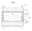
- Fig. 1 is a cross-sectional view schematically showing a dye-sensitized solar cell (cell) according to an embodiment of the present invention.
- First Embodiment Fig. 1 is a cross-sectional view schematically showing one embodiment of a dye-sensitized solar cell (solar cell, cell) according to the present invention.
- the dye-sensitized solar cell 100 has a photoelectric conversion electrode (working electrode) 21; a counter electrode 31 that is arranged apart from the photoelectric conversion electrode 21 so as to face the photoelectric conversion electrode 21; a sealing material 41 that is formed so as to surround the peripheries of the photoelectric conversion electrode 21 and the counter electrode 31; and an electrolyte 51 sealed in a sealed space defined by the photoelectric conversion electrode 21, the counter electrode 31 and the sealing material 41.
- the photoelectric conversion electrode 21 is equipped with a base 12 having a conductive surface 12a, and a short circuit- prevention layer 13 and a dye-supported metal oxide layer 14a are formed on the conductive surface 12a.
- the base 12 having the conductive surface 12a include a conductive base and a base having a transparent conductive film on a part of the base or on the entire base, such as a conductive PET film.
- the type, size and shape of the base 12 are not particularly limited so long as the base 12 can support at least the short circuit-prevention layer 13 and the dye-supported metal oxide layer 14a.
- a plate-like base or a sheet-like base is preferably used.
- the base 12 preferably has a translucency, and more preferably has an excellent translucency with respect to light in the visible range.
- the base 12 preferably has flexibility, and the base 12 having flexibility can provide structures of various shapes by making good use of the flexibility.
- Specific examples of the base 12 include a glass substrate, a plastic substrate such as polyethylene terephthalate, polyethylene, polypropylene, and polystyrene, a metal substrate, an alloy substrate, a ceramic substrate, and a laminate of these substrates.
- the conductive surface 12a of the base 12 may be subjected to various types of known surface modification treatments as needed.
- Specific examples of the surface modification treatment include known surface treatments such as: a degreasing treatment with a surfactant, an organic solvent, an aqueous alkaline solution, or the like; a mechanical polishing treatment; an immersion treatment in an aqueous solution; a preliminary electrolysis treatment with an electrolyte solution; a washing treatment; and a drying treatment.
- the short circuit-prevention layer 13 is patterned in a frame shape.
- the short circuit-prevention layer 13 is formed in a rectangular frame shape, where the outer size and the inner size of the frame shape are substantially similar to the outer size of the dye-supported metal oxide layer 14a, and the width of the frame (the width of the frame member) is ⁇ t.
- the shape (planar shape) of the short circuit-prevention layer 13 is not particularly limited, and any shape can be employed.
- the short circuit-prevention layer 13 is formed in a frame shape in this embodiment in view of an improvement in sealing stability.
- the short circuit-prevention layer 13 is required to have a higher insulation properties as compared to the conductive surface 12a of the base 12.
- the insulation properties of the short circuit-prevention layer 13 is not particularly limited and may be determined in accordance with the conductivity of the electrolyte 51 so as to prevent a short circuit between the electrolyte 51 and the conductive surface 12a of the base 12, it is preferably 2 M ⁇ or higher, more preferably 5 M ⁇ or higher, and even more preferably 10 M ⁇ or higher.
- the insulation properties of the short circuit-prevention layer 13 may be appropriately determined depending on the raw material and the thickness of the film.
- a raw material constituting the short circuit-prevention layer 13 is not particularly limited and may be appropriately selected from known materials. In this embodiment, it is preferable that the raw material constituting the short circuit-prevention layer 13 is difficult to be dissolved in the electrolyte 51 and exhibits an excellent adhesiveness to the sealing material 41.
- Specific examples of the raw materials include: an inorganic oxide such as silicon oxide, aluminum oxide and zirconium oxide; and a resin composition such as UV curable resin, thermosetting resin and thermoplastic resin.
- the resin composition examples include (meth)acrylic-based resin, polyolefin-based resin, urethane-based resin , urethane acrylate-based resin, silicone-based resin, modified silicone-based resin, reactive polyisobutylene resin, epoxy-based resin, epoxy acrylate-based resin, polyether-based resin, polyester-based resin, fluorine-based resin, natural rubber, synthetic rubber and silane coupling agent, but the resin composition is not limited thereto. Note that these resin compositions may be used alone or in combination.
- the raw material constituting the short circuit-prevention layer 13 is preferably an inorganic oxide in consideration of insulation properties and stability in film fabrication.
- the thickness of the short circuit-prevention layer 13 is not particularly limited so long as: it can ensure insulation between the electrolyte 51 and the conductive surface 12a of the base 12; and it is thinner than the dye-supported metal oxide layer 14a, the thickness is preferably from 1 nm to 10 ⁇ m, more preferably from 10 nm to 5 ⁇ m, and even more preferably from 50 nm to 1 ⁇ m. If the thickness of the short circuit-prevention layer 13 is less than 1 nm, it would be difficult to form the film and the film thickness would become nonuniform, which would tend to make it difficult to ensure the insulation. If the thickness of the short circuit-prevention layer 13 exceeds 1 ⁇ m, productivity and cost efficiency would tend to be lowered.
- the thickness of the short circuit-prevention layer 13 is equal to or larger than the thickness of dye-supported metal oxide layer 14a, it would tend to be difficult to uniformly form the dye-supported metal oxide layer 14a and thus difficult to seal the cell, and therefore the thickness of the short circuit-prevention layer 13 is preferably equal to or less than one-tenth of the thickness of the dye-supported metal oxide layer 14a.
- the dye-supported metal oxide layer 14a is formed so as to cover the conductive surface 12a of the base 12. Specifically, the dye-supported metal oxide layer 14a is formed on the conductive surface 12a of the base 12 in the frame of the short circuit-prevention layer 13 and on the frame of the short circuit-prevention layer 13, and thus the dye-supported metal oxide layer 14a is configured to extend onto the short circuit-prevention layer 13.
- the electrolyte 51 sealed in the sealed space defined by the photoelectric conversion electrode 21, the counter electrode 31 and the sealing material 41 is spaced apart from the conductive surface 12a of the base 12, and consequently the electrolyte 51 and the conductive surface 12a of the base 12 are prevented from making contact with each other.
- the dye-supported metal oxide layer 14a has a configuration in which a dye is supported on (adsorbed in) the porous metal oxide layer 14.
- the metal oxide constituting the dye-supported metal oxide layer 14a is not particularly limited, and examples thereof include titanium oxide, zinc oxide, tin oxide, niobium oxide, zirconium oxide, tungsten oxide, silicon oxide, aluminum oxide, and mixtures thereof. Note that these metal oxides may be used alone or in combination.
- the metal oxide may contain: metal such as titanium, tin, zinc, iron, tungsten, zirconium, strontium, indium, cerium, vanadium, niobium, tantalum, cadmium, lead, antimony and bismuth; metal oxides thereof; and metal chalcogenide thereof.
- metal such as titanium, tin, zinc, iron, tungsten, zirconium, strontium, indium, cerium, vanadium, niobium, tantalum, cadmium, lead, antimony and bismuth
- metal oxides thereof metal oxides thereof
- metal chalcogenide thereof metal chalcogenide thereof.
- titanium oxide and zinc oxide are preferable since they can be formed at relatively low cost and have high photoelectric conversion characteristics.
- a dye constituting the dye-supported metal oxide layer 14a is not particularly limited, and may be any of, for example, a water-soluble dye, a non water-soluble dye, or an oil-soluble dye.
- a dye having a desired photo-absorption band and absorption spectrum may be appropriately selected according to the performance required for a photoelectric conversion electrode. By using a sensitive dye, the performance of a photoelectric conversion device can be further enhanced.
- the dye constituting the dye-supported metal oxide layer 14a include a xanthene-based dye such as eosin Y, a coumarin-based dye, a triphenylmethane-based dye, a cyanine-based dye, a merocyanine-based dye, a phthalocyanine-based dye, a porphyrin-based dye, a polypyridine metal complex dye, a ruthenium bipyridinium-based dye, an azo dye, a quinone-based dye, a quinonimine-based dye, a quinacridone-based dye, a squarium-based dye, a perylene-based dye, an indigo-based dye, and a naphthalocyanine-based dye, but the dye is not particularly limited to these examples.
- a xanthene-based dye such as eosin Y, a coumarin-based dye, a triphenylmethane-based dye, a
- the dye preferably has an adsorptive group (e.g., a carboxyl group, a sulfonic group, and a phosphoric group) that interacts with a metal oxide.
- an adsorptive group e.g., a carboxyl group, a sulfonic group, and a phosphoric group
- the thickness of the dye-supported metal oxide layer 14a is not particularly limited, it is preferably from 0.05 to 50 ⁇ m, more preferably from 0.1 to 40 ⁇ m, and even more preferably from 1 to 30 ⁇ m. If this thickness is less than 0.05 ⁇ m, a short circuit-photocurrent (J SC ) might become low since the layer does not support sufficient dye. On the other hand, if the thickness exceeds 50 ⁇ m, the strength of the film might become insufficient or the fill factor (ff) might become low.
- the counter electrode 31 is equipped with a transparent substrate 32 having a conductive substrate 32a.
- the above-described transparent conductive film is formed as the conductive surface 32a on the transparent substrate 32.
- the transparent substrate 32 and the conductive surface 32a correspond respectively to the above-described translucent base 12 and the conductive surface 12a, and the raw materials, types, formation methods for the transparent substrate 32 and the conductive surface 32a are similar to those for the base 12 and the conductive surface 12a.
- the electrode used as the counter electrode 31 is not limited to those having the structure of this embodiment, and known structures may be appropriately used, e.g., a structure in which a film made of: metal such as platinum, gold, silver, copper, aluminum, indium, molybdenum and titanium; a carbon; a conductive polymer; or the like is formed on a base having conductivity such as a metal plate or on a conductive film on a transparent substrate.
- the sealing material 41 is provided between the photoelectric conversion electrode 21 and the counter electrode 31 so as to surround the periphery of the dye-supported metal oxide layer 14a arranged between the photoelectric conversion electrode 21 and the counter electrode 31.
- the sealing material 41 is formed in a substantially rectangular frame shape so as to have an internal size wider than the external size of the dye-supported metal oxide layer 14a and to cover a part of the short circuit-prevention layer 13. With such a configuration, the dye-supported metal oxide layer 14 and the sealing material 41 are spaced apart from each other by a predetermined distance ⁇ s.
- the sealing material 41 may be appropriately used for the raw material (sealant) constituting the sealing material 41 without any particular limitation.
- a UV curable material may be selected when a photo-curing reaction by UV light irradiation is used, while a thermosetting material may be selected when a thermosetting reaction is used.
- the sealing material 41 since the sealing material 41 is prevented from infiltrating into the dye-supported metal oxide layer 14a as described above, the sealing material 41 may preferably be a cured resin article which is obtained by curing an uncured resin composition.
- a resin composition constituting the sealing material 41 include (meth)acrylic-based resin, polyolefin-based resin, urethane-based resin, urethane acrylate-based resin, silicone-based resin, modified silicone-based resin, polyisobutylene resin, polybutadiene resin, epoxy-based resin, epoxy acrylate-based resin, polyether-based resin, polyester-based resin, fluorine-based resin, and mixtures thereof, and these resin compositions may be used, with an addition of a reactive functional group as appropriate, through a thermosetting or photo-curing reaction.
- sealing agent e.g., a resin sheet made of polyethylene, polyethylene fluoride ionomer, or the like may be used as the sealing material 41. Note that they may be used alone or in combination. Among these, the materials which exhibit an excellent adhesiveness with respect to the short circuit-prevention layer 13 are preferably used as the sealing material 41, and more specifically, selecting the same or the same type of raw material as the raw material of the short circuit-prevention layer 13 is preferable.
- a resin composition constituting the sealing material 41 is more preferably a UV curable resin or a thermosetting resin, and even more preferably a UV curable resin.
- the sealing material 41 is used in combination with a solid spacer.
- the use of the solid spacer enables the distance between the photoelectric conversion electrode 21 and the counter electrode 31 to be controlled accurately, enhances the mechanical strength with respect to stress applied from the outside, and improves sealing performance (hermetic performance).
- Specific examples of the solid spacer include a glass bead, various types of resin molded products, silica, woven fabric and non-woven fabric, but the solid spacer is not particularly limited thereto.
- a quasi-solid electrolyte containing conductive particles is used as the electrolyte 51.
- the term “quasi-solid” means the concept which includes not only a solid but also a gel solid or a clayey solid that show almost no fluidity but is deformable by application of stress.
- the term “quasi-solid” means a property of having no shape change or only a slight shape change under its own weight after being left standing for a predetermined time period.
- the conductive particles contained in the electrolyte 51 are preferably conductive carbon materials, specific examples of which include carbon black, carbon fiber, carbon nanotube, graphite, activated carbon, and fullerene. Note that these materials may be used alone or in combination. In consideration of conductivity and economic efficiency, carbon black, carbon fiber, graphite, and carbon nanotube are preferable, and carbon black is more preferable. Specific examples of carbon black include ketjen black, acetylene black, and oil furnace black.
- the average particle diameter of secondary particles of the conductive particles is not particularly limited and may be set such that it can prevent the conductive particles from intruding into a deep part of the dye-supported metal oxide layer 14a, but, in general, the average particle diameter is preferably from the order of nanometers to the order of micrometers.
- the content of the conductive carbon material may be appropriately set according to the required performance and is not particularly limited, but the content in the total quasi-solid electrolyte is preferably from 5 to 80 wt% and more preferably from 20 to 60 wt%.
- the quasi-solid electrolyte preferably contains a redox agent.
- the redox agent is not particularly limited, specific examples of the redox agent include a combination of iodine and iodide (e.g., metal iodide, quarternary ammonium iodide, or the like), a combination of bromine and bromide (e.g., metal bromide, quarternary ammonium bromide, or the like), and a combination of chlorine and a chlorine compound (e.g., metal chloride, quarternary ammonium chloride, or the like).
- iodine-based redox agent tends to provide high photoelectric conversion efficiency.
- the content of the redox agent in the total quasi-solid electrolyte is preferably from 1 ⁇ 10 -4 to 1 ⁇ 10 -2 mol/g, and more preferably from 1 ⁇ 10 -3 to 1 ⁇ 10 -2 mol/g.
- the quasi-solid electrolyte may contain a solvent, so long as the quasi-solid property can be maintained.
- the solvent is not particularly limited, specific examples of the solvent include: nitriles such as acetonitrile, methoxyacetonitrile, propionitrile, 3-methoxypropionitrile, butoxypropionitrile, benzonitrile, and nitrile valerate; carbonates such as dimethyl carbonate, diethyl carbonate, methylethyl carbonate, ethylene carbonate, and propylene carbonate; monohydric alcohols such as ethylene glycol monoalkyl ether, propylene glycol monoalkyl ether, polyethylene glycol monoalkyl ether, and polypropylene glycol monoalkyl ether; polyhydric alcohols such as ethylene glycol, propylene glycol, polyethylene glycol, polypropylene glycol, and glycerin; esters such as ethyl acetate and methyl propionate; ethers such as
- the quasi-solid electrolyte may contain a fire-retardant, low-volatile ionic liquid, so long as the quasi-solid property can be maintained.
- a fire-retardant, low-volatile ionic liquid for example, an imidazolium-based iodine compound such as methylpropyl imidazolium iodide and methylbutyl imidazolium iodide is widely used as the ionic liquid.
- the ionic liquid is not particularly limited to those mentioned above, and a known ionic liquid may be used.
- the ionic liquid examples include an ionic liquid such as imidazolium-based, pyridine-based, alicyclic amine-based, aliphatic amine-based, and azonium amine-based, and an ionic liquid described in European Patent No. 718288 , WO 95/18456 Pamphlet, J. Electrochem. Soc. Vol. 143, No.10, p.3099 (1996 ), and Inorg. Chem. Vo1.35, p.1168 (1996 ). Note that they may be used alone or in combination.
- the content of the ionic liquid in the total quasi-solid electrolyte is preferably 1 to 80 wt%.
- the quasi-solid electrolyte may contain particles.
- the particles include TiO 2 , SnO 2 , SiO 2 , ZnO, Nb 2 O 5 , In 2 O 3 , ZrO 2 , Al 2 O 3 , WO 3 , SrTiO 3 , Ta 2 O 5 , La 2 O 3 , Y 2 O 3 , Ho 2 O 3 , Bi 2 O 3 , CeO 2 , and C. Note that they may be used alone or in combination.
- the average particle diameter of the particles is not particularly limited, but is preferably about 2 to 1000 nm.
- the quasi-solid electrolyte may contain various additives according to required performance.
- Additives typically used in batteries, solar cells, and the like can be appropriately used.
- Specific examples of the additives include: a p-type conductive polymer such as polyaniline, polyacetylene, polypyrrole, polythiophene, polyphenylene, polyphenylene vinylene, and a derivative of any of them; a molten salt composed of a combination of a halide ion and an imidazolium ion, a pyridinium ion, a triazolium ion, or a derivative of any of them; a gellant; an oil gellant; a dispersant; a surfactant; and a stabilizer.
- a p-type conductive polymer such as polyaniline, polyacetylene, polypyrrole, polythiophene, polyphenylene, polyphenylene vinylene, and a derivative of any of them
- Preparation of the quasi-solid electrolyte may be performed according to an ordinary method. For example, by mixing or kneading the conductive carbon material with small amounts of solvent, ionic liquid, redox agent, and various types of additives that are added as needed, it is possible to prepare a uniform quasi-solid electrolyte.
- Fig. 2 is a flowchart showing the manufacturing methods of the photoelectric conversion electrode 21 and the dye-sensitized solar cell 100 according to this embodiment.
- the base 12 having the conductive surface 12a is prepared (S1)
- the short circuit-prevention layer 13 is patterned to have a frame shape on the conductive surface 12a (S2)
- the metal oxide layer 14 is formed on the conductive surface 12a in the frame of the short circuit-prevention layer 13 and on the frame of the short circuit-prevention layer 13 (S3)
- the dye-supported metal oxide layer 14a is formed by causing the dye to be supported on (adsorbed in) the metal oxide layer 14 (S4), thereby fabricating the photoelectric conversion electrode 21, being the working electrode.
- the counter electrode 31 is prepared (S5), the electrolyte 51 is arranged between the conductive surface 32a of the counter electrode 31 and the dye-supported metal oxide layer 14a of the photoelectric conversion electrode 21 (S6), and the photoelectric conversion electrode 21 and the counter electrode 31 are bonded to each other via the electrolyte 51 and the peripheries of the photoelectric conversion electrode 21 and the counter electrode 31 are jointed and sealed using a spacer or the like as appropriate (S7), thereby fabricating the dye-sensitized solar cell 100.
- Fig. 3 is a perspective view schematically showing the manufacturing method of the photoelectric conversion electrode 21 according to this embodiment.
- the method of patterning the short circuit-prevention layer 13 on the conductive surface 12a of the base 12 is not particularly limited, and known thin-film formation methods may be applied thereto. Specifically, for example, by applying the above-mentioned insulating material into a frame shape on the conductive surface 12a of the base 12 using a mask, the short circuit-prevention layer 13 can be formed.
- the method of applying the insulating material may be appropriately selected from known techniques including, for example, vacuum deposition, reactive deposition, sputtering, ion plating, vapor deposition such as CVD and PVD, coating techniques such as spray coating, spin coating, dip coating, calendar coating and dispenser coating, transfer process, screen printing, ink jet, sol-gel process, and the like.
- known techniques including, for example, vacuum deposition, reactive deposition, sputtering, ion plating, vapor deposition such as CVD and PVD, coating techniques such as spray coating, spin coating, dip coating, calendar coating and dispenser coating, transfer process, screen printing, ink jet, sol-gel process, and the like.
- coating techniques such as spray coating, spin coating, dip coating, calendar coating and dispenser coating, transfer process, screen printing, ink jet, sol-gel process, and the like.
- various types of known treatment may be provided as needed, examples of which include corona discharge treatment, plasma irradiation treatment, UV light or IR light irradiation treatment,
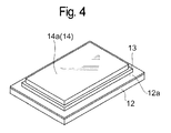
- Fig. 4 is a perspective view schematically showing the manufacturing method of the photoelectric conversion electrode 21 according to this embodiment.
- the method of forming the dye-supported metal oxide layer 14a is not particularly limited, and known formation methods may be applied thereto.
- Examples of the methods include: a method in which a solution (dispersion, suspension) containing the above-described metal oxide is applied onto the conductive surface 12a in the frame of the short circuit-prevention layer 13 and onto the frame of the short circuit-prevention layer 13, and then sintering is performed, or low-temperature treatment at a temperature around 150°C is performed, to form the metal oxide layer (semiconductor layer) 14, and the above-described dye is made to be supported on (adsorbed in) the metal oxide layer 14; and a method in which the metal oxide layer 14 is formed on the conductive surface 12a in the frame of the short circuit-prevention layer 13 and on the frame of the short circuit-prevention layer 13 by vacuum deposition, reactive deposition, sputtering, ion plating, vapor deposition such as CVD and PVD, sol-gel process, or the like, and the above-described dye is made to be supported on (adsorbed in) the metal oxide layer 14.
- electrochemical methods using electrolyte solutions may be employed, examples of which include: a method in which the metal oxide layer 14 may be fabricated on the conductive surface 12a in the frame of the short circuit-prevention layer 13 and on the frame of the short circuit-prevention layer 13 by cathode electrolytic deposition using an electrolyte solution containing the above-described metal oxide and then the above-described dye is made to be supported on (adsorbed in) the metal oxide layer 14; and a method in which cathode electrolytic deposition is performed using an electrolyte solution containing the above-described metal oxide and dye.
- the formation of the metal oxide layer 14 and the causing the dye to be supported can be simultaneously performed to thereby enable the dye-supported metal oxide layer 14a to be promptly formed.
- An electrolysis condition can be appropriately set based on characteristics of the materials to be used, according to an ordinary method. For example, when forming the dye-supported metal oxide layer 14a made of ZnO and the dye, it is preferable for a reduction electrolysis potential to be about from - 0.8 to -1.2 V (vs.
- a bath temperature of the electrolyte solution to be about from 0 to 100°C.
- a metal ion concentration in the electrolyte solution it is preferable for a metal ion concentration in the electrolyte solution to be about from 0.5 to 100 mM, and a dye concentration in the electrolyte solution to be about from 50 to 500 ⁇ M.
- the dye supported on the dye-supported metal oxide layer 14a may be desorbed and another dye may be re-adsorbed thereto.
- the method of causing the dye to be supported on (adsorbed in) the metal oxide layer 14 is not particularly limited and known formation methods may be applied thereto. Examples of the method include a method of immersing the metal oxide layer 14 in a solution containing the dye and a method of coating the metal oxide layer 14 with a solution containing the dye.
- a solvent for the dye-containing solution used here can be appropriately selected from known solvents such as water, an ethanol-based solvent, a nitrile-based solvent, and a ketone-based solvent, according to solubility, compatibility, or the like of the dye to be used.
- step S6 for arranging the electrolyte 51 the method of arranging the quasi-solid electrolyte is not particularly limited, and known formation methods may be applied thereto.
- the methods include: a method the quasi-solid electrolyte is directly coated onto the dye-supported metal oxide layer 14a and then pressed; and a method in which the quasi-solid electrolyte is diluted with a solvent, the resulting quasi-solid electrolyte having a low viscosity is directly coated onto the dye-supported metal oxide layer 14a, and then the solvent is removed; however, the methods are not limited to these examples.
- the timing at which the electrolyte 51 is sealed is not particularly limited to the above example.
- the electrolyte 51 may be injected into the sealed space from an inlet port (not shown) that is formed separately, and then the inlet port may be sealed.
- the dye-sensitized solar cell 100 In the dye-sensitized solar cell 100 according to this embodiment, a short circuit between the conductive surface 12a of the base 12 and the electrolyte 51 is prevented by the short circuit-prevention layer 13 and the dye-supported metal oxide layer 14a in the region where the dye-supported metal oxide layer 14a is not formed, while such a short circuit is prevented by the dye-supported metal oxide layer 14a not allowing the intrusion of the conductive particles of the electrolyte 51 in the region where the dye-supported metal oxide layer 14a is formed.
- the dye-sensitized solar cell 100 is advantageous as compared to the related art with respect to the point that the short circuit within the cell can be securely prevented even when a highly-conductive electrolyte 51 is used.
- the dye-supported metal oxide layer 14a is formed, not via the short circuit-prevention layer 13, but directly on the conductive surface 12a of the base 12, the cell resistance is not increased unintentionally.
- the dye-supported metal oxide layer 14a and the sealing material 41 are arranged apart from each other via the short circuit-prevention layer 13, and the sealing material 41 is thereby prevented from infiltrating into the dye-supported metal oxide layer 14a, which suppresses degradation of the photoelectric conversion characteristics and the durability that might be caused by such infiltration of the sealing material 41. Accordingly, the dye-sensitized solar cell 100 in this embodiment provides improved photoelectric conversion characteristics as well as improved durability as compared to the related art, and therefore provides improved reliability.
- the dye-sensitized solar cell 100 having excellent photoelectric conversion characteristics can be manufactured easily, stably, and at a low cost, without unintentionally increasing the cell resistance and unintentionally degrading the photoelectric conversion characteristics and the durability. Accordingly, the resulting dye-sensitized solar cell 100 achieves enhanced productivity and enhanced economic efficiency.
- the dye-supported metal oxide layer 14a may be formed so as to cover only the conductive surface 12a in the frame of the short circuit-prevention layer 13.
- the configuration in which the dye-supported metal oxide layer 14a covers a part of the short circuit-prevention layer 13 may be omitted.
- the configuration in which the sealing material 41 covers a part of the short circuit-prevention layer 13 may be omitted.
- the conductive surface 12a may be formed only on a part of the base 12, and the short circuit-prevention layer 13 may be formed on the base 12 and the conductive surface 12a and/or on the base 12.
- Example 1 First, a transparent glass substrate (TCO: manufactured by AGC Fabritech CO., LTD. (size: 25 mm long x 25 mm wide)) having a transparent conductive film made of SnO 2 doped with fluorine was prepared as a base and was pre-rinsed.
- TCO transparent glass substrate
- AGC Fabritech CO., LTD. size: 25 mm long x 25 mm wide
- a film of silica was formed so as to have the thickness of about 300 nm by sputtering, and by removing the kapton tape from the transparent glass substrate, a short circuit-prevention layer having a frame shape (external size: 10.0 mm long x 10.0 mm wide, internal size: 5.0 mm long x 5.0 mm wide, frame width ⁇ t: 2.5 mm) was patterned.
- zinc oxide particles (trade name "nano ZINC100,” manufactured by Honjo Chemical Corporation) were added to toluene in an amount of 30 wt%, and a dispersion process was carried out for 30 minutes using a paint shaker to obtain a zinc oxide slurry.
- This zinc oxide slurry was coated onto the transparent conductive film, positioned in the frame of the short circuit-prevention layer, of the transparent glass substrate and onto the short circuit-prevention layer, and was then dried by heating at 100 °C for 30 minutes using an electric furnace. The rate of temperature increase was 2 °C/min. The coating of the zinc oxide slurry and the heating were repeated five times.
- a metal oxide layer (zinc oxide layer) having a rectangular shape in plan view (7.0 mm long x 7.0 mm wide x 10 ⁇ m thick) was formed so as to completely cover the transparent conductive film in the frame of the short circuit-prevention layer and to extend onto the short circuit-prevention layer by about 1.0 mm.
- a solution of CH 3 CN containing 500 ⁇ M of dye represented by the formula below was prepared as a dye-containing solution.
- the metal oxide layer which had been subjected to cathode electrolytic deposition, and then rinsed with purified water and dried, was immersed, so that the dye was adsorbed into the metal oxide layer. Then the metal oxide layer was rinsed with acetonitrile solution and dried to form a dye-supported metal oxide layer.
- a photoelectric conversion electrode of Example 1 which has a structure similar to those shown in Figs. 1 and 4 , was fabricated.
- a quasi-solid electrolyte obtained by mixing and kneading carbon black, tetrabutylammonium iodide and 3-methoxypropionitrile was coated onto the dye-supported metal oxide layer so as to cover it.
- a UV curable adhesive (31 x 101C manufactured by ThreeBond, Co., Ltd.) was coated in a frame shape onto the substrate of the photoelectric conversion electrode using a dispenser.
- the UV curable adhesive was coated to have a width of about 1.0 mm from the outer end of the substrate of the photoelectric conversion electrode so as to be spaced apart from the dye-supported metal oxide layer.
- the counter electrode was bonded to the photoelectric conversion electrode via the quasi-solid electrolyte and the spacer, and then the UV curable adhesive was cured by irradiating it with UV light, thereby providing sealing.
- the cured UV curable adhesive had a width of about 1.5 mm, and while the cured UV curable adhesive was spaced apart from the dye-supported metal oxide layer, a part thereof extended onto the short circuit-prevention layer from the substrate of the photoelectric conversion electrode.
- Comparative Example 1 A photoelectric conversion electrode of Comparative Example 1 was fabricated with the same operations as those in Example 1, except that the formation of the short circuit-prevention layer was omitted and a metal oxide layer having a rectangular shape in plan view (7.0 mm long x 7.0 mm wide x 10 ⁇ m thick) was formed using a mask. Using the resulting photoelectric conversion electrode of Comparative Example 1, a dye-sensitized solar cell of Comparative Example 1 was fabricated with the same operations as those in Example 1, except that a UV-curable resin was coated in a frame shape having a width of about 1.0 mm so as to make close contact with the periphery of the dye-supported metal oxide layer.
- Comparative Example 2 A photoelectric conversion electrode of Comparative Example 2 was fabricated with the same operations as those in Example 1, except that, after a metal oxide layer having a rectangular shape in plan view (7.0 mm long x 7.0 mm wide x 10 ⁇ m thick) was formed using a mask, this metal oxide layer was immersed in an ethanol solution of aluminum butoxide and then dried, thereby forming an aluminum oxide film on a surface of the transparent conductive film that was not covered with the metal oxide layer, and then the dye is made to be supported on the metal oxide layer.
- a dye-sensitized solar cell of Comparative Example 2 was fabricated with the same operations as those in Example 1, except that a UV-curable resin was coated in a frame shape having a width of about 1.0 mm from the outer end of the substrate of the photoelectric conversion electrode so as to be spaced apart from the dye-supported metal oxide layer.
- Comparative Example 3 A photoelectric conversion electrode of Comparative Example 3 was fabricated with the same operations as those in Example 1, except that the formation of the short circuit-prevention layer was omitted and a metal oxide layer having a rectangular shape in plan view (7.0 mm long x 7.0 mm wide x 10 ⁇ m thick) was formed using a mask.
- a dye-sensitized solar cell of Comparative Example 3 was fabricated with the same operations as those in Example 1, except that a UV-curable resin was coated in a frame shape having a width of about 1.0 mm from the outer end of the substrate of the photoelectric conversion electrode so as to be spaced apart from the dye-supported metal oxide layer.
- the resulting dye-sensitized solar cell of Comparative Example 3 had a structure in which the electrolyte and the transparent conductive film of the substrate are in contact with each other.
- the photoelectric conversion efficiency ( ⁇ : %) of each of the dye-sensitized solar cells (cells) of Example 1 and Comparative Examples 1 to 3 was measured using a solar simulator of AM-1.5 (1000W/m 2 ). Note that the photoelectric conversion efficiency ( ⁇ : %) is expressed as a percentage obtained by: dividing the maximum output, which is a product of a voltage and a current obtained by sweeping the voltage of a photoelectric conversion device using a source meter and measuring a response current, by a light intensity per 1 cm 2 ; and multiplying the resulting value by 100.
- Fig. 5 shows the evaluation results of the dye-sensitized solar cells (cells) of the Example and Comparative Examples 1 and 2. Note that Comparative Example 3 could not function as a dye-sensitized solar cell since the transparent conductive film of the substrate and the quasi-solid electrolyte made contact with each other and a short circuit occurred, and therefore the evaluation result of Comparative Example 3 was omitted in Fig. 5 .
- the dye-sensitized solar cell of Example 1 was verified to provide superior photo-conversion characteristics and durability as compared to those in the dye-sensitized solar cell of Comparison Example 1 for which the formation of the short circuit-prevention layer was omitted.
- This result suggested that, in the case where the dye-supported metal oxide electrode and the UV-curable resin are in close contact with each other as in Comparative Example 1, an uncured UV-curable resin intruded into the pores of the dye-supported metal oxide electrode, which degraded the photoelectric conversion characteristics and the durability.
- the dye-sensitized solar cell of Example 1 was verified to provide superior photo-conversion characteristics and durability as compared to those in the dye-sensitized solar cell of Comparison Example 2 in which the short circuit-prevention layer made of aluminum oxide was formed after the formation of the metal oxide electrode as in the related art.
- the dye-sensitized solar cell of Comparative Example 2 exhibited lower current and voltage, which suggests that the performance of the device itself was degraded.
- the dye-sensitized solar cell, the manufacturing method thereof, and the manufacturing method of the working electrode for the dye-sensitized solar cell in the present invention can prevent, even when a highly-conductive electrolyte is employed, a short circuit between a transparent conductive film of the working electrode and the electrolyte, and can enhance the reliability with improved photoelectric conversion characteristics and improved durability. Accordingly, the present invention can be widely applied to electronic or electric devices including the dye-sensitized solar cell, as well as various types of appliances, equipment, systems and the like that include these electronic and electric devices.
Landscapes
- Engineering & Computer Science (AREA)
- Power Engineering (AREA)
- Microelectronics & Electronic Packaging (AREA)
- Chemical & Material Sciences (AREA)
- Chemical Kinetics & Catalysis (AREA)
- Electrochemistry (AREA)
- Photovoltaic Devices (AREA)
- Hybrid Cells (AREA)
Abstract
It is an object of the present invention to provide a dye-sensitized solar cell, etc. capable of preventing, even when a highly-conductive electrolyte is employed, a short circuit between a transparent conductive film of a working electrode and the electrolyte, and thereby enhancing reliability with improved photoelectric conversion characteristics and improved durability.
A short circuit-prevention layer is patterned in a frame shape so as to surround the periphery of a dye-supported metal oxide layer on a region of a conductive surface where the dye-supported metal oxide layer is not formed. The short circuit-prevention layer is formed to be thinner than the dye-supported metal oxide layer, and the dye-supported metal oxide layer is formed so as to cover the conductive surface in the frame of the short circuit-prevention layer and to extend onto the short circuit-prevention layer. The dye-supported metal oxide layer and a sealing material are arranged apart from each other via the short circuit-prevention layer.
Description
- This application relates to and claims priority from Japanese Patent Application No.
2009-227302, filed on September 30, 2009 - The present invention relates to a dye-sensitized solar cell, a manufacturing method of the same, and a manufacturing method of a working electrode for the dye-sensitized solar cell.
- In recent years, dye-sensitized solar cells have gained increasing interest, since the dye-sensitized solar cells can be manufactured at low cost and have a higher photoelectric conversion efficiency among organic solar cells. A dye-sensitized solar cell has three primary elements - a working electrode, an electrolyte and a counter electrode. A working electrode which is typically used is configured in such a way that a porous dye-supported metal oxide layer is formed on a transparent conductive film formed on a substrate. A typical dye-supported metal oxide layer is configured in such a way that a sensitizing dye is supported on (adsorbed in) a metal oxide semiconductor (metal oxide layer). A known counter electrode is configured in such a way that a platinum film is formed on a transparent conductive film formed on a substrate. In order to manufacture dye-sensitized solar cells (cells) of this type, generally, a working electrode and a counter electrode are arranged apart from each other so as to face each other, where a sealing material is provided at the outer ends of the facing surfaces of these electrodes to seal and joint the peripheries of the electrodes, and an electrolyte is sealed in a space defined by such sealing.
- Of the electrolytes used for the dye-sensitized solar cells, a liquid type electrolyte (electrolyte solution) containing organic solvent is widely known. However, the use of such an electrolyte solution might cause the leakage of the solution, fire and explosion associated with such leakage, environmental contamination resulting from the volatilization of solvent, etc. Accordingly, it has been an important object in recent years to achieve quasi-solid (solidified, gelled, etc.) electrolytes.
- As an example of such quasi-solid electrolytes, a quasi-solid electrolyte obtained by mixing and kneading a highly-conductive carbon material such as carbon black and a trace amount of solvent into a paste is known. Such a quasi-solid electrolyte can achieve a high photoelectric conversion efficiency even without the use of a platinum catalyst in the counter electrode, and is thus considered as constituting one important element for achieving the improvement of photoelectric conversion efficiency, as well as achieving cost reduction, of dye-sensitized solar cells.
- However, since the carbon material in the quasi-solid electrolyte above has a very high conductivity, a short circuit occurs between the transparent conductive film of the working electrode and the counter electrode when the quasi-solid electrolyte makes contact with, even if only slightly, the transparent conductive film below the metal oxide semiconductor, which results in the problem that the photoelectric conversion characteristics of the resulting dye-sensitized solar cell are degraded. In other words, the highly-conductive electrolyte makes it more difficult to seal the solar cell (cell) as compared to the liquid-type electrolyte, and therefore there has been a desire to develop highly-reliable cell shapes that enable sealing without causing a short circuit during cell fabrication even when a highly-conductive electrolyte is used.
- As a technique for preventing a short circuit in dye-sensitized solar cells, for example, Japanese laid-open publication No.
2005-108807 2008-059851 2004-087622 Patent Documents 2 and 3). - Patent Document 1: Japanese laid-open publication No.
2005-108807 - Patent Document 2: Japanese laid-open publication No.
2008-059851 - Patent document 3: Japanese laid-open publication No.
2004-087622 - However, in the technique of
Patent Invention 1, since the short circuit-prevention layer that is a thin but dense layer with a small resistivity using a material, such as N-type conductive polymer or a fullerene having a small resistivity and dense film texture, the short circuit-prevention layer does not provide sufficient insulation, and thus, in the configuration where a highly-conductive electrolyte (e.g., the above-mentioned quasi-solid electrolyte) is employed, a short circuit might occur between the transparent conductive film and the electrolyte. On the other hand, since the short circuit-prevention layer, even though its resistivity is small, is formed between the dye-supported metal oxide layer and the transparent conductive film, the short circuit-prevention layer performs as an internal resistance and increases the cell resistance, which might degrade the photoelectric conversion characteristics. In addition, the substances such as N-type conductive polymer and fullerene absorb light in the visible range, and thus might reduce the amount of light incident on the working electrode, thereby degrading the photoelectric conversion characteristics. - On the other hand, in the techniques in
Patent Documents 2 and 3, since the short circuit-prevention layer is formed on the metal oxide layer, it is substantially impossible to completely cover only the region of the transparent conductive film which is not provided with the metal oxide layer with the short circuit-prevention layer, and therefore these techniques are not sufficiently reliable in preventing a short circuit between the transparent conductive film and the electrolyte. In order to avoid such a problem, the short circuit-prevention layer must be formed also on the metal oxide layer; however, such a configuration would reduce the surface area of the metal oxide layer, and thus cause degradation of the photoelectric conversion characteristics. - Another possible solution would be a configuration in which, in order to avoid contact between the transparent conductive film of the working electrode and the electrolyte, the inner peripheral wall of the sealing material for sealing the cell and the outer peripheral wall of the dye-supported metal oxide layer are formed in close contact without any gap therebetween, so that a region in the transparent conductive film which is exposed without the dye-supported metal oxide layer formed thereon does not exist in the cell in which the electrolyte is sealed. However, with such a configuration, resin that is left uncured when the sealing material is cured would infiltrate into the porous metal oxide layer, which would cause the photoelectric conversion characteristics to be degraded, and furthermore, would decrease the durability of the dye-sensitized solar cell because the resin would be cured or deteriorated in the dye-supported metal oxide layer during a long period of use and/or the presence of the resin would cause the electrolyte and dye to be deteriorated or decomposed.
- The present invention has been made in view of the circumstances above, and it is an object of the present invention to provide a dye-sensitized solar cell that are capable of preventing, even when a highly-conductive electrolyte is employed, a short circuit between a transparent conductive layer of the working electrode and the electrolyte and thus providing high reliability with improved photoelectric conversion characteristics and improved durability, a manufacturing method thereof, and a manufacturing method of a working electrode for the dye-sensitized solar cell.
- In order to achieve the object above, the inventors of the present invention have committed to intensive research and found that the problem above can be solved by re-designing the shape of a cell and configuring a conductive surface of a working electrode, a dye-supported metal oxide layer and a sealing material in predetermined shapes, thereby achieving the present invention.
- A dye-sensitized solar cell according to an aspect of the present invention includes: a working electrode; a counter electrode that is arranged apart from the working electrode so as to face the working electrode; an electrolyte provided between the working electrode and the counter electrode; and a sealing material that seals the electrolyte, wherein: the electrolyte is a quasi-solid electrolyte comprising conductive particles; the working electrode has a base having a conductive surface and a dye-supported metal oxide layer formed on a part of the conductive surface; a short circuit-prevention layer is patterned in a frame shape in a region on the conductive surface where the dye-supported metal oxide layer is not formed, so as to surround a periphery of the dye-supported metal oxide layer; the short circuit-prevention layer is formed to be thinner than the dye-supported metal oxide layer, and the dye-supported metal oxide layer is formed so as to cover the conductive surface in the frame of the short circuit-prevention layer and to extend onto the short circuit-prevention layer; and the dye-supported metal oxide layer and the sealing material are arranged apart from each other via the short circuit-prevention layer.
- The "frame shape" in this specification refers to a shape that surrounds the periphery of the dye-supported metal oxide layer, and to the concept which includes, for example, a triangle, a rectangle, a polygon, a star shape, a geometric shape, a circle, an ellipse, an indefinite shape, and a shape formed by connecting these shapes together.
- When the inventors measured the characteristics of the dye-sensitized solar cell configured as described above, they found out that the photoelectric conversion characteristics and durability have been remarkably improved as compared to the related art. Although the details of the functional mechanism that contributes to such effects are still unclear, for example the following presumption can be made.
- In the dye-sensitized solar cell having the configuration above, the short circuit-prevention layer is formed in a frame shape on the region of the conductive surface where the dye-supported metal oxide layer is not formed, so as to surround the periphery of the dye-supported metal oxide layer, and the dye-supported metal oxide layer is formed so as to cover the conductive surface of the working electrode in the frame of the short circuit-prevention layer and to extend onto the short circuit-prevention layer, and therefore a short circuit is prevented both in the region where the dye-supported metal oxide layer is formed and in the region where the dye-supported metal oxide layer is not formed.
Specifically, in the region where the dye-supported metal oxide layer is not formed, since the electrolyte and the conductive surface of the working electrode are structurally spaced apart from each other by the short circuit-prevention layer and the dye-supported metal oxide layer projected from the inner side of the frame of the short circuit-prevention layer onto the short circuit-prevention layer, contact between the electrolyte and the conductive surface of the working electrode is blocked by the dye-supported metal oxide layer and the short circuit-prevention layer, thereby ensuring that a short circuit is prevented.
On the other hand, in the region where the dye-supported metal oxide layer is formed, since the dye-supported metal oxide layer does not allow the quasi-solid electrolyte to infiltrate into a deep part thereof, contact between the electrolyte and the conductive surface of the working electrode, which could occur due to the infiltration of a liquid-type electrolyte into dye-supported metal oxide layer in the related art, in the region where the dye-supported metal oxide layer is formed is structurally blocked, thereby ensuring that a short circuit is prevented. - Moreover, in the dye-sensitized solar cell having the configuration above, the dye-supported metal oxide layer is formed not via the short circuit-prevention layer but directly on the conductive surface, an increase in cell resistance, which was caused by the short circuit-prevention layer in the related art, can be suppressed.
- Furthermore, in the dye-sensitized solar cell having the configuration above, the dye-supported metal oxide layer and the sealing material are arranged apart from each other via the short circuit-prevention layer, and the sealing material is prevented from being infiltrated into the dye-supported metal oxide layer, and therefore a degradation of the photoelectric conversion characteristics and a decrease in the durability caused by the infiltration of the sealing material can be suppressed.
- As a result of the combination of the effects above, in the dye-sensitized solar cell having the configuration above, it can be inferred that: even when a highly-conductive electrolyte is employed, a short circuit between the transparent conductive film of the working electrode and the electrolyte can be prevented; an increase in cell resistance is suppressed; and the photoelectric conversion characteristics and the durability are remarkably improved. However, effects provided by the present invention are not limited to these effects.
- In the configuration above, it is preferable that the short circuit-prevention layer is not formed on a surface of the dye-supported metal oxide layer. With such a configuration, the surface area of the dye-supported metal oxide layer serving as a light-receiving part will not be reduced, and thus a degradation in the photoelectric conversion characteristics can be suppressed.
- In the configuration above, it is preferable that the sealing material is a cured resin article. Since the sealing material is prevented from being infiltrated into the dye-supported metal oxide layer as described above in the dye-sensitized solar cell having the configuration above, such a configuration may be particularly effective in an embodiment in which an uncured resin composition is cured to form the sealing material.
- A manufacturing method of a working electrode for a dye-sensitized solar cell according to another aspect of the present invention is a method that can effectively fabricate the working electrode for the dye-sensitized solar cell according to the above aspect of the present invention, the method including the steps of: preparing a base having a conductive surface; patterning a short circuit-prevention layer in a frame shape on the conductive surface; and forming a dye-supported metal oxide layer on the conductive surface in the frame of the short circuit-prevention layer and on the frame of the short circuit-prevention layer, the steps being carried out in the this order.
- A manufacturing method of a dye-sensitized solar cell according to another aspect of the invention is a method that can fabricate the dye-sensitized solar cell according to the above aspect of the present invention, the method including the steps of: preparing a base having a conductive surface; patterning a short circuit-prevention layer in a frame shape on the conductive surface; and forming a dye-supported metal oxide layer on the conductive surface in the frame of the short circuit-prevention layer and on the frame of the short circuit-prevention layer and thereby fabricating a working electrode, the steps being carried out in this order, and the method further comprising the steps of: preparing a counter electrode; arranging an electrolyte between the working electrode and the counter electrode; arranging a sealing material on outer ends of opposing surfaces of the working electrode and the counter electrode to seal and joint peripheries of the working electrode and the counter electrode, the sealing material being arranged apart from the dye-supported metal oxide layer.
- In the manufacturing methods above, for the same reasons, it is preferable that the short circuit-prevention layer is not formed on a surface of the dye-supported metal oxide layer. Also, it is preferable that the sealing material is a cured resin article.
- According to the present invention, even when a highly-conductive electrolyte is employed, a short circuit between the transparent conductive film of the working electrode and the electrolyte can be prevented, thereby achieving a dye-sensitized solar cell and a manufacturing method thereof that are highly reliable with improved photoelectric conversion characteristics and improved durability, as well as a manufacturing method of a working electrode that can achieve the dye-sensitized solar cell exhibiting such high performance.
-
Fig. 1 is a cross-sectional view schematically showing a dye-sensitized solar cell (cell) according to an embodiment of the present invention. -
Fig. 2 is a flowchart showing a manufacturing method of a working electrode (photoelectric conversion electrode) and the dye-sensitized solar cell (cell) according to an embodiment of the present invention. -
Fig. 3 is a perspective view schematically showing the manufacturing method of the working electrode (photoelectric conversion electrode) according to an embodiment of the present invention. -
Fig. 4 is a perspective view schematically showing the manufacturing method of the working electrode (photoelectric conversion electrode) according to an embodiment of the present invention. -
Fig. 5 is a graph showing the photoelectric conversion characteristics of dye-sensitized solar cells (cells) in Example 1 and in Comparative Examples 1 and 2. - Embodiments of the present invention will be described below. Note that the same element is denoted with the same reference numerals, and repeated descriptions thereof will be omitted. Also, note that the positional relationships such as top and bottom, as well as right and left, are based on the positional relationships shown in the drawings, unless otherwise particularly specified. Moreover, the ratios of dimensions in the drawings are not limited to the ratios shown. The following embodiments are merely an example for describing the present invention, and the present invention is not limited only to the embodiments.
- First Embodiment
Fig. 1 is a cross-sectional view schematically showing one embodiment of a dye-sensitized solar cell (solar cell, cell) according to the present invention. The dye-sensitizedsolar cell 100 has a photoelectric conversion electrode (working electrode) 21; acounter electrode 31 that is arranged apart from thephotoelectric conversion electrode 21 so as to face thephotoelectric conversion electrode 21; a sealingmaterial 41 that is formed so as to surround the peripheries of thephotoelectric conversion electrode 21 and thecounter electrode 31; and anelectrolyte 51 sealed in a sealed space defined by thephotoelectric conversion electrode 21, thecounter electrode 31 and the sealingmaterial 41. Thephotoelectric conversion electrode 21 is equipped with a base 12 having aconductive surface 12a, and a short circuit-prevention layer 13 and a dye-supportedmetal oxide layer 14a are formed on theconductive surface 12a. - Specific examples of the base 12 having the
conductive surface 12a include a conductive base and a base having a transparent conductive film on a part of the base or on the entire base, such as a conductive PET film. - The type, size and shape of the base 12 are not particularly limited so long as the base 12 can support at least the short circuit-
prevention layer 13 and the dye-supportedmetal oxide layer 14a. For example, a plate-like base or a sheet-like base is preferably used. The base 12 preferably has a translucency, and more preferably has an excellent translucency with respect to light in the visible range. The base 12 preferably has flexibility, and the base 12 having flexibility can provide structures of various shapes by making good use of the flexibility. Specific examples of the base 12 include a glass substrate, a plastic substrate such as polyethylene terephthalate, polyethylene, polypropylene, and polystyrene, a metal substrate, an alloy substrate, a ceramic substrate, and a laminate of these substrates. - Specific examples of a transparent conductive film that may serve as the
conductive surface 12a include ITO, SnO2 InO3 and FTO obtained by doping SnO2 with fluorine. Formation methods for these transparent conductive films are not particularly limited, and known techniques such as deposition, CVD, spraying, spin coating, and dipping can be used. The film thickness of the transparent conductive film can be set appropriately. - The
conductive surface 12a of the base 12 may be subjected to various types of known surface modification treatments as needed. Specific examples of the surface modification treatment include known surface treatments such as: a degreasing treatment with a surfactant, an organic solvent, an aqueous alkaline solution, or the like; a mechanical polishing treatment; an immersion treatment in an aqueous solution; a preliminary electrolysis treatment with an electrolyte solution; a washing treatment; and a drying treatment. - On the
conductive surface 12a of thebase 12, the short circuit-prevention layer 13 is patterned in a frame shape. In this embodiment, the short circuit-prevention layer 13 is formed in a rectangular frame shape, where the outer size and the inner size of the frame shape are substantially similar to the outer size of the dye-supportedmetal oxide layer 14a, and the width of the frame (the width of the frame member) is Δt. Note that the shape (planar shape) of the short circuit-prevention layer 13 is not particularly limited, and any shape can be employed. However, the short circuit-prevention layer 13 is formed in a frame shape in this embodiment in view of an improvement in sealing stability. - The short circuit-
prevention layer 13 is required to have a higher insulation properties as compared to theconductive surface 12a of thebase 12. Although the insulation properties of the short circuit-prevention layer 13 is not particularly limited and may be determined in accordance with the conductivity of theelectrolyte 51 so as to prevent a short circuit between theelectrolyte 51 and theconductive surface 12a of thebase 12, it is preferably 2 MΩ or higher, more preferably 5 MΩ or higher, and even more preferably 10 MΩ or higher. The insulation properties of the short circuit-prevention layer 13 may be appropriately determined depending on the raw material and the thickness of the film. - A raw material constituting the short circuit-prevention layer 13 (insulating material) is not particularly limited and may be appropriately selected from known materials. In this embodiment, it is preferable that the raw material constituting the short circuit-
prevention layer 13 is difficult to be dissolved in theelectrolyte 51 and exhibits an excellent adhesiveness to the sealingmaterial 41. Specific examples of the raw materials include: an inorganic oxide such as silicon oxide, aluminum oxide and zirconium oxide; and a resin composition such as UV curable resin, thermosetting resin and thermoplastic resin. Specific examples of the resin composition include (meth)acrylic-based resin, polyolefin-based resin, urethane-based resin , urethane acrylate-based resin, silicone-based resin, modified silicone-based resin, reactive polyisobutylene resin, epoxy-based resin, epoxy acrylate-based resin, polyether-based resin, polyester-based resin, fluorine-based resin, natural rubber, synthetic rubber and silane coupling agent, but the resin composition is not limited thereto. Note that these resin compositions may be used alone or in combination. The raw material constituting the short circuit-prevention layer 13 is preferably an inorganic oxide in consideration of insulation properties and stability in film fabrication. - Although the thickness of the short circuit-
prevention layer 13 is not particularly limited so long as: it can ensure insulation between theelectrolyte 51 and theconductive surface 12a of thebase 12; and it is thinner than the dye-supportedmetal oxide layer 14a, the thickness is preferably from 1 nm to 10 µm, more preferably from 10 nm to 5 µm, and even more preferably from 50 nm to 1 µm. If the thickness of the short circuit-prevention layer 13 is less than 1 nm, it would be difficult to form the film and the film thickness would become nonuniform, which would tend to make it difficult to ensure the insulation. If the thickness of the short circuit-prevention layer 13 exceeds 1 µm, productivity and cost efficiency would tend to be lowered. Note that if the thickness of the short circuit-prevention layer 13 is equal to or larger than the thickness of dye-supportedmetal oxide layer 14a, it would tend to be difficult to uniformly form the dye-supportedmetal oxide layer 14a and thus difficult to seal the cell, and therefore the thickness of the short circuit-prevention layer 13 is preferably equal to or less than one-tenth of the thickness of the dye-supportedmetal oxide layer 14a. - In the frame of the short circuit-
prevention layer 13 above, the dye-supportedmetal oxide layer 14a is formed so as to cover theconductive surface 12a of thebase 12. Specifically, the dye-supportedmetal oxide layer 14a is formed on theconductive surface 12a of the base 12 in the frame of the short circuit-prevention layer 13 and on the frame of the short circuit-prevention layer 13, and thus the dye-supportedmetal oxide layer 14a is configured to extend onto the short circuit-prevention layer 13. With such a configuration, theelectrolyte 51 sealed in the sealed space defined by thephotoelectric conversion electrode 21, thecounter electrode 31 and the sealingmaterial 41 is spaced apart from theconductive surface 12a of thebase 12, and consequently theelectrolyte 51 and theconductive surface 12a of the base 12 are prevented from making contact with each other. - The dye-supported
metal oxide layer 14a has a configuration in which a dye is supported on (adsorbed in) the porousmetal oxide layer 14. The metal oxide constituting the dye-supportedmetal oxide layer 14a (metal oxide layer 14) is not particularly limited, and examples thereof include titanium oxide, zinc oxide, tin oxide, niobium oxide, zirconium oxide, tungsten oxide, silicon oxide, aluminum oxide, and mixtures thereof. Note that these metal oxides may be used alone or in combination. Also, the metal oxide may contain: metal such as titanium, tin, zinc, iron, tungsten, zirconium, strontium, indium, cerium, vanadium, niobium, tantalum, cadmium, lead, antimony and bismuth; metal oxides thereof; and metal chalcogenide thereof. Among these, titanium oxide and zinc oxide are preferable since they can be formed at relatively low cost and have high photoelectric conversion characteristics. - A dye constituting the dye-supported
metal oxide layer 14a is not particularly limited, and may be any of, for example, a water-soluble dye, a non water-soluble dye, or an oil-soluble dye. A dye having a desired photo-absorption band and absorption spectrum may be appropriately selected according to the performance required for a photoelectric conversion electrode. By using a sensitive dye, the performance of a photoelectric conversion device can be further enhanced. - Specific examples of the dye constituting the dye-supported
metal oxide layer 14a include a xanthene-based dye such as eosin Y, a coumarin-based dye, a triphenylmethane-based dye, a cyanine-based dye, a merocyanine-based dye, a phthalocyanine-based dye, a porphyrin-based dye, a polypyridine metal complex dye, a ruthenium bipyridinium-based dye, an azo dye, a quinone-based dye, a quinonimine-based dye, a quinacridone-based dye, a squarium-based dye, a perylene-based dye, an indigo-based dye, and a naphthalocyanine-based dye, but the dye is not particularly limited to these examples. Note that these dyes may be used alone or in combination. In view of increasing the amount of dye to be supported, the dye preferably has an adsorptive group (e.g., a carboxyl group, a sulfonic group, and a phosphoric group) that interacts with a metal oxide. - The thickness of the dye-supported
metal oxide layer 14a is not particularly limited, it is preferably from 0.05 to 50 µm, more preferably from 0.1 to 40 µm, and even more preferably from 1 to 30 µm. If this thickness is less than 0.05 µm, a short circuit-photocurrent (JSC) might become low since the layer does not support sufficient dye. On the other hand, if the thickness exceeds 50 µm, the strength of the film might become insufficient or the fill factor (ff) might become low. - The
counter electrode 31 is equipped with atransparent substrate 32 having aconductive substrate 32a. In this embodiment, the above-described transparent conductive film is formed as theconductive surface 32a on thetransparent substrate 32. Thetransparent substrate 32 and theconductive surface 32a correspond respectively to the above-describedtranslucent base 12 and theconductive surface 12a, and the raw materials, types, formation methods for thetransparent substrate 32 and theconductive surface 32a are similar to those for thebase 12 and theconductive surface 12a. Note that the electrode used as thecounter electrode 31 is not limited to those having the structure of this embodiment, and known structures may be appropriately used, e.g., a structure in which a film made of: metal such as platinum, gold, silver, copper, aluminum, indium, molybdenum and titanium; a carbon; a conductive polymer; or the like is formed on a base having conductivity such as a metal plate or on a conductive film on a transparent substrate. - The sealing
material 41 is provided between thephotoelectric conversion electrode 21 and thecounter electrode 31 so as to surround the periphery of the dye-supportedmetal oxide layer 14a arranged between thephotoelectric conversion electrode 21 and thecounter electrode 31. The sealingmaterial 41 is formed in a substantially rectangular frame shape so as to have an internal size wider than the external size of the dye-supportedmetal oxide layer 14a and to cover a part of the short circuit-prevention layer 13. With such a configuration, the dye-supportedmetal oxide layer 14 and the sealingmaterial 41 are spaced apart from each other by a predetermined distance Δs. - Known materials may be appropriately used for the raw material (sealant) constituting the sealing
material 41 without any particular limitation. For example, a UV curable material may be selected when a photo-curing reaction by UV light irradiation is used, while a thermosetting material may be selected when a thermosetting reaction is used. In this embodiment, since the sealingmaterial 41 is prevented from infiltrating into the dye-supportedmetal oxide layer 14a as described above, the sealingmaterial 41 may preferably be a cured resin article which is obtained by curing an uncured resin composition. Specific examples of a resin composition constituting the sealingmaterial 41 include (meth)acrylic-based resin, polyolefin-based resin, urethane-based resin, urethane acrylate-based resin, silicone-based resin, modified silicone-based resin, polyisobutylene resin, polybutadiene resin, epoxy-based resin, epoxy acrylate-based resin, polyether-based resin, polyester-based resin, fluorine-based resin, and mixtures thereof, and these resin compositions may be used, with an addition of a reactive functional group as appropriate, through a thermosetting or photo-curing reaction. Also, a material, so-called sealing agent, e.g., a resin sheet made of polyethylene, polyethylene fluoride ionomer, or the like may be used as the sealingmaterial 41. Note that they may be used alone or in combination. Among these, the materials which exhibit an excellent adhesiveness with respect to the short circuit-prevention layer 13 are preferably used as the sealingmaterial 41, and more specifically, selecting the same or the same type of raw material as the raw material of the short circuit-prevention layer 13 is preferable. For example, if silicone-based resin, modified silicone-based resin or silane coupling agent is used for the short circuit-prevention layer 13, an organic compound having a siloxane bond, e.g., reactive polybutadiene resin containing silicone-based resin or a polysiloxane compound, is preferably selected as the sealingmaterial 41. In view of enhancing productivity and cost efficiency, a resin composition constituting the sealingmaterial 41 is more preferably a UV curable resin or a thermosetting resin, and even more preferably a UV curable resin. - It is preferable that the sealing
material 41 is used in combination with a solid spacer. The use of the solid spacer enables the distance between thephotoelectric conversion electrode 21 and thecounter electrode 31 to be controlled accurately, enhances the mechanical strength with respect to stress applied from the outside, and improves sealing performance (hermetic performance). Specific examples of the solid spacer include a glass bead, various types of resin molded products, silica, woven fabric and non-woven fabric, but the solid spacer is not particularly limited thereto. - In this embodiment, a quasi-solid electrolyte containing conductive particles is used as the
electrolyte 51. In this specification, the term "quasi-solid" means the concept which includes not only a solid but also a gel solid or a clayey solid that show almost no fluidity but is deformable by application of stress. Specifically, the term "quasi-solid" means a property of having no shape change or only a slight shape change under its own weight after being left standing for a predetermined time period. When a quasi-solid electrolyte is used as theelectrolyte 51, the effects and advantages described above can be achieved particularly remarkably. - Although not particularly limited, the conductive particles contained in the
electrolyte 51 are preferably conductive carbon materials, specific examples of which include carbon black, carbon fiber, carbon nanotube, graphite, activated carbon, and fullerene. Note that these materials may be used alone or in combination. In consideration of conductivity and economic efficiency, carbon black, carbon fiber, graphite, and carbon nanotube are preferable, and carbon black is more preferable. Specific examples of carbon black include ketjen black, acetylene black, and oil furnace black. The average particle diameter of secondary particles of the conductive particles is not particularly limited and may be set such that it can prevent the conductive particles from intruding into a deep part of the dye-supportedmetal oxide layer 14a, but, in general, the average particle diameter is preferably from the order of nanometers to the order of micrometers. - The content of the conductive carbon material may be appropriately set according to the required performance and is not particularly limited, but the content in the total quasi-solid electrolyte is preferably from 5 to 80 wt% and more preferably from 20 to 60 wt%.
- The quasi-solid electrolyte preferably contains a redox agent. Though the redox agent is not particularly limited, specific examples of the redox agent include a combination of iodine and iodide (e.g., metal iodide, quarternary ammonium iodide, or the like), a combination of bromine and bromide (e.g., metal bromide, quarternary ammonium bromide, or the like), and a combination of chlorine and a chlorine compound (e.g., metal chloride, quarternary ammonium chloride, or the like). Especially, iodine-based redox agent tends to provide high photoelectric conversion efficiency. The content of the redox agent in the total quasi-solid electrolyte is preferably from 1 × 10⁻⁴ to 1 × 10⁻² mol/g, and more preferably from 1 × 10⁻³ to 1 × 10⁻² mol/g.
- The quasi-solid electrolyte may contain a solvent, so long as the quasi-solid property can be maintained. Although the solvent is not particularly limited, specific examples of the solvent include: nitriles such as acetonitrile, methoxyacetonitrile, propionitrile, 3-methoxypropionitrile, butoxypropionitrile, benzonitrile, and nitrile valerate; carbonates such as dimethyl carbonate, diethyl carbonate, methylethyl carbonate, ethylene carbonate, and propylene carbonate; monohydric alcohols such as ethylene glycol monoalkyl ether, propylene glycol monoalkyl ether, polyethylene glycol monoalkyl ether, and polypropylene glycol monoalkyl ether; polyhydric alcohols such as ethylene glycol, propylene glycol, polyethylene glycol, polypropylene glycol, and glycerin; esters such as ethyl acetate and methyl propionate; ethers such as dioxane, ethylene glycol dialkyl ether, propylene glycol dialkyl ether, polyethylene glycol dialkyl ether, polypropylene glycol dialkyl ether, 1,2-dimethoxyethane, 1,3-dioxosilane, tetrahydrofuran, and 2-methyltetrahydrofuran; lactones such as γ-butyrolactone, α-methyl-γ-butyrolactone, β-methyl-γ-butyrolactone, γ-valerolactone, and 3-methyl-γ-valerolactone; sulfoxides such as dimethyl sulfoxide; heterocyclic compounds such as 3-methyl-2-oxazolidinone and 2-methylpyrrolidone; and aprotic polar compounds such as sulfolane, dimethyl sulfoxide, and dimethyl formamide. Note that they may be used alone or in combination. The content of the solvent in the total quasi-solid electrolyte is preferably 1 to 80 wt%.
- The quasi-solid electrolyte may contain a fire-retardant, low-volatile ionic liquid, so long as the quasi-solid property can be maintained. For example, an imidazolium-based iodine compound such as methylpropyl imidazolium iodide and methylbutyl imidazolium iodide is widely used as the ionic liquid. However, the ionic liquid is not particularly limited to those mentioned above, and a known ionic liquid may be used. Examples of the ionic liquid include an ionic liquid such as imidazolium-based, pyridine-based, alicyclic amine-based, aliphatic amine-based, and azonium amine-based, and an ionic liquid described in European Patent No.
718288 WO 95/18456 - The quasi-solid electrolyte may contain particles. Specific examples of the particles include TiO2, SnO2, SiO2, ZnO, Nb2O5, In2O3, ZrO2, Al2O3, WO3, SrTiO3, Ta2O5, La2O3, Y2O3, Ho2O3, Bi2O3, CeO2, and C. Note that they may be used alone or in combination. The average particle diameter of the particles is not particularly limited, but is preferably about 2 to 1000 nm. By containing the particles in the quasi-solid electrolyte, not only ion diffusion of iodine in the electrolyte can be made but also a conductive path by a Grotthuss mechanism can be formed on a composite particle surface, which may contribute to improved characteristics.
- The quasi-solid electrolyte may contain various additives according to required performance. Additives typically used in batteries, solar cells, and the like can be appropriately used. Specific examples of the additives include: a p-type conductive polymer such as polyaniline, polyacetylene, polypyrrole, polythiophene, polyphenylene, polyphenylene vinylene, and a derivative of any of them; a molten salt composed of a combination of a halide ion and an imidazolium ion, a pyridinium ion, a triazolium ion, or a derivative of any of them; a gellant; an oil gellant; a dispersant; a surfactant; and a stabilizer.
- Preparation of the quasi-solid electrolyte may be performed according to an ordinary method. For example, by mixing or kneading the conductive carbon material with small amounts of solvent, ionic liquid, redox agent, and various types of additives that are added as needed, it is possible to prepare a uniform quasi-solid electrolyte.
- Manufacturing methods of the
photoelectric conversion electrode 21 and the dye-sensitizedsolar cell 100 according to this embodiment will be described below. -
Fig. 2 is a flowchart showing the manufacturing methods of thephotoelectric conversion electrode 21 and the dye-sensitizedsolar cell 100 according to this embodiment. First, thebase 12 having theconductive surface 12a is prepared (S1), the short circuit-prevention layer 13 is patterned to have a frame shape on theconductive surface 12a (S2), then themetal oxide layer 14 is formed on theconductive surface 12a in the frame of the short circuit-prevention layer 13 and on the frame of the short circuit-prevention layer 13 (S3), and the dye-supportedmetal oxide layer 14a is formed by causing the dye to be supported on (adsorbed in) the metal oxide layer 14 (S4), thereby fabricating thephotoelectric conversion electrode 21, being the working electrode. Next, thecounter electrode 31 is prepared (S5), theelectrolyte 51 is arranged between theconductive surface 32a of thecounter electrode 31 and the dye-supportedmetal oxide layer 14a of the photoelectric conversion electrode 21 (S6), and thephotoelectric conversion electrode 21 and thecounter electrode 31 are bonded to each other via theelectrolyte 51 and the peripheries of thephotoelectric conversion electrode 21 and thecounter electrode 31 are jointed and sealed using a spacer or the like as appropriate (S7), thereby fabricating the dye-sensitizedsolar cell 100. -
Fig. 3 is a perspective view schematically showing the manufacturing method of thephotoelectric conversion electrode 21 according to this embodiment. In the step of patterning the short circuit-prevention layer 13 (S2), the method of patterning the short circuit-prevention layer 13 on theconductive surface 12a of thebase 12 is not particularly limited, and known thin-film formation methods may be applied thereto. Specifically, for example, by applying the above-mentioned insulating material into a frame shape on theconductive surface 12a of the base 12 using a mask, the short circuit-prevention layer 13 can be formed. The method of applying the insulating material may be appropriately selected from known techniques including, for example, vacuum deposition, reactive deposition, sputtering, ion plating, vapor deposition such as CVD and PVD, coating techniques such as spray coating, spin coating, dip coating, calendar coating and dispenser coating, transfer process, screen printing, ink jet, sol-gel process, and the like. Note that various types of known treatment may be provided as needed, examples of which include corona discharge treatment, plasma irradiation treatment, UV light or IR light irradiation treatment, heating treatment, washing treatment, drying treatment, and the like. -
Fig. 4 is a perspective view schematically showing the manufacturing method of thephotoelectric conversion electrode 21 according to this embodiment. In steps S3 and S4 for forming the dye-supportedmetal oxide layer 14a, the method of forming the dye-supportedmetal oxide layer 14a is not particularly limited, and known formation methods may be applied thereto. Examples of the methods include: a method in which a solution (dispersion, suspension) containing the above-described metal oxide is applied onto theconductive surface 12a in the frame of the short circuit-prevention layer 13 and onto the frame of the short circuit-prevention layer 13, and then sintering is performed, or low-temperature treatment at a temperature around 150°C is performed, to form the metal oxide layer (semiconductor layer) 14, and the above-described dye is made to be supported on (adsorbed in) themetal oxide layer 14; and a method in which themetal oxide layer 14 is formed on theconductive surface 12a in the frame of the short circuit-prevention layer 13 and on the frame of the short circuit-prevention layer 13 by vacuum deposition, reactive deposition, sputtering, ion plating, vapor deposition such as CVD and PVD, sol-gel process, or the like, and the above-described dye is made to be supported on (adsorbed in) themetal oxide layer 14. Also, electrochemical methods using electrolyte solutions may be employed, examples of which include: a method in which themetal oxide layer 14 may be fabricated on theconductive surface 12a in the frame of the short circuit-prevention layer 13 and on the frame of the short circuit-prevention layer 13 by cathode electrolytic deposition using an electrolyte solution containing the above-described metal oxide and then the above-described dye is made to be supported on (adsorbed in) themetal oxide layer 14; and a method in which cathode electrolytic deposition is performed using an electrolyte solution containing the above-described metal oxide and dye. - Here, in the case of forming the
metal oxide layer 14 by cathode electrolytic deposition, by using the electrolyte solution containing the metal salt and the dye, the formation of themetal oxide layer 14 and the causing the dye to be supported can be simultaneously performed to thereby enable the dye-supportedmetal oxide layer 14a to be promptly formed. An electrolysis condition can be appropriately set based on characteristics of the materials to be used, according to an ordinary method. For example, when forming the dye-supportedmetal oxide layer 14a made of ZnO and the dye, it is preferable for a reduction electrolysis potential to be about from - 0.8 to -1.2 V (vs. Ag/AgCl), a pH to be about from 4 to 9, and a bath temperature of the electrolyte solution to be about from 0 to 100°C. Moreover, it is preferable for a metal ion concentration in the electrolyte solution to be about from 0.5 to 100 mM, and a dye concentration in the electrolyte solution to be about from 50 to 500 µM. In addition, in order to further enhance the photoelectric conversion characteristics, the dye supported on the dye-supportedmetal oxide layer 14a may be desorbed and another dye may be re-adsorbed thereto. - Note that, in steps S4 for causing the dye to be supported, the method of causing the dye to be supported on (adsorbed in) the
metal oxide layer 14 is not particularly limited and known formation methods may be applied thereto. Examples of the method include a method of immersing themetal oxide layer 14 in a solution containing the dye and a method of coating themetal oxide layer 14 with a solution containing the dye. A solvent for the dye-containing solution used here can be appropriately selected from known solvents such as water, an ethanol-based solvent, a nitrile-based solvent, and a ketone-based solvent, according to solubility, compatibility, or the like of the dye to be used. - In step S6 for arranging the
electrolyte 51, the method of arranging the quasi-solid electrolyte is not particularly limited, and known formation methods may be applied thereto. Examples of the methods include: a method the quasi-solid electrolyte is directly coated onto the dye-supportedmetal oxide layer 14a and then pressed; and a method in which the quasi-solid electrolyte is diluted with a solvent, the resulting quasi-solid electrolyte having a low viscosity is directly coated onto the dye-supportedmetal oxide layer 14a, and then the solvent is removed; however, the methods are not limited to these examples. Note that the timing at which theelectrolyte 51 is sealed is not particularly limited to the above example. For example, after bonding thephotoelectric conversion electrode 21 and thecounter electrode 31 to each other via the sealingmaterial 41, theelectrolyte 51 may be injected into the sealed space from an inlet port (not shown) that is formed separately, and then the inlet port may be sealed. - In the dye-sensitized
solar cell 100 according to this embodiment, a short circuit between theconductive surface 12a of thebase 12 and theelectrolyte 51 is prevented by the short circuit-prevention layer 13 and the dye-supportedmetal oxide layer 14a in the region where the dye-supportedmetal oxide layer 14a is not formed, while such a short circuit is prevented by the dye-supportedmetal oxide layer 14a not allowing the intrusion of the conductive particles of theelectrolyte 51 in the region where the dye-supportedmetal oxide layer 14a is formed. In particular, the dye-sensitizedsolar cell 100 is advantageous as compared to the related art with respect to the point that the short circuit within the cell can be securely prevented even when a highly-conductive electrolyte 51 is used. Furthermore, since the dye-supportedmetal oxide layer 14a is formed, not via the short circuit-prevention layer 13, but directly on theconductive surface 12a of thebase 12, the cell resistance is not increased unintentionally. In addition, the dye-supportedmetal oxide layer 14a and the sealingmaterial 41 are arranged apart from each other via the short circuit-prevention layer 13, and the sealingmaterial 41 is thereby prevented from infiltrating into the dye-supportedmetal oxide layer 14a, which suppresses degradation of the photoelectric conversion characteristics and the durability that might be caused by such infiltration of the sealingmaterial 41. Accordingly, the dye-sensitizedsolar cell 100 in this embodiment provides improved photoelectric conversion characteristics as well as improved durability as compared to the related art, and therefore provides improved reliability. - Also, according to the manufacturing method of the dye-sensitized
solar cell 100 of this embodiment, the dye-sensitizedsolar cell 100 having excellent photoelectric conversion characteristics can be manufactured easily, stably, and at a low cost, without unintentionally increasing the cell resistance and unintentionally degrading the photoelectric conversion characteristics and the durability. Accordingly, the resulting dye-sensitizedsolar cell 100 achieves enhanced productivity and enhanced economic efficiency. - Note that appropriate modifications may be made to this embodiment without departing from the gist thereof.
For example, the dye-supportedmetal oxide layer 14a may be formed so as to cover only theconductive surface 12a in the frame of the short circuit-prevention layer 13. In other words, the configuration in which the dye-supportedmetal oxide layer 14a covers a part of the short circuit-prevention layer 13 may be omitted. In the same way, the configuration in which the sealingmaterial 41 covers a part of the short circuit-prevention layer 13 may be omitted.
Alternatively, theconductive surface 12a may be formed only on a part of thebase 12, and the short circuit-prevention layer 13 may be formed on thebase 12 and theconductive surface 12a and/or on thebase 12. - Examples
The present invention will be described below in more detail by way of Examples, but the present invention is not limited to the Examples. - (Example 1)
First, a transparent glass substrate (TCO: manufactured by AGC Fabritech CO., LTD. (size: 25 mm long x 25 mm wide)) having a transparent conductive film made of SnO2 doped with fluorine was prepared as a base and was pre-rinsed. After providing masking by attaching a kapton tape in a frame shape onto the transparent conductive film on the transparent glass substrate, a film of silica was formed so as to have the thickness of about 300 nm by sputtering, and by removing the kapton tape from the transparent glass substrate, a short circuit-prevention layer having a frame shape (external size: 10.0 mm long x 10.0 mm wide, internal size: 5.0 mm long x 5.0 mm wide, frame width Δt: 2.5 mm) was patterned. - Next, commercially available zinc oxide particles (trade name "nano ZINC100," manufactured by Honjo Chemical Corporation) were added to toluene in an amount of 30 wt%, and a dispersion process was carried out for 30 minutes using a paint shaker to obtain a zinc oxide slurry. This zinc oxide slurry was coated onto the transparent conductive film, positioned in the frame of the short circuit-prevention layer, of the transparent glass substrate and onto the short circuit-prevention layer, and was then dried by heating at 100 °C for 30 minutes using an electric furnace. The rate of temperature increase was 2 °C/min. The coating of the zinc oxide slurry and the heating were repeated five times. As a result, a metal oxide layer (zinc oxide layer) having a rectangular shape in plan view (7.0 mm long x 7.0 mm wide x 10 µm thick) was formed so as to completely cover the transparent conductive film in the frame of the short circuit-prevention layer and to extend onto the short circuit-prevention layer by about 1.0 mm.
- Next, a solution of CH3CN containing 500 µM of dye represented by the formula below was prepared as a dye-containing solution. In this dye-containing solution, the metal oxide layer, which had been subjected to cathode electrolytic deposition, and then rinsed with purified water and dried, was immersed, so that the dye was adsorbed into the metal oxide layer. Then the metal oxide layer was rinsed with acetonitrile solution and dried to form a dye-supported metal oxide layer.
With the operations above, a photoelectric conversion electrode of Example 1, which has a structure similar to those shown inFigs. 1 and4 , was fabricated. -


- Next, a quasi-solid electrolyte obtained by mixing and kneading carbon black, tetrabutylammonium iodide and 3-methoxypropionitrile was coated onto the dye-supported metal oxide layer so as to cover it. Then a UV curable adhesive (31 x 101C manufactured by ThreeBond, Co., Ltd.) was coated in a frame shape onto the substrate of the photoelectric conversion electrode using a dispenser. The UV curable adhesive was coated to have a width of about 1.0 mm from the outer end of the substrate of the photoelectric conversion electrode so as to be spaced apart from the dye-supported metal oxide layer.
- Using, as is, a transparent glass substrate (TCO, manufactured by AGC Fabritech CO., LTD.) having a fluorine-doped SnO as the transparent conductive film as a counter electrode, the counter electrode was bonded to the photoelectric conversion electrode via the quasi-solid electrolyte and the spacer, and then the UV curable adhesive was cured by irradiating it with UV light, thereby providing sealing. The cured UV curable adhesive had a width of about 1.5 mm, and while the cured UV curable adhesive was spaced apart from the dye-supported metal oxide layer, a part thereof extended onto the short circuit-prevention layer from the substrate of the photoelectric conversion electrode.
With the operations above, a dye-sensitized solar cell of Example 1, which has a structure similar to the structure shown inFig. 1 , was fabricated. - (Comparative Example 1)
A photoelectric conversion electrode of Comparative Example 1 was fabricated with the same operations as those in Example 1, except that the formation of the short circuit-prevention layer was omitted and a metal oxide layer having a rectangular shape in plan view (7.0 mm long x 7.0 mm wide x 10 µm thick) was formed using a mask.
Using the resulting photoelectric conversion electrode of Comparative Example 1, a dye-sensitized solar cell of Comparative Example 1 was fabricated with the same operations as those in Example 1, except that a UV-curable resin was coated in a frame shape having a width of about 1.0 mm so as to make close contact with the periphery of the dye-supported metal oxide layer. - (Comparative Example 2)
A photoelectric conversion electrode of Comparative Example 2 was fabricated with the same operations as those in Example 1, except that, after a metal oxide layer having a rectangular shape in plan view (7.0 mm long x 7.0 mm wide x 10 µm thick) was formed using a mask, this metal oxide layer was immersed in an ethanol solution of aluminum butoxide and then dried, thereby forming an aluminum oxide film on a surface of the transparent conductive film that was not covered with the metal oxide layer, and then the dye is made to be supported on the metal oxide layer.
Using the resulting photoelectric conversion electrode of Comparative Example 2, a dye-sensitized solar cell of Comparative Example 2 was fabricated with the same operations as those in Example 1, except that a UV-curable resin was coated in a frame shape having a width of about 1.0 mm from the outer end of the substrate of the photoelectric conversion electrode so as to be spaced apart from the dye-supported metal oxide layer. - (Comparative Example 3)
A photoelectric conversion electrode of Comparative Example 3 was fabricated with the same operations as those in Example 1, except that the formation of the short circuit-prevention layer was omitted and a metal oxide layer having a rectangular shape in plan view (7.0 mm long x 7.0 mm wide x 10 µm thick) was formed using a mask.
Using the resulting photoelectric conversion electrode of Comparative Example 3, a dye-sensitized solar cell of Comparative Example 3 was fabricated with the same operations as those in Example 1, except that a UV-curable resin was coated in a frame shape having a width of about 1.0 mm from the outer end of the substrate of the photoelectric conversion electrode so as to be spaced apart from the dye-supported metal oxide layer. The resulting dye-sensitized solar cell of Comparative Example 3 had a structure in which the electrolyte and the transparent conductive film of the substrate are in contact with each other. - Evaluation
The photoelectric conversion efficiency (η: %) of each of the dye-sensitized solar cells (cells) of Example 1 and Comparative Examples 1 to 3 was measured using a solar simulator of AM-1.5 (1000W/m2). Note that the photoelectric conversion efficiency (η: %) is expressed as a percentage obtained by: dividing the maximum output, which is a product of a voltage and a current obtained by sweeping the voltage of a photoelectric conversion device using a source meter and measuring a response current, by a light intensity per 1 cm2; and multiplying the resulting value by 100. The photoelectric conversion efficiency (η: %) is represented by the following equation: photoelectric conversion efficiency (η: %) = (maximum output / light intensity per 1 cm2) x 100. -
Fig. 5 shows the evaluation results of the dye-sensitized solar cells (cells) of the Example and Comparative Examples 1 and 2. Note that Comparative Example 3 could not function as a dye-sensitized solar cell since the transparent conductive film of the substrate and the quasi-solid electrolyte made contact with each other and a short circuit occurred, and therefore the evaluation result of Comparative Example 3 was omitted inFig. 5 . - As is obvious from the results shown in
Fig. 5 , the dye-sensitized solar cell of Example 1 was verified to provide superior photo-conversion characteristics and durability as compared to those in the dye-sensitized solar cell of Comparison Example 1 for which the formation of the short circuit-prevention layer was omitted. This result suggested that, in the case where the dye-supported metal oxide electrode and the UV-curable resin are in close contact with each other as in Comparative Example 1, an uncured UV-curable resin intruded into the pores of the dye-supported metal oxide electrode, which degraded the photoelectric conversion characteristics and the durability. It can be inferred that, when the UV-curable resin was irradiated with the UV light to be cured, the dye-supported metal oxide electrode shielded the UV light, and the uncured UV-curable resin remained in the cell, and this remaining uncured UV-curable resin resulted in the degradation of the photoelectric conversion characteristics and the durability. - As is obvious from the result shown in
Fig. 5 , the dye-sensitized solar cell of Example 1 was verified to provide superior photo-conversion characteristics and durability as compared to those in the dye-sensitized solar cell of Comparison Example 2 in which the short circuit-prevention layer made of aluminum oxide was formed after the formation of the metal oxide electrode as in the related art. The dye-sensitized solar cell of Comparative Example 2 exhibited lower current and voltage, which suggests that the performance of the device itself was degraded. Accordingly, it can be inferred that, in the case where the short circuit-prevention layer was formed after the formation of the metal oxide electrode, as in Comparative Example 2, a part of the surface of the metal oxide electrode would be coated with the short circuit-prevention layer and/or the insulation of the transparent conductive film of the substrate would become insufficient and thus a short circuit would be likely to occur, which resulted in the degradation of the photoelectric conversion characteristics and durability. - Also, when the dye-sensitized solar cells of Example 1 and Comparative Example 1 were each subjected to a high-temperature and high-humidity reliability test under the condition of 85°C and 85%RH to measure the transition of the photoelectric conversion efficiency, the photoelectric conversion efficiency of the dye-sensitized solar cell of Comparative Example 1, for which the formation of the short circuit-prevention layer was omitted, became less than the half of the initial efficiency as of when 500 hundred hours elapsed. On the other hand, the photoelectric conversion efficiency of the dye-sensitized solar cell of Example 1 was maintained at 90% or more of the initial efficiency. These results proved that the dye-sensitized solar cell of Example 1 had an excellent durability. It can also be inferred that, in the same way as described above, these results resulted from the presence or non-presence of the intrusion of the UV-curable resin into the dye-supported metal oxide layer (the presence or non-presence of an uncured resin component contained in the dye-supported metal oxide electrode).
- As described above, the dye-sensitized solar cell, the manufacturing method thereof, and the manufacturing method of the working electrode for the dye-sensitized solar cell in the present invention can prevent, even when a highly-conductive electrolyte is employed, a short circuit between a transparent conductive film of the working electrode and the electrolyte, and can enhance the reliability with improved photoelectric conversion characteristics and improved durability. Accordingly, the present invention can be widely applied to electronic or electric devices including the dye-sensitized solar cell, as well as various types of appliances, equipment, systems and the like that include these electronic and electric devices.
-
- 12:
- base
- 12a:
- conductive surface
- 13:
- short circuit-prevention layer
- 14:
- metal oxide layer
- 14a:
- dye-supported metal oxide layer
- 21:
- photoelectric conversion electrode
- 31:
- counter electrode
- 32:
- transparent substrate
- 32a:
- conductive surface
- 41:
- sealing material
- 51:
- electrolyte
- 100:
- dye-sensitized solar cell
Claims (5)
- A dye-sensitized solar cell comprising:a working electrode;a counter electrode that is arranged apart from the working electrode so as to face the working electrode;an electrolyte provided between the working electrode and the counter electrode; anda sealing material that seals the electrolyte, wherein:the electrolyte is a quasi-solid electrolyte comprising conductive particles;the working electrode has a base having a conductive surface and a dye-supported metal oxide layer formed on a part of the conductive surface;a short circuit-prevention layer is patterned in a frame shape in a region on the conductive surface where the dye-supported metal oxide layer is not formed, so as to surround a periphery of the dye-supported metal oxide layer;the short circuit-prevention layer is formed to be thinner than the dye-supported metal oxide layer, and the dye-supported metal oxide layer is formed so as to cover the conductive surface in the frame of the short circuit-prevention layer and to extend onto the short circuit-prevention layer; andthe dye-supported metal oxide layer and the sealing material are arranged apart from each other via the short circuit-prevention layer.
- The dye-sensitized solar cell according to claim 1, wherein the short circuit-prevention layer is not formed on a surface of the dye-supported metal oxide layer.
- The dye-sensitized solar cell according to claim 1 or 2, wherein the sealing material is a cured resin article.
- A manufacturing method of a working electrode for a dye-sensitized solar cell, comprising the steps of:preparing a base having a conductive surface;patterning a short circuit-prevention layer in a frame shape on the conductive surface;
andforming a dye-supported metal oxide layer on the conductive surface in the frame of the short circuit-prevention layer and on the frame of the short circuit-prevention layer, the steps being carried out in this order. - A manufacturing method of a dye-sensitized solar cell, comprising the steps of:preparing a base having a conductive surface;patterning a short circuit-prevention layer in a frame shape on the conductive surface;
andforming a dye-supported metal oxide layer on the conductive surface in the frame of the short circuit-prevention layer and on the frame of the short circuit-prevention layer and thereby fabricating a working electrode, the steps being carried out in this order, and the method further comprising the steps of:preparing a counter electrode;arranging an electrolyte between the working electrode and the counter electrode;arranging a sealing material on outer ends of opposing surfaces of the working electrode and the counter electrode to seal and joint peripheries of the working electrode and the counter electrode, the sealing material being arranged apart from the dye-supported metal oxide layer.
Applications Claiming Priority (1)
| Application Number | Priority Date | Filing Date | Title |
|---|---|---|---|
| JP2009227302A JP2011076869A (en) | 2009-09-30 | 2009-09-30 | Dye-sensitized solar cell, method of manufacturing the same, and method of manufacturing working electrode for dye-sensitized solar cell |
Publications (1)
| Publication Number | Publication Date |
|---|---|
| EP2306478A2 true EP2306478A2 (en) | 2011-04-06 |
Family
ID=43530533
Family Applications (1)
| Application Number | Title | Priority Date | Filing Date |
|---|---|---|---|
| EP10175685A Withdrawn EP2306478A2 (en) | 2009-09-30 | 2010-09-08 | Dye-sensitized solar cell, manufacturing method of the same and manufacturing method of working electrode for dye-sensitized solar cell |
Country Status (4)
| Country | Link |
|---|---|
| US (1) | US20110073177A1 (en) |
| EP (1) | EP2306478A2 (en) |
| JP (1) | JP2011076869A (en) |
| CN (1) | CN102034879A (en) |
Cited By (1)
| Publication number | Priority date | Publication date | Assignee | Title |
|---|---|---|---|---|
| CN103762083A (en) * | 2013-12-25 | 2014-04-30 | 中国科学院等离子体物理研究所 | Dye-sensitized solar cell for collecting electrons in back contact mode |
Families Citing this family (13)
| Publication number | Priority date | Publication date | Assignee | Title |
|---|---|---|---|---|
| JP4761327B2 (en) * | 2010-01-12 | 2011-08-31 | シャープ株式会社 | Wet solar cell and wet solar cell module |
| DE102010022110A1 (en) * | 2010-05-31 | 2011-12-01 | LMU Universität München Department Chemie | Cyanine dyes as a contrast agent to aid eye surgery |
| US8677929B2 (en) * | 2010-12-29 | 2014-03-25 | Intevac, Inc. | Method and apparatus for masking solar cell substrates for deposition |
| CN102324325A (en) * | 2011-07-20 | 2012-01-18 | 彩虹集团公司 | Dye-sensitized cell (DSC) secondary packaging method |
| EP2927980B1 (en) * | 2012-11-27 | 2019-05-22 | Sekisui Chemical Co., Ltd. | Method for manufacturing solar cell |
| JPWO2014109355A1 (en) * | 2013-01-11 | 2017-01-19 | コニカミノルタ株式会社 | Method for manufacturing photoelectric conversion element |
| WO2015098914A1 (en) * | 2013-12-24 | 2015-07-02 | 株式会社フジクラ | Photoelectric conversion element |
| WO2016125846A1 (en) * | 2015-02-04 | 2016-08-11 | 株式会社フジクラ | Photoelectric conversion element |
| CN106206950A (en) * | 2015-05-25 | 2016-12-07 | 松下电器产业株式会社 | Solaode and solar module |
| DE102015109186A1 (en) * | 2015-06-10 | 2016-12-15 | Infineon Technologies Ag | Semiconductor device, semiconductor system and method of forming a semiconductor device |
| US10120954B2 (en) | 2015-12-31 | 2018-11-06 | Samsung Electronics Co., Ltd. | Transformation and presentation of on-demand native application crawling results |
| CN106601498B (en) * | 2017-01-20 | 2018-07-03 | 清华大学深圳研究生院 | A kind of patch type ultracapacitor and preparation method thereof |
| KR20200014335A (en) * | 2017-05-30 | 2020-02-10 | 나노텍 인스트러먼츠, 인코포레이티드 | Shape compliant alkali metal cell with deformable conductive semisolid polymer electrode |
Citations (5)
| Publication number | Priority date | Publication date | Assignee | Title |
|---|---|---|---|---|
| WO1995018456A1 (en) | 1993-12-29 | 1995-07-06 | Ecole Polytechnique Federale De Lausanne | Photoelectrochemical cell and electrolyte therefor |
| EP0718288A1 (en) | 1994-12-21 | 1996-06-26 | Asulab S.A. | Liquid hydrophobic salts, their preparation and their use in electrochemistry |
| JP2004087622A (en) | 2002-08-23 | 2004-03-18 | Sharp Corp | Dye-sensitized solar cell |
| JP2005108807A (en) | 2003-06-30 | 2005-04-21 | Ideal Star Inc | Solid-type dye-sensitized element and method for producing the same |
| JP2008059851A (en) | 2006-08-30 | 2008-03-13 | Sanyo Electric Co Ltd | Dye-sensitized solar cell |
Family Cites Families (4)
| Publication number | Priority date | Publication date | Assignee | Title |
|---|---|---|---|---|
| JP4213355B2 (en) * | 2001-02-28 | 2009-01-21 | 株式会社豊田中央研究所 | Dye-sensitized solar cell and dye-sensitized solar cell module |
| JP4221643B2 (en) * | 2002-05-27 | 2009-02-12 | ソニー株式会社 | Photoelectric conversion device |
| JP2004171815A (en) * | 2002-11-18 | 2004-06-17 | Fujikura Ltd | Dye-sensitized solar cell |
| CN1841786B (en) * | 2005-03-30 | 2012-07-18 | 大日本印刷株式会社 | Oxide semiconductor electrode, dye-sensitized solar cell, and method for producing them |
-
2009
- 2009-09-30 JP JP2009227302A patent/JP2011076869A/en not_active Withdrawn
-
2010
- 2010-09-03 US US12/875,552 patent/US20110073177A1/en not_active Abandoned
- 2010-09-08 EP EP10175685A patent/EP2306478A2/en not_active Withdrawn
- 2010-09-30 CN CN2010105008590A patent/CN102034879A/en active Pending
Patent Citations (5)
| Publication number | Priority date | Publication date | Assignee | Title |
|---|---|---|---|---|
| WO1995018456A1 (en) | 1993-12-29 | 1995-07-06 | Ecole Polytechnique Federale De Lausanne | Photoelectrochemical cell and electrolyte therefor |
| EP0718288A1 (en) | 1994-12-21 | 1996-06-26 | Asulab S.A. | Liquid hydrophobic salts, their preparation and their use in electrochemistry |
| JP2004087622A (en) | 2002-08-23 | 2004-03-18 | Sharp Corp | Dye-sensitized solar cell |
| JP2005108807A (en) | 2003-06-30 | 2005-04-21 | Ideal Star Inc | Solid-type dye-sensitized element and method for producing the same |
| JP2008059851A (en) | 2006-08-30 | 2008-03-13 | Sanyo Electric Co Ltd | Dye-sensitized solar cell |
Non-Patent Citations (2)
| Title |
|---|
| INORG. CHEM., vol. 35, 1996, pages 1168 |
| J. ELECTROCHEM. SOC., vol. 143, no. 10, 1996, pages 3099 |
Cited By (1)
| Publication number | Priority date | Publication date | Assignee | Title |
|---|---|---|---|---|
| CN103762083A (en) * | 2013-12-25 | 2014-04-30 | 中国科学院等离子体物理研究所 | Dye-sensitized solar cell for collecting electrons in back contact mode |
Also Published As
| Publication number | Publication date |
|---|---|
| JP2011076869A (en) | 2011-04-14 |
| CN102034879A (en) | 2011-04-27 |
| US20110073177A1 (en) | 2011-03-31 |
Similar Documents
| Publication | Publication Date | Title |
|---|---|---|
| US20110073177A1 (en) | Dye-sensitized solar cell, manufacturing method of the same, and manufacturing method of working electrode for dye-sensitized solar cell | |
| KR101430139B1 (en) | Manufacturing technology perovskite-based mesoporous thin film solar cell | |
| US9105409B2 (en) | Dye-sensitized solar cell and manufacturing method for thereof | |
| JP5237664B2 (en) | Photoelectric conversion element | |
| US20120301992A1 (en) | Electrolyte solution for dye sensitized solar cell, and dye sensitized solar cell using same | |
| KR20100091883A (en) | Dye-sensitized photoelectric conversion device module and method for manufacturing the same, photoelectric conversion device module and method for manufacturing the same, and electronic device | |
| TW200908355A (en) | Dye-sensitised solar cell module and manufacturing method thereof | |
| KR20100075552A (en) | Dye-sensitized solar cell module | |
| US20140174524A1 (en) | Photoelectric conversion element, method for manufacturing the same, electronic apparatus, counter electrode for photoelectric conversion element, and architecture | |
| KR101373503B1 (en) | Dye-sensitized solar cells module and method for fabricating the same | |
| EP2256764A2 (en) | Dye-sensitized solar cell and organic solvent-free electrolyte for dye-sensitized solar cell | |
| EP2256763A2 (en) | Metal oxide electrode for dye-sensitized solar cell, dye-sensitized solar cell, and manufacturing method of metal oxide electrode | |
| EP3376514A1 (en) | Photoelectric conversion element | |
| US20110061722A1 (en) | Dye-sensitized solar cell and manufacturing method of the same | |
| JP2012156096A (en) | Photoelectric conversion element, and dye-sensitized solar cell comprising the same | |
| EP2237293A2 (en) | Photoelectric conversion device and manufacturing method of the same | |
| EP2696372A1 (en) | Metal oxide semiconductor electrode having porous thin film, dye-sensitized solar cell using same, and method for manufacturing same | |
| JP2015228486A (en) | Photoelectric conversion element | |
| JP2013122875A (en) | Photoelectric conversion element, method for manufacturing the same, counter electrode for photoelectric conversion element, electronic device, and building | |
| EP3220399B1 (en) | Electrolyte for dye-sensitized photoelectric conversion elements for low luminance, and dye-sensitized photoelectric conversion element for low luminance using same | |
| JP5540744B2 (en) | Photoelectric conversion element | |
| JP2008186768A (en) | Dye-sensitized solar cell, and its manufacturing method | |
| US20140130872A1 (en) | Photoelectric-conversion device, electronic instrument and building | |
| JP5482290B2 (en) | Photoelectric conversion element | |
| JP6415380B2 (en) | Photoelectric conversion element |
Legal Events
| Date | Code | Title | Description |
|---|---|---|---|
| PUAI | Public reference made under article 153(3) epc to a published international application that has entered the european phase |
Free format text: ORIGINAL CODE: 0009012 |
|
| 17P | Request for examination filed |
Effective date: 20100908 |
|
| AK | Designated contracting states |
Kind code of ref document: A2 Designated state(s): AL AT BE BG CH CY CZ DE DK EE ES FI FR GB GR HR HU IE IS IT LI LT LU LV MC MK MT NL NO PL PT RO SE SI SK SM TR |
|
| AX | Request for extension of the european patent |
Extension state: BA ME RS |
|
| STAA | Information on the status of an ep patent application or granted ep patent |
Free format text: STATUS: THE APPLICATION HAS BEEN WITHDRAWN |
|
| 18W | Application withdrawn |
Effective date: 20120816 |