EP2302679A2 - Photoelectric conversion apparatus and imaging system using the same - Google Patents
Photoelectric conversion apparatus and imaging system using the same Download PDFInfo
- Publication number
- EP2302679A2 EP2302679A2 EP10178774A EP10178774A EP2302679A2 EP 2302679 A2 EP2302679 A2 EP 2302679A2 EP 10178774 A EP10178774 A EP 10178774A EP 10178774 A EP10178774 A EP 10178774A EP 2302679 A2 EP2302679 A2 EP 2302679A2
- Authority
- EP
- European Patent Office
- Prior art keywords
- photoelectric conversion
- region
- semiconductor region
- conversion element
- width
- Prior art date
- Legal status (The legal status is an assumption and is not a legal conclusion. Google has not performed a legal analysis and makes no representation as to the accuracy of the status listed.)
- Withdrawn
Links
Images







Classifications
-
- H—ELECTRICITY
- H10—SEMICONDUCTOR DEVICES; ELECTRIC SOLID-STATE DEVICES NOT OTHERWISE PROVIDED FOR
- H10F—INORGANIC SEMICONDUCTOR DEVICES SENSITIVE TO INFRARED RADIATION, LIGHT, ELECTROMAGNETIC RADIATION OF SHORTER WAVELENGTH OR CORPUSCULAR RADIATION
- H10F39/00—Integrated devices, or assemblies of multiple devices, comprising at least one element covered by group H10F30/00, e.g. radiation detectors comprising photodiode arrays
- H10F39/80—Constructional details of image sensors
- H10F39/802—Geometry or disposition of elements in pixels, e.g. address-lines or gate electrodes
- H10F39/8027—Geometry of the photosensitive area
-
- H—ELECTRICITY
- H04—ELECTRIC COMMUNICATION TECHNIQUE
- H04N—PICTORIAL COMMUNICATION, e.g. TELEVISION
- H04N25/00—Circuitry of solid-state image sensors [SSIS]; Control thereof
-
- H—ELECTRICITY
- H10—SEMICONDUCTOR DEVICES; ELECTRIC SOLID-STATE DEVICES NOT OTHERWISE PROVIDED FOR
- H10F—INORGANIC SEMICONDUCTOR DEVICES SENSITIVE TO INFRARED RADIATION, LIGHT, ELECTROMAGNETIC RADIATION OF SHORTER WAVELENGTH OR CORPUSCULAR RADIATION
- H10F39/00—Integrated devices, or assemblies of multiple devices, comprising at least one element covered by group H10F30/00, e.g. radiation detectors comprising photodiode arrays
- H10F39/011—Manufacture or treatment of image sensors covered by group H10F39/12
- H10F39/014—Manufacture or treatment of image sensors covered by group H10F39/12 of CMOS image sensors
-
- H—ELECTRICITY
- H10—SEMICONDUCTOR DEVICES; ELECTRIC SOLID-STATE DEVICES NOT OTHERWISE PROVIDED FOR
- H10F—INORGANIC SEMICONDUCTOR DEVICES SENSITIVE TO INFRARED RADIATION, LIGHT, ELECTROMAGNETIC RADIATION OF SHORTER WAVELENGTH OR CORPUSCULAR RADIATION
- H10F39/00—Integrated devices, or assemblies of multiple devices, comprising at least one element covered by group H10F30/00, e.g. radiation detectors comprising photodiode arrays
- H10F39/80—Constructional details of image sensors
- H10F39/807—Pixel isolation structures
Definitions
- the present application relates to a structure of separation of a photoelectric conversion apparatus.
- CCD type and CMOS type photoelectric conversion apparatuses are used for many digital cameras and digital camcorders.
- pixels have been reduced. Accordingly, measures against mixing of charges to adjacent pixels (crosstalk) have been discussed.
- Japanese Patent Application Laid-Open No. 2003-258232 discusses a configuration where a P type well region, which functions as an element isolation barrier to prevent charges from mixing between adjacent pixels, is formed in a deep region consistent with an N type well region of a photoelectric conversion element.
- a transistor for reading charges from a photoelectric conversion element is provided around the photoelectric conversion element. It is not necessary that the photoelectric conversion elements are arranged at regular intervals. Further, the widths of P type well separating the photoelectric conversion elements may be different. Accordingly, the inventors of the present invention have found out that an amount of signal charge leaking from a certain photoelectric conversion element to the adjacent photoelectric conversion elements may vary according to the width of such a P type well region. If the amount of carrier leakage to the adjacent photoelectric conversion elements varies, image quality is degraded and correction by signal processing becomes difficult. If intervals between the photoelectric conversion elements are made to be equalized and the widths of the P type well regions are also made to be equalized, a degree of freedom of planar layout of transistors for reading signal charges is decreased and reduction of pixels becomes difficult.
- a photoelectric conversion apparatus includes: a substrate; a plurality of photoelectric conversion elements arranged on the substrate; and a transistor arranged on the substrate for transferring a signal charge generated by the photoelectric conversion element, wherein the plurality of photoelectric conversion elements include a first photoelectric conversion element, a second photoelectric conversion element adjacent to the first photoelectric conversion element and a third photoelectric conversion element adjacent to the first photoelectric conversion element, and a first region having a first width is arranged between the first and second photoelectric conversion elements, a second region having a second width narrower than the first width is arranged between the first and third photoelectric conversion elements, a first semiconductor region of a first conductivity type such that the signal charge is minority carrier and of a third width is arranged in the first region, a second semiconductor region of the first conductivity type and of a fourth width narrower than the third width is arranged in the second region, and a third region at a potential as to the signal charge lower than first region is arranged in the first region.
- FIG. 1A is a plan view of a photoelectric conversion apparatus of a first exemplary embodiment.
- FIG. 1B is a schematic sectional view of the photoelectric conversion apparatus of the first exemplary embodiment.
- FIG. 1C is a schematic sectional view of the photoelectric conversion apparatus of the first exemplary embodiment.
- FIG. 2A illustrates an example of a pixel circuit of the photoelectric conversion apparatus.
- FIG. 2B is a plan view of the pixel circuit of the photoelectric conversion apparatus.
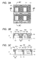
- FIG. 3A is a plan view for illustrating the photoelectric conversion apparatus of the first exemplary embodiment.
- FIG. 3B is a schematic sectional view for illustrating the photoelectric conversion apparatus of the first exemplary embodiment.
- FIG. 3C is a schematic sectional view for illustrating the photoelectric conversion apparatus of the first exemplary embodiment.
- FIG. 4A is a plan view of a photoelectric conversion apparatus of a second exemplary embodiment.
- FIG. 4B is a schematic sectional view of the photoelectric conversion apparatus of the second exemplary embodiment.
- FIG. 4C is a schematic sectional view of the photoelectric conversion apparatus of the second exemplary embodiment.
- FIG. 5A is a plan view of a photoelectric conversion apparatus for illustrating a modification of the first exemplary embodiment.
- FIG. 5B is a schematic sectional view of the photoelectric conversion apparatus for illustrating the modification of the first exemplary embodiment.
- FIG. 5C is a schematic sectional view of the photoelectric conversion apparatus for illustrating the modification of the first exemplary embodiment.
- FIG. 6A is a plan view of a photoelectric conversion apparatus of a third exemplary embodiment.
- FIG. 6B is a schematic sectional view of the photoelectric conversion apparatus of the third exemplary embodiment.
- FIG. 6C is a schematic sectional view of the photoelectric conversion apparatus of the third exemplary embodiment.
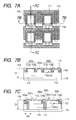
- FIG. 7A is a plan view of a photoelectric conversion apparatus for illustrating a modification of the third exemplary embodiment.
- FIG. 7B is a schematic sectional view of the photoelectric conversion apparatus for illustrating the modification of the third exemplary embodiment.
- FIG. 7C is a schematic sectional view of the photoelectric conversion apparatus for illustrating the modification of the third exemplary embodiment.
- FIGS. 8A, 8B, 8C, 8D, 8E, 8F and 8G are schematic sectional views for illustrating a method for manufacturing the photoelectric conversion apparatus of the first exemplary embodiment.
- FIGS. 9A, 9B, 9C, 9D, 9E, 9F and 9G are schematic sectional views for illustrating a method for manufacturing the photoelectric conversion apparatus of the first exemplary embodiment.
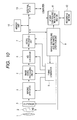
- FIG. 10 is a block diagram for illustrating an imaging system.
- FIGS. 11A, 11B, 11C, 11D and 11E are potential diagrams illustrating a potential of a path according to a fifth exemplary embodiment.
- a photoelectric conversion apparatus of the present invention includes a first semiconductor region, which functions as a barrier against signal charges, between a first and a second photoelectric conversion element; and a second semiconductor region, which functions as a barrier against signal charges and is narrower than the first semiconductor region, between the first and a third photoelectric conversion element. Further, a region with a low barrier (potential barrier) is provided at least a part between the first and the second photoelectric conversion element.
- This configuration can suppress that signal charges generated in the first photoelectric conversion element are unevenly mixed into the adjacent second and third photoelectric conversion elements. That is, the amount of signal charge mixing into the adjacent photoelectric conversion elements can be equalized, thereby improving image quality to be acquired. Further, when correction is made, an image signal can easily be corrected. Accordingly, a necessary configuration of an image processor can be simplified.
- FIG. 2A is a circuit diagram of an example of the pixel circuit to which the present invention can be applied.
- FIG. 2B is a plan view illustrating a planar layout of the pixel circuit for four pixels. A case where the signal charge is of electrons is described below.
- a pixel includes a photodiode 100, which is a photoelectric conversion element; a transferring MOS transistor 101; a reset MOS transistor 102; an amplifying MOS transistor 103; and a selection MOS transistor 105.
- the transferring MOS transistor 101 transfers signal charges generated in the photoelectric conversion element 100 to a floating diffusion region 104.
- the amplifying MOS transistor 103 outputs an output according to a potential of the floating diffusion region 104 to output line 106 via the selection MOS transistor 105.
- the amplifying MOS transistor 103 is a part of a source follower circuit. The gate electrode thereof is connected to the floating diffusion region 104.
- the reset MOS transistor 102 resets a node of the gate electrode of the amplifying MOS transistor 103, i.e. the floating diffusion region 104, to a prescribed potential (reset potential).
- the transferring MOS transistor 101 is supplied with a transfer control signal TX.
- the reset MOS transistor 102 is supplied with a reset control signal RES.
- the selection MOS transistor 105 is supplied with a selection control signal SEL. Each control signal controls the readout of the signal charge.
- such pixels are arranged one-dimensionally or two-dimensionally. This arrangement configures an imaging region.
- FIG. 2B illustrates a planar layout of four pixels (pixels a to d).
- four photodiodes 200 are arranged.
- a gate electrode 201 is of the transferring MOS transistor 101.
- a gate electrode 202 is of the reset MOS transistor 102.
- a gate electrode 203 is of the amplifying MOS transistor 103.
- a gate electrode 205 is of the selection MOS transistor 105.
- a source region 206 is of the reset MOS transistor.
- a drain region 207 is of the reset MOS transistor and of the amplifying MOS transistor.
- a source region 208 is of the amplifying MOS transistor, and is also a drain region of the selection MOS transistor.
- a source region 209 which is of the selection MOS transistor, is connected to the output line 106.
- the photoelectric conversion elements 200 in FIG. 2B are referred to as a first photoelectric conversion element 200a, a second photoelectric conversion element 200b, a third photoelectric conversion element 200c and a fourth photoelectric conversion element 200d.
- symbols are assigned only to the pixel d.
- the gate electrode of the transferring MOS transistor corresponding to the photoelectric conversion element 200d is represented with reference numeral 201d. Since configurations are identical among other pixels, symbols are omitted.
- An element isolation region 210 defines active regions 211 and 212.
- a LOCOS (local oxidation of silicon) structure is used for the element isolation region 210 of the elements.
- the structure may be STI (shallow trench isolation) structure instead.
- the element isolation region 210 may be a structure where only a semiconductor region functioning as a barrier against a signal charge is arranged (diffusion isolation). If the element isolation region 210 includes only the semiconductor region functioning as the barrier against the signal charges, the active region is defined at a boundary with the semiconductor region functioning as the barrier against the signal charge.
- the active region 211 includes the photoelectric conversion element 200 and a floating diffusion region 204.
- the active region 212 includes the source region and the drain region of each transistor.
- a distance between the active region 211a where the photoelectric conversion element 200a is arranged and the active region 211b where the photoelectric conversion element 200b is arranged, or the width of a first region 213 between the photoelectric conversion elements 200a and 200b is represented as a first width W1.
- a distance between the active region 211a where the photoelectric conversion element 200a is arranged and the active region 211c where the photoelectric conversion element 200c is arranged, or the width of a second region 214 between the photoelectric conversion elements 200a and 200c is represented as a second width W2.
- the first width W1 and the second width W2 are different from each other, and W1 > W2.
- the pixels are arranged in a matrix manner along a first direction (X axis) and a second direction (Y axis). The first and second directions are orthogonal to each other.
- the photoelectric conversion apparatus is not limited to the circuit as illustrated in FIG. 2A .
- the apparatus may be a configuration where a larger number of photoelectric conversion elements share the amplifying MOS transistor, or a configuration without the selection MOS transistor. Further, the configuration is not limited to the planar layout as illustrated in FIG. 2B . Exemplary embodiments of the present invention are hereinafter described using the figures.
- FIG. 1A is a plan view corresponding to the plan view of FIG. 2B .
- symbols for elements similar to those of FIG. 2B are omitted. Symbols are assigned only to parts characterizing this exemplary embodiment.
- FIG. 1A there are arranged a first semiconductor region 110 and a second semiconductor region 111.
- the regions 110 and 111 are a first conductive type (P type), where signal charges become a minority carrier, and configure barriers against the signal charges (electrons). More specifically, the first semiconductor region 110 with a third width W3 is arranged in the first region 213.
- P type first conductive type
- the second semiconductor region 111 with a fourth width W4 is arranged in the second region 214. These arrangements form potential barriers.
- the first semiconductor region 110 is arranged under an active region 211 where a transistor is arranged.
- a third semiconductor region 112 is arranged at a part of the first region 213.
- the region 112 is the first conductive type with the third width W3.
- the third semiconductor region 112 has a potential lower than a potential of the first semiconductor region 110. Because, an impurity concentration of the third semiconductor region 112 is lower than that of the first semiconductor region 110. More specifically, the third semiconductor region 112 is arranged under the source region 206 of the reset MOS transistor.
- the first to third semiconductor regions form a grid-like potential barrier surrounding the photoelectric conversion element.
- the amount of charge flowing from the photoelectric conversion element 200a into the photoelectric conversion elements 200b and 200c can be equalized, by arranging the third semiconductor region 112, while the charge flowing from the photoelectric conversion element 200a into the adjacent photoelectric conversion elements is suppressed.
- FIGS. 1B and 1C are schematic sectional views of FIG. 1A taken along XX' and YY' lines, respectively.
- elements with the same configurations are assigned with the same symbols, and the description thereof is omitted.
- FIGS. 1B and 1C there are a first conductive substrate 115, a first conductive type semiconductor region 114 and a plane 119 including a light receiving surface of the photoelectric conversion element.
- the conductive type of the substrate 115 is arbitrary.
- the semiconductor region 114 may be the second conductive type, a layer formed on the substrate 115 by epitaxial growth, or a layer formed by ion implementation into the substrate 115. With reference to the plane 119, a direction toward the substrate 115 is a depth direction at the substrate.
- the element isolation region 210 includes a LOCOS structure 113.
- the photoelectric conversion element 200 includes a second conductive type (N type) charge accumulation region 116 and a P type surface protective layer 117 arranged on a side of the light receiving surface 119 of the photoelectric conversion element.
- the second semiconductor region 111 has the width W4 and a depth D1.
- the third semiconductor region 112 has the width W3 and the depth D1.
- the first semiconductor region 110 arranged in the first region 213 has a configuration with the width W3 and the depth D1.
- the widths and the depths of the first semiconductor region 110 and the third semiconductor region 112 arranged in the first region 213 are set identical to each other.
- the impurity concentration of the third semiconductor region is set lower than the impurity concentrations of the first and second semiconductor regions.
- the impurity concentration of the third semiconductor region 112 can appropriately be set by means of the layout of the photoelectric conversion apparatus and the widths W3 and W4 of the first semiconductor region.
- FIGS. 3A to 3C are figures corresponding to FIGS. 1A to 1C , and based on FIG. 2B as with FIG. 1A .
- same elements as those in FIGS. 1A to 1C or FIG. 2B are assigned with the same symbols, and the description thereof is omitted.
- the third semiconductor region provided in FIGS. 1A to 1C is not provided in FIGS. 3A to 3C .
- the first semiconductor region 110 and the second semiconductor region 111 are provided in FIGS. 3A to 3C .
- the path 1 is formed.
- the signal charges are more likely to flow into the adjacent photoelectric conversion element through the path 1 than the path 2.
- the mixing amount of signal charge to the adjacent photoelectric conversion element that becomes uneven owing to the paths 2 and a path 3 can be adjusted even by the path 1.
- likelihood of flowing of the signal charges into the adjacent photoelectric conversion element is determined according to the height of the potential with respect to the signal charge, i.e. the height of the potential barrier.
- the potential barrier of the path 3 is lower than the potential barrier of the path 2.
- the potential barrier of the path 1 is lower than the potential barrier of the path 3.
- the third semiconductor region 112 with the low impurity concentration is arranged in at least one part between the photoelectric conversion elements where the semiconductor region with a wide width is arranged.
- the charges to flow from the photoelectric conversion element 200a into the adjacent photoelectric conversion element can be suppressed.
- the amount of charge flowing from the photoelectric conversion element 200a into the photoelectric conversion elements 200b and 200c can be equalized.
- At least one part between the photoelectric conversion elements where the semiconductor region with the wide width is arranged may be a part of the semiconductor region with the wide width. That is, a configuration where the third semiconductor region is formed in the first semiconductor region may be adopted.
- FIGS. 8A to 8G are diagrams illustrating a manufacturing process using a sectional view corresponding to FIG. 1B .
- FIGS. 9A to 9G are diagrams illustrating the manufacturing process using a sectional view corresponding to FIG. 1C .
- N type epitaxial layer 114' is formed on the N type substrate 115.
- LOCOS 113 is formed and the active region is formed ( FIGS. 8B and 9B ).
- ion implementation is performed using a photoresist mask, and a P type fourth semiconductor region 120 is formed at an end of the LOCOS 113.
- FIGS. 8D and 9D ion implementation of a desired amount of dose is performed using a photoresist mask, and the P type first semiconductor region 110 and the second semiconductor region 111 are formed.
- ion implementation of a smaller amount of dose than that in FIGS. 8D and 9D is performed using another photoresist mask, and the P type third semiconductor region 112 is formed ( FIGS. 8E and 9E ).
- the gate electrode of the transistor is formed by patterning ( FIGS. 8F and 9F ). Subsequently, the N type charge accumulation region 116 and the P type surface protective layer 117 of the photoelectric conversion element are formed, and the source region and the drain region of the transistor are formed ( FIGS. 8G and 9G ).
- the fourth semiconductor region 113 is arranged between the insulator of the element isolation region, or LOCOS 113 here, and the photoelectric conversion element 200, and covers the surface of the photoelectric conversion element 200. This fourth semiconductor region 113 enables mixing of dark current generated in the element isolation region into the photoelectric conversion element to be reduced.
- the third semiconductor region may be provided under the gate electrode of the transistor as illustrated in FIGS. 5A to 5C.
- FIG. 5A corresponds to FIG. 1A .
- FIGS. 5B and 5C are schematic sectional views taken along the lines XX' and YY' in FIG. 5A , respectively.
- elements similar to those in FIGS. 1A to 1C are assigned with the same symbols, and the description thereof is omitted.
- the third semiconductor region 512 is provide under the gate electrode 203 of the amplifying MOS transistor, instead of the source region of the reset MOS transistor. Even with such an arrangement, the amount of charge flowing from the photoelectric conversion element 200a into the photoelectric conversion elements 200b and 200c can be equalized, while the charges to flow from the photoelectric conversion element 200a into the adjacent photoelectric conversion elements are suppressed.
- the third semiconductor region is provided under the source region of the reset MOS transistor. Note that, also in the source region of another transistor, the third semiconductor region may be arranged under the drain region.
- FIGS. 4A, 4B and 4C A photoelectric conversion apparatus of this exemplary embodiment is described using FIGS. 4A, 4B and 4C.
- FIG. 4A corresponds to FIG. 1A .
- FIGS. 4B and 4C are schematic sectional views taken along the lines XX' and YY' in FIG. 4A , respectively.
- elements similar to those in FIGS. 1A to 1C are assigned with the same symbols, and the description thereof is omitted. Only a configuration in this exemplary embodiment different from that of the first exemplary embodiment is hereinafter described.
- the part with low potential barrier is formed by the impurity concentration.
- a part with low potential barrier is formed by the width of the semiconductor region forming the potential barrier.
- the photoelectric conversion apparatus of this exemplary embodiment includes the first semiconductor region 110 with the width W3 and the second semiconductor region 111 with the width W4, as with the first exemplary embodiment. Further, a third semiconductor region 412 of the first conductive type with a fifth width W5 narrower than the width W4 is provided.
- the first semiconductor region 110, the second semiconductor region 111 and the third semiconductor region 412 have the same impurity concentration and the depth D1.
- a path 4 passing through the third semiconductor region 412 is provided instead of the path 3 of the first exemplary embodiment. Accordingly, the mixing amount of signal charge to the adjacent photoelectric conversion element can evenly be adjusted.
- the third semiconductor region 412 with the narrow width is arranged in at least a part of the region with wide width. According to such a configuration, the charges to flow from the photoelectric conversion element 200a into the adjacent photoelectric conversion elements can be suppressed. Further, according to this configuration, the amount of charge flowing from the photoelectric conversion element 200a into the photoelectric conversion element 200b and the amount of charge flowing from the photoelectric conversion element 200a into the photoelectric conversion element 200c can be equalized.
- the process of forming the first to third semiconductor regions is simplified in comparison with the first exemplary embodiment. That is, provided that the shape of the photoresist mask is formed in a desired form, the first to third semiconductor regions can be formed by the same ion implementation process.
- FIGS. 6A, 6B and 6C A photoelectric conversion apparatus of this exemplary embodiment is described using FIGS. 6A, 6B and 6C.
- FIG. 6A corresponds to FIG. 1A .
- FIGS. 6B and 6C are schematic sectional views taken along the lines XX' and YY' in FIG. 6A , respectively.
- elements similar to those in FIGS. 1A to 1C are assigned with the same symbols, and the description thereof is omitted. Only a configuration in this exemplary embodiment different from that of the first exemplary embodiment is hereinafter described.
- the part with low potential barrier is formed by the impurity concentration.
- the photoelectric conversion apparatus of this exemplary embodiment includes the first semiconductor region 110 and the second semiconductor region 111, as with the first exemplary embodiment.
- a third region 612 without the first conductive type semiconductor region is formed in the region 212 where the first semiconductor region 110 is arranged.
- the first semiconductor region 110 and the second semiconductor region 111 have the same impurity concentration, and the same depth D1.
- a path 5 passing through the third region 612 is provided instead of the path 3 of the first exemplary embodiment. Accordingly, the mixing amount of signal charge to the adjacent photoelectric conversion element can uniformly be adjusted.
- Table 1 illustrates a comparison of mixing amounts of signal charge to the adjacent photoelectric conversion elements in the configurations in FIGS. 6A to 6C and 3A to 3C .
- the mixing amount of signal charge from the photoelectric conversion element 200a to the photoelectric conversion element 200c is represented as a mixing amount of charge 1.
- the mixing amount of signal charge from the photoelectric conversion element 200a to the photoelectric conversion element 200b is represented as the mixing amount of charge 2.
- the unit of the mixing amounts of charge is arbitrary.
- the configuration in FIGS. 6A to 6C reduces the difference between the mixing amounts of charge 1 and 2.
- the difference between the mixing amounts of charge 1 and 2 can further be reduced by thorough consideration in designing.
- the semiconductor region with different width functioning as the barrier against the signal charge is thus arranged between the photoelectric conversion elements as in FIG. 2B , at least a part of the semiconductor region with the wide width is chipped (not provided). According to such a configuration, the charges to flow from the photoelectric conversion element 200a to the adjacent photoelectric conversion elements can be suppressed. Further, the amount of charge flowing from the photoelectric conversion element 200a into the photoelectric conversion element 200b and the amount of charge flowing from the photoelectric conversion element 200a into the photoelectric conversion element 200c can be equalized.
- a region 712 corresponding to the region 612 may be arranged under the source region or the drain region of the transistor.
- the region may be arranged under the source region, the drain region or the semiconductor region to which a fixed potential, such as a power source or a ground, is supplied.
- a fixed potential such as a power source or a ground
- the process of forming the first and second semiconductor regions and the third region 612 is simplified in comparison with the first exemplary embodiment. That is, as to the mask pattern of the ion implementation for forming the first and second semiconductor regions, a pattern where no opening is provided in the third region 612 is used. Accordingly, the first and second semiconductor regions and the region 612 of this exemplary embodiment can be formed.
- FIG. 10 illustrates a block diagram in a case of applying the photoelectric conversion apparatus to the digital camera as an example of the imaging system.
- the system includes a barrier 1 for protecting a lens, a lens 2 forming an optical image of a subject at the imaging apparatus 4 (photoelectric conversion apparatus), and a diaphragm 3 for changing the amount of light passing through the lens 2.
- the system also includes an A/D converter 6 performing analog/digital conversion on image signal output from the imaging apparatus 4, and a signal processing unit 7 applying various corrections to the image data output from the A/D converter 6 and compressing the same data.
- the system further includes a timing generator 8 outputting various timing signals to the imaging apparatus 4, the image signal processing circuit 5, the A/D converter 6 and the signal processing unit 7.
- the system includes a whole controlling and arithmetic operation unit 9 that performs various operations and totally controls the digital camera.
- the system includes a memory unit 10 for temporarily storing the image data, an interface 11 for recording and reading a data on or from the recording medium, and a detachable recording medium 12, such as a semiconductor memory, for recording and reading the image data. Further, the system includes an interface 13 for communicating with an external computer.
- the timing signal may be input from the outside.
- the imaging system may include at least the imaging apparatus 4 and the signal processing unit 7 processing the image signal output from the imaging apparatus.
- the timing generator or the A/D converter may be formed on the same substrate as that of the imaging apparatus.
- the photoelectric conversion apparatus of the present invention may be applied to the imaging system. A high quality image can be acquired by applying the photoelectric conversion apparatus of the present invention to the imaging system.
- FIG. 11A illustrates schematically a potential configuration as to a signal charge (electron herein) in the path 1 in FIG. 1B .
- FIG. 11B illustrates schematically a potential configuration as to the signal charge in the path 2 in FIG. 3B .
- FIG. 11C illustrates schematically a potential configuration as to the signal charge in the path 4 in FIG. 4B .
- FIG. 11D illustrates schematically a potential configuration as to the signal charge in the path 5 in FIG. 6B .
- FIG. 11E illustrates schematically a potential configuration as to the signal charge in the path 3 in FIG. 1C .
- a potential P1 in the charge accumulation region 116 of N type semiconductor region is at a lowest state as to the electron.
- a potential P2 in the semiconductor region 114 of P type is higher than the potential P1.
- a potential P3 in the third semiconductor region 112 of the width W3 is higher than the potential P2.
- a potential P4 in the first semiconductor region 110 of the width W3 is higher than the potential P3.
- the potential of the third semiconductor region 112 is lower.
- the second semiconductor region 111 of the width W4 narrower than W3 is at the potential P4.
- the first semiconductor region 110 in the path 2 is at the same potential 4 as the potential of the second semiconductor region 111 in the path 3.
- the first semiconductor region 110 in the path 2 has the width W3 broader than the width of the second semiconductor region 111 in the path 3. Accordingly, the signal charge is hardly transported through or over the path 2 rather than the path 3.
- the third semiconductor region 112 in the path 1 has the same width W3 as that of the first semiconductor region 110 in the path 2.
- the third semiconductor region 112 in the path 1 is at the potential P3 lower than the potential of the first semiconductor region 110 in the path 2. Accordingly, the signal charge is easily transported through or over the path 1 rather than the path 2.
- a quantity of mixing of the signal charge can be adjusted.
- the third semiconductor region 412 has a width W5 narrower than the width W4, and is at the potential P4.
- the first semiconductor region 110 in the path 2 is at the same potential P4 as that of the third semiconductor region 412 in the path 4.
- the first semiconductor region 110 in the path 2 has a width W3 broader than that of the third semiconductor region 412 in the path 4. That is, the signal charge is easily transported through or over the path 4 rather than the path 2.
- the third semiconductor region 412 in the path 4 is at the same potential P4 as that of the second semiconductor region 111 in the path 3.
- the third semiconductor region 412 in the path 4 has the width W5 narrower than that of the second semiconductor region 111 in the path 3. Accordingly, the signal charge is easily transported through or over the path 4 rather than the path 3.
- the path 4 is a part of the first region, that is, the first semiconductor region 110 is partially replaced with the third semiconductor region 412, the quantity of mixing the signal charge can be adjusted.
- the first semiconductor region 110 in the path 2 is at the potential P4. While, the third semiconductor region 612 in the path 5 is at the potential P2. Accordingly, the signal charge is easily transported through the path 5 rather than the path 2.
- the second semiconductor region 111 in the path 3 is at the potential P4. While, the third semiconductor region 612 in the path 5 is at the potential P2. Accordingly, the signal charge is easily transported through the path 5 rather than the path 3.
- the barrier at least one part of the semiconductor region with the wide width is made to be low. This configuration can suppress that the signal charges generated in a certain photoelectric conversion element are unevenly mixed into any photoelectric conversion element among the adjacent photoelectric conversion elements.
- the configuration reducing a part of potential is a configuration where a part of impurity concentration of the semiconductor region functioning as a barrier is reduced, the width is narrowed or the depth is reduced, or a configuration where a part of the semiconductor region functioning as the barrier is not provided.
- a photoelectric conversion apparatus of the present invention includes a first semiconductor region functioning as a barrier against signal charges between a first and a second photoelectric conversion element, and a second semiconductor region that has a width narrower than that of the first semiconductor region and functions as a barrier against signal charges between a first and the third photoelectric conversion element.
- a region with a low barrier is provided at least a part between the first and the second photoelectric conversion element.
Landscapes
- Engineering & Computer Science (AREA)
- Multimedia (AREA)
- Signal Processing (AREA)
- Solid State Image Pick-Up Elements (AREA)
- Light Receiving Elements (AREA)
- Transforming Light Signals Into Electric Signals (AREA)
Abstract
Description
- The present application relates to a structure of separation of a photoelectric conversion apparatus.
- CCD type and CMOS type photoelectric conversion apparatuses are used for many digital cameras and digital camcorders. In recent years, in the photoelectric conversion apparatuses, pixels have been reduced. Accordingly, measures against mixing of charges to adjacent pixels (crosstalk) have been discussed.
- Japanese Patent Application Laid-Open No.
2003-258232 - However, even with the P type well region disclosed in Japanese Patent Application Laid-Open No.
2003-258232 - It is an object of the present invention to provide a photoelectric conversion apparatus capable of reducing variation in charges mixing into the adjacent photoelectric conversion elements (pixels).
- A photoelectric conversion apparatus according to the present invention includes: a substrate; a plurality of photoelectric conversion elements arranged on the substrate; and a transistor arranged on the substrate for transferring a signal charge generated by the photoelectric conversion element, wherein the plurality of photoelectric conversion elements include a first photoelectric conversion element, a second photoelectric conversion element adjacent to the first photoelectric conversion element and a third photoelectric conversion element adjacent to the first photoelectric conversion element, and a first region having a first width is arranged between the first and second photoelectric conversion elements, a second region having a second width narrower than the first width is arranged between the first and third photoelectric conversion elements, a first semiconductor region of a first conductivity type such that the signal charge is minority carrier and of a third width is arranged in the first region, a second semiconductor region of the first conductivity type and of a fourth width narrower than the third width is arranged in the second region, and a third region at a potential as to the signal charge lower than first region is arranged in the first region.
- Other features and advantages of the present invention will be apparent from the following description taken in conjunction with the accompanying drawings, in which like reference characters designate the same or similar parts throughout the figures thereof.
- Further features of the present invention will become apparent from the following description of exemplary embodiments with reference to the attached drawings.
-
FIG. 1A is a plan view of a photoelectric conversion apparatus of a first exemplary embodiment. -
FIG. 1B is a schematic sectional view of the photoelectric conversion apparatus of the first exemplary embodiment. -
FIG. 1C is a schematic sectional view of the photoelectric conversion apparatus of the first exemplary embodiment. -
FIG. 2A illustrates an example of a pixel circuit of the photoelectric conversion apparatus. -
FIG. 2B is a plan view of the pixel circuit of the photoelectric conversion apparatus. -
FIG. 3A is a plan view for illustrating the photoelectric conversion apparatus of the first exemplary embodiment. -
FIG. 3B is a schematic sectional view for illustrating the photoelectric conversion apparatus of the first exemplary embodiment. -
FIG. 3C is a schematic sectional view for illustrating the photoelectric conversion apparatus of the first exemplary embodiment. -
FIG. 4A is a plan view of a photoelectric conversion apparatus of a second exemplary embodiment. -
FIG. 4B is a schematic sectional view of the photoelectric conversion apparatus of the second exemplary embodiment. -
FIG. 4C is a schematic sectional view of the photoelectric conversion apparatus of the second exemplary embodiment. -
FIG. 5A is a plan view of a photoelectric conversion apparatus for illustrating a modification of the first exemplary embodiment. -
FIG. 5B is a schematic sectional view of the photoelectric conversion apparatus for illustrating the modification of the first exemplary embodiment. -
FIG. 5C is a schematic sectional view of the photoelectric conversion apparatus for illustrating the modification of the first exemplary embodiment. -
FIG. 6A is a plan view of a photoelectric conversion apparatus of a third exemplary embodiment. -
FIG. 6B is a schematic sectional view of the photoelectric conversion apparatus of the third exemplary embodiment. -
FIG. 6C is a schematic sectional view of the photoelectric conversion apparatus of the third exemplary embodiment. -
FIG. 7A is a plan view of a photoelectric conversion apparatus for illustrating a modification of the third exemplary embodiment. -
FIG. 7B is a schematic sectional view of the photoelectric conversion apparatus for illustrating the modification of the third exemplary embodiment. -
FIG. 7C is a schematic sectional view of the photoelectric conversion apparatus for illustrating the modification of the third exemplary embodiment. -
FIGS. 8A, 8B, 8C, 8D, 8E, 8F and 8G are schematic sectional views for illustrating a method for manufacturing the photoelectric conversion apparatus of the first exemplary embodiment. -
FIGS. 9A, 9B, 9C, 9D, 9E, 9F and 9G are schematic sectional views for illustrating a method for manufacturing the photoelectric conversion apparatus of the first exemplary embodiment. -
FIG. 10 is a block diagram for illustrating an imaging system. -
FIGS. 11A, 11B, 11C, 11D and 11E are potential diagrams illustrating a potential of a path according to a fifth exemplary embodiment. - The accompanying drawings, which are incorporated in and constitute a part of the specification, illustrate embodiments of the invention and, together with the description, serve to explain the principles of the invention.
- Preferred embodiments of the present invention will now be described in detail in accordance with the accompanying drawings.
- A photoelectric conversion apparatus of the present invention includes a first semiconductor region, which functions as a barrier against signal charges, between a first and a second photoelectric conversion element; and a second semiconductor region, which functions as a barrier against signal charges and is narrower than the first semiconductor region, between the first and a third photoelectric conversion element. Further, a region with a low barrier (potential barrier) is provided at least a part between the first and the second photoelectric conversion element. This configuration can suppress that signal charges generated in the first photoelectric conversion element are unevenly mixed into the adjacent second and third photoelectric conversion elements. That is, the amount of signal charge mixing into the adjacent photoelectric conversion elements can be equalized, thereby improving image quality to be acquired. Further, when correction is made, an image signal can easily be corrected. Accordingly, a necessary configuration of an image processor can be simplified.
- An embodiment of the present invention is hereinafter described in detail using the figures.
- (Example of Pixel Circuit)
- An example of a pixel circuit to which the present invention can be applied is described.
FIG. 2A is a circuit diagram of an example of the pixel circuit to which the present invention can be applied.FIG. 2B is a plan view illustrating a planar layout of the pixel circuit for four pixels. A case where the signal charge is of electrons is described below. - In
FIG. 2A , a pixel (PIXEL) includes aphotodiode 100, which is a photoelectric conversion element; a transferringMOS transistor 101; areset MOS transistor 102; an amplifyingMOS transistor 103; and aselection MOS transistor 105. The transferringMOS transistor 101 transfers signal charges generated in thephotoelectric conversion element 100 to a floatingdiffusion region 104. The amplifyingMOS transistor 103 outputs an output according to a potential of the floatingdiffusion region 104 tooutput line 106 via theselection MOS transistor 105. The amplifyingMOS transistor 103 is a part of a source follower circuit. The gate electrode thereof is connected to the floatingdiffusion region 104. Thereset MOS transistor 102 resets a node of the gate electrode of the amplifyingMOS transistor 103, i.e. the floatingdiffusion region 104, to a prescribed potential (reset potential). The transferringMOS transistor 101 is supplied with a transfer control signal TX. Thereset MOS transistor 102 is supplied with a reset control signal RES. Theselection MOS transistor 105 is supplied with a selection control signal SEL. Each control signal controls the readout of the signal charge. In the photoelectric conversion apparatus, such pixels are arranged one-dimensionally or two-dimensionally. This arrangement configures an imaging region. -
FIG. 2B illustrates a planar layout of four pixels (pixels a to d). InFIG. 2B , four photodiodes 200 are arranged. A gate electrode 201 is of the transferringMOS transistor 101. A gate electrode 202 is of thereset MOS transistor 102. A gate electrode 203 is of the amplifyingMOS transistor 103. A gate electrode 205 is of theselection MOS transistor 105. There is a floating diffusion region 204. Further, a source region 206 is of the reset MOS transistor. A drain region 207 is of the reset MOS transistor and of the amplifying MOS transistor. A source region 208 is of the amplifying MOS transistor, and is also a drain region of the selection MOS transistor. A source region 209, which is of the selection MOS transistor, is connected to theoutput line 106. Hereinafter, for the sake of description, the photoelectric conversion elements 200 inFIG. 2B are referred to as a firstphotoelectric conversion element 200a, a secondphotoelectric conversion element 200b, a thirdphotoelectric conversion element 200c and a fourthphotoelectric conversion element 200d. In a configuration other than that of the photoelectric conversion element, symbols are assigned only to the pixel d. For example, the gate electrode of the transferring MOS transistor corresponding to thephotoelectric conversion element 200d is represented withreference numeral 201d. Since configurations are identical among other pixels, symbols are omitted. - An
element isolation region 210 defines active regions 211 and 212. In this embodiment, a LOCOS (local oxidation of silicon) structure is used for theelement isolation region 210 of the elements. However, the structure may be STI (shallow trench isolation) structure instead. Further, theelement isolation region 210 may be a structure where only a semiconductor region functioning as a barrier against a signal charge is arranged (diffusion isolation). If theelement isolation region 210 includes only the semiconductor region functioning as the barrier against the signal charges, the active region is defined at a boundary with the semiconductor region functioning as the barrier against the signal charge. InFIG. 2B , the active region 211 includes the photoelectric conversion element 200 and a floating diffusion region 204. The active region 212 includes the source region and the drain region of each transistor. Here, inFIG. 2B , a distance between the active region 211a where thephotoelectric conversion element 200a is arranged and the active region 211b where thephotoelectric conversion element 200b is arranged, or the width of afirst region 213 between thephotoelectric conversion elements photoelectric conversion element 200a is arranged and the active region 211c where thephotoelectric conversion element 200c is arranged, or the width of asecond region 214 between thephotoelectric conversion elements - The photoelectric conversion apparatus is not limited to the circuit as illustrated in
FIG. 2A . The apparatus may be a configuration where a larger number of photoelectric conversion elements share the amplifying MOS transistor, or a configuration without the selection MOS transistor. Further, the configuration is not limited to the planar layout as illustrated inFIG. 2B . Exemplary embodiments of the present invention are hereinafter described using the figures. - (First Exemplary Embodiment)
- A photoelectric conversion apparatus of this exemplary embodiment is described using
FIGS. 1A to 1C . First,FIG. 1A is a plan view corresponding to the plan view ofFIG. 2B . InFIG. 1A , symbols for elements similar to those ofFIG. 2B are omitted. Symbols are assigned only to parts characterizing this exemplary embodiment. InFIG. 1A , there are arranged afirst semiconductor region 110 and asecond semiconductor region 111. Theregions first semiconductor region 110 with a third width W3 is arranged in thefirst region 213. Thesecond semiconductor region 111 with a fourth width W4 is arranged in thesecond region 214. These arrangements form potential barriers. Thefirst semiconductor region 110 is arranged under an active region 211 where a transistor is arranged. Athird semiconductor region 112 is arranged at a part of thefirst region 213. Theregion 112 is the first conductive type with the third width W3. Thethird semiconductor region 112 has a potential lower than a potential of thefirst semiconductor region 110. Because, an impurity concentration of thethird semiconductor region 112 is lower than that of thefirst semiconductor region 110. More specifically, thethird semiconductor region 112 is arranged under the source region 206 of the reset MOS transistor. The first to third semiconductor regions form a grid-like potential barrier surrounding the photoelectric conversion element. Here, the amount of charge flowing from thephotoelectric conversion element 200a into thephotoelectric conversion elements third semiconductor region 112, while the charge flowing from thephotoelectric conversion element 200a into the adjacent photoelectric conversion elements is suppressed. - The configuration in
FIG. 1A is further described usingFIGS. 1B and 1C. FIGS. 1B and 1C are schematic sectional views ofFIG. 1A taken along XX' and YY' lines, respectively. InFIGS. 1B and 1C , elements with the same configurations are assigned with the same symbols, and the description thereof is omitted. InFIGS. 1B and 1C , there are a firstconductive substrate 115, a first conductivetype semiconductor region 114 and aplane 119 including a light receiving surface of the photoelectric conversion element. Here, the conductive type of thesubstrate 115 is arbitrary. Thesemiconductor region 114 may be the second conductive type, a layer formed on thesubstrate 115 by epitaxial growth, or a layer formed by ion implementation into thesubstrate 115. With reference to theplane 119, a direction toward thesubstrate 115 is a depth direction at the substrate. InFIGS. 1B and 1C , theelement isolation region 210 includes aLOCOS structure 113. InFIGS. 1B and 1C , the photoelectric conversion element 200 includes a second conductive type (N type) charge accumulation region 116 and a P type surface protective layer 117 arranged on a side of thelight receiving surface 119 of the photoelectric conversion element. - In
FIG. 1C , thesecond semiconductor region 111 has the width W4 and a depth D1. In the sectional view ofFIG. 1B , thethird semiconductor region 112 has the width W3 and the depth D1. Thefirst semiconductor region 110 arranged in thefirst region 213 has a configuration with the width W3 and the depth D1. In this exemplary embodiment, the widths and the depths of thefirst semiconductor region 110 and thethird semiconductor region 112 arranged in thefirst region 213 are set identical to each other. The impurity concentration of the third semiconductor region is set lower than the impurity concentrations of the first and second semiconductor regions. The impurity concentration of thethird semiconductor region 112 can appropriately be set by means of the layout of the photoelectric conversion apparatus and the widths W3 and W4 of the first semiconductor region. - Here, a flow of the signal charges is described using
FIGS. 3A to 3C. FIGS. 3A to 3C are figures corresponding toFIGS. 1A to 1C , and based onFIG. 2B as withFIG. 1A . InFIGS. 3A to 3C , same elements as those inFIGS. 1A to 1C orFIG. 2B are assigned with the same symbols, and the description thereof is omitted. The third semiconductor region provided inFIGS. 1A to 1C is not provided inFIGS. 3A to 3C . Thefirst semiconductor region 110 and thesecond semiconductor region 111 are provided inFIGS. 3A to 3C . In such a configuration, when the signal charges flow into the adjacent photoelectric conversion elements, the charges flow via thepath 2 with the width W3 passing through thefirst semiconductor region 110, and via thepath 3 with the width W4 passing through thesecond semiconductor region 111. Here, since thefirst semiconductor region 110 and thesecond semiconductor region 111 have the same impurity concentration and the same depth, the probability that the signal charges flow into the adjacent photoelectric conversion elements via thepath 3 are higher than that via thepath 2. Accordingly, even in the adjacent photoelectric conversion element, a mixing amount of signal charge generated in thephotoelectric conversion element 200a is larger in thephotoelectric conversion element 200c than that inphotoelectric conversion element 200b, thereby causing unevenness. That is, in a monochrome photoelectric conversion apparatus, unevenness occurs in image quality. In a single panel color photoelectric conversion apparatus for a camera, the adjacent photoelectric conversion element generates a different color signal, thereby causing cross talk (color mixture). - On the other hand, according to the configuration illustrated in
FIGS. 1A to 1C , since the third semiconductor region with the low impurity concentration is provided, thepath 1 is formed. The signal charges are more likely to flow into the adjacent photoelectric conversion element through thepath 1 than thepath 2. The mixing amount of signal charge to the adjacent photoelectric conversion element that becomes uneven owing to thepaths 2 and apath 3 can be adjusted even by thepath 1. Here, likelihood of flowing of the signal charges into the adjacent photoelectric conversion element is determined according to the height of the potential with respect to the signal charge, i.e. the height of the potential barrier. Here, the potential barrier of thepath 3 is lower than the potential barrier of thepath 2. The potential barrier of thepath 1 is lower than the potential barrier of thepath 3. That is, if there is a semiconductor region with a different width functioning as a potential barrier between the photoelectric conversion elements, a part of the potential barrier with a wider width is made to have a lower potential barrier. Accordingly, the mixing amount of the signal charge can be equalized. - In this exemplary embodiment, the
third semiconductor region 112 with the low impurity concentration is arranged in at least one part between the photoelectric conversion elements where the semiconductor region with a wide width is arranged. According to such a configuration, the charges to flow from thephotoelectric conversion element 200a into the adjacent photoelectric conversion element can be suppressed. Further, the amount of charge flowing from thephotoelectric conversion element 200a into thephotoelectric conversion elements - Next, a method for manufacturing the photoelectric conversion apparatus of this exemplary embodiment is described using
FIGS. 8A to 8G and9A to 9G .FIGS. 8A to 8G are diagrams illustrating a manufacturing process using a sectional view corresponding toFIG. 1B .FIGS. 9A to 9G are diagrams illustrating the manufacturing process using a sectional view corresponding toFIG. 1C . - First, as illustrated in
FIGS. 8A and9A , N type epitaxial layer 114' is formed on theN type substrate 115. Next,LOCOS 113 is formed and the active region is formed (FIGS. 8B and9B ). InFIGS. 8C and9C , ion implementation is performed using a photoresist mask, and a P typefourth semiconductor region 120 is formed at an end of theLOCOS 113. - Next, ion implementation of a desired amount of dose is performed using a photoresist mask, and the P type
first semiconductor region 110 and thesecond semiconductor region 111 are formed (FIGS. 8D and9D ). Next, ion implementation of a smaller amount of dose than that inFIGS. 8D and9D is performed using another photoresist mask, and the P typethird semiconductor region 112 is formed (FIGS. 8E and9E ). - Next, the gate electrode of the transistor is formed by patterning (
FIGS. 8F and9F ). Subsequently, the N type charge accumulation region 116 and the P type surface protective layer 117 of the photoelectric conversion element are formed, and the source region and the drain region of the transistor are formed (FIGS. 8G and9G ). - Subsequently, an insulating film and wirings are formed on the
light receiving surface 119, and inner-layer lenses, color filters and micro lenses (not shown) are formed. Thus, the photoelectric conversion apparatus is finished. - The
fourth semiconductor region 113 is arranged between the insulator of the element isolation region, orLOCOS 113 here, and the photoelectric conversion element 200, and covers the surface of the photoelectric conversion element 200. Thisfourth semiconductor region 113 enables mixing of dark current generated in the element isolation region into the photoelectric conversion element to be reduced. - As an application of this exemplary embodiment, the third semiconductor region may be provided under the gate electrode of the transistor as illustrated in
FIGS. 5A to 5C. FIG. 5A corresponds toFIG. 1A .FIGS. 5B and 5C are schematic sectional views taken along the lines XX' and YY' inFIG. 5A , respectively. InFIGS. 5A, 5B and 5C , elements similar to those inFIGS. 1A to 1C are assigned with the same symbols, and the description thereof is omitted. InFIGS. 5A, 5B and 5C , thethird semiconductor region 512 is provide under the gate electrode 203 of the amplifying MOS transistor, instead of the source region of the reset MOS transistor. Even with such an arrangement, the amount of charge flowing from thephotoelectric conversion element 200a into thephotoelectric conversion elements photoelectric conversion element 200a into the adjacent photoelectric conversion elements are suppressed. - In this exemplary embodiment, the third semiconductor region is provided under the source region of the reset MOS transistor. Note that, also in the source region of another transistor, the third semiconductor region may be arranged under the drain region.
- (Second Exemplary Embodiment)
- A photoelectric conversion apparatus of this exemplary embodiment is described using
FIGS. 4A, 4B and 4C. FIG. 4A corresponds toFIG. 1A .FIGS. 4B and 4C are schematic sectional views taken along the lines XX' and YY' inFIG. 4A , respectively. InFIGS. 4A, 4B and 4C , elements similar to those inFIGS. 1A to 1C are assigned with the same symbols, and the description thereof is omitted. Only a configuration in this exemplary embodiment different from that of the first exemplary embodiment is hereinafter described. - In the first exemplary embodiment, the part with low potential barrier is formed by the impurity concentration. On the other hand, in this exemplary embodiment, a part with low potential barrier is formed by the width of the semiconductor region forming the potential barrier. The photoelectric conversion apparatus of this exemplary embodiment includes the
first semiconductor region 110 with the width W3 and thesecond semiconductor region 111 with the width W4, as with the first exemplary embodiment. Further, athird semiconductor region 412 of the first conductive type with a fifth width W5 narrower than the width W4 is provided. Here, thefirst semiconductor region 110, thesecond semiconductor region 111 and thethird semiconductor region 412 have the same impurity concentration and the depth D1. In this exemplary embodiment, apath 4 passing through thethird semiconductor region 412 is provided instead of thepath 3 of the first exemplary embodiment. Accordingly, the mixing amount of signal charge to the adjacent photoelectric conversion element can evenly be adjusted. - In a case where the semiconductor region with a different width, which functions as the barrier against the signal charges, is thus provided between the photoelectric conversion elements as in
FIG. 2B , thethird semiconductor region 412 with the narrow width is arranged in at least a part of the region with wide width. According to such a configuration, the charges to flow from thephotoelectric conversion element 200a into the adjacent photoelectric conversion elements can be suppressed. Further, according to this configuration, the amount of charge flowing from thephotoelectric conversion element 200a into thephotoelectric conversion element 200b and the amount of charge flowing from thephotoelectric conversion element 200a into thephotoelectric conversion element 200c can be equalized. - The process of forming the first to third semiconductor regions is simplified in comparison with the first exemplary embodiment. That is, provided that the shape of the photoresist mask is formed in a desired form, the first to third semiconductor regions can be formed by the same ion implementation process.
- (Third Exemplary Embodiment)
- A photoelectric conversion apparatus of this exemplary embodiment is described using
FIGS. 6A, 6B and 6C. FIG. 6A corresponds toFIG. 1A .FIGS. 6B and 6C are schematic sectional views taken along the lines XX' and YY' inFIG. 6A , respectively. InFIGS. 6A, 6B and 6C , elements similar to those inFIGS. 1A to 1C are assigned with the same symbols, and the description thereof is omitted. Only a configuration in this exemplary embodiment different from that of the first exemplary embodiment is hereinafter described. - In the first exemplary embodiment, the part with low potential barrier is formed by the impurity concentration. On the other hand, in this exemplary embodiment, there is a part where the semiconductor region forming the potential barrier is not provided, thereby a part with low potential barrier is formed. The photoelectric conversion apparatus of this exemplary embodiment includes the
first semiconductor region 110 and thesecond semiconductor region 111, as with the first exemplary embodiment. Athird region 612 without the first conductive type semiconductor region is formed in the region 212 where thefirst semiconductor region 110 is arranged. Here, thefirst semiconductor region 110 and thesecond semiconductor region 111 have the same impurity concentration, and the same depth D1. As shown inFIG. 6B , apath 5 passing through thethird region 612 is provided instead of thepath 3 of the first exemplary embodiment. Accordingly, the mixing amount of signal charge to the adjacent photoelectric conversion element can uniformly be adjusted. - Table 1 illustrates a comparison of mixing amounts of signal charge to the adjacent photoelectric conversion elements in the configurations in
FIGS. 6A to 6C and3A to 3C . The mixing amount of signal charge from thephotoelectric conversion element 200a to thephotoelectric conversion element 200c is represented as a mixing amount ofcharge 1. The mixing amount of signal charge from thephotoelectric conversion element 200a to thephotoelectric conversion element 200b is represented as the mixing amount ofcharge 2. The unit of the mixing amounts of charge is arbitrary. As represented in Table 1, the configuration inFIGS. 6A to 6C reduces the difference between the mixing amounts ofcharge charge -
Table 1 MIXING AMOUNT OF
CHARGE 1MIXING AMOUNT OF
CHARGE 2FIG. 6 100 95 FIG. 3 100 64 - In the case where the semiconductor region with different width functioning as the barrier against the signal charge is thus arranged between the photoelectric conversion elements as in
FIG. 2B , at least a part of the semiconductor region with the wide width is chipped (not provided). According to such a configuration, the charges to flow from thephotoelectric conversion element 200a to the adjacent photoelectric conversion elements can be suppressed. Further, the amount of charge flowing from thephotoelectric conversion element 200a into thephotoelectric conversion element 200b and the amount of charge flowing from thephotoelectric conversion element 200a into thephotoelectric conversion element 200c can be equalized. - As shown in
FIGS. 7A to 7C , aregion 712 corresponding to theregion 612 may be arranged under the source region or the drain region of the transistor. In this case, the region may be arranged under the source region, the drain region or the semiconductor region to which a fixed potential, such as a power source or a ground, is supplied. This arrangement enables dark current generated in LOCOS to be drained into the source region, drain region or the semiconductor region. Accordingly, the dark current flowing into the photoelectric conversion element can be reduced. - In this exemplary embodiment, the process of forming the first and second semiconductor regions and the
third region 612 is simplified in comparison with the first exemplary embodiment. That is, as to the mask pattern of the ion implementation for forming the first and second semiconductor regions, a pattern where no opening is provided in thethird region 612 is used. Accordingly, the first and second semiconductor regions and theregion 612 of this exemplary embodiment can be formed. - (Fourth Exemplary Embodiment)
- An exemplary embodiment in a case of applying the photoelectric conversion apparatus of the present invention as an imaging apparatus to the imaging system is described in detail. The imaging systems include a digital camera, a digital camcorder and a monitor camera.
FIG. 10 illustrates a block diagram in a case of applying the photoelectric conversion apparatus to the digital camera as an example of the imaging system. - In
FIG. 10 , the system includes abarrier 1 for protecting a lens, alens 2 forming an optical image of a subject at the imaging apparatus 4 (photoelectric conversion apparatus), and adiaphragm 3 for changing the amount of light passing through thelens 2. The system also includes an A/D converter 6 performing analog/digital conversion on image signal output from theimaging apparatus 4, and asignal processing unit 7 applying various corrections to the image data output from the A/D converter 6 and compressing the same data. InFIG. 10 , the system further includes atiming generator 8 outputting various timing signals to theimaging apparatus 4, the imagesignal processing circuit 5, the A/D converter 6 and thesignal processing unit 7. The system includes a whole controlling andarithmetic operation unit 9 that performs various operations and totally controls the digital camera. The system includes amemory unit 10 for temporarily storing the image data, aninterface 11 for recording and reading a data on or from the recording medium, and adetachable recording medium 12, such as a semiconductor memory, for recording and reading the image data. Further, the system includes aninterface 13 for communicating with an external computer. Here, the timing signal may be input from the outside. The imaging system may include at least theimaging apparatus 4 and thesignal processing unit 7 processing the image signal output from the imaging apparatus. The timing generator or the A/D converter may be formed on the same substrate as that of the imaging apparatus. As described above, the photoelectric conversion apparatus of the present invention may be applied to the imaging system. A high quality image can be acquired by applying the photoelectric conversion apparatus of the present invention to the imaging system. - (Fifth Exemplary Embodiment)
- Herein, referring to
FIGS. 11A to 11E , potential configuration in each path is described as follow.FIG. 11A illustrates schematically a potential configuration as to a signal charge (electron herein) in thepath 1 inFIG. 1B .FIG. 11B illustrates schematically a potential configuration as to the signal charge in thepath 2 inFIG. 3B .FIG. 11C illustrates schematically a potential configuration as to the signal charge in thepath 4 inFIG. 4B .FIG. 11D illustrates schematically a potential configuration as to the signal charge in thepath 5 inFIG. 6B .FIG. 11E illustrates schematically a potential configuration as to the signal charge in thepath 3 inFIG. 1C . - Firstly, in the
path 1 inFIG. 11A , a potential P1 in the charge accumulation region 116 of N type semiconductor region is at a lowest state as to the electron. A potential P2 in thesemiconductor region 114 of P type is higher than the potential P1. A potential P3 in thethird semiconductor region 112 of the width W3 is higher than the potential P2. - In the
path 2 inFIG. 11B , a potential P4 in thefirst semiconductor region 110 of the width W3 is higher than the potential P3. Thus, rather than the potential of thefirst semiconductor region 110, the potential of thethird semiconductor region 112 is lower. - In the
path 3 inFIG. 11D , thesecond semiconductor region 111 of the width W4 narrower than W3 is at the potential P4. Herein, comparing thepath 2 with thepath 3, thefirst semiconductor region 110 in thepath 2 is at thesame potential 4 as the potential of thesecond semiconductor region 111 in thepath 3. However, thefirst semiconductor region 110 in thepath 2 has the width W3 broader than the width of thesecond semiconductor region 111 in thepath 3. Accordingly, the signal charge is hardly transported through or over thepath 2 rather than thepath 3. Next, comparing thepath 1 with thepath 2, thethird semiconductor region 112 in thepath 1 has the same width W3 as that of thefirst semiconductor region 110 in thepath 2. However, thethird semiconductor region 112 in thepath 1 is at the potential P3 lower than the potential of thefirst semiconductor region 110 in thepath 2. Accordingly, the signal charge is easily transported through or over thepath 1 rather than thepath 2. At that state, by means of a configuration that the first region has at a part thereof a lower potential region such as thepath 1, for example a configuration such that a part of thefirst semiconductor region 110 is replaced with thethird semiconductor region 112, a quantity of mixing of the signal charge can be adjusted. In particular, comparing thethird semiconductor region 112 of the width W3 and the potential P3 with thesecond semiconductor region 111 of the width W4 and the potential P4, it would be advantageous to set the impurity concentration and with of the semiconductor regions such that the signal charge can easily be transported through thethird semiconductor region 112 rather than thesecond semiconductor region 111. - Next, in the
path 4 inFIG. 11C , thethird semiconductor region 412 has a width W5 narrower than the width W4, and is at the potential P4. Herein, comparing thepath 2 with thepath 4, thefirst semiconductor region 110 in thepath 2 is at the same potential P4 as that of thethird semiconductor region 412 in thepath 4. However, thefirst semiconductor region 110 in thepath 2 has a width W3 broader than that of thethird semiconductor region 412 in thepath 4. That is, the signal charge is easily transported through or over thepath 4 rather than thepath 2. Moreover, comparing thepath 4 with thepath 3, thethird semiconductor region 412 in thepath 4 is at the same potential P4 as that of thesecond semiconductor region 111 in thepath 3. However, thethird semiconductor region 412 in thepath 4 has the width W5 narrower than that of thesecond semiconductor region 111 in thepath 3. Accordingly, the signal charge is easily transported through or over thepath 4 rather than thepath 3. By means of such configuration that thepath 4 is a part of the first region, that is, thefirst semiconductor region 110 is partially replaced with thethird semiconductor region 412, the quantity of mixing the signal charge can be adjusted. - Referring to
FIG. 11D , comparing thepath 5 with thepath 2, thefirst semiconductor region 110 in thepath 2 is at the potential P4. While, thethird semiconductor region 612 in thepath 5 is at the potential P2. Accordingly, the signal charge is easily transported through thepath 5 rather than thepath 2. Next, comparing thepath 5 with thepath 3, thesecond semiconductor region 111 in thepath 3 is at the potential P4. While, thethird semiconductor region 612 in thepath 5 is at the potential P2. Accordingly, the signal charge is easily transported through thepath 5 rather than thepath 3. By means of a configuration such that thepath 5 is a part of the first region, that is, thefirst semiconductor region 110 is partially replaced with thethird semiconductor region 612, the quantity of mixing the signal charge can be adjusted. - As described above, in the case of arranging the semiconductor region with a different width functioning as a barrier (potential barrier) against the signal charges between the photoelectric conversion elements, the barrier at least one part of the semiconductor region with the wide width is made to be low. This configuration can suppress that the signal charges generated in a certain photoelectric conversion element are unevenly mixed into any photoelectric conversion element among the adjacent photoelectric conversion elements.
- Here, the configuration reducing a part of potential is a configuration where a part of impurity concentration of the semiconductor region functioning as a barrier is reduced, the width is narrowed or the depth is reduced, or a configuration where a part of the semiconductor region functioning as the barrier is not provided. These configurations and each exemplary embodiment may appropriately be combined. An appropriate design can be made by estimating a balance of amounts of flow into the adjacent photoelectric conversion elements.
- While the present invention has been described with reference to exemplary embodiments, it is to be understood that the invention is not limited to the disclosed exemplary embodiments. The scope of the following claims is to be accorded the broadest interpretation so as to encompass all such modifications and equivalent structures and functions.
A photoelectric conversion apparatus of the present invention includes a first semiconductor region functioning as a barrier against signal charges between a first and a second photoelectric conversion element, and a second semiconductor region that has a width narrower than that of the first semiconductor region and functions as a barrier against signal charges between a first and the third photoelectric conversion element. A region with a low barrier is provided at least a part between the first and the second photoelectric conversion element.
Claims (6)
- A photoelectric conversion apparatus comprising:a substrate;a plurality of photoelectric conversion elements arranged on the substrate; anda transistor arranged on the substrate for transferring a signal charge generated by the photoelectric conversion element, whereinthe plurality of photoelectric conversion elements include a first photoelectric conversion element, a second photoelectric conversion element adjacent to the first photoelectric conversion element and a third photoelectric conversion element adjacent to the first photoelectric conversion element, anda first region having a first width is arranged between the first and second photoelectric conversion elements,a second region having a second width narrower than the first width is arranged between the first and third photoelectric conversion elements,a first semiconductor region of a first conductivity type such that the signal charge is minority carrier and of a third width is arranged in the first region,a second semiconductor region of the first conductivity type and of a fourth width narrower than the third width is arranged in the second region, anda third region having a potential as to the signal charge lower than first region is arranged in the first region.
- The photoelectric conversion apparatus according to claim 1, wherein
a third semiconductor region of the first conductivity type and of a fifth width narrower than the fourth width is arranged in the third region. - The photoelectric conversion apparatus according to claim 1, wherein
a third semiconductor region of the first conductivity type and of an impurity concentration lower than that of the second semiconductor region is arranged in the third region. - The photoelectric conversion apparatus according to claim 1, wherein
a third semiconductor region of the first conductivity type is arranged in the third region at a depth shallower than a depth of the second semiconductor region. - The photoelectric conversion apparatus according to claim 1, wherein
a third semiconductor region of the first conductivity type, of a fifth width narrower than the fourth width and of an impurity concentration lower than that of the second semiconductor region. - An imaging system comprising:the photoelectric conversion apparatus according to claim 1; anda signal processing circuit for processing a signal outputted from the photoelectric conversion apparatus.
Applications Claiming Priority (2)
| Application Number | Priority Date | Filing Date | Title |
|---|---|---|---|
| JP2009219218 | 2009-09-24 | ||
| JP2010185290A JP5539105B2 (en) | 2009-09-24 | 2010-08-20 | Photoelectric conversion device and imaging system using the same |
Publications (2)
| Publication Number | Publication Date |
|---|---|
| EP2302679A2 true EP2302679A2 (en) | 2011-03-30 |
| EP2302679A3 EP2302679A3 (en) | 2013-05-29 |
Family
ID=43217212
Family Applications (1)
| Application Number | Title | Priority Date | Filing Date |
|---|---|---|---|
| EP10178774.5A Withdrawn EP2302679A3 (en) | 2009-09-24 | 2010-09-23 | Photoelectric conversion apparatus and imaging system using the same |
Country Status (4)
| Country | Link |
|---|---|
| US (2) | US8519316B2 (en) |
| EP (1) | EP2302679A3 (en) |
| JP (1) | JP5539105B2 (en) |
| CN (2) | CN102664186A (en) |
Families Citing this family (11)
| Publication number | Priority date | Publication date | Assignee | Title |
|---|---|---|---|---|
| JP5539104B2 (en) | 2009-09-24 | 2014-07-02 | キヤノン株式会社 | Photoelectric conversion device and imaging system using the same |
| JP5679653B2 (en) * | 2009-12-09 | 2015-03-04 | キヤノン株式会社 | Photoelectric conversion device and imaging system using the same |
| JP6053505B2 (en) | 2012-01-18 | 2016-12-27 | キヤノン株式会社 | Solid-state imaging device |
| JP6164951B2 (en) * | 2013-06-28 | 2017-07-19 | キヤノン株式会社 | Photoelectric conversion device manufacturing method, photoelectric conversion device, and imaging system |
| JP6198485B2 (en) * | 2013-06-28 | 2017-09-20 | キヤノン株式会社 | Photoelectric conversion device and imaging system |
| JP6789653B2 (en) * | 2016-03-31 | 2020-11-25 | キヤノン株式会社 | Photoelectric converter and camera |
| WO2019167551A1 (en) * | 2018-02-28 | 2019-09-06 | パナソニックIpマネジメント株式会社 | Imaging device |
| JP7245014B2 (en) | 2018-09-10 | 2023-03-23 | キヤノン株式会社 | Solid-state imaging device, imaging system, and driving method for solid-state imaging device |
| JP2020088293A (en) * | 2018-11-29 | 2020-06-04 | キヤノン株式会社 | Photoelectric conversion device, photoelectric conversion system, moving body |
| JP7353752B2 (en) | 2018-12-06 | 2023-10-02 | キヤノン株式会社 | Photoelectric conversion device and imaging system |
| JP7059336B2 (en) * | 2020-11-04 | 2022-04-25 | キヤノン株式会社 | Photoelectric converters and cameras |
Citations (1)
| Publication number | Priority date | Publication date | Assignee | Title |
|---|---|---|---|---|
| JP2003258232A (en) | 2002-03-06 | 2003-09-12 | Sony Corp | Solid-state imaging device |
Family Cites Families (31)
| Publication number | Priority date | Publication date | Assignee | Title |
|---|---|---|---|---|
| US5841176A (en) | 1996-03-01 | 1998-11-24 | Foveonics, Inc. | Active pixel sensor cell that minimizes leakage current |
| US5789774A (en) | 1996-03-01 | 1998-08-04 | Foveonics, Inc. | Active pixel sensor cell that minimizes leakage current |
| JP3530159B2 (en) | 2001-08-22 | 2004-05-24 | 松下電器産業株式会社 | Solid-state imaging device and method of manufacturing the same |
| JP4208559B2 (en) | 2002-12-03 | 2009-01-14 | キヤノン株式会社 | Photoelectric conversion device |
| JP3621400B2 (en) * | 2003-03-03 | 2005-02-16 | 松下電器産業株式会社 | Solid-state imaging device and manufacturing method thereof |
| JP4514188B2 (en) | 2003-11-10 | 2010-07-28 | キヤノン株式会社 | Photoelectric conversion device and imaging device |
| JP4508619B2 (en) | 2003-12-03 | 2010-07-21 | キヤノン株式会社 | Method for manufacturing solid-state imaging device |
| JP3793202B2 (en) | 2004-02-02 | 2006-07-05 | キヤノン株式会社 | Solid-state imaging device |
| JP3890333B2 (en) | 2004-02-06 | 2007-03-07 | キヤノン株式会社 | Solid-state imaging device |
| JP4067054B2 (en) | 2004-02-13 | 2008-03-26 | キヤノン株式会社 | Solid-state imaging device and imaging system |
| JP4230406B2 (en) | 2004-04-27 | 2009-02-25 | 富士通マイクロエレクトロニクス株式会社 | Solid-state imaging device |
| JP5230058B2 (en) | 2004-06-07 | 2013-07-10 | キヤノン株式会社 | Solid-state imaging device and camera |
| US7605415B2 (en) | 2004-06-07 | 2009-10-20 | Canon Kabushiki Kaisha | Image pickup device comprising photoelectric conversation unit, floating diffusion region and guard ring |
| JP4971586B2 (en) * | 2004-09-01 | 2012-07-11 | キヤノン株式会社 | Solid-state imaging device |
| JP2006073736A (en) * | 2004-09-01 | 2006-03-16 | Canon Inc | Photoelectric conversion device, solid-state imaging device, and solid-state imaging system |
| JP4595464B2 (en) * | 2004-09-22 | 2010-12-08 | ソニー株式会社 | Manufacturing method of CMOS solid-state imaging device |
| JP4710305B2 (en) * | 2004-11-15 | 2011-06-29 | ソニー株式会社 | Solid-state image sensor |
| JP4919370B2 (en) * | 2005-03-31 | 2012-04-18 | ルネサスエレクトロニクス株式会社 | Semiconductor light receiving device and manufacturing method of semiconductor light receiving device |
| JP2006319003A (en) * | 2005-05-10 | 2006-11-24 | Canon Inc | Imaging device |
| US7423302B2 (en) | 2005-11-21 | 2008-09-09 | Digital Imaging Systems Gmbh | Pinned photodiode (PPD) pixel with high shutter rejection ratio for snapshot operating CMOS sensor |
| US7964928B2 (en) * | 2005-11-22 | 2011-06-21 | Stmicroelectronics S.A. | Photodetector with an improved resolution |
| JP4928199B2 (en) | 2006-09-07 | 2012-05-09 | キヤノン株式会社 | Signal detection device, signal readout method of signal detection device, and imaging system using signal detection device |
| JP2008084962A (en) | 2006-09-26 | 2008-04-10 | Toshiba Corp | Solid-state imaging device and manufacturing method thereof |
| JP2008244021A (en) * | 2007-03-26 | 2008-10-09 | Matsushita Electric Ind Co Ltd | Solid-state imaging device and camera using the same |
| JP5142696B2 (en) | 2007-12-20 | 2013-02-13 | キヤノン株式会社 | Photoelectric conversion device and imaging system using photoelectric conversion device |
| JP5262180B2 (en) * | 2008-02-26 | 2013-08-14 | ソニー株式会社 | Solid-state imaging device and camera |
| JP5173493B2 (en) | 2008-02-29 | 2013-04-03 | キヤノン株式会社 | Imaging apparatus and imaging system |
| JP5178266B2 (en) | 2008-03-19 | 2013-04-10 | キヤノン株式会社 | Solid-state imaging device |
| JP5274166B2 (en) | 2008-09-10 | 2013-08-28 | キヤノン株式会社 | Photoelectric conversion device and imaging system |
| US8164042B2 (en) * | 2008-11-06 | 2012-04-24 | Visera Technologies Company Limited | Color filter arrays and image sensors using the same |
| JP5539104B2 (en) | 2009-09-24 | 2014-07-02 | キヤノン株式会社 | Photoelectric conversion device and imaging system using the same |
-
2010
- 2010-08-20 JP JP2010185290A patent/JP5539105B2/en not_active Expired - Fee Related
- 2010-09-20 US US12/885,677 patent/US8519316B2/en not_active Expired - Fee Related
- 2010-09-21 CN CN2012101819618A patent/CN102664186A/en active Pending
- 2010-09-21 CN CN2010102883275A patent/CN102034837B/en not_active Expired - Fee Related
- 2010-09-23 EP EP10178774.5A patent/EP2302679A3/en not_active Withdrawn
-
2013
- 2013-07-15 US US13/942,346 patent/US9040895B2/en not_active Expired - Fee Related
Patent Citations (1)
| Publication number | Priority date | Publication date | Assignee | Title |
|---|---|---|---|---|
| JP2003258232A (en) | 2002-03-06 | 2003-09-12 | Sony Corp | Solid-state imaging device |
Also Published As
| Publication number | Publication date |
|---|---|
| US20130300903A1 (en) | 2013-11-14 |
| EP2302679A3 (en) | 2013-05-29 |
| CN102034837B (en) | 2012-07-11 |
| CN102034837A (en) | 2011-04-27 |
| US8519316B2 (en) | 2013-08-27 |
| CN102664186A (en) | 2012-09-12 |
| JP2011091368A (en) | 2011-05-06 |
| US20110068252A1 (en) | 2011-03-24 |
| US9040895B2 (en) | 2015-05-26 |
| JP5539105B2 (en) | 2014-07-02 |
Similar Documents
| Publication | Publication Date | Title |
|---|---|---|
| US8519316B2 (en) | Photoelectric conversion apparatus and imaging system using the same | |
| US8345133B2 (en) | Photoelectric conversion apparatus and imaging system using the same | |
| US11348953B2 (en) | Solid-state image sensor and camera | |
| US8553115B2 (en) | Photoelectric conversion apparatus and imaging system using the same | |
| US10121810B2 (en) | Imaging apparatus and electronic apparatus including shielding members between photoelectric conversion regions | |
| JP5539104B2 (en) | Photoelectric conversion device and imaging system using the same | |
| JP5471174B2 (en) | SOLID-STATE IMAGING DEVICE, ITS MANUFACTURING METHOD, AND ELECTRONIC DEVICE | |
| CN102082158B (en) | Solid-state imaging device and electronic device | |
| KR20110060804A (en) | Solid-state imaging device, its manufacturing method, and electronic device | |
| KR20110033780A (en) | Solid-state imaging device, its manufacturing method, and electronic device | |
| CN111312736A (en) | Imaging device and electronic apparatus | |
| JP4915127B2 (en) | Solid-state imaging device |
Legal Events
| Date | Code | Title | Description |
|---|---|---|---|
| PUAI | Public reference made under article 153(3) epc to a published international application that has entered the european phase |
Free format text: ORIGINAL CODE: 0009012 |
|
| AK | Designated contracting states |
Kind code of ref document: A2 Designated state(s): AL AT BE BG CH CY CZ DE DK EE ES FI FR GB GR HR HU IE IS IT LI LT LU LV MC MK MT NL NO PL PT RO SE SI SK SM TR |
|
| AX | Request for extension of the european patent |
Extension state: BA ME RS |
|
| PUAL | Search report despatched |
Free format text: ORIGINAL CODE: 0009013 |
|
| AK | Designated contracting states |
Kind code of ref document: A3 Designated state(s): AL AT BE BG CH CY CZ DE DK EE ES FI FR GB GR HR HU IE IS IT LI LT LU LV MC MK MT NL NO PL PT RO SE SI SK SM TR |
|
| AX | Request for extension of the european patent |
Extension state: BA ME RS |
|
| RIC1 | Information provided on ipc code assigned before grant |
Ipc: H01L 27/146 20060101AFI20130424BHEP |
|
| 17P | Request for examination filed |
Effective date: 20131129 |
|
| RBV | Designated contracting states (corrected) |
Designated state(s): AL AT BE BG CH CY CZ DE DK EE ES FI FR GB GR HR HU IE IS IT LI LT LU LV MC MK MT NL NO PL PT RO SE SI SK SM TR |
|
| 17Q | First examination report despatched |
Effective date: 20140205 |
|
| GRAP | Despatch of communication of intention to grant a patent |
Free format text: ORIGINAL CODE: EPIDOSNIGR1 |
|
| INTG | Intention to grant announced |
Effective date: 20191218 |
|
| GRAJ | Information related to disapproval of communication of intention to grant by the applicant or resumption of examination proceedings by the epo deleted |
Free format text: ORIGINAL CODE: EPIDOSDIGR1 |
|
| INTC | Intention to grant announced (deleted) | ||
| GRAP | Despatch of communication of intention to grant a patent |
Free format text: ORIGINAL CODE: EPIDOSNIGR1 |
|
| INTG | Intention to grant announced |
Effective date: 20200224 |
|
| STAA | Information on the status of an ep patent application or granted ep patent |
Free format text: STATUS: THE APPLICATION HAS BEEN WITHDRAWN |
|
| 18W | Application withdrawn |
Effective date: 20200618 |