EP2302112A1 - Algan bulk crystal manufacturing method and algan substrate manufacturing method - Google Patents
Algan bulk crystal manufacturing method and algan substrate manufacturing method Download PDFInfo
- Publication number
- EP2302112A1 EP2302112A1 EP09797961A EP09797961A EP2302112A1 EP 2302112 A1 EP2302112 A1 EP 2302112A1 EP 09797961 A EP09797961 A EP 09797961A EP 09797961 A EP09797961 A EP 09797961A EP 2302112 A1 EP2302112 A1 EP 2302112A1
- Authority
- EP
- European Patent Office
- Prior art keywords
- algan
- bulk crystal
- support substrate
- manufacturing
- crystal
- Prior art date
- Legal status (The legal status is an assumption and is not a legal conclusion. Google has not performed a legal analysis and makes no representation as to the accuracy of the status listed.)
- Withdrawn
Links
Images



Classifications
-
- H—ELECTRICITY
- H10—SEMICONDUCTOR DEVICES; ELECTRIC SOLID-STATE DEVICES NOT OTHERWISE PROVIDED FOR
- H10P—GENERIC PROCESSES OR APPARATUS FOR THE MANUFACTURE OR TREATMENT OF DEVICES COVERED BY CLASS H10
- H10P14/00—Formation of materials, e.g. in the shape of layers or pillars
- H10P14/20—Formation of materials, e.g. in the shape of layers or pillars of semiconductor materials
- H10P14/29—Formation of materials, e.g. in the shape of layers or pillars of semiconductor materials characterised by the substrates
- H10P14/2901—Materials
- H10P14/2907—Materials being Group IIIA-VA materials
- H10P14/2908—Nitrides
-
- C—CHEMISTRY; METALLURGY
- C30—CRYSTAL GROWTH
- C30B—SINGLE-CRYSTAL GROWTH; UNIDIRECTIONAL SOLIDIFICATION OF EUTECTIC MATERIAL OR UNIDIRECTIONAL DEMIXING OF EUTECTOID MATERIAL; REFINING BY ZONE-MELTING OF MATERIAL; PRODUCTION OF A HOMOGENEOUS POLYCRYSTALLINE MATERIAL WITH DEFINED STRUCTURE; SINGLE CRYSTALS OR HOMOGENEOUS POLYCRYSTALLINE MATERIAL WITH DEFINED STRUCTURE; AFTER-TREATMENT OF SINGLE CRYSTALS OR A HOMOGENEOUS POLYCRYSTALLINE MATERIAL WITH DEFINED STRUCTURE; APPARATUS THEREFOR
- C30B25/00—Single-crystal growth by chemical reaction of reactive gases, e.g. chemical vapour-deposition growth
- C30B25/02—Epitaxial-layer growth
-
- C—CHEMISTRY; METALLURGY
- C30—CRYSTAL GROWTH
- C30B—SINGLE-CRYSTAL GROWTH; UNIDIRECTIONAL SOLIDIFICATION OF EUTECTIC MATERIAL OR UNIDIRECTIONAL DEMIXING OF EUTECTOID MATERIAL; REFINING BY ZONE-MELTING OF MATERIAL; PRODUCTION OF A HOMOGENEOUS POLYCRYSTALLINE MATERIAL WITH DEFINED STRUCTURE; SINGLE CRYSTALS OR HOMOGENEOUS POLYCRYSTALLINE MATERIAL WITH DEFINED STRUCTURE; AFTER-TREATMENT OF SINGLE CRYSTALS OR A HOMOGENEOUS POLYCRYSTALLINE MATERIAL WITH DEFINED STRUCTURE; APPARATUS THEREFOR
- C30B29/00—Single crystals or homogeneous polycrystalline material with defined structure characterised by the material or by their shape
- C30B29/10—Inorganic compounds or compositions
- C30B29/40—AIIIBV compounds wherein A is B, Al, Ga, In or Tl and B is N, P, As, Sb or Bi
- C30B29/403—AIII-nitrides
-
- H—ELECTRICITY
- H10—SEMICONDUCTOR DEVICES; ELECTRIC SOLID-STATE DEVICES NOT OTHERWISE PROVIDED FOR
- H10P—GENERIC PROCESSES OR APPARATUS FOR THE MANUFACTURE OR TREATMENT OF DEVICES COVERED BY CLASS H10
- H10P14/00—Formation of materials, e.g. in the shape of layers or pillars
- H10P14/20—Formation of materials, e.g. in the shape of layers or pillars of semiconductor materials
- H10P14/34—Deposited materials, e.g. layers
- H10P14/3402—Deposited materials, e.g. layers characterised by the chemical composition
- H10P14/3414—Deposited materials, e.g. layers characterised by the chemical composition being group IIIA-VIA materials
- H10P14/3416—Nitrides
Definitions
- the present invention relates to an AlGaN bulk crystal manufacturing method and an AlGaN substrate manufacturing method.
- AlGaN Al x Ga (1-x) N (0 ⁇ x ⁇ 1) (also referred to as "AlGaN”) crystals are very useful as materials for forming light-emitting elements, electronic elements, and semiconductor devices such as semiconductor sensors.
- Examples of methods for growing such AlGaN crystals include a method for growing by spontaneous nucleation without using a support substrate and a method for growing using a support substrate. It is difficult to stably grow large AlGaN crystals by the method for growing by spontaneous nucleation.
- Patent Literature 1 discloses that silicon (Si), sapphire (Al 2 O 3 ), SiC (silicon carbide), ZrB 2 (zirconium boride), or a group III-V compound is used for the support substrate.
- Patent Literature 1 has the problems below.
- the inventors have found that growth of an AlGaN crystal at a low temperature has the problem of deteriorating the quality of the AlGaN crystal.
- Specific forms of the deterioration include the presence of crystal defects such as dislocation or the like at a high density in the AlGaN crystal, the nonuniform AlGaN crystal due to the formation of large irregularity on a growth surface, and the like.
- the inventors have found that when an AlGaN crystal is grown at a high temperature (e.g., 1200°C or more) in order to improve the quality of the AlGaN crystal, an AlGaN crystal having a large thickness cannot be grown due to vaporization and decomposition of the AlGaN crystal from the back side of the support substrate.
- a high temperature e.g. 1200°C or more
- an AlGaN crystal having a large thickness cannot be grown due to vaporization and decomposition of the AlGaN crystal from the back side of the support substrate.
- an AlGaN substrate cannot be cut out from the AlGaN crystal. Only a small number of AlGaN substrates can be cut out.
- the present invention has been achieved in consideration of the above problems, and an object of the invention is to provide an AlGaN bulk crystal manufacturing method for manufacturing an AlGaN bulk crystal of high quality.
- Another object of the invention is to provide an AlGaN substrate manufacturing method for manufacturing an AlGaN substrate of high quality.
- An AlGaN bulk crystal manufacturing method of the present invention includes the following steps: First, a support substrate composed of Al a Ga (1-a) N (0 ⁇ a ⁇ 1) is prepared. Then, a bulk crystal composed of Al b Ga (1-b) N (0 ⁇ b ⁇ 1) with a primary surface is grown on the support substrate. The composition ratio a of Al in the support substrate is larger than the composition ratio b of Al in the bulk crystal.
- the composition ratio a of Al in Al a Ga (1-a) N (0 ⁇ a ⁇ 1) of the support substrate is larger than the composition ratio b of Al in Al b Ga (1-b) N (0 ⁇ b ⁇ 1) of the bulk crystal. Therefore, even when a bulk crystal is grown at a temperature required for growing a bulk crystal in which formation of irregularity is suppressed, vaporization and decomposition of the support substrate can be suppressed. Thus, a bulk crystal can be grown at a high temperature for a long time. Therefore, it is possible to grow a bulk crystal having a large thickness while suppressing formation of irregularity in a growth surface.
- the composition ratio b of Al in the bulk crystal is smaller than the composition ratio a of Al in the support substrate.
- a lattice constant increases.
- tensile stress is applied to the support substrate having a relatively small lattice constant so as to match with the bulk crystal having a relatively large lattice constant. Therefore, it is possible to suppress tensile stress from being applied to the bulk crystal, thereby suppressing the occurrence of cracks, defects, dislocation, and the like. Consequently, the crystallinity of the bulk crystal can be improved.
- composition ratio a of Al in the support substrate is larger than the composition ratio b of Al in the bulk crystal, an AlGaN bulk crystal of high quality having a large thickness can be manufactured.
- a bulk crystal having a thickness of 1 mm or more is preferably grown in the growth step.
- AlGaN bulk crystal manufacturing method of the present invention decomposition of the support substrate can be suppressed, and thus an AlGaN bulk crystal having a thickness of as large as 1 mm or more can be manufactured.
- the growth step preferably includes a step of growing a first layer containing a group III element diffused therein on the support substrate, and a step of growing a second layer composed of Al b Ga (1-b) N on the first layer.
- the first layer disposed on the support substrate side in the bulk crystal contains the group III element. That is, the formation of the first layer corresponds to the growth of the bulk crystal at a high temperature. The formation of the first layer can effectively suppress the occurrence of irregularity in the second layer growth surface. Therefore, the quality of the bulk crystal can be further improved.
- the bulk crystal in the growth step, is preferably grown so that the Al concentration decreases from the support substrate side to the primary surface.
- the bulk crystal in the growth step, is preferably grown at 1650°C or more.
- decomposition of the support substrate can be suppressed even in growth at a high temperature of 1650°C or more. Therefore, the formation of irregularity in the growth surface can be further suppressed.
- the bulk crystal in the growth step, is preferably grown so that the primary surface is any one of a c-plane, an a-plane, and an m-plane.
- a high-performance semiconductor element can be manufactured using the bulk crystal.
- the above-described AlGaN bulk crystal manufacturing method after the growth step, preferably further includes a step of removing at least the support substrate. As a result, a bulk crystal from which the support substrate is removed can be manufactured.
- An AlGaN substrate manufacturing method of the present invention includes a step of manufacturing an AlGaN bulk crystal by the above-described AlGaN bulk crystal manufacturing method, and a step of cutting out at least one Al b Ga (1-b) N substrate from the bulk crystal.
- an AlGaN crystal of high quality with a large thickness which is manufactured by the AlGaN bulk crystal manufacturing method of the present invention is used. Therefore, an AlGaN substrate of high quality can be manufactured.
- a support substrate having an Al composition ratio a larger than an Al composition ratio b of a bulk crystal is used, and thus an AlGaN bulk crystal of high quality having a large thickness can be manufactured.
- an AlGaN substrate of high quality can be manufactured using the AlGaN bulk crystal.
- Figure 1 is a sectional view schematically showing an AlGaN bulk crystal according to an embodiment of the present invention.
- An AlGaN bulk crystal 10 according to this embodiment is described with reference to Fig. 1 .
- the AlGaN bulk crystal 10 is Al b Ga (1-b) N (0 ⁇ b ⁇ 1).
- the AlGaN bulk crystal 10 has a primary surface 10a.
- the primary surface 10a is preferably, for example, any one of a ⁇ 1000 ⁇ plane (c-plane), a ⁇ 11-20 ⁇ plane (a-plane), and a ⁇ 1-100 ⁇ plane (m-plane).
- brackets ⁇ represent a family of planes, and a negative index is shown by placing "-" (bar) above a number, but in this specification, a negative index is shown by placing a minus sign before a number.
- the AlGaN bulk crystal 10 preferably has a dislocation density of 1 ⁇ 10 8 cm -2 or less, more preferably 1 ⁇ 10 7 cm -2 or less, still more preferably 1 ⁇ 10 6 cm -2 or less, and most preferably 5 ⁇ 10 5 cm -2 or less.
- a dislocation density can be measured by, for example, a method of counting a number of pits produced by etching in molten KOH (potassium hydroxide) and dividing the number by a unit area.
- the AlGaN bulk crystal 10 preferably has a thickness H10 of 1 mm or more, more preferably 2 mm or more, and still more preferably 4 mm or more. With a thickness of 1 mm or more, a larger number of AlGaN substrates can be manufactured from the AlGaN bulk crystal 10, thereby decreasing the cost required for manufacturing an AlGaN substrate. In addition, defects such as dislocation can be decreased by thickening the AlGaN bulk crystal 10, and thus a high-quality AlGaN crystal 10 can be formed.
- Figure 2 is a flow chart showing an AlGaN bulk crystal manufacturing method according to the embodiment of the present invention.
- the AlGaN bulk crystal manufacturing method according to the embodiment of the present invention is described with reference to Fig. 2 .
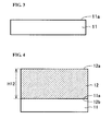
- FIG. 3 is a sectional view schematically showing a support substrate in the embodiment of the present invention.
- a support substrate 11 composed of Al a Ga (1-a) N (0 ⁇ a ⁇ 1) is prepared (Step S1).
- the composition ratio a of Al in the support substrate 11 prepared in Step S1 is larger than the composition ratio b of Al in an AlGaN bulk crystal 12 to be grown in Step S2 described below.
- the composition ratios a and b of Al in the support substrate 11 and the AlGaN bulk crystal 12 are molar ratios of Al.
- the decomposition temperature of a crystal constituting the support substrate 11 increases as the composition ratio a of Al in the support substrate 11 increases. Therefore, even when an AlGaN bulk crystal is grown at a high temperature in Step S2 described below, decomposition of the support substrate 11 can be suppressed, and thus an AlGaN bulk crystal having a large thickness can be grown.
- the composition ratio a of Al in the support substrate 11 is preferably as large as possible, and for example, the composition ratio a is preferably 0.8 or more and more preferably 1.
- the support substrate 11 having a primary surface 11a with a size of, for example, 2 inches or more in diameter is preferably prepared. Consequently, an AlGaN bulk crystal with a large diameter can be grown.
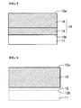
- FIG 4 is a sectional view schematically showing a state in which an AlGaN bulk crystal is grown according to the embodiment of the present invention.
- the AlGaN bulk crystal 12 having a primary surface 12a and composed of Al b Ga (1-b) N (0 ⁇ b ⁇ 1) is grown on the support substrate 11 (Step S2).
- the composition ratio b of Al in the AlGaN bulk crystal 12 grown in Step S2 is smaller than the composition ratio a of Al in the support substrate 11 prepared in Step S1. Namely, a relation of a > b is established between the composition ratio a of Al in the support substrate 11 and the composition ratio b of Al in the AlGaN bulk crystal 12.
- a relation of a > b > 0.5a, more preferably a relation of 0.7a ⁇ b ⁇ 0.125a, is established between the composition ratio a of Al in the support substrate 11 and the composition ratio b of Al in the AlGaN bulk crystal 12.
- decomposition of the support substrate 11 can be further suppressed, and the high-quality AlGaN bulk crystal 12 can be grown.
- Step S2 the AlGaN bulk crystal 12 is grown at a high temperature which can suppress the formation of irregularity in the growth surface (primary surface 12a). Even when the AlGaN bulk crystal 12 is grown at a high temperature, decomposition of the support substrate 11 can be suppressed because the support substrate 11 has a high composition ratio a of Al according to the embodiment. Therefore, the formation of irregularity in the growth surface can be suppressed, and the AlGaN bulk crystal 12 having a large thickness can be grown.
- the growth temperature of the AlGaN bulk crystal 12 is preferably 1650°C or more and more preferably 1650°C or more and 1800°C or less.
- the temperature is 1650°C or more
- the primary surface 12a of the AlGaN bulk crystal 12, which is the growth surface can be made very flat.
- the temperature is 1800°C or less, decomposition of the support substrate 11 can be effectively suppressed, thereby increasing the thickness H12.
- the growth temperature represents, for example, the temperature of the support substrate 11.
- the AIGaN bulk crystal 12 having a large thickness H12 which is preferably 1 mm or more, more preferably 2 mm or more, and still more preferably 4 mm or more can be grown.
- the thickness H12 there is no upper limit of the thickness H12, in the embodiment, the AlGaN bulk crystal 12 having a thickness H12 of, for example, 50 mm or less can be easily manufactured.
- Step S2 the composition ratio b of Al in the AlGaN bulk crystal 12 is smaller than the composition ratio a of Al in the support substrate 11.
- tensile stress is applied so that the support substrate 11 having a relatively small lattice constant is matched with the AlGaN bulk crystal 12 having a relatively large lattice constant. Therefore, it is possible to suppress tensile stress from being applied to the AlGaN bulk crystal 12, thereby suppressing the occurrence of cracks, defects, dislocation, and the like in the AlGaN bulk crystal 12. Therefore, crystallinity of the AlGaN bulk crystal 12 can be improved.
- the dislocation density which is an index for crystallinity of the AlGaN bulk crystal 12 is preferably 1 ⁇ 10 8 cm -2 or less, more preferably 1 ⁇ 10 7 cm -2 or less, still more preferably 1 ⁇ 10 6 cm -2 or less, and most preferably 5 ⁇ 10 5 cm -2 or less.
- the composition ratio b of Al in the AlGaN bulk crystal 12 is smaller than the composition ratio a of Al in the support substrate 11, and thus the AlGaN bulk crystal 12 having such a dislocation density can be grown.
- the composition ratio b of the AlGaN bulk crystal 12 is not limited to being constant, but the composition ratio b may monotonically decrease toward the growth surface.
- the expression “monotonically decrease” represents that the composition ratio b is always constant or decreases from the back side 12b on the support substrate 11 side to the primary surface 12a which is the growth surface (in the growth direction), and the composition ratio b of the primary surface 12a is lower than that of the back side 12b. Namely, the expression “monotonically decrease” does not include the case in which the composition b increases in the growth direction.
- the AlGaN bulk crystal 12 is grown preferably at a growth rate of 30 ⁇ m/hr or more, more preferably 100 ⁇ m/hr or more and 180 ⁇ m/hr or less. Since the AlGaN bulk crystal 12 can be grown at a high temperature as described above, the growth rate can be increased to such a value. Therefore, the AlGaN bulk crystal 12 can be manufactured with a high manufacturing efficiency.
- the AlGaN bulk crystal 12 is preferably grown so that the primary surface 12a is any one of the c-plane, the a-plane, and the m-plane, In this case, a high-performance semiconductor element can be manufactured using the AIGaN bulk crystal 12.
- the method for growing the AlGaN bulk crystal 12 is not particularly limited, and a vapor phase growth method such as a sublimation growth method, a HVPE (Hydride Vapor Phase Epitaxy) method, a MBE (Molecular Beam Epitaxy) method, or a MOCVD (Metal Organic Chemical Vapor Deposition) method, a liquid phase method such as a flux growth method, a high-nitrogen pressure solution growth method, or the like can be used.
- the sublimation growth method is preferably used from the viewpoint that growth can be performed at a very high temperature.
- FIG. 5 is a sectional view schematically showing a state in which another AlGaN bulk crystal is grown in the embodiment of the present invention.
- growth Step S2 may include a step of growing a first layer 13 in which a group III element is diffused on the support substrate 11, and a step of growing a second layer 14 composed of Al b Ga (1-b) N on the first layer 13.
- the first layer 13 contains a large amount of Al
- the second layer 14 contains a large amount of Ga.
- the Al amount is relatively large on the support substrate side
- the Ga amount is relatively large on the interface side with the second layer 14.
- the interface between the first and second layers 13 and 14 can be measured by, for example, SIMS (Secondary Ion Mass Spectrometry).
- the AlGaN bulk crystal 12 When the AlGaN bulk crystal 12 is grown at a high temperature, a group III element (Al element or Al element and Ga element) constituting the support substrate 11 diffuses, and thus the first layer 13 disposed on the support substrate 11 side in the AlGaN bulk crystal 12 contains the group III element. Namely, when the AlGaN bulk crystal 12 is grown at a high temperature, the first layer 13 is formed. By forming the first layer 13, the occurrence of irregularity in the growth surface of the second layer 14 can be more effectively suppressed.
- the growth temperature is for example 1650°C or more. The growth at such a high temperature can further improve quality of the primary surface 12a side of the AlGaN bulk crystal 12.
- the AlGaN bulk crystal 12 may include three or more layers.
- FIG. 6 is a sectional view schematically showing a state in which a support substrate is removed in this embodiment of the present invention.
- Step S3 may not be performed.
- the removal method is not particularly limited, but, for example, a method such as cutting, cleavage, or the like can be used.
- the AlGaN bulk crystal 12 (in this embodiment, the AlGaN bulk crystal 10) is cut out from a laminate of the support substrate 11 and the AlGaN bulk crystal 12.
- the support substrate 11 may be removed from the laminate of the support substrate 11 and the AlGaN bulk crystal 12 or a portion including the interface (back side 12b) between the AlGaN bulk crystal 12 and the support substrate 11 in the AlGaN bulk crystal 12 may be further removed.
- the AlGaN bulk crystal 12 can be easily separated because it is composed of a single crystal.
- Cutting includes mechanically removing at least the support substrate 11 with a slicer having an outer cutting edge of an electroplated diamond wheel.
- Cleavage includes removing at least the support substrate 11 along a crystal lattice plane.
- the AlGaN bulk crystal 10 is preferably cut out so that the primary surface 10a is any one of the c-plane, the a-plane, and the m-plane.
- the AlGaN bulk crystal 12 is grown so that the primary surface 10a is any one of the c-plane, the a-plane, and the m-plane
- the AlGaN bulk crystal 10 having the primary surface 10a with the same plane orientation as the AlGaN bulk crystal 12 can be manufactured by cutting out the AlGaN bulk crystal 12 in parallel with the primary surface 12a of the crystal 12.
- the AlGaN bulk crystal 10 shown in Fig. 1 can be manufactured by performing Steps S1 to S3.
- the composition ratio a of Al in the support substrate 11 is larger than the composition ratio b of Al in the AlGaN bulk crystal 12.
- the method for manufacturing the AlGaN bulk crystal 10 or 12 according to the embodiment is capable of suppressing decomposition of the support substrate 11 even when the AlGaN bulk crystal 12 is grown at a high temperature. Therefore, the manufacturing method of the present invention is capable of suppressing the formation of irregularity in the growth surface and manufacturing the AlGaN bulk crystal 10 or 12 having large thickness H10 or H12.
- a lattice constant increases as the composition ratio of Al decreases. Therefore, in a laminate of the support substrate 11 and the AlGaN bulk crystal 12, tensile stress is suppressed from being applied to the AlGaN bulk crystal 12 having a relatively large lattice constant. As a result, introduction of cracks, defects, and the like in the AlGaN bulk crystal 12 can be suppressed, and thus the high-quality AlGaN bulk crystal 10 or 12 can be manufactured.
- Al 2 O 3 , Ga 2 O 3 (gallium oxide), and the like contained in raw materials or produced from the raw materials are incorporated into the AlGaN bulk crystal 12.
- a pit or the like is formed in the AlGaN bulk crystal 10 or 12, thereby often producing polycrystals.
- the crystal 12 is generally grown at a high temperature.
- the growth of the crystal 12 at a high temperature causes decomposition of Al 2 O 3 , Ga 2 O 3 , and the like, and thus Al 2 O 3 , Ga 2 O 3 , and the like can be suppressed from being directly incorporated into the AlGaN bulk crystal 12. As a result, the formation of polycrystals can be suppressed, and the high-quality AlGaN bulk crystal 10 or 12 can be manufactured.
- the composition ratio a of Al in the support substrate 11 is larger than the composition ratio b of Al in the AlGaN bulk crystal 12, the high-quality AlGaN bulk crystal 10 or 12 having a large thickness H10 or H12 can be stably manufactured with high reproducibility.
- Figure 7 is a sectional view schematically showing an AlGaN substrate according to an embodiment of the present invention. An AlGaN substrate according to this embodiment is described with reference to Fig. 7 .
- an AlGaN substrate 20 according to this embodiment is formed using the AlGaN bulk crystal 10 or 12 according to Embodiment 1. Namely, the AlGaN substrate 20 is composed of Al b Ga (1-b) N (0 ⁇ b ⁇ 1).
- the AlGaN substrate 20 has a primary surface 20a, and the primary surface 20a is preferably any one of the c-plane, the a-plane, and the m-plane.
- Figure 8 is a flow chart showing an AlGaN substrate manufacturing method according to the embodiment. Next, the AlGaN substrate manufacturing method according to the embodiment is described with reference to Fig. 8 .
- the AlGaN bulk crystal 10 or 12 is manufactured by the AlGaN bulk crystal manufacturing method according to Embodiment 1 (Steps S1 to S3). Steps S1 to S3 are substantially the same as in Embodiment 1, and thus a description thereof is not repeated.
- FIG 9 is a sectional view schematically showing a state in which an AlGaN substrate is cut out from an AlGaN bulk crystal according to this embodiment.
- an AlGaN substrate 20 is cut out from the AlGaN bulk crystal 10 or 12 (Step S4).
- the AlGaN substrate 20 cut out in Step S4 is composed of Al b Ga (1-b) N (0 ⁇ b ⁇ 1).
- one AlGaN substrate 20 may be cut out, but a plurality of AlGaN substrates 20 are preferably cut out. Since the AlGaN bulk crystal 10 or 12 having a large thickness H10 or H12 is manufactured in Embodiment 1, a plurality of AlGaN substrates 20 can be easily cut out.
- a cutout method is not particularly limited, but the AlGaN substrate 20 can be separated from the AlGaN bulk crystal 10 or 12 by cutting or cleavage.
- the AlGaN substrate 20 shown in Fig. 7 can be manufactured by performing Steps S1 to S4.
- At least one AlGaN substrate 20 can be cut out from the bulk crystal 10 or 12 of Embodiment 1 (Step S4).
- the high-quality AlGaN substrate 20 can be manufactured because the AlGaN bulk crystal 10 or 20 has high quality.
- the AlGaN bulk crystal 10 or 20 has a large thickness H10 or H12, a plurality of AlGaN substrates 20 can be cut out from the AlGaN bulk crystal 10 or 20 of Embodiment 1. In this case, the manufacturing cost per AlGaN substrate 20 can be decreased.
- the AlGaN substrate 20 manufactured according to this embodiment can be preferably used as substrates for light-emitting elements such as a light-emitting diode, a laser diode, and the like; electronic elements such as a rectifier, a bipolar transistor, a field-effect transistor, HEMT (High Electron Mobility Transistor), and the like; semiconductor sensors such as a temperature sensor, a pressure sensor, a radiation sensor, a visible-ultraviolet sensor, and the like; and devices such as a SAW device (Surface Acoustic Wave Device), a vibrator, a resonator, an oscillator, a MEMS (Micro Electro Mechanical System) part, a piezoelectric actuator, and the like.
- light-emitting elements such as a light-emitting diode, a laser diode, and the like
- electronic elements such as a rectifier, a bipolar transistor, a field-effect transistor, HEMT (High Electron Mobility Transistor), and the like
- AlGaN bulk crystals of Examples 1 to 4 were manufactured according to the above-described AlGaN bulk crystal manufacturing method of Embodiment 1.
- a support substrate composed of Al a Ga (1-a) N (0 ⁇ a ⁇ 1) was prepared (Step S1).
- the composition ratio a of Al was as shown in Table I below.
- a primary surface of the support substrate was the c-plane.
- a bulk crystal composed of Al b Ga (1-b) N (0 ⁇ b ⁇ 1) and having a primary surface was grown on the support substrate (Step S2).
- the composition ratio b of Al in the bulk crystal was smaller than the composition ratio a of Al in the support substrate.
- the composition ratio b of the primary surface, the growth method, and the growth temperature of the bulk crystal were as shown in Table I below.
- the primary surface of the bulk crystal was the c-plane.
- the Al b Ga (1-b) N bulk crystal manufacturing method basically had the same configuration as for the Al b Ga (1-b) N bulk crystals of Examples 1 to 4 and Comparative Examples 1 and 2 but was different in that a support substrate with the m-plane as the primary surface was used, and a bulk crystal was manufactured so that the primary surface was the m-plane.
- the Al b Ga (1-b) N bulk crystal manufacturing method basically had the same configuration as for the Al b Ga (1-b) N bulk crystals of Examples 1 to 4 and Comparative Examples 1 and 2 but was different in that a support substrate with the a-plane as the primary surface was used, and a bulk crystal was manufactured so that the primary surface was the a-plane.
- the thickness was measured in a recessed portion (i.e., a portion with the smallest thickness) of the growth surface (primary surface) from the interface (back side) with the support substrate.
- the growth rate was calculated from a time required for growing the AlGaN bulk crystal with each of the thicknesses.
- Fig. 10 is a sectional view illustrating the method for confirming the first layer.
- the dislocation density was measured as follows: First, each of the AlGaN bulk crystals was etched by immersing for 30 minutes in a melt prepared by melting KOH and NaOH (sodium hydroxide) at a ratio of 1:1 in a platinum crucible at 250°C. Then, each of the AlGaN bulk crystals was washed, and the number of etch pits per unit area in the surface was counted with a microscope.
- the dislocation density measured as described above the dislocation density of 1 ⁇ 10 4 cm -2 or more and 5 ⁇ 10 5 cm -2 or less was evaluated as A, the dislocation density of over 5 ⁇ 10 5 cm -2 and 1 ⁇ 10 7 cm -2 or less was evaluated as B, the dislocation density of over 1 ⁇ 10 7 cm -2 and 1 ⁇ 10 8 cm -2 or less was evaluated as C, the dislocation density of over 1 ⁇ 10 8 cm -2 was evaluated as D, and unmeasurable dislocation density was evaluated as E.
- Tables I to III indicate that in Examples 1 to 12 in which the composition ratio a of Al in the support substrate was larger than the composition ratio b of Al in the AlGaN bulk crystal, the AlGaN bulk crystals have a large thickness of 1 mm or more and a low dislocation density of 1 ⁇ 10 8 cm -2 or less. Therefore, it is found that in Examples 1 to 12, AlGaN bulk crystals of high quality having a large thickness can be grown. In addition, in Examples 1 to 12, since the bulk crystals are grown at a high temperature, the bulk crystals can be grown at a high growth rate of 30 ⁇ m/hr or more. In Examples 1 to 3, 5 to 7, and 9 to 11, a first layer in which at least one of Al element and Ga element as group III elements is diffused is formed.
- the support substrate was composed of AlN
- Al 0.7 Ga 0.3 N bulk crystals can be grown by a sublimation growth method at a high temperature of 1800°C. Therefore, the AlGaN bulk crystal of Example 1 has a low dislocation density of 1 ⁇ 10 4 cm -2 or more and 5 ⁇ 10 5 cm -2 or less. Further, a bulk crystal having a large thickness of 4 mm can be grown in spite of being grown at a high temperature.
- Comparative Examples 1 to 6 in which an Al 0.5 Ga 0.5 N bulk crystal (Al composition ratio b of 0.5) was grown on a support substrate (Al composition ratio a of 0) composed of GaN, the composition ratio a of Al in the support substrate is smaller than the composition ratio b of Al in the bulk crystal. Therefore, in Comparative Examples 1, 3, and 5 in which a bulk crystal was grown at a low temperature of 1000°C in order to suppress decomposition of the support substrate, large irregularity occurs in the surface, and the thickness of a recessed portion in the primary surface, which is a substantial thickness, is as small as 0.2 mm.
- a lattice constant of the bulk crystal is smaller than a lattice constant of the support substrate, and thus tensile stress is applied to the bulk crystal, thereby causing a high dislocation density of over 1 ⁇ 10 8 cm -2 . Further, the growth rate is low because of the low growth temperature.
- composition ratio a of Al in the support substrate is larger than the composition ratio b of Al in the bulk crystal, a high-quality AlGaN bulk crystal having a large thickness can be manufactured. Also it was confirmed that an AlGaN bulk crystal can be manufactured so that the primary surface is any one of the c-plane, the a-plane, and the m-plane.
- the support substrate was removed from each of the AlGaN bulk crystals after growth by slicing with a wire saw to produce an AlGaN bulk crystal.
- Comparative Examples 1, 3, and 5 a plurality of AlGaN substrates could not be cut out because of the small thickness.
- the support substrate could not be removed because the AlGaN bulk crystal could not be grown, and thus an AlGaN substrate could not be manufactured.
- composition ratio a of Al in the support substrate is larger than the composition ratio b of Al in the bulk crystal, a high-quality AlGaN bulk crystal having a large thickness without having a support substrate can be manufactured. Also it was confirmed that when the composition ratio a of Al in the support substrate is larger than the composition ratio b of Al in the bulk crystal, an AlGaN bulk crystal having a large thickness can be manufactured, and thus a plurality of AlGaN substrates can be cut out from the AlGaN bulk crystal.
Landscapes
- Chemical & Material Sciences (AREA)
- Engineering & Computer Science (AREA)
- Crystallography & Structural Chemistry (AREA)
- Materials Engineering (AREA)
- Metallurgy (AREA)
- Organic Chemistry (AREA)
- Chemical Kinetics & Catalysis (AREA)
- General Chemical & Material Sciences (AREA)
- Inorganic Chemistry (AREA)
- Crystals, And After-Treatments Of Crystals (AREA)
Abstract
Description
- The present invention relates to an AlGaN bulk crystal manufacturing method and an AlGaN substrate manufacturing method.
- AlxGa(1-x)N (0 < x < 1) (also referred to as "AlGaN") crystals are very useful as materials for forming light-emitting elements, electronic elements, and semiconductor devices such as semiconductor sensors.
- Examples of methods for growing such AlGaN crystals include a method for growing by spontaneous nucleation without using a support substrate and a method for growing using a support substrate. It is difficult to stably grow large AlGaN crystals by the method for growing by spontaneous nucleation.
- The method for growing an AlGaN crystal using a support substrate is disclosed in, for example, Japanese Unexamined Patent Application Publication No.
2004-331453 Patent Literature 1 discloses that silicon (Si), sapphire (Al2O3), SiC (silicon carbide), ZrB2 (zirconium boride), or a group III-V compound is used for the support substrate. - PTL 1: Japanese Unexamined Patent Application Publication No.
2004-331453 - However, the inventors have found that growth of an AlGaN crystal using a support substrate as in
Patent Literature 1 has the problems below. - That is, the inventors have found that growth of an AlGaN crystal at a low temperature has the problem of deteriorating the quality of the AlGaN crystal. Specific forms of the deterioration include the presence of crystal defects such as dislocation or the like at a high density in the AlGaN crystal, the nonuniform AlGaN crystal due to the formation of large irregularity on a growth surface, and the like.
- The inventors have found that when an AlGaN crystal is grown at a high temperature (e.g., 1200°C or more) in order to improve the quality of the AlGaN crystal, an AlGaN crystal having a large thickness cannot be grown due to vaporization and decomposition of the AlGaN crystal from the back side of the support substrate. When the AlGaN crystal has a small thickness, an AlGaN substrate cannot be cut out from the AlGaN crystal. Only a small number of AlGaN substrates can be cut out.
- The present invention has been achieved in consideration of the above problems, and an object of the invention is to provide an AlGaN bulk crystal manufacturing method for manufacturing an AlGaN bulk crystal of high quality.
- Another object of the invention is to provide an AlGaN substrate manufacturing method for manufacturing an AlGaN substrate of high quality.
- An AlGaN bulk crystal manufacturing method of the present invention includes the following steps: First, a support substrate composed of AlaGa(1-a)N (0 < a ≤ 1) is prepared. Then, a bulk crystal composed of AlbGa(1-b)N (0 < b< 1) with a primary surface is grown on the support substrate. The composition ratio a of Al in the support substrate is larger than the composition ratio b of Al in the bulk crystal.
- As a result of intensive research, the inventors have found that the decomposition temperature of a crystal increases as the Al composition ratio of a crystal increases. In the present invention, therefore, the composition ratio a of Al in AlaGa(1-a)N (0 < a ≤ 1) of the support substrate is larger than the composition ratio b of Al in AlbGa(1-b)N (0 < b< 1) of the bulk crystal. Therefore, even when a bulk crystal is grown at a temperature required for growing a bulk crystal in which formation of irregularity is suppressed, vaporization and decomposition of the support substrate can be suppressed. Thus, a bulk crystal can be grown at a high temperature for a long time. Therefore, it is possible to grow a bulk crystal having a large thickness while suppressing formation of irregularity in a growth surface.
- In addition, the composition ratio b of Al in the bulk crystal is smaller than the composition ratio a of Al in the support substrate. As the Al composition ratio decreases, a lattice constant increases. In a laminate of the support substrate and the bulk crystal, tensile stress is applied to the support substrate having a relatively small lattice constant so as to match with the bulk crystal having a relatively large lattice constant. Therefore, it is possible to suppress tensile stress from being applied to the bulk crystal, thereby suppressing the occurrence of cracks, defects, dislocation, and the like. Consequently, the crystallinity of the bulk crystal can be improved.
- As described above, when the composition ratio a of Al in the support substrate is larger than the composition ratio b of Al in the bulk crystal, an AlGaN bulk crystal of high quality having a large thickness can be manufactured.
- In the above-described AlGaN bulk crystal manufacturing method, a bulk crystal having a thickness of 1 mm or more is preferably grown in the growth step.
- According to the AlGaN bulk crystal manufacturing method of the present invention, decomposition of the support substrate can be suppressed, and thus an AlGaN bulk crystal having a thickness of as large as 1 mm or more can be manufactured.
- In the above-described AlGaN bulk crystal manufacturing method, the growth step preferably includes a step of growing a first layer containing a group III element diffused therein on the support substrate, and a step of growing a second layer composed of AlbGa(1-b)N on the first layer.
- When a bulk crystal is grown at a high temperature, a group III element constituting a support substrate diffuses into the bulk crystal. Therefore, the first layer disposed on the support substrate side in the bulk crystal contains the group III element. That is, the formation of the first layer corresponds to the growth of the bulk crystal at a high temperature. The formation of the first layer can effectively suppress the occurrence of irregularity in the second layer growth surface. Therefore, the quality of the bulk crystal can be further improved.
- In the above-described AlGaN bulk crystal manufacturing method, in the growth step, the bulk crystal is preferably grown so that the Al concentration decreases from the support substrate side to the primary surface.
- Therefore, tensile stress applied to the growth surface can be further suppressed. As a result, the AlGaN crystal of higher quality can be manufactured on the growth surface.
- In the above-described AlGaN bulk crystal manufacturing method, in the growth step, the bulk crystal is preferably grown at 1650°C or more.
- In the present invention, decomposition of the support substrate can be suppressed even in growth at a high temperature of 1650°C or more. Therefore, the formation of irregularity in the growth surface can be further suppressed.
- In the above-described AlGaN bulk crystal manufacturing method, in the growth step, the bulk crystal is preferably grown so that the primary surface is any one of a c-plane, an a-plane, and an m-plane. In this case, a high-performance semiconductor element can be manufactured using the bulk crystal.
- The above-described AlGaN bulk crystal manufacturing method, after the growth step, preferably further includes a step of removing at least the support substrate. As a result, a bulk crystal from which the support substrate is removed can be manufactured.
- An AlGaN substrate manufacturing method of the present invention includes a step of manufacturing an AlGaN bulk crystal by the above-described AlGaN bulk crystal manufacturing method, and a step of cutting out at least one AlbGa(1-b)N substrate from the bulk crystal.
- According to the AlGaN substrate manufacturing method of the present invention, an AlGaN crystal of high quality with a large thickness which is manufactured by the AlGaN bulk crystal manufacturing method of the present invention is used. Therefore, an AlGaN substrate of high quality can be manufactured.
- According to an AlGaN bulk crystal manufacturing method of the present invention, a support substrate having an Al composition ratio a larger than an Al composition ratio b of a bulk crystal is used, and thus an AlGaN bulk crystal of high quality having a large thickness can be manufactured.
- According to an AlGaN substrate manufacturing method of the present invention, an AlGaN substrate of high quality can be manufactured using the AlGaN bulk crystal. Brief Description of Drawings
-
- [
Fig. 1] Fig. 1 is a sectional view schematically showing an AlGaN bulk crystal inEmbodiment 1 of the present invention. - [
Fig. 2] Fig. 2 is a flow chart showing an AlGaN bulk crystal manufacturing method inEmbodiment 1 of the present invention. - [
Fig. 3] Fig. 3 is a sectional view schematically showing a support substrate inEmbodiment 1 of the present invention. - [
Fig. 4] Fig. 4 is a sectional view schematically showing a state in which an AlGaN bulk crystal is grown inEmbodiment 1 of the present invention. - [
Fig. 5] Fig. 5 is a sectional view schematically showing a state in which another AlGaN bulk crystal is grown inEmbodiment 1 of the present invention. - [
Fig. 6] Fig. 6 is a sectional view schematically showing a state in which a support substrate is removed inEmbodiment 1 of the present invention. - [
Fig. 7] Fig. 7 is a sectional view schematically showing an AlGaN substrate in Embodiment 2 of the present invention. - [
Fig. 8] Fig. 8 is a flow chart showing an AlGaN substrate manufacturing method in Embodiment 2 of the present invention. - [
Fig. 9] Fig. 9 is a sectional view schematically showing a state in which an AlGaN substrate is cut out from an AlGaN bulk crystal in Embodiment 2 of the present invention. - [
Fig. 10] Fig. 10 is a sectional view illustrating a method for confirming the presence of a first layer in an example. - Embodiments of the present invention are described below based on the drawings. In the drawings, the same portion or corresponding portions are denoted by the same reference numeral, and a description thereof is not repeated.
-
Figure 1 is a sectional view schematically showing an AlGaN bulk crystal according to an embodiment of the present invention. AnAlGaN bulk crystal 10 according to this embodiment is described with reference toFig. 1 . - The
AlGaN bulk crystal 10 according to the embodiment is AlbGa(1-b)N (0 < b < 1). TheAlGaN bulk crystal 10 has aprimary surface 10a. Theprimary surface 10a is preferably, for example, any one of a {1000} plane (c-plane), a {11-20} plane (a-plane), and a {1-100} plane (m-plane). From a crystallographic viewpoint, brackets {} represent a family of planes, and a negative index is shown by placing "-" (bar) above a number, but in this specification, a negative index is shown by placing a minus sign before a number. - The
AlGaN bulk crystal 10 preferably has a dislocation density of 1 × 108 cm-2 or less, more preferably 1 × 107 cm-2 or less, still more preferably 1 × 106 cm-2 or less, and most preferably 5 × 105 cm-2 or less. In this case, when a device is manufactured using anAlGaN substrate 20 formed from the AlGaN bulk crystal, characteristics of the device can be improved. A dislocation density can be measured by, for example, a method of counting a number of pits produced by etching in molten KOH (potassium hydroxide) and dividing the number by a unit area. - The
AlGaN bulk crystal 10 preferably has a thickness H10 of 1 mm or more, more preferably 2 mm or more, and still more preferably 4 mm or more. With a thickness of 1 mm or more, a larger number of AlGaN substrates can be manufactured from theAlGaN bulk crystal 10, thereby decreasing the cost required for manufacturing an AlGaN substrate. In addition, defects such as dislocation can be decreased by thickening theAlGaN bulk crystal 10, and thus a high-quality AlGaN crystal 10 can be formed. -
Figure 2 is a flow chart showing an AlGaN bulk crystal manufacturing method according to the embodiment of the present invention. The AlGaN bulk crystal manufacturing method according to the embodiment of the present invention is described with reference toFig. 2 . -
Figure 3 is a sectional view schematically showing a support substrate in the embodiment of the present invention. As shown inFigs. 2 and3 , first, asupport substrate 11 composed of AlaGa(1-a)N (0 < a ≤ 1) is prepared (Step S1). The composition ratio a of Al in thesupport substrate 11 prepared in Step S1 is larger than the composition ratio b of Al in anAlGaN bulk crystal 12 to be grown in Step S2 described below. The composition ratios a and b of Al in thesupport substrate 11 and theAlGaN bulk crystal 12 are molar ratios of Al. - The decomposition temperature of a crystal constituting the
support substrate 11 increases as the composition ratio a of Al in thesupport substrate 11 increases. Therefore, even when an AlGaN bulk crystal is grown at a high temperature in Step S2 described below, decomposition of thesupport substrate 11 can be suppressed, and thus an AlGaN bulk crystal having a large thickness can be grown. From the viewpoint of resistance to vaporization and decomposition, the composition ratio a of Al in thesupport substrate 11 is preferably as large as possible, and for example, the composition ratio a is preferably 0.8 or more and more preferably 1. - In Step S1, the
support substrate 11 having aprimary surface 11a with a size of, for example, 2 inches or more in diameter is preferably prepared. Consequently, an AlGaN bulk crystal with a large diameter can be grown. -
Figure 4 is a sectional view schematically showing a state in which an AlGaN bulk crystal is grown according to the embodiment of the present invention. Next, as shown inFigs. 2 and4 , theAlGaN bulk crystal 12 having aprimary surface 12a and composed of AlbGa(1-b)N (0 < b < 1) is grown on the support substrate 11 (Step S2). The composition ratio b of Al in theAlGaN bulk crystal 12 grown in Step S2 is smaller than the composition ratio a of Al in thesupport substrate 11 prepared in Step S1. Namely, a relation of a > b is established between the composition ratio a of Al in thesupport substrate 11 and the composition ratio b of Al in theAlGaN bulk crystal 12. Preferably a relation of a > b > 0.5a, more preferably a relation of 0.7a ≥ b ≥ 0.125a, is established between the composition ratio a of Al in thesupport substrate 11 and the composition ratio b of Al in theAlGaN bulk crystal 12. In this case, decomposition of thesupport substrate 11 can be further suppressed, and the high-qualityAlGaN bulk crystal 12 can be grown. - In Step S2, the
AlGaN bulk crystal 12 is grown at a high temperature which can suppress the formation of irregularity in the growth surface (primary surface 12a). Even when theAlGaN bulk crystal 12 is grown at a high temperature, decomposition of thesupport substrate 11 can be suppressed because thesupport substrate 11 has a high composition ratio a of Al according to the embodiment. Therefore, the formation of irregularity in the growth surface can be suppressed, and theAlGaN bulk crystal 12 having a large thickness can be grown. - Specifically, the growth temperature of the
AlGaN bulk crystal 12 is preferably 1650°C or more and more preferably 1650°C or more and 1800°C or less. When the temperature is 1650°C or more, theprimary surface 12a of theAlGaN bulk crystal 12, which is the growth surface, can be made very flat. When the temperature is 1800°C or less, decomposition of thesupport substrate 11 can be effectively suppressed, thereby increasing the thickness H12. The growth temperature represents, for example, the temperature of thesupport substrate 11. - In addition, the
AIGaN bulk crystal 12 having a large thickness H12 which is preferably 1 mm or more, more preferably 2 mm or more, and still more preferably 4 mm or more can be grown. Although there is no upper limit of the thickness H12, in the embodiment, theAlGaN bulk crystal 12 having a thickness H12 of, for example, 50 mm or less can be easily manufactured. - As the composition ratios a and b of Al decrease, a lattice constant increases. In Step S2, the composition ratio b of Al in the
AlGaN bulk crystal 12 is smaller than the composition ratio a of Al in thesupport substrate 11. In a laminate of thesupport substrate 11 and theAlGaN bulk crystal 12, tensile stress is applied so that thesupport substrate 11 having a relatively small lattice constant is matched with theAlGaN bulk crystal 12 having a relatively large lattice constant. Therefore, it is possible to suppress tensile stress from being applied to theAlGaN bulk crystal 12, thereby suppressing the occurrence of cracks, defects, dislocation, and the like in theAlGaN bulk crystal 12. Therefore, crystallinity of theAlGaN bulk crystal 12 can be improved. - The dislocation density which is an index for crystallinity of the
AlGaN bulk crystal 12 is preferably 1 × 108 cm-2 or less, more preferably 1 × 107 cm-2 or less, still more preferably 1 × 106 cm-2 or less, and most preferably 5 × 105 cm-2 or less. In the embodiment, the composition ratio b of Al in theAlGaN bulk crystal 12 is smaller than the composition ratio a of Al in thesupport substrate 11, and thus theAlGaN bulk crystal 12 having such a dislocation density can be grown. - When the
AlGaN bulk crystal 12 is grown so that the Al concentration decreases from thesupport substrate 11 side (backside 12b) to the growth surface (primary surface 12a), tensile stress applied to the growth surface can be further suppressed, and consequently the dislocation density can be further decreased. That is, the composition ratio b of theAlGaN bulk crystal 12 is not limited to being constant, but the composition ratio b may monotonically decrease toward the growth surface. The expression "monotonically decrease" represents that the composition ratio b is always constant or decreases from theback side 12b on thesupport substrate 11 side to theprimary surface 12a which is the growth surface (in the growth direction), and the composition ratio b of theprimary surface 12a is lower than that of theback side 12b. Namely, the expression "monotonically decrease" does not include the case in which the composition b increases in the growth direction. - In Step S2, the
AlGaN bulk crystal 12 is grown preferably at a growth rate of 30 µm/hr or more, more preferably 100 µm/hr or more and 180 µm/hr or less. Since theAlGaN bulk crystal 12 can be grown at a high temperature as described above, the growth rate can be increased to such a value. Therefore, theAlGaN bulk crystal 12 can be manufactured with a high manufacturing efficiency. - In Step S2, the
AlGaN bulk crystal 12 is preferably grown so that theprimary surface 12a is any one of the c-plane, the a-plane, and the m-plane, In this case, a high-performance semiconductor element can be manufactured using theAIGaN bulk crystal 12. - The method for growing the
AlGaN bulk crystal 12 is not particularly limited, and a vapor phase growth method such as a sublimation growth method, a HVPE (Hydride Vapor Phase Epitaxy) method, a MBE (Molecular Beam Epitaxy) method, or a MOCVD (Metal Organic Chemical Vapor Deposition) method, a liquid phase method such as a flux growth method, a high-nitrogen pressure solution growth method, or the like can be used. In Step S2, the sublimation growth method is preferably used from the viewpoint that growth can be performed at a very high temperature. -
Figure 5 is a sectional view schematically showing a state in which another AlGaN bulk crystal is grown in the embodiment of the present invention. As shown inFig. 5 , growth Step S2 may include a step of growing afirst layer 13 in which a group III element is diffused on thesupport substrate 11, and a step of growing asecond layer 14 composed of AlbGa(1-b)N on thefirst layer 13. In detail, in theAlGaN bulk crystal 12, thefirst layer 13 contains a large amount of Al, and thesecond layer 14 contains a large amount of Ga. In thefirst layer 13, the Al amount is relatively large on the support substrate side, and the Ga amount is relatively large on the interface side with thesecond layer 14. The interface between the first andsecond layers - When the
AlGaN bulk crystal 12 is grown at a high temperature, a group III element (Al element or Al element and Ga element) constituting thesupport substrate 11 diffuses, and thus thefirst layer 13 disposed on thesupport substrate 11 side in theAlGaN bulk crystal 12 contains the group III element. Namely, when theAlGaN bulk crystal 12 is grown at a high temperature, thefirst layer 13 is formed. By forming thefirst layer 13, the occurrence of irregularity in the growth surface of thesecond layer 14 can be more effectively suppressed. The growth temperature is for example 1650°C or more. The growth at such a high temperature can further improve quality of theprimary surface 12a side of theAlGaN bulk crystal 12. - Although the case in which the
AlGaN bulk crystal 12 includes two layers is described by giving an example with reference toFig. 5 , theAlGaN bulk crystal 12 may include three or more layers. -
Figure 6 is a sectional view schematically showing a state in which a support substrate is removed in this embodiment of the present invention. Next, as shown inFigs. 2 and6 , at least thesupport substrate 11 is removed (Step S3). Step S3 may not be performed. - The removal method is not particularly limited, but, for example, a method such as cutting, cleavage, or the like can be used. In the removal, the AlGaN bulk crystal 12 (in this embodiment, the AlGaN bulk crystal 10) is cut out from a laminate of the
support substrate 11 and theAlGaN bulk crystal 12. In this case, only thesupport substrate 11 may be removed from the laminate of thesupport substrate 11 and theAlGaN bulk crystal 12 or a portion including the interface (backside 12b) between theAlGaN bulk crystal 12 and thesupport substrate 11 in theAlGaN bulk crystal 12 may be further removed. When a portion including theback side 12b is further removed, theAlGaN bulk crystal 12 can be easily separated because it is composed of a single crystal. - Cutting includes mechanically removing at least the
support substrate 11 with a slicer having an outer cutting edge of an electroplated diamond wheel. Cleavage includes removing at least thesupport substrate 11 along a crystal lattice plane. - In Step S3 of removing the
support substrate 11, theAlGaN bulk crystal 10 is preferably cut out so that theprimary surface 10a is any one of the c-plane, the a-plane, and the m-plane. When theAlGaN bulk crystal 12 is grown so that theprimary surface 10a is any one of the c-plane, the a-plane, and the m-plane, theAlGaN bulk crystal 10 having theprimary surface 10a with the same plane orientation as theAlGaN bulk crystal 12 can be manufactured by cutting out theAlGaN bulk crystal 12 in parallel with theprimary surface 12a of thecrystal 12. - The
AlGaN bulk crystal 10 shown inFig. 1 can be manufactured by performing Steps S1 to S3. - As described above, in the method for manufacturing the
AlGaN bulk crystal support substrate 11 is larger than the composition ratio b of Al in theAlGaN bulk crystal 12. - As described above, when the
AlGaN bulk crystal 12 is grown at a high temperature, the formation of irregularity in the growth surface (primary surface 12a) can be suppressed. In addition, the method for manufacturing theAlGaN bulk crystal support substrate 11 even when theAlGaN bulk crystal 12 is grown at a high temperature. Therefore, the manufacturing method of the present invention is capable of suppressing the formation of irregularity in the growth surface and manufacturing theAlGaN bulk crystal - In addition, a lattice constant increases as the composition ratio of Al decreases. Therefore, in a laminate of the
support substrate 11 and theAlGaN bulk crystal 12, tensile stress is suppressed from being applied to theAlGaN bulk crystal 12 having a relatively large lattice constant. As a result, introduction of cracks, defects, and the like in theAlGaN bulk crystal 12 can be suppressed, and thus the high-qualityAlGaN bulk crystal - Further, when an AlGaN bulk crystal is grown at a low temperature as in a usual method, Al2O3, Ga2O3 (gallium oxide), and the like contained in raw materials or produced from the raw materials are incorporated into the
AlGaN bulk crystal 12. In this case, a pit or the like is formed in theAlGaN bulk crystal AlGaN bulk crystal 12 is grown at a high temperature, decomposition of thesupport substrate 11 can be suppressed. Therefore, in the method of the present invention, thecrystal 12 is generally grown at a high temperature. The growth of thecrystal 12 at a high temperature causes decomposition of Al2O3, Ga2O3, and the like, and thus Al2O3, Ga2O3, and the like can be suppressed from being directly incorporated into theAlGaN bulk crystal 12. As a result, the formation of polycrystals can be suppressed, and the high-qualityAlGaN bulk crystal - Therefore, when the composition ratio a of Al in the
support substrate 11 is larger than the composition ratio b of Al in theAlGaN bulk crystal 12, the high-qualityAlGaN bulk crystal -
Figure 7 is a sectional view schematically showing an AlGaN substrate according to an embodiment of the present invention. An AlGaN substrate according to this embodiment is described with reference toFig. 7 . - As shown in
Fig. 7 , anAlGaN substrate 20 according to this embodiment is formed using theAlGaN bulk crystal Embodiment 1. Namely, theAlGaN substrate 20 is composed of AlbGa(1-b)N (0 < b < 1). - The
AlGaN substrate 20 has aprimary surface 20a, and theprimary surface 20a is preferably any one of the c-plane, the a-plane, and the m-plane. -
Figure 8 is a flow chart showing an AlGaN substrate manufacturing method according to the embodiment. Next, the AlGaN substrate manufacturing method according to the embodiment is described with reference toFig. 8 . - As shown in
Fig. 8 , first, theAlGaN bulk crystal Embodiment 1, and thus a description thereof is not repeated. -
Figure 9 is a sectional view schematically showing a state in which an AlGaN substrate is cut out from an AlGaN bulk crystal according to this embodiment. As shown inFigs. 8 and9 , next, anAlGaN substrate 20 is cut out from theAlGaN bulk crystal 10 or 12 (Step S4). TheAlGaN substrate 20 cut out in Step S4 is composed of AlbGa(1-b)N (0 < b < 1). - In Step S4, one
AlGaN substrate 20 may be cut out, but a plurality ofAlGaN substrates 20 are preferably cut out. Since theAlGaN bulk crystal Embodiment 1, a plurality ofAlGaN substrates 20 can be easily cut out. - A cutout method is not particularly limited, but the
AlGaN substrate 20 can be separated from theAlGaN bulk crystal - The
AlGaN substrate 20 shown inFig. 7 can be manufactured by performing Steps S1 to S4. - As described above, according to the method for manufacturing the
AlGaN substrate 20 of this embodiment, at least oneAlGaN substrate 20 can be cut out from thebulk crystal - According to the method for manufacturing the
AlGaN substrate 20 of this embodiment, the high-quality AlGaN substrate 20 can be manufactured because theAlGaN bulk crystal - In addition, since the
AlGaN bulk crystal AlGaN substrates 20 can be cut out from theAlGaN bulk crystal Embodiment 1. In this case, the manufacturing cost perAlGaN substrate 20 can be decreased. - The
AlGaN substrate 20 manufactured according to this embodiment can be preferably used as substrates for light-emitting elements such as a light-emitting diode, a laser diode, and the like; electronic elements such as a rectifier, a bipolar transistor, a field-effect transistor, HEMT (High Electron Mobility Transistor), and the like; semiconductor sensors such as a temperature sensor, a pressure sensor, a radiation sensor, a visible-ultraviolet sensor, and the like; and devices such as a SAW device (Surface Acoustic Wave Device), a vibrator, a resonator, an oscillator, a MEMS (Micro Electro Mechanical System) part, a piezoelectric actuator, and the like. - In examples, the effect of a condition in which a composition ratio a of Al in a support substrate is larger than a composition ratio b of Al in a bulk crystal was examined. EXAMPLES 1 to 4
- AlGaN bulk crystals of Examples 1 to 4 were manufactured according to the above-described AlGaN bulk crystal manufacturing method of
Embodiment 1. - Specifically, first a support substrate composed of AlaGa(1-a)N (0 < a ≤ 1) was prepared (Step S1). The composition ratio a of Al was as shown in Table I below. A primary surface of the support substrate was the c-plane.
- Next, a bulk crystal composed of AlbGa(1-b)N (0 < b < 1) and having a primary surface was grown on the support substrate (Step S2). In Examples 1 to 4, as shown in Table I below, the composition ratio b of Al in the bulk crystal was smaller than the composition ratio a of Al in the support substrate. The composition ratio b of the primary surface, the growth method, and the growth temperature of the bulk crystal were as shown in Table I below. The primary surface of the bulk crystal was the c-plane.
- In Examples 1 to 4, AlbGa(1-b)N bulk crystals were manufactured through Steps S I and S2.
- An AlbGa(1-b)N bulk crystal was manufactured by the same method as in Example 2 except that the composition ratio b (b = 0.5) of Al in the bulk crystal was larger than the composition ratio a (a = 0) of the support substrate, and the growth temperature was low as shown in Table I.
- In Examples 5 to 8 and Comparative Examples 3 and 4, the AlbGa(1-b)N bulk crystal manufacturing method basically had the same configuration as for the AlbGa(1-b)N bulk crystals of Examples 1 to 4 and Comparative Examples 1 and 2 but was different in that a support substrate with the m-plane as the primary surface was used, and a bulk crystal was manufactured so that the primary surface was the m-plane.
- In Examples 9 to 12 and Comparative Examples 5 and 6, the AlbGa(1-b)N bulk crystal manufacturing method basically had the same configuration as for the AlbGa(1-b)N bulk crystals of Examples 1 to 4 and Comparative Examples 1 and 2 but was different in that a support substrate with the a-plane as the primary surface was used, and a bulk crystal was manufactured so that the primary surface was the a-plane.
- The thickness, growth rate, the presence of a first layer, and the dislocation density were examined for the AlGaN bulk crystals of Examples 1 to 12 and Comparative Examples 1 to 6. The results are shown in Tables I to III below.
- The thickness was measured in a recessed portion (i.e., a portion with the smallest thickness) of the growth surface (primary surface) from the interface (back side) with the support substrate.
- The growth rate was calculated from a time required for growing the AlGaN bulk crystal with each of the thicknesses.
- The presence of the first layer was confirmed as follows: First, each of the AlGaN bulk crystals was cut along the growth direction (
arrow 12c inFig. 10 ). The concentrations in the cross section were measured by SIMS to observe the presence of the first layer in which a group III element was diffused.Fig. 10 is a sectional view illustrating the method for confirming the first layer. - The dislocation density was measured as follows: First, each of the AlGaN bulk crystals was etched by immersing for 30 minutes in a melt prepared by melting KOH and NaOH (sodium hydroxide) at a ratio of 1:1 in a platinum crucible at 250°C. Then, each of the AlGaN bulk crystals was washed, and the number of etch pits per unit area in the surface was counted with a microscope. For the dislocation density measured as described above, the dislocation density of 1 × 104 cm-2 or more and 5 × 105 cm-2 or less was evaluated as A, the dislocation density of over 5 × 105 cm-2 and 1 × 107 cm-2 or less was evaluated as B, the dislocation density of over 1 × 107 cm-2 and 1 × 108 cm-2 or less was evaluated as C, the dislocation density of over 1 × 108 cm-2 was evaluated as D, and unmeasurable dislocation density was evaluated as E.
-
[Table I] Support substrate Bulk crystal (primary surface: c plane) Composition Composition Growth method Temperature Growth rate Thickness Presence of first layer Dislocation density Example 1 AIN Al0.7Ga0.3N Sublimation growth method 1800°C 180(µm/hr) 4mm Yes A Example 2 Al0.8Ga0.2N Al0.5Ga0.5N HVPE method 1650°C 100(µm/hr) 2mm Yes B Example 3 AIN Al0.1Ga0.9N Ga melt growth method 1650°C(1GPa) 50(µm/hr) 1mm Yes A Example 4 Al0.8Ga0.2N Al0.1Ga0.9N HVPE method 1300°C 30(µm/hr) 1mm No C Comparative Example 1 GaN Al0.5Ga0.5N HVPE method 1000°C 3(µm/hr) 0.2mm No D Comparative Example 2 GaN Al0.5Ga0.5N HVPE method 1400°C - - - E -
Table II Support substrate Bulk crystal (primary surface: m plane) Composition Composition Growth method Temperature Growth rate Thickness Presence of first layer Dislocation density Example 5 AIN Al0.7Ga0.3N Sublimation growth method 1800°C 180(µm/hr) 4mm Yes A Example 6 Al0.8Ga02N Al0.5Ga0.5N HVPE method 1650°C 100(µm/hr) 2mm Yes B Example 7 AIN Al0.1Ga0.9N Ga melt growth method 1650°C(1GPa) 50(µm/hr) 1mm Yes A Example 8 Al0.8Ga0.2N Al0.1Ga0.9N HVPE method 1300°C 30(µm/hr) 1mm No C Comparative Example 3 GaN Al0.5Ga0.5N HVPE method 1000°C 3(µm/hr) 0.2mm No D Comparative Example 4 GaN Al0.5Ga0.5N HVPE method 1400°C - - - E -
Table III Support substrate Bulk crystal (primary surface: a plane) Composition Composition Growth method Temperature Growth rate Thickness Presence of first laver Dislocation density Example 9 AlN Al0.7Ga0.3N Sublimation growth method 1800°C 180(µm/hr) 4mm Yes A Example 10 Al0.8Ga0.2N Al0.5Ga0.5N HVPE method 1650°C 100(µm/hr) 2mm Yes B Example 11 AlN Al0.1Ga0.9N Ga melt growth method 1650°C(1GPa) 50(µm/hr) 1mm Yes A Example 12 Al0.8Ga0.2N Al0.1Ga0.9N HVPE method 1300°C 30(µm/hr) 1mm No C Comparative Example 5 GaN Al0.5Ga0.5N HVPE method 1000°C 3(µm/hr) 0.2mm No D Comparative Example 6 GaN Al0.5Ga0.5N HVPE method 1400°C - - - E - Tables I to III indicate that in Examples 1 to 12 in which the composition ratio a of Al in the support substrate was larger than the composition ratio b of Al in the AlGaN bulk crystal, the AlGaN bulk crystals have a large thickness of 1 mm or more and a low dislocation density of 1 × 108 cm-2 or less. Therefore, it is found that in Examples 1 to 12, AlGaN bulk crystals of high quality having a large thickness can be grown. In addition, in Examples 1 to 12, since the bulk crystals are grown at a high temperature, the bulk crystals can be grown at a high growth rate of 30 µm/hr or more. In Examples 1 to 3, 5 to 7, and 9 to 11, a first layer in which at least one of Al element and Ga element as group III elements is diffused is formed.
- In particular, in Examples 1, 5, and 9 in which the support substrate was composed of AlN, Al0.7Ga0.3N bulk crystals can be grown by a sublimation growth method at a high temperature of 1800°C. Therefore, the AlGaN bulk crystal of Example 1 has a low dislocation density of 1 × 104 cm-2 or more and 5 × 105 cm-2 or less. Further, a bulk crystal having a large thickness of 4 mm can be grown in spite of being grown at a high temperature.
- On the other hand, in Comparative Examples 1 to 6 in which an Al0.5Ga0.5N bulk crystal (Al composition ratio b of 0.5) was grown on a support substrate (Al composition ratio a of 0) composed of GaN, the composition ratio a of Al in the support substrate is smaller than the composition ratio b of Al in the bulk crystal. Therefore, in Comparative Examples 1, 3, and 5 in which a bulk crystal was grown at a low temperature of 1000°C in order to suppress decomposition of the support substrate, large irregularity occurs in the surface, and the thickness of a recessed portion in the primary surface, which is a substantial thickness, is as small as 0.2 mm. In addition, a lattice constant of the bulk crystal is smaller than a lattice constant of the support substrate, and thus tensile stress is applied to the bulk crystal, thereby causing a high dislocation density of over 1 × 108 cm-2. Further, the growth rate is low because of the low growth temperature.
- In Comparative Examples 2, 4, and 6 in which an AlGaN bulk crystal was grown at a higher temperature than in Comparative Examples 1, 3, and 5, the support substrate disappears in spite of a lower temperature than in Examples 1 to 12. Therefore, an AlGaN bulk crystal cannot be grown.
- According to these examples, it was confirmed that when the composition ratio a of Al in the support substrate is larger than the composition ratio b of Al in the bulk crystal, a high-quality AlGaN bulk crystal having a large thickness can be manufactured. Also it was confirmed that an AlGaN bulk crystal can be manufactured so that the primary surface is any one of the c-plane, the a-plane, and the m-plane.
- Next, in Examples 1 to 12, the support substrate was removed from each of the AlGaN bulk crystals after growth by slicing with a wire saw to produce an AlGaN bulk crystal.
- In addition, in Examples 1 to 12, four AlGaN substrates were cut out from each of the grown AlGaN bulk crystals by slicing with a wire saw.
- On the other hand, in Comparative Examples 1, 3, and 5, a plurality of AlGaN substrates could not be cut out because of the small thickness. In Comparative Examples 2, 4, and 6, the support substrate could not be removed because the AlGaN bulk crystal could not be grown, and thus an AlGaN substrate could not be manufactured.
- According to these examples, it was confirmed that when the composition ratio a of Al in the support substrate is larger than the composition ratio b of Al in the bulk crystal, a high-quality AlGaN bulk crystal having a large thickness without having a support substrate can be manufactured. Also it was confirmed that when the composition ratio a of Al in the support substrate is larger than the composition ratio b of Al in the bulk crystal, an AlGaN bulk crystal having a large thickness can be manufactured, and thus a plurality of AlGaN substrates can be cut out from the AlGaN bulk crystal.
- Although the embodiments and examples of the present invention are described above, combinations of the features of the embodiments and examples are considered from the beginning. In addition, the embodiments and examples disclosed here should be considered to be illustrative, not restrictive, from all viewpoints. The scope of the present invention is represented by the claims, not the embodiments, and the present invention is intended to include meanings equivalent to the claims and modification within the scope. Reference Signs List
- 10, 12 AlGaN bulk crystal, 10a, 11a, 12a, 20a primary surface, 11 support substrate, 12b back side, 12c arrow, 13 first layer, 14 second layer, 20 AlGaN substrate
Claims (8)
- An AlGaN bulk crystal manufacturing method comprising:a step of preparing a support substrate composed of AlaGa(1-a)N (0 < a ≤ 1); anda step of growing a bulk crystal composed of AlbGa(1-b)N (0 < b< 1) with a primary surface on the support substrate,wherein the composition ratio a of Al in the support substrate is larger than the composition ratio b of Al in the bulk crystal.
- The AlGaN bulk crystal manufacturing method according to Claim 1, wherein the bulk crystal having a thickness of 1 mm or more is grown in the growth step.
- The AlGaN bulk crystal manufacturing method according to Claim 1 or 2, wherein the growth step includes:a step of growing, on the support substrate, a first layer containing a group III element diffused therein; anda step of growing a second layer composed of the AlbGa(1-b)N on the first layer.
- The AlGaN bulk crystal manufacturing method according to any one of Claims 1 to 3, wherein in the growth step, the bulk crystal is grown so that the Al concentration decreases from the support substrate side to the primary surface.
- The AlGaN bulk crystal manufacturing method according to any one of Claims 1 to 4, wherein in the growth step, the bulk crystal is grown at 1650°C or more.
- The AlGaN bulk crystal manufacturing method according to any one of Claims 1 to 5, wherein in the growth step, the bulk crystal is grown so that the primary surface is any one of a c-plane, an a-plane, and an m-plane.
- The AlGaN bulk crystal manufacturing method according to any one of Claims 1 to 6, after the growth step, further comprising a step of removing at least the support substrate.
- An AlGaN substrate manufacturing method comprising:a step of manufacturing an AlGaN bulk crystal by the AlGaN bulk crystal manufacturing method according to any one of Claims 1 to 7; anda step of cutting out at least one AlbGa(1-b)N substrate from the bulk crystal.
Applications Claiming Priority (2)
| Application Number | Priority Date | Filing Date | Title |
|---|---|---|---|
| JP2008186209 | 2008-07-17 | ||
| PCT/JP2009/062856 WO2010008037A1 (en) | 2008-07-17 | 2009-07-16 | Algan bulk crystal manufacturing method and algan substrate manufacturing method |
Publications (2)
| Publication Number | Publication Date |
|---|---|
| EP2302112A1 true EP2302112A1 (en) | 2011-03-30 |
| EP2302112A4 EP2302112A4 (en) | 2011-08-03 |
Family
ID=41550437
Family Applications (1)
| Application Number | Title | Priority Date | Filing Date |
|---|---|---|---|
| EP09797961A Withdrawn EP2302112A4 (en) | 2008-07-17 | 2009-07-16 | METHOD FOR MANUFACTURING ALGAN SOLID CRYSTAL AND METHOD FOR PRODUCING ALGAN SUBSTRATE |
Country Status (5)
| Country | Link |
|---|---|
| US (1) | US20110114016A1 (en) |
| EP (1) | EP2302112A4 (en) |
| JP (1) | JP2010042981A (en) |
| CN (1) | CN102099511B (en) |
| WO (1) | WO2010008037A1 (en) |
Families Citing this family (1)
| Publication number | Priority date | Publication date | Assignee | Title |
|---|---|---|---|---|
| US20120153351A1 (en) * | 2010-12-21 | 2012-06-21 | International Rectifier Corporation | Stress modulated group III-V semiconductor device and related method |
Family Cites Families (11)
| Publication number | Priority date | Publication date | Assignee | Title |
|---|---|---|---|---|
| JPH09186404A (en) * | 1995-12-28 | 1997-07-15 | Fujitsu Ltd | GaN deposition wafer and optical semiconductor device |
| US7501023B2 (en) * | 2001-07-06 | 2009-03-10 | Technologies And Devices, International, Inc. | Method and apparatus for fabricating crack-free Group III nitride semiconductor materials |
| US6613143B1 (en) * | 2001-07-06 | 2003-09-02 | Technologies And Devices International, Inc. | Method for fabricating bulk GaN single crystals |
| JP4457576B2 (en) | 2003-05-08 | 2010-04-28 | 住友電気工業株式会社 | Group III-V compound crystal and method for producing the same |
| JP4991116B2 (en) * | 2004-02-13 | 2012-08-01 | フライベルゲル・コンパウンド・マテリアルズ・ゲーエムベーハー | Method for producing crack-free group III nitride semiconductor material |
| JP2006103997A (en) * | 2004-10-01 | 2006-04-20 | Sumitomo Electric Ind Ltd | Manufacturing method of semiconductor crystal |
| JP4563230B2 (en) * | 2005-03-28 | 2010-10-13 | 昭和電工株式会社 | Method for manufacturing AlGaN substrate |
| JP4774959B2 (en) * | 2005-04-13 | 2011-09-21 | 住友電気工業株式会社 | Method for growing AlN single crystal |
| US7524376B2 (en) * | 2006-05-04 | 2009-04-28 | Fairfield Crystal Technology, Llc | Method and apparatus for aluminum nitride monocrystal boule growth |
| WO2007148615A1 (en) * | 2006-06-20 | 2007-12-27 | Sumitomo Electric Industries, Ltd. | METHOD FOR GROWING AlxGa1-xN CRYSTAL, AND AlxGa1-xN CRYSTAL SUBSTRATE |
| JP5045232B2 (en) * | 2006-06-20 | 2012-10-10 | 住友電気工業株式会社 | AlxGa1-xN crystal growth method |
-
2009
- 2009-07-13 JP JP2009164877A patent/JP2010042981A/en active Pending
- 2009-07-16 EP EP09797961A patent/EP2302112A4/en not_active Withdrawn
- 2009-07-16 CN CN200980128007.9A patent/CN102099511B/en not_active Expired - Fee Related
- 2009-07-16 US US13/003,961 patent/US20110114016A1/en not_active Abandoned
- 2009-07-16 WO PCT/JP2009/062856 patent/WO2010008037A1/en not_active Ceased
Also Published As
| Publication number | Publication date |
|---|---|
| CN102099511A (en) | 2011-06-15 |
| JP2010042981A (en) | 2010-02-25 |
| EP2302112A4 (en) | 2011-08-03 |
| CN102099511B (en) | 2013-09-11 |
| WO2010008037A1 (en) | 2010-01-21 |
| US20110114016A1 (en) | 2011-05-19 |
Similar Documents
| Publication | Publication Date | Title |
|---|---|---|
| KR100838433B1 (en) | Method for producing gallium nitride crystal substrate and gallium nitride crystal substrate | |
| US9985102B2 (en) | Methods for producing improved crystallinity group III-nitride crystals from initial group III-nitride seed by ammonothermal growth | |
| US8698282B2 (en) | Group III nitride semiconductor crystal substrate and semiconductor device | |
| EP2313543B1 (en) | Growth of planar and semi-polar {1 1-2 2} gallium nitride with hydride vapor phase epitaxy (hvpe) | |
| US7998847B2 (en) | III-nitride crystal manufacturing method, III-nitride crystal substrate, and III-nitride semiconductor device | |
| EP3031958B1 (en) | Self-standing gan substrate and method for producing semiconductor device | |
| EP2063458A2 (en) | Group III nitride semiconductor crystal growing method, group III nitride semiconductor crystal substrate fabrication method, and group III nitride semiconductor crystal substrate | |
| US9202872B2 (en) | Method of growing group III nitride crystals | |
| WO2008059875A1 (en) | Process for producing group iii element nitride crystal | |
| TW200936829A (en) | Iii-group nitride single-crystal ingot, iii-group nitride single-crystal substrate, method for manufacturing iii-group nitride single-crystal ingot, and method for manufacturing iii-group nitride single-crystal substrate | |
| EP1972702B1 (en) | Method for manufacturing aluminum nitride crystal, aluminum nitride crystal, aluminum nitride crystal substrate and semiconductor device | |
| EP2302111A1 (en) | Process for producing group iii nitride crystal and group iii nitride crystal | |
| US9518340B2 (en) | Method of growing group III nitride crystals | |
| JP5439675B2 (en) | Nitride semiconductor substrate and nitride semiconductor | |
| EP2302112A1 (en) | Algan bulk crystal manufacturing method and algan substrate manufacturing method | |
| US20230274934A1 (en) | Semiconductor substrate with nitrided interface layer | |
| JP2006290697A (en) | Nitride semiconductor substrate and manufacturing method thereof | |
| EP2378545A1 (en) | Iii-nitride semiconductor growth substrate, iii-nitride semiconductor epitaxial substrate, iii-nitride semiconductor element, iii-nitride semiconductor freestanding substrate, and method for fabricating these | |
| JP2007214547A (en) | Aluminum nitride crystal manufacturing method, aluminum nitride crystal, aluminum nitride crystal substrate, and semiconductor device | |
| JP2002231640A (en) | Gallium nitride substrate and method of manufacturing the same | |
| EP3146093A1 (en) | Group iii nitride bulk crystals and their fabrication method | |
| HK1137491A (en) | Method of manufacturing iii nitride crystal, iii nitride crystal substrate, and semiconductor device |
Legal Events
| Date | Code | Title | Description |
|---|---|---|---|
| PUAI | Public reference made under article 153(3) epc to a published international application that has entered the european phase |
Free format text: ORIGINAL CODE: 0009012 |
|
| 17P | Request for examination filed |
Effective date: 20110113 |
|
| AK | Designated contracting states |
Kind code of ref document: A1 Designated state(s): AT BE BG CH CY CZ DE DK EE ES FI FR GB GR HR HU IE IS IT LI LT LU LV MC MK MT NL NO PL PT RO SE SI SK SM TR |
|
| AX | Request for extension of the european patent |
Extension state: AL BA RS |
|
| A4 | Supplementary search report drawn up and despatched |
Effective date: 20110705 |
|
| RIC1 | Information provided on ipc code assigned before grant |
Ipc: H01L 21/205 20060101ALI20110629BHEP Ipc: C30B 29/38 20060101AFI20110629BHEP |
|
| DAX | Request for extension of the european patent (deleted) | ||
| STAA | Information on the status of an ep patent application or granted ep patent |
Free format text: STATUS: THE APPLICATION HAS BEEN WITHDRAWN |
|
| 18W | Application withdrawn |
Effective date: 20150611 |