EP2299593A1 - Dispositif d'ondes acoustiques de volume couplées latéralement - Google Patents
Dispositif d'ondes acoustiques de volume couplées latéralement Download PDFInfo
- Publication number
- EP2299593A1 EP2299593A1 EP09170753A EP09170753A EP2299593A1 EP 2299593 A1 EP2299593 A1 EP 2299593A1 EP 09170753 A EP09170753 A EP 09170753A EP 09170753 A EP09170753 A EP 09170753A EP 2299593 A1 EP2299593 A1 EP 2299593A1
- Authority
- EP
- European Patent Office
- Prior art keywords
- electrode
- frequency
- layer
- cut
- electrodes
- Prior art date
- Legal status (The legal status is an assumption and is not a legal conclusion. Google has not performed a legal analysis and makes no representation as to the accuracy of the status listed.)
- Withdrawn
Links
- 230000008878 coupling Effects 0.000 claims abstract description 26
- 238000010168 coupling process Methods 0.000 claims abstract description 26
- 238000005859 coupling reaction Methods 0.000 claims abstract description 26
- 239000006185 dispersion Substances 0.000 claims description 115
- 239000000463 material Substances 0.000 claims description 18
- 238000000034 method Methods 0.000 claims description 12
- 238000004519 manufacturing process Methods 0.000 claims description 10
- 238000003780 insertion Methods 0.000 claims description 4
- 230000037431 insertion Effects 0.000 claims description 4
- 238000013461 design Methods 0.000 description 37
- VYPSYNLAJGMNEJ-UHFFFAOYSA-N Silicium dioxide Chemical compound O=[Si]=O VYPSYNLAJGMNEJ-UHFFFAOYSA-N 0.000 description 12
- 239000002245 particle Substances 0.000 description 11
- 230000006870 function Effects 0.000 description 10
- 238000013459 approach Methods 0.000 description 9
- 230000005284 excitation Effects 0.000 description 9
- 238000006073 displacement reaction Methods 0.000 description 8
- 238000000926 separation method Methods 0.000 description 8
- 230000008901 benefit Effects 0.000 description 7
- 230000000694 effects Effects 0.000 description 7
- 230000004048 modification Effects 0.000 description 7
- 238000012986 modification Methods 0.000 description 7
- 230000005428 wave function Effects 0.000 description 7
- 230000004044 response Effects 0.000 description 6
- 239000000377 silicon dioxide Substances 0.000 description 6
- 238000010586 diagram Methods 0.000 description 5
- 239000003989 dielectric material Substances 0.000 description 5
- 238000004088 simulation Methods 0.000 description 5
- 238000012546 transfer Methods 0.000 description 5
- 239000004411 aluminium Substances 0.000 description 4
- 229910052782 aluminium Inorganic materials 0.000 description 4
- XAGFODPZIPBFFR-UHFFFAOYSA-N aluminium Chemical compound [Al] XAGFODPZIPBFFR-UHFFFAOYSA-N 0.000 description 4
- 230000009286 beneficial effect Effects 0.000 description 4
- 229910052751 metal Inorganic materials 0.000 description 4
- 239000002184 metal Substances 0.000 description 4
- BASFCYQUMIYNBI-UHFFFAOYSA-N platinum Chemical compound [Pt] BASFCYQUMIYNBI-UHFFFAOYSA-N 0.000 description 4
- 235000012239 silicon dioxide Nutrition 0.000 description 4
- 230000005684 electric field Effects 0.000 description 3
- 238000001914 filtration Methods 0.000 description 3
- 230000002093 peripheral effect Effects 0.000 description 3
- 239000007787 solid Substances 0.000 description 3
- 230000001629 suppression Effects 0.000 description 3
- 229910017083 AlN Inorganic materials 0.000 description 2
- PIGFYZPCRLYGLF-UHFFFAOYSA-N Aluminum nitride Chemical compound [Al]#N PIGFYZPCRLYGLF-UHFFFAOYSA-N 0.000 description 2
- 229910052681 coesite Inorganic materials 0.000 description 2
- 229910052906 cristobalite Inorganic materials 0.000 description 2
- 239000007772 electrode material Substances 0.000 description 2
- 229910052697 platinum Inorganic materials 0.000 description 2
- 230000008569 process Effects 0.000 description 2
- 238000012545 processing Methods 0.000 description 2
- 239000000047 product Substances 0.000 description 2
- 229910052682 stishovite Inorganic materials 0.000 description 2
- 230000007704 transition Effects 0.000 description 2
- 229910052905 tridymite Inorganic materials 0.000 description 2
- 229910052581 Si3N4 Inorganic materials 0.000 description 1
- 230000009471 action Effects 0.000 description 1
- 238000004458 analytical method Methods 0.000 description 1
- 230000005540 biological transmission Effects 0.000 description 1
- 238000004891 communication Methods 0.000 description 1
- 239000004020 conductor Substances 0.000 description 1
- 238000010276 construction Methods 0.000 description 1
- 230000003247 decreasing effect Effects 0.000 description 1
- 230000001419 dependent effect Effects 0.000 description 1
- 238000000151 deposition Methods 0.000 description 1
- 238000012938 design process Methods 0.000 description 1
- 238000001514 detection method Methods 0.000 description 1
- 238000011982 device technology Methods 0.000 description 1
- 238000005516 engineering process Methods 0.000 description 1
- 239000000945 filler Substances 0.000 description 1
- 239000011810 insulating material Substances 0.000 description 1
- 238000004556 laser interferometry Methods 0.000 description 1
- 230000007246 mechanism Effects 0.000 description 1
- 238000010295 mobile communication Methods 0.000 description 1
- BPUBBGLMJRNUCC-UHFFFAOYSA-N oxygen(2-);tantalum(5+) Chemical compound [O-2].[O-2].[O-2].[O-2].[O-2].[Ta+5].[Ta+5] BPUBBGLMJRNUCC-UHFFFAOYSA-N 0.000 description 1
- 238000005498 polishing Methods 0.000 description 1
- 230000001902 propagating effect Effects 0.000 description 1
- 230000009467 reduction Effects 0.000 description 1
- HQVNEWCFYHHQES-UHFFFAOYSA-N silicon nitride Chemical compound N12[Si]34N5[Si]62N3[Si]51N64 HQVNEWCFYHHQES-UHFFFAOYSA-N 0.000 description 1
- 239000000758 substrate Substances 0.000 description 1
- 239000013589 supplement Substances 0.000 description 1
- 230000002459 sustained effect Effects 0.000 description 1
- PBCFLUZVCVVTBY-UHFFFAOYSA-N tantalum pentoxide Inorganic materials O=[Ta](=O)O[Ta](=O)=O PBCFLUZVCVVTBY-UHFFFAOYSA-N 0.000 description 1
- 239000010409 thin film Substances 0.000 description 1
- 230000009466 transformation Effects 0.000 description 1
- WFKWXMTUELFFGS-UHFFFAOYSA-N tungsten Chemical compound [W] WFKWXMTUELFFGS-UHFFFAOYSA-N 0.000 description 1
- 229910052721 tungsten Inorganic materials 0.000 description 1
- 239000010937 tungsten Substances 0.000 description 1
Images


Classifications
-
- H—ELECTRICITY
- H03—ELECTRONIC CIRCUITRY
- H03H—IMPEDANCE NETWORKS, e.g. RESONANT CIRCUITS; RESONATORS
- H03H9/00—Networks comprising electromechanical or electro-acoustic devices; Electromechanical resonators
- H03H9/46—Filters
- H03H9/54—Filters comprising resonators of piezo-electric or electrostrictive material
- H03H9/56—Monolithic crystal filters
- H03H9/564—Monolithic crystal filters implemented with thin-film techniques
-
- H—ELECTRICITY
- H03—ELECTRONIC CIRCUITRY
- H03H—IMPEDANCE NETWORKS, e.g. RESONANT CIRCUITS; RESONATORS
- H03H3/00—Apparatus or processes specially adapted for the manufacture of impedance networks, resonating circuits, resonators
- H03H3/007—Apparatus or processes specially adapted for the manufacture of impedance networks, resonating circuits, resonators for the manufacture of electromechanical resonators or networks
- H03H3/02—Apparatus or processes specially adapted for the manufacture of impedance networks, resonating circuits, resonators for the manufacture of electromechanical resonators or networks for the manufacture of piezoelectric or electrostrictive resonators or networks
- H03H3/04—Apparatus or processes specially adapted for the manufacture of impedance networks, resonating circuits, resonators for the manufacture of electromechanical resonators or networks for the manufacture of piezoelectric or electrostrictive resonators or networks for obtaining desired frequency or temperature coefficient
-
- H—ELECTRICITY
- H03—ELECTRONIC CIRCUITRY
- H03H—IMPEDANCE NETWORKS, e.g. RESONANT CIRCUITS; RESONATORS
- H03H9/00—Networks comprising electromechanical or electro-acoustic devices; Electromechanical resonators
- H03H9/02—Details
- H03H9/02228—Guided bulk acoustic wave devices or Lamb wave devices having interdigital transducers situated in parallel planes on either side of a piezoelectric layer
Definitions
- balun balanced-to-unbalanced or vice versa
- a circuit utilises conventional BAW devices for filtering, then a separate balun component is required.
- Balun functionality was, in the past, traditionally achieved by magnetic coupling - using a transformer. As is well known, the DC levels at either side of a transformer can be chosen independently. It is desirable to provide similar decoupling using acoustic coupling between BAW devices, rather than magnetic coupling between transformer coils.
- the device may be further adapted such that in the remaining portion the wave number for at least one undesired eigenmode outside the pass-band is a real number, so as to reduce the quality factor of these eigenmodes, so as to reduce the impact of these eigenmodes on the LBAW filter characteristics.
- the plurality of desired eigenmodes comprises the fundamental even eigenmode and the fundamental odd eigenmode of the device.
- At least one undesired eigenmode comprises an over-mode of higher order than the fundamental eigenmodes.
- This mechanism for controlling the dispersion is particularly beneficial when the remaining portion and the electrode portion differ only by the presence of an electrode layer in the electrode portion.
- one possible design methodology is to choose the thickness of the electrode to achieve a desired offset of the cut-off frequency in the remaining portion from that of the electrode portion.
- the thickness of one or more layers in the common layer structure can then be designed so that the dispersion characteristic of electrode region matches the desired pass-band parameters.
- the layer structure may be adapted by at least one of: providing a layer of different thickness in the remaining portion as compared with the first and second electrode portions; providing an additional layer in the remaining portion as compared with the first and second electrode portions; or providing a layer in the remaining portion having a greater mass-density and/or lesser wave velocity than a corresponding layer in the first and second electrode portions, so as to achieve the desired dispersion characteristic in the remaining portion.
- Modification of the layer structure provides more flexibility in the choice of dispersion characteristics and therefore potentially more complete control of the device filter properties.
- the first and second electrodes may be arranged in a pattern comprising a plurality of interdigitated fingers.
- the width of at least one finger of the plurality of fingers may be different from at least one other.
- the layer structure of the gap portion may be adapted such that in that portion the wave number for each of the plurality of desired eigenmodes is a real number.
- the wave function corresponding to each of the desired eigenmodes has a propagating characteristic in the gap region as well as in the electrode region. In this way, one can increase the frequency spacing between the eigenfrequencies of these eignmodes and thus increase the bandwidth of the device.
- This matching of dispersion characteristics may be advantageously achieved by providing a top layer in the gap portion, between the electrodes, comprised of material having acoustic properties similar to those of the material comprising the electrodes.
- the cut-off frequency of the remaining portion may be in the range 90% to 110% of the higher cut-off frequency among the first and second electrode portions.
- Ratios in the stated range are advantageous for typical applications, for example in telecommunications.
- the relative difference between the cut-off frequency of the remaining portion and the eigenfrequency of the nearest among the plurality of desired eigenmodes may be in the range 1% to 3% of the eigenfrequency.
- This design provides an electrode portion with a varying layer stack and hence varying dispersion characteristics. This can be used to adjust and optimise the mode-shapes of the trapped eigenmodes. A number of benefits may flow from such optimisation. Firstly, more precise control of the eigenmodes supported may be possible. For example, the electrode portions may be adapted to ensure that only the fundamental mode in the length direction of the electrode can be excited and higher order modes are suppressed. Secondly, in an embodiment where the electrodes have an interdigitated pattern, it may be possible to design the device to achieve a greater frequency separation between the first fundamental odd and even modes. This in turn can provide enhanced bandwidth of the filter pass-band. Thirdly, the relative degree of coupling of the different eigenmodes may be better controlled. This effect could be used, for example, to ensure that the input-output coupling of the fundamental odd and even modes is matched.
- a method of manufacturing a laterally-coupled bulk acoustic wave device for acoustic coupling of signals having frequencies in a desired pass-band comprising: a piezoelectric layer; a first electrode disposed on the layer defining a first electrode portion of the device; and a second electrode disposed on the layer defining a second electrode portion of the device, whereby a gap portion of the device is defined between the first and second electrodes and a remaining portion of the device is defined around the electrodes, the method comprising: selecting a plurality of desired eigenmodes within the pass-band; selecting a layer structure of the device such that in the remaining portion the wave number for each of the plurality of desired eigenmodes is an imaginary number, so as to increase the quality factor of these eigenmodes; and materially producing the device having the selected layer structure.
- the design of vertically-coupled BAW filters is relatively straightforward.
- the required inter-resonator coupling-strengths can be calculated from standard filter theory. Once these parameters are known, one-dimensional simulations can be used to design the layer stack of a device providing the required coupling. The lateral layout is then easily determined based on the required impedance.
- BAW resonators are placed next to each other. Both resonators are implemented in the same piezoelectric layer and electrode layers. This has two advantages: firstly, fewer layers are required; secondly, since the two resonators are formed in the same layer, they always have identical thickness and, as a result, their resonance frequencies are automatically matched. This property makes the fabrication of LBAWs much less dependent on variable process-parameters. Thus the manufacture of laterally coupled LBAWs will be much less demanding (and, correspondingly, less expensive) than that of vertically coupled BAWs. The principal obstacle preventing realisation of these devices is the difficulty of designing an LBAW device with the required characteristics.
- LBAW LBAW-like LBAW-like device
- the current inventors have recognised that the design of a suitable LBAW device depends on the careful selection of the modes of vibration which can be excited in the device. This depends not only on the layer structure (layer stack) and lateral layout of the coupled resonators, but also on the surrounding regions of the device. Thus, careful control of the surrounding, external region in the vicinity of the resonator is as important as the design of the resonator portion itself.
- the mode shapes of the eigenmodes can be derived as follows. It is convenient to describe the acoustic behaviour of a BAW layer stack in the x-z plane. Here, z is the vertical axis (out of the plane of the layer stack); and x is one of the horizontal axes. It is also convenient to describe this behaviour in terms of guided modes.
- ⁇ is the radial frequency; and
- u 3.0 (z) is a function of vertical position z only.
- the dependence of u 3 on lateral position x has the form exp(j k x x). In fact, not only the vertical displacement, but all acoustic properties (for example, lateral displacement and stress) also follow this dependence on x.
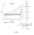
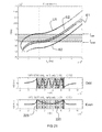
- a dispersion curve is a plot of radial frequency against the wave number associated with a supported eigenmode. The convention is to place imaginary wave numbers on the negative x-axis and real wave numbers on the positive x-axis of the graph. Radial frequency is plotted on the y-axis of the graph.
- the dispersion curves for the electrode region (dashed line) and the external region (solid line) are given. They are different from one another, because the regions have a different layer stack - at a minimum, one of the top or bottom electrodes is absent from the external region.
- Each dispersion curve crosses the y-axis at one or more so-called "cut-off" frequencies.
- the most interesting frequency regime is immediately above the fundamental Thickness-Extensional (TE1) cut-off frequency of the electrode region. For the type-I dispersion in Fig.1 , this is the upper cutoff frequency.
- the electrode region must exhibit a real-valued wave number at the relevant eigenfrequency, while the external region must present a complex-valued wave number at the same frequency.
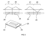
- the eigenmodes again consist of sinusoidal dependencies in the electrode areas 21 , 26 and exponential functions in the non-electrode region, decaying from the edge. In the gap between the resonators, exponentially decaying functions come from both sides.
- the eigenmodes can again be derived, but now for the system of coupled resonators.
- each eigenmode has its associated eigenfrequency.
- Fig. 3 shows two eigenmodes of such an LBAW resonator consisting of two coupled resonators. The plots indicate the particle displacement associated with each eigenmode. Note that these two eigenmodes are fundamentally different from one another. In the first (shown on the left), the particles in the first resonator and second resonator vibrate in phase. In the second (shown on the right), they vibrate in anti-phase.
- the system may exhibit either an even or an odd response. If the excitation frequency is equal to an even mode eigenfrequency, then the particle vibration in the second electrode is the same as the first electrode; in a pure odd mode response, the particle vibration has the same amplitude, but opposite sign (polarity). Not only are the amplitudes of particle vibration the same for both resonators, but also the amplitudes of voltage and current at the electrodes. In effect, at these frequencies, there is complete electrical signal transfer. From the perspective of filter-design, the eigenmodes which provide complete electrical signal transfer form the pass-band.
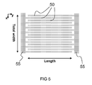
- each electrode comprises a plurality of fingers 50, of uniform width, connected to a busbar 55.
- an LBAW device should be designed to trap at least two eigenmodes.
- the laterally-coupled device contrasts with a conventional BAW device: for a conventional BAW device, trapping of one eigenmode is sufficient.
- the reason for trapping a plurality of modes is to provide increased bandwidth: if an eigenmode is trapped and is effectively excited by an electrical signal on the input electrodes then, for excitation around the corresponding eigenfrequency, the system will vibrate according to the mode-shape of the eigenmode. If the output electrode also has effective coupling to this eigenmode, then the mode will attract charge. As a result, electrical signal transfer from the input to the output electrodes is possible for the full range of desired frequencies.
- the modes that should be excited in the LBAW are the fundamental even mode and odd mode.
- the fundamental even mode is the (1,1)-mode: the wave function has one half sine in the width direction and one half sine in the length direction of the fingers. This mode is illustrated in the left-hand plot of Fig. 6 .
- the fundamental odd mode for an M-finger device is the (M,1)-mode, with M half sines in the width direction and one in the length direction. This mode is illustrated in the right-hand plot in Fig. 6 .
- the device of Fig. 6 is a nine-fingered coupled resonator; therefore, the fundamental odd mode is the (9,1)-mode.
- Overmodes are modes (m,n) with either m > M (overmodes in the width direction) or n>1 (overmodes in the length direction).
- the latter category in particular, should not be excited as they will appear as peaks in the transmission curve of an LBAW filter.
- Overmodes in the length-direction for the nine-fingered device of Fig. 6 are shown in Fig. 7 .
- Fig. 8 An example of this kind of energy trapping is shown in Fig. 8 .
- the dispersion curve of the electrode region is shown by the dashed line.
- the eigenfrequencies of the fundamental even mode 60 and fundamental odd mode 62 are also shown, by horizontal lines on the graph.
- a sub-optimal dispersion curve for the external and gap regions is shown by the solid curve.
- This characteristic curve has a cut-off frequency that traps the even mode 60 but is too low to trap the odd mode 62. This will not give a good pass-band response - typically, the pass-band at the high-frequency side will show undesirably high insertion loss.
- the dotted curve shows another dispersion curve for the external region. This curve has been optimised by careful design of the layer stack, such that the cut-off frequency has been shifted upward by approximately 50 MHz. Now both the fundamental even and odd eigenmodes are trapped.
- FIG. 9 shows another set of example dispersion curves.
- the first (m,3)-mode, or overmode 64 is also shown.
- the sub-optimal curve (solid curve) for the external region has a cut-off frequency too high to reject this overmode. Trapping of overmodes typically gives rise to unwanted peaks in the frequency response, outside the pass-band.
- the dispersion can be adjusted to lower the cut-off frequency (as shown by the dotted curve). This latter curve provides trapping for the desired fundamental (both odd and even) eigenmodes, but suppresses the overmode 64.
- the desired fundamental odd mode in an M-finger device is the (M,1) mode.
- a lower limit for the wavelength associated with this fundamental odd mode can be obtained by assuming the finger width w finger to be equal to half of the lateral wavelength ⁇ .
- the lowest overmode in the length direction is the (1,3)-mode.
- width_total is the overall width of the LBAW device and L is the length of the fingers.
- the dispersion curve has a positive slope around the cut-off frequency. Therefore, the condition for separation of the fundamental modes and overmodes is f eigen(1,3) > f eigen(M,1) ; or equivalently, k (1,3) > k (M,1) . So separation is possible if: 1 width_total 2 + 9 L 2 > 1 w finger 2 For a practical case, in which width_total ⁇ L, the first left-hand term will be dominated by the second term and the condition is thus: L ⁇ 3 ⁇ w finger This condition may or may not pose a limiting factor in practice, depending on other design considerations.
- the proper layer thickness can be derived from trial and error simulation.
- a simple one-dimensional simulation suffices. The principles of such a simulation have been described in, for example, J. Rosenbaum, "Bulk Acoustic Wave Theory and Devices” (Artech House, Boston, MA, 1988 ) and are well-known.
- the design of the layer stack for the electrode and external regions may be done as follows: a layer stack for the electrode region, consisting of at least a pair of electrodes and a piezoelectric layer, but usually also other layers (such as a reflector layer), is designed for good one-dimensional performance (proper cut-off frequency, negligible acoustic loss to the substrate, sufficient electromechanical coupling). Then, the properties - in particular the cut-off frequency - of the corresponding layer stack for the external region are investigated. Apart from the missing top electrode, this external region has the same stack as the electrode region.
- the top electrode thickness is altered (thinned) and in order to maintain the same cut-off frequency for the electrode region, the thickness of one or more other layers is adapted (increased).
- the adapted (thickened) other layer is shared by both the electrode and external regions. Therefore, the net effect is that the cut-off frequency of the external region is changed (lowered), while the cut-off frequency of the electrode region stays the same. This is a trial-and-error procedure that can be carried out with a conventional one-dimensional model.
- Electrodes are used that are thicker than would be suggested by the first method, but f cutoff.ext is decreased by adding a non-conducting layer to the external region.
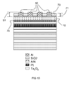
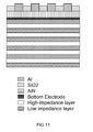
- the layer thickness 51 of the Al electrode is 455nm, while the thickness 71 of the silicon dioxide us 400 nm. As will be apparent to one skilled in the art, these value may be significantly different for other stack designs.
- Fig. 11 shows another, more general example of a layer stack design according to an embodiment.
- Type-I dispersion curves have a positive slope for wave numbers about the cut-off frequency.
- other layer stacks exhibit "Type-II" dispersion, in which the dispersion curves have negative slope in the vicinity of the cut-off frequency.
- the invention is equally applicable to devices of this type.
- Type-II dispersion the basic condition is the same: that the wave number is imaginary-valued in the external region and real-valued in the electrode-region, for the eigenfrequencies to be trapped.
- the negative slope of the curve this translates to a requirement that the cut-off frequency of the electrode region is above the desired eigenfrequencies while the cut-off frequency of the external region is below them.
- the external region may contain an extra layer, compared with the electrode region; one or more layers may be thicker in the external region than in the electrode region; or one or more layers in the external region have a higher mass density or smaller wave velocity than in the electrode region.
- the implementation of layer stacks according to the principles of the invention can be achieved using known design tools.
- the dispersion curves for a layer stack can be predicted from appropriate simulations, in one or two dimensions.
- the characteristics can be determined experimentally, for example by means of laser interferometry.
- LBAW devices according to embodiments of the first aspect of the invention have been described, it will be readily apparent to the skilled person that these examples do not imply limitations to the scope of application of the invention.
- interdigitated resonator structures have been described which have uniform finger-width, the invention is equally applicable to cases in which the widths of different fingers vary or the width of a given finger varies along its length.
- the layer stacks of the gap (the portion between the electrodes) and the external or remaining portion (surrounding the electrodes and gap) may be the same or different.
- the current inventors have also recognised that the eigenmodes trapped and their mode-shapes can be influenced through independent control of the dispersion characteristics in the external portion as compared to the gap portion. Both these regions lack at least one of the two electrode layers; however, the current inventors have recognised that the layer stacks of the two regions can be made different, such that they no longer share the same dispersion characteristics.
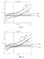
- Fig. 12 shows a set of simulated dispersion curves for a device not having the features of this aspect of the invention.
- the dispersion curves of Fig. 12 relate to a LBAW device in which the electrode region has dispersion characteristic E and the gap region and remaining (external) region has dispersion characteristic U1.
- the eigenfrequencies of the trapped eigenmodes are indicated by the solid horizontal lines.
- the lowest eigenfrequency (1901 MHz) corresponds to the fundamental even mode and the highest trapped eigenfrequency (1945MHz) corresponds to the fundamental odd eigenmode.
- Fig. 13 shows a similar set of simulated dispersion curves, for a device according to an embodiment of the second aspect of the invention. That is, the electrode regions have dispersion characteristic E; the external (remaining) portion has dispersion U1; while the gap region between the electrodes has dispersion U2.
- the frequency difference between the corresponding highest (1940MHz) and lowest (1884MHz) trapped eigenmodes has been increased by approximately 25%. This means that the bandwidth provided by the filter is correspondingly increased.
- the dispersion characteristics of the gap and the electrodes are nearly the same. Therefore, eigenmodes can be expected to exhibit a sinusoidal wave function in the gaps. At the same time, the dispersion of the remaining portion is preserved, so that this region presents an imaginary wave number. Thus, the eigenmode still exhibits an exponential wave function in this region, ensuring correct trapping.
- the dispersions of gap and external region must be made different. This means that the layer stacks for these two regions are different. Taking the layer stack of the remaining portion starting point, the task is to provide a gap region with lower cut-off frequency (assuming the device exhibits Type-I dispersion, as is the case for Figs. 12 and 13 ).
- Ways of reducing the cut-off frequency of the layer stack include: increasing the thickness of one or more layers; or adding an extra layer, usually on top of the layer stack.
- any extra layer should preferably be of insulating material.
- the restriction that the extra layer is not a metal could be a substantial limitation for a conventional BAW device.
- the layer stack design of the electrode region typically results in a relatively thick top electrode layer (for example, 100nm or more) with a high mass density (tungsten and platinum are commonly favoured materials).
- tungsten and platinum are commonly favoured materials.
- impractically thick dielectrics would be required in order to bring the cut-off frequency for the gaps to a similar value as for the electrodes.
- a light metal such as aluminium
- the thickness of this electrode layer can be dictated by criteria other than acoustics - for example, the thickness can be chosen to provide a sufficiently low electrical resistance.
- the gaps between the electrodes can be filled (partially or completely) with a dielectric with mass density and thickness such that the cut-off frequencies of the gap region and the electrode region have the desired (small) frequency difference, as in Fig. 13 .
- a light metal such as aluminium
- matching of cut-off frequencies can be achieved with reasonable thickness values of the dielectric material filling materials in the gap.
- the dielectric material there are no severe requirements for the dielectric material, apart from the fact that its intrinsic acoustic quality factor should be well above 1500: silicon dioxide, silicon nitride, and aluminium nitride all meet this requirement. It is preferable that the acoustic properties of the dielectric material are similar to those of the top electrode layer. This allows the design to use the same thickness of material in both regions, which can make the device easier to manufacture (see below).
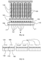
- a LBAW device An example of a LBAW device according to such an embodiment is shown in Fig. 14 .
- the first 120 and second 125 top electrodes have an interdigitated pattern.
- the top electrodes are laid on a layer of piezoelectric material 110, beneath which lies the bottom electrode 130.
- the gap between the first and second top electrodes is filled with a non-conducting material 150.
- the thickness of this is chosen to match the dispersion characteristic U2 of the gap region to the characteristic E of the electrode region.
- the external region has dispersion U1.
- CMP Chemical-Mechanical Polishing
- top electrodes 120 and 125 are fabricated on top of the piezoelectric layer 110, beneath which lies the bottom electrode 130.
- the bottom electrode is located above a reflector layer 160.
- a layer of dielectric material 150 is deposited over the top electrodes 120 and 125 and exposed (non-electrode) portions of the piezoelectric layer 110. This step is shown in the middle diagram of Fig. 15 .
- CMP is then performed, resulting in the layer structure shown in the right-hand diagram. In this case the dielectric in the gap region is intended to have the same thickness as the electrodes; therefore the top electrode material could conveniently serve as an etch-stop detector.
- Fig. 16 shows a further example of a suitable set of processing steps.
- an additional sacrificial layer 170 is provided on top of the top electrodes 120 and 125. All other layers are as shown in Fig. 15 .
- the sacrificial layer is used for etch-stop detection, therefore CMP stops when the top of this layer is exposed.
- the sacrificial layer is removed in a selective etch step, as shown in the far right-hand diagram of Fig. 16 .
- the use of a sacrificial layer allows accurate control of the thickness of the dielectric in the gap region, even when the design calls for a thickness greater than that of the top electrodes. This allows greater flexibility and design freedom in the choice of materials and thicknesses.
- the second aspect of the invention is equally applicable to the design of LBAW devices having Type-II dispersion.
- the conditions to be satisfied by the various cut-off frequencies will be reversed.
- the cut-off frequency in the gap portion is reduced, compared to the cut-off frequency in the remaining portion.
- the gap should have a higher cut-off frequency than the external region.
- each finger of both electrode portions has a first segment at the finger-tip and a second segment, comprising the remainder of the length of the electrode, which has a different layer structure to the first segment.
- the first segment 222 at each finger tips has a dispersion characteristic with a lower cut-off frequency than the remainder of the finger (second segments 220).
- the gap region 255 has the same layer structure (and therefore dispersion characteristic) as the external region surrounding the coupled resonators.
- the variation in the dispersion characteristic at the finger tips has the effect of changing the shape of the eigenmodes supported by the device.
- the mode shape along the length direction of the fingers is changed, so that it is more uniform.
- Fig. 6 it can be seen that the fundamental odd and even modes obtained with a simple interdigitated layout have a sinusoidal profile (with a half-sine period) in the length direction.
- this sinusoidal mode-shape can be flattened and spread to present a more uniform profile over the length of each finger.
- the shapes of the overmodes (m,n), where n is greater than 1, are modified so that they are sinusoids with a full wavelength over the length of the fingers. This is in contrast with Fig. 7 , which shows overmodes with an odd number of half-sines. The excitation strength of the modified (full-wavelength) overmodes is very low.
- Fig. 18 illustrates a variation on the layout of Fig. 17 .
- both the finger tips 222 and the adjacent segments 256 of the gap 255 have adapted dispersion characteristics (that is, adapted cut-off frequencies).
- the cut-off frequency of the first segments (finger tips 222) of the electrode portions is lower than that of the second segment (remainder 220).
- the cut-off frequency of the first segments of the gap (gap-ends 256) is lower than that of the remainder of the gap 255.
- the cut-off frequencies of the electrode finger tips 222 and the gap-ends 256 may be the same.
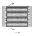
- Fig. 19 shows another variation. Compared with the example of Fig. 18 , the dispersion characteristic of the gap region 250 is now modified with respect to the external region - that is, the remaining portion, surrounding the LBAW device. Therefore, this example combines this third aspect of the invention with the second aspect described previously above.
- Fig. 21 assumes that the outer segments 223 of the electrode portions have a dispersion characteristic E2.
- the remaining, inner fingers 220 have dispersion E1.
- the gaps have dispersion U2, while the remaining portion (external region) has dispersion U1.
- the cut-off frequency of U1 is the highest, followed by U2, E1 and E2, in that order.
- the mode-shapes of the two fundamental modes are illustrated below the dispersion graph.
- the dispersion characteristic E1 for the inner fingers presents a real-valued wave number at the eigenfrequencies of interest.
- the characteristic U1 exhibits an imaginary wave number. This is as described previously for the first aspect of the invention.
- the corresponding wave numbers in the gap region are real (see U2) - to the extent that U2 matches E1. This is as described previously for the second aspect of the invention.
- the wave numbers of the modified outermost fingers are also real (see E2), but with values greater than either the inner electrodes or the gap region U2. This corresponds to a sinusoidal wave function with a shorter wavelength.
- Modification of the outer edges of the electrode portions may be of particular benefit if the total width of the LBAW device is small. In an interdigitated layout, this may be because the number of fingers is low, or because the fingers and gaps are relatively narrow.
- the definition of "small” depends on the actual dispersion characteristics. In the context of the exemplary dispersion curves presented here, a total width of less than 30 microns can be considered small. However, where dispersion curves are steeper, wider devices than this may still be considered small.
- modification of the dispersion characteristic can be achieved by modifying the layer structure in the relevant portion of the LBAW device.
- the examples of Figs. 17-20 use a frame region, where either the finger tips; part of the outermost fingers; or both are adapted.
- the frame region should have a reduced cut-off frequency. This can be achieved, for example, by depositing an extra layer on top of the peripheral portions. Such a layer may be conducting or non-conducting. If it is conducting it may comprise part of the electrode.
- the cut-off frequency of the peripheral regions should instead be greater than that of the rest of the electrode fingers.
Landscapes
- Physics & Mathematics (AREA)
- Acoustics & Sound (AREA)
- Chemical & Material Sciences (AREA)
- Crystallography & Structural Chemistry (AREA)
- Engineering & Computer Science (AREA)
- Manufacturing & Machinery (AREA)
- Piezo-Electric Or Mechanical Vibrators, Or Delay Or Filter Circuits (AREA)
Priority Applications (3)
| Application Number | Priority Date | Filing Date | Title |
|---|---|---|---|
| EP09170753A EP2299593A1 (fr) | 2009-09-18 | 2009-09-18 | Dispositif d'ondes acoustiques de volume couplées latéralement |
| EP09179278A EP2299592A1 (fr) | 2009-09-18 | 2009-12-15 | Procédé de fabrication de dispositif d'ondes acoustiques de volume |
| US12/968,020 US8409996B2 (en) | 2009-09-18 | 2010-12-14 | Method of manufacturing a bulk acoustic wave device |
Applications Claiming Priority (1)
| Application Number | Priority Date | Filing Date | Title |
|---|---|---|---|
| EP09170753A EP2299593A1 (fr) | 2009-09-18 | 2009-09-18 | Dispositif d'ondes acoustiques de volume couplées latéralement |
Publications (1)
| Publication Number | Publication Date |
|---|---|
| EP2299593A1 true EP2299593A1 (fr) | 2011-03-23 |
Family
ID=41821933
Family Applications (2)
| Application Number | Title | Priority Date | Filing Date |
|---|---|---|---|
| EP09170753A Withdrawn EP2299593A1 (fr) | 2009-09-18 | 2009-09-18 | Dispositif d'ondes acoustiques de volume couplées latéralement |
| EP09179278A Withdrawn EP2299592A1 (fr) | 2009-09-18 | 2009-12-15 | Procédé de fabrication de dispositif d'ondes acoustiques de volume |
Family Applications After (1)
| Application Number | Title | Priority Date | Filing Date |
|---|---|---|---|
| EP09179278A Withdrawn EP2299592A1 (fr) | 2009-09-18 | 2009-12-15 | Procédé de fabrication de dispositif d'ondes acoustiques de volume |
Country Status (2)
| Country | Link |
|---|---|
| US (1) | US8409996B2 (fr) |
| EP (2) | EP2299593A1 (fr) |
Cited By (21)
| Publication number | Priority date | Publication date | Assignee | Title |
|---|---|---|---|---|
| US8188810B2 (en) | 2004-12-22 | 2012-05-29 | Avago Technologies Wireless Ip (Singapore) Pte. Ltd. | Acoustic resonator performance enhancement using selective metal etch |
| US8248185B2 (en) | 2009-06-24 | 2012-08-21 | Avago Technologies Wireless Ip (Singapore) Pte. Ltd. | Acoustic resonator structure comprising a bridge |
| US8330325B1 (en) | 2011-06-16 | 2012-12-11 | Avago Technologies Wireless Ip (Singapore) Pte. Ltd. | Bulk acoustic resonator comprising non-piezoelectric layer |
| US8350445B1 (en) | 2011-06-16 | 2013-01-08 | Avago Technologies Wireless Ip (Singapore) Pte. Ltd. | Bulk acoustic resonator comprising non-piezoelectric layer and bridge |
| US8575820B2 (en) | 2011-03-29 | 2013-11-05 | Avago Technologies General Ip (Singapore) Pte. Ltd. | Stacked bulk acoustic resonator |
| US8796904B2 (en) | 2011-10-31 | 2014-08-05 | Avago Technologies General Ip (Singapore) Pte. Ltd. | Bulk acoustic resonator comprising piezoelectric layer and inverse piezoelectric layer |
| US8902023B2 (en) | 2009-06-24 | 2014-12-02 | Avago Technologies General Ip (Singapore) Pte. Ltd. | Acoustic resonator structure having an electrode with a cantilevered portion |
| US8922302B2 (en) | 2011-08-24 | 2014-12-30 | Avago Technologies General Ip (Singapore) Pte. Ltd. | Acoustic resonator formed on a pedestal |
| US8962443B2 (en) | 2011-01-31 | 2015-02-24 | Avago Technologies General Ip (Singapore) Pte. Ltd. | Semiconductor device having an airbridge and method of fabricating the same |
| US8981876B2 (en) | 2004-11-15 | 2015-03-17 | Avago Technologies General Ip (Singapore) Pte. Ltd. | Piezoelectric resonator structures and electrical filters having frame elements |
| US9048812B2 (en) | 2011-02-28 | 2015-06-02 | Avago Technologies General Ip (Singapore) Pte. Ltd. | Bulk acoustic wave resonator comprising bridge formed within piezoelectric layer |
| US9083302B2 (en) | 2011-02-28 | 2015-07-14 | Avago Technologies General Ip (Singapore) Pte. Ltd. | Stacked bulk acoustic resonator comprising a bridge and an acoustic reflector along a perimeter of the resonator |
| US9136818B2 (en) | 2011-02-28 | 2015-09-15 | Avago Technologies General Ip (Singapore) Pte. Ltd. | Stacked acoustic resonator comprising a bridge |
| US9148117B2 (en) | 2011-02-28 | 2015-09-29 | Avago Technologies General Ip (Singapore) Pte. Ltd. | Coupled resonator filter comprising a bridge and frame elements |
| US9154112B2 (en) | 2011-02-28 | 2015-10-06 | Avago Technologies General Ip (Singapore) Pte. Ltd. | Coupled resonator filter comprising a bridge |
| US9203374B2 (en) | 2011-02-28 | 2015-12-01 | Avago Technologies General Ip (Singapore) Pte. Ltd. | Film bulk acoustic resonator comprising a bridge |
| US9243316B2 (en) | 2010-01-22 | 2016-01-26 | Avago Technologies General Ip (Singapore) Pte. Ltd. | Method of fabricating piezoelectric material with selected c-axis orientation |
| US9425764B2 (en) | 2012-10-25 | 2016-08-23 | Avago Technologies General Ip (Singapore) Pte. Ltd. | Accoustic resonator having composite electrodes with integrated lateral features |
| US9444426B2 (en) | 2012-10-25 | 2016-09-13 | Avago Technologies General Ip (Singapore) Pte. Ltd. | Accoustic resonator having integrated lateral feature and temperature compensation feature |
| US9525397B2 (en) | 2011-03-29 | 2016-12-20 | Avago Technologies General Ip (Singapore) Pte. Ltd. | Acoustic resonator comprising acoustic reflector, frame and collar |
| US10476469B2 (en) | 2016-02-17 | 2019-11-12 | Board of Trustees of the Univsity of Illinois | Spurious-mode-free, laterally-vibrating microelectromechanical system resonators |
Families Citing this family (12)
| Publication number | Priority date | Publication date | Assignee | Title |
|---|---|---|---|---|
| US9673778B2 (en) | 2009-06-24 | 2017-06-06 | Avago Technologies General Ip (Singapore) Pte. Ltd. | Solid mount bulk acoustic wave resonator structure comprising a bridge |
| US9520856B2 (en) | 2009-06-24 | 2016-12-13 | Avago Technologies General Ip (Singapore) Pte. Ltd. | Acoustic resonator structure having an electrode with a cantilevered portion |
| US9450561B2 (en) | 2009-11-25 | 2016-09-20 | Avago Technologies General Ip (Singapore) Pte. Ltd. | Bulk acoustic wave (BAW) resonator structure having an electrode with a cantilevered portion and a piezoelectric layer with varying amounts of dopant |
| FI123640B (fi) * | 2010-04-23 | 2013-08-30 | Teknologian Tutkimuskeskus Vtt | Laajakaistainen akustisesti kytketty ohutkalvo-BAW-suodin |
| US9099983B2 (en) | 2011-02-28 | 2015-08-04 | Avago Technologies General Ip (Singapore) Pte. Ltd. | Bulk acoustic wave resonator device comprising a bridge in an acoustic reflector |
| JP5686196B2 (ja) * | 2011-08-29 | 2015-03-18 | トヨタ自動車株式会社 | 微粒子センサ及び微粒子センサの製造方法 |
| US9608592B2 (en) | 2014-01-21 | 2017-03-28 | Avago Technologies General Ip (Singapore) Pte. Ltd. | Film bulk acoustic wave resonator (FBAR) having stress-relief |
| US10557784B2 (en) * | 2015-11-20 | 2020-02-11 | Ford Global Technologies, Llc | Method and system for exhaust particulate matter sensing |
| RU2017120043A (ru) * | 2016-06-20 | 2018-12-07 | Форд Глобал Текнолоджиз, Ллк | Способ и система для обнаружения твердых частиц в отработавших газах |
| US10797676B2 (en) | 2017-09-15 | 2020-10-06 | Qualcomm Incorporated | Acoustic resonator with enhanced boundary conditions |
| US11146241B2 (en) * | 2019-02-08 | 2021-10-12 | Vtt Technical Research Centre Of Finland Ltd | Low loss acoustic device |
| US11223341B2 (en) * | 2019-10-22 | 2022-01-11 | Vtt Technical Research Centre Of Finland Ltd | Suppressing parasitic sidebands in lateral bulk acoustic wave resonators |
Family Cites Families (16)
| Publication number | Priority date | Publication date | Assignee | Title |
|---|---|---|---|---|
| JPS6471208A (en) * | 1987-09-11 | 1989-03-16 | Toshiba Corp | Piezoelectric thin film resonator |
| US5692279A (en) * | 1995-08-17 | 1997-12-02 | Motorola | Method of making a monolithic thin film resonator lattice filter |
| DE69836011T2 (de) * | 1998-01-16 | 2007-05-24 | Mitsubishi Denki K.K. | Piezoelektrische dünnschichtanordnung |
| US6601276B2 (en) | 2001-05-11 | 2003-08-05 | Agere Systems Inc. | Method for self alignment of patterned layers in thin film acoustic devices |
| DE10124349A1 (de) | 2001-05-18 | 2002-12-05 | Infineon Technologies Ag | Piezoelektrische Resonatorvorrichtung mit Verstimmungsschichtfolge |
| US7213359B2 (en) | 2002-03-26 | 2007-05-08 | Fabbrica D'armi Pietro Beretta S.P.A | Additional safety device for sear mechanism for firearms |
| US6881351B2 (en) * | 2003-04-22 | 2005-04-19 | Freescale Semiconductor, Inc. | Methods for contacting conducting layers overlying magnetoelectronic elements of MRAM devices |
| DE10331351A1 (de) | 2003-07-11 | 2005-01-27 | Mtu Aero Engines Gmbh | Verfahren und Vorrichtung zum Herstellen einer korrosionsbeständigen und oxidationsbeständigen Beschichtung sowie Bauteil mit einer solchen Beschichtung |
| JP4321754B2 (ja) | 2003-07-31 | 2009-08-26 | Tdk株式会社 | 圧電共振器およびそれを用いたフィルタ |
| WO2005034345A1 (fr) | 2003-10-06 | 2005-04-14 | Philips Intellectual Property & Standards Gmbh | Structure de resonateur et son procede de fabrication |
| US8938141B2 (en) * | 2004-07-30 | 2015-01-20 | University Of Connecticut | Tunable resonant leaky-mode N/MEMS elements and uses in optical devices |
| US7248131B2 (en) * | 2005-03-14 | 2007-07-24 | Avago Technologies Wireless Ip (Singapore) Pte. Ltd. | Monolithic vertical integration of an acoustic resonator and electronic circuitry |
| WO2006126168A1 (fr) | 2005-05-27 | 2006-11-30 | Nxp B.V. | Dispositif resonateur d'onde acoustique en volume |
| CN101278479B (zh) | 2005-09-30 | 2011-04-13 | Nxp股份有限公司 | 薄膜体声波(baw)谐振器或相关改进 |
| US8487719B2 (en) | 2008-04-29 | 2013-07-16 | Triquint Semiconductor, Inc. | Bulk acoustic wave resonator |
| EP2237416A1 (fr) | 2009-03-30 | 2010-10-06 | Nxp B.V. | Dispositif comportant un symétriseur électroacoustique |
-
2009
- 2009-09-18 EP EP09170753A patent/EP2299593A1/fr not_active Withdrawn
- 2009-12-15 EP EP09179278A patent/EP2299592A1/fr not_active Withdrawn
-
2010
- 2010-12-14 US US12/968,020 patent/US8409996B2/en active Active
Non-Patent Citations (2)
| Title |
|---|
| J. ROSENBAUM: "Bulk Acoustic Wave Theory and Devices", 1988, ARTECH HOUSE |
| No Search * |
Cited By (23)
| Publication number | Priority date | Publication date | Assignee | Title |
|---|---|---|---|---|
| US8981876B2 (en) | 2004-11-15 | 2015-03-17 | Avago Technologies General Ip (Singapore) Pte. Ltd. | Piezoelectric resonator structures and electrical filters having frame elements |
| US8188810B2 (en) | 2004-12-22 | 2012-05-29 | Avago Technologies Wireless Ip (Singapore) Pte. Ltd. | Acoustic resonator performance enhancement using selective metal etch |
| US8248185B2 (en) | 2009-06-24 | 2012-08-21 | Avago Technologies Wireless Ip (Singapore) Pte. Ltd. | Acoustic resonator structure comprising a bridge |
| US8902023B2 (en) | 2009-06-24 | 2014-12-02 | Avago Technologies General Ip (Singapore) Pte. Ltd. | Acoustic resonator structure having an electrode with a cantilevered portion |
| US9243316B2 (en) | 2010-01-22 | 2016-01-26 | Avago Technologies General Ip (Singapore) Pte. Ltd. | Method of fabricating piezoelectric material with selected c-axis orientation |
| US8962443B2 (en) | 2011-01-31 | 2015-02-24 | Avago Technologies General Ip (Singapore) Pte. Ltd. | Semiconductor device having an airbridge and method of fabricating the same |
| US9859205B2 (en) | 2011-01-31 | 2018-01-02 | Avago Technologies General Ip (Singapore) Pte. Ltd. | Semiconductor device having an airbridge and method of fabricating the same |
| US9203374B2 (en) | 2011-02-28 | 2015-12-01 | Avago Technologies General Ip (Singapore) Pte. Ltd. | Film bulk acoustic resonator comprising a bridge |
| US9154112B2 (en) | 2011-02-28 | 2015-10-06 | Avago Technologies General Ip (Singapore) Pte. Ltd. | Coupled resonator filter comprising a bridge |
| US9148117B2 (en) | 2011-02-28 | 2015-09-29 | Avago Technologies General Ip (Singapore) Pte. Ltd. | Coupled resonator filter comprising a bridge and frame elements |
| US9048812B2 (en) | 2011-02-28 | 2015-06-02 | Avago Technologies General Ip (Singapore) Pte. Ltd. | Bulk acoustic wave resonator comprising bridge formed within piezoelectric layer |
| US9083302B2 (en) | 2011-02-28 | 2015-07-14 | Avago Technologies General Ip (Singapore) Pte. Ltd. | Stacked bulk acoustic resonator comprising a bridge and an acoustic reflector along a perimeter of the resonator |
| US9136818B2 (en) | 2011-02-28 | 2015-09-15 | Avago Technologies General Ip (Singapore) Pte. Ltd. | Stacked acoustic resonator comprising a bridge |
| US8575820B2 (en) | 2011-03-29 | 2013-11-05 | Avago Technologies General Ip (Singapore) Pte. Ltd. | Stacked bulk acoustic resonator |
| US9525397B2 (en) | 2011-03-29 | 2016-12-20 | Avago Technologies General Ip (Singapore) Pte. Ltd. | Acoustic resonator comprising acoustic reflector, frame and collar |
| US8350445B1 (en) | 2011-06-16 | 2013-01-08 | Avago Technologies Wireless Ip (Singapore) Pte. Ltd. | Bulk acoustic resonator comprising non-piezoelectric layer and bridge |
| US8330325B1 (en) | 2011-06-16 | 2012-12-11 | Avago Technologies Wireless Ip (Singapore) Pte. Ltd. | Bulk acoustic resonator comprising non-piezoelectric layer |
| US8922302B2 (en) | 2011-08-24 | 2014-12-30 | Avago Technologies General Ip (Singapore) Pte. Ltd. | Acoustic resonator formed on a pedestal |
| US8796904B2 (en) | 2011-10-31 | 2014-08-05 | Avago Technologies General Ip (Singapore) Pte. Ltd. | Bulk acoustic resonator comprising piezoelectric layer and inverse piezoelectric layer |
| US9425764B2 (en) | 2012-10-25 | 2016-08-23 | Avago Technologies General Ip (Singapore) Pte. Ltd. | Accoustic resonator having composite electrodes with integrated lateral features |
| US9444426B2 (en) | 2012-10-25 | 2016-09-13 | Avago Technologies General Ip (Singapore) Pte. Ltd. | Accoustic resonator having integrated lateral feature and temperature compensation feature |
| US10476469B2 (en) | 2016-02-17 | 2019-11-12 | Board of Trustees of the Univsity of Illinois | Spurious-mode-free, laterally-vibrating microelectromechanical system resonators |
| US11496110B2 (en) | 2016-02-17 | 2022-11-08 | The Board Of Trustees Of The University Of Illinois | Spurious-mode-free, laterally-vibrating microelectromechanical system resonators |
Also Published As
| Publication number | Publication date |
|---|---|
| US8409996B2 (en) | 2013-04-02 |
| EP2299592A1 (fr) | 2011-03-23 |
| US20110315654A1 (en) | 2011-12-29 |
Similar Documents
| Publication | Publication Date | Title |
|---|---|---|
| EP2299593A1 (fr) | Dispositif d'ondes acoustiques de volume couplées latéralement | |
| US6812619B1 (en) | Resonator structure and a filter comprising such a resonator structure | |
| US8230562B2 (en) | Method of fabricating an acoustic resonator comprising a filled recessed region | |
| EP2628246B1 (fr) | Filtre à ondes acoustiques de volume à couches minces, à couplage acoustique à large bande | |
| US9385684B2 (en) | Acoustic resonator having guard ring | |
| EP2777153B1 (fr) | Filtre d'onde acoustique de volume couplé latéralement ayant des caractéristiques de bande passante améliorées | |
| EP1258989B1 (fr) | Procédé d'accordage des résonateurs à ondes acoustiques de volume | |
| EP1575165B1 (fr) | Filtre à ondes acoustiques de volume et méthode pour éliminer le passage de signaux indésirables dans la bande latérale | |
| EP2561613B1 (fr) | Filtre à ondes acoustiques de volume (baw) à film mince couplé acoustiquement à large bande | |
| CN112673568B (zh) | 用于调整声波谐振器的频率响应的负荷谐振器 | |
| US20110121916A1 (en) | Hybrid bulk acoustic wave resonator | |
| CN112673569B (zh) | 双级横向体声波滤波器 | |
| US20100277257A1 (en) | Acoustic resonator performance enhancement using selective metal etch | |
| GB2427773A (en) | Acoustic resonator performance enhancement using alternating frame structure | |
| US20210234528A1 (en) | Fifth-generation (5g)-focused piezoelectric resonators and filters | |
| CN112689956B (zh) | 横向体声波滤波器 | |
| CN112425073A (zh) | 具有虚假模式抑制的高q baw谐振器 | |
| US11894827B2 (en) | Loaded series resonators for adjusting frequency response of acoustic wave resonators | |
| WO2021078917A1 (fr) | Filtre à ondes acoustiques de volume latérales à deux étages avec couplage capacitif de contre-électrode | |
| US20160268999A1 (en) | Tunable q resonator |
Legal Events
| Date | Code | Title | Description |
|---|---|---|---|
| PUAI | Public reference made under article 153(3) epc to a published international application that has entered the european phase |
Free format text: ORIGINAL CODE: 0009012 |
|
| AK | Designated contracting states |
Kind code of ref document: A1 Designated state(s): AT BE BG CH CY CZ DE DK EE ES FI FR GB GR HR HU IE IS IT LI LT LU LV MC MK MT NL NO PL PT RO SE SI SK SM TR |
|
| AX | Request for extension of the european patent |
Extension state: AL BA RS |
|
| 17P | Request for examination filed |
Effective date: 20110923 |
|
| 17Q | First examination report despatched |
Effective date: 20111013 |
|
| STAA | Information on the status of an ep patent application or granted ep patent |
Free format text: STATUS: THE APPLICATION IS DEEMED TO BE WITHDRAWN |
|
| 18D | Application deemed to be withdrawn |
Effective date: 20120224 |