-
This invention relates to bulk acoustic wave devices. In particular, it relates to lateral coupling of energy in such devices.
-
For mobile communication applications with high demands on RadioFrequency (RF) filter selectivity, thin-film Bulk Acoustic Wave (BAW) filters are the technology of choice. Examples of this trend include narrow band CDMA and WCDMA mobile devices equipped with BAW filters. Such filters are particularly suitable for communication standards with carrier frequencies above 1 GHz and having stringent specifications on frequency selectivity.
-
An additional desirable feature for a BAW device is transformation of an unbalanced input signal into two balanced output signals. This action is called "balun" (balanced-to-unbalanced or vice versa) functionality. If a circuit utilises conventional BAW devices for filtering, then a separate balun component is required. Balun functionality was, in the past, traditionally achieved by magnetic coupling - using a transformer. As is well known, the DC levels at either side of a transformer can be chosen independently. It is desirable to provide similar decoupling using acoustic coupling between BAW devices, rather than magnetic coupling between transformer coils.
-
One proposal to achieve integrated balun functionality is the acoustically-coupled BAW. Two variations of this idea have been proposed: vertically and laterally coupled BAWs. The vertical version (hereinafter VBAW) is difficult and expensive to produce. On the other hand, laterally coupled BAW s (hereinafter LBAWs) are potentially cheap, but good performance devices have not been reported: neither good frequency selectivity, nor balun functionality have been shown for LBAWs.
-
Even without the added feature of balun functionality, acoustically coupled BAW filters have benefits for design flexibility: by adding shunt capacitances, the designer has full control of the notches outside the pass-band, whereas in conventional BAW filters they are fixed by the device technology.
-
It is therefore desired to produce a coupled BAW device having good frequency selectivity properties, which is also easy and inexpensive to manufacture.
-
According to an aspect of the current invention, there is provided a laterally-coupled bulk acoustic wave device for acoustic coupling of signals, the device having eigenmodes with associated eigenfrequencies in a desired pass-band, the device comprising: a piezoelectric layer; a first electrode disposed on the piezoelectric layer defining a first electrode portion of the device; and a second electrode disposed on the piezoelectric layer defining a second electrode portion of the device, whereby a gap portion of the device is defined between the first and second electrodes and a remaining portion of the device is defined around the electrodes, wherein a layer structure of the device is adapted such that in the remaining portion the wave number for each of a plurality of desired eigenmodes within the pass-band is an imaginary number, so as to enhance the quality factor of these eigenmodes.
-
The device is adapted, by careful design of the layer stack, to trap at least two desired eigenmodes. The layer stack is chosen to give specific dispersion properties - namely, that the wave number in the external region, around the electrodes, has an imaginary value for the eigenfrequencies of interest. This dispersion property is one condition for successful energy trapping of modes. By trapping at least two modes in this way, the resulting device provides improved pass-band characteristics when used as a filter. Dips in the pass-band are reduced by the trapping of multiple eigenmodes in the band.
-
The device may be further adapted such that in the remaining portion the wave number for at least one undesired eigenmode outside the pass-band is a real number, so as to reduce the quality factor of these eigenmodes, so as to reduce the impact of these eigenmodes on the LBAW filter characteristics.
-
Since an imaginary wave number in the external region is a requirement for trapping of eigenmodes, when the wave number is instead real, the mode is suppressed. By adapting the device layer structure to meet this further dispersion requirement, the filter characteristics can be improved still further. In particular, spurious peaks outside the pass band, caused by unwanted modes, can be avoided.
-
Preferably, the plurality of desired eigenmodes comprises the fundamental even eigenmode and the fundamental odd eigenmode of the device.
-
These two modes represent the most useful frequency regime for a laterally coupled bulk acoustic wave resonator device.
-
Preferably, at least one undesired eigenmode comprises an over-mode of higher order than the fundamental eigenmodes.
-
It is typically not useful to include such harmonic eigenfrequencies in the pass-band and they are therefore suppressed.
-
The layer structure may be adapted by selecting the material and/or the thickness of at least one of the first and second electrodes, so as to achieve the desired dispersion characteristic in the remaining portion.
-
This mechanism for controlling the dispersion is particularly beneficial when the remaining portion and the electrode portion differ only by the presence of an electrode layer in the electrode portion. In this case, one possible design methodology is to choose the thickness of the electrode to achieve a desired offset of the cut-off frequency in the remaining portion from that of the electrode portion. The thickness of one or more layers in the common layer structure can then be designed so that the dispersion characteristic of electrode region matches the desired pass-band parameters.
-
This provides one convenient way of adapting the dispersion characteristics to match those desired. In this way, the device can be provided with improved filtering properties without any increase in complexity of the manufacturing process, since no additional layers need be provided.
-
The layer structure may be adapted by at least one of: providing a layer of different thickness in the remaining portion as compared with the first and second electrode portions; providing an additional layer in the remaining portion as compared with the first and second electrode portions; or providing a layer in the remaining portion having a greater mass-density and/or lesser wave velocity than a corresponding layer in the first and second electrode portions, so as to achieve the desired dispersion characteristic in the remaining portion.
-
Modification of the layer structure provides more flexibility in the choice of dispersion characteristics and therefore potentially more complete control of the device filter properties.
-
The first and second electrodes may be arranged in a pattern comprising a plurality of interdigitated fingers.
-
This is one advantageous layout for an LBAW device, since it allows the coupling between input and output electrodes (via acoustic coupling) to be maximised.
-
The width of at least one finger of the plurality of fingers may be different from at least one other.
-
This can provide for further degrees of freedom in the design, allowing better control over the eigenmodes supported and their mode-shapes, as well as their eigenfrequencies.
-
According to a second aspect of the invention, there is provided a laterally-coupled bulk acoustic wave device for acoustic coupling of signals at frequencies in a desired pass-band, the device comprising: a piezoelectric layer; a first electrode disposed on the piezoelectric layer defining a first electrode portion of the device; and a second electrode disposed on the piezoelectric layer defining a second electrode portion of the device, whereby a gap portion of the device is defined between the first and second electrodes and a remaining portion of the device is defined around the electrodes, wherein the gap portion and the remaining portion comprise different layer structures.
-
This offers a further degree of freedom to the designer. By designing the gap portion, between the electrodes, and the remaining portion, surrounding the electrodes, to have different dispersion characteristics, it may be possible to achieve greater separation between the fundamental eigenmodes trapped. This, in turn, can lead to enhanced bandwidth of the pass-band. The advantages may be particularly significant in the case that the electrodes are arranged in an interdigitated pattern.
-
The layer structure of the gap portion may be adapted such that in that portion the wave number for each of the plurality of desired eigenmodes is a real number.
-
This means that the wave function corresponding to each of the desired eigenmodes has a propagating characteristic in the gap region as well as in the electrode region. In this way, one can increase the frequency spacing between the eigenfrequencies of these eignmodes and thus increase the bandwidth of the device.
-
The cut-off frequency of the gap portion may be in the range 98% to 102% of the cut-off frequency of one of the first and second electrode portions.
-
By matching the dispersion characteristics of the gap and electrode portions, the potential mismatch between the vertical mode-shapes in the respective portions may be minimised.
-
This matching of dispersion characteristics may be advantageously achieved by providing a top layer in the gap portion, between the electrodes, comprised of material having acoustic properties similar to those of the material comprising the electrodes.
-
A top layer of material in the gap region between the electrodes can be used to make the dispersion of the gap portion similar to the dispersion of the electrode portions. If the material in the gaps between the electrodes matches the acoustic properties of the electrodes themselves, then the difference in overall thickness between gap and electrode portions may be reduced. This may lead to simplified processing during fabrication.
-
The cut-off frequency of the remaining portion may be in the range 90% to 110% of the higher cut-off frequency among the first and second electrode portions.
-
These relative differences effectively define the pass-band bandwidth. Ratios in the stated range are advantageous for typical applications, for example in telecommunications.
-
The relative difference between the cut-off frequency of the remaining portion and the eigenfrequency of the nearest among the plurality of desired eigenmodes may be in the range 1% to 3% of the eigenfrequency.
-
In this way, the cut-off frequency is placed close to the desired eigenfrequency defining the edge of the pass-band. This provides maximal suppression of out of band frequencies and a sharp transition (that is, a steep roll-off of gain in the transition band).
-
According to a third aspect of the invention, there is provided a laterally-coupled bulk acoustic wave device for acoustic coupling of signals at frequencies in a desired pass-band, the device comprising: a piezoelectric layer; a first electrode disposed on the piezoelectric layer defining a first electrode portion of the device; and a second electrode disposed on the piezoelectric layer defining a second electrode portion of the device, whereby a gap portion of the device is defined between the first and second electrodes and a remaining portion of the device is defined around the electrodes, wherein at least one of the first and the second electrode portions comprises first and second segments having different layer structures.
-
This design provides an electrode portion with a varying layer stack and hence varying dispersion characteristics. This can be used to adjust and optimise the mode-shapes of the trapped eigenmodes. A number of benefits may flow from such optimisation. Firstly, more precise control of the eigenmodes supported may be possible. For example, the electrode portions may be adapted to ensure that only the fundamental mode in the length direction of the electrode can be excited and higher order modes are suppressed. Secondly, in an embodiment where the electrodes have an interdigitated pattern, it may be possible to design the device to achieve a greater frequency separation between the first fundamental odd and even modes. This in turn can provide enhanced bandwidth of the filter pass-band. Thirdly, the relative degree of coupling of the different eigenmodes may be better controlled. This effect could be used, for example, to ensure that the input-output coupling of the fundamental odd and even modes is matched.
-
The first segment may comprise an end segment of the electrode portion, in which case: if the device has a Type-I dispersion characteristic, the cut-off frequency of the first segment is preferably less than that of the second segment; or if the device has a Type-II dispersion characteristic, the cut-off frequency of the first segment is preferably greater than that of the second segment.
-
This requirement may also be stated as follows: the layer structure of the end segment of the electrode is preferably adapted so that the dispersion characteristic in this segment presents a higher real wave number at the eigenfrequencies of interest, as compared with the wave number in the remaining (second) segment of the electrode length. This condition on the dispersion characteristics translates to different requirements on the respective cut-off frequencies, depending on whether the device is characterised by Type-I dispersion (in which the slope of the dispersion curve is positive in the vicinity of cut-off) or Type-II dispersion (in which the slope of the dispersion curve is negative in the vicinity of cut-off). This represents one potentially beneficial implementation of non-uniform electrode-portion dispersion.
-
Note that, by "end segment" of an electrode, it is meant that the first segment comprises an extremity of the electrode portion in the length direction. Here, the length direction of the electrodes is defined with reference to the gap between the first and second electrodes: the length is the direction parallel to the gap. Usually, this direction also corresponds to the length direction as it would be defined by reference to the aspect ratio of the electrode.
-
The first and second electrodes may be arranged in a pattern comprising a plurality of interdigitated fingers; and the first segment may comprise an at least partial longitudinal segment of an outermost of the plurality of interdigitated fingers, in which case: if the device has a Type-I dispersion characteristic, the cut-off frequency of the first segment may be less than that of the second segment; or if the device has a Type-II dispersion characteristic, the cut-off frequency of the first segment may be greater than that of the second segment.
-
This arrangement provides a first segment of the electrode portion lying along a peripheral finger of the interdigitated pattern and having different dispersion characteristics to a second segment of the electrode portion in the interior of the pattern. Preferably, such a first segment is provided at both extremities of the interdigitated pattern - that is, corresponding to the first and last fingers. This segment may comprise the entire outer finger or a longitudinal slice of it. The dispersion characteristics are typically chosen so that the desired eigenmodes have a real wave number in the first segment and this is higher than that found for the same eigenfrequency in the second segment. As noted above, such a condition on the dispersion characteristics translates to different requirements on the respective cut-off frequencies, depending on whether the device is characterised by Type-I or Type-II dispersion.
-
According to another aspect of the invention, there is provided a method of manufacturing a laterally-coupled bulk acoustic wave device for acoustic coupling of signals having frequencies in a desired pass-band, the device comprising: a piezoelectric layer; a first electrode disposed on the layer defining a first electrode portion of the device; and a second electrode disposed on the layer defining a second electrode portion of the device, whereby a gap portion of the device is defined between the first and second electrodes and a remaining portion of the device is defined around the electrodes, the method comprising: selecting a plurality of desired eigenmodes within the pass-band; selecting a layer structure of the device such that in the remaining portion the wave number for each of the plurality of desired eigenmodes is an imaginary number, so as to increase the quality factor of these eigenmodes; and materially producing the device having the selected layer structure.
-
The invention will now be described by way of example, with reference to the accompanying drawings, in which:
- Figure 1 shows a conventional BAW resonator and the first three associated eigenmode shapes;
- Figure 2 shows the dispersion characteristics of the device illustrated in Fig. 1 and illustrates the correspondence of the mode-shapes (in two dimensions) with the dispersion plot;
- Figure 3 shows a simple example of a laterally-coupled BAW device comprising two resonators, and an illustration of its fundamental mode-shapes in two dimensions;
- Figure 4 shows an example dispersion characteristic for a two-resonator system, together with corresponding mode-shapes;
- Figure 5 is a plan view of a two-resonator LBAW device with an interdigitated finger layout;
- Figure 6 shows the fundamental even and odd eigenmodes for an interdigitated device of the type shown in Fig. 5;
- Figure 7 shows higher eigenmodes, for the same device, which have a higher wave number in the length direction of the fingers;
- Figure 8 illustrates the design of dispersion characteristics according to an embodiment of a first aspect of the invention, so as to trap two desired eigenmodes;
- Figure 9 illustrates the design of dispersion characteristics according to an embodiment of the first aspect, so as to suppress an undesired overmode;
- Figure 10 shows an example layer structure for a device according to an embodiment;
- Figure 11 shows a second, alternative layer structure;
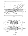
- Figure 12 shows simulated dispersion curves for an embodiment of the first aspect;
- Figure 13 shows simulated dispersion curves for an embodiment of a second aspect of the invention;
- Figure 14 illustrates an exemplary layout and layer structure for an embodiment like that of Fig. 13;
- Figure 15 illustrates steps in a manufacturing process suitable for producing a layer structure like that of Fig 14;
- Figure 16 illustrates a related, alternative process;
- Figure 17 shows a layout according to an embodiment of a third aspect of the invention;
- Figure 18 shows a second exemplary layout according to the third aspect;
- Figure 19 shows a third exemplary layout according to the third aspect
- Figure 20 shows a fourth exemplary layout according to the third aspect;
- Figure 21 shows simulated dispersion curves and mode-shapes for an embodiment according to the third aspect; and
- Figure 22 shows dispersion curves and mode-shapes for a different embodiment.
-
The drawings are purely for explanatory purposes: dimensions are not drawn to scale; relative dimensions may be exaggerated; and where material properties are shown on graphs, the values indicated are not necessarily those of real devices.
-
The design of vertically-coupled BAW filters is relatively straightforward. The required inter-resonator coupling-strengths can be calculated from standard filter theory. Once these parameters are known, one-dimensional simulations can be used to design the layer stack of a device providing the required coupling. The lateral layout is then easily determined based on the required impedance.
-
Unfortunately, the realization of filters of this type is rather impractical. It is essential that the stacked resonators have a resonance frequency exactly matched to the desired filter frequency. Furthermore, vertical coupling necessarily requires many layers: at least two piezoelectric layers, as well as electrodes, and coupling layers (typically three). A more cost-effective alternative to vertical coupling is therefore desirable.
-
To avoid the problems associated with VBAW filters, the current invention provides improved designs for laterally-coupled BAW filters. In particular, the invention addresses the poor frequency selectivity of previously proposed LBAW devices.
-
In lateral coupling arrangements, BAW resonators are placed next to each other. Both resonators are implemented in the same piezoelectric layer and electrode layers. This has two advantages: firstly, fewer layers are required; secondly, since the two resonators are formed in the same layer, they always have identical thickness and, as a result, their resonance frequencies are automatically matched. This property makes the fabrication of LBAWs much less dependent on variable process-parameters. Thus the manufacture of laterally coupled LBAWs will be much less demanding (and, correspondingly, less expensive) than that of vertically coupled BAWs. The principal obstacle preventing realisation of these devices is the difficulty of designing an LBAW device with the required characteristics.
-
The first aspect of the invention will now be described.
-
The current inventors have recognised that the design of a suitable LBAW device depends on the careful selection of the modes of vibration which can be excited in the device. This depends not only on the layer structure (layer stack) and lateral layout of the coupled resonators, but also on the surrounding regions of the device. Thus, careful control of the surrounding, external region in the vicinity of the resonator is as important as the design of the resonator portion itself.
-
An LBAW filter consists of resonators which have mutual coupling. In the absence of such coupling (for example, if two resonators are widely separated), each resonator has its own eigenmodes. The natural modes of vibration (eigenmodes) of a single isolated BAW resonator will now be described.
-
Each eigenmode is associated with an eigenfrequency. If a large rectangular BAW resonator resonates in its fundamental mode, the particle displacement is strongest in the centre of the resonator and weak at the edges. This is illustrated in Fig. 1, which shows a simplified diagram of a BAW device. This comprises a piezoelectric layer 10, with a top electrode 20 and bottom electrode 30. The top electrode defines the extent of the active part of the resonator and also defines a remaining (external) portion 40 of the device outside the electrode region.
-
The dependence of particle displacement on lateral dimension x follows a sinusoidal dependence. If the region surrounding the resonator (the external region) has acoustically sufficient resemblance with the electrode region, then there will be some particle vibration in the direct vicinity of the resonator edge as well. Typically, the amplitude of this vibration decays exponentially with the distance beyond the electrode edge. The eigenmodes which can be sustained in a device having a given design and given material characteristics are known as "trapped" eigenmodes. The trapped eigenmodes of a stand-alone BAW resonator consist of a sinusoidal dependence on x for the electrode region and exponential decaying dependence on x for the external region. Fig. 1 illustrates three such eigenmodes.
-
The mode shapes of the eigenmodes can be derived as follows. It is convenient to describe the acoustic behaviour of a BAW layer stack in the x-z plane. Here, z is the vertical axis (out of the plane of the layer stack); and x is one of the horizontal axes. It is also convenient to describe this behaviour in terms of guided modes. In a guided mode, the dependence of vertical particle displacement u
3 on x and z is separated as follows:
Here, ω is the radial frequency; and u
3.0(z) is a function of vertical position z only. The dependence of u
3 on lateral position x has the form exp(j k
xx). In fact, not only the vertical displacement, but all acoustic properties (for example, lateral displacement and stress) also follow this dependence on x.
-
Given a certain frequency there is only a limited set of guided modes that are supported by the layer stack. The supported guided modes can be presented in the form of a set of dispersion curves. A dispersion curve is a plot of radial frequency against the wave number associated with a supported eigenmode. The convention is to place imaginary wave numbers on the negative x-axis and real wave numbers on the positive x-axis of the graph. Radial frequency is plotted on the y-axis of the graph.
-
In Fig. 2, the dispersion curves for the electrode region (dashed line) and the external region (solid line) are given. They are different from one another, because the regions have a different layer stack - at a minimum, one of the top or bottom electrodes is absent from the external region. Each dispersion curve crosses the y-axis at one or more so-called "cut-off" frequencies. The most interesting frequency regime is immediately above the fundamental Thickness-Extensional (TE1) cut-off frequency of the electrode region. For the type-I dispersion in Fig.1, this is the upper cutoff frequency. In this regime, the electrode region has a real wave number, so the dependence exp(jkx.elecx) becomes a sinusoid sin(kx.elec x). In the external region, the wave number in the interesting frequency regime is imaginary, so for this region exp(jkx.extx) becomes exp(-Kx.ext x) where Kx.ext equals the imaginary part of kx.ext.
-
Based on this model, it is possible to synthesize an eigenmode and derive the corresponding eigenfrequency for a resonator of finite dimensions. Assuming dispersion curves for the resonator's
electrode region 21 and external region as shown in
Fig. 2, such a synthesized eigenmode has the following shape:
P
left, P
elec and P
right are complex constants. This u
3(x,z) is only a true eigenmode under the following conditions:
- u3(x,z) is continuous at the boundaries between resonator and external region
- The partial derivative of the function with respect to x, ∂u3(x,z)/∂x, is continuous at these boundaries
- Kx.ext and kx.elec relate to the same frequency (that is, the same vertical location in the dispersion graph)
Based on these conditions, the values of the complex constants Pleft, Pelec and Pright can be calculated.
-
Only a discrete set of eigenmodes can be found that fulfil all these conditions. The first three such eigenmodes are shown to the right of the dispersion plot in Fig. 2.
-
To summarise the conditions derived above: for a mode to be trapped, the electrode region must exhibit a real-valued wave number at the relevant eigenfrequency, while the external region must present a complex-valued wave number at the same frequency.
-
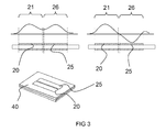
The natural modes of vibration (eigenmodes) of a pair of laterally-coupled BAW resonators will now be described, with reference to Fig. 3. A second BAW resonator is placed so close to the first resonator that one of its edges is within the exponentially decaying tail of the first resonator. The first and second resonators 21, 26 are defined by their corresponding electrodes 20, 25, respectively. The two resonators are said to be coupled: the system of two resonators has eigenmodes that are different from the eigenmodes of the individual resonators. For this LBAW system, the eigenmodes again consist of sinusoidal dependencies in the electrode areas 21 , 26 and exponential functions in the non-electrode region, decaying from the edge. In the gap between the resonators, exponentially decaying functions come from both sides. Given the boundary conditions at each interface between electrode and non-electrode regions, the eigenmodes can again be derived, but now for the system of coupled resonators. As before, each eigenmode has its associated eigenfrequency. Fig. 3 shows two eigenmodes of such an LBAW resonator consisting of two coupled resonators. The plots indicate the particle displacement associated with each eigenmode. Note that these two eigenmodes are fundamentally different from one another. In the first (shown on the left), the particles in the first resonator and second resonator vibrate in phase. In the second (shown on the right), they vibrate in anti-phase.
-
To find the eigenmodes of LBAW resonators, the formula used above for u
3(x,z) for a single isolated resonator can be extended. The only difference is that the number of regions increases. For two coupled resonators there are five regions: external regions to the left and right of the device; a gap region between the resonators; and the two electrode regions themselves. The eigenmode has the following shape:
For a two-resonator case, the mode shapes of the four lowest eigenmodes are shown in
Fig. 4.
-
In the foregoing description, the natural modes of vibration of isolated and coupled resonators, in the absence of external forces, were discussed. Now, the behaviour under external excitation will be considered. The mechanical response of the system under an external force can be described in terms of the eigenmodes derived above: the total vibration (that is, displacement) is a weighted sum of eigenmodes. The weight function for a particular eigenmode is a function of at two main factors. The first is the difference between the input or excitation frequency and the eigenfrequency of the eigenmode. The weight function is maximal when these frequencies are identical.
-
The second factor is the similarity between the x-dependence of the excitation force and the x-dependence of particle vibration amplitude for the given eigenmode: the weight function is proportional to the product of F(x) and u3(x), integrated over the electrode area. Here, F(x) is the excitation force and u3(x) the particle displacement for the eigenmode, both as a function of x. For example, if the excitation is uniform in x, and the eigenmodes are sinusoidal with odd and even dependence on x, then only the even modes are excited, because the product of F(x) with u3(x) for odd modes gives a zero integral. This applies to a stand-alone BAW resonator: the electric field (serving as the force F(x)) is uniform over the electrode area; therefore, only even modes are excited in response to an applied voltage.
-
In a coupled system, on the other hand, only the first resonator is excited and the second electrode reacts. Depending on the excitation frequency (compared to a nearby even or odd mode eigenfrequency) the system may exhibit either an even or an odd response. If the excitation frequency is equal to an even mode eigenfrequency, then the particle vibration in the second electrode is the same as the first electrode; in a pure odd mode response, the particle vibration has the same amplitude, but opposite sign (polarity). Not only are the amplitudes of particle vibration the same for both resonators, but also the amplitudes of voltage and current at the electrodes. In effect, at these frequencies, there is complete electrical signal transfer. From the perspective of filter-design, the eigenmodes which provide complete electrical signal transfer form the pass-band.
-
For frequencies distant from the eigenmode of the coupled resonator system, the even and odd eigenmodes are very weakly excited, and there is very little signal transfer. From the filter-design perspective, this translates to the desired out-of-band signal suppression.
-
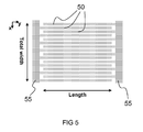
In the foregoing description, the behaviour of the resonators was modelled in a two-dimensional plane x-z. However, for a more complete understanding, it is necessary to consider the behaviour in three dimensions. This is especially relevant for coupled resonators with an interdigitated layout, as shown in Fig. 5. In the device illustrated in Fig. 5, each electrode comprises a plurality of fingers 50, of uniform width, connected to a busbar 55.
-
In the context of interdigitated electrodes, the two-dimensional modelling described above can be applied on a cross-section perpendicular to the finger length direction (that is, the xz-plane, with x as indicated in
Fig. 5 and z into the plane). It is often silently assumed that the wave function, representing acoustic and electrical behaviour, is uniform along the length direction. However, for conventional BAW resonators of rectangular shape, it is known that the eigenmodes have a sinusoidal dependence in both the x- and y-directions:
Here
Lx and
Ly are the edge lengths in the x and y direction, respectively, and m and n are integers. (m,n) is called the mode index. If Ly>>Lx, then the modes (
m,1) dominate the electrical device performance. For such conventional resonators, the fundamental mode (1,1) is the desired mode and the influence of the other modes (m,n) should be suppressed. For LBAWs, the three-dimensional eigenmodes can be expected to have the following shape
with
u3 (
x,z) as defined previously.
-
The current inventors have recognised that an LBAW device should be designed to trap at least two eigenmodes. In this regard, the laterally-coupled device contrasts with a conventional BAW device: for a conventional BAW device, trapping of one eigenmode is sufficient.
-
The reason for trapping a plurality of modes is to provide increased bandwidth: if an eigenmode is trapped and is effectively excited by an electrical signal on the input electrodes then, for excitation around the corresponding eigenfrequency, the system will vibrate according to the mode-shape of the eigenmode. If the output electrode also has effective coupling to this eigenmode, then the mode will attract charge. As a result, electrical signal transfer from the input to the output electrodes is possible for the full range of desired frequencies.
-
The modes that should be excited in the LBAW are the fundamental even mode and odd mode. The fundamental even mode is the (1,1)-mode: the wave function has one half sine in the width direction and one half sine in the length direction of the fingers. This mode is illustrated in the left-hand plot of Fig. 6. The fundamental odd mode for an M-finger device is the (M,1)-mode, with M half sines in the width direction and one in the length direction. This mode is illustrated in the right-hand plot in Fig. 6. The device of Fig. 6 is a nine-fingered coupled resonator; therefore, the fundamental odd mode is the (9,1)-mode. Overmodes are modes (m,n) with either m > M (overmodes in the width direction) or n>1 (overmodes in the length direction). The latter category, in particular, should not be excited as they will appear as peaks in the transmission curve of an LBAW filter. Overmodes in the length-direction for the nine-fingered device of Fig. 6 are shown in Fig. 7.
-
As is clear from the foregoing description, the successful implementation of filtering functionality using LBAW devices depends on careful selection of the eigenmodes which can be excited by an input signal. In the following description, a design methodology for correct trapping of eigenmodes will be discussed. In particular, the current inventors have recognised that careful design of the properties of the external region can be used to more accurately control the modes trapped.
-
According to an embodiment of the current invention, the external region is designed such that its cut-off frequency is just above the eigenfrequency of the highest eigenmode to be trapped. This ensures that exactly the desired modes are trapped. For LBAWs this provides a direct way of trapping the energy.
-
An example of this kind of energy trapping is shown in Fig. 8. The dispersion curve of the electrode region is shown by the dashed line. The eigenfrequencies of the fundamental even mode 60 and fundamental odd mode 62 are also shown, by horizontal lines on the graph. A sub-optimal dispersion curve for the external and gap regions is shown by the solid curve. This characteristic curve has a cut-off frequency that traps the even mode 60 but is too low to trap the odd mode 62. This will not give a good pass-band response - typically, the pass-band at the high-frequency side will show undesirably high insertion loss. The dotted curve shows another dispersion curve for the external region. This curve has been optimised by careful design of the layer stack, such that the cut-off frequency has been shifted upward by approximately 50 MHz. Now both the fundamental even and odd eigenmodes are trapped.
-
A similar approach can be used to control overmodes. Fig. 9 shows another set of example dispersion curves. Here the first (m,3)-mode, or overmode 64, is also shown. The sub-optimal curve (solid curve) for the external region has a cut-off frequency too high to reject this overmode. Trapping of overmodes typically gives rise to unwanted peaks in the frequency response, outside the pass-band. However, by optimisation of the layer stack in the external/gap regions, the dispersion can be adjusted to lower the cut-off frequency (as shown by the dotted curve). This latter curve provides trapping for the desired fundamental (both odd and even) eigenmodes, but suppresses the overmode 64.
-
To explain this approach in another way: the analysis, previously described above, has shown that for an eigenmode to be viable, the conditions for sinusoidal variation in the electrode region and exponential decay in the external region must be met. By modifying the construction (that is, layer stack) of the external region, the set of eigenmodes which can satisfy the exponential decay requirement is changed. This provides precise control of the trapped eigenmodes and thus precise control of the frequency characteristics of the coupled resonator system.
-
As discussed above, it is desirable to trap the fundamental odd and even eigenmodes, but reject all overmodes. Unfortunately, in some designs, this will not be possible, since the lowest overmode may have an eigenfrequency which is lower than that of the fundamental odd mode. That is, the desired modes and overmodes overlap, such that it is impossible to fully discriminate between them by selection of the cut-off frequency. It is nonetheless possible to predict (to a first approximation) the designs for which separation of the fundamental modes and overmodes is possible. This will be described in the following.
-
The desired fundamental odd mode in an M-finger device is the (M,1) mode. A lower limit for the wavelength associated with this fundamental odd mode, can be obtained by assuming the finger width
w finger to be equal to half of the lateral wavelength λ. In this case, assuming M>>1, the wave number is:
The lowest overmode in the length direction is the (1,3)-mode. The associated wave number can be approximated as:
Here,
width_total is the overall width of the LBAW device and L is the length of the fingers. For the dispersion curves considered above, the dispersion curve has a positive slope around the cut-off frequency. Therefore, the condition for separation of the fundamental modes and overmodes is
f eigen(1,3) >
f eigen(M,1); or equivalently,
k (1,3)>
k (M,1). So separation is possible if:
For a practical case, in which
width_total ≥
L, the first left-hand term will be dominated by the second term and the condition is thus:
This condition may or may not pose a limiting factor in practice, depending on other design considerations.
-
As described above, according to an embodiment of the invention, the dispersion of electrode region and external region are made different, in order to adapt the dispersion characteristics of the device. In particular the cut-off frequencies, f cutoff.electr and f cutoff.ext, are controlled independently. This means that the layer stacks for the two regions are different. Traditional ways of reducing the cut-off frequency of a given layer stack include: increasing the thickness of one or more layers; adding a layer (typically on top of the layer stack); or replacing one layer with another layer having a larger mass density or smaller acoustic wave velocity. Clearly, cut-off frequency can be increased by adopting the opposite strategies.
-
In this way, the principles for adjusting the cut-off frequency are similar to those for conventional BAW devices. Such principles will be well-known to the skilled person.
-
For example, when adding an additional layer, or increasing the thickness of an existing layer, the layer concerned may be on the top of the layer stack or deeper inside it. If the layer is at the top surface, its influence scales with the mass per unit area: that is, with ρt, where p is the mass density of the material and t is the layer thickness. Deeper in the layer stack, prediction of the effects is generally not this straightforward. Note that if the layer stack includes an acoustic reflector, then modification of layers within the reflector may be relatively ineffective: that is, the shift in cut-off frequency per nanometre of material is small.
-
In any case, given a desired shift in dispersion, the proper layer thickness can be derived from trial and error simulation. For this purpose, a simple one-dimensional simulation suffices. The principles of such a simulation have been described in, for example,
J. Rosenbaum, "Bulk Acoustic Wave Theory and Devices" (Artech House, Boston, MA, 1988) and are well-known.
-
One important but implicit difference between the layer stacks for external and electrode regions is that the latter has a bottom and top electrode. In the external region at least one of the electrode layers is missing, automatically making f cutoff.ext larger than f cutoff.electr. Thus, one approach to implementing the current invention is to carefully select the electrode layer material and its thickness, such that the cut-off frequency f cutoff.ext is just above the odd mode eigenfrequency of the system (for example, 2% above the eigenfrequency). In other words, the layer stack in the external region is designed to have the desired cut-off frequency. This layer stack is also shared by the electrode region; however, the cut-off frequency in this latter region can also be controlled by varying the thickness of the electrodes. This thickness can be chosen to provide the desired offset in cut-off frequencies between the electrode region and the external region. In this way, the electrode thickness in the electrode region can be said to indirectly provide the desired cut-off frequency in the external region.
-
In practice, an iterative design process may be employed. For example, the design of the layer stack for the electrode and external regions may be done as follows: a layer stack for the electrode region, consisting of at least a pair of electrodes and a piezoelectric layer, but usually also other layers (such as a reflector layer), is designed for good one-dimensional performance (proper cut-off frequency, negligible acoustic loss to the substrate, sufficient electromechanical coupling). Then, the properties - in particular the cut-off frequency - of the corresponding layer stack for the external region are investigated. Apart from the missing top electrode, this external region has the same stack as the electrode region. If the cut-off frequency is not within the desired range from the cut-off frequency of the electrode region (for example it is too high), the top electrode thickness is altered (thinned) and in order to maintain the same cut-off frequency for the electrode region, the thickness of one or more other layers is adapted (increased). In this new case, the adapted (thickened) other layer is shared by both the electrode and external regions. Therefore, the net effect is that the cut-off frequency of the external region is changed (lowered), while the cut-off frequency of the electrode region stays the same. This is a trial-and-error procedure that can be carried out with a conventional one-dimensional model.
-
There may be some circumstances in which control of the electrode material and thickness is insufficient to tune dispersion characteristics to the desired extent. For example, this design approach may lead to very thin electrodes, such that increased electrical resistance becomes a limiting factor in filter performance. Therefore, an alternative (or supplement) to this approach may be required. In another approach to implementation, electrodes are used that are thicker than would be suggested by the first method, but f cutoff.ext is decreased by adding a non-conducting layer to the external region.
-
Replacement of a given layer with a different material is also a technique well known to those skilled in the art. When this is done in the uppermost layer, the mass density is again the critical parameter. By way of example, a top electrode made of aluminium might be replaced by a layer of silicon dioxide in the external and/or gap regions. This approach is often more practical, as the freedom of the designer is not as restricted with regard to the thickness of the top electrode.
-
Note that the invention is not limited to these example approaches: as will be apparent to the skilled person, any method for controlling the dispersion of the electrode and/or external regions is within the scope of the invention.
-
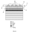
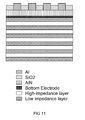
Fig. 10 shows an example according to an embodiment, combining several techniques to control dispersion (in particular, cut-off frequency). The device comprises a piezoelectric layer 10 formed of aluminium nitride and a bottom electrode 75 of platinum, beneath which lies a plurality of layers of silicon dioxide and tantalum pentoxide. The interdigitated top electrodes 50 are made of aluminium. In the gaps between the Al electrodes, SiO2 is deposited in layer 70. In this device, the layer stack of the gap and is identical to that of the external region. The thicknesses of the Al top electrode 50 and the SiO2 gap-filler 70 are chosen such that the difference in cut-off frequencies is approximately 100 MHz. In this example, the layer thickness 51 of the Al electrode is 455nm, while the thickness 71 of the silicon dioxide us 400 nm. As will be apparent to one skilled in the art, these value may be significantly different for other stack designs. Fig. 11 shows another, more general example of a layer stack design according to an embodiment.
-
Note that the foregoing description has considered resonator devices in which the layer stack exhibits so-called "Type-I" dispersion. Type-I dispersion curves have a positive slope for wave numbers about the cut-off frequency. However, other layer stacks exhibit "Type-II" dispersion, in which the dispersion curves have negative slope in the vicinity of the cut-off frequency. The invention is equally applicable to devices of this type. For Type-II dispersion, the basic condition is the same: that the wave number is imaginary-valued in the external region and real-valued in the electrode-region, for the eigenfrequencies to be trapped. However, due to the negative slope of the curve, this translates to a requirement that the cut-off frequency of the electrode region is above the desired eigenfrequencies while the cut-off frequency of the external region is below them.
-
Different approaches may be necessary for implementation of the invention in Type-II devices, as distinct from Type-I. For example, the external region may contain an extra layer, compared with the electrode region; one or more layers may be thicker in the external region than in the electrode region; or one or more layers in the external region have a higher mass density or smaller wave velocity than in the electrode region.
-
The implementation of layer stacks according to the principles of the invention can be achieved using known design tools. For example, the dispersion curves for a layer stack can be predicted from appropriate simulations, in one or two dimensions. Alternatively, the characteristics can be determined experimentally, for example by means of laser interferometry.
-
Although example LBAW devices according to embodiments of the first aspect of the invention have been described, it will be readily apparent to the skilled person that these examples do not imply limitations to the scope of application of the invention. For example, although interdigitated resonator structures have been described which have uniform finger-width, the invention is equally applicable to cases in which the widths of different fingers vary or the width of a given finger varies along its length. Similarly, the layer stacks of the gap (the portion between the electrodes) and the external or remaining portion (surrounding the electrodes and gap) may be the same or different.
-
The second aspect of the invention will now be described.
-
The current inventors have also recognised that the eigenmodes trapped and their mode-shapes can be influenced through independent control of the dispersion characteristics in the external portion as compared to the gap portion. Both these regions lack at least one of the two electrode layers; however, the current inventors have recognised that the layer stacks of the two regions can be made different, such that they no longer share the same dispersion characteristics.
-
This new degree of freedom can be exploited to design for a greater frequency difference between the first two fundamental eigenmodes, which has the effect of increasing the pass-band bandwidth of the filter transfer function.
-
Furthermore, is possible to design for real wave numbers in the gap regions, while the external region still presents an imaginary wave number at the eigenfrequencies of the eigenmodes of interest. Providing a real wave number in the gap region may also be helpful in realizing balun functionality. The benefits of providing an imaginary wave number in the external region have been discussed above in the context of the first aspect of the invention.
-
By choosing the cut-off frequencies of electrodes and gap to be identical (or nearly identical), the variation in the vertical mode-shape across the coupled resonators is minimized.
-
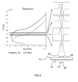
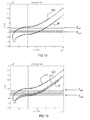
Examples of this aspect of the invention will now be described with reference to Figs. 12-16. Fig. 12 shows a set of simulated dispersion curves for a device not having the features of this aspect of the invention. In other words, the dispersion curves of Fig. 12 relate to a LBAW device in which the electrode region has dispersion characteristic E and the gap region and remaining (external) region has dispersion characteristic U1. The eigenfrequencies of the trapped eigenmodes are indicated by the solid horizontal lines. The lowest eigenfrequency (1901 MHz) corresponds to the fundamental even mode and the highest trapped eigenfrequency (1945MHz) corresponds to the fundamental odd eigenmode.
-
Fig. 13 shows a similar set of simulated dispersion curves, for a device according to an embodiment of the second aspect of the invention. That is, the electrode regions have dispersion characteristic E; the external (remaining) portion has dispersion U1; while the gap region between the electrodes has dispersion U2. The frequency difference between the corresponding highest (1940MHz) and lowest (1884MHz) trapped eigenmodes has been increased by approximately 25%. This means that the bandwidth provided by the filter is correspondingly increased. Note that the dispersion characteristics of the gap and the electrodes are nearly the same. Therefore, eigenmodes can be expected to exhibit a sinusoidal wave function in the gaps. At the same time, the dispersion of the remaining portion is preserved, so that this region presents an imaginary wave number. Thus, the eigenmode still exhibits an exponential wave function in this region, ensuring correct trapping.
-
Preferably, the cutoff frequency of the gap portion has a cutoff frequency within 2% of the corresponding cutoff frequency of the electrode portion.
-
The techniques that may be used to achieve the desired dispersion characteristics are similar to those discussed above in the context of the first aspect of the invention.
-
The dispersions of gap and external region must be made different. This means that the layer stacks for these two regions are different. Taking the layer stack of the remaining portion starting point, the task is to provide a gap region with lower cut-off frequency (assuming the device exhibits Type-I dispersion, as is the case for Figs. 12 and 13).
-
Ways of reducing the cut-off frequency of the layer stack include: increasing the thickness of one or more layers; or adding an extra layer, usually on top of the layer stack. For the non-electrode gap portion, any extra layer should preferably be of insulating material. In theory, it may be possible to use a metal, provided this is isolated from the electrodes; however, this would present practical problems, such as capacitive cross-talk with the electrodes.
-
The restriction that the extra layer is not a metal could be a substantial limitation for a conventional BAW device. In such devices, the layer stack design of the electrode region typically results in a relatively thick top electrode layer (for example, 100nm or more) with a high mass density (tungsten and platinum are commonly favoured materials). In many cases, impractically thick dielectrics would be required in order to bring the cut-off frequency for the gaps to a similar value as for the electrodes.
-
However, for LBAWs it is possible to avoid such thick and heavy electrodes. In one embodiment of the second aspect of the invention, a light metal (such as aluminium) is used for the top electrodes. The thickness of this electrode layer can be dictated by criteria other than acoustics - for example, the thickness can be chosen to provide a sufficiently low electrical resistance. The gaps between the electrodes can be filled (partially or completely) with a dielectric with mass density and thickness such that the cut-off frequencies of the gap region and the electrode region have the desired (small) frequency difference, as in Fig. 13. With a light metal such as aluminium, matching of cut-off frequencies can be achieved with reasonable thickness values of the dielectric material filling materials in the gap. There are no severe requirements for the dielectric material, apart from the fact that its intrinsic acoustic quality factor should be well above 1500: silicon dioxide, silicon nitride, and aluminium nitride all meet this requirement. It is preferable that the acoustic properties of the dielectric material are similar to those of the top electrode layer. This allows the design to use the same thickness of material in both regions, which can make the device easier to manufacture (see below).
-
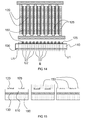
An example of a LBAW device according to such an embodiment is shown in Fig. 14. In this device, the first 120 and second 125 top electrodes have an interdigitated pattern. The top electrodes are laid on a layer of piezoelectric material 110, beneath which lies the bottom electrode 130. The gap between the first and second top electrodes is filled with a non-conducting material 150. The thickness of this is chosen to match the dispersion characteristic U2 of the gap region to the characteristic E of the electrode region. The external region has dispersion U1.
-
Chemical-Mechanical Polishing (CMP) may be beneficially employed to accurately control the thickness of the gap material. Accurate control is important since this thickness controls the frequency difference between the cut-off frequencies of the electrode and non-electrode regions. Figs. 15 and 16 Show examples of fabrication processes involving CMP.
-
As shown in the left-hand diagram of Fig. 15, top electrodes 120 and 125 are fabricated on top of the piezoelectric layer 110, beneath which lies the bottom electrode 130. In this example, the bottom electrode is located above a reflector layer 160. A layer of dielectric material 150 is deposited over the top electrodes 120 and 125 and exposed (non-electrode) portions of the piezoelectric layer 110. This step is shown in the middle diagram of Fig. 15. CMP is then performed, resulting in the layer structure shown in the right-hand diagram. In this case the dielectric in the gap region is intended to have the same thickness as the electrodes; therefore the top electrode material could conveniently serve as an etch-stop detector.
-
Fig. 16 shows a further example of a suitable set of processing steps. In this case, an additional sacrificial layer 170 is provided on top of the top electrodes 120 and 125. All other layers are as shown in Fig. 15. In this case, the sacrificial layer is used for etch-stop detection, therefore CMP stops when the top of this layer is exposed. Finally, the sacrificial layer is removed in a selective etch step, as shown in the far right-hand diagram of Fig. 16. In this way, the use of a sacrificial layer allows accurate control of the thickness of the dielectric in the gap region, even when the design calls for a thickness greater than that of the top electrodes. This allows greater flexibility and design freedom in the choice of materials and thicknesses.
-
As will be readily apparent to one skilled in the art, although the examples given above relate to Type-I devices, the second aspect of the invention is equally applicable to the design of LBAW devices having Type-II dispersion. In this case, of course, the conditions to be satisfied by the various cut-off frequencies will be reversed. For example: in the Type-I embodiment described above, it was noted that the cut-off frequency in the gap portion is reduced, compared to the cut-off frequency in the remaining portion. In an equivalent Type-II embodiment, the gap should have a higher cut-off frequency than the external region.
-
Although the example given in Fig. 14 relates to an interdigitated design, it will be equally clear to the skilled person that the second aspect of the invention is no less applicable to other electrode layouts.
-
The third aspect of the invention will now be described.
-
The current inventors have also recognised that the eigenmodes trapped and their mode-shapes and eigenfrequencies can be influenced by the careful design of electrode regions having spatially varying dispersion characteristics. More specifically: one (or more) of the electrode portions of the LBAW device can have a non-uniform layer structure. By way of example, we will consider two beneficial arrangements, which can be employed individually or combined. Both examples will be described in the context of the interdigitated electrode layout considered previously above. However, the skilled person will understand that the benefits of this aspect are not confined to such layouts.
-
In the first example, each finger of both electrode portions has a first segment at the finger-tip and a second segment, comprising the remainder of the length of the electrode, which has a different layer structure to the first segment. This is illustrated in Fig. 17. The first segment 222 at each finger tips has a dispersion characteristic with a lower cut-off frequency than the remainder of the finger (second segments 220). In the example shown in Fig. 17, the gap region 255 has the same layer structure (and therefore dispersion characteristic) as the external region surrounding the coupled resonators.
-
The variation in the dispersion characteristic at the finger tips has the effect of changing the shape of the eigenmodes supported by the device. In particular, the mode shape along the length direction of the fingers is changed, so that it is more uniform. Recalling Fig. 6, it can be seen that the fundamental odd and even modes obtained with a simple interdigitated layout have a sinusoidal profile (with a half-sine period) in the length direction. By providing finger ends with lower cut-off frequency (for Type-I devices), this sinusoidal mode-shape can be flattened and spread to present a more uniform profile over the length of each finger.
-
With this more uniform mode-shape, the coupling of the electric field to the fundamental eigenmodes is improved, because the electric field is itself uniform over the length of the finger. Accordingly, the quality factor of these modes is increased.
-
At the same time the suppression of unwanted higher modes can be improved. The shapes of the overmodes (m,n), where n is greater than 1, are modified so that they are sinusoids with a full wavelength over the length of the fingers. This is in contrast with Fig. 7, which shows overmodes with an odd number of half-sines. The excitation strength of the modified (full-wavelength) overmodes is very low.
-
Fig. 18 illustrates a variation on the layout of Fig. 17. Here, both the finger tips 222 and the adjacent segments 256 of the gap 255 have adapted dispersion characteristics (that is, adapted cut-off frequencies). The cut-off frequency of the first segments (finger tips 222) of the electrode portions is lower than that of the second segment (remainder 220). Similarly, the cut-off frequency of the first segments of the gap (gap-ends 256) is lower than that of the remainder of the gap 255. The cut-off frequencies of the electrode finger tips 222 and the gap-ends 256 may be the same.
-
Fig. 19 shows another variation. Compared with the example of Fig. 18, the dispersion characteristic of the gap region 250 is now modified with respect to the external region - that is, the remaining portion, surrounding the LBAW device. Therefore, this example combines this third aspect of the invention with the second aspect described previously above.
-
As can be seen from the examples of Figs. 17-19, independent control of the dispersion characteristics in the various regions provides multiple degrees of design-freedom. These can be used to optimise the device characteristics according to the needs of specific applications.
-
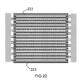
Fig. 20 presents a second example of the third aspect of the invention. This layout is similar to that of Fig. 19, but the outermost fingers in the interdigitated pattern are additionally provided with a longitudinal segment 223 which has a different dispersion characteristic to the rest of the fingers. The example of Fig. 20 includes the features described above, wherein the tips of the fingers also have modified dispersion characteristics. However, the longitudinal segments 223 on the outer fingers could also be provided independently of these other features. The longitudinal segments 223 may be partial width, or they may comprise the full width of the outermost fingers. According to the example shown in Fig. 20, the outer longitudinal segment 223 has a lower cut-off frequency than the remainder of the fingers 220. This corresponds to Type-I dispersion.
-
The effect of modifying the outermost fingers will now be described, with reference to Figs. 21 and 22. Firstly, note from Fig. 6 that the profile of the fundamental even eigenmode in the direction transverse to the finger length has a sinusoidal envelope, with one half-sine width. (This can be seen from the left-hand side of Fig, 6). The modification of the dispersion characteristic at the outside edge of the outermost fingers changes this.
-
The example of Fig. 21 assumes that the outer segments 223 of the electrode portions have a dispersion characteristic E2. The remaining, inner fingers 220 have dispersion E1. The gaps have dispersion U2, while the remaining portion (external region) has dispersion U1. The cut-off frequency of U1 is the highest, followed by U2, E1 and E2, in that order. The mode-shapes of the two fundamental modes are illustrated below the dispersion graph.
-
In the simulated example of Fig. 21, the separation between the even and odd eigenfrequencies is increased, compared with a case where all the electrode fingers are identical. This widens the pass-band bandwidth, in filter-design terms. The increased separation occurs because the modification of the outer fingers causes a reduction in the eigenfrequency of the lowest frequency (even) mode. This is also associated with a more nearly uniform wave-function across the interior fingers of the LBAW device (see the bottom plot of Fig. 21).
-
The example of Fig. 22 differs from Fig. 21 in that the dispersion E1of the inner fingers 220 has a higher cut-off frequency than the dispersion U2 of the gaps. This provides an even more uniform mode-shape. The eigenfrequency of the even eigenmode is even lower and so the separation of even and odd fundamental eiqenfrequencies is further increased.
-
These conditions on cut-off frequency apply to devices having Type-I dispersion. They can be re-stated more generally, in terms of the wave number, as follows. Referring to Fig. 21, for example, the dispersion characteristic E1 for the inner fingers presents a real-valued wave number at the eigenfrequencies of interest. For the external region, the characteristic U1 exhibits an imaginary wave number. This is as described previously for the first aspect of the invention. The corresponding wave numbers in the gap region are real (see U2) - to the extent that U2 matches E1. This is as described previously for the second aspect of the invention. The wave numbers of the modified outermost fingers are also real (see E2), but with values greater than either the inner electrodes or the gap region U2. This corresponds to a sinusoidal wave function with a shorter wavelength.
-
Modification of the outer edges of the electrode portions may be of particular benefit if the total width of the LBAW device is small. In an interdigitated layout, this may be because the number of fingers is low, or because the fingers and gaps are relatively narrow. The definition of "small" depends on the actual dispersion characteristics. In the context of the exemplary dispersion curves presented here, a total width of less than 30 microns can be considered small. However, where dispersion curves are steeper, wider devices than this may still be considered small.
-
As discussed already above, in the context of the first and second aspects of the invention, modification of the dispersion characteristic can be achieved by modifying the layer structure in the relevant portion of the LBAW device. The examples of Figs. 17-20 use a frame region, where either the finger tips; part of the outermost fingers; or both are adapted. For Type-I dispersion, the frame region should have a reduced cut-off frequency. This can be achieved, for example, by depositing an extra layer on top of the peripheral portions. Such a layer may be conducting or non-conducting. If it is conducting it may comprise part of the electrode. By now, it will be apparent to the skilled person that, to implement this aspect for Type-II dispersion, the cut-off frequency of the peripheral regions should instead be greater than that of the rest of the electrode fingers.
-
Those skilled in the art will recognise that, although they have been described separately, the features of the various aspects of the invention can be used together in embodiments, with beneficial effect.
-
Various other modifications will apparent to those skilled in the art.