EP2299427A1 - Driving System for Active-Matrix Displays - Google Patents
Driving System for Active-Matrix Displays Download PDFInfo
- Publication number
- EP2299427A1 EP2299427A1 EP20100175764 EP10175764A EP2299427A1 EP 2299427 A1 EP2299427 A1 EP 2299427A1 EP 20100175764 EP20100175764 EP 20100175764 EP 10175764 A EP10175764 A EP 10175764A EP 2299427 A1 EP2299427 A1 EP 2299427A1
- Authority
- EP
- European Patent Office
- Prior art keywords
- image data
- pixels
- grayscale image
- raw
- data
- Prior art date
- Legal status (The legal status is an assumption and is not a legal conclusion. Google has not performed a legal analysis and makes no representation as to the accuracy of the status listed.)
- Withdrawn
Links
Images


Classifications
-
- G—PHYSICS
- G09—EDUCATION; CRYPTOGRAPHY; DISPLAY; ADVERTISING; SEALS
- G09G—ARRANGEMENTS OR CIRCUITS FOR CONTROL OF INDICATING DEVICES USING STATIC MEANS TO PRESENT VARIABLE INFORMATION
- G09G3/00—Control arrangements or circuits, of interest only in connection with visual indicators other than cathode-ray tubes
- G09G3/20—Control arrangements or circuits, of interest only in connection with visual indicators other than cathode-ray tubes for presentation of an assembly of a number of characters, e.g. a page, by composing the assembly by combination of individual elements arranged in a matrix no fixed position being assigned to or needed to be assigned to the individual characters or partial characters
- G09G3/2007—Display of intermediate tones
- G09G3/2077—Display of intermediate tones by a combination of two or more gradation control methods
- G09G3/2081—Display of intermediate tones by a combination of two or more gradation control methods with combination of amplitude modulation and time modulation
-
- G—PHYSICS
- G09—EDUCATION; CRYPTOGRAPHY; DISPLAY; ADVERTISING; SEALS
- G09G—ARRANGEMENTS OR CIRCUITS FOR CONTROL OF INDICATING DEVICES USING STATIC MEANS TO PRESENT VARIABLE INFORMATION
- G09G3/00—Control arrangements or circuits, of interest only in connection with visual indicators other than cathode-ray tubes
- G09G3/20—Control arrangements or circuits, of interest only in connection with visual indicators other than cathode-ray tubes for presentation of an assembly of a number of characters, e.g. a page, by composing the assembly by combination of individual elements arranged in a matrix no fixed position being assigned to or needed to be assigned to the individual characters or partial characters
- G09G3/22—Control arrangements or circuits, of interest only in connection with visual indicators other than cathode-ray tubes for presentation of an assembly of a number of characters, e.g. a page, by composing the assembly by combination of individual elements arranged in a matrix no fixed position being assigned to or needed to be assigned to the individual characters or partial characters using controlled light sources
- G09G3/30—Control arrangements or circuits, of interest only in connection with visual indicators other than cathode-ray tubes for presentation of an assembly of a number of characters, e.g. a page, by composing the assembly by combination of individual elements arranged in a matrix no fixed position being assigned to or needed to be assigned to the individual characters or partial characters using controlled light sources using electroluminescent panels
- G09G3/32—Control arrangements or circuits, of interest only in connection with visual indicators other than cathode-ray tubes for presentation of an assembly of a number of characters, e.g. a page, by composing the assembly by combination of individual elements arranged in a matrix no fixed position being assigned to or needed to be assigned to the individual characters or partial characters using controlled light sources using electroluminescent panels semiconductive, e.g. using light-emitting diodes [LED]
- G09G3/3208—Control arrangements or circuits, of interest only in connection with visual indicators other than cathode-ray tubes for presentation of an assembly of a number of characters, e.g. a page, by composing the assembly by combination of individual elements arranged in a matrix no fixed position being assigned to or needed to be assigned to the individual characters or partial characters using controlled light sources using electroluminescent panels semiconductive, e.g. using light-emitting diodes [LED] organic, e.g. using organic light-emitting diodes [OLED]
- G09G3/3225—Control arrangements or circuits, of interest only in connection with visual indicators other than cathode-ray tubes for presentation of an assembly of a number of characters, e.g. a page, by composing the assembly by combination of individual elements arranged in a matrix no fixed position being assigned to or needed to be assigned to the individual characters or partial characters using controlled light sources using electroluminescent panels semiconductive, e.g. using light-emitting diodes [LED] organic, e.g. using organic light-emitting diodes [OLED] using an active matrix
-
- G—PHYSICS
- G09—EDUCATION; CRYPTOGRAPHY; DISPLAY; ADVERTISING; SEALS
- G09G—ARRANGEMENTS OR CIRCUITS FOR CONTROL OF INDICATING DEVICES USING STATIC MEANS TO PRESENT VARIABLE INFORMATION
- G09G2320/00—Control of display operating conditions
- G09G2320/02—Improving the quality of display appearance
- G09G2320/0271—Adjustment of the gradation levels within the range of the gradation scale, e.g. by redistribution or clipping
- G09G2320/0276—Adjustment of the gradation levels within the range of the gradation scale, e.g. by redistribution or clipping for the purpose of adaptation to the characteristics of a display device, i.e. gamma correction
-
- G—PHYSICS
- G09—EDUCATION; CRYPTOGRAPHY; DISPLAY; ADVERTISING; SEALS
- G09G—ARRANGEMENTS OR CIRCUITS FOR CONTROL OF INDICATING DEVICES USING STATIC MEANS TO PRESENT VARIABLE INFORMATION
- G09G2320/00—Control of display operating conditions
- G09G2320/04—Maintaining the quality of display appearance
- G09G2320/043—Preventing or counteracting the effects of ageing
-
- G—PHYSICS
- G09—EDUCATION; CRYPTOGRAPHY; DISPLAY; ADVERTISING; SEALS
- G09G—ARRANGEMENTS OR CIRCUITS FOR CONTROL OF INDICATING DEVICES USING STATIC MEANS TO PRESENT VARIABLE INFORMATION
- G09G2320/00—Control of display operating conditions
- G09G2320/06—Adjustment of display parameters
- G09G2320/0626—Adjustment of display parameters for control of overall brightness
-
- G—PHYSICS
- G09—EDUCATION; CRYPTOGRAPHY; DISPLAY; ADVERTISING; SEALS
- G09G—ARRANGEMENTS OR CIRCUITS FOR CONTROL OF INDICATING DEVICES USING STATIC MEANS TO PRESENT VARIABLE INFORMATION
- G09G2320/00—Control of display operating conditions
- G09G2320/06—Adjustment of display parameters
- G09G2320/0673—Adjustment of display parameters for control of gamma adjustment, e.g. selecting another gamma curve
-
- G—PHYSICS
- G09—EDUCATION; CRYPTOGRAPHY; DISPLAY; ADVERTISING; SEALS
- G09G—ARRANGEMENTS OR CIRCUITS FOR CONTROL OF INDICATING DEVICES USING STATIC MEANS TO PRESENT VARIABLE INFORMATION
- G09G2360/00—Aspects of the architecture of display systems
- G09G2360/14—Detecting light within display terminals, e.g. using a single or a plurality of photosensors
- G09G2360/144—Detecting light within display terminals, e.g. using a single or a plurality of photosensors the light being ambient light
-
- G—PHYSICS
- G09—EDUCATION; CRYPTOGRAPHY; DISPLAY; ADVERTISING; SEALS
- G09G—ARRANGEMENTS OR CIRCUITS FOR CONTROL OF INDICATING DEVICES USING STATIC MEANS TO PRESENT VARIABLE INFORMATION
- G09G2360/00—Aspects of the architecture of display systems
- G09G2360/16—Calculation or use of calculated indices related to luminance levels in display data
-
- G—PHYSICS
- G09—EDUCATION; CRYPTOGRAPHY; DISPLAY; ADVERTISING; SEALS
- G09G—ARRANGEMENTS OR CIRCUITS FOR CONTROL OF INDICATING DEVICES USING STATIC MEANS TO PRESENT VARIABLE INFORMATION
- G09G3/00—Control arrangements or circuits, of interest only in connection with visual indicators other than cathode-ray tubes
- G09G3/20—Control arrangements or circuits, of interest only in connection with visual indicators other than cathode-ray tubes for presentation of an assembly of a number of characters, e.g. a page, by composing the assembly by combination of individual elements arranged in a matrix no fixed position being assigned to or needed to be assigned to the individual characters or partial characters
- G09G3/2007—Display of intermediate tones
- G09G3/2018—Display of intermediate tones by time modulation using two or more time intervals
- G09G3/2022—Display of intermediate tones by time modulation using two or more time intervals using sub-frames
Definitions
- the present invention relates to display technology, and particularly to driving systems for active-matrix displays such as AMOLED displays.
- a display device having a plurality of pixels (or sub-pixels) arranged in a matrix has been widely used in various applications.
- Such a display device includes a panel having the pixels and peripheral circuits for controlling the panels.
- the pixels are defined by the intersections of scan lines and data lines, and the peripheral circuits include a gate driver for scanning the scan lines and a source driver for supplying image data to the data lines.
- the source driver may include a gamma correction circuit for controlling the gray scale of each pixel.
- the source driver and the gate driver respectively provide a data signal and a scan signal to the corresponding data line and the corresponding scan line. As a result, each pixel will display a predetermined brightness and color.
- OLED organic light emitting devices
- PDAs personal digital assistants
- the quality of output in an OLED based pixel is affected by the properties of a drive transistor that is typically fabricated from amorphous or poly silicon as well as the OLED itself.
- threshold voltage and mobility of the transistor tend to change as the pixel ages.
- the performance of the drive transistor may be effected by temperature. In order to maintain image quality, these parameters must be compensated for by adjusting the programming voltage to pixels.
- Compensation via changing the programming voltage is more effective when a higher level of programming voltage and therefore higher luminance is produced by the OLED based pixels.
- luminance levels are largely dictated by the level of brightness for the image data to a pixel, and the desired higher levels of luminance for more effective compensation may not be achievable while within the parameters of the image data.
- a system for using raw grayscale image data, representing images to be displayed in successive frames, to drive a display having pixels that include a drive transistor and an organic light emitting device.
- the system defines high and low ranges of raw grayscale image data, and determines whether the raw grayscale image data for each pixel falls within the high range or the low range.
- Raw grayscale image data that falls within the low range is converted to higher grayscale values, and the pixels are driven with currents corresponding to the higher grayscale values during time periods that are shorter than complete frame time periods.
- the high and low ranges may be selected according to how well the gamma curve corrects the raw grayscale image data within the ranges.
- a lookup table may be used to convert the grayscale image data that falls within the low range to higher grayscale values, and the higher grayscale values may contain an indicator that they have been converted from raw grayscale image data.
- the pixels are driven with currents corresponding to the raw grayscale image data that falls within the high range, during preselected time periods that are longer than the time periods during which the pixels are driven with currents corresponding to raw grayscale image data that falls within the low range.
- the preselected time periods may be shorter than a complete frame time period.
- Both the higher gray scale values converted from raw grayscale image data falling within the low range, and the raw grayscale image values falling within the high range may be gamma-corrected according to the same gamma correction curve.
- the system may include both a normal driving mode in which the pixels are driven with currents corresponding to the raw grayscale image data without converting any of the grayscale values to higher values, and a hybrid driving mode in which raw grayscale image data that falls within the low range is converted to higher grayscale values, and the pixels are driven with currents corresponding to said higher grayscale values during time periods that are shorter than a complete frame time period.
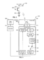
- FIG. 1 is a block diagram of an AMOLED display system.
- FIG. 2 is a block diagram of a pixel driver circuit for the AMOLED display in FIG. 1 .
- FIG. 3 is a block diagram similar to FIG. 1 but showing the source driver in more detail.
- FIG. 4A-4B are timing diagrams illustrating the time period of one complete frame and two sub-frame time periods within the complete frame time period.
- FIG. 5A-5D is a series of diagrammatic illustrations of the luminance produced by one pixel within the time periods of FIG. 4 in two different driving modes and when driven by two different grayscale values.
- FIG. 6 is a graph illustrating two different gamma curves, for use in two different driving modes, for different grayscale values.
- FIG. 7 is an illustration of exemplary values used to map grayscale data falling within a preselected low range to higher grayscale values.
- FIG. 8 is a diagrammatic illustration of the data used to drive any given pixel in the two sub-frame time periods illustrated in FIG. 4 , when the raw grayscale image data is in either of two different ranges.
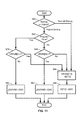
- FIG. 9 is a flow chart of a process executed by the source driver to convert raw grayscale image data that falls within a low range, to higher grayscale values.
- FIG. 10 is a flow chart of a process executed by the source driver to supply drive data to the pixels in either of two different operating modes.
- FIG. 11 is a flow chart of the same process illustrated in FIG. 10 with the addition of smoothing functions.
- FIG. 12 is a diagram illustrating the use of multiple lookup tables in the processing circuit in the source driver.
- FIG. 13 is a timing diagram of the programming signals sent to each row during a frame interval in the hybrid driving mode of the AMOLED display in FIG. 1 .
- FIG. 14A is a timing diagram for row and column drive signals showing programming and non-programming times for the hybrid drive mode using a single pulse.
- FIG. 14B is a timing diagram is a timing diagram for row and column drive signals showing programming and non-programming times for the hybrid drive mode using a double pulse.
- FIG. 15 is a diagram illustrating the use of multiple lookup tables and multiple gamma curves.
- FIG. 16A is a luminance level graph of the AMOLED display in FIG. 1 for automatic brightness control without hysteresis.
- FIG. 16B is a luminance level graph of the AMOLED display in FIG. 1 for automatic brightness control with hysteresis.
- FIG. 1 is an electronic display system 100 having an active matrix area or pixel array 102 in which an array of pixels 104 are arranged in a row and column configuration. For ease of illustration, only three rows and columns are shown.
- a peripheral area 106 External to the active matrix area of the pixel array 102 is a peripheral area 106 where peripheral circuitry for driving and controlling the pixel array 102 are disposed.
- the peripheral circuitry includes a gate or address driver circuit 108, a source or data driver circuit 110, a controller 112, and a supply voltage (e.g., Vdd) driver 114.
- the controller 112 controls the gate, source, and supply voltage drivers 108, 110, 114.
- the gate driver 108 under control of the controller 112, operates on address or select lines SEL[i], SEL[i+1], and so forth, one for each row of pixels 104 in the pixel array 102.
- a video source 120 feeds processed video data into the controller 112 for display on the display system 100.
- the video source 120 represents any video output from devices using the display system 100 such as a computer, cell phone, PDA and the like.
- the controller 112 converts the processed video data to the appropriate voltage programming information to the pixels 104 on the display system 100.
- the gate or address driver circuit 108 can also optionally operate on global select lines GSEL[j] and optionally /GSEL[j], which operate on multiple rows of pixels 104 in the pixel array 102, such as every three rows of pixels 104.
- the source driver circuit 110 under control of the controller 112, operates on voltage data lines Vdata[k], Vdata[k+1], and so forth, one for each column of pixels 104 in the pixel array 102.
- the voltage data lines carry voltage programming information to each pixel 104 indicative of a brightness (gray level) of each light emitting device in the pixel 104.
- a storage element, such as a capacitor, in each pixel 104 stores the voltage programming information until an emission or driving cycle turns on the light emitting device.
- the supply voltage driver 114 under control of the controller 112, controls the level of voltage on a supply voltage (EL_Vdd) line, one for each row of pixels 104 in the pixel array 102.
- the voltage driver 114 may individually control the level of supply voltage for each row of pixels 104 in the pixel array 102 or each column of pixels 104 in the pixel array 102.
- each pixel 104 in the display system 100 needs to be programmed with information indicating the brightness (gray level) of the organic light emitting device (OLED) in the pixel 104 for a particular frame.
- a frame defines the time period that includes a programming cycle or phase during which each and every pixel in the display system 100 is programmed with a programming voltage indicative of a brightness and a driving or emission cycle or phase during which each light emitting device in each pixel is turned on to emit light at a brightness commensurate with the programming voltage stored in a storage element.
- a frame is thus one of many still images that compose a complete moving picture displayed on the display system 100.
- There are at least two schemes for programming and driving the pixels row-by-row, or frame-by-frame.
- row-by-row programming a row of pixels is programmed and then driven before the next row of pixels is programmed and driven.
- frame-by-frame programming all rows of pixels in the display system 100 are programmed first, and all of the pixels are driven row-by-row. Either scheme can employ a brief vertical blanking time at the beginning or end of each frame during which the pixels are neither programmed nor driven.
- the components located outside of the pixel array 102 can be disposed in a peripheral area 106 around the pixel array 102 on the same physical substrate on which the pixel array 102 is disposed. These components include the gate driver 108, the source driver 110 and the supply voltage controller 114. Alternatively, some of the components in the peripheral area can be disposed on the same substrate as the pixel array 102 while other components are disposed on a different substrate, or all of the components in the peripheral are can be disposed on a substrate different from the substrate on which the pixel array 102 is disposed. Together, the gate driver 108, the source driver 110, and the supply voltage control 114 make up a display driver circuit. The display driver circuit in some configurations can include the gate driver 108 and the source driver 110 but not the supply voltage controller 114.
- the controller 112 includes internal memory (not shown) for various look up tabales and other data for functions such as compensation for effects such as temperature, change in threshold voltage, change in mobility, etc.
- the display system 100 allows the use of higher luminance of the pixels 104 during one part of the frame period while emitting not light in the other part of the frame period.
- the higher luminance during a limited time of the frame period results in the required brightness from the pixel for a frame but higher levels of luminance facilitate the compensation for changing parameters of the drive transistor performed by the controller 112.
- the system 100 also includes a light sensor 130 that is coupled to the controller 112.
- the light sensor 130 may be a single sensor located in proximity to the array 102 as in this example.
- the light sensor 130 may be multiple sensors such as one in each corner of the pixel array 102. Also, the light sensor 130 or multiple sensors may be embedded in the same substrate as the array 102, or have its own substrate on the array 102. As will be explained, the light sensor 130 allows adjustment of the overall brightness of the display system 100 according to ambient light conditions.
- FIG. 2 is a circuit diagram of a simple individual driver circuit 200 for a pixel such as the pixel 104 in FIG. 1 .
- the driver circuit 200 includes a drive transistor 202 coupled to an organic light emitting device (OLED) 204.
- OLED organic light emitting device
- the organic light emitting device 204 is fabricated from a luminous organic material which is activated by current flow and whose brightness is a function of the magnitude of the current.
- a supply voltage input 206 is coupled to the drain of the drive transistor 202. The supply voltage input 206 in conjunction with the drive transistor 202 creates current in the light emitting device 204.
- the current level may be controlled via a programming voltage input 208 coupled to the gate of the drive transistor 202.
- the programming voltage input 208 is therefore coupled to the source driver 110 in FIG. 1 .
- the drive transistor 202 is a thin film transistor fabricated from hydrogenated amorphous silicon.
- Other circuit components such as capacitors and transistors may be added to the simple driver circuit 200 to allow the pixel to operate with various enable, select and control signals such as those input by the gate driver 108 in FIG. 1 . Such components are used for faster programming of the pixels, holding the programming of the pixel during different frames, and other functions.
- the source driver 110 that supplies a data line voltage to a data line DL to program the selected pixels coupled to the data line DL.
- the controller 112 provides raw grayscale image data, at least one operation timing signal and a mode signal (hybrid or normal driving mode) to the source driver 110.
- Each of the gate driver 108 and the source driver 110 or a combination may be built from a one-chip semiconductor integrated circuit (IC) chip.
- the source driver 110 includes a timing interface (I/F) 342, a data interface (1/F) 324, a gamma correction circuit 340, a processing circuit 330, a memory 320 and a digital-to-analog converter (DAC) 322.
- the memory 320 is, for example, a graphic random access memory (GRAM) for storing grayscale image data.
- the DAC 322 includes a decoder for converting grayscale image data read from the GRAM 320 to a voltage corresponding to the luminance at which it is desired to have the pixels emit light.
- the DAC 322 may be a CMOS digital-to-analog converter.
- the source driver 110 receives raw grayscale image data via the data I/F 324, and a selector switch 326 determines whether the data is supplied directly to the GRAM 320, referred to as the normal mode, or to the processing circuit 330, referred to as the hybrid mode.
- the data supplied to the processing circuit 330 is converted from the typical 8-bit raw data to 9-bit hybrid data, e.g., by use of a hybrid Look-Up-Table (LUT) 332 stored in permanent memory which may be part of the processing circuit 330 or in a separate memory device such as ROM, EPROM, EEPROM, flash memory, etc.
- LUT Look-Up-Table
- the extra bit indicates whether each grayscale number is located in a predetermined low grayscale range LG or a predetermined high grayscale HG.
- the GRAM 320 supplies the DAC 322 with the raw 8-bit data in the normal driving mode and with the converted 9-bit data in the hybrid driving mode.
- the gamma correction circuit 340 supplies the DAC 322 with signals that indicate the desired gamma corrections to be executed by the DAC 322 as it converts the digital signals from the GRAM 320 to analog signals for the data lines DL. DACs that execute gamma corrections are well known in the display industry.
- the operation of the source driver 110 is controlled by one or more timing signals supplied to the gamma correction circuit 340 from the controller 112 through the timing I/F 342.
- the source driver 110 may be controlled to produce the same luminance according to the grayscale image data during an entire frame time T in the normal driving mode, and to produce different luminance levels during sub-frame time periods T1 and T2 in the hybrid driving mode to produce the same net luminance as in the normal driving mode.
- the processing circuit 330 converts or "maps" the raw grayscale data that is within a predetermined low grayscale range LG to a higher grayscale value so that pixels driven by data originating in either range are appropriately compensated to produce a uniform display during the frame time T.
- This compensation increases the luminance of pixels driven by data originating from raw grayscale image data in the low range LG, but the drive time of those pixels is reduced so that the average luminance of such pixels over the entire frame time T is at the desired level.
- the raw grayscale value is in a preselected high grayscale range HG, the pixel is driven to emit light during a major portion of the complete frame time period T, such as the portion 3 ⁇ 4T depicted in FIG. 5(c) .
- the pixel When the raw grayscale value is in the low range LG, the pixel is driven to emit light during a minor portion of the complete frame time period T, such as the portion 1 ⁇ 4T depicted in FIG. 5(d) , to reduce the frame time during which the increased voltage is applied.
- FIG. 6 illustrates an example in which raw grayscale values in a low range LG of 1-99 are mapped to corresponding values in a higher range of 102-245.
- one frame is divided into two sub-frame time periods T1 and T2.
- the duration of one full frame is T
- T2 (1/4)T.
- the value of ⁇ is not limited to 3/4 and may vary.
- raw grayscale data located in the low grayscale LG is transformed to high grayscale data for use in period T2.
- the operation timing of the sub-frame periods may be controlled by timing control signals supplied to the timing I/F 342.
- L1 represents the average luminance produced during a frame period T for raw grayscale data located in the high grayscale range HG, when the normal drive mode is selected.
- L3 represents the average luminance produced during a frame period T for raw grayscale data located in the low grayscale range LG, in the normal drive mode.
- L2 represents the average luminance for raw grayscale data located in the high grayscale range HG, during the sub-frame period T1 when the hybrid drive mode is selected.
- L4 represents the average luminance for raw grayscale data located in the low grayscale range LG, during the sub-frame period T2 when the hybrid drive mode is selected.
- the source driver 110 supplies the data line DL with a data line voltage corresponding to the black level ("0") in the sub-frame period T2. If the raw grayscale data is located in the high grayscale range HD, the source driver 110 supplies the data line DL with a data line voltage corresponding to the black level ("0") in the sub-frame period T1.
- FIG. 6 illustrates the gamma corrections executed by the DAC 322 in response to the control signals supplied to the DAC 322 by the gamma correction circuit 340.
- the source driver 110 uses a first gamma curve 4 for gamma correction in the hybrid driving mode, and a second gamma curve 6 for gamma correction in the normal driving mode.
- values in the low range LG are converted to higher grayscale values, and then both those converted values and the raw grayscale values that fall within the high range HG are gamma-corrected according to the same gamma curve 4.
- the gamma-corrected values are output from the DAC 322 to the data lines DL and used as the drive signals for the pixels 104, with the gamma-corrected high-range values driving their pixels in the first sub-frame time period T1, and the converted and gamma-corrected low-range values driving their pixels in the second sub-frame time period T2.
- the display system 100 divides the grayscales into a low grayscale range LG and a high grayscale range HG. Specifically, if the raw grayscale value of a pixel is greater than or equal to a reference value D(ref), that data is considered as the high grayscale range HG. If the raw grayscale value is smaller than the reference value D(ref), that data is considered as the low grayscale range LG.
- the reference value D(ref) is set to 100.
- the grayscale transformation is implemented by using the hybrid LUT 132 of FIG. 1 , as illustrated in FIGs. 6 and 7 .
- One example of the hybrid LUT 132 is shown in FIG. 7 where the grayscale values 1-99 in the low grayscale range LG are mapped to the grayscale values 102-245 in the high grayscale range HG.
- 8-bit grayscale data is provided for each color (e.g., R, G, B etc) and is used to drive the sub-pixels having those colors.
- the GRAM 320 stores the data in 9-bit words for the 8-bit grayscale data plus the extra bit added to indicate whether the 8-bit value is in the low or high grayscale range.
- data in the GRAM 320 is depicted as the nine bit word GRAM[8:0], with the bit GRAM[8] indicating whether the grayscale data is located in the high grayscale range HG or the low grayscale range LG.
- all the input data from the data I/F 124 is divided into two kinds of 8-bit grayscale data, as follows:
- FIG. 9 is a flow chart of one example of an operation for storing 8-bit grayscale data into the GRAM 320 as a 9-bit GRAM data word.
- the operation is implemented in the processing circuit 330 in the source driver 110.
- Raw grayscale data is input from the data I/F 124 at step 520, providing 8-bit data at step 522.
- the processing circuit 330 determines the system mode, i.e., normal driving mode or hybrid driving mode, at step 524. If the system mode is the hybrid driving mode, the system uses the 256*9 bit LUT 132 at step 528 to provide 9-bit data D_R[8:0] at step 530, including the one-bit range indicator. This data is stored in the GRAM 320 at step 532. If the system mode is the normal driving mode, the system uses the raw 8-bit input data D_N[7:0] at step 534, and stores the data in the GRAM 320 at step 532.
- FIG. 10 is a flow chart of one example of an operation for reading 9-bit GRAM data words and providing that data to the DAC 322.
- FIG. 11 is a flow chart of another example of an operation for reading 9-bit GRAM data and providing that data to the DAC 322.
- the routine of FIG. 11 uses a smoothing function for a different part of a frame.
- the smoothing function can be, but is not limited to, offset, shift or partial inversion.
- the step 552 of FIG. 10 is replaced with steps 560 and 562.
- GRAM[8] 1 (high range HG grayscale value)
- GRAM [7:0] is processed by the smoothing function f and then provided to the DAC 322 at step 560.
- GRAM[8] ⁇ 1 (low range LG grayscale value) GRAM [7:0] is processed by the smoothing function f and then provided to the DAC 322 at step 562.
- hybrid LUT 332 Although only one hybrid LUT 332 is illustrated in FIG. 3 , more than one hybrid LUT may be used, as illustrated in FIG. 12 .
- a plurality of hybrid LUTs 332 (1) ... 332 (m) receive data from, and have outputs coupled to, a multiplexer 350. Different ranges of grayscale values can be converted in different hybrid LUTs.
- FIG. 13 is a timing diagram of the programming signals sent to each row during a frame interval in the hybrid driving mode of the AMOLED display in FIG. 1 and FIG. 3 .
- Each frame is assigned a time interval such as the time intervals 600, 602, and 604, which is sufficient to program each row in the display.
- the display has 480 rows.
- Each of the 480 rows include pixels for corresponding image data that may be in the low grayscale value range or the high grayscale value range.
- each of the time intervals 600, 602, and 604 represent 60 frames per second or a frequency of 60 Hz. Of course other higher and lower frequencies and different numbers of rows may be used with the hybrid driving mode.
- the timing diagram in FIG. 13 includes control signals necessary to avoid a tearing effect where programming data for the high and low grayscale values may overlap.
- the control signals include a tearing signal line 610, a data write signal line 612, a memory out low value (R) signal line 614 and a memory out high value (P) signal line 616.
- the hybrid driving mode is initiated for each frame by enabling the tearing signal line 610.
- the data write signal line 612 receives the row programming data 620 for each of the rows in the display system 100.
- the programming data 620 is processed using the LUTs as described above to convert the data to analog values reflecting higher luminance values for shortened intervals for each of the pixels in each row.
- a blanking interval 622 and a blanking interval 630 represent no output through the memory write lines 614 and 616 respectively.
- a row programming data block 624 is output from the memory out low value line 614.
- the row programming data block 624 includes programming data for all pixels in each row in succession beginning with row 1.
- the row programming data block 624 includes only data for the pixels in the selected row that are to be driven at values in the low grayscale range. As explained above, all pixels that are to be driven at values in the high grayscale range in a selected row are set to zero voltage or adjusted for distortions.
- the DAC 322 converts the low gray scale range data (for pixels programmed in the low grayscale range) and sends the programming signals to the pixels (LUT modified data for the low grayscale range pixels and a zero voltage or distortion adjustment for the high grayscale range pixels) in that row.
- the row programming data block 634 includes programming data for all pixels in each row in succession beginning with row 1.
- the row programming data block 634 includes only data for the pixels that are to be driven at values in the high grayscale range in the selected row. As explained above, all pixels that are to be driven at values in the low grayscale range in the selected row are set to zero voltage.
- the DAC 322 converts the high gray scale range data (for pixels programmed in the high grayscale range) and sends the programming signals to the pixels (LUT modified data for the high grayscale range pixels and a zero voltage for the low grayscale range pixels) in that row.
- the delay period 632 is set to 1F+x/3 where F is the time it takes to program all 480 rows and x is the time of the blanking intervals 622 and 630.
- the x variable may be defined by the manufacturer based on the speed of the components such as the processing circuit 330 necessary to eliminate tearing. Therefore, x may be lower for faster processing components.
- the delay period 632 between programming pixels emitting a level in the low grayscale range and those pixels emitting a level in the high grayscale range avoids the tearing effect.
- FIG. 14A is a timing diagram for row and column drive signals showing programming and non-programming times for the hybrid drive mode using a single pulse for the AMOLED display in FIG. 1 .
- the diagram in FIG. 14A includes a tearing signal 640, a set of programming voltage select signals 642, a gate clock signal 644, and row strobe signals 646a-646h.
- the tearing signal 640 is strobed low to initiate the hybrid drive mode for a particular video frame.
- the programming voltage select signals 642 allow the selection of all of the pixels in a particular row for receiving programming voltages from the DAC 322 in FIG. 3 . In this example, there are 960 pixels in each row.
- the programming voltage select signals 642 initially are selected to send a set of low grayscale range programming voltages 650 to the pixels of the first row.
- the strobe signal 646a for the first row produces a pulse 652 to select the row.
- the low gray scale pixels in that row are then driven by the programming voltages from the DAC 322 while the high grayscale pixels are driven to zero voltage.
- the programming voltage select signals 642 are selected to send a set of high grayscale range programming voltages 654 to the first row.
- the strobe signal 646a for the first row produces a second pulse 656 to select the row.
- the high grayscale pixels in that row are then driven by the programming voltages from the DAC 322 while the low grayscale pixels are driven to zero voltage.
- this process is repeated for each of the rows via the row strobe signals 646b-646g.
- Each row is therefore strobed twice, once for programming the low grayscale pixels and once for programming the high grayscale values.
- FIG. 14B is a timing diagram for row and column drive signals showing programming and non-programming times for the hybrid drive mode using a double pulse.
- the double pulse to the drive circuit of the next row leaves the leakage path on for the drive transistor and helps improve compensation for the drive transistors.
- the diagram in FIG. 14B includes a tearing signal 680, a set of programming voltage select signals 682, a gate clock signal 684, and row strobe signals 686a-686h.
- the tearing signal 680 is strobed low to initiate the hybrid drive mode for a particular video frame.
- the programming voltage select signals 682 allow the selection of all of the pixels in a particular row for receiving programming voltages from the DAC 322 in FIG. 3 .
- the programming voltage select signals 682 initially are selected to send a set of low grayscale range programming voltages 690 to the first row.
- the strobe signal 686a for the first row produces a pulse 692 to select the row.
- the low gray scale pixels in that row are then driven by the programming voltages from the DAC 322 while the high grayscale pixels are driven to zero voltage.
- the programming voltage select signals 682 are selected to send a set of high grayscale range programming voltages 694 to the first row.
- the gate clock signal 684 is set high, the strobe signal 686a for the first row produces a second pulse 696 to select the row.
- the high grayscale pixels in that row are then driven by the programming voltages from the DAC 322 while the low grayscale pixels are driven to zero voltage.
- this process is repeated for each of the rows via the row strobe signals 686b-686g.
- Each row is therefore strobed once for programming the low grayscale pixels and once for programming the high grayscale values.
- Each row is also strobed simultaneously with the previous row, such as the high strobe pulses 692 on the row strobe line 686a and 686b, in order to leave the leakage path on for the drive transistor.
- the last strobe line 686h is a dummy line that is strobed for the purpose of leaving the leakage path on for the drive transistor for the last active row in the display.
- FIG. 15 illustrates a system implementation for accommodating multiple gamma curves for different applications and automatic brightness control, using the hybrid driving scheme.
- the automatic brightness control is feature where the controller 112 adjusts the overall luminance level of the display system 100 according to the level of ambient light detected by the light sensor 130 in FIG. 1 .
- the display system 100 may have four levels of brightness: bright, normal, dim and dimmest. Of course any number of levels of brightness may be used.
- a different set of voltages from LUTs 700 (#1-#n) is provided to a plurality of DAC decoders 322a in the source driver 110.
- the set of voltages is used to change the display peak brightness using the different sets of voltages 700.
- Multiple gamma LUTs 702 (#1-#m) are provided so that the DACs 322a can also change the voltages from the hybrid LUTs 700 to obtain a more solid gamma curve despite changing the peak brightness.
- gamma 2.2 bright, gamma 2.2 normal, gamma 2.2 dim, gamma 1.0, gamma 1.8 and gamma 2.5 there are 18 conditions with corresponding 18 gamma curve LUTs stored in a memory of the gamma correction circuit 340 in FIG. 3 .
- Three gamma conditions, gamma 2.2 bright, gamma 2.2 normal and gamma 2.2 dim, are used according to the brightness level. In this example, the dim and dimmest brightness levels both use the gamma 2.2 dim condition.
- the other gamma conditions are used for application specific requirements.
- Each of the six gamma conditions for each color have their own gamma curve LUTs 702 in FIG.
- FIG. 16A and 16B show graphs of two modes of the brightness control that may be implemented by the controller 112.
- FIG. 16A shows the brightness control without hysteresis.
- the y-axis of the graph 720 shows the four levels of overall luminance of the display system 100.
- the luminance levels include a bright level 722, a normal level 724, a dim level 726 and a dimmest level 728.
- the x-axis of the graph 720 represents the output of the light sensor 130.
- the x-axis shows a low level 730, a middle level 732 and a high level 734.
- the luminance level is adjusted downward or upward to the next level using the LUTs 700 in FIG. 15 .
- the luminance of the display is adjusted up to the normal level 724. If ambient light is reduced below the low level 730, the luminance of the display is adjusted down to the dimmest level 728.
- FIG. 16B is a graph 750 showing the brightness control of the display system 100 in hysteresis mode.
- the brightness levels are sustained for a longer period when transitions are made between luminance levels.
- the y-axis of the graph 750 shows the four levels of overall luminance of the display system 100.
- the levels include a bright level 752, a normal level 754, a dim level 756 and a dimmest level 758.
- the x-axis of the graph 750 represents the output of the light sensor 130. Thus, as the output increases past certain threshold levels, indicating greater levels of ambient light, the luminance of the display system 100 is increased.
- the x-axis shows a low base level 760, a middle base level 762 and a high level 764.
- Each level 760, 762 and 764 includes a corresponding increase threshold level 770, 772 and 774 and a corresponding decrease threshold level 780, 782 and 784.
- Increases in luminance require greater ambient light than the base levels 760, 762 and 764. For example, when the ambient light detected exceeds an increase threshold level such as the threshold level 770, the luminance of the display is adjusted up to the dim level 756. Decreases in luminance require less ambient light than the base levels 760, 762 and 764. For example, if ambient light is reduced below the decrease threshold level 794, the luminance of the display is adjusted down to the normal level 754.
Landscapes
- Engineering & Computer Science (AREA)
- Physics & Mathematics (AREA)
- Computer Hardware Design (AREA)
- General Physics & Mathematics (AREA)
- Theoretical Computer Science (AREA)
- Control Of Indicators Other Than Cathode Ray Tubes (AREA)
- Electroluminescent Light Sources (AREA)
- Control Of El Displays (AREA)
Abstract
Description
- The present invention relates to display technology, and particularly to driving systems for active-matrix displays such as AMOLED displays.
- A display device having a plurality of pixels (or sub-pixels) arranged in a matrix has been widely used in various applications. Such a display device includes a panel having the pixels and peripheral circuits for controlling the panels. Typically, the pixels are defined by the intersections of scan lines and data lines, and the peripheral circuits include a gate driver for scanning the scan lines and a source driver for supplying image data to the data lines. The source driver may include a gamma correction circuit for controlling the gray scale of each pixel. In order to display a frame, the source driver and the gate driver respectively provide a data signal and a scan signal to the corresponding data line and the corresponding scan line. As a result, each pixel will display a predetermined brightness and color.
- In recent years, the matrix display using organic light emitting devices (OLED) has been widely employed in small electronic devices, such as handheld devices, cellular phones, personal digital assistants (PDAs), and cameras because of the generally lower power consumed by such devices. However, the quality of output in an OLED based pixel is affected by the properties of a drive transistor that is typically fabricated from amorphous or poly silicon as well as the OLED itself. In particular, threshold voltage and mobility of the transistor tend to change as the pixel ages. Moreover, the performance of the drive transistor may be effected by temperature. In order to maintain image quality, these parameters must be compensated for by adjusting the programming voltage to pixels. Compensation via changing the programming voltage is more effective when a higher level of programming voltage and therefore higher luminance is produced by the OLED based pixels. However, luminance levels are largely dictated by the level of brightness for the image data to a pixel, and the desired higher levels of luminance for more effective compensation may not be achievable while within the parameters of the image data.
- According to one embodiment, a system is provided for using raw grayscale image data, representing images to be displayed in successive frames, to drive a display having pixels that include a drive transistor and an organic light emitting device. The system defines high and low ranges of raw grayscale image data, and determines whether the raw grayscale image data for each pixel falls within the high range or the low range. Raw grayscale image data that falls within the low range is converted to higher grayscale values, and the pixels are driven with currents corresponding to the higher grayscale values during time periods that are shorter than complete frame time periods. When the raw grayscale image data is adjusted according to a preselected gamma curve before using that data to drive the pixels, the high and low ranges may be selected according to how well the gamma curve corrects the raw grayscale image data within the ranges. A lookup table may be used to convert the grayscale image data that falls within the low range to higher grayscale values, and the higher grayscale values may contain an indicator that they have been converted from raw grayscale image data.
- In one implementation, the pixels are driven with currents corresponding to the raw grayscale image data that falls within the high range, during preselected time periods that are longer than the time periods during which the pixels are driven with currents corresponding to raw grayscale image data that falls within the low range. The preselected time periods may be shorter than a complete frame time period. Both the higher gray scale values converted from raw grayscale image data falling within the low range, and the raw grayscale image values falling within the high range, may be gamma-corrected according to the same gamma correction curve.
- The system may include both a normal driving mode in which the pixels are driven with currents corresponding to the raw grayscale image data without converting any of the grayscale values to higher values, and a hybrid driving mode in which raw grayscale image data that falls within the low range is converted to higher grayscale values, and the pixels are driven with currents corresponding to said higher grayscale values during time periods that are shorter than a complete frame time period.
- The foregoing and additional aspects and embodiments of the present invention will be apparent to those of ordinary skill in the art in view of the detailed description of various embodiments and/or aspects, which is made with reference to the drawings, a brief description of which is provided next.
- The foregoing and other advantages of the invention will become apparent upon reading the following detailed description and upon reference to the drawings.
-
FIG. 1 is a block diagram of an AMOLED display system. -
FIG. 2 is a block diagram of a pixel driver circuit for the AMOLED display inFIG. 1 . -
FIG. 3 is a block diagram similar toFIG. 1 but showing the source driver in more detail. -
FIG. 4A-4B are timing diagrams illustrating the time period of one complete frame and two sub-frame time periods within the complete frame time period. -
FIG. 5A-5D is a series of diagrammatic illustrations of the luminance produced by one pixel within the time periods ofFIG. 4 in two different driving modes and when driven by two different grayscale values. -
FIG. 6 is a graph illustrating two different gamma curves, for use in two different driving modes, for different grayscale values. -
FIG. 7 is an illustration of exemplary values used to map grayscale data falling within a preselected low range to higher grayscale values. -
FIG. 8 is a diagrammatic illustration of the data used to drive any given pixel in the two sub-frame time periods illustrated inFIG. 4 , when the raw grayscale image data is in either of two different ranges. -
FIG. 9 is a flow chart of a process executed by the source driver to convert raw grayscale image data that falls within a low range, to higher grayscale values. -
FIG. 10 is a flow chart of a process executed by the source driver to supply drive data to the pixels in either of two different operating modes. -
FIG. 11 is a flow chart of the same process illustrated inFIG. 10 with the addition of smoothing functions. -
FIG. 12 is a diagram illustrating the use of multiple lookup tables in the processing circuit in the source driver. -
FIG. 13 is a timing diagram of the programming signals sent to each row during a frame interval in the hybrid driving mode of the AMOLED display inFIG. 1 . -
FIG. 14A is a timing diagram for row and column drive signals showing programming and non-programming times for the hybrid drive mode using a single pulse. -
FIG. 14B is a timing diagram is a timing diagram for row and column drive signals showing programming and non-programming times for the hybrid drive mode using a double pulse. -
FIG. 15 is a diagram illustrating the use of multiple lookup tables and multiple gamma curves. -
FIG. 16A is a luminance level graph of the AMOLED display inFIG. 1 for automatic brightness control without hysteresis. -
FIG. 16B is a luminance level graph of the AMOLED display inFIG. 1 for automatic brightness control with hysteresis. - While the invention is susceptible to various modifications and alternative forms, specific embodiments have been shown by way of example in the drawings and will be described in detail herein. It should be understood, however, that the invention is not intended to be limited to the particular forms disclosed. Rather, the invention is to cover all modifications, equivalents, and alternatives falling within the spirit and scope of the invention as defined by the appended claims.
-
FIG. 1 is anelectronic display system 100 having an active matrix area orpixel array 102 in which an array ofpixels 104 are arranged in a row and column configuration. For ease of illustration, only three rows and columns are shown. External to the active matrix area of thepixel array 102 is aperipheral area 106 where peripheral circuitry for driving and controlling thepixel array 102 are disposed. The peripheral circuitry includes a gate oraddress driver circuit 108, a source ordata driver circuit 110, acontroller 112, and a supply voltage (e.g., Vdd)driver 114. Thecontroller 112 controls the gate, source, andsupply voltage drivers gate driver 108, under control of thecontroller 112, operates on address or select lines SEL[i], SEL[i+1], and so forth, one for each row ofpixels 104 in thepixel array 102. Avideo source 120 feeds processed video data into thecontroller 112 for display on thedisplay system 100. Thevideo source 120 represents any video output from devices using thedisplay system 100 such as a computer, cell phone, PDA and the like. Thecontroller 112 converts the processed video data to the appropriate voltage programming information to thepixels 104 on thedisplay system 100. - In pixel sharing configurations described below, the gate or
address driver circuit 108 can also optionally operate on global select lines GSEL[j] and optionally /GSEL[j], which operate on multiple rows ofpixels 104 in thepixel array 102, such as every three rows ofpixels 104. Thesource driver circuit 110, under control of thecontroller 112, operates on voltage data lines Vdata[k], Vdata[k+1], and so forth, one for each column ofpixels 104 in thepixel array 102. The voltage data lines carry voltage programming information to eachpixel 104 indicative of a brightness (gray level) of each light emitting device in thepixel 104. A storage element, such as a capacitor, in eachpixel 104 stores the voltage programming information until an emission or driving cycle turns on the light emitting device. Thesupply voltage driver 114, under control of thecontroller 112, controls the level of voltage on a supply voltage (EL_Vdd) line, one for each row ofpixels 104 in thepixel array 102. Alternatively, thevoltage driver 114 may individually control the level of supply voltage for each row ofpixels 104 in thepixel array 102 or each column ofpixels 104 in thepixel array 102. - As is known, each
pixel 104 in thedisplay system 100 needs to be programmed with information indicating the brightness (gray level) of the organic light emitting device (OLED) in thepixel 104 for a particular frame. A frame defines the time period that includes a programming cycle or phase during which each and every pixel in thedisplay system 100 is programmed with a programming voltage indicative of a brightness and a driving or emission cycle or phase during which each light emitting device in each pixel is turned on to emit light at a brightness commensurate with the programming voltage stored in a storage element. A frame is thus one of many still images that compose a complete moving picture displayed on thedisplay system 100. There are at least two schemes for programming and driving the pixels: row-by-row, or frame-by-frame. In row-by-row programming, a row of pixels is programmed and then driven before the next row of pixels is programmed and driven. In frame-by-frame programming, all rows of pixels in thedisplay system 100 are programmed first, and all of the pixels are driven row-by-row. Either scheme can employ a brief vertical blanking time at the beginning or end of each frame during which the pixels are neither programmed nor driven. - The components located outside of the
pixel array 102 can be disposed in aperipheral area 106 around thepixel array 102 on the same physical substrate on which thepixel array 102 is disposed. These components include thegate driver 108, thesource driver 110 and thesupply voltage controller 114. Alternatively, some of the components in the peripheral area can be disposed on the same substrate as thepixel array 102 while other components are disposed on a different substrate, or all of the components in the peripheral are can be disposed on a substrate different from the substrate on which thepixel array 102 is disposed. Together, thegate driver 108, thesource driver 110, and thesupply voltage control 114 make up a display driver circuit. The display driver circuit in some configurations can include thegate driver 108 and thesource driver 110 but not thesupply voltage controller 114. - The
controller 112 includes internal memory (not shown) for various look up tabales and other data for functions such as compensation for effects such as temperature, change in threshold voltage, change in mobility, etc. Unlike a convention AMOLED, thedisplay system 100 allows the use of higher luminance of thepixels 104 during one part of the frame period while emitting not light in the other part of the frame period. The higher luminance during a limited time of the frame period results in the required brightness from the pixel for a frame but higher levels of luminance facilitate the compensation for changing parameters of the drive transistor performed by thecontroller 112. Thesystem 100 also includes a light sensor 130 that is coupled to thecontroller 112. The light sensor 130 may be a single sensor located in proximity to thearray 102 as in this example. Alternatively, the light sensor 130 may be multiple sensors such as one in each corner of thepixel array 102. Also, the light sensor 130 or multiple sensors may be embedded in the same substrate as thearray 102, or have its own substrate on thearray 102. As will be explained, the light sensor 130 allows adjustment of the overall brightness of thedisplay system 100 according to ambient light conditions. -
FIG. 2 is a circuit diagram of a simpleindividual driver circuit 200 for a pixel such as thepixel 104 inFIG. 1 . As explained above, eachpixel 104 in thepixel array 102 inFIG. 1 is driven by thedriver circuit 200 inFIG. 2 . Thedriver circuit 200 includes adrive transistor 202 coupled to an organic light emitting device (OLED) 204. In this example, the organiclight emitting device 204 is fabricated from a luminous organic material which is activated by current flow and whose brightness is a function of the magnitude of the current. Asupply voltage input 206 is coupled to the drain of thedrive transistor 202. Thesupply voltage input 206 in conjunction with thedrive transistor 202 creates current in thelight emitting device 204. The current level may be controlled via a programming voltage input 208 coupled to the gate of thedrive transistor 202. The programming voltage input 208 is therefore coupled to thesource driver 110 inFIG. 1 . In this example, thedrive transistor 202 is a thin film transistor fabricated from hydrogenated amorphous silicon. Other circuit components (not shown) such as capacitors and transistors may be added to thesimple driver circuit 200 to allow the pixel to operate with various enable, select and control signals such as those input by thegate driver 108 inFIG. 1 . Such components are used for faster programming of the pixels, holding the programming of the pixel during different frames, and other functions. - Referring to
FIG. 3 , there is illustrated thesource driver 110 that supplies a data line voltage to a data line DL to program the selected pixels coupled to the data line DL. Thecontroller 112 provides raw grayscale image data, at least one operation timing signal and a mode signal (hybrid or normal driving mode) to thesource driver 110. Each of thegate driver 108 and thesource driver 110 or a combination may be built from a one-chip semiconductor integrated circuit (IC) chip. - The
source driver 110 includes a timing interface (I/F) 342, a data interface (1/F) 324, agamma correction circuit 340, aprocessing circuit 330, amemory 320 and a digital-to-analog converter (DAC) 322. Thememory 320 is, for example, a graphic random access memory (GRAM) for storing grayscale image data. TheDAC 322 includes a decoder for converting grayscale image data read from theGRAM 320 to a voltage corresponding to the luminance at which it is desired to have the pixels emit light. TheDAC 322 may be a CMOS digital-to-analog converter. - The
source driver 110 receives raw grayscale image data via the data I/F 324, and a selector switch 326 determines whether the data is supplied directly to theGRAM 320, referred to as the normal mode, or to theprocessing circuit 330, referred to as the hybrid mode. The data supplied to theprocessing circuit 330 is converted from the typical 8-bit raw data to 9-bit hybrid data, e.g., by use of a hybrid Look-Up-Table (LUT) 332 stored in permanent memory which may be part of theprocessing circuit 330 or in a separate memory device such as ROM, EPROM, EEPROM, flash memory, etc. The extra bit indicates whether each grayscale number is located in a predetermined low grayscale range LG or a predetermined high grayscale HG. - The
GRAM 320 supplies theDAC 322 with the raw 8-bit data in the normal driving mode and with the converted 9-bit data in the hybrid driving mode. Thegamma correction circuit 340 supplies theDAC 322 with signals that indicate the desired gamma corrections to be executed by theDAC 322 as it converts the digital signals from theGRAM 320 to analog signals for the data lines DL. DACs that execute gamma corrections are well known in the display industry. - The operation of the
source driver 110 is controlled by one or more timing signals supplied to thegamma correction circuit 340 from thecontroller 112 through the timing I/F 342. For example, thesource driver 110 may be controlled to produce the same luminance according to the grayscale image data during an entire frame time T in the normal driving mode, and to produce different luminance levels during sub-frame time periods T1 and T2 in the hybrid driving mode to produce the same net luminance as in the normal driving mode. - In the hybrid driving mode, the
processing circuit 330 converts or "maps" the raw grayscale data that is within a predetermined low grayscale range LG to a higher grayscale value so that pixels driven by data originating in either range are appropriately compensated to produce a uniform display during the frame time T. This compensation increases the luminance of pixels driven by data originating from raw grayscale image data in the low range LG, but the drive time of those pixels is reduced so that the average luminance of such pixels over the entire frame time T is at the desired level. Specifically, when the raw grayscale value is in a preselected high grayscale range HG, the pixel is driven to emit light during a major portion of the complete frame time period T, such as the portion ¾T depicted inFIG. 5(c) . When the raw grayscale value is in the low range LG, the pixel is driven to emit light during a minor portion of the complete frame time period T, such as the portion ¼T depicted inFIG. 5(d) , to reduce the frame time during which the increased voltage is applied. -
FIG. 6 illustrates an example in which raw grayscale values in a low range LG of 1-99 are mapped to corresponding values in a higher range of 102-245. In the hybrid driving mode, one frame is divided into two sub-frame time periods T1 and T2. The duration of one full frame is T, the duration of one sub-frame time period is T1 = αT, and the duration of the other sub-frame time period is T2 = (1-α)T, so T = T1+T2. In the example inFIG. 5 , α = 3/4, and thus T1 = (3/4)T, and T2 = (1/4)T. The value of α is not limited to 3/4 and may vary. As described below, raw grayscale data located in the low grayscale LG is transformed to high grayscale data for use in period T2. The operation timing of the sub-frame periods may be controlled by timing control signals supplied to the timing I/F 342. - In the example depicted in
FIG. 5(a) , L1 represents the average luminance produced during a frame period T for raw grayscale data located in the high grayscale range HG, when the normal drive mode is selected. InFIG. 5(b) , L3 represents the average luminance produced during a frame period T for raw grayscale data located in the low grayscale range LG, in the normal drive mode. InFIG. 5(c) , L2 represents the average luminance for raw grayscale data located in the high grayscale range HG, during the sub-frame period T1 when the hybrid drive mode is selected. InFIG. 5(d) , L4 represents the average luminance for raw grayscale data located in the low grayscale range LG, during the sub-frame period T2 when the hybrid drive mode is selected. The average luminances produced over the entire frame period T by the sub-frame luminances depicted inFIGs. 5(c) and 5(d) are the same as those depicted inFIGs. 5 (a) and 5(b) , respectively, because L2 = 4/3L1 and L4 = 4L3. - If the raw grayscale image data is located in the low grayscale range LG, the
source driver 110 supplies the data line DL with a data line voltage corresponding to the black level ("0") in the sub-frame period T2. If the raw grayscale data is located in the high grayscale range HD, thesource driver 110 supplies the data line DL with a data line voltage corresponding to the black level ("0") in the sub-frame period T1. -
FIG. 6 illustrates the gamma corrections executed by theDAC 322 in response to the control signals supplied to theDAC 322 by thegamma correction circuit 340. Thesource driver 110 uses afirst gamma curve 4 for gamma correction in the hybrid driving mode, and asecond gamma curve 6 for gamma correction in the normal driving mode. In the hybrid driving mode, values in the low range LG are converted to higher grayscale values, and then both those converted values and the raw grayscale values that fall within the high range HG are gamma-corrected according to thesame gamma curve 4. The gamma-corrected values are output from theDAC 322 to the data lines DL and used as the drive signals for thepixels 104, with the gamma-corrected high-range values driving their pixels in the first sub-frame time period T1, and the converted and gamma-corrected low-range values driving their pixels in the second sub-frame time period T2. - In the normal driving mode, all the raw grayscale values are gamma-corrected according to a
second gamma curve 6. It can be seen fromFIG. 6 that thegamma curve 4 used in the hybrid driving mode yields higher gamma-corrected values than thecurve 6 used in the normal driving mode. The higher values produced in the hybrid driving mode compensate for the shorter driving times during the sub-frame periods T1 and T2 used in that mode. - The
display system 100 divides the grayscales into a low grayscale range LG and a high grayscale range HG. Specifically, if the raw grayscale value of a pixel is greater than or equal to a reference value D(ref), that data is considered as the high grayscale range HG. If the raw grayscale value is smaller than the reference value D(ref), that data is considered as the low grayscale range LG. - In the example illustrated in
FIG. 6 , the reference value D(ref) is set to 100. The grayscale transformation is implemented by using the hybrid LUT 132 ofFIG. 1 , as illustrated inFIGs. 6 and 7 . One example of the hybrid LUT 132 is shown inFIG. 7 where the grayscale values 1-99 in the low grayscale range LG are mapped to the grayscale values 102-245 in the high grayscale range HG. - Assuming that raw grayscale data from the
controller 112 is 8-bit data, 8-bit grayscale data is provided for each color (e.g., R, G, B etc) and is used to drive the sub-pixels having those colors. TheGRAM 320 stores the data in 9-bit words for the 8-bit grayscale data plus the extra bit added to indicate whether the 8-bit value is in the low or high grayscale range. - In the flow chart of
FIG. 9 , data in theGRAM 320 is depicted as the nine bit word GRAM[8:0], with the bit GRAM[8] indicating whether the grayscale data is located in the high grayscale range HG or the low grayscale range LG. In the hybrid driving mode, all the input data from the data I/F 124 is divided into two kinds of 8-bit grayscale data, as follows: - 1. If the raw input data is in the 8 bits of high grayscale range, local data D[8] is set to be "1" (D[8]=1), and the 8 bits of the local data D[7:0] is the raw grayscale data. The local data D[8:0] is saved as GRAM[8:0] in
GRAM 320 where GRAM[8]=1. - 2. If the raw input data is in the low grayscale LG, local data D[8] is set to be "0" (D[8]=0), and local data D[7:0] is obtained from the
hybrid LUT 332. The local data D[8:0] is saved as GRAM[8:0] inGRAM 320 -
FIG. 9 is a flow chart of one example of an operation for storing 8-bit grayscale data into theGRAM 320 as a 9-bit GRAM data word. The operation is implemented in theprocessing circuit 330 in thesource driver 110. Raw grayscale data is input from the data I/F 124 atstep 520, providing 8-bit data atstep 522. Theprocessing circuit 330 determines the system mode, i.e., normal driving mode or hybrid driving mode, atstep 524. If the system mode is the hybrid driving mode, the system uses the 256*9 bit LUT 132 atstep 528 to provide 9-bit data D_R[8:0] atstep 530, including the one-bit range indicator. This data is stored in theGRAM 320 atstep 532. If the system mode is the normal driving mode, the system uses the raw 8-bit input data D_N[7:0] atstep 534, and stores the data in theGRAM 320 atstep 532. -
FIG. 10 is a flow chart of one example of an operation for reading 9-bit GRAM data words and providing that data to theDAC 322. The system (e.g., the processing circuit 330) determines whether the current system mode is the normal driving mode or the hybrid driving mode atstep 540. If the current mode is the hybrid driving mode, the system determines whether it is currently in a programming time atstep 542. If the answer atstep 542 is negative,step 544 determines whether GRAM [8] = 1, which indicates the raw grayscale value was in the low range LG. If the answer at step atstep 544 is negative, indicating that the raw grayscale value is in the high range HG, GRAM [7:0] is provided as local data D[7:0] and the values of the appropriate LUT 132 are used atstep 546 to provide the data D [7:0] to theDAC 322 atstep 548. If the answer atstep 544 is affirmative, Black (VSL) ("#00") is provided to theDAC 322 atstep 552, so that black level voltage is output from the DAC 122 (seeFIG. 8 ). - In the programming period,
step 550 determines whether GRAM [8] = 1. If the answer atstep 550 is affirmative indicating the raw grayscale value is in the high range HG, the system advances tosteps step 550 is negative indicating the raw grayscale value is in the low range LG, the system advances to step 552 to output a black-level voltage (seeFIG. 8 ). -
FIG. 11 is a flow chart of another example of an operation for reading 9-bit GRAM data and providing that data to theDAC 322. To avoid contorting effects during the transaction, the routine ofFIG. 11 uses a smoothing function for a different part of a frame. The smoothing function can be, but is not limited to, offset, shift or partial inversion. InFIG. 11 , thestep 552 ofFIG. 10 is replaced withsteps DAC 322 atstep 560. In the programming period, if GRAM[8] ≠ 1 (low range LG grayscale value), GRAM [7:0] is processed by the smoothing function f and then provided to theDAC 322 atstep 562. - Although only one
hybrid LUT 332 is illustrated inFIG. 3 , more than one hybrid LUT may be used, as illustrated inFIG. 12 . InFIG. 12 , a plurality of hybrid LUTs 332 (1) ... 332 (m) receive data from, and have outputs coupled to, amultiplexer 350. Different ranges of grayscale values can be converted in different hybrid LUTs. -
FIG. 13 is a timing diagram of the programming signals sent to each row during a frame interval in the hybrid driving mode of the AMOLED display inFIG. 1 andFIG. 3 . Each frame is assigned a time interval such as thetime intervals time intervals - The timing diagram in
FIG. 13 includes control signals necessary to avoid a tearing effect where programming data for the high and low grayscale values may overlap. The control signals include a tearingsignal line 610, a datawrite signal line 612, a memory out low value (R)signal line 614 and a memory out high value (P)signal line 616. The hybrid driving mode is initiated for each frame by enabling the tearingsignal line 610. The data writesignal line 612 receives therow programming data 620 for each of the rows in thedisplay system 100. Theprogramming data 620 is processed using the LUTs as described above to convert the data to analog values reflecting higher luminance values for shortened intervals for each of the pixels in each row. During this time, a blankinginterval 622 and a blankinginterval 630 represent no output through thememory write lines - Once the tearing
signal line 610 is set low, a row programming data block 624 is output from the memory outlow value line 614. The row programming data block 624 includes programming data for all pixels in each row in succession beginning withrow 1. The row programming data block 624 includes only data for the pixels in the selected row that are to be driven at values in the low grayscale range. As explained above, all pixels that are to be driven at values in the high grayscale range in a selected row are set to zero voltage or adjusted for distortions. Thus, as each row is strobed, theDAC 322 converts the low gray scale range data (for pixels programmed in the low grayscale range) and sends the programming signals to the pixels (LUT modified data for the low grayscale range pixels and a zero voltage or distortion adjustment for the high grayscale range pixels) in that row. - While the row programming data block 624 is output, the memory output high
value signal line 616 remains inactive for adelay period 632. After thedelay period 632, a row programming data block 634 is output from the memory outhigh value line 616. The row programming data block 634 includes programming data for all pixels in each row in succession beginning withrow 1. The row programming data block 634 includes only data for the pixels that are to be driven at values in the high grayscale range in the selected row. As explained above, all pixels that are to be driven at values in the low grayscale range in the selected row are set to zero voltage. TheDAC 322 converts the high gray scale range data (for pixels programmed in the high grayscale range) and sends the programming signals to the pixels (LUT modified data for the high grayscale range pixels and a zero voltage for the low grayscale range pixels) in that row. - In this example, the
delay period 632 is set to 1F+x/3 where F is the time it takes to program all 480 rows and x is the time of the blankingintervals processing circuit 330 necessary to eliminate tearing. Therefore, x may be lower for faster processing components. Thedelay period 632 between programming pixels emitting a level in the low grayscale range and those pixels emitting a level in the high grayscale range avoids the tearing effect. -
FIG. 14A is a timing diagram for row and column drive signals showing programming and non-programming times for the hybrid drive mode using a single pulse for the AMOLED display inFIG. 1 . The diagram inFIG. 14A includes a tearingsignal 640, a set of programming voltageselect signals 642, agate clock signal 644, androw strobe signals 646a-646h. The tearingsignal 640 is strobed low to initiate the hybrid drive mode for a particular video frame. The programming voltageselect signals 642 allow the selection of all of the pixels in a particular row for receiving programming voltages from theDAC 322 inFIG. 3 . In this example, there are 960 pixels in each row. The programming voltageselect signals 642 initially are selected to send a set of low grayscalerange programming voltages 650 to the pixels of the first row. - When the
gate clock signal 644 is set high, thestrobe signal 646a for the first row produces apulse 652 to select the row. The low gray scale pixels in that row are then driven by the programming voltages from theDAC 322 while the high grayscale pixels are driven to zero voltage. After a sub-frame time period, the programming voltageselect signals 642 are selected to send a set of high grayscalerange programming voltages 654 to the first row. When thegate clock signal 644 is set high, thestrobe signal 646a for the first row produces asecond pulse 656 to select the row. The high grayscale pixels in that row are then driven by the programming voltages from theDAC 322 while the low grayscale pixels are driven to zero voltage. - As is shown by
FIG. 14A , this process is repeated for each of the rows via the row strobe signals 646b-646g. Each row is therefore strobed twice, once for programming the low grayscale pixels and once for programming the high grayscale values. -
FIG. 14B is a timing diagram for row and column drive signals showing programming and non-programming times for the hybrid drive mode using a double pulse. The double pulse to the drive circuit of the next row leaves the leakage path on for the drive transistor and helps improve compensation for the drive transistors. Similar toFIG. 14A , the diagram inFIG. 14B includes a tearingsignal 680, a set of programming voltageselect signals 682, agate clock signal 684, androw strobe signals 686a-686h. The tearingsignal 680 is strobed low to initiate the hybrid drive mode for a particular video frame. The programming voltageselect signals 682 allow the selection of all of the pixels in a particular row for receiving programming voltages from theDAC 322 inFIG. 3 . In this example, there are 960 pixels in each row. The programming voltageselect signals 682 initially are selected to send a set of low grayscalerange programming voltages 690 to the first row. When thegate clock signal 684 is set high, thestrobe signal 686a for the first row produces apulse 692 to select the row. The low gray scale pixels in that row are then driven by the programming voltages from theDAC 322 while the high grayscale pixels are driven to zero voltage. After a sub-frame time period, the programming voltageselect signals 682 are selected to send a set of high grayscalerange programming voltages 694 to the first row. When thegate clock signal 684 is set high, thestrobe signal 686a for the first row produces asecond pulse 696 to select the row. The high grayscale pixels in that row are then driven by the programming voltages from theDAC 322 while the low grayscale pixels are driven to zero voltage. - As is shown by
FIG. 14B , this process is repeated for each of the rows via the row strobe signals 686b-686g. Each row is therefore strobed once for programming the low grayscale pixels and once for programming the high grayscale values. Each row is also strobed simultaneously with the previous row, such as thehigh strobe pulses 692 on therow strobe line last strobe line 686h is a dummy line that is strobed for the purpose of leaving the leakage path on for the drive transistor for the last active row in the display. -
FIG. 15 illustrates a system implementation for accommodating multiple gamma curves for different applications and automatic brightness control, using the hybrid driving scheme. The automatic brightness control is feature where thecontroller 112 adjusts the overall luminance level of thedisplay system 100 according to the level of ambient light detected by the light sensor 130 inFIG. 1 . In this example, thedisplay system 100 may have four levels of brightness: bright, normal, dim and dimmest. Of course any number of levels of brightness may be used. - In
FIG. 15 , a different set of voltages from LUTs 700 (#1-#n) is provided to a plurality ofDAC decoders 322a in thesource driver 110. The set of voltages is used to change the display peak brightness using the different sets ofvoltages 700. Multiple gamma LUTs 702 (#1-#m) are provided so that theDACs 322a can also change the voltages from thehybrid LUTs 700 to obtain a more solid gamma curve despite changing the peak brightness. - In this example, there are 18 conditions with corresponding 18 gamma curve LUTs stored in a memory of the
gamma correction circuit 340 inFIG. 3 . There are six gamma conditions (gamma 2.2 bright, gamma 2.2 normal, gamma 2.2 dim, gamma 1.0, gamma 1.8 and gamma 2.5) for each color (red, green and blue). Three gamma conditions, gamma 2.2 bright, gamma 2.2 normal and gamma 2.2 dim, are used according to the brightness level. In this example, the dim and dimmest brightness levels both use the gamma 2.2 dim condition. The other gamma conditions are used for application specific requirements. Each of the six gamma conditions for each color have their owngamma curve LUTs 702 inFIG. 13 which are accessed depending on the specific color pixel and the required gamma condition in accordance with the brightness control. -
FIG. 16A and 16B show graphs of two modes of the brightness control that may be implemented by thecontroller 112.FIG. 16A shows the brightness control without hysteresis. The y-axis of thegraph 720 shows the four levels of overall luminance of thedisplay system 100. The luminance levels include abright level 722, anormal level 724, adim level 726 and adimmest level 728. The x-axis of thegraph 720 represents the output of the light sensor 130. Thus, as the output of the light sensor 130 inFIG. 1 increases past certain threshold levels, indicating greater levels of ambient light, the luminance of thedisplay system 100 is increased. The x-axis shows alow level 730, amiddle level 732 and ahigh level 734. When the detected output from the light sensor crosses one of thelevels LUTs 700 inFIG. 15 . For example, when the ambient light detected exceeds themiddle level 732, the luminance of the display is adjusted up to thenormal level 724. If ambient light is reduced below thelow level 730, the luminance of the display is adjusted down to thedimmest level 728. -
FIG. 16B is agraph 750 showing the brightness control of thedisplay system 100 in hysteresis mode. In order to allow smoother transitions to the eye, the brightness levels are sustained for a longer period when transitions are made between luminance levels. Similar toFIG. 16A , the y-axis of thegraph 750 shows the four levels of overall luminance of thedisplay system 100. The levels include abright level 752, anormal level 754, adim level 756 and adimmest level 758. The x-axis of thegraph 750 represents the output of the light sensor 130. Thus, as the output increases past certain threshold levels, indicating greater levels of ambient light, the luminance of thedisplay system 100 is increased. The x-axis shows alow base level 760, amiddle base level 762 and ahigh level 764. Eachlevel increase threshold level decrease threshold level base levels threshold level 770, the luminance of the display is adjusted up to thedim level 756. Decreases in luminance require less ambient light than thebase levels normal level 754. - While particular embodiments and applications of the present invention have been illustrated and described, it is to be understood that the invention is not limited to the precise construction and compositions disclosed herein and that various modifications, changes, and variations can be apparent from the foregoing descriptions without departing from the spirit and scope of the invention as defined in the appended claims.
Claims (25)
- A method of using raw grayscale image data, representing images to be displayed in successive frames, to drive a display having pixels that include a drive transistor and an organic light emitting device, said method comprising:defining high and low ranges of raw grayscale image data,determining whether the raw grayscale image data for each pixel falls within said high range or said low range,converting raw grayscale image data that falls within said low range to higher grayscale values, anddriving said pixels with currents corresponding to said higher grayscale values during time periods that are shorter than complete frame time periods.
- The method of claim 1 which includes driving said pixels with currents corresponding to said raw grayscale image data that falls within said high range during preselected time periods that are longer than the time periods during which said pixels are driven with currents corresponding to raw grayscale image data that falls within said low range.
- The method of claim 1 which includes adjusting said raw grayscale image data according to a preselected gamma curve before using that data to drive said pixels, and selecting said high and low ranges according to how well said gamma curve corrects said raw grayscale image data within said ranges.
- The method of claim 1 which includes a normal driving mode in which said pixels are driven with currents corresponding to said raw grayscale image data without converting any of the grayscale values to higher values, and a hybrid driving mode in which raw grayscale image data that falls within said low range is converted to higher grayscale values, and said pixels are driven with currents corresponding to said higher grayscale values during time periods that are shorter than a complete frame time period.
- The method of claim 4 which includes selecting whether to operate in said normal driving mode or said hybrid driving mode.
- The method of claim 1 in which a lookup table is used to convert said grayscale image data that falls within said low range to higher grayscale values.
- The method of claim 1 in which said display is an AMOLED display.
- The method of claim 1 in which said higher grayscale values contain an indicator that they have been converted from raw grayscale image data.
- The method of claim 2 in which said preselected time periods in which said pixels are driven with currents corresponding to said raw grayscale image data that falls within said high range, are shorter than a complete frame time period.
- The method of claim 9 which includes making gamma corrections of both said higher gray scale values converted from raw grayscale image data falling within said low range, and said raw grayscale image values falling within said high range, are made according to the same gamma correction curve.
- The method of claim 9, wherein said array is organized in rows of pixels, each of the pixels in a row being simultaneously driven, wherein the time period of driving of said pixels in the row with currents corresponding to said raw grayscale image data does not overlap with the time period during which said pixels in the row are driven with currents corresponding to raw grayscale image data that falls within said low range
- The method of claim 3, further comprising sensing ambient light around the display and wherein the overall luminance of the display is adjusted based on the sensed level of ambient light.
- The method of claim 12, wherein preselection of the gamma curve is based on the sensed level of ambient light.
- An apparatus for using raw grayscale image data representing images to be displayed in successive frames, to drive a display having an array of pixels that each include a drive transistor and an organic light emitting device, multiple select lines coupled to said array for delivering signals that select when each pixel is to be driven, and multiple data lines for delivering drive signals to the selected pixels, said apparatus comprising:a source driver coupled to said data lines and including
a processing circuit for receiving said raw grayscale image data, determining whether the raw grayscale image data for each pixel falls within a preselected high range or a preselected low range, and converting raw grayscale image data that falls within said low range to higher grayscale values,
a memory for storing said higher grayscale values corresponding to raw grayscale image data that falls within said low range, and raw grayscale image data that falls within said high range,
a gamma correction circuit for retrieving the data stored in said memory and making gamma corrections to that data,
a controller supplying control signals to said gamma correction circuit for controlling the timing of the retrieval of said data stored in said memory by said gamma correction circuit, and
a digital-to-analog converter for converting gamma-corrected data from said gamma correction circuit to corresponding analog signals for driving said pixels. - The apparatus of claim 14 in which said source driver supplies said pixels with currents corresponding to said higher grayscale values during time periods that are shorter than complete frame time periods.
- The apparatus of claim 15 in which said source driver supplies said pixels with currents corresponding to said raw grayscale image data that falls within said high range, during preselected time periods that are longer than the time periods during which said pixels are driven with currents corresponding to said higher grayscale values converted from said raw grayscale image data that falls within said low range.
- The apparatus of claim 14 in which said gamma correction circuit adjusts said raw grayscale image data and said higher grayscale values according to a preselected gamma curve before that data is used to drive said pixels.
- The apparatus of claim 14 in which said processing circuit includes a switch for selecting either a normal driving mode in which said pixels are driven with currents corresponding to said raw grayscale image data without converting any of the grayscale values to higher values, and a hybrid driving mode in which raw grayscale image data that falls within said low range is converted to higher grayscale values, and said pixels are driven with currents corresponding to said higher grayscale values during time periods that are shorter than a complete frame time period.
- The apparatus of claim 14 in which said processing circuit includes a lookup table to convert said grayscale image data that falls within said low range to higher grayscale values.
- The apparatus of claim 14 in which said display is an AMOLED display.
- The apparatus of claim 14 in which said higher grayscale values contain an indicator that they have been converted from raw grayscale image data.
- The apparatus of claim 16 in which said preselected time periods in which said pixels are driven with currents corresponding to said raw grayscale image data that falls within said high range, are shorter than a complete frame time period.
- The apparatus of claim 16 in which said gamma correction circuit makes gamma corrections of both said higher gray scale values converted from raw grayscale image data falling within said low range, and said raw grayscale image values falling within said high range, are made according to the same gamma correction curve.
- The apparatus of claim 14, further comprising an ambient light sensor sensing ambient light around the display, the ambient light sensor coupled to the controller, wherein the controller adjusts the overall luminance of the array pixels based on the level of sensed ambient light.
- The apparatus of claim 24, wherein the controller selects one of a plurality of gamma curves based on the level of sensed ambient light, the selected plurality of gamma curves being used by the gamma correction circuit to make the gamma corrections to that data.
Applications Claiming Priority (2)
| Application Number | Priority Date | Filing Date | Title |
|---|---|---|---|
| CA2678509A CA2678509A1 (en) | 2009-09-09 | 2009-09-09 | Implementation of hybrid driving scheme with multiple gamma curves |
| CA 2686324 CA2686324A1 (en) | 2009-11-25 | 2009-11-25 | Hybrid digital-analog driving |
Publications (1)
| Publication Number | Publication Date |
|---|---|
| EP2299427A1 true EP2299427A1 (en) | 2011-03-23 |
Family
ID=42766525
Family Applications (1)
| Application Number | Title | Priority Date | Filing Date |
|---|---|---|---|
| EP20100175764 Withdrawn EP2299427A1 (en) | 2009-09-09 | 2010-09-08 | Driving System for Active-Matrix Displays |
Country Status (6)
| Country | Link |
|---|---|
| US (1) | US9093019B2 (en) |
| EP (1) | EP2299427A1 (en) |
| JP (1) | JP2011070184A (en) |
| KR (1) | KR20110027630A (en) |
| CN (1) | CN102024418B (en) |
| CA (1) | CA2714827A1 (en) |
Cited By (3)
| Publication number | Priority date | Publication date | Assignee | Title |
|---|---|---|---|---|
| EP2624243A1 (en) * | 2012-02-03 | 2013-08-07 | Ignis Innovation Inc. | Driving system for active-matrix displays |
| CN107610649A (en) * | 2017-10-26 | 2018-01-19 | 上海天马有机发光显示技术有限公司 | The optical compensation method and device of a kind of display panel |
| EP4060651A1 (en) * | 2021-03-19 | 2022-09-21 | InnoLux Corporation | Driving method for display device |
Families Citing this family (70)
| Publication number | Priority date | Publication date | Assignee | Title |
|---|---|---|---|---|
| CA2443206A1 (en) | 2003-09-23 | 2005-03-23 | Ignis Innovation Inc. | Amoled display backplanes - pixel driver circuits, array architecture, and external compensation |
| US8576217B2 (en) | 2011-05-20 | 2013-11-05 | Ignis Innovation Inc. | System and methods for extraction of threshold and mobility parameters in AMOLED displays |
| US9799246B2 (en) | 2011-05-20 | 2017-10-24 | Ignis Innovation Inc. | System and methods for extraction of threshold and mobility parameters in AMOLED displays |
| KR20070101275A (en) | 2004-12-15 | 2007-10-16 | 이그니스 이노베이션 인크. | Method and system for programming, calibrating and driving a light emitting device display |
| US10013907B2 (en) | 2004-12-15 | 2018-07-03 | Ignis Innovation Inc. | Method and system for programming, calibrating and/or compensating, and driving an LED display |
| US10012678B2 (en) | 2004-12-15 | 2018-07-03 | Ignis Innovation Inc. | Method and system for programming, calibrating and/or compensating, and driving an LED display |
| EP1904995A4 (en) | 2005-06-08 | 2011-01-05 | Ignis Innovation Inc | Method and system for driving a light emitting device display |
| EP2008264B1 (en) | 2006-04-19 | 2016-11-16 | Ignis Innovation Inc. | Stable driving scheme for active matrix displays |
| CA2556961A1 (en) | 2006-08-15 | 2008-02-15 | Ignis Innovation Inc. | Oled compensation technique based on oled capacitance |
| US10319307B2 (en) | 2009-06-16 | 2019-06-11 | Ignis Innovation Inc. | Display system with compensation techniques and/or shared level resources |
| US9311859B2 (en) | 2009-11-30 | 2016-04-12 | Ignis Innovation Inc. | Resetting cycle for aging compensation in AMOLED displays |
| US9384698B2 (en) | 2009-11-30 | 2016-07-05 | Ignis Innovation Inc. | System and methods for aging compensation in AMOLED displays |
| CA2669367A1 (en) | 2009-06-16 | 2010-12-16 | Ignis Innovation Inc | Compensation technique for color shift in displays |
| US20140313111A1 (en) | 2010-02-04 | 2014-10-23 | Ignis Innovation Inc. | System and methods for extracting correlation curves for an organic light emitting device |
| US10089921B2 (en) | 2010-02-04 | 2018-10-02 | Ignis Innovation Inc. | System and methods for extracting correlation curves for an organic light emitting device |
| CA2692097A1 (en) | 2010-02-04 | 2011-08-04 | Ignis Innovation Inc. | Extracting correlation curves for light emitting device |
| US9881532B2 (en) | 2010-02-04 | 2018-01-30 | Ignis Innovation Inc. | System and method for extracting correlation curves for an organic light emitting device |
| KR101691153B1 (en) * | 2010-07-09 | 2017-01-02 | 삼성디스플레이 주식회사 | Method of driving display panel and display apparatus for performing the method |
| US8907991B2 (en) | 2010-12-02 | 2014-12-09 | Ignis Innovation Inc. | System and methods for thermal compensation in AMOLED displays |
| JP2012128030A (en) * | 2010-12-13 | 2012-07-05 | Canon Inc | Display device and driving method therefor |
| KR101861795B1 (en) * | 2011-03-24 | 2018-05-29 | 삼성디스플레이 주식회사 | Luminance Correction System for Organic Light Emitting Display Device |
| US9530349B2 (en) | 2011-05-20 | 2016-12-27 | Ignis Innovations Inc. | Charged-based compensation and parameter extraction in AMOLED displays |
| US9466240B2 (en) | 2011-05-26 | 2016-10-11 | Ignis Innovation Inc. | Adaptive feedback system for compensating for aging pixel areas with enhanced estimation speed |
| JP2014517940A (en) * | 2011-05-27 | 2014-07-24 | イグニス・イノベイション・インコーポレーテッド | System and method for aging compensation in AMOLED displays |
| CN102354482B (en) * | 2011-11-07 | 2014-12-10 | 杭州士兰控股有限公司 | LED (light-emitting diode) display system and display method |
| US10089924B2 (en) | 2011-11-29 | 2018-10-02 | Ignis Innovation Inc. | Structural and low-frequency non-uniformity compensation |
| US9324268B2 (en) | 2013-03-15 | 2016-04-26 | Ignis Innovation Inc. | Amoled displays with multiple readout circuits |
| US9053674B2 (en) * | 2012-01-02 | 2015-06-09 | Mediatek Inc. | Overdrive apparatus for dynamically loading required overdrive look-up tables into table storage devices and related overdrive method |
| KR20130087927A (en) * | 2012-01-30 | 2013-08-07 | 삼성디스플레이 주식회사 | Apparatus for processing image signal and method thereof |
| KR101930314B1 (en) | 2012-03-16 | 2018-12-19 | 삼성디스플레이 주식회사 | Display device and method for driving thereof |
| US8922544B2 (en) | 2012-05-23 | 2014-12-30 | Ignis Innovation Inc. | Display systems with compensation for line propagation delay |
| KR101954797B1 (en) * | 2012-05-30 | 2019-03-06 | 삼성전자주식회사 | Method for display and an electronic device thereof |
| KR102049783B1 (en) * | 2012-09-28 | 2019-11-28 | 삼성전자 주식회사 | Method and apparatus for controlling screen brightness corresponding to variation of illumination |
| US9558721B2 (en) | 2012-10-15 | 2017-01-31 | Apple Inc. | Content-based adaptive refresh schemes for low-power displays |
| US9153171B2 (en) * | 2012-12-17 | 2015-10-06 | LuxVue Technology Corporation | Smart pixel lighting and display microcontroller |
| EP3043338A1 (en) | 2013-03-14 | 2016-07-13 | Ignis Innovation Inc. | Re-interpolation with edge detection for extracting an aging pattern for amoled displays |
| US9437137B2 (en) * | 2013-08-12 | 2016-09-06 | Ignis Innovation Inc. | Compensation accuracy |
| US9620057B2 (en) * | 2013-08-16 | 2017-04-11 | Boe Technology Group Co., Ltd. | Method and apparatus for adjusting driving voltage for pixel circuit, and display device |
| KR102223552B1 (en) * | 2013-12-04 | 2021-03-04 | 엘지디스플레이 주식회사 | Organic light emitting display device and method for driving thereof |
| US9761170B2 (en) | 2013-12-06 | 2017-09-12 | Ignis Innovation Inc. | Correction for localized phenomena in an image array |
| US9502653B2 (en) | 2013-12-25 | 2016-11-22 | Ignis Innovation Inc. | Electrode contacts |
| DE102015206281A1 (en) | 2014-04-08 | 2015-10-08 | Ignis Innovation Inc. | Display system with shared level resources for portable devices |
| US9741286B2 (en) | 2014-06-03 | 2017-08-22 | Apple Inc. | Interactive display panel with emitting and sensing diodes |
| US9570002B2 (en) | 2014-06-17 | 2017-02-14 | Apple Inc. | Interactive display panel with IR diodes |
| CA2879462A1 (en) | 2015-01-23 | 2016-07-23 | Ignis Innovation Inc. | Compensation for color variation in emissive devices |
| IN2015CH01313A (en) | 2015-03-17 | 2015-04-10 | Wipro Ltd | |
| CA2889870A1 (en) | 2015-05-04 | 2016-11-04 | Ignis Innovation Inc. | Optical feedback system |
| CA2892714A1 (en) | 2015-05-27 | 2016-11-27 | Ignis Innovation Inc | Memory bandwidth reduction in compensation system |
| KR102355517B1 (en) * | 2015-06-01 | 2022-01-26 | 삼성디스플레이 주식회사 | Organic light emitting display device and driving method thereof |
| CA2900170A1 (en) | 2015-08-07 | 2017-02-07 | Gholamreza Chaji | Calibration of pixel based on improved reference values |
| KR102391476B1 (en) * | 2015-12-02 | 2022-04-28 | 삼성디스플레이 주식회사 | Display device and driving method of the same |
| CN105845086B (en) * | 2016-05-31 | 2017-08-25 | 京东方科技集团股份有限公司 | ELVDD method of supplying power to and electric supply installation and display device based on displayer part |
| US20180096641A1 (en) * | 2016-09-30 | 2018-04-05 | Himax Display, Inc. | Gamma improvement method and associated electronic device |
| JP2018078420A (en) * | 2016-11-08 | 2018-05-17 | トヨタ自動車株式会社 | Vehicle image display device and vehicle image display program |
| CN108206012A (en) * | 2016-12-20 | 2018-06-26 | 北京小米移动软件有限公司 | Gamma correction method and device |
| US10417971B2 (en) * | 2017-03-17 | 2019-09-17 | Apple Inc. | Early pixel reset systems and methods |
| CN107316610B (en) * | 2017-08-25 | 2019-09-06 | 京东方科技集团股份有限公司 | A kind of luminance compensation method and display device of display device |
| JP7335066B2 (en) * | 2017-11-02 | 2023-08-29 | シナプティクス インコーポレイテッド | Display driver, display device and brightness control method |
| KR102523174B1 (en) * | 2017-11-09 | 2023-04-18 | 주식회사 엘엑스세미콘 | Driver for display devie |
| KR102641997B1 (en) * | 2018-07-09 | 2024-02-29 | 삼성디스플레이 주식회사 | Display apparatus and method of driving the display apparatus |
| DE102019203566A1 (en) * | 2019-03-15 | 2020-09-17 | Continental Automotive Gmbh | Control of the image reproduction of a display device |
| JP2020183998A (en) | 2019-05-07 | 2020-11-12 | ソニー株式会社 | Display device, driving method of display device, and electronic apparatus |
| WO2021150249A1 (en) * | 2020-01-24 | 2021-07-29 | Google Llc | Display burn-in compensation |
| JP7505735B2 (en) | 2020-01-27 | 2024-06-25 | 深▲セン▼通鋭微電子技術有限公司 | Driving circuit and display device |
| JPWO2022102282A1 (en) * | 2020-11-10 | 2022-05-19 | ||
| CN112885310B (en) * | 2021-01-25 | 2022-05-03 | 北京欧铼德微电子技术有限公司 | Driving method and device and electronic equipment |
| CN114023258B (en) * | 2021-11-22 | 2022-12-13 | 武汉天马微电子有限公司 | Display panel driving method and display device |
| CN116229853A (en) * | 2021-12-06 | 2023-06-06 | 中强光电股份有限公司 | Projection device and projection method |
| CN114822380B (en) * | 2022-04-24 | 2023-06-02 | 深圳市华星光电半导体显示技术有限公司 | Method and equipment for debugging pixel circuit |
| KR20240102281A (en) * | 2022-12-26 | 2024-07-03 | 엘지디스플레이 주식회사 | Display device and method for driving the same |
Citations (6)
| Publication number | Priority date | Publication date | Assignee | Title |
|---|---|---|---|---|
| WO2004015668A1 (en) * | 2002-08-06 | 2004-02-19 | Koninklijke Philips Electronics N.V. | Electroluminescent display device to display low brightness uniformly |
| GB2399935A (en) * | 2003-03-24 | 2004-09-29 | Hitachi Ltd | Display apparatus |
| US20040239696A1 (en) * | 2003-05-27 | 2004-12-02 | Mitsubishi Denki Kabushiki Kaisha | Image display device supplied with digital signal and image display method |
| US20040252085A1 (en) * | 2003-05-16 | 2004-12-16 | Semiconductor Energy Laboratory Co., Ltd. | Display device |
| US20060227082A1 (en) * | 2005-04-06 | 2006-10-12 | Renesas Technology Corp. | Semiconductor intergrated circuit for display driving and electronic device having light emitting display |
| US20070035489A1 (en) * | 2005-08-08 | 2007-02-15 | Samsung Sdi Co., Ltd. | Flat panel display device and control method of the same |
Family Cites Families (17)
| Publication number | Priority date | Publication date | Assignee | Title |
|---|---|---|---|---|
| JP2004233522A (en) * | 2003-01-29 | 2004-08-19 | Seiko Epson Corp | Driving method for electrooptical device, electrooptical device, and electronic equipment |
| US6972772B1 (en) * | 2003-08-13 | 2005-12-06 | Apple Computer, Inc. | White point correction without luminance degradation |
| JP4009238B2 (en) * | 2003-09-11 | 2007-11-14 | 松下電器産業株式会社 | Current drive device and display device |
| US20050123193A1 (en) * | 2003-12-05 | 2005-06-09 | Nokia Corporation | Image adjustment with tone rendering curve |
| KR100637436B1 (en) * | 2004-06-03 | 2006-10-20 | 삼성에스디아이 주식회사 | Liquid crystal display and driving method thereof |
| EP1650736A1 (en) * | 2004-10-25 | 2006-04-26 | Barco NV | Backlight modulation for display |
| EP1720148A3 (en) * | 2005-05-02 | 2007-09-05 | Semiconductor Energy Laboratory Co., Ltd. | Display device and gray scale driving method with subframes thereof |
| US20070001954A1 (en) * | 2005-07-04 | 2007-01-04 | Semiconductor Energy Laboratory Co., Ltd. | Display device and driving method of display device |
| US7551179B2 (en) * | 2005-08-10 | 2009-06-23 | Seiko Epson Corporation | Image display apparatus and image adjusting method |
| KR20070075717A (en) * | 2006-01-16 | 2007-07-24 | 삼성전자주식회사 | Display device and driving method thereof |
| JP4455513B2 (en) * | 2006-02-13 | 2010-04-21 | 三菱電機株式会社 | Image processing method, image processing apparatus, and image display apparatus |
| US7903047B2 (en) * | 2006-04-17 | 2011-03-08 | Qualcomm Mems Technologies, Inc. | Mode indicator for interferometric modulator displays |
| JP2008250118A (en) * | 2007-03-30 | 2008-10-16 | Seiko Epson Corp | Liquid crystal device, drive circuit of liquid crystal device, drive method of liquid crystal device, and electronic equipment |
| JP2009020340A (en) * | 2007-07-12 | 2009-01-29 | Renesas Technology Corp | Display device and display device driving circuit |
| KR20090058694A (en) * | 2007-12-05 | 2009-06-10 | 삼성전자주식회사 | Driving apparatus and driving method for organic light emitting device |
| US8194063B2 (en) * | 2009-03-04 | 2012-06-05 | Global Oled Technology Llc | Electroluminescent display compensated drive signal |
| US20100277400A1 (en) * | 2009-05-01 | 2010-11-04 | Leadis Technology, Inc. | Correction of aging in amoled display |
-
2010
- 2010-09-08 EP EP20100175764 patent/EP2299427A1/en not_active Withdrawn
- 2010-09-09 CN CN201010277068.6A patent/CN102024418B/en active Active
- 2010-09-09 CA CA 2714827 patent/CA2714827A1/en not_active Abandoned
- 2010-09-09 JP JP2010201839A patent/JP2011070184A/en active Pending
- 2010-09-09 US US12/878,439 patent/US9093019B2/en active Active
- 2010-09-09 KR KR1020100088605A patent/KR20110027630A/en not_active Application Discontinuation
Patent Citations (6)
| Publication number | Priority date | Publication date | Assignee | Title |
|---|---|---|---|---|
| WO2004015668A1 (en) * | 2002-08-06 | 2004-02-19 | Koninklijke Philips Electronics N.V. | Electroluminescent display device to display low brightness uniformly |
| GB2399935A (en) * | 2003-03-24 | 2004-09-29 | Hitachi Ltd | Display apparatus |
| US20040252085A1 (en) * | 2003-05-16 | 2004-12-16 | Semiconductor Energy Laboratory Co., Ltd. | Display device |
| US20040239696A1 (en) * | 2003-05-27 | 2004-12-02 | Mitsubishi Denki Kabushiki Kaisha | Image display device supplied with digital signal and image display method |
| US20060227082A1 (en) * | 2005-04-06 | 2006-10-12 | Renesas Technology Corp. | Semiconductor intergrated circuit for display driving and electronic device having light emitting display |
| US20070035489A1 (en) * | 2005-08-08 | 2007-02-15 | Samsung Sdi Co., Ltd. | Flat panel display device and control method of the same |
Non-Patent Citations (2)
| Title |
|---|
| KEITH JACK: "Video Demystified: A Handbook for the Digital Engineer", 2001, REFEREX ORD - 0000-00-00, USA, ISBN: 1-878707-56-6, article "Chapter 3: Color Spaces", pages: 32 - 33, XP040425529 * |
| WILLEM DEN BOER: "Active Matrix Liquid Crystal Displays: Fundamentals and Applications", 2005, REFEREX ORD - 0000-00-00, U.K., ISBN: 0-7506-7813-5, article "Chapter 8: Alternative Flat Panel Display Technologies", pages: 206 - 209, XP040426102 * |
Cited By (7)
| Publication number | Priority date | Publication date | Assignee | Title |
|---|---|---|---|---|
| EP2624243A1 (en) * | 2012-02-03 | 2013-08-07 | Ignis Innovation Inc. | Driving system for active-matrix displays |
| US8937632B2 (en) | 2012-02-03 | 2015-01-20 | Ignis Innovation Inc. | Driving system for active-matrix displays |
| US10453394B2 (en) | 2012-02-03 | 2019-10-22 | Ignis Innovation Inc. | Driving system for active-matrix displays |
| CN107610649A (en) * | 2017-10-26 | 2018-01-19 | 上海天马有机发光显示技术有限公司 | The optical compensation method and device of a kind of display panel |
| CN107610649B (en) * | 2017-10-26 | 2020-03-06 | 上海天马有机发光显示技术有限公司 | Optical compensation method and device of display panel |
| EP4060651A1 (en) * | 2021-03-19 | 2022-09-21 | InnoLux Corporation | Driving method for display device |
| US11735128B2 (en) | 2021-03-19 | 2023-08-22 | Innolux Corporation | Driving method for display device |
Also Published As
| Publication number | Publication date |
|---|---|
| JP2011070184A (en) | 2011-04-07 |
| KR20110027630A (en) | 2011-03-16 |
| US9093019B2 (en) | 2015-07-28 |
| CN102024418B (en) | 2014-12-17 |
| CN102024418A (en) | 2011-04-20 |
| CA2714827A1 (en) | 2011-03-09 |
| US20110069096A1 (en) | 2011-03-24 |
Similar Documents
| Publication | Publication Date | Title |
|---|---|---|
| US10453394B2 (en) | Driving system for active-matrix displays | |
| US9093019B2 (en) | Driving system for active-matrix displays | |
| US10600362B2 (en) | Compensation accuracy | |
| CN109961741B (en) | Organic light emitting diode display device | |
| US7375711B2 (en) | Electro-optical device, method of driving the same and electronic apparatus | |
| JP2004354635A (en) | Electrooptical apparatus, driving method of electrooptical apparatus, and electronic equipment | |
| KR20090087445A (en) | Data driver and display device | |
| US8416161B2 (en) | Emissive display device driven in subfield mode and having precharge circuit | |
| US11282459B2 (en) | Display apparatus and method of driving display panel using the same | |
| KR20230089118A (en) | Electroluminescence Display Device And Driving Method Of The Same | |
| US20080252567A1 (en) | Active Matrix Display Device | |
| US11862087B2 (en) | Display device and control method therefor | |
| JP2011164425A (en) | Image display device | |
| KR101349783B1 (en) | Driving circuit for liquid crystal display device and method of dirving thereof | |
| KR20070101545A (en) | Display device |
Legal Events
| Date | Code | Title | Description |
|---|---|---|---|
| PUAI | Public reference made under article 153(3) epc to a published international application that has entered the european phase |
Free format text: ORIGINAL CODE: 0009012 |
|
| AK | Designated contracting states |
Kind code of ref document: A1 Designated state(s): AL AT BE BG CH CY CZ DE DK EE ES FI FR GB GR HR HU IE IS IT LI LT LU LV MC MK MT NL NO PL PT RO SE SI SK SM TR |
|
| AX | Request for extension of the european patent |
Extension state: BA ME RS |
|
| 17P | Request for examination filed |
Effective date: 20110923 |
|
| RAP1 | Party data changed (applicant data changed or rights of an application transferred) |
Owner name: IGNIS INNOVATION INC. |
|
| 17Q | First examination report despatched |
Effective date: 20121217 |
|
| STAA | Information on the status of an ep patent application or granted ep patent |
Free format text: STATUS: THE APPLICATION IS DEEMED TO BE WITHDRAWN |
|
| 18D | Application deemed to be withdrawn |
Effective date: 20160401 |