EP2299362A2 - Vorwärtsfehlerkorrektur für Speicher - Google Patents
Vorwärtsfehlerkorrektur für Speicher Download PDFInfo
- Publication number
- EP2299362A2 EP2299362A2 EP10173328A EP10173328A EP2299362A2 EP 2299362 A2 EP2299362 A2 EP 2299362A2 EP 10173328 A EP10173328 A EP 10173328A EP 10173328 A EP10173328 A EP 10173328A EP 2299362 A2 EP2299362 A2 EP 2299362A2
- Authority
- EP
- European Patent Office
- Prior art keywords
- error
- flash memory
- module
- error detection
- rate
- Prior art date
- Legal status (The legal status is an assumption and is not a legal conclusion. Google has not performed a legal analysis and makes no representation as to the accuracy of the status listed.)
- Withdrawn
Links
Images


Classifications
-
- G—PHYSICS
- G06—COMPUTING; CALCULATING OR COUNTING
- G06F—ELECTRIC DIGITAL DATA PROCESSING
- G06F11/00—Error detection; Error correction; Monitoring
- G06F11/07—Responding to the occurrence of a fault, e.g. fault tolerance
- G06F11/08—Error detection or correction by redundancy in data representation, e.g. by using checking codes
- G06F11/10—Adding special bits or symbols to the coded information, e.g. parity check, casting out 9's or 11's
- G06F11/1008—Adding special bits or symbols to the coded information, e.g. parity check, casting out 9's or 11's in individual solid state devices
- G06F11/1068—Adding special bits or symbols to the coded information, e.g. parity check, casting out 9's or 11's in individual solid state devices in sector programmable memories, e.g. flash disk
Definitions
- the present invention relates to forward error correction (FEC) in general and, in particular, to FEC for flash memory.
- FEC forward error correction
- flash memory technology in recent years has dramatically increased storage capacity and decreased the cost of non-volatile semiconductor memory.
- SSDs Solid State Drives
- HDD Hard Disk Drive
- FEC FEC to enhance the reliability and longevity of flash memory is one of the challenges for making SSDs perform on par with HDDs.
- the present invention seeks to provide for forward error correction methods, decoders and systems having advantages over currently known such methods, decoders and systems.
- Encoded data from flash memory may be retrieved to generate a number of data streams (which may, but need not be, partially decoded).
- a number of error detection sub-modules operating in parallel, a different one of the data streams is processed.
- Each error detection sub-module may detect whether a portion of the respective received stream contains an error, and forward the portion of the respective stream containing an error to an error correction module.
- An error correction module physically separate from the error detection sub-modules, may correct the forwarded portions of the respective streams.
- the age and error rate associated with the flash memory may be monitored, and a coding rate may be dynamically adapted to account for these factors.
- the error rate may be monitored on a per-sector basis and, therefore, the coding rate may be adapted on a per-sector (or per-set of sectors) basis.
- additional error-correction sub-modules assigned to those sectors may be powered-up to handle the increased error rate.
- the associations between flash memory sectors, error detection sub-modules, and error correction sub-modules may be changed dynamically in response to age and error rates, as well.
- An example of a method includes: receiving encoded data from a flash memory comprising a plurality of data streams; processing, at each of a plurality of error detection sub-modules operating in parallel, a different one of the plurality of data streams, wherein each error detection sub-module is configured to: detect whether a portion of the respective received stream contains an error and forward the portion of the respective received stream containing an error to an error correction module; and correcting, with the error correction module separate from an error detection module, the forwarded portions of the respective received streams containing an error.
- the method may include: dynamically modifying the error detection sub-modules assigned to receive data from respective sectors of flash memory; or powering-up, from an inactive mode, one or more of the error correction sub-modules responsive to an age of the flash memory.
- the powering-up may include: monitoring a rate of errors from the error detection module and powering-up one or more of the error correction sub-modules when the monitored rate of errors exceeds a threshold; or monitoring a rate of errors from the error detection module for each of a plurality of sectors of the flash memory and powering-up an error correction sub-module for assignment to a set of one or more of the monitored sectors when the monitored rate of errors for the set exceeds a threshold.
- the method may also or alternatively include: modifying a coding rate for data to be stored as the encoded data on the flash memory responsive to an age of the flash memory.
- the modifying may include: monitoring a rate of errors from the error detection module and modifying a coding rate for data to be stored as the encoded data on the flash memory when the monitored rate of errors exceeds a threshold; or monitoring a rate of errors from the error detection module for each of a plurality of sectors of the flash memory and modifying a coding rate for data to be stored as the encoded data on the flash memory when the monitored rate of errors for the set exceeds a threshold.
- An example of a flash memory decoder includes: a decoding module configured to receive encoded data from the flash memory and decode the received encoded data to generate a plurality of at least partially decoded data streams; an error detection module comprising a plurality of error detection sub-modules operating in parallel, each error detection sub-module configured to receive a different one of the plurality of at least partially decoded data streams, detect whether a portion of the respective received stream contains an error, and forward the portion of the respective received stream containing an error to an error correction module; and an error correction module separate from the error detection module and configured to correct the received portions of the respective received streams containing an error.
- the flash memory decoder may include a power controller configured to selectively power-up one or more of the error correction sub-modules responsive to an age of or read error rate from the flash memory.
- the flash memory decoder may include an error monitoring module configured to monitor a rate of errors from the error detection module, and an adaptive encoding rate controller configured to modify a coding rate for a flash memory encoding module when the monitored rate of errors exceeds a threshold.
- the flash memory decoder may include the flash memory; an encoder configured to encode data at a coding rate for storage as the encoded data on the flash memory; and an adaptive encoding rate controller configured to modify the coding rate responsive to an age of the flash memory.
- Each of the error detection sub-modules may read data from a set of one or sectors of flash memory different from other of the error detection sub-modules; the error correction module may include error correction sub-modules operating in parallel and fewer in number than the error detection sub-modules; each error detection sub-module may direct error-free portions of the respective received streams to bypass the error correction module; the error detection module may include the decoding module; and the encoded data may be encoded with a Hamming code, a BCH code, a Turbo code, or a low-density parity check code.
- An example of a system includes an encoder configured to encode data for storage on a flash memory; the flash memory configured to store the encoded data; and a decoder configured to: retrieve the encoded data from flash memory to generate a plurality of data streams and process, at each of a plurality of error detection sub-modules of the decoder operating in parallel, a different one of the plurality of data streams.
- Each error detection sub-module may detect whether a portion of the respective received stream contains an error, forward the portion of the respective received stream containing an error to an error correction module of the decoder, and correct, with the error correction module separate from the error detection module, the forwarded portions of the respective received streams containing an error.
- the encoder may adaptively modify the coding rate responsive to an age of the flash memory or a rate of errors associated with the decoded data.
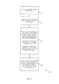
- FIG. 1 is a block diagram of a flash memory decoder system according to various embodiments of the invention.
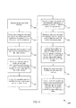
- FIG. 2 is a block diagram of a flash memory decoder according to various embodiments of the invention.
- FIG. 3 is a block diagram of a flash memory decoder system illustrating error detection and correction sub-modules according to various embodiments of the invention.
- FIG. 4 is a block diagram of a flash memory decoder system illustrating an architecture for a decoder controller according to various embodiments of the invention.
- FIG. 5 is a flowchart illustrating a method of decoding data from a flash memory according to various embodiments of the invention.
- FIG. 6 is a flowchart illustrating a method of age responsive decoding of data from a flash memory according to various embodiments of the invention.
- FIG. 7 is a flowchart illustrating a method of decoding data from a flash memory responsive to error rate according to various embodiments of the invention.
- Encoded data from flash memory may be processed to generate a number of data streams.
- a different one of the data streams is processed.
- Each error detection sub-module may detect whether a portion of the respective received stream contains an error, and forward the portion to an error correction module.
- An error correction module physically separate from the error detection sub-modules, may correct the forwarded portions.
- the age and error rate associated with the flash memory may be monitored, and a coding rate or other aspects may be dynamically adapted to account for these factors.
- NAND flash technologies There are two primary NAND flash technologies. The earlier versions of NAND flash were Single-Level Cell (SLC). With SLC Flash, there is only one programmed state in addition to the erased state. The total of two states allows a single data bit to be stored in the memory cell. The desire for higher density led to the more advanced Multiple-Level Cell (MLC). With MLC flash, there are multiple programmed states in addition to the erased state which allows multiple bits to be stored per memory cell.
- SLC Flash Single-Level Cell
- MLC Flash Multiple-Level Cell
- MLC flash there are multiple programmed states in addition to the erased state which allows multiple bits to be stored per memory cell.
- FEC may be one of the tools used to address these bit errors to improve the reliability and lifespan of flash memory.
- FIG. 1 a flash memory system 100 is illustrated.
- the system includes an encoder 105, flash memory 110, a decoder115, and a controller 120.
- This flash memory system 100 may be a stand-alone device, or may be integrated (in whole or in part) with a computer, server, phone or mobile device, tablet, television, or any other computing device.
- the encoder 105, decoder 115, and controller 120 may, individually or collectively, be implemented with one or more Application Specific Integrated Circuits (ASICs) adapted to perform some or all of the applicable functions in hardware.
- ASICs Application Specific Integrated Circuits
- the functions may be performed by one or more other processing units (or cores), on one or more integrated circuits.
- other types of integrated circuits may be used (e.g., Structured/Platform ASICs, Field Programmable Gate Arrays (FPGAs), and other Semi-Custom ICs), which may be programmed in any manner known in the art.
- the functions of each unit may also be implemented, in whole or in part, with instructions embodied in a memory, formatted to be executed by one or more general or application-specific processors.
- the encoder 105 may receive data to be stored, and encode the data (e.g., adding parity information) for storage in the flash memory 110 as encoded data.
- the decoder 115 may include a number of sub-components (not shown).
- An embodiment of the decoder 115 includes an error correction module in communication with and physically separate from an error detection module.
- the decoder 115 may process the encoded data to generate a number of data streams (which may, but need not be, decoded in whole or in part).
- the decoder 115 may process each stream at a different error detection sub-module operating in parallel in the decoder 115.
- Each error detection sub-module may detect whether a portion of the respective received stream contains an error, and then forward the portion of the respective received stream containing an error to the error correction module.
- the error correction module may correct the forwarded portions of the respective received streams containing an error.
- the error detection module may detect and flag bit errors, and this may allow sectors of memory with errors exceeding a threshold amount to be avoided by replacing such sectors with other sectors from a pool of available substitutes.
- the encoder 105 may, also or alternatively, change the code rate for the error-laden sections. As flash become more dense, the inherent bit error probability becomes higher.
- Bose Chaudhuri Hocqunghem (BCH) codes may be used, including the binary BCH and non-binary BCH (Reed Solomon (RS)) codes. These codes offer a higher correction capacity in comparison to the Hamming Code.
- BCH encoding/decoding architectures may be the foundation of error correction in flash memory. However, there are more advanced coding options that may in some instances provide better performance than BCH codes. These codes may be used in flash memory 110, particularly for higher density flash and in applications where performance demands increase. Convolutional Turbo Codes (CTCs), Turbo Product Codes (TPCs), and low density parity check codes (LDPCs) are examples of the coding schemes that may be used. These state-of-the-art codes perform very close to the theoretical limits (Shannon Limits) of error correction, providing very high coding gain and improvement in Bit Error Rate (BER) performance for a given amount of redundancy.
- CTCs Convolutional Turbo Codes
- TPCs Turbo Product Codes
- LDPCs low density parity check codes
- the correction capacity can be expressed as the number of bits a code can correct over a codeword length, or an input BER, or probability of error that it can take down to a certain target decoded BER.
- the advanced codes may correct more errors over a certain length, or take a higher input BER to create the same decoded BER.
- flash memory 110 There is incentive to use advanced codes for flash memory 110 even with not so dense memories. If the inherent error performance of flash memory 110 stayed at a certain low level, there would probably be decreased need for advanced codes. But, in practice, flash memory 110 performance tends to degrade over time. This means that even with an advanced code to help improve the reliability of a flash memory 110, over time the flash memory 110 may become lossy and, once the error rate is high enough, it may be beyond repair by the code being used.
- the rate of errors or age of the flash memory 110 may be monitored, and the coding rate for data to be stored on the flash memory 110 may be modified in response thereto.
- a more robust coding rate may be used as the decoded error rate increases.
- the error monitoring may take place on a per-sector basis, and the code rate modification may similarly take place on a per-sector basis.
- the rate of errors or age of the flash memory 110 may be monitored, and error correction sub-modules may be powered-up in response thereto. Power savings may be achieved by keeping certain error correction sub-modules in an inactive mode until the flash memory reaches a certain age.
- the flash memory 110 may be partitioned into a pool of small fixed-size sectors, and FEC may be applied on a sector-by-sector basis.
- the flash memory 110 size may be defined by the number of sectors that it contains. As there is a chance of sectors going bad over time, there may be a reserve/spare sector pool that allows the controller to replace the bad sectors by the spares as needed to extend the life of the flash.
- the error detection sub-module and error correction sub-modules may be dynamically assigned to various sectors, and the number powered-on may be increased or decreased.
- p good may be a function of use time for the flash memory 110 sector. This is a component that is dependent upon the correction capacity of the code used. Thus, even with the spare sectors and the wear-leveling technique, the codes may play a key role in the flash being usable after a certain use time.
- TPC and LDPC codes offer an excellent degree of freedom in selecting the various code parameters like information block size, coded block size, and correction capacity, and would allow customization to suit any number of flash configurations.
- FIG. 2 is a block diagram 200 of a flash memory decoder 115-a according to various embodiments of the invention.
- the flash memory decoder 115-a may, for example, be the decoder 115 of FIG. 1 , although flash memory decoder 115-a may be implemented in a number of other systems and devices, as well.
- the flash memory decoder 115-a includes a decoder module 205, an error detection module 210, and an error correction module 215, and each of may be in communication with each other.
- the error detection module 210 includes a number of sub-modules configured to detect errors on decoded streams of data.
- the error correction module 215 may be physically separate from each error detection sub-module, and may also include a number of sub-modules (each of which may be time-shared by a number of error detection sub-modules.
- ASICs Application Specific Integrated Circuits
- the functions may be performed by one or more other processing units (or cores), on one or more integrated circuits.
- other types of integrated circuits e.g., Structured/Platform ASICs, Field Programmable Gate Arrays (FPGAs), and other Semi-Custom ICs
- the functions of each unit may also be implemented, in whole or in part, with instructions embodied in a memory, formatted to be executed by one or more general or application-specific processors.
- the decoder module 205 may receive encoded data from flash memory, and process the received encoded data to generate a number of data streams.
- the decoder module processor may buffer, de-interleave, or perform certain aspects of the decoding process, an thereby generate decoded (or partially decoded) data streams.
- the error detection module 210 may include a number of error detection sub-modules operating in parallel. Each (or a subset) of the error detection sub-modules may receive a different one of the data streams, and evaluate the respective stream to determine whether a portion of the stream contains an error.
- Each error detection sub-module may forward the portion of the respective received stream containing an error to the error correction module 215 (bypassing the error correction module 215 with the error-free portions).
- the error correction module 215 corrects the received portions of the respective received streams containing an error.
- the error correction module 215 may include a number of sub-modules (each of which may be time-shared by a number of error detection sub-modules).
- FIG. 3 is a block diagram illustrating an example of an architecture for a flash memory decoder system 300 more particularly illustrating error detection and correction sub-modules.
- the flash memory decoder system 300 may, for example, be the system 100 of FIG. 1 .
- the flash memory decoder system 300 includes flash memory 110-a, a decoder module 205-a, an error detection module 210-a, an error correction module 215-a, a controller 120-a, and an encoder 105-a. Each of these components may be in communication with each other.
- the flash memory 110-a includes a number of different sets of one or more active sectors 305.
- the decoder module 205-a includes a number of decoder sub-modules 310, and each decoder sub-module 310 may be associated with a different set of sectors 305.
- the error detection module 210-a includes a number of error detection sub-modules 315, and each decoder sub-module 310 may be associated with a different set of sectors 305.
- encoded data may be read from a set of one or more of sectors 305 (e.g., sector(s) 305-a) by a decoder sub-module 310 (e.g., decoder sub-module 310-a), and processed (e.g., buffered, de-interleaved, decoded to some extent, etc.) to generate a data stream.
- the data stream may be forwarded to an error detection sub-module 315 (error detection sub-module 315-a).
- encoded data from a set of one or more of sectors 305-a may be sent to an error detection sub-module 315-a.
- Different sets of sectors 305 may each send their respective data via different decoder sub-modules 310, as illustrated.
- each error detection sub-module 315 is distinct from each other.
- the decoder sub-module 310 and error detection sub-module 315 may be integrated to varying degrees.
- Each error detection sub-module 315 may evaluate the respective stream to determine whether a portion of the stream contains an error. Each error detection sub-module 315 may forward the portion of the respective received stream containing an error to the error correction module 215-a (bypassing the error correction module 215 with the error-free portions).
- the error correction module 215-a includes a number of error correction sub-modules 320, each error correction sub-module 320 responsible for handling the errors from a number of error detection sub-modules 315 (e.g., error correction sub-module 320 may correct errors from error detection sub-modules 315-a, -b, and -c). Error correction sub-modules 320 may correct the received portions of the respective received streams containing an error. Each error correction sub-module 320 may receive portions of streams with errors, and these portion may have been detected in parallel.
- Controller 120-a may perform a number of functions in the decoder process. Controller 120-a may dynamically modify the error detection sub-modules 315 and the error correction sub-modules 320 assigned to sectors 305 of flash memory 110-a. The controller 120-a may selectively power-up one or more of the error correction sub-modules 320 responsive to a monitored age or error rate associated with the flash memory 110-a. The controller 120-a may perform this monitoring on a per-sector basis, and the error correction sub-modules 320 may be powered-up to serve the sectors 305 where the error rates exceed a threshold. The controller 120-a may adapt the coding rate to be used by the encoder responsive to a monitored age or error rate associated with the flash memory 110-a. The controller 120-a may perform this monitoring on a per-sector basis, and the controller 120-a may adapt the coding rate on a per sector basis.
- FIG. 4 is a block diagram of a flash memory decoder system 400 illustrating certain controller functionality according to various embodiments of the invention.
- the system 400 includes an encoder 105-b, flash memory 110-b, a decoder115-b, and a controller 120-b.
- This system 400 may be an example of the system 100 of FIG. 1 , and a component of this system 400 may have the same functionality as the counterpart component from FIG. 1
- This flash memory system 400 may be a stand-alone device, or may be integrated (in whole or in part) with a computer, server, phone, mobile device, tablet, television, or any other computing device.
- the controller 120-b includes an adaptive encoding rate controller 405, a power controller 410, a write controller 415, a read controller 420, an age monitoring module 425, and an error monitoring module 430.
- the age monitoring module 425 may monitor an age associated with the flash memory 110-b. This may be a time since manufacture, a time since first use, an amount of use, or any other metric which corresponds to the aging of the flash memory 110-b. This monitoring may involve direct monitoring of the flash memory 110-b itself, or may be based on reports from the encoder 105-b, decoder 115-b, or other components of the system.
- the error monitoring module 430 may monitor an amount of errors associated with the flash memory 110-b. This monitoring may measure errors over a variety of time periods and metrics, and may be translated into an error rate. The monitoring may be performed on a per-sector (or per set of sectors) basis. A number of sampling and averaging techniques may be used. This monitoring may involve direct monitoring of the decoder 115-b itself, or may be based on reports from the decoder 115-b or other components of the system.
- the adaptive encoding rate controller 405 may receive information on the rate and/or amount of errors from the error monitoring module 430.
- the adaptive encoding rate controller 405 may modify a coding rate to be used by the encoder 105-b when the monitored rate and/or amount of errors exceeds a threshold.
- the monitoring of errors may be performed on a per-sector, per set of sectors, or other regional basis.
- the coding rate to be used by the encoder 105-b may be modified when the monitored rate of errors for the applicable region exceeds a threshold.
- the coding rate may be adapted to be more, or less, robust; in other embodiments, the adaptation is only to make the coding rate more robust.
- the adaptive encoding rate controller 405 may receive information on the age of the flash memory 110-b from the age monitoring module 425.
- the adaptive encoding rate controller 405 may adapt the coding rate based on this monitoring (e.g., implementing a more robust coding rate for one or more sectors of the flash memory 110-b when the age exceeds a threshold).
- these threshold may be adaptive to the amount of flash memory 110-b that remains available (e.g., the margin may be increased when the flash memory is utilized below a threshold amount).
- an decoder module 115 may include a number of error correction sub-modules.
- the power controller 410 may receive information on the age of the flash memory 100-b from the age monitoring module 425.
- the power controller 410 may selectively power-up (or power-down) one or more of the error correction sub-modules responsive to an age of the flash memory 110-b.
- the power controller 410 may receive information on the rate and/or amount of errors from the error monitoring module 430.
- the power controller 410 may power-up (or power-down) one or more of the error correction sub-modules (e.g., when the monitored rate and/or amount of errors exceeds a threshold).
- the monitoring of errors may be performed on a per-sector, per set of sectors, or other regional basis.
- the power-up or power-down may be specific to a particular error correction sub-module for a given region of flash memory 110-b.
- the write controller 415 may change the sectors of flash memory 110-b to be written to. These changes may be made in response to information from the age monitoring module 425 and error monitoring module 430.
- the read controller 420 may dynamically change the components of the decoder 115-b to be used to read different sectors of flash memory 110-b (e.g., in FIG. 3 , the assignments of the decoder sub-modules 310, error detection sub-modules 315, and error correction sub-modules 320 may be changed in response to code rate modifications, increased errors, or age).
- FIG. 5 is a flowchart illustrating a method 500 of decoding data from a flash memory according to various embodiments of the invention.
- the method 500 may, for example, be performed in whole or in part by the system 100, 300, or 400 of FIG. 1 , 3 , or 4 or, more specifically, by the decoder 115 of FIG. 1 , 2 , or 4.
- encoded data from a flash memory is received.
- the received encoded data is processed to generate a number of data streams.
- the information for each data stream may be a wholly or partially decoded before being forwarded to respective error correction sub-modules.
- a different one of the data streams is processed.
- Each error detection sub-module is configured to: detect whether a portion of the respective received stream contains an error, and forward the portion of the respective received stream containing an error to an error correction module.
- the error correction module physically separate from the error detection sub-modules, the forwarded portions of the respective received streams containing an error are corrected.
- FIG. 6 is a flowchart illustrating a method of age responsive decoding of data from a flash memory according to various embodiments of the invention.
- the method 600 may, for example, be performed in whole or in part by the system 100, 300, or 400 of FIG. 1 , 3 , or 4.
- the method 600 may be an example of the method 500 of FIG. 5 .
- an age of a flash memory is monitored.
- the coding rate for data to be encoded and stored in the flash memory is modified responsive to a first age threshold of the flash memory.
- data is encoded at the modified rate, and the encoded data is stored on the flash memory.
- one or more error correction sub-modules of an error correction module are powered-up from an inactive mode responsive to a second age threshold of the flash memory.
- the encoded data from the flash memory is processed to generate a number of partially decoded data streams.
- a different one of the data streams is processed.
- a determination is made at each error detection sub-module whether a portion of the respective received stream contains an error.
- error detection sub-modules forward those portions of the respective streams containing an error to the error correction module physically separate from the error detection sub-modules.
- the error-free portions are forwarded to bypass the error correction module.
- the portions of the respective received streams containing an error are corrected with the powered-up error correction modules and additional error correction modules.
- FIG. 7 is a flowchart illustrating a method of decoding data from a flash memory responsive to error rate according to various embodiments of the invention.
- the method 700 may, for example, be performed in whole or in part by the system 100, 300, or 400 of FIG. 1 , 3 , or 4.
- the method 700 may be an example of the method 500 of FIG. 5 or the method 600 of FIG. 6 .
- a rate of errors from an error detection module is monitored for each of a number of sectors of the flash memory.
- the coding rate for data to be encoded and stored in one or more sectors is modified responsive to the monitoring of first error rate threshold for the one or more sectors.
- data is encoded at the modified rate and stored in the one or more sectors.
- an error correction sub-module assigned to the one or more sectors are powered-up from an inactive mode responsive to the monitoring of a second error rate threshold for the one or more sectors.
- the encoded data from the one or more sectors is decoded to generate a decoded data stream.
- the decoded data stream is processed.
- a determination is made by the error detection sub-module that a portion of the respective received stream contains an error.
- the portion of the received stream containing an error is forwarded to the powered-up error correction sub-module.
- the forwarded portion is corrected with the powered-up error correction sub-module.
- the embodiments may be described as a process which is depicted as a flow diagram or block diagram. Although each may describe the operations as a sequential process, many of the operations can be performed in parallel or concurrently. In addition, the order of the operations may be rearranged. A process may have additional steps not included in the figure.
- the term “memory” or “memory unit” may represent one or more devices for storing data, including read-only memory (ROM), random access memory (RAM), magnetic RAM, core memory, magnetic disk storage mediums, optical storage mediums, flash memory devices, or other computer-readable mediums for storing information.
- ROM read-only memory
- RAM random access memory
- magnetic RAM magnetic RAM
- core memory magnetic disk storage mediums
- optical storage mediums flash memory devices
- computer-readable mediums includes, but is not limited to, portable or fixed storage devices, optical storage devices, wireless channels, a sim card, other smart cards, and various other mediums capable of storing, containing, or carrying instructions or data.
- embodiments may be implemented by hardware, software, firmware, middleware, microcode, hardware description languages, or any combination thereof.
- the program code or code segments to perform the necessary tasks may be stored in a computer-readable medium such as a storage medium. Processors may perform the necessary tasks.
Landscapes
- Engineering & Computer Science (AREA)
- Theoretical Computer Science (AREA)
- Quality & Reliability (AREA)
- Physics & Mathematics (AREA)
- General Engineering & Computer Science (AREA)
- General Physics & Mathematics (AREA)
- Techniques For Improving Reliability Of Storages (AREA)
Applications Claiming Priority (1)
| Application Number | Priority Date | Filing Date | Title |
|---|---|---|---|
| US23491109P | 2009-08-18 | 2009-08-18 |
Publications (2)
| Publication Number | Publication Date |
|---|---|
| EP2299362A2 true EP2299362A2 (de) | 2011-03-23 |
| EP2299362A3 EP2299362A3 (de) | 2011-05-04 |
Family
ID=43558319
Family Applications (1)
| Application Number | Title | Priority Date | Filing Date |
|---|---|---|---|
| EP10173328A Withdrawn EP2299362A3 (de) | 2009-08-18 | 2010-08-18 | Vorwärtsfehlerkorrektur für Speicher |
Country Status (2)
| Country | Link |
|---|---|
| US (2) | US8615700B2 (de) |
| EP (1) | EP2299362A3 (de) |
Cited By (4)
| Publication number | Priority date | Publication date | Assignee | Title |
|---|---|---|---|---|
| WO2013138115A1 (en) * | 2012-03-15 | 2013-09-19 | Sandisk Technologies Inc. | Statistical distribution based variable-bit error correction coding |
| US8615700B2 (en) | 2009-08-18 | 2013-12-24 | Viasat, Inc. | Forward error correction with parallel error detection for flash memories |
| WO2017003527A1 (en) * | 2015-07-01 | 2017-01-05 | Xilinx, Inc. | Variable code rate solid-state drive |
| DE112012006153B4 (de) | 2012-03-28 | 2021-09-23 | Intel Corp. | Rekonstruktion von Codewörtern unter Verwendung eines Seitenkanals |
Families Citing this family (21)
| Publication number | Priority date | Publication date | Assignee | Title |
|---|---|---|---|---|
| US9141473B2 (en) * | 2011-03-25 | 2015-09-22 | Samsung Electronics Co., Ltd. | Parallel memory error detection and correction |
| US8856616B1 (en) * | 2011-07-29 | 2014-10-07 | Proton Digital Systems, Inc. | Two dimensional encoding for non-volatile memory blocks |
| US8832506B2 (en) * | 2012-01-20 | 2014-09-09 | International Business Machines Corporation | Bit error rate based wear leveling for solid state drive memory |
| TWI455140B (zh) * | 2012-02-21 | 2014-10-01 | Fluiditech Ip Ltd | Flash memory usage period assessment method |
| US20130262942A1 (en) * | 2012-03-27 | 2013-10-03 | Yung-Chiang Chu | Flash memory lifetime evaluation method |
| US8996961B2 (en) * | 2012-12-11 | 2015-03-31 | Seagate Technology Llc | Error correction code rate management for nonvolatile memory |
| US9094132B1 (en) | 2013-01-23 | 2015-07-28 | Viasat, Inc. | High data rate optical transport network using 8-PSK |
| TWI533316B (zh) * | 2013-03-18 | 2016-05-11 | 慧榮科技股份有限公司 | 錯誤修正方法以及記憶體裝置 |
| SG10201406377VA (en) * | 2013-10-07 | 2015-05-28 | Agency Science Tech & Res | Normalization factor adaptation for ldpc decoding for hard disk drive systems |
| US9477550B2 (en) | 2013-10-24 | 2016-10-25 | Globalfoundries Inc. | ECC bypass using low latency CE correction with retry select signal |
| JP6200381B2 (ja) * | 2014-06-11 | 2017-09-20 | ファナック株式会社 | 監視対象の稼働状況に応じた誤り訂正機能を有する制御装置 |
| US9442787B2 (en) * | 2014-06-13 | 2016-09-13 | Sandisk Technologies Llc | Three dimensional (3D) memory including error detection circuitry |
| US10116336B2 (en) * | 2014-06-13 | 2018-10-30 | Sandisk Technologies Llc | Error correcting code adjustment for a data storage device |
| US9772900B2 (en) * | 2014-07-10 | 2017-09-26 | Samsung Electronics Co., Ltd. | Tiered ECC single-chip and double-chip Chipkill scheme |
| US9606851B2 (en) | 2015-02-02 | 2017-03-28 | International Business Machines Corporation | Error monitoring of a memory device containing embedded error correction |
| US9940457B2 (en) | 2015-02-13 | 2018-04-10 | International Business Machines Corporation | Detecting a cryogenic attack on a memory device with embedded error correction |
| US9983963B2 (en) * | 2015-11-09 | 2018-05-29 | Alibaba Group Holding Limited | System and method for exploiting hard disk drive capacity reserve and extending operating life thereof |
| JP6725375B2 (ja) | 2016-09-14 | 2020-07-15 | キオクシア株式会社 | メモリシステムおよび方法 |
| US10644727B2 (en) * | 2018-01-11 | 2020-05-05 | Western Digital Technologies, Inc. | Code rate switching mechanism for flash memory |
| CN108683426B (zh) * | 2018-05-18 | 2022-08-26 | 中国科学院微电子研究所 | 一种基于bch码的ecc系统及存储器 |
| US11416333B2 (en) * | 2019-08-22 | 2022-08-16 | Micron Technology, Inc. | Semiconductor device with power-saving mode and associated methods and systems |
Family Cites Families (54)
| Publication number | Priority date | Publication date | Assignee | Title |
|---|---|---|---|---|
| US5699365A (en) * | 1996-03-27 | 1997-12-16 | Motorola, Inc. | Apparatus and method for adaptive forward error correction in data communications |
| JP4074029B2 (ja) * | 1999-06-28 | 2008-04-09 | 株式会社東芝 | フラッシュメモリ |
| US7333364B2 (en) * | 2000-01-06 | 2008-02-19 | Super Talent Electronics, Inc. | Cell-downgrading and reference-voltage adjustment for a multi-bit-cell flash memory |
| US20080282128A1 (en) * | 1999-08-04 | 2008-11-13 | Super Talent Electronics, Inc. | Method of Error Correction Code on Solid State Disk to Gain Data Security and Higher Performance |
| US7690031B2 (en) * | 2000-01-06 | 2010-03-30 | Super Talent Electronics, Inc. | Managing bad blocks in flash memory for electronic data flash card |
| US7890846B2 (en) * | 2000-01-06 | 2011-02-15 | Supertalent Electronics, Inc. | Electronic data flash card with Reed Solomon error detection and correction capability |
| US6684353B1 (en) * | 2000-12-07 | 2004-01-27 | Advanced Micro Devices, Inc. | Reliability monitor for a memory array |
| US6961890B2 (en) * | 2001-08-16 | 2005-11-01 | Hewlett-Packard Development Company, L.P. | Dynamic variable-length error correction code |
| JP4437519B2 (ja) * | 2001-08-23 | 2010-03-24 | スパンション エルエルシー | 多値セルメモリ用のメモリコントローラ |
| JP2003250154A (ja) * | 2002-02-22 | 2003-09-05 | Canon Inc | 画像処理装置及びその制御方法 |
| US6751766B2 (en) * | 2002-05-20 | 2004-06-15 | Sandisk Corporation | Increasing the effectiveness of error correction codes and operating multi-level memory systems by using information about the quality of the stored data |
| US20040083334A1 (en) * | 2002-10-28 | 2004-04-29 | Sandisk Corporation | Method and apparatus for managing the integrity of data in non-volatile memory system |
| KR100516586B1 (ko) * | 2002-12-10 | 2005-09-22 | 삼성전자주식회사 | 부호 분할 다중 접속 이동 통신 시스템의 오류 정정 장치및 방법 |
| US7296213B2 (en) * | 2002-12-11 | 2007-11-13 | Nvidia Corporation | Error correction cache for flash memory |
| US7231585B2 (en) * | 2002-12-11 | 2007-06-12 | Nvidia Corporation | Error correction for flash memory |
| US7203874B2 (en) * | 2003-05-08 | 2007-04-10 | Micron Technology, Inc. | Error detection, documentation, and correction in a flash memory device |
| TWI227395B (en) * | 2003-06-02 | 2005-02-01 | Genesys Logic Inc | Method for parallel processing of memory data and error correction code and related device thereof |
| US7356755B2 (en) * | 2003-10-16 | 2008-04-08 | Intel Corporation | Error correction for multi-level cell memory with overwrite capability |
| EP1528702B1 (de) * | 2003-11-03 | 2008-01-23 | Broadcom Corporation | FEC-Dekodierung mit dynamischen Parametern |
| US7210077B2 (en) * | 2004-01-29 | 2007-04-24 | Hewlett-Packard Development Company, L.P. | System and method for configuring a solid-state storage device with error correction coding |
| EP1612950A1 (de) | 2004-06-30 | 2006-01-04 | STMicroelectronics S.r.l. | Verfahren und System zur Korrektur von Fehlern während des Schreiben und Lesens eines nichtflüchtigen Speichers |
| US8402325B2 (en) * | 2004-08-02 | 2013-03-19 | St-Ericsson Sa | Data storage and replay apparatus |
| JP2006048783A (ja) * | 2004-08-02 | 2006-02-16 | Renesas Technology Corp | 不揮発性メモリおよびメモリカード |
| EP1635261B1 (de) * | 2004-09-10 | 2008-06-11 | STMicroelectronics S.r.l. | Speicher mit eingebauter Fehlerkorrekturkode-Einrichtung |
| KR100648281B1 (ko) * | 2005-01-14 | 2006-11-23 | 삼성전자주식회사 | 보안 리던던시 블록을 구비한 낸드 플래시 메모리 장치 |
| US7756050B2 (en) * | 2005-04-29 | 2010-07-13 | Alcatel-Lucent Usa Inc. | Method to provide unequal error protection and unequal error detection for internet protocol applications |
| US7362611B2 (en) * | 2005-08-30 | 2008-04-22 | Micron Technology, Inc. | Non-volatile memory copy back |
| WO2007058617A1 (en) * | 2005-11-17 | 2007-05-24 | Chee Keng Chang | A controller for non-volatile memories, and methods of operating the memory controller |
| US7844879B2 (en) * | 2006-01-20 | 2010-11-30 | Marvell World Trade Ltd. | Method and system for error correction in flash memory |
| JP4577574B2 (ja) * | 2006-02-07 | 2010-11-10 | 日本電気株式会社 | データ送信装置及びデータ受信装置並びにデータ送信方法及びデータ受信方法 |
| US7388781B2 (en) * | 2006-03-06 | 2008-06-17 | Sandisk Il Ltd. | Multi-bit-per-cell flash memory device with non-bijective mapping |
| US7840875B2 (en) * | 2006-05-15 | 2010-11-23 | Sandisk Corporation | Convolutional coding methods for nonvolatile memory |
| US20070266296A1 (en) * | 2006-05-15 | 2007-11-15 | Conley Kevin M | Nonvolatile Memory with Convolutional Coding |
| US7809994B2 (en) * | 2006-05-17 | 2010-10-05 | Sandisk Corporation | Error correction coding for multiple-sector pages in flash memory devices |
| US7304893B1 (en) * | 2006-06-30 | 2007-12-04 | Sandisk Corporation | Method of partial page fail bit detection in flash memory devices |
| KR100833600B1 (ko) * | 2006-08-25 | 2008-05-30 | 삼성전자주식회사 | 에러 정정 회로, 그 방법 및 상기 회로를 구비하는 반도체메모리 장치 |
| US7739576B2 (en) * | 2006-08-31 | 2010-06-15 | Micron Technology, Inc. | Variable strength ECC |
| US20080148132A1 (en) * | 2006-10-26 | 2008-06-19 | Mavila Rajith K | Error detection and correction scheme for multi-level cell NAND flash |
| US8001441B2 (en) * | 2006-11-03 | 2011-08-16 | Sandisk Technologies Inc. | Nonvolatile memory with modulated error correction coding |
| US7706182B2 (en) * | 2006-12-03 | 2010-04-27 | Anobit Technologies Ltd. | Adaptive programming of analog memory cells using statistical characteristics |
| US7877665B2 (en) * | 2006-12-29 | 2011-01-25 | Sandisk Corporation | Page by page ECC variation in a memory device |
| WO2008086237A2 (en) * | 2007-01-05 | 2008-07-17 | California Institute Of Technology | Codes for limited magnitude asymmetric errors in flash memories |
| US7861139B2 (en) * | 2007-01-26 | 2010-12-28 | Micron Technology, Inc. | Programming management data for NAND memories |
| US8055988B2 (en) * | 2007-03-30 | 2011-11-08 | International Business Machines Corporation | Multi-bit memory error detection and correction system and method |
| KR100891332B1 (ko) * | 2007-03-30 | 2009-03-31 | 삼성전자주식회사 | 에러 정정 부호화기를 이용하여 에러를 체크하는 bch에러 정정 방법 및 회로 |
| KR100852193B1 (ko) * | 2007-05-02 | 2008-08-13 | 삼성전자주식회사 | 오류 제어 코드 장치 및 그 방법 |
| US8103942B2 (en) * | 2007-05-24 | 2012-01-24 | Fuji Xerox Co., Ltd. | Data transmission apparatus, data transmission device, data reception device and data transmission system |
| US7930615B2 (en) * | 2007-05-31 | 2011-04-19 | Agere Systems Inc. | Memory device with error correction capability and preemptive partial word write operation |
| US8006166B2 (en) * | 2007-06-12 | 2011-08-23 | Micron Technology, Inc. | Programming error correction code into a solid state memory device with varying bits per cell |
| US8065583B2 (en) * | 2007-07-06 | 2011-11-22 | Micron Technology, Inc. | Data storage with an outer block code and a stream-based inner code |
| CN101527622A (zh) * | 2008-03-07 | 2009-09-09 | 富士通株式会社 | Mimo-harq通信系统和通信方法 |
| US8627169B2 (en) * | 2008-06-20 | 2014-01-07 | Cadence Design Systems, Inc. | Method and apparatus for dynamically configurable multi level error correction |
| US8296620B2 (en) * | 2008-08-26 | 2012-10-23 | Seagate Technology Llc | Data devices including multiple error correction codes and methods of utilizing |
| US8615700B2 (en) | 2009-08-18 | 2013-12-24 | Viasat, Inc. | Forward error correction with parallel error detection for flash memories |
-
2010
- 2010-08-18 US US12/858,510 patent/US8615700B2/en active Active
- 2010-08-18 EP EP10173328A patent/EP2299362A3/de not_active Withdrawn
-
2013
- 2013-11-21 US US14/086,807 patent/US8966347B2/en active Active
Non-Patent Citations (1)
| Title |
|---|
| None |
Cited By (8)
| Publication number | Priority date | Publication date | Assignee | Title |
|---|---|---|---|---|
| US8615700B2 (en) | 2009-08-18 | 2013-12-24 | Viasat, Inc. | Forward error correction with parallel error detection for flash memories |
| US8966347B2 (en) | 2009-08-18 | 2015-02-24 | Viasat, Inc. | Forward error correction with parallel error detection for flash memories |
| WO2013138115A1 (en) * | 2012-03-15 | 2013-09-19 | Sandisk Technologies Inc. | Statistical distribution based variable-bit error correction coding |
| US8862967B2 (en) | 2012-03-15 | 2014-10-14 | Sandisk Technologies Inc. | Statistical distribution based variable-bit error correction coding |
| DE112012006153B4 (de) | 2012-03-28 | 2021-09-23 | Intel Corp. | Rekonstruktion von Codewörtern unter Verwendung eines Seitenkanals |
| WO2017003527A1 (en) * | 2015-07-01 | 2017-01-05 | Xilinx, Inc. | Variable code rate solid-state drive |
| CN107852177A (zh) * | 2015-07-01 | 2018-03-27 | 赛灵思公司 | 可变码率的固态硬盘 |
| CN107852177B (zh) * | 2015-07-01 | 2021-01-01 | 赛灵思公司 | 可变码率的固态硬盘 |
Also Published As
| Publication number | Publication date |
|---|---|
| US8966347B2 (en) | 2015-02-24 |
| US20140157089A1 (en) | 2014-06-05 |
| US8615700B2 (en) | 2013-12-24 |
| US20110047442A1 (en) | 2011-02-24 |
| EP2299362A3 (de) | 2011-05-04 |
Similar Documents
| Publication | Publication Date | Title |
|---|---|---|
| US8966347B2 (en) | Forward error correction with parallel error detection for flash memories | |
| US8656257B1 (en) | Nonvolatile memory controller with concatenated error correction codes | |
| US11714709B2 (en) | Enhanced block management for a memory subsystem | |
| US8281217B2 (en) | Memory devices and encoding and/or decoding methods | |
| US9195539B2 (en) | Method for reading data from block of flash memory and associated memory device | |
| US9176814B2 (en) | Decoding in solid state memory devices | |
| US9319073B2 (en) | Mitigation of write errors in multi-level cell flash memory through adaptive error correction code decoding | |
| US8046660B2 (en) | System and method for correcting errors in non-volatile memory using product codes | |
| JP5345201B2 (ja) | 符号化および/または復号化メモリ装置および方法 | |
| US9317361B2 (en) | Bit-line defect detection using unsatisfied parity code checks | |
| US10498362B2 (en) | Low power error correcting code (ECC) system | |
| US8812939B2 (en) | Soft decoding systems and methods for flash based memory systems | |
| KR101990971B1 (ko) | 메모리, 메모리 시스템, 및 메모리에 대한 에러 검출/정정 방법 | |
| US20120254686A1 (en) | Non-volatile semiconductor memory devices and error correction methods | |
| US20110083060A1 (en) | Memory system and control method for the same | |
| US10896092B2 (en) | Memory components with ordered sweep error recovery | |
| US10447301B2 (en) | Optimal LDPC bit flip decision | |
| US10009045B2 (en) | Decoding method, memory controlling circuit unit and memory storage device | |
| CN101373640A (zh) | 闪存装置以及错误校正方法 | |
| US20170154656A1 (en) | Data programming method and memory storage device | |
| US10942809B2 (en) | Changing of error correction codes based on the wear of a memory sub-system | |
| JP2019057752A (ja) | メモリシステム | |
| US8627183B1 (en) | Systems and methods for storing variable rate product codes | |
| US9170881B2 (en) | Solid state device coding architecture for chipkill and endurance improvement | |
| CN108170554B (zh) | 一种nand的数据编码方法和装置 |
Legal Events
| Date | Code | Title | Description |
|---|---|---|---|
| PUAI | Public reference made under article 153(3) epc to a published international application that has entered the european phase |
Free format text: ORIGINAL CODE: 0009012 |
|
| AK | Designated contracting states |
Kind code of ref document: A2 Designated state(s): AL AT BE BG CH CY CZ DE DK EE ES FI FR GB GR HR HU IE IS IT LI LT LU LV MC MK MT NL NO PL PT RO SE SI SK SM TR |
|
| AX | Request for extension of the european patent |
Extension state: BA ME RS |
|
| PUAL | Search report despatched |
Free format text: ORIGINAL CODE: 0009013 |
|
| AK | Designated contracting states |
Kind code of ref document: A3 Designated state(s): AL AT BE BG CH CY CZ DE DK EE ES FI FR GB GR HR HU IE IS IT LI LT LU LV MC MK MT NL NO PL PT RO SE SI SK SM TR |
|
| AX | Request for extension of the european patent |
Extension state: BA ME RS |
|
| STAA | Information on the status of an ep patent application or granted ep patent |
Free format text: STATUS: THE APPLICATION IS DEEMED TO BE WITHDRAWN |
|
| 18D | Application deemed to be withdrawn |
Effective date: 20111105 |