EP2296203A2 - Organic light-emitting display device - Google Patents
Organic light-emitting display device Download PDFInfo
- Publication number
- EP2296203A2 EP2296203A2 EP10251604A EP10251604A EP2296203A2 EP 2296203 A2 EP2296203 A2 EP 2296203A2 EP 10251604 A EP10251604 A EP 10251604A EP 10251604 A EP10251604 A EP 10251604A EP 2296203 A2 EP2296203 A2 EP 2296203A2
- Authority
- EP
- European Patent Office
- Prior art keywords
- light emitting
- display device
- emitting display
- organic light
- layer
- Prior art date
- Legal status (The legal status is an assumption and is not a legal conclusion. Google has not performed a legal analysis and makes no representation as to the accuracy of the status listed.)
- Withdrawn
Links
Images


Classifications
-
- H—ELECTRICITY
- H10—SEMICONDUCTOR DEVICES; ELECTRIC SOLID-STATE DEVICES NOT OTHERWISE PROVIDED FOR
- H10K—ORGANIC ELECTRIC SOLID-STATE DEVICES
- H10K50/00—Organic light-emitting devices
- H10K50/10—OLEDs or polymer light-emitting diodes [PLED]
- H10K50/11—OLEDs or polymer light-emitting diodes [PLED] characterised by the electroluminescent [EL] layers
- H10K50/125—OLEDs or polymer light-emitting diodes [PLED] characterised by the electroluminescent [EL] layers specially adapted for multicolour light emission, e.g. for emitting white light
-
- H—ELECTRICITY
- H10—SEMICONDUCTOR DEVICES; ELECTRIC SOLID-STATE DEVICES NOT OTHERWISE PROVIDED FOR
- H10K—ORGANIC ELECTRIC SOLID-STATE DEVICES
- H10K50/00—Organic light-emitting devices
- H10K50/80—Constructional details
- H10K50/85—Arrangements for extracting light from the devices
- H10K50/852—Arrangements for extracting light from the devices comprising a resonant cavity structure, e.g. Bragg reflector pair
-
- H—ELECTRICITY
- H10—SEMICONDUCTOR DEVICES; ELECTRIC SOLID-STATE DEVICES NOT OTHERWISE PROVIDED FOR
- H10K—ORGANIC ELECTRIC SOLID-STATE DEVICES
- H10K59/00—Integrated devices, or assemblies of multiple devices, comprising at least one organic light-emitting element covered by group H10K50/00
- H10K59/80—Constructional details
- H10K59/87—Passivation; Containers; Encapsulations
-
- H—ELECTRICITY
- H10—SEMICONDUCTOR DEVICES; ELECTRIC SOLID-STATE DEVICES NOT OTHERWISE PROVIDED FOR
- H10K—ORGANIC ELECTRIC SOLID-STATE DEVICES
- H10K59/00—Integrated devices, or assemblies of multiple devices, comprising at least one organic light-emitting element covered by group H10K50/00
- H10K59/80—Constructional details
- H10K59/875—Arrangements for extracting light from the devices
- H10K59/876—Arrangements for extracting light from the devices comprising a resonant cavity structure, e.g. Bragg reflector pair
-
- H—ELECTRICITY
- H10—SEMICONDUCTOR DEVICES; ELECTRIC SOLID-STATE DEVICES NOT OTHERWISE PROVIDED FOR
- H10K—ORGANIC ELECTRIC SOLID-STATE DEVICES
- H10K2102/00—Constructional details relating to the organic devices covered by this subclass
- H10K2102/301—Details of OLEDs
- H10K2102/351—Thickness
Definitions
- the present invention relates to an organic light emitting display device and, more particularly, to an organic light emitting display device having improved light efficiency.
- Organic light emitting display devices are self-emission type display devices which emit light by applying voltages to an anode, a cathode, and an organic light emitting layer between the anode and the cathode, thereby recombining electrons and holes in the organic light emitting layer.
- white light is emitted from the organic light emitting layer of some display devices, the white light passes through color filters on a light path, thereby realizing color display.
- the white light emitted from the organic light emitting layer passes through the color filters, light efficiency may be deteriorated.
- the present invention sets out to provide an organic light emitting display device having improved light efficiency.
- an organic light emitting display device in an embodiment of the present invention, includes a substrate and a plurality of pixels on the substrate. Each of the pixels is configured to emit light of one of a plurality of second colors for forming white light when combined.
- the plurality of pixels includes a plurality of first electrodes, a second electrode, a white light emitting layer between the first electrodes and the second electrode, and a first thin film layer between the first electrodes and the second electrode.
- the white light emitting layer includes a plurality of light emitting layers, each being configured to emit light of one of a plurality of first colors for forming white light when combined.
- the first thin film layer has a plurality of thicknesses corresponding to the plurality of second colors.
- Each of the plurality of pixels is further configured to emit light of the one of the plurality of second colors when white light emitted from the white light emitting layer causes resonance to occur between the first electrodes and the second electrode.
- the first thin film layer may include at least one selected from the group consisting of a hole injection layer, a hole transport layer, a hole blocking layer, an electron injection layer, an electron transport layer, and an electron blocking layer.
- the first thin film layer may exist in less than all of the plurality of pixels.
- the first thin film layer may be formed by using laser induced thermal imaging (LITI).
- LITI laser induced thermal imaging
- the first thin film layer may be formed by using inkjet printing or nozzle printing.
- the plurality of pixels may further include a second thin film layer between the first electrodes and the second electrode.
- the second thin film layer includes at least one selected from the group consisting of a hole injection layer, a hole transport layer, a hole blocking layer, an electron injection layer, an electron transport layer, and an electron blocking layer.
- the second thin film layer may be concurrently formed for each of the plurality of pixels.
- the plurality of first colors may be the same as the plurality of second colors.
- the plurality of first colors may include three colors.
- the plurality of first colors may include red, green, and blue.
- the plurality of second colors may include three colors.
- the plurality of second colors may include red, green, and blue.
- the organic light emitting display device may further include a pixel-defining layer formed around the first electrodes to define a light emitting region of the plurality of pixels.
- the organic light emitting display device may further include a sealing member on the second electrode to seal the white light emitting layer and the first thin film layer.
- the sealing member may include a substrate formed of glass.
- the sealing member may include a plurality of thin film layers formed by alternating a plurality of organic layers and inorganic layers.
- the organic light emitting display device may further include a filling member between the second electrode and the sealing member.
- the first electrodes and the second electrode may be respectively formed of reflective electrodes and a semitransparent electrode.
- the organic light emitting display device includes a substrate and a plurality of pixels on the substrate. Each of the pixels is configured to emit red, green, or blue light.
- the plurality of pixels includes a plurality of first electrodes, a second electrode, a white light emitting layer between the first electrodes and the second electrode, a first thin film layer between the first electrodes and the second electrode, and color filters.
- the white light emitting layer includes light emitting layers configured to emit red, green, and blue light for forming white light when combined.
- the first thin film layer has a first thickness in each of the plurality of pixels configured to emit red light, a second thickness different than the first thickness in each of the plurality of pixels configured to emit green light, and a third thickness different than the first and second thicknesses in each of the plurality of pixels configured to emit blue light.
- the color filters are in only some of the plurality of pixels based on the color of light emitted by the some of the plurality of pixels.
- Each of the plurality of pixels is further configured to emit the one of red light, green light, or blue light when white light emitted from the white light emitting layer causes resonance to occur between the first electrodes and the second electrode.
- Light in the only some of the plurality of pixels is emitted through the color filters in the only some of the plurality of pixels. Light in remaining ones of the plurality of pixels is emitted without passing through the color filters.
- the first thin film layer may include at least one selected from the group consisting of a hole injection layer, a hole transport layer, a hole blocking layer, an electron injection layer, an electron transport layer, and an electron blocking layer.
- the plurality of pixels may further include a second thin film layer between the first electrodes and the second electrode.
- the second thin film layer may include at least one selected from the group consisting of a hole injection layer, a hole transport layer, a hole blocking layer, an electron injection layer, an electron transport layer, and an electron blocking layer.
- the organic light emitting display device may further include a sealing member on the second electrode to seal the white light emitting layer and the first thin film layer.
- the organic light emitting display device may further include a filling member between the second electrode and the sealing member.
- the first electrodes and the second electrode may be respectively formed of reflective electrodes and a semitransparent electrode.
- the color filters may be on a surface of a sealing member or the substrate.
- the organic light emitting display device may further include black matrix between the color filters.
- FIG. 1 is a cross-sectional view schematically illustrating some pixels in an organic light emitting display device, according to an embodiment of the present invention
- FIG. 2 is a cross-sectional view schematically illustrating some pixels in an organic light emitting display device, according to another embodiment of the present invention.
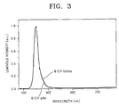
- FIG. 3 is a graph illustrating luminous intensity of blue light before and after passing through a blue color filter in the organic light emitting display device of FIG. 2 .
- the organic light emitting display device 1 includes a plurality of pixels P1, P2, and P3 on a substrate 10.
- the substrate 10 may be formed of a transparent glass material such as SiO 2 .
- the substrate 10 may be also formed of a non-transparent material or may be formed of other materials such as plastic.
- a buffer layer (not illustrated) formed of SiO 2 and/or SiNx may be formed on the substrate 10 in order, for example, for the substrate 10 to provide a flat surface on the substrate and to prevent impurities from penetrating.
- a plurality of thin film transistors (not illustrated) respectively connected to the plurality of pixels P1, P2, and P3 may be formed on the substrate 10.
- Each of the plurality of pixels P1, P2, and P3 may emit a different color (for instance, one of primary colors, such as red, green, or blue). If these colors are optically mixed (or combined), white light may be realized. For convenience of description, it is assumed that the first pixel P1 emits red light, the second pixel P2 emits green light, and the third pixel P3 emits blue light.
- a plurality of first electrodes 21, 22, and 23 and a second electrode 60 are formed (or located) on the substrate 10.
- a white light emitting layer 40, first thin film layers 31 and 32, a second thin film layer 50, a filling member 70, and the second electrode 60 are interposed (or located) between the plurality of first electrodes 21, 22, and 23 and a sealing substrate 80.
- the first electrodes 21, 22, and 23 may be formed in a pattern (for example, a predetermined pattern) by using photolithography.
- a pattern for example, a predetermined pattern
- thicknesses of the first electrodes 21, 22, and 23 respectively formed in the pixels P1, P2, and P3 are the same.
- the organic light emitting display device 1 is a passive matrix (PM) type
- the patterns of the first electrodes 21, 22, and 23 may be stripe-lines that are spaced apart from each other.
- the organic light emitting display device 1 is an active matrix (AM) type
- the first electrodes 21, 22, and 23 may respectively correspond to the pixels P1, P2, and P3.
- the second electrode 60 is disposed (or located) on the first electrodes 21, 22, and 23. If the organic light emitting display device is a PM type, the second electrode 60 may have a stripe form that is perpendicular to the patterns of the first electrodes 21, 22, and 23. On the other hand, if the organic light emitting display device is an AM type, the second electrode 60 may be formed as a common layer throughout an entire active region on which an image is realized.
- the first electrodes 21, 22, and 23 may act as anode electrodes and the second electrode 60 may act as a cathode electrode, or vice versa.
- the first electrodes 21, 22, and 23 and the second electrode 60 that face each other with the white light emitting layer 40 interposed therebetween are formed of a combination of a reflective electrode and a semitransparent electrode.
- the organic light emitting display device 1 is a bottom emission type, whereby an image is realized in a direction of the substrate 10
- the first electrodes 21, 22, and 23 may be semitransparent electrodes and the second electrode 60 may be a reflective electrode.
- the organic light emitting display device 1 is a top emission type, whereby an image is realized in a direction of the sealing substrate 80
- the first electrodes 21, 22, and 23 may be reflective electrodes and the second electrode 60 may be a semitransparent electrode.
- the organic light emitting display device 1 in FIG. 1 is a top emission type, so that the first electrodes 21, 22, and 23 are formed as reflective electrodes and the second electrode 60 is formed as a semitransparent electrode.
- the first electrodes 21, 22, and 23 may be formed of a reflective metal such as silver (Ag), aluminum (AI), gold (Au), platinum (Pt), or chromium (Cr), or an alloy containing one or more of these or other suitable metals.
- the first electrodes 21, 22, and 23 may be formed as a double-layer or a triple-layer further including an indium tin oxide (ITO) layer or an indium zinc oxide (IZO) layer on an upper portion and/or a lower portion of the reflective metal.
- ITO indium tin oxide
- IZO indium zinc oxide
- the second electrode 60 is formed as a common electrode.
- the second electrode 60 may be formed of a semi-reflective/semitransparent metal.
- the semi-reflective/semitransparent metal may be an alloy of magnesium (Mg) and silver (Ag), a metal such as silver (Ag), aluminum (Al), gold (Au), platinum (Pt), or chromium (Cr), or an alloy containing one or more or these or other suitable metals.
- the second electrode 60 may have a sufficient thickness to reach a reflectivity of 5% or more and a transmissivity of 50% or more.
- a pixel-defining layer may be formed outside of (for example, around) the first electrodes 21, 22, and 23 to define a light emitting region.
- First thin film layers 31 and 32 are formed in the pixels P1 and P2 on the first electrodes 21 and 22.
- a thickness t1 of the first thin film layer 31 formed in the first pixel P1 which emits red light
- a thickness t2 of the first thin film layer 32 formed in the second pixel P2 which emits green light
- no first thin film layer is formed in the third pixel P3, which emits blue light.
- the first thin film layers 31 and 32 may include at least one selected from the group consisting of a hole injection layer (HIL), a hole transport layer (HTL), a hole blocking layer (HBL), an electron injection layer (EIL), an electron transport layer (ETL), and an electron blocking layer (EBL).
- HIL hole injection layer
- HTL hole transport layer
- HBL hole blocking layer
- EIL electron injection layer
- ETL electron transport layer
- EBL electron blocking layer
- EBL electron blocking layer
- the first thin film layers 31 and 32 may be formed to each have a different thickness on each pixel by using laser induced thermal imaging (LITI).
- LITI laser induced thermal imaging
- the first thin film layers 31 and 32 may be patterned on each pixel with each different thickness by using inkjet printing or nozzle printing.
- the second thin film layer 50 formed in the plurality of pixels P1, P2, and P3 as a common layer having a same thickness throughout is interposed between the first electrodes 21, 22, and 23 and the second electrode 60.
- the white light emitting layer 40 is interposed between layers of the second thin film layer 50.
- the second thin film layer 50 may include at least one selected from the group consisting of a hole injection layer (HIL), a hole transport layer (HTL), a hole blocking layer (HBL), an electron injection layer (EIL), an electron transport layer (ETL), and an electron blocking layer (EBL).
- HIL hole injection layer
- HTL hole transport layer
- HBL hole blocking layer
- EIL electron injection layer
- ETL electron transport layer
- EBL electron blocking layer
- the second thin film layer 50 sequentially includes a HIL 51, a HTL 52, an ETL 53, and an EIL 54 in a direction from the first electrodes 21, 22, and 23 to the second electrode 60.
- the second thin film layer 50 is not limited to the above selected layers.
- the HIL 51 is formed in each of the pixels P1, P2, and P3 as a common layer.
- the HIL 51 may be formed of a generally used material selected from the group including copper phthalocyanine (CuPc), 4,4',4"-tris(N-(3-methylphenyl)-N-phenylamino)triphenylamine)(MTDATA), and mixtures thereof.
- a HIL is selected as the first thin film layers 31 and 32
- the HIL 51 is selected as one of the layers for forming the second thin film layer 50 as a common layer having the same thickness throughout and is formed on the first thin film layers 31 and 32 in the entire pixels P1 and P2, respectively, and on first electrode 23 in the entire pixel P3. Accordingly, total thicknesses T1, T2, and T3 obtained by adding the first thin film layers 31 and 32 and the HIL 51 of the second thin film layer 50 vary in each pixel P1, P2, and P3.
- the thickness T1 of the HILs 31 and 51 in the first pixel P1 is the largest
- the thickness of the HILs 32 and 51 in the second pixel P2 is less than T1
- the thickness T3 of the HIL 51 in the third pixel P3 is the smallest.
- the HTL 52 is formed on the HIL 51 in the pixels P1, P2, and P3 as a common layer having the same thickness throughout.
- the HTL 52 may be, for example, formed of N,N'-Di(naphthalene-1-yl)-N,N'-diphenyl-benzidine (NPB) or polyethylenedioxythiophene (PEDOT).
- the white light emitting layer 40 sequentially including light emitting layers 41, 42, and 43 that respectively emit red, green, and blue light that are combined to produce white light, is formed on the HTL 52 in the pixels P1, P2, and P3 as a common layer.
- red, green, and blue are selected as a combination for light emitting layers to emit white light.
- the present invention is not limited thereto and various colors, which may combine with each other to emit white light, may be used.
- the order of the layers being stacked does not affect the emitting of white light.
- three emitting layers are separately formed in FIG. 1 .
- two or more luminescent substances may be mixed (or combined) and one layer or two layers may be formed.
- the light emitting layer 41 realizing red light may be formed of a phosphorescent substance which includes carbazole biphenyl (CBP) or mCP as a host material and includes at least one selected from the group including bis(1-phenylisoquinoline)acetylacetonate iridium (PlQlr(acac)), bis(1-phenylquinoline)acetylacetonate iridium PQlr(acac)), tris(1-phenylquinoline) iridium (PQlr), and octaethylporphyrin platinum (PtPEP) as a dopant material.
- the light emitting layer 41 may be formed of a fluorescent substance such as PED:Eu(DBM)3(Phen) or Perylene.
- the light emitting layer 42 realizing green light may be formed of a phosphorescent substance that includes CBP or mCP as a host material and includes fac tris(2-phenylpyridine) iridium (Ir(ppy)3) as a dopant material.
- the light emitting layer 42 may be formed of a fluorescent substance such as tris(8-hydroxyquinoline) aluminum (Alq3).
- the light emitting layer 43 realizing blue light may be formed of a fluorescent substance including one selected from the group consisting of DPVBi, spiro-DPVBi, spiro-6P, distill benzene (DSB), distyrylarylene (DSA), a PFO-based polymer, a PPV-based polymer, and mixtures thereof.
- a fluorescent substance including one selected from the group consisting of DPVBi, spiro-DPVBi, spiro-6P, distill benzene (DSB), distyrylarylene (DSA), a PFO-based polymer, a PPV-based polymer, and mixtures thereof.
- the light emitting layers 41, 42, and 43 respectively emit red, green, and blue light may be formed as a common layer by depositing them in the plurality of pixels P1, P2, and P3 by using one open mask.
- the light emitting layers having each different color may be patterned in each pixel by using laser induced thermal imaging (LITI), inkjet printing, or vacuum depositing using a fine metal mask (FMM). Accordingly, the white light emitting layer 40 according to the embodiment of FIG. 1 may be easily formed without a separate patterning process for each pixel.
- LITI laser induced thermal imaging
- FMM fine metal mask
- HBL hole blocking layer
- the HBL may be formed of biphenoxy-bi(8-quinolitolato)aluminum (Balq).
- the ETL 53 is formed on the white light emitting layer 40 in each pixel P1, P2, and P3 as a common layer with the same thickness.
- the ETL 53 may be formed of a polycyclic hydrocarbon based derivative, a heterocyclic compound, or tris(8-hydroxyquinolinato)aluminum (Alq3).
- the EIL 54 is formed on the ETL in each pixel P1, P2, and P3 as a common layer having the same thickness throughout.
- the EIL 54 may be formed of LiF, Liq, NaF, or Naq.
- FIG. 1 a plurality of thin film layers including the HIL 51, the HTL 52, the ETL 53, and the EIL 54 is illustrated as the second thin film layer 50.
- the present invention is not limited thereto and other thin film layers may be added or removed, if necessary.
- a filling member 70 which is filled with a filler so as to protect the organic light emitting display device 1, may be interposed between the second electrode 60 and the sealing substrate 80.
- the sealing substrate 80 for sealing the first thin film layers 31 and 32, the white light emitting layer 40, and the second thin film layer 50 is formed on the filling member 70.
- the sealing substrate 80 sealed with a sealant (not illustrated) is disposed on the substrate 10; however, the present invention is not limited thereto.
- a sealing structure (not illustrated) of a thin film formed by alternating a plurality of organic layers and inorganic layers may be formed on the filling member 70.
- a typical organic light emitting display device including a white light emitting layer includes color filters (to realize a color display device). Accordingly, white light emitted from the white light emitting layer passes red, green, and blue color filters located in each pixel and emits red light, green light, and blue light in each pixel. Accordingly, different colors are realized in the display device due to combinations of the emitted colors of light.
- red light R is emitted from the first pixel P1
- green light G is emitted from the second pixel P2
- blue light B is emitted from the third pixel P3 without a separate color filter being installed.
- a principle of emitting specific colors in each pixel without color filters is as follows.
- the first electrodes 21, 22, and 23 provide holes and the second electrode 60 provides electrons.
- the holes and electrons are combined in the red light emitting layer 41, the green light emitting layer 42, and the blue light emitting layer 43, excitons (which are particles in an excited state) are generated and the excitons fall to a ground state, thereby emitting, for example, red, green, and blue light.
- the emitted colors of light are optically mixed with each other and the white light emitting layer 40 emits white light.
- the white light emitted from the white light emitting layer 40 causes resonance to occur between the first electrodes 21, 22, and 23, which are reflective electrodes, and the second electrode 60, which is a semi-reflective/semitransparent electrode.
- the thicknesses of the first electrodes 21, 22, and 23, the second electrode 60, the white light emitting layer 40, and the second thin film layer 50 are the same in all pixels P1, and P2, and P3.
- the thicknesses of the first thin film layers 31 and 32 vary according to each pixel P1, P2, and P3.
- the thickness T1 of the HILs 31 and 51 in the first pixel P1 is the largest
- the thickness T2 of the HILs 32 and 51 in the second pixel P2 is less than the thickness T1
- the thickness T3 of the HIL 51 in the third pixel P3 is the smallest. Accordingly, the optical distance of the first pixel is longer than the optical distance of the second pixel P2 and the optical distance of the second pixel P2 is longer than the optical distance of the third pixel P3.
- each respective pixel P1, P2, and P3 strengthens light emission of light that has a wavelength that is close to a wavelength corresponding to a resonant wavelength designed for that pixel P1, P2, and P3, and suppresses light emission of light that has a wavelength that is close to other wavelengths. Accordingly, in the light emitted from the first pixel P1, the second pixel P2, and the third pixel P3, red light R, green light G, and blue light B are respectively strengthened and emitted.
- the first pixel P1 realizes red light
- the second pixel P2 realizes green light
- the third pixel P3 realizes blue light
- each of the pixels P1, P2, and P3 may be configured realize any one of red, green, and blue light regardless of the order.
- a combination of other colors, instead of red, green, and blue, which realize full color may be used.
- full color may be realized by a combination of four or more colors of pixels, instead of three colors of pixels.
- the organic light emitting display device 1 In the organic light emitting display device 1 according to the embodiment of FIG. 1 , color filters are not included. Therefore, problems such as a decrease in light emitting efficiency that takes place when light penetrates a color filter, and high voltage and high current required when color filters are used, may be solved and thus power consumption may be reduced.
- the light emitting layer is not formed by each pixel individually but is instead formed as a common layer, which simplifies fabrication of the light emitting layer.
- FIG. 2 is a cross-sectional view schematically illustrating some pixels in the organic light emitting display device 2
- FIG. 3 is a graph illustrating luminous intensity of blue light before and after the blue light passes through a blue color filter in the organic light emitting display device of FIG. 2 .
- structures in FIG. 2 representing the same or substantially similar structures with those of FIG. 1 use the same reference numerals.
- the organic light emitting display device 2 includes the plurality of first electrodes 21, 22, and 23 on the substrate 10, and the second electrode 60.
- the white light emitting layer 40, the first thin film layers 31 and 32, the second thin film layer 50, the filling member 70, and the second electrode 60 may be interposed between the plurality of first electrodes 21, 22, and 23 and the sealing substrate 80.
- Color filters 90 are located in some of the pixels P1 and P2 among the plurality of pixels P1, P2, and P3 on a surface of the sealing substrate 80 and black matrix BM is alternately arranged between the color filters 90.
- like reference numerals in the organic light emitting display device 2 denote like elements in the organic light emitting display device 1.
- the organic light emitting display device 2 includes the white light emitting layer 40, which emits white light, between the first electrodes 21, 22, and 23, which are reflective electrodes, and the second electrode 60, which is a semitransparent electrode.
- a HIL is selected as the first thin film layers 31 and 32
- the HIL 51 is selected as one of the layers for forming the second thin film layer 50 as a common layer having the same thickness throughout and is formed on the first thin film layers 31 and 32 in all of the pixels P1, P2, and P3. Accordingly, as in the previous embodiment, total thicknesses T1, T2, and T3 obtained by adding the first thin film layers 31 and 32 and the HIL 51 of the second thin film layer 50 vary in each of the pixels P1, P2, and P3.
- the color filters 90 are formed on the surface of the sealing substrate 80.
- the color filters 90 are not located in all colors of pixels as in a typical color filter arrangement, but are instead only located in some colors of pixels.
- a red color filter 90R which allows red light to penetrate
- a green color filter 90G which allows green light to penetrate
- a blue color filter is not located to correspond to the third pixel P3.
- the organic light emitting display device 2 in which optical distances are designed to each have a different length in each pixel P1, P2, and P3 and a fine resonance effect is used, light emission of light that has a wavelength that is close to a wavelength corresponding to the resonant wavelength designed by each pixel P1, P2, and P3 of the white light emitted from the white light emitting layer 40 is strengthened while light emission of light that has a wavelength that is close to other wavelengths is suppressed. Accordingly, in the light emitted from the first pixel P1, the second pixel P2, and the third pixel P3, red light, green light, and blue light are respectively strengthened (e.g., enhanced to improve color purity) and emitted.
- the color gamut may be significantly improved.
- color filters for all of the pixels for example, red, green, and blue color filters, are employed, luminous efficiency of the organic light emitting display device is reduced by 1/3.
- the color filters are located in some pixels so that a decrease in luminous efficiency is reduced or minimized while the improved or maximum color gamut is maintained.
- the red light emitted from the first pixel P1 passes through the red color filter 90R so as to be emitted as red light R' having a narrow bandwidth
- the green light emitted from the first pixel P2 passes through the color filter 90G so as to be emitted as green light G' having a narrow bandwidth
- blue light B emitted from the third pixel P3 is directly emitted without passing through the color filter.
- FIG. 3 illustrates an emission spectrum of blue light before and after passing through a blue color filter in the organic light emitting display device 2 of FIG. 2 .
- emission spectrum characteristics such as bandwidths before and after passing through the color filter are not significantly changed.
- Table 1 below shows changes in characteristics of the organic light emitting display device before and after the blue color filter is employed.
- a blue color filter is not employed so that power consumption of the organic light emitting display device may be reduced due to the decrease in the driving voltage and current for blue light emission (as illustrated in Table 1), which corresponds to a desired brightness. Also, an efficiency decrease caused when the blue color filter is employed does not occur and thus panel efficiency of the organic light emitting display device may increase. In addition, some color filters (red and green) are employed and thus the color gamut of the organic light emitting display device may be strengthened. Moreover, the light emitting layer is not formed separately by each individual pixel but instead is formed as a common layer, and thus the light emitting layer fabrication may be simplified.
- the organic light emitting display device in which the blue color filter is not employed is described.
- the present invention is not limited thereto. That is, red and/or green color filters may not be employed if power consumption is reduced and efficiency decrease does not occur while the same emission characteristics (color coordinates and emission spectrum) are substantially maintained.
- the organic light emitting display device of embodiments of the present invention all or some of the color filters are not employed so that problems such as a decrease in efficiency caused by light penetrating the color filters, and high voltage and high current required when the color filters are used, may be solved, and thus power consumption may be reduced.
- the light emitting layer is not formed by each pixel but is instead formed as a common layer so that the light emitting layer may be fabricated more simply.
Landscapes
- Physics & Mathematics (AREA)
- Optics & Photonics (AREA)
- Electroluminescent Light Sources (AREA)
- Devices For Indicating Variable Information By Combining Individual Elements (AREA)
Abstract
Description
- The present invention relates to an organic light emitting display device and, more particularly, to an organic light emitting display device having improved light efficiency.
- Organic light emitting display devices are self-emission type display devices which emit light by applying voltages to an anode, a cathode, and an organic light emitting layer between the anode and the cathode, thereby recombining electrons and holes in the organic light emitting layer. When white light is emitted from the organic light emitting layer of some display devices, the white light passes through color filters on a light path, thereby realizing color display. However, when the white light emitted from the organic light emitting layer passes through the color filters, light efficiency may be deteriorated.
- The present invention sets out to provide an organic light emitting display device having improved light efficiency.
- In an embodiment of the present invention, an organic light emitting display device is provided. The organic light emitting display device includes a substrate and a plurality of pixels on the substrate. Each of the pixels is configured to emit light of one of a plurality of second colors for forming white light when combined. The plurality of pixels includes a plurality of first electrodes, a second electrode, a white light emitting layer between the first electrodes and the second electrode, and a first thin film layer between the first electrodes and the second electrode. The white light emitting layer includes a plurality of light emitting layers, each being configured to emit light of one of a plurality of first colors for forming white light when combined. The first thin film layer has a plurality of thicknesses corresponding to the plurality of second colors. Each of the plurality of pixels is further configured to emit light of the one of the plurality of second colors when white light emitted from the white light emitting layer causes resonance to occur between the first electrodes and the second electrode.
- The first thin film layer may include at least one selected from the group consisting of a hole injection layer, a hole transport layer, a hole blocking layer, an electron injection layer, an electron transport layer, and an electron blocking layer.
- The first thin film layer may exist in less than all of the plurality of pixels.
- The first thin film layer may be formed by using laser induced thermal imaging (LITI).
- The first thin film layer may be formed by using inkjet printing or nozzle printing.
- The plurality of pixels may further include a second thin film layer between the first electrodes and the second electrode.
- The second thin film layer includes at least one selected from the group consisting of a hole injection layer, a hole transport layer, a hole blocking layer, an electron injection layer, an electron transport layer, and an electron blocking layer.
- The second thin film layer may be concurrently formed for each of the plurality of pixels.
- The plurality of first colors may be the same as the plurality of second colors.
- The plurality of first colors may include three colors.
- The plurality of first colors may include red, green, and blue.
- The plurality of second colors may include three colors.
- The plurality of second colors may include red, green, and blue.
- The organic light emitting display device may further include a pixel-defining layer formed around the first electrodes to define a light emitting region of the plurality of pixels.
- The organic light emitting display device may further include a sealing member on the second electrode to seal the white light emitting layer and the first thin film layer.
- The sealing member may include a substrate formed of glass.
- The sealing member may include a plurality of thin film layers formed by alternating a plurality of organic layers and inorganic layers.
- The organic light emitting display device may further include a filling member between the second electrode and the sealing member.
- The first electrodes and the second electrode may be respectively formed of reflective electrodes and a semitransparent electrode.
- According to another embodiment of the present invention, another organic light emitting display device is provided. The organic light emitting display device includes a substrate and a plurality of pixels on the substrate. Each of the pixels is configured to emit red, green, or blue light. The plurality of pixels includes a plurality of first electrodes, a second electrode, a white light emitting layer between the first electrodes and the second electrode, a first thin film layer between the first electrodes and the second electrode, and color filters. The white light emitting layer includes light emitting layers configured to emit red, green, and blue light for forming white light when combined. The first thin film layer has a first thickness in each of the plurality of pixels configured to emit red light, a second thickness different than the first thickness in each of the plurality of pixels configured to emit green light, and a third thickness different than the first and second thicknesses in each of the plurality of pixels configured to emit blue light. The color filters are in only some of the plurality of pixels based on the color of light emitted by the some of the plurality of pixels. Each of the plurality of pixels is further configured to emit the one of red light, green light, or blue light when white light emitted from the white light emitting layer causes resonance to occur between the first electrodes and the second electrode. Light in the only some of the plurality of pixels is emitted through the color filters in the only some of the plurality of pixels. Light in remaining ones of the plurality of pixels is emitted without passing through the color filters.
- The first thin film layer may include at least one selected from the group consisting of a hole injection layer, a hole transport layer, a hole blocking layer, an electron injection layer, an electron transport layer, and an electron blocking layer.
- The plurality of pixels may further include a second thin film layer between the first electrodes and the second electrode.
- The second thin film layer may include at least one selected from the group consisting of a hole injection layer, a hole transport layer, a hole blocking layer, an electron injection layer, an electron transport layer, and an electron blocking layer.
- The organic light emitting display device may further include a sealing member on the second electrode to seal the white light emitting layer and the first thin film layer.
- The organic light emitting display device may further include a filling member between the second electrode and the sealing member.
- The first electrodes and the second electrode may be respectively formed of reflective electrodes and a semitransparent electrode.
- The color filters may be on a surface of a sealing member or the substrate.
- The organic light emitting display device may further include black matrix between the color filters.
- The above and other features of the invention are set out in the appended claims.
- Embodiments of the present invention will be described with reference to the attached drawings in which:
-
FIG. 1 is a cross-sectional view schematically illustrating some pixels in an organic light emitting display device, according to an embodiment of the present invention; -
FIG. 2 is a cross-sectional view schematically illustrating some pixels in an organic light emitting display device, according to another embodiment of the present invention; and -
FIG. 3 is a graph illustrating luminous intensity of blue light before and after passing through a blue color filter in the organic light emitting display device ofFIG. 2 . - Referring to
FIG. 1 , the organic lightemitting display device 1 includes a plurality of pixels P1, P2, and P3 on asubstrate 10. Thesubstrate 10 may be formed of a transparent glass material such as SiO2. Thesubstrate 10 may be also formed of a non-transparent material or may be formed of other materials such as plastic. - In addition, a buffer layer (not illustrated) formed of SiO2 and/or SiNx may be formed on the
substrate 10 in order, for example, for thesubstrate 10 to provide a flat surface on the substrate and to prevent impurities from penetrating. Moreover, in an active matrix organic light emitting display device, a plurality of thin film transistors (not illustrated) respectively connected to the plurality of pixels P1, P2, and P3 may be formed on thesubstrate 10. - Each of the plurality of pixels P1, P2, and P3 may emit a different color (for instance, one of primary colors, such as red, green, or blue). If these colors are optically mixed (or combined), white light may be realized. For convenience of description, it is assumed that the first pixel P1 emits red light, the second pixel P2 emits green light, and the third pixel P3 emits blue light.
- A plurality of
first electrodes second electrode 60 are formed (or located) on thesubstrate 10. A whitelight emitting layer 40, first thin film layers 31 and 32, a secondthin film layer 50, a fillingmember 70, and thesecond electrode 60 are interposed (or located) between the plurality offirst electrodes substrate 80. - The
first electrodes FIG. 1 , thicknesses of thefirst electrodes - If the organic light emitting
display device 1 is a passive matrix (PM) type, the patterns of thefirst electrodes display device 1 is an active matrix (AM) type, thefirst electrodes - The
second electrode 60 is disposed (or located) on thefirst electrodes second electrode 60 may have a stripe form that is perpendicular to the patterns of thefirst electrodes second electrode 60 may be formed as a common layer throughout an entire active region on which an image is realized. Thefirst electrodes second electrode 60 may act as a cathode electrode, or vice versa. - In order to realize a microcavity effect, the
first electrodes second electrode 60 that face each other with the whitelight emitting layer 40 interposed therebetween are formed of a combination of a reflective electrode and a semitransparent electrode. For example, if the organic light emittingdisplay device 1 is a bottom emission type, whereby an image is realized in a direction of thesubstrate 10, thefirst electrodes second electrode 60 may be a reflective electrode. By way of further example, if the organic light emittingdisplay device 1 is a top emission type, whereby an image is realized in a direction of the sealingsubstrate 80, thefirst electrodes second electrode 60 may be a semitransparent electrode. - For ease of description, assume that the organic light emitting
display device 1 inFIG. 1 is a top emission type, so that thefirst electrodes second electrode 60 is formed as a semitransparent electrode. Thefirst electrodes first electrodes - Further, the
second electrode 60 is formed as a common electrode. Thesecond electrode 60 may be formed of a semi-reflective/semitransparent metal. The semi-reflective/semitransparent metal may be an alloy of magnesium (Mg) and silver (Ag), a metal such as silver (Ag), aluminum (Al), gold (Au), platinum (Pt), or chromium (Cr), or an alloy containing one or more or these or other suitable metals. Here, thesecond electrode 60 may have a sufficient thickness to reach a reflectivity of 5% or more and a transmissivity of 50% or more. - Although not illustrated in
FIG. 1 , a pixel-defining layer (PDL) may be formed outside of (for example, around) thefirst electrodes - First thin film layers 31 and 32, each having a different thickness, are formed in the pixels P1 and P2 on the
first electrodes FIG. 1 , a thickness t1 of the firstthin film layer 31 formed in the first pixel P1, which emits red light, is the largest, while a thickness t2 of the firstthin film layer 32 formed in the second pixel P2, which emits green light, is less than the thickness t1 of the firstthin film layer 31 formed in the first pixel P1. In the embodiment shown inFIG. 1 , no first thin film layer is formed in the third pixel P3, which emits blue light. - The first thin film layers 31 and 32 may include at least one selected from the group consisting of a hole injection layer (HIL), a hole transport layer (HTL), a hole blocking layer (HBL), an electron injection layer (EIL), an electron transport layer (ETL), and an electron blocking layer (EBL). For example, in
FIG. 1 , the hole injection layer (HIL) is selected as the first thin film layers 31 and 32. - The first thin film layers 31 and 32 may be formed to each have a different thickness on each pixel by using laser induced thermal imaging (LITI). In addition, the first thin film layers 31 and 32 may be patterned on each pixel with each different thickness by using inkjet printing or nozzle printing.
- The second
thin film layer 50 formed in the plurality of pixels P1, P2, and P3 as a common layer having a same thickness throughout is interposed between thefirst electrodes second electrode 60. In addition, the whitelight emitting layer 40 is interposed between layers of the secondthin film layer 50. The secondthin film layer 50 may include at least one selected from the group consisting of a hole injection layer (HIL), a hole transport layer (HTL), a hole blocking layer (HBL), an electron injection layer (EIL), an electron transport layer (ETL), and an electron blocking layer (EBL). - For example, in
FIG. 1 , the secondthin film layer 50 sequentially includes aHIL 51, aHTL 52, anETL 53, and anEIL 54 in a direction from thefirst electrodes second electrode 60. However, the secondthin film layer 50 is not limited to the above selected layers. - The
HIL 51 is formed in each of the pixels P1, P2, and P3 as a common layer. TheHIL 51 may be formed of a generally used material selected from the group including copper phthalocyanine (CuPc), 4,4',4"-tris(N-(3-methylphenyl)-N-phenylamino)triphenylamine)(MTDATA), and mixtures thereof. - For example, in
FIG. 1 , a HIL is selected as the first thin film layers 31 and 32, and theHIL 51 is selected as one of the layers for forming the secondthin film layer 50 as a common layer having the same thickness throughout and is formed on the first thin film layers 31 and 32 in the entire pixels P1 and P2, respectively, and onfirst electrode 23 in the entire pixel P3. Accordingly, total thicknesses T1, T2, and T3 obtained by adding the first thin film layers 31 and 32 and theHIL 51 of the secondthin film layer 50 vary in each pixel P1, P2, and P3. That is, the thickness T1 of theHILs HILs HIL 51 in the third pixel P3 is the smallest. - The
HTL 52 is formed on theHIL 51 in the pixels P1, P2, and P3 as a common layer having the same thickness throughout. TheHTL 52 may be, for example, formed of N,N'-Di(naphthalene-1-yl)-N,N'-diphenyl-benzidine (NPB) or polyethylenedioxythiophene (PEDOT). - The white
light emitting layer 40 sequentially includinglight emitting layers HTL 52 in the pixels P1, P2, and P3 as a common layer. - Note that in
FIG. 1 , red, green, and blue are selected as a combination for light emitting layers to emit white light. However, the present invention is not limited thereto and various colors, which may combine with each other to emit white light, may be used. Also, the order of the layers being stacked does not affect the emitting of white light. In addition, three emitting layers are separately formed inFIG. 1 . However, it is possible to mix three luminescent substances to form one layer. Moreover, two or more luminescent substances may be mixed (or combined) and one layer or two layers may be formed. - The
light emitting layer 41 realizing red light may be formed of a phosphorescent substance which includes carbazole biphenyl (CBP) or mCP as a host material and includes at least one selected from the group including bis(1-phenylisoquinoline)acetylacetonate iridium (PlQlr(acac)), bis(1-phenylquinoline)acetylacetonate iridium PQlr(acac)), tris(1-phenylquinoline) iridium (PQlr), and octaethylporphyrin platinum (PtPEP) as a dopant material. In addition, thelight emitting layer 41 may be formed of a fluorescent substance such as PED:Eu(DBM)3(Phen) or Perylene. - The
light emitting layer 42 realizing green light may be formed of a phosphorescent substance that includes CBP or mCP as a host material and includes fac tris(2-phenylpyridine) iridium (Ir(ppy)3) as a dopant material. In addition, thelight emitting layer 42 may be formed of a fluorescent substance such as tris(8-hydroxyquinoline) aluminum (Alq3). - The
light emitting layer 43 realizing blue light may be formed of a fluorescent substance including one selected from the group consisting of DPVBi, spiro-DPVBi, spiro-6P, distill benzene (DSB), distyrylarylene (DSA), a PFO-based polymer, a PPV-based polymer, and mixtures thereof. - The
light emitting layers light emitting layer 40 according to the embodiment ofFIG. 1 may be easily formed without a separate patterning process for each pixel. - Although not illustrated, a material generally used to form the second
thin film layer 50 is used to further form a hole blocking layer (HBL) (not illustrated). The HBL (not illustrated) may be formed of biphenoxy-bi(8-quinolitolato)aluminum (Balq). - The
ETL 53 is formed on the whitelight emitting layer 40 in each pixel P1, P2, and P3 as a common layer with the same thickness. TheETL 53 may be formed of a polycyclic hydrocarbon based derivative, a heterocyclic compound, or tris(8-hydroxyquinolinato)aluminum (Alq3). - The
EIL 54 is formed on the ETL in each pixel P1, P2, and P3 as a common layer having the same thickness throughout. TheEIL 54 may be formed of LiF, Liq, NaF, or Naq. - In
FIG. 1 , a plurality of thin film layers including theHIL 51, theHTL 52, theETL 53, and theEIL 54 is illustrated as the secondthin film layer 50. However, the present invention is not limited thereto and other thin film layers may be added or removed, if necessary. - A filling
member 70, which is filled with a filler so as to protect the organic light emittingdisplay device 1, may be interposed between thesecond electrode 60 and the sealingsubstrate 80. - The sealing
substrate 80 for sealing the first thin film layers 31 and 32, the whitelight emitting layer 40, and the secondthin film layer 50 is formed on the fillingmember 70. InFIG. 1 , the sealingsubstrate 80 sealed with a sealant (not illustrated) is disposed on thesubstrate 10; however, the present invention is not limited thereto. For example, a sealing structure (not illustrated) of a thin film formed by alternating a plurality of organic layers and inorganic layers may be formed on the fillingmember 70. - A typical organic light emitting display device including a white light emitting layer includes color filters (to realize a color display device). Accordingly, white light emitted from the white light emitting layer passes red, green, and blue color filters located in each pixel and emits red light, green light, and blue light in each pixel. Accordingly, different colors are realized in the display device due to combinations of the emitted colors of light.
- However, in the organic light emitting
display device 1 according to the embodiment inFIG. 1 , red light R is emitted from the first pixel P1, green light G is emitted from the second pixel P2, and blue light B is emitted from the third pixel P3 without a separate color filter being installed. A principle of emitting specific colors in each pixel without color filters (by using the microcavity effect) is as follows. - When voltage is respectively applied to the
first electrodes second electrode 60 in the organic light emittingdisplay device 1, thefirst electrodes second electrode 60 provides electrons. When the holes and electrons are combined in the redlight emitting layer 41, the greenlight emitting layer 42, and the bluelight emitting layer 43, excitons (which are particles in an excited state) are generated and the excitons fall to a ground state, thereby emitting, for example, red, green, and blue light. The emitted colors of light are optically mixed with each other and the whitelight emitting layer 40 emits white light. - The white light emitted from the white
light emitting layer 40 causes resonance to occur between thefirst electrodes second electrode 60, which is a semi-reflective/semitransparent electrode. Here, the thicknesses of thefirst electrodes second electrode 60, the whitelight emitting layer 40, and the secondthin film layer 50 are the same in all pixels P1, and P2, and P3. However, the thicknesses of the first thin film layers 31 and 32 vary according to each pixel P1, P2, and P3. That is, the thickness T1 of theHILs HILs HIL 51 in the third pixel P3 is the smallest. Accordingly, the optical distance of the first pixel is longer than the optical distance of the second pixel P2 and the optical distance of the second pixel P2 is longer than the optical distance of the third pixel P3. - Accordingly, the optical distance of each respective pixel P1, P2, and P3 strengthens light emission of light that has a wavelength that is close to a wavelength corresponding to a resonant wavelength designed for that pixel P1, P2, and P3, and suppresses light emission of light that has a wavelength that is close to other wavelengths. Accordingly, in the light emitted from the first pixel P1, the second pixel P2, and the third pixel P3, red light R, green light G, and blue light B are respectively strengthened and emitted.
- For convenience of description, the first pixel P1 realizes red light, the second pixel P2 realizes green light, and the third pixel P3 realizes blue light; however, the present invention is not limited thereto. That is, each of the pixels P1, P2, and P3 may be configured realize any one of red, green, and blue light regardless of the order. In addition, a combination of other colors, instead of red, green, and blue, which realize full color may be used. In addition, full color may be realized by a combination of four or more colors of pixels, instead of three colors of pixels.
- In the organic light emitting
display device 1 according to the embodiment ofFIG. 1 , color filters are not included. Therefore, problems such as a decrease in light emitting efficiency that takes place when light penetrates a color filter, and high voltage and high current required when color filters are used, may be solved and thus power consumption may be reduced. In addition, the light emitting layer is not formed by each pixel individually but is instead formed as a common layer, which simplifies fabrication of the light emitting layer. - Hereinafter, an organic light emitting
display device 2 according to another embodiment is described with reference toFIGS. 2 and3 .FIG. 2 is a cross-sectional view schematically illustrating some pixels in the organic light emittingdisplay device 2, andFIG. 3 is a graph illustrating luminous intensity of blue light before and after the blue light passes through a blue color filter in the organic light emitting display device ofFIG. 2 . For consistency and convenience of description, structures inFIG. 2 representing the same or substantially similar structures with those ofFIG. 1 use the same reference numerals. - Referring to
FIG. 2 , the organic light emittingdisplay device 2 includes the plurality offirst electrodes substrate 10, and thesecond electrode 60. The whitelight emitting layer 40, the first thin film layers 31 and 32, the secondthin film layer 50, the fillingmember 70, and thesecond electrode 60 may be interposed between the plurality offirst electrodes substrate 80.Color filters 90 are located in some of the pixels P1 and P2 among the plurality of pixels P1, P2, and P3 on a surface of the sealingsubstrate 80 and black matrix BM is alternately arranged between the color filters 90. Here, like reference numerals in the organic light emittingdisplay device 2 denote like elements in the organic light emittingdisplay device 1. - Similar to the organic light emitting
display device 1, the organic light emittingdisplay device 2 includes the whitelight emitting layer 40, which emits white light, between thefirst electrodes second electrode 60, which is a semitransparent electrode. Also, a HIL is selected as the first thin film layers 31 and 32, and theHIL 51 is selected as one of the layers for forming the secondthin film layer 50 as a common layer having the same thickness throughout and is formed on the first thin film layers 31 and 32 in all of the pixels P1, P2, and P3. Accordingly, as in the previous embodiment, total thicknesses T1, T2, and T3 obtained by adding the first thin film layers 31 and 32 and theHIL 51 of the secondthin film layer 50 vary in each of the pixels P1, P2, and P3. - However, in the organic light emitting
display device 2 according to the embodiment ofFIG. 2 , thecolor filters 90 are formed on the surface of the sealingsubstrate 80. The color filters 90 are not located in all colors of pixels as in a typical color filter arrangement, but are instead only located in some colors of pixels. For example, in the embodiment ofFIG. 2 , a red color filter 90R, which allows red light to penetrate, is located to correspond to the first pixel P1 and a green color filter 90G, which allows green light to penetrate, is located to correspond to the second pixel P2. However, a blue color filter is not located to correspond to the third pixel P3. - As in the embodiment of
FIG. 1 , in the organic light emittingdisplay device 2, in which optical distances are designed to each have a different length in each pixel P1, P2, and P3 and a fine resonance effect is used, light emission of light that has a wavelength that is close to a wavelength corresponding to the resonant wavelength designed by each pixel P1, P2, and P3 of the white light emitted from the whitelight emitting layer 40 is strengthened while light emission of light that has a wavelength that is close to other wavelengths is suppressed. Accordingly, in the light emitted from the first pixel P1, the second pixel P2, and the third pixel P3, red light, green light, and blue light are respectively strengthened (e.g., enhanced to improve color purity) and emitted. - When the strengthened light is matched to a light source of the white
light emitting layer 40 and passes through color filters having excellent transmissivity, the color gamut may be significantly improved. However, if color filters for all of the pixels, for example, red, green, and blue color filters, are employed, luminous efficiency of the organic light emitting display device is reduced by 1/3. - Accordingly, in the organic light emitting
display device 2, the color filters are located in some pixels so that a decrease in luminous efficiency is reduced or minimized while the improved or maximum color gamut is maintained. - The red light emitted from the first pixel P1 passes through the red color filter 90R so as to be emitted as red light R' having a narrow bandwidth, the green light emitted from the first pixel P2 passes through the color filter 90G so as to be emitted as green light G' having a narrow bandwidth, and blue light B emitted from the third pixel P3 is directly emitted without passing through the color filter.
-
FIG. 3 illustrates an emission spectrum of blue light before and after passing through a blue color filter in the organic light emittingdisplay device 2 ofFIG. 2 . Referring toFIG. 3 , emission spectrum characteristics such as bandwidths before and after passing through the color filter are not significantly changed. - Table 1 below shows changes in characteristics of the organic light emitting display device before and after the blue color filter is employed.
- Referring to Table 1, when the display device is driven to display the same desired brightness (in this case, 250 nits of panel brightness, white standard, and 74 nits of blue emission brightness) both without a blue color filter and when the blue color filter is employed, driving voltage and current density after the blue color filter is employed increases and efficiency decreases compared with the driving voltage and current density before the blue color filter is employed. In addition, emission characteristics, for example, blue coordinates and emission spectrum (refer to
FIG. 3 ), are not significantly changed.Table 1 Driving voltage (V) Applied current (mA/cm2) Efficiency (Cd/A) Blue coordinates (X,Y) Before Blue C/F is employed 5.79 14.581 0.49 (0.15, 0.03) After Blue C/F is employed 6.17 23.964 0.30 (0.15, 0.03) - In the organic light emitting display device according to the embodiment of
FIG. 2 , a blue color filter is not employed so that power consumption of the organic light emitting display device may be reduced due to the decrease in the driving voltage and current for blue light emission (as illustrated in Table 1), which corresponds to a desired brightness. Also, an efficiency decrease caused when the blue color filter is employed does not occur and thus panel efficiency of the organic light emitting display device may increase. In addition, some color filters (red and green) are employed and thus the color gamut of the organic light emitting display device may be strengthened. Moreover, the light emitting layer is not formed separately by each individual pixel but instead is formed as a common layer, and thus the light emitting layer fabrication may be simplified. - In the detailed description of the embodiment of
FIG. 2 , the organic light emitting display device in which the blue color filter is not employed is described. However, the present invention is not limited thereto. That is, red and/or green color filters may not be employed if power consumption is reduced and efficiency decrease does not occur while the same emission characteristics (color coordinates and emission spectrum) are substantially maintained. - According to the organic light emitting display device of embodiments of the present invention, all or some of the color filters are not employed so that problems such as a decrease in efficiency caused by light penetrating the color filters, and high voltage and high current required when the color filters are used, may be solved, and thus power consumption may be reduced. In addition, the light emitting layer is not formed by each pixel but is instead formed as a common layer so that the light emitting layer may be fabricated more simply.
- While aspects of the present invention have been particularly shown and described with reference to embodiments thereof, it will be understood by those of ordinary skill in the art that various changes in form and details may be made therein without departing from the scope of the present invention as defined by the following claims, and equivalents thereof.
Claims (20)
- An organic light emitting display device comprising:a substrate; anda plurality of pixels on the substrate, each being configured to emit light of one of a plurality of second colors for forming white light when combined, the plurality of pixels comprising:wherein each of the plurality of pixels is further configured to emit light of the one of the plurality of second colors when white light emitted from the white light emitting layer causes resonance to occur between the first electrodes and the second electrode.a plurality of first electrodes;a second electrode;a white light emitting layer between the first electrodes and the second electrode and comprising a plurality of light emitting layers, each being configured to emit light of one of a plurality of first colors for forming white light when combined; anda first thin film layer between the first electrodes and the second electrode, the first thin film layer having a plurality of thicknesses corresponding to the plurality of second colors,
- An organic light emitting display device according to claim 1, wherein the first thin film layer exists in fewer than all of the plurality of pixels.
- An organic light emitting display device according to claim 1 or 2, wherein the first thin film layer comprises at least one selected from the group consisting of a hole injection layer, a hole transport layer, a hole blocking layer, an electron injection layer, an electron transport layer, and an electron blocking layer.
- An organic light emitting display device according to any preceding claim, wherein the plurality of pixels further comprises a second thin film layer between the first electrodes and the second electrode.
- The organic light emitting display device according to claim 4, wherein the second thin film layer is formed on the plurality of pixels as a common layer having the same thickness throughout.
- An organic light emitting display device according to claim 5, wherein the second thin film layer comprises at least one selected from the group consisting of a hole injection layer, a hole transport layer, a hole blocking layer, an electron injection layer, an electron transport layer, and an electron blocking layer.
- An organic light emitting display device according to any preceding claim, wherein the plurality of first colors is the same as the plurality of second colors.
- An organic light emitting display device according to any preceding claim, wherein the plurality of first colors comprises three colors.
- An organic light emitting display device according to claim 8, wherein the plurality of first colors comprises red, green, and blue.
- An organic light emitting display device according to any preceding claim, wherein the plurality of second colors comprises three colors.
- An organic light emitting display device according to claim 10, wherein the plurality of second colors comprises red, green, and blue.
- An organic light emitting display device according to any preceding claim, further comprising a pixel-defining layer formed around the first electrodes to define a light emitting region of the plurality of pixels.
- An organic light emitting display device according to any preceding claim, further comprising a sealing member on the second electrode to seal the white light emitting layer and the first thin film layer.
- An organic light emitting display device according to claim 13, wherein the sealing member comprises a substrate formed of glass.
- An organic light emitting display device according to claim 13 or 14, wherein the sealing member comprises a plurality of thin film layers formed by alternating a plurality of organic layers and inorganic layers.
- An organic light emitting display device according to any one of claims 13 to 15, further comprising a filling member between the second electrode and the sealing member.
- An organic light emitting display device according to any preceding claim, wherein the first electrodes are one of reflective electrodes and semitransparent electrodes and the second electrode is one of a reflective electrode and a semitransparent electrode.
- An organic light emitting display device according to any preceding claim comprising:color filters located in only some of the plurality of pixels,wherein light in the only some of the plurality of pixels is emitted through the color filters in the only some of the plurality of pixels, and light in remaining ones of the plurality of pixels is emitted without passing through the color filters.
- An organic light emitting display device according to claim 18, wherein the color filters are on a surface of a sealing member or the substrate.
- An organic light emitting display device according to claim 18 or 19, further comprising black matrix between the color filters.
Applications Claiming Priority (1)
| Application Number | Priority Date | Filing Date | Title |
|---|---|---|---|
| KR1020090086935A KR101058109B1 (en) | 2009-09-15 | 2009-09-15 | Organic light emitting display device |
Publications (2)
| Publication Number | Publication Date |
|---|---|
| EP2296203A2 true EP2296203A2 (en) | 2011-03-16 |
| EP2296203A3 EP2296203A3 (en) | 2013-12-04 |
Family
ID=43499916
Family Applications (1)
| Application Number | Title | Priority Date | Filing Date |
|---|---|---|---|
| EP10251604.4A Withdrawn EP2296203A3 (en) | 2009-09-15 | 2010-09-15 | Organic light-emitting display device |
Country Status (5)
| Country | Link |
|---|---|
| US (1) | US8288784B2 (en) |
| EP (1) | EP2296203A3 (en) |
| JP (1) | JP2011065992A (en) |
| KR (1) | KR101058109B1 (en) |
| CN (1) | CN102024844B (en) |
Cited By (4)
| Publication number | Priority date | Publication date | Assignee | Title |
|---|---|---|---|---|
| US8957442B2 (en) | 2011-02-11 | 2015-02-17 | Semiconductor Energy Laboratory Co., Ltd. | Light-emitting device and display device |
| US9006755B2 (en) | 2011-02-11 | 2015-04-14 | Semiconductor Energy Laboratory Co., Ltd. | Light-emitting device and display device |
| DE102013114484B4 (en) | 2012-12-28 | 2019-01-24 | Lg Display Co., Ltd. | Organic light-emitting display device and method for producing the same |
| EP3792977A4 (en) * | 2018-05-09 | 2022-02-23 | Boe Technology Group Co., Ltd. | DISPLAY SUBSTRATE, METHOD OF MAKING THEREOF, AND DISPLAY DEVICE |
Families Citing this family (77)
| Publication number | Priority date | Publication date | Assignee | Title |
|---|---|---|---|---|
| KR101084243B1 (en) * | 2009-12-14 | 2011-11-16 | 삼성모바일디스플레이주식회사 | Organic light emitting display |
| KR101084196B1 (en) * | 2010-02-19 | 2011-11-17 | 삼성모바일디스플레이주식회사 | Organic light emitting display |
| JP5766422B2 (en) * | 2010-10-05 | 2015-08-19 | 株式会社Joled | Organic EL display device and manufacturing method thereof |
| JP5819069B2 (en) * | 2011-01-20 | 2015-11-18 | 株式会社Joled | Organic EL display device |
| KR101894898B1 (en) | 2011-02-11 | 2018-09-04 | 가부시키가이샤 한도오따이 에네루기 켄큐쇼 | Light-emitting device and electronic device using light-emitting device |
| TWI647973B (en) | 2011-02-11 | 2019-01-11 | Semiconductor Energy Laboratory Co., Ltd. | Light-emitting element, light-emitting device, and display device |
| TWI562424B (en) * | 2011-03-25 | 2016-12-11 | Semiconductor Energy Lab Co Ltd | Light-emitting panel, light-emitting device, and method for manufacturing the light-emitting panel |
| KR101960759B1 (en) | 2011-04-08 | 2019-03-21 | 가부시키가이샤 한도오따이 에네루기 켄큐쇼 | Light-emitting device, electronic appliance, and lighting device |
| KR101962850B1 (en) * | 2011-04-22 | 2019-03-28 | 삼성디스플레이 주식회사 | An organic light emitting display device and the manufacturing method thereof |
| KR101917752B1 (en) * | 2011-05-11 | 2018-11-13 | 가부시키가이샤 한도오따이 에네루기 켄큐쇼 | Light-emitting element, light-emitting module, light-emmiting panel, and light-emitting device |
| KR101421025B1 (en) * | 2011-05-16 | 2014-07-22 | 코닝정밀소재 주식회사 | Organic light emitting display with improved color shift and visibility |
| KR101771581B1 (en) * | 2011-05-23 | 2017-08-28 | 삼성디스플레이 주식회사 | Organic light emitting device |
| KR101858636B1 (en) * | 2011-06-14 | 2018-05-17 | 삼성디스플레이 주식회사 | Organic light emitting diode display |
| KR101884199B1 (en) * | 2011-06-29 | 2018-08-02 | 삼성디스플레이 주식회사 | Light emitting structure, display device including a light emitting structure and method of manufacturing a display device including a light emitting structure |
| KR101970675B1 (en) * | 2011-08-04 | 2019-04-19 | 가부시키가이샤 한도오따이 에네루기 켄큐쇼 | Light-emitting device and lighting device |
| KR101407309B1 (en) * | 2011-11-15 | 2014-06-16 | 엘지디스플레이 주식회사 | Organic electro-luminesence display panel and manufacturing method of the same |
| KR101952706B1 (en) * | 2012-07-24 | 2019-02-28 | 삼성디스플레이 주식회사 | Organic light-emitting device and organic light-emitting display apparatus including the same |
| JP2014026902A (en) * | 2012-07-30 | 2014-02-06 | Sony Corp | Display device, method for manufacturing display device, and electronic apparatus |
| KR20140033671A (en) | 2012-09-10 | 2014-03-19 | 삼성디스플레이 주식회사 | Organic light emitting diode display and method of fabricating the same |
| KR101927848B1 (en) * | 2012-09-17 | 2018-12-12 | 삼성디스플레이 주식회사 | Organic electroluminescent display and method of manufacturing the same |
| JP6186698B2 (en) | 2012-10-29 | 2017-08-30 | セイコーエプソン株式会社 | Organic EL devices, electronic devices |
| KR20230015519A (en) * | 2012-10-30 | 2023-01-31 | 가부시키가이샤 한도오따이 에네루기 켄큐쇼 | Light-emitting panel, display device, and method for manufacturing light-emitting panel |
| KR101429725B1 (en) * | 2012-10-31 | 2014-08-12 | 엘지디스플레이 주식회사 | Organic Light Emitting Display Device and fabricating method of the same |
| KR20140057938A (en) * | 2012-11-05 | 2014-05-14 | 삼성디스플레이 주식회사 | Organic light emitting diode display and manufacturing method thereof |
| US8921842B2 (en) * | 2012-11-14 | 2014-12-30 | Lg Display Co., Ltd. | Organic light emitting display device and method of manufacturing the same |
| KR102016068B1 (en) * | 2012-11-30 | 2019-08-29 | 엘지디스플레이 주식회사 | Organic light emitting display |
| KR101992901B1 (en) * | 2012-12-20 | 2019-06-25 | 엘지디스플레이 주식회사 | Organic light emitting display and method for fabricating the same |
| KR102033612B1 (en) * | 2012-12-27 | 2019-10-17 | 엘지디스플레이 주식회사 | Organic Light Emitting Display Device and fabricating of the same |
| KR101998627B1 (en) * | 2013-01-25 | 2019-07-11 | 삼성디스플레이 주식회사 | Organic electroluminescent device and manufacturing method thereof |
| KR102029960B1 (en) * | 2013-02-20 | 2019-10-08 | 엘지디스플레이 주식회사 | Organic Light Emitting Display Device |
| KR102073884B1 (en) | 2013-04-26 | 2020-02-06 | 삼성디스플레이 주식회사 | Organic light emitting diode display |
| KR102113034B1 (en) * | 2013-05-29 | 2020-05-21 | 삼성디스플레이 주식회사 | Organic light emitting display device and manufacturing method thereof |
| JP6207263B2 (en) * | 2013-07-03 | 2017-10-04 | 株式会社ジャパンディスプレイ | Organic EL display device and manufacturing method thereof |
| KR20150006605A (en) * | 2013-07-09 | 2015-01-19 | 삼성디스플레이 주식회사 | Organic light emitting display device and method of manufacturing an organic light emitting display device |
| KR102249192B1 (en) * | 2013-11-22 | 2021-05-10 | 엘지디스플레이 주식회사 | Organic light emitting diode display device and fabricating method thereof |
| KR102085153B1 (en) * | 2013-11-29 | 2020-03-05 | 엘지디스플레이 주식회사 | Organic Light Emitting Device |
| KR102180708B1 (en) * | 2013-12-16 | 2020-11-23 | 삼성디스플레이 주식회사 | Organic electroluminescent display and method of manufacturing the same |
| WO2015096356A1 (en) | 2013-12-24 | 2015-07-02 | 京东方科技集团股份有限公司 | Double-sided display panel |
| KR102106146B1 (en) * | 2013-12-31 | 2020-04-29 | 엘지디스플레이 주식회사 | Organic light emitting display device and method for manufacturing the same |
| TWI776722B (en) | 2014-05-15 | 2022-09-01 | 日商半導體能源研究所股份有限公司 | Light-emitting element, light-emitting device, electronic device, and lighting device |
| KR102488532B1 (en) * | 2014-06-09 | 2023-01-13 | 삼성디스플레이 주식회사 | Organic light emitting display |
| KR102233943B1 (en) * | 2014-06-09 | 2021-04-01 | 삼성디스플레이 주식회사 | Organic light emitting display |
| KR102377360B1 (en) | 2014-08-08 | 2022-03-21 | 가부시키가이샤 한도오따이 에네루기 켄큐쇼 | Light-emitting element, light-emitting device, lighting device, display device, display panel, and electronic appliance |
| US9343691B2 (en) | 2014-08-08 | 2016-05-17 | Semiconductor Energy Laboratory Co., Ltd. | Light-emitting element, light-emitting device, electronic device, and lighting device |
| US9660220B2 (en) * | 2014-10-24 | 2017-05-23 | Semiconductor Energy Laboratory Co., Ltd. | Multiple light-emitting element device |
| CN105633113B (en) * | 2014-10-29 | 2019-04-16 | 乐金显示有限公司 | Organic light-emitting display device and method of manufacturing the same |
| KR102299838B1 (en) * | 2014-10-31 | 2021-09-07 | 엘지디스플레이 주식회사 | Organic light emitting device and method of fabricating the same |
| KR102317450B1 (en) * | 2014-11-10 | 2021-10-28 | 삼성디스플레이 주식회사 | Organic Light Emitting Display Device and Driving Method Thereof |
| KR102543330B1 (en) * | 2015-02-25 | 2023-06-14 | 가부시키가이샤 한도오따이 에네루기 켄큐쇼 | Light-emitting element, display element, display device, electronic device, and lighting device |
| KR102411542B1 (en) * | 2015-05-19 | 2022-06-22 | 삼성디스플레이 주식회사 | Pattern forming method for pixel and pixel position accuracy inspection and the mask for the same |
| CN105097876B (en) * | 2015-06-11 | 2018-07-10 | 京东方科技集团股份有限公司 | Organic Light Emitting Diode OLED display device and device |
| KR102446890B1 (en) | 2015-06-11 | 2022-09-26 | 삼성디스플레이 주식회사 | Display device and manufacturing method thereof |
| KR102401013B1 (en) | 2015-07-15 | 2022-05-24 | 삼성디스플레이 주식회사 | Flexible display apparatus and manufacturing method thereof |
| KR102602245B1 (en) * | 2016-02-12 | 2023-11-14 | 삼성디스플레이 주식회사 | Organic light emitting diode display |
| JP2017147059A (en) * | 2016-02-15 | 2017-08-24 | セイコーエプソン株式会社 | Electro-optical device and electronic apparatus |
| KR102562627B1 (en) | 2016-03-21 | 2023-08-03 | 삼성디스플레이 주식회사 | Display device |
| KR102569723B1 (en) * | 2016-05-13 | 2023-08-22 | 엘지디스플레이 주식회사 | White organic light emitting display device applying micro cavity |
| JP7016633B2 (en) * | 2016-10-28 | 2022-02-07 | キヤノン株式会社 | White light emitting device having multiple organic EL elements |
| CN107093674B (en) * | 2017-06-09 | 2020-03-17 | 上海天马有机发光显示技术有限公司 | Organic light-emitting display panel, preparation method and display device thereof |
| CN109390372B (en) * | 2017-08-08 | 2021-11-16 | 合肥视涯技术有限公司 | Pixel structure, forming method thereof and display screen |
| CN108288636A (en) * | 2018-01-19 | 2018-07-17 | 云谷(固安)科技有限公司 | A kind of organic light emitting apparatus |
| KR102597673B1 (en) * | 2018-05-16 | 2023-11-02 | 삼성디스플레이 주식회사 | Display device |
| WO2019220283A1 (en) | 2018-05-18 | 2019-11-21 | 株式会社半導体エネルギー研究所 | Light-emitting element, light-emitting device, electronic device, and illumination device |
| CN108682681B (en) * | 2018-05-25 | 2021-03-30 | 京东方科技集团股份有限公司 | Display substrate, method for making the same, and display device |
| KR102675914B1 (en) * | 2018-07-20 | 2024-06-17 | 엘지디스플레이 주식회사 | Head Mounted Display Device and Display Panel Therein |
| CN109638037B (en) | 2018-11-15 | 2021-04-02 | 武汉华星光电半导体显示技术有限公司 | Full-color display module and manufacturing method thereof |
| JP6961109B2 (en) | 2019-01-15 | 2021-11-05 | ソニーセミコンダクタソリューションズ株式会社 | Display devices, manufacturing methods for display devices, and electronic devices |
| FR3092439B1 (en) * | 2019-02-06 | 2022-07-08 | Microoled | ELECTROLUMINECENT DISPLAY DEVICE |
| US11903232B2 (en) | 2019-03-07 | 2024-02-13 | Semiconductor Energy Laboratory Co., Ltd. | Light-emitting device comprising charge-generation layer between light-emitting units |
| JP7450599B2 (en) | 2019-03-07 | 2024-03-15 | 株式会社半導体エネルギー研究所 | light emitting device |
| KR102018539B1 (en) * | 2019-04-01 | 2019-09-05 | 엘지디스플레이 주식회사 | Organic Light Emitting Display Device and fabricating of the same |
| CN110867524B (en) * | 2019-11-20 | 2023-02-21 | 昆山国显光电有限公司 | Display panel, manufacturing method thereof and display device |
| KR102738041B1 (en) * | 2019-12-12 | 2024-12-06 | 삼성디스플레이 주식회사 | Display apparatus |
| CN111816684A (en) * | 2020-07-16 | 2020-10-23 | 合肥维信诺科技有限公司 | Display panel, manufacturing method thereof and display device |
| JP7014459B1 (en) | 2020-09-25 | 2022-02-01 | ソニーセミコンダクタソリューションズ株式会社 | Display devices and electronic devices |
| CN112310324B (en) * | 2020-10-30 | 2024-12-20 | 京东方科技集团股份有限公司 | Display device, display substrate and manufacturing method thereof |
| KR20230102392A (en) * | 2021-12-30 | 2023-07-07 | 엘지디스플레이 주식회사 | Display apparatus |
Citations (1)
| Publication number | Priority date | Publication date | Assignee | Title |
|---|---|---|---|---|
| US7057339B2 (en) * | 2004-04-08 | 2006-06-06 | Eastman Kodak Company | OLED with color change media |
Family Cites Families (29)
| Publication number | Priority date | Publication date | Assignee | Title |
|---|---|---|---|---|
| US6133692A (en) * | 1998-06-08 | 2000-10-17 | Motorola, Inc. | White light generating organic electroluminescent device and method of fabrication |
| US6268695B1 (en) * | 1998-12-16 | 2001-07-31 | Battelle Memorial Institute | Environmental barrier material for organic light emitting device and method of making |
| JP4136185B2 (en) * | 1999-05-12 | 2008-08-20 | パイオニア株式会社 | Organic electroluminescent multicolor display and method for manufacturing the same |
| JP2002216977A (en) | 2001-01-22 | 2002-08-02 | Matsushita Electric Ind Co Ltd | Organic electroluminescent display device |
| KR100885843B1 (en) * | 2002-08-31 | 2009-02-27 | 엘지디스플레이 주식회사 | Organic light emitting display device and manufacturing method thereof |
| JP2004342383A (en) * | 2003-05-14 | 2004-12-02 | Rohm Co Ltd | Organic electroluminescence display element |
| KR20050029426A (en) | 2003-09-22 | 2005-03-28 | 삼성에스디아이 주식회사 | Full color oled having color filter layer or color conversion medium |
| JP4895490B2 (en) | 2003-09-30 | 2012-03-14 | 三洋電機株式会社 | Organic EL panel |
| JP4716699B2 (en) * | 2003-09-30 | 2011-07-06 | 三洋電機株式会社 | Organic EL panel |
| US7247394B2 (en) * | 2004-05-04 | 2007-07-24 | Eastman Kodak Company | Tuned microcavity color OLED display |
| GB2447637B (en) * | 2004-08-04 | 2009-11-18 | Cambridge Display Tech Ltd | Organic Electroluminescent Device |
| KR100605112B1 (en) | 2004-11-03 | 2006-07-31 | (주)그라쎌 | Organic electroluminescent device |
| KR100721571B1 (en) * | 2005-03-07 | 2007-05-23 | 삼성에스디아이 주식회사 | Organic electroluminescent device and manufacturing method thereof |
| JP4830328B2 (en) * | 2005-03-25 | 2011-12-07 | セイコーエプソン株式会社 | Light emitting device |
| JP2006278258A (en) * | 2005-03-30 | 2006-10-12 | Sony Corp | Organic light emitting device |
| US20070046180A1 (en) * | 2005-08-29 | 2007-03-01 | Yi-Lung Kao | Organic electro-luminescence element and organic electro-luminescence display |
| JP2008059791A (en) * | 2006-08-29 | 2008-03-13 | Canon Inc | Organic EL element array |
| JP5178088B2 (en) * | 2006-09-07 | 2013-04-10 | キヤノン株式会社 | Organic light emitting device |
| TWI378740B (en) * | 2006-10-04 | 2012-12-01 | Ritdisplay Corp | Full-color organic light emitting diode display panel and method thereof |
| KR100823511B1 (en) * | 2006-11-10 | 2008-04-21 | 삼성에스디아이 주식회사 | OLED display and manufacturing method thereof |
| KR20080047782A (en) | 2006-11-27 | 2008-05-30 | 삼성전자주식회사 | OLED display panel and method of manufacturing same |
| KR100796603B1 (en) * | 2006-11-28 | 2008-01-21 | 삼성에스디아이 주식회사 | Organic electroluminescent device and manufacturing method thereof |
| JP5167723B2 (en) * | 2007-08-21 | 2013-03-21 | セイコーエプソン株式会社 | Light emitting device |
| KR101434361B1 (en) * | 2007-10-16 | 2014-08-26 | 삼성디스플레이 주식회사 | White organic light emitting device and color display apparatus employing the same |
| JP2009205928A (en) * | 2008-02-27 | 2009-09-10 | Fuji Electric Holdings Co Ltd | Resonant cavity color conversion el device and organic el display device using the same |
| JP2009231274A (en) * | 2008-02-27 | 2009-10-08 | Canon Inc | Organic light-emitting element, and display apparatus |
| JP2010114428A (en) * | 2008-10-10 | 2010-05-20 | Canon Inc | Organic electroluminescent display device |
| KR20100071539A (en) * | 2008-12-19 | 2010-06-29 | 삼성전자주식회사 | Organic light emitting device and method for manufacturing the same |
| US8877356B2 (en) * | 2009-07-22 | 2014-11-04 | Global Oled Technology Llc | OLED device with stabilized yellow light-emitting layer |
-
2009
- 2009-09-15 KR KR1020090086935A patent/KR101058109B1/en active Active
-
2010
- 2010-09-10 US US12/880,052 patent/US8288784B2/en active Active
- 2010-09-10 JP JP2010203324A patent/JP2011065992A/en active Pending
- 2010-09-15 EP EP10251604.4A patent/EP2296203A3/en not_active Withdrawn
- 2010-09-15 CN CN201010285114.7A patent/CN102024844B/en active Active
Patent Citations (1)
| Publication number | Priority date | Publication date | Assignee | Title |
|---|---|---|---|---|
| US7057339B2 (en) * | 2004-04-08 | 2006-06-06 | Eastman Kodak Company | OLED with color change media |
Cited By (14)
| Publication number | Priority date | Publication date | Assignee | Title |
|---|---|---|---|---|
| US10461134B2 (en) | 2011-02-11 | 2019-10-29 | Semiconductor Energy Laboratory Co., Ltd. | Light-emitting device and display device |
| US10741619B2 (en) | 2011-02-11 | 2020-08-11 | Semiconductor Energy Laboratory Co., Ltd. | Light-emitting device and display device |
| US9461092B2 (en) | 2011-02-11 | 2016-10-04 | Semiconductor Energy Laboratory Co., Ltd. | Light-emitting device and display device |
| US9472601B2 (en) | 2011-02-11 | 2016-10-18 | Semiconductor Energy Laboratory Co., Ltd. | Light-emitting device and display device |
| US9935158B2 (en) | 2011-02-11 | 2018-04-03 | Semiconductor Energy Laboratory Co., Ltd. | Light-emitting device and display device |
| US11031439B2 (en) | 2011-02-11 | 2021-06-08 | Semiconductor Energy Laboratory Co., Ltd. | Light-emitting device and display device |
| US8957442B2 (en) | 2011-02-11 | 2015-02-17 | Semiconductor Energy Laboratory Co., Ltd. | Light-emitting device and display device |
| US9006755B2 (en) | 2011-02-11 | 2015-04-14 | Semiconductor Energy Laboratory Co., Ltd. | Light-emitting device and display device |
| US12557506B2 (en) | 2011-02-11 | 2026-02-17 | Semiconductor Energy Laboratory Co., Ltd. | Light-emitting device and display device |
| DE102013114484B4 (en) | 2012-12-28 | 2019-01-24 | Lg Display Co., Ltd. | Organic light-emitting display device and method for producing the same |
| US12156450B2 (en) | 2018-05-09 | 2024-11-26 | Boe Technology Group Co., Ltd. | Display panel, manufacturing method thereof and display device |
| US12063833B2 (en) | 2018-05-09 | 2024-08-13 | Boe Technology Group Co., Ltd. | Display panel, manufacturing method thereof and display device |
| US11404486B2 (en) | 2018-05-09 | 2022-08-02 | Boe Technology Group Co., Ltd. | Display substrate, manufacturing method thereof and display device |
| EP3792977A4 (en) * | 2018-05-09 | 2022-02-23 | Boe Technology Group Co., Ltd. | DISPLAY SUBSTRATE, METHOD OF MAKING THEREOF, AND DISPLAY DEVICE |
Also Published As
| Publication number | Publication date |
|---|---|
| CN102024844B (en) | 2016-05-04 |
| US20110062475A1 (en) | 2011-03-17 |
| KR20110029311A (en) | 2011-03-23 |
| KR101058109B1 (en) | 2011-08-24 |
| US8288784B2 (en) | 2012-10-16 |
| JP2011065992A (en) | 2011-03-31 |
| EP2296203A3 (en) | 2013-12-04 |
| CN102024844A (en) | 2011-04-20 |
Similar Documents
| Publication | Publication Date | Title |
|---|---|---|
| US8288784B2 (en) | Organic light emitting display device | |
| US11665918B2 (en) | Organic light emitting device having an optical distance of a micro cavity and method of fabricating the same | |
| JP4587852B2 (en) | Organic electroluminescent device and manufacturing method thereof | |
| US8471275B2 (en) | Organic light emitting device display and method of manufacturing the same | |
| KR101094282B1 (en) | Organic light emitting device | |
| US8878206B2 (en) | Organic light emitting display apparatus including an auxiliary layer and method for manufacturing the same | |
| KR101073540B1 (en) | Organic light emitting device | |
| US7525129B2 (en) | Organic light-emitting display | |
| TWI528544B (en) | Oled display architecture with improved aperture ratio | |
| JP3589960B2 (en) | Organic EL device | |
| TWI539590B (en) | Organic light emitting display device and method of manufacturing same | |
| KR102059601B1 (en) | Organic light emitting diode device | |
| US10892432B2 (en) | Organic EL display device, manufacturing method thereof, and light-emission method thereof | |
| KR20160024074A (en) | Organic light emitting device and method of fabricating the same | |
| JP5194699B2 (en) | Organic electroluminescence device and electronic device | |
| JP2008252082A (en) | Organic light-emitting display device and method for manufacturing the same | |
| KR20130006937A (en) | Organic light emitting element | |
| JP2009093982A (en) | Organic electroluminescence device and electronic device | |
| US20120161172A1 (en) | Display device and method for manufacturing the same | |
| JP2011129919A (en) | Blue light-emitting device and organic light emitting display including the same | |
| JP2003187977A (en) | Organic EL device | |
| KR20160038480A (en) | Organic light emitting device | |
| KR100786291B1 (en) | Front-emitting organic light emitting diode | |
| KR100741135B1 (en) | An organic light emitting display device having a charge injection blue color filter layer | |
| JPH11312589A (en) | Organic EL device |
Legal Events
| Date | Code | Title | Description |
|---|---|---|---|
| PUAI | Public reference made under article 153(3) epc to a published international application that has entered the european phase |
Free format text: ORIGINAL CODE: 0009012 |
|
| AK | Designated contracting states |
Kind code of ref document: A2 Designated state(s): AL AT BE BG CH CY CZ DE DK EE ES FI FR GB GR HR HU IE IS IT LI LT LU LV MC MK MT NL NO PL PT RO SE SI SK SM TR |
|
| AX | Request for extension of the european patent |
Extension state: BA ME RS |
|
| RAP1 | Party data changed (applicant data changed or rights of an application transferred) |
Owner name: SAMSUNG DISPLAY CO., LTD. |
|
| RIC1 | Information provided on ipc code assigned before grant |
Ipc: H01L 51/50 20060101AFI20130809BHEP Ipc: H01L 51/52 20060101ALI20130809BHEP |
|
| PUAL | Search report despatched |
Free format text: ORIGINAL CODE: 0009013 |
|
| AK | Designated contracting states |
Kind code of ref document: A3 Designated state(s): AL AT BE BG CH CY CZ DE DK EE ES FI FR GB GR HR HU IE IS IT LI LT LU LV MC MK MT NL NO PL PT RO SE SI SK SM TR |
|
| AX | Request for extension of the european patent |
Extension state: BA ME RS |
|
| RIC1 | Information provided on ipc code assigned before grant |
Ipc: H01L 51/50 20060101AFI20131025BHEP Ipc: H01L 51/52 20060101ALI20131025BHEP |
|
| 17P | Request for examination filed |
Effective date: 20140318 |
|
| RBV | Designated contracting states (corrected) |
Designated state(s): AL AT BE BG CH CY CZ DE DK EE ES FI FR GB GR HR HU IE IS IT LI LT LU LV MC MK MT NL NO PL PT RO SE SI SK SM TR |
|
| 17Q | First examination report despatched |
Effective date: 20140826 |
|
| RAP1 | Party data changed (applicant data changed or rights of an application transferred) |
Owner name: SAMSUNG DISPLAY CO., LTD. |
|
| STAA | Information on the status of an ep patent application or granted ep patent |
Free format text: STATUS: THE APPLICATION IS DEEMED TO BE WITHDRAWN |
|
| 18D | Application deemed to be withdrawn |
Effective date: 20161011 |