EP2296200A1 - Liquid ejecting head, liquid ejecting apparatus, and piezoelectric element - Google Patents
Liquid ejecting head, liquid ejecting apparatus, and piezoelectric element Download PDFInfo
- Publication number
- EP2296200A1 EP2296200A1 EP10176366A EP10176366A EP2296200A1 EP 2296200 A1 EP2296200 A1 EP 2296200A1 EP 10176366 A EP10176366 A EP 10176366A EP 10176366 A EP10176366 A EP 10176366A EP 2296200 A1 EP2296200 A1 EP 2296200A1
- Authority
- EP
- European Patent Office
- Prior art keywords
- piezoelectric
- piezoelectric element
- piezoelectric layer
- flow path
- liquid ejecting
- Prior art date
- Legal status (The legal status is an assumption and is not a legal conclusion. Google has not performed a legal analysis and makes no representation as to the accuracy of the status listed.)
- Withdrawn
Links
- 239000007788 liquid Substances 0.000 title claims description 34
- 229910002113 barium titanate Inorganic materials 0.000 claims abstract description 53
- JRPBQTZRNDNNOP-UHFFFAOYSA-N barium titanate Chemical compound [Ba+2].[Ba+2].[O-][Ti]([O-])([O-])[O-] JRPBQTZRNDNNOP-UHFFFAOYSA-N 0.000 claims abstract description 22
- AOWKSNWVBZGMTJ-UHFFFAOYSA-N calcium titanate Chemical compound [Ca+2].[O-][Ti]([O-])=O AOWKSNWVBZGMTJ-UHFFFAOYSA-N 0.000 claims abstract description 20
- 229910001940 europium oxide Inorganic materials 0.000 claims abstract description 20
- AEBZCFFCDTZXHP-UHFFFAOYSA-N europium(3+);oxygen(2-) Chemical compound [O-2].[O-2].[O-2].[Eu+3].[Eu+3] AEBZCFFCDTZXHP-UHFFFAOYSA-N 0.000 claims abstract description 20
- MCMNRKCIXSYSNV-UHFFFAOYSA-N Zirconium dioxide Chemical compound O=[Zr]=O MCMNRKCIXSYSNV-UHFFFAOYSA-N 0.000 claims description 51
- RSEIMSPAXMNYFJ-UHFFFAOYSA-N europium(III) oxide Inorganic materials O=[Eu]O[Eu]=O RSEIMSPAXMNYFJ-UHFFFAOYSA-N 0.000 claims description 24
- 229910002971 CaTiO3 Inorganic materials 0.000 claims description 19
- RVTZCBVAJQQJTK-UHFFFAOYSA-N oxygen(2-);zirconium(4+) Chemical compound [O-2].[O-2].[Zr+4] RVTZCBVAJQQJTK-UHFFFAOYSA-N 0.000 claims description 13
- 229910001928 zirconium oxide Inorganic materials 0.000 claims description 13
- 229910052710 silicon Inorganic materials 0.000 claims description 8
- 229910052700 potassium Inorganic materials 0.000 claims description 6
- 239000010703 silicon Substances 0.000 claims description 5
- ZLMJMSJWJFRBEC-UHFFFAOYSA-N Potassium Chemical compound [K] ZLMJMSJWJFRBEC-UHFFFAOYSA-N 0.000 claims description 3
- 239000011591 potassium Substances 0.000 claims description 3
- 239000010410 layer Substances 0.000 description 76
- 239000000758 substrate Substances 0.000 description 76
- 239000010408 film Substances 0.000 description 43
- 238000000034 method Methods 0.000 description 32
- 239000000843 powder Substances 0.000 description 29
- 238000006073 displacement reaction Methods 0.000 description 22
- 239000000463 material Substances 0.000 description 19
- 239000000203 mixture Substances 0.000 description 19
- GWEVSGVZZGPLCZ-UHFFFAOYSA-N Titan oxide Chemical compound O=[Ti]=O GWEVSGVZZGPLCZ-UHFFFAOYSA-N 0.000 description 18
- AYJRCSIUFZENHW-UHFFFAOYSA-L barium carbonate Chemical compound [Ba+2].[O-]C([O-])=O AYJRCSIUFZENHW-UHFFFAOYSA-L 0.000 description 18
- 230000001681 protective effect Effects 0.000 description 18
- 230000008569 process Effects 0.000 description 17
- LFQSCWFLJHTTHZ-UHFFFAOYSA-N Ethanol Chemical compound CCO LFQSCWFLJHTTHZ-UHFFFAOYSA-N 0.000 description 10
- 238000004891 communication Methods 0.000 description 10
- 239000002243 precursor Substances 0.000 description 10
- 239000010936 titanium Substances 0.000 description 10
- 239000013078 crystal Substances 0.000 description 9
- 239000000243 solution Substances 0.000 description 9
- 239000000853 adhesive Substances 0.000 description 8
- 230000001070 adhesive effect Effects 0.000 description 8
- 239000012790 adhesive layer Substances 0.000 description 8
- 229910052693 Europium Inorganic materials 0.000 description 7
- 229910010293 ceramic material Inorganic materials 0.000 description 7
- 239000012071 phase Substances 0.000 description 7
- 239000002994 raw material Substances 0.000 description 7
- 229910052788 barium Inorganic materials 0.000 description 6
- 238000005336 cracking Methods 0.000 description 6
- BASFCYQUMIYNBI-UHFFFAOYSA-N platinum Chemical compound [Pt] BASFCYQUMIYNBI-UHFFFAOYSA-N 0.000 description 6
- 229910052726 zirconium Inorganic materials 0.000 description 6
- 239000000919 ceramic Substances 0.000 description 5
- 238000002425 crystallisation Methods 0.000 description 5
- 230000008025 crystallization Effects 0.000 description 5
- 238000005238 degreasing Methods 0.000 description 5
- 238000010304 firing Methods 0.000 description 5
- 238000002156 mixing Methods 0.000 description 5
- 229910021421 monocrystalline silicon Inorganic materials 0.000 description 5
- 238000003980 solgel method Methods 0.000 description 5
- 238000004544 sputter deposition Methods 0.000 description 5
- 229910052719 titanium Inorganic materials 0.000 description 5
- XUIMIQQOPSSXEZ-UHFFFAOYSA-N Silicon Chemical compound [Si] XUIMIQQOPSSXEZ-UHFFFAOYSA-N 0.000 description 4
- 238000001035 drying Methods 0.000 description 4
- 239000010931 gold Substances 0.000 description 4
- 238000005259 measurement Methods 0.000 description 4
- 238000000465 moulding Methods 0.000 description 4
- 125000004430 oxygen atom Chemical group O* 0.000 description 4
- 238000010298 pulverizing process Methods 0.000 description 4
- 238000005245 sintering Methods 0.000 description 4
- 229910001220 stainless steel Inorganic materials 0.000 description 4
- 239000010935 stainless steel Substances 0.000 description 4
- 239000000126 substance Substances 0.000 description 4
- 239000010409 thin film Substances 0.000 description 4
- 230000007704 transition Effects 0.000 description 4
- 239000004372 Polyvinyl alcohol Substances 0.000 description 3
- VYPSYNLAJGMNEJ-UHFFFAOYSA-N Silicium dioxide Chemical compound O=[Si]=O VYPSYNLAJGMNEJ-UHFFFAOYSA-N 0.000 description 3
- 238000002441 X-ray diffraction Methods 0.000 description 3
- 239000002313 adhesive film Substances 0.000 description 3
- 238000005229 chemical vapour deposition Methods 0.000 description 3
- 238000007723 die pressing method Methods 0.000 description 3
- 238000005469 granulation Methods 0.000 description 3
- 230000003179 granulation Effects 0.000 description 3
- 238000010030 laminating Methods 0.000 description 3
- 229910052451 lead zirconate titanate Inorganic materials 0.000 description 3
- 229920002451 polyvinyl alcohol Polymers 0.000 description 3
- 238000007789 sealing Methods 0.000 description 3
- 238000003746 solid phase reaction Methods 0.000 description 3
- 238000005303 weighing Methods 0.000 description 3
- 239000007864 aqueous solution Substances 0.000 description 2
- 229910052791 calcium Inorganic materials 0.000 description 2
- 239000011575 calcium Substances 0.000 description 2
- 239000011651 chromium Substances 0.000 description 2
- 150000001875 compounds Chemical class 0.000 description 2
- 238000001312 dry etching Methods 0.000 description 2
- 230000007613 environmental effect Effects 0.000 description 2
- 239000007789 gas Substances 0.000 description 2
- 239000011521 glass Substances 0.000 description 2
- PCHJSUWPFVWCPO-UHFFFAOYSA-N gold Chemical compound [Au] PCHJSUWPFVWCPO-UHFFFAOYSA-N 0.000 description 2
- 229910052737 gold Inorganic materials 0.000 description 2
- 230000006872 improvement Effects 0.000 description 2
- 229910052751 metal Inorganic materials 0.000 description 2
- 239000002184 metal Substances 0.000 description 2
- 238000000059 patterning Methods 0.000 description 2
- 238000001020 plasma etching Methods 0.000 description 2
- 229910052697 platinum Inorganic materials 0.000 description 2
- 238000000992 sputter etching Methods 0.000 description 2
- 239000007858 starting material Substances 0.000 description 2
- BVKZGUZCCUSVTD-UHFFFAOYSA-L Carbonate Chemical compound [O-]C([O-])=O BVKZGUZCCUSVTD-UHFFFAOYSA-L 0.000 description 1
- VYZAMTAEIAYCRO-UHFFFAOYSA-N Chromium Chemical compound [Cr] VYZAMTAEIAYCRO-UHFFFAOYSA-N 0.000 description 1
- RYGMFSIKBFXOCR-UHFFFAOYSA-N Copper Chemical compound [Cu] RYGMFSIKBFXOCR-UHFFFAOYSA-N 0.000 description 1
- 238000000018 DNA microarray Methods 0.000 description 1
- 239000004642 Polyimide Substances 0.000 description 1
- BQCADISMDOOEFD-UHFFFAOYSA-N Silver Chemical compound [Ag] BQCADISMDOOEFD-UHFFFAOYSA-N 0.000 description 1
- ATJFFYVFTNAWJD-UHFFFAOYSA-N Tin Chemical compound [Sn] ATJFFYVFTNAWJD-UHFFFAOYSA-N 0.000 description 1
- RTAQQCXQSZGOHL-UHFFFAOYSA-N Titanium Chemical compound [Ti] RTAQQCXQSZGOHL-UHFFFAOYSA-N 0.000 description 1
- 239000012670 alkaline solution Substances 0.000 description 1
- PNEYBMLMFCGWSK-UHFFFAOYSA-N aluminium oxide Inorganic materials [O-2].[O-2].[O-2].[Al+3].[Al+3] PNEYBMLMFCGWSK-UHFFFAOYSA-N 0.000 description 1
- 230000008901 benefit Effects 0.000 description 1
- 239000011230 binding agent Substances 0.000 description 1
- WEUCVIBPSSMHJG-UHFFFAOYSA-N calcium titanate Chemical compound [O-2].[O-2].[O-2].[Ca+2].[Ti+4] WEUCVIBPSSMHJG-UHFFFAOYSA-N 0.000 description 1
- 230000008859 change Effects 0.000 description 1
- 238000006243 chemical reaction Methods 0.000 description 1
- 229910052804 chromium Inorganic materials 0.000 description 1
- 239000004927 clay Substances 0.000 description 1
- 238000004040 coloring Methods 0.000 description 1
- 239000004020 conductor Substances 0.000 description 1
- 229910052802 copper Inorganic materials 0.000 description 1
- 239000010949 copper Substances 0.000 description 1
- RKTYLMNFRDHKIL-UHFFFAOYSA-N copper;5,10,15,20-tetraphenylporphyrin-22,24-diide Chemical compound [Cu+2].C1=CC(C(=C2C=CC([N-]2)=C(C=2C=CC=CC=2)C=2C=CC(N=2)=C(C=2C=CC=CC=2)C2=CC=C3[N-]2)C=2C=CC=CC=2)=NC1=C3C1=CC=CC=C1 RKTYLMNFRDHKIL-UHFFFAOYSA-N 0.000 description 1
- 238000005260 corrosion Methods 0.000 description 1
- 230000007797 corrosion Effects 0.000 description 1
- 238000005520 cutting process Methods 0.000 description 1
- 238000000354 decomposition reaction Methods 0.000 description 1
- 238000007599 discharging Methods 0.000 description 1
- 239000007772 electrode material Substances 0.000 description 1
- 238000003912 environmental pollution Methods 0.000 description 1
- 230000001747 exhibiting effect Effects 0.000 description 1
- 239000006112 glass ceramic composition Substances 0.000 description 1
- 238000010438 heat treatment Methods 0.000 description 1
- 239000011810 insulating material Substances 0.000 description 1
- HFGPZNIAWCZYJU-UHFFFAOYSA-N lead zirconate titanate Chemical compound [O-2].[O-2].[O-2].[O-2].[O-2].[Ti+4].[Zr+4].[Pb+2] HFGPZNIAWCZYJU-UHFFFAOYSA-N 0.000 description 1
- 239000004973 liquid crystal related substance Substances 0.000 description 1
- 239000007791 liquid phase Substances 0.000 description 1
- 238000004519 manufacturing process Methods 0.000 description 1
- 239000007769 metal material Substances 0.000 description 1
- 229910044991 metal oxide Inorganic materials 0.000 description 1
- 150000004706 metal oxides Chemical class 0.000 description 1
- 239000011368 organic material Substances 0.000 description 1
- 150000002902 organometallic compounds Chemical class 0.000 description 1
- 239000002245 particle Substances 0.000 description 1
- 230000002093 peripheral effect Effects 0.000 description 1
- 238000007747 plating Methods 0.000 description 1
- 230000010287 polarization Effects 0.000 description 1
- 229920001721 polyimide Polymers 0.000 description 1
- 238000007639 printing Methods 0.000 description 1
- 238000007650 screen-printing Methods 0.000 description 1
- VSZWPYCFIRKVQL-UHFFFAOYSA-N selanylidenegallium;selenium Chemical compound [Se].[Se]=[Ga].[Se]=[Ga] VSZWPYCFIRKVQL-UHFFFAOYSA-N 0.000 description 1
- 239000004065 semiconductor Substances 0.000 description 1
- 235000012239 silicon dioxide Nutrition 0.000 description 1
- 239000000377 silicon dioxide Substances 0.000 description 1
- 229910052814 silicon oxide Inorganic materials 0.000 description 1
- 229910052709 silver Inorganic materials 0.000 description 1
- 239000004332 silver Substances 0.000 description 1
- 239000007787 solid Substances 0.000 description 1
- 239000006104 solid solution Substances 0.000 description 1
- 238000003860 storage Methods 0.000 description 1
- 229910052715 tantalum Inorganic materials 0.000 description 1
- GUVRBAGPIYLISA-UHFFFAOYSA-N tantalum atom Chemical compound [Ta] GUVRBAGPIYLISA-UHFFFAOYSA-N 0.000 description 1
- 230000002463 transducing effect Effects 0.000 description 1
- WFKWXMTUELFFGS-UHFFFAOYSA-N tungsten Chemical compound [W] WFKWXMTUELFFGS-UHFFFAOYSA-N 0.000 description 1
- 229910052721 tungsten Inorganic materials 0.000 description 1
- 239000010937 tungsten Substances 0.000 description 1
- XLYOFNOQVPJJNP-UHFFFAOYSA-N water Substances O XLYOFNOQVPJJNP-UHFFFAOYSA-N 0.000 description 1
Images


Classifications
-
- B—PERFORMING OPERATIONS; TRANSPORTING
- B41—PRINTING; LINING MACHINES; TYPEWRITERS; STAMPS
- B41J—TYPEWRITERS; SELECTIVE PRINTING MECHANISMS, i.e. MECHANISMS PRINTING OTHERWISE THAN FROM A FORME; CORRECTION OF TYPOGRAPHICAL ERRORS
- B41J2/00—Typewriters or selective printing mechanisms characterised by the printing or marking process for which they are designed
- B41J2/005—Typewriters or selective printing mechanisms characterised by the printing or marking process for which they are designed characterised by bringing liquid or particles selectively into contact with a printing material
- B41J2/01—Ink jet
- B41J2/015—Ink jet characterised by the jet generation process
- B41J2/04—Ink jet characterised by the jet generation process generating single droplets or particles on demand
- B41J2/045—Ink jet characterised by the jet generation process generating single droplets or particles on demand by pressure, e.g. electromechanical transducers
- B41J2/055—Devices for absorbing or preventing back-pressure
-
- B—PERFORMING OPERATIONS; TRANSPORTING
- B41—PRINTING; LINING MACHINES; TYPEWRITERS; STAMPS
- B41J—TYPEWRITERS; SELECTIVE PRINTING MECHANISMS, i.e. MECHANISMS PRINTING OTHERWISE THAN FROM A FORME; CORRECTION OF TYPOGRAPHICAL ERRORS
- B41J2/00—Typewriters or selective printing mechanisms characterised by the printing or marking process for which they are designed
- B41J2/005—Typewriters or selective printing mechanisms characterised by the printing or marking process for which they are designed characterised by bringing liquid or particles selectively into contact with a printing material
- B41J2/01—Ink jet
- B41J2/135—Nozzles
- B41J2/14—Structure thereof only for on-demand ink jet heads
- B41J2/14201—Structure of print heads with piezoelectric elements
- B41J2/14233—Structure of print heads with piezoelectric elements of film type, deformed by bending and disposed on a diaphragm
-
- B—PERFORMING OPERATIONS; TRANSPORTING
- B41—PRINTING; LINING MACHINES; TYPEWRITERS; STAMPS
- B41J—TYPEWRITERS; SELECTIVE PRINTING MECHANISMS, i.e. MECHANISMS PRINTING OTHERWISE THAN FROM A FORME; CORRECTION OF TYPOGRAPHICAL ERRORS
- B41J2/00—Typewriters or selective printing mechanisms characterised by the printing or marking process for which they are designed
- B41J2/005—Typewriters or selective printing mechanisms characterised by the printing or marking process for which they are designed characterised by bringing liquid or particles selectively into contact with a printing material
- B41J2/01—Ink jet
- B41J2/135—Nozzles
- B41J2/16—Production of nozzles
- B41J2/1607—Production of print heads with piezoelectric elements
- B41J2/161—Production of print heads with piezoelectric elements of film type, deformed by bending and disposed on a diaphragm
-
- B—PERFORMING OPERATIONS; TRANSPORTING
- B41—PRINTING; LINING MACHINES; TYPEWRITERS; STAMPS
- B41J—TYPEWRITERS; SELECTIVE PRINTING MECHANISMS, i.e. MECHANISMS PRINTING OTHERWISE THAN FROM A FORME; CORRECTION OF TYPOGRAPHICAL ERRORS
- B41J2/00—Typewriters or selective printing mechanisms characterised by the printing or marking process for which they are designed
- B41J2/005—Typewriters or selective printing mechanisms characterised by the printing or marking process for which they are designed characterised by bringing liquid or particles selectively into contact with a printing material
- B41J2/01—Ink jet
- B41J2/135—Nozzles
- B41J2/16—Production of nozzles
- B41J2/1621—Manufacturing processes
- B41J2/1623—Manufacturing processes bonding and adhesion
-
- B—PERFORMING OPERATIONS; TRANSPORTING
- B41—PRINTING; LINING MACHINES; TYPEWRITERS; STAMPS
- B41J—TYPEWRITERS; SELECTIVE PRINTING MECHANISMS, i.e. MECHANISMS PRINTING OTHERWISE THAN FROM A FORME; CORRECTION OF TYPOGRAPHICAL ERRORS
- B41J2/00—Typewriters or selective printing mechanisms characterised by the printing or marking process for which they are designed
- B41J2/005—Typewriters or selective printing mechanisms characterised by the printing or marking process for which they are designed characterised by bringing liquid or particles selectively into contact with a printing material
- B41J2/01—Ink jet
- B41J2/135—Nozzles
- B41J2/16—Production of nozzles
- B41J2/1621—Manufacturing processes
- B41J2/1626—Manufacturing processes etching
- B41J2/1628—Manufacturing processes etching dry etching
-
- B—PERFORMING OPERATIONS; TRANSPORTING
- B41—PRINTING; LINING MACHINES; TYPEWRITERS; STAMPS
- B41J—TYPEWRITERS; SELECTIVE PRINTING MECHANISMS, i.e. MECHANISMS PRINTING OTHERWISE THAN FROM A FORME; CORRECTION OF TYPOGRAPHICAL ERRORS
- B41J2/00—Typewriters or selective printing mechanisms characterised by the printing or marking process for which they are designed
- B41J2/005—Typewriters or selective printing mechanisms characterised by the printing or marking process for which they are designed characterised by bringing liquid or particles selectively into contact with a printing material
- B41J2/01—Ink jet
- B41J2/135—Nozzles
- B41J2/16—Production of nozzles
- B41J2/1621—Manufacturing processes
- B41J2/1626—Manufacturing processes etching
- B41J2/1629—Manufacturing processes etching wet etching
-
- B—PERFORMING OPERATIONS; TRANSPORTING
- B41—PRINTING; LINING MACHINES; TYPEWRITERS; STAMPS
- B41J—TYPEWRITERS; SELECTIVE PRINTING MECHANISMS, i.e. MECHANISMS PRINTING OTHERWISE THAN FROM A FORME; CORRECTION OF TYPOGRAPHICAL ERRORS
- B41J2/00—Typewriters or selective printing mechanisms characterised by the printing or marking process for which they are designed
- B41J2/005—Typewriters or selective printing mechanisms characterised by the printing or marking process for which they are designed characterised by bringing liquid or particles selectively into contact with a printing material
- B41J2/01—Ink jet
- B41J2/135—Nozzles
- B41J2/16—Production of nozzles
- B41J2/1621—Manufacturing processes
- B41J2/1632—Manufacturing processes machining
-
- B—PERFORMING OPERATIONS; TRANSPORTING
- B41—PRINTING; LINING MACHINES; TYPEWRITERS; STAMPS
- B41J—TYPEWRITERS; SELECTIVE PRINTING MECHANISMS, i.e. MECHANISMS PRINTING OTHERWISE THAN FROM A FORME; CORRECTION OF TYPOGRAPHICAL ERRORS
- B41J2/00—Typewriters or selective printing mechanisms characterised by the printing or marking process for which they are designed
- B41J2/005—Typewriters or selective printing mechanisms characterised by the printing or marking process for which they are designed characterised by bringing liquid or particles selectively into contact with a printing material
- B41J2/01—Ink jet
- B41J2/135—Nozzles
- B41J2/16—Production of nozzles
- B41J2/1621—Manufacturing processes
- B41J2/164—Manufacturing processes thin film formation
- B41J2/1642—Manufacturing processes thin film formation thin film formation by CVD [chemical vapor deposition]
-
- B—PERFORMING OPERATIONS; TRANSPORTING
- B41—PRINTING; LINING MACHINES; TYPEWRITERS; STAMPS
- B41J—TYPEWRITERS; SELECTIVE PRINTING MECHANISMS, i.e. MECHANISMS PRINTING OTHERWISE THAN FROM A FORME; CORRECTION OF TYPOGRAPHICAL ERRORS
- B41J2/00—Typewriters or selective printing mechanisms characterised by the printing or marking process for which they are designed
- B41J2/005—Typewriters or selective printing mechanisms characterised by the printing or marking process for which they are designed characterised by bringing liquid or particles selectively into contact with a printing material
- B41J2/01—Ink jet
- B41J2/135—Nozzles
- B41J2/16—Production of nozzles
- B41J2/1621—Manufacturing processes
- B41J2/164—Manufacturing processes thin film formation
- B41J2/1646—Manufacturing processes thin film formation thin film formation by sputtering
-
- C—CHEMISTRY; METALLURGY
- C04—CEMENTS; CONCRETE; ARTIFICIAL STONE; CERAMICS; REFRACTORIES
- C04B—LIME, MAGNESIA; SLAG; CEMENTS; COMPOSITIONS THEREOF, e.g. MORTARS, CONCRETE OR LIKE BUILDING MATERIALS; ARTIFICIAL STONE; CERAMICS; REFRACTORIES; TREATMENT OF NATURAL STONE
- C04B35/00—Shaped ceramic products characterised by their composition; Ceramics compositions; Processing powders of inorganic compounds preparatory to the manufacturing of ceramic products
- C04B35/01—Shaped ceramic products characterised by their composition; Ceramics compositions; Processing powders of inorganic compounds preparatory to the manufacturing of ceramic products based on oxide ceramics
- C04B35/46—Shaped ceramic products characterised by their composition; Ceramics compositions; Processing powders of inorganic compounds preparatory to the manufacturing of ceramic products based on oxide ceramics based on titanium oxides or titanates
- C04B35/462—Shaped ceramic products characterised by their composition; Ceramics compositions; Processing powders of inorganic compounds preparatory to the manufacturing of ceramic products based on oxide ceramics based on titanium oxides or titanates based on titanates
- C04B35/465—Shaped ceramic products characterised by their composition; Ceramics compositions; Processing powders of inorganic compounds preparatory to the manufacturing of ceramic products based on oxide ceramics based on titanium oxides or titanates based on titanates based on alkaline earth metal titanates
- C04B35/468—Shaped ceramic products characterised by their composition; Ceramics compositions; Processing powders of inorganic compounds preparatory to the manufacturing of ceramic products based on oxide ceramics based on titanium oxides or titanates based on titanates based on alkaline earth metal titanates based on barium titanates
- C04B35/4682—Shaped ceramic products characterised by their composition; Ceramics compositions; Processing powders of inorganic compounds preparatory to the manufacturing of ceramic products based on oxide ceramics based on titanium oxides or titanates based on titanates based on alkaline earth metal titanates based on barium titanates based on BaTiO3 perovskite phase
-
- C—CHEMISTRY; METALLURGY
- C04—CEMENTS; CONCRETE; ARTIFICIAL STONE; CERAMICS; REFRACTORIES
- C04B—LIME, MAGNESIA; SLAG; CEMENTS; COMPOSITIONS THEREOF, e.g. MORTARS, CONCRETE OR LIKE BUILDING MATERIALS; ARTIFICIAL STONE; CERAMICS; REFRACTORIES; TREATMENT OF NATURAL STONE
- C04B35/00—Shaped ceramic products characterised by their composition; Ceramics compositions; Processing powders of inorganic compounds preparatory to the manufacturing of ceramic products
- C04B35/622—Forming processes; Processing powders of inorganic compounds preparatory to the manufacturing of ceramic products
- C04B35/626—Preparing or treating the powders individually or as batches ; preparing or treating macroscopic reinforcing agents for ceramic products, e.g. fibres; mechanical aspects section B
- C04B35/62605—Treating the starting powders individually or as mixtures
- C04B35/62685—Treating the starting powders individually or as mixtures characterised by the order of addition of constituents or additives
-
- C—CHEMISTRY; METALLURGY
- C04—CEMENTS; CONCRETE; ARTIFICIAL STONE; CERAMICS; REFRACTORIES
- C04B—LIME, MAGNESIA; SLAG; CEMENTS; COMPOSITIONS THEREOF, e.g. MORTARS, CONCRETE OR LIKE BUILDING MATERIALS; ARTIFICIAL STONE; CERAMICS; REFRACTORIES; TREATMENT OF NATURAL STONE
- C04B35/00—Shaped ceramic products characterised by their composition; Ceramics compositions; Processing powders of inorganic compounds preparatory to the manufacturing of ceramic products
- C04B35/622—Forming processes; Processing powders of inorganic compounds preparatory to the manufacturing of ceramic products
- C04B35/626—Preparing or treating the powders individually or as batches ; preparing or treating macroscopic reinforcing agents for ceramic products, e.g. fibres; mechanical aspects section B
- C04B35/63—Preparing or treating the powders individually or as batches ; preparing or treating macroscopic reinforcing agents for ceramic products, e.g. fibres; mechanical aspects section B using additives specially adapted for forming the products, e.g.. binder binders
- C04B35/632—Organic additives
- C04B35/634—Polymers
- C04B35/63404—Polymers obtained by reactions only involving carbon-to-carbon unsaturated bonds
- C04B35/63416—Polyvinylalcohols [PVA]; Polyvinylacetates
-
- H—ELECTRICITY
- H10—SEMICONDUCTOR DEVICES; ELECTRIC SOLID-STATE DEVICES NOT OTHERWISE PROVIDED FOR
- H10N—ELECTRIC SOLID-STATE DEVICES NOT OTHERWISE PROVIDED FOR
- H10N30/00—Piezoelectric or electrostrictive devices
- H10N30/80—Constructional details
- H10N30/85—Piezoelectric or electrostrictive active materials
- H10N30/853—Ceramic compositions
-
- B—PERFORMING OPERATIONS; TRANSPORTING
- B41—PRINTING; LINING MACHINES; TYPEWRITERS; STAMPS
- B41J—TYPEWRITERS; SELECTIVE PRINTING MECHANISMS, i.e. MECHANISMS PRINTING OTHERWISE THAN FROM A FORME; CORRECTION OF TYPOGRAPHICAL ERRORS
- B41J2/00—Typewriters or selective printing mechanisms characterised by the printing or marking process for which they are designed
- B41J2/005—Typewriters or selective printing mechanisms characterised by the printing or marking process for which they are designed characterised by bringing liquid or particles selectively into contact with a printing material
- B41J2/01—Ink jet
- B41J2/135—Nozzles
- B41J2/14—Structure thereof only for on-demand ink jet heads
- B41J2/14201—Structure of print heads with piezoelectric elements
- B41J2/14233—Structure of print heads with piezoelectric elements of film type, deformed by bending and disposed on a diaphragm
- B41J2002/14241—Structure of print heads with piezoelectric elements of film type, deformed by bending and disposed on a diaphragm having a cover around the piezoelectric thin film element
-
- B—PERFORMING OPERATIONS; TRANSPORTING
- B41—PRINTING; LINING MACHINES; TYPEWRITERS; STAMPS
- B41J—TYPEWRITERS; SELECTIVE PRINTING MECHANISMS, i.e. MECHANISMS PRINTING OTHERWISE THAN FROM A FORME; CORRECTION OF TYPOGRAPHICAL ERRORS
- B41J2/00—Typewriters or selective printing mechanisms characterised by the printing or marking process for which they are designed
- B41J2/005—Typewriters or selective printing mechanisms characterised by the printing or marking process for which they are designed characterised by bringing liquid or particles selectively into contact with a printing material
- B41J2/01—Ink jet
- B41J2/135—Nozzles
- B41J2/14—Structure thereof only for on-demand ink jet heads
- B41J2002/14419—Manifold
-
- B—PERFORMING OPERATIONS; TRANSPORTING
- B41—PRINTING; LINING MACHINES; TYPEWRITERS; STAMPS
- B41J—TYPEWRITERS; SELECTIVE PRINTING MECHANISMS, i.e. MECHANISMS PRINTING OTHERWISE THAN FROM A FORME; CORRECTION OF TYPOGRAPHICAL ERRORS
- B41J2202/00—Embodiments of or processes related to ink-jet or thermal heads
- B41J2202/01—Embodiments of or processes related to ink-jet heads
- B41J2202/03—Specific materials used
-
- C—CHEMISTRY; METALLURGY
- C04—CEMENTS; CONCRETE; ARTIFICIAL STONE; CERAMICS; REFRACTORIES
- C04B—LIME, MAGNESIA; SLAG; CEMENTS; COMPOSITIONS THEREOF, e.g. MORTARS, CONCRETE OR LIKE BUILDING MATERIALS; ARTIFICIAL STONE; CERAMICS; REFRACTORIES; TREATMENT OF NATURAL STONE
- C04B2235/00—Aspects relating to ceramic starting mixtures or sintered ceramic products
- C04B2235/02—Composition of constituents of the starting material or of secondary phases of the final product
- C04B2235/30—Constituents and secondary phases not being of a fibrous nature
- C04B2235/32—Metal oxides, mixed metal oxides, or oxide-forming salts thereof, e.g. carbonates, nitrates, (oxy)hydroxides, chlorides
- C04B2235/3205—Alkaline earth oxides or oxide forming salts thereof, e.g. beryllium oxide
- C04B2235/3208—Calcium oxide or oxide-forming salts thereof, e.g. lime
-
- C—CHEMISTRY; METALLURGY
- C04—CEMENTS; CONCRETE; ARTIFICIAL STONE; CERAMICS; REFRACTORIES
- C04B—LIME, MAGNESIA; SLAG; CEMENTS; COMPOSITIONS THEREOF, e.g. MORTARS, CONCRETE OR LIKE BUILDING MATERIALS; ARTIFICIAL STONE; CERAMICS; REFRACTORIES; TREATMENT OF NATURAL STONE
- C04B2235/00—Aspects relating to ceramic starting mixtures or sintered ceramic products
- C04B2235/02—Composition of constituents of the starting material or of secondary phases of the final product
- C04B2235/30—Constituents and secondary phases not being of a fibrous nature
- C04B2235/32—Metal oxides, mixed metal oxides, or oxide-forming salts thereof, e.g. carbonates, nitrates, (oxy)hydroxides, chlorides
- C04B2235/3205—Alkaline earth oxides or oxide forming salts thereof, e.g. beryllium oxide
- C04B2235/3215—Barium oxides or oxide-forming salts thereof
-
- C—CHEMISTRY; METALLURGY
- C04—CEMENTS; CONCRETE; ARTIFICIAL STONE; CERAMICS; REFRACTORIES
- C04B—LIME, MAGNESIA; SLAG; CEMENTS; COMPOSITIONS THEREOF, e.g. MORTARS, CONCRETE OR LIKE BUILDING MATERIALS; ARTIFICIAL STONE; CERAMICS; REFRACTORIES; TREATMENT OF NATURAL STONE
- C04B2235/00—Aspects relating to ceramic starting mixtures or sintered ceramic products
- C04B2235/02—Composition of constituents of the starting material or of secondary phases of the final product
- C04B2235/30—Constituents and secondary phases not being of a fibrous nature
- C04B2235/32—Metal oxides, mixed metal oxides, or oxide-forming salts thereof, e.g. carbonates, nitrates, (oxy)hydroxides, chlorides
- C04B2235/3224—Rare earth oxide or oxide forming salts thereof, e.g. scandium oxide
-
- C—CHEMISTRY; METALLURGY
- C04—CEMENTS; CONCRETE; ARTIFICIAL STONE; CERAMICS; REFRACTORIES
- C04B—LIME, MAGNESIA; SLAG; CEMENTS; COMPOSITIONS THEREOF, e.g. MORTARS, CONCRETE OR LIKE BUILDING MATERIALS; ARTIFICIAL STONE; CERAMICS; REFRACTORIES; TREATMENT OF NATURAL STONE
- C04B2235/00—Aspects relating to ceramic starting mixtures or sintered ceramic products
- C04B2235/02—Composition of constituents of the starting material or of secondary phases of the final product
- C04B2235/30—Constituents and secondary phases not being of a fibrous nature
- C04B2235/32—Metal oxides, mixed metal oxides, or oxide-forming salts thereof, e.g. carbonates, nitrates, (oxy)hydroxides, chlorides
- C04B2235/3231—Refractory metal oxides, their mixed metal oxides, or oxide-forming salts thereof
- C04B2235/3232—Titanium oxides or titanates, e.g. rutile or anatase
- C04B2235/3234—Titanates, not containing zirconia
- C04B2235/3236—Alkaline earth titanates
-
- C—CHEMISTRY; METALLURGY
- C04—CEMENTS; CONCRETE; ARTIFICIAL STONE; CERAMICS; REFRACTORIES
- C04B—LIME, MAGNESIA; SLAG; CEMENTS; COMPOSITIONS THEREOF, e.g. MORTARS, CONCRETE OR LIKE BUILDING MATERIALS; ARTIFICIAL STONE; CERAMICS; REFRACTORIES; TREATMENT OF NATURAL STONE
- C04B2235/00—Aspects relating to ceramic starting mixtures or sintered ceramic products
- C04B2235/02—Composition of constituents of the starting material or of secondary phases of the final product
- C04B2235/30—Constituents and secondary phases not being of a fibrous nature
- C04B2235/32—Metal oxides, mixed metal oxides, or oxide-forming salts thereof, e.g. carbonates, nitrates, (oxy)hydroxides, chlorides
- C04B2235/3231—Refractory metal oxides, their mixed metal oxides, or oxide-forming salts thereof
- C04B2235/3244—Zirconium oxides, zirconates, hafnium oxides, hafnates, or oxide-forming salts thereof
-
- C—CHEMISTRY; METALLURGY
- C04—CEMENTS; CONCRETE; ARTIFICIAL STONE; CERAMICS; REFRACTORIES
- C04B—LIME, MAGNESIA; SLAG; CEMENTS; COMPOSITIONS THEREOF, e.g. MORTARS, CONCRETE OR LIKE BUILDING MATERIALS; ARTIFICIAL STONE; CERAMICS; REFRACTORIES; TREATMENT OF NATURAL STONE
- C04B2235/00—Aspects relating to ceramic starting mixtures or sintered ceramic products
- C04B2235/02—Composition of constituents of the starting material or of secondary phases of the final product
- C04B2235/30—Constituents and secondary phases not being of a fibrous nature
- C04B2235/44—Metal salt constituents or additives chosen for the nature of the anions, e.g. hydrides or acetylacetonate
- C04B2235/442—Carbonates
-
- C—CHEMISTRY; METALLURGY
- C04—CEMENTS; CONCRETE; ARTIFICIAL STONE; CERAMICS; REFRACTORIES
- C04B—LIME, MAGNESIA; SLAG; CEMENTS; COMPOSITIONS THEREOF, e.g. MORTARS, CONCRETE OR LIKE BUILDING MATERIALS; ARTIFICIAL STONE; CERAMICS; REFRACTORIES; TREATMENT OF NATURAL STONE
- C04B2235/00—Aspects relating to ceramic starting mixtures or sintered ceramic products
- C04B2235/70—Aspects relating to sintered or melt-casted ceramic products
- C04B2235/74—Physical characteristics
- C04B2235/76—Crystal structural characteristics, e.g. symmetry
- C04B2235/765—Tetragonal symmetry
-
- C—CHEMISTRY; METALLURGY
- C04—CEMENTS; CONCRETE; ARTIFICIAL STONE; CERAMICS; REFRACTORIES
- C04B—LIME, MAGNESIA; SLAG; CEMENTS; COMPOSITIONS THEREOF, e.g. MORTARS, CONCRETE OR LIKE BUILDING MATERIALS; ARTIFICIAL STONE; CERAMICS; REFRACTORIES; TREATMENT OF NATURAL STONE
- C04B2235/00—Aspects relating to ceramic starting mixtures or sintered ceramic products
- C04B2235/70—Aspects relating to sintered or melt-casted ceramic products
- C04B2235/74—Physical characteristics
- C04B2235/76—Crystal structural characteristics, e.g. symmetry
- C04B2235/768—Perovskite structure ABO3
-
- C—CHEMISTRY; METALLURGY
- C04—CEMENTS; CONCRETE; ARTIFICIAL STONE; CERAMICS; REFRACTORIES
- C04B—LIME, MAGNESIA; SLAG; CEMENTS; COMPOSITIONS THEREOF, e.g. MORTARS, CONCRETE OR LIKE BUILDING MATERIALS; ARTIFICIAL STONE; CERAMICS; REFRACTORIES; TREATMENT OF NATURAL STONE
- C04B2235/00—Aspects relating to ceramic starting mixtures or sintered ceramic products
- C04B2235/70—Aspects relating to sintered or melt-casted ceramic products
- C04B2235/74—Physical characteristics
- C04B2235/77—Density
Definitions
- the present invention relates to a piezoelectric element, a liquid ejecting head comprising said piezoelectric element and a liquid ejecting apparatus comprising said head.
- ink jet recording heads are known.
- a diaphragm constitutes a part of a pressure-generating chamber that communicates with a nozzle orifice for discharging ink drops
- a piezoelectric element deforms the diaphragm to pressurize ink in the pressure-generating chamber and thereby to discharge ink droplets through the nozzle orifice.
- a piezoelectric layer made of a piezoelectric material exhibiting an electromechanical transducing function, such as piezoelectric ceramics, is disposed between two electrodes.
- Such a piezoelectric element is mounted on a liquid ejecting head as a flexure-vibration-mode actuator.
- lead zirconate titanate (PZT) having high displacement characteristics is used as a piezoelectric ceramic (see JP-A-2001-223404 ).
- PZT lead zirconate titanate
- piezoelectric ceramic materials with a reduced amount of lead, a harmful substance to be used in liquid ejecting heads.
- BaTiO 3 having a perovskite structure represented by ABO 3 is known (for example, see JP-A-2000-72539 ).
- the piezoelectric property of BaTiO 3 is not sufficient for this material to be used as the piezoelectric element of a liquid ejecting head, and therefore further improved materials are required. Accordingly, for example, it has been proposed to improve withstand-voltage characteristics by adding calcium titanate (CaTiO 3 ) to barium titanate (BaTiO 3 ) (for example, see JP-A-6-279110 ).
- An advantage of some aspects of the invention is to provide a piezoelectric element that is less harmful to the environment while having high displacement characteristics. Also provided are a liquid ejecting head comprising the piezoelectric element and a liquid ejecting apparatus having the liquid ejecting head.
- a piezoelectric element comprising a piezoelectric layer and a pair of electrodes, wherein the piezoelectric layer comprises a perovskite-type oxide comprising barium titanate, calcium titanate, and europium oxide is provided. Since the piezoelectric layer includes barium titanate, calcium titanate, and europium oxide, the element is relatively environmentally friendly. The displacement characteristics are high. Therefore, the element, can be used in a liquid ejecting head to provide sufficient ejection characteristics.
- the piezoelectric layer further comprises potassium (K) or silicon (Si). Since the crystallization temperature can be reduced by containing K or Si, the piezoelectric layer can be formed at a lower temperature.
- the piezoelectric layer further comprises zirconium oxide. By doing so, the displacement characteristics are further improved.
- the perovskite-type oxide is represented by the following Formula (1): x[BaTiO 3 ]-(1-x)[CaTiO 3 ]-y[Eu 2 O 3 ]-z[ZrO 2 ] (1) (wherein, 0.93 ⁇ x ⁇ 0.95, 0.005 ⁇ y ⁇ 0.01, 0.005 ⁇ z ⁇ 0.01). By doing so, the displacement characteristics can be certainly improved.
- a liquid ejecting head comprising the piezoelectric element defined in the first embodiment above is provided.
- a liquid ejecting apparatus which comprises the liquid ejecting head defined in the second embodiment above. Since the liquid ejecting apparatus has the liquid ejecting head including the piezoelectric element that has a reduced environmental load and also high displacement characteristics, the liquid ejecting apparatus can be reduced in environmental load and provided with high liquid ejection performance.
- Fig. 1 is an exploded perspective view of a recording head according to Embodiment 1.
- Fig. 2A is a plan view of the recording head according to Embodiment 1.
- Fig. 2B is a cross-sectional view of the recording head according to Embodiment 1.
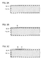
- Fig. 3A is a schematic cross-sectional view of the main portion showing a process of producing the recording head according to Embodiment 1.
- Fig. 3B is a schematic cross-sectional view of the main portion showing the process of producing the recording head according to Embodiment 1.
- Fig. 3C is a schematic cross-sectional view of the main portion showing the process of producing the recording head according to Embodiment 1.
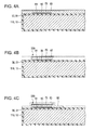
- Fig. 4A is a schematic cross-sectional view of the main portion showing the process of producing the recording head according to Embodiment 1.
- Fig. 4B is a schematic cross-sectional view of the main portion showing the process of producing the recording head according to Embodiment 1.
- Fig. 4C is a schematic cross-sectional view of the main portion showing the process of producing the recording head according to Embodiment 1.
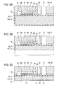
- Fig. 5A is a schematic cross-sectional view of the main portion showing the process of producing the recording head according to Embodiment 1.
- Fig. 5B is a schematic cross-sectional view of the main portion showing the process of producing the recording head according to Embodiment 1.
- Fig. 5C is a schematic cross-sectional view of the main portion showing the process of producing the recording head according to Embodiment 1.
- Fig. 6 is a schematic cross-sectional view of the main portion showing the process of producing the recording head according to Embodiment 1.
- Fig. 7 is an exploded perspective view of a recording head according to Embodiment 2.
- Fig. 8 is a cross-sectional view of the recording head according to Embodiment 2.
- Fig. 9 is a graph showing a relationship between temperature and dielectric constant in Sample 1.
- Fig. 10 is a graph showing a relationship between temperature and dielectric constant in Sample 3.
- Fig. 11 is a graph showing a relationship between temperature and dielectric constant in Sample 6.
- Fig. 12 is a graph showing an X-ray diffraction pattern of Sample 1.
- Fig. 13 is a graph showing an X-ray diffraction pattern of Sample 6.
- Fig. 14 is a perspective view of a liquid ejecting apparatus according to another Embodiment.
- Fig. 1 is an exploded perspective view schematically showing a constitution of an ink jet recording head as an example of the liquid ejecting head according to Embodiment 1 of the invention
- Fig. 2A is a plan view of the ink jet recording head
- Fig. 2B is a cross-sectional view taken along the line IIB-IIB of the plan view.
- an elastic film 50 is disposed on one surface of a flow path-forming substrate 10 of the Embodiment.
- the flow path-forming substrate 10 is made of, for example, a single-crystal silicon substrate having a crystal face preferentially oriented along the (111) plane.
- the term "preferentially oriented along the (111) plane” includes the possibility that all crystals are oriented along the (111) plane and the possibility that most crystals (for example, 90% or more) are oriented along the (111) plane.
- the elastic film 50 is made of, for example, silicon oxide.
- the single-crystal silicon substrate in this Embodiment is preferentially oriented along the (111) plane, but is not limited thereto.
- the flow path-forming substrate 10 is provided with a plurality of pressure generating chambers 12 arranged in parallel in its width direction. Furthermore, the flow path-forming substrate 10 is provided with a communicating portion 13 in an area on an outer side in the longitudinal direction of the pressure generating chambers 12, and the communicating portion 13 and each pressure generating chamber 12 are in communication with each other through an ink-supplying path 14 and a communicating path 15 provided to each of the pressure generating chambers 12.
- the communicating portion 13 communicates with a reservoir portion 31 of a protective substrate described below to constitute a part of a reservoir 100 serving as an ink chamber common to all the pressure generating chambers 12.
- the ink-supplying path 14 has a width which is narrower than that of the pressure generating chamber 12 and maintains a constant flow path resistance of ink flowing in the pressure generating chamber 12 from the communicating portion 13.
- the ink-supplying path 14 is formed by narrowing the width of the flow path from one side, but it may also be formed by narrowing the width of the flow path from both sides. Alternatively, the ink-supplying path may be formed by narrowing the flow path from the thickness direction, instead of narrowing the width of the flow path.
- the flow path-forming substrate 10 is bonded to a nozzle plate 20 with, for example, an adhesive or a thermal adhesive film on the opening surface side.
- the nozzle plate 20 is perforated with nozzle orifices 21 that communicate with the corresponding pressure-generating chambers 12 in the vicinity of the ends of the pressure-generating chambers 12 on the side opposite to the ink-supplying path 14.
- the nozzle plate 20 is made of, for example, a glass ceramic material, a single-crystal silicon substrate, or stainless steel.
- the elastic film 50 is disposed on the opposite side of the flow path-forming substrate 10 relative to the opening surface side.
- a first electrode 60, a piezoelectric layer 70 and a second electrode 80 are laminated to constitute a piezoelectric element 300.
- the piezoelectric layer is a thin film having a thickness of 10 ⁇ m or less, preferably 0.3 to 1.5 ⁇ m.
- the first electrode 60 and the second electrode 80 are made of, for example, platinum (Pt) and are preferentially oriented along the (111) plane.
- an adhesive layer 61 is disposed between the first electrode 60 and the elastic film 50.
- the adhesive layer 61 is not particularly limited as long as it can improve the adhesive force between the lower electrode film 60 and the elastic film 50, and examples thereof are those having a thickness of 10 to 50 nm and containing, as a main component, at least one selected from the group consisting of titanium (Ti), chromium (Cr), tantalum (Ta), zirconium (Zr), and tungsten (W).
- Ti titanium
- Cr chromium
- Ta tantalum
- Zr zirconium
- W tungsten
- the piezoelectric element 300 is a portion including the first electrode 60, the piezoelectric layer 70, and the second electrode 80.
- one of the electrodes of each piezoelectric element 300 is formed as a common electrode, and the other electrode and the piezoelectric layer 70 are formed by patterning for each pressure-generating chamber 12.
- the first electrode 60 is the common electrode of the piezoelectric elements 300
- the second electrode 80 is the individual electrode of each piezoelectric element 300, but these may be reversed depending on a driving circuit or wiring.
- the piezoelectric element 300 when disposed so as to be displaceable, may be referred to as an actuator.
- the piezoelectric layer 70 disposed on the first electrode 60 is a perovskite-type oxide comprising barium titanate (for example, BaTiO 3 ), calcium titanate (for example, CaTiO 3 ) and europium oxide (for example, Eu 2 O 3 ).
- the piezoelectric layer 70 contains barium titanate as a main component (for example, 90% or more of the entire piezoelectric layer 70) and further contains calcium titanate and europium oxide (for example, 2 to 10% and 0.1 to 5%, respectively, of the entire piezoelectric layer 70).
- the piezoelectric layer 70 thus contains barium titanate, calcium titanate, and europium oxide
- the piezoelectric element 300 is capable of withstanding high voltages and also has good displacement characteristics.
- the ink jet recording head I is useful in practice. The details will be described below.
- the piezoelectric layer 70 further comprises zirconium oxide (for example, ZrO 2 ). By containing zirconium oxide, the displacement characteristics are further improved.
- the piezoelectric layer 70 comprises, for example, barium titanate, calcium titanate, europium oxide, and zirconium oxide in a weight ratio of 0.93 to 0.95:0.05 to 0.07:0.005 to 0.01:0.005 to 0.01, which is represented by the following formula (1): x[BaTiO 3 ]-(1-x)[CaTiO 3 ]-y[Eu 2 O 3 ]-z[ZrO 2 ] (1) (wherein, 0.93 ⁇ x ⁇ 0.95, 0.005 ⁇ y ⁇ 0.01, 0.005 ⁇ z ⁇ 0.01). Note that when zirconium oxide is not contained, z is zero in the formula (1).
- the perovskite-type oxide is a compound having a perovskite structure.
- the perovskite structure that is, in the ABO 3 structure, twelve oxygen atoms are coordinated to the A-site, and six oxygen atoms are coordinated to the B-site to form an octahedron.
- Ba, Ca, and Bu are located at the A-site, and Ti and, according to need, Zr are located at the B-site.
- Eu is located at the A-site where Ba is located
- Zr is located at the B-site where Ti is located.
- the ionic radii of Ba and Eu are respectively 149 pm and 95 pm; thus, Ba and Eu are significantly different in their ionic radii.
- the ionic radii of Ti and Zr are respectively 75 pm and 86 pm; Ti and Zr are also significantly different in their ionic radii. Therefore, it is assumed that the parent crystal lattice is deformed by the inclusion of Eu and Zr at respectively the A-site and the B-site of the crystal lattice. This deformation is assumed to allow every rotation of a domain, resulting in an improvement in the piezoelectric properties (i.e. displacement characteristics of the material).
- the second electrode 80 serving as the individual electrode of the piezoelectric element 300 is connected to a lead electrode 90 made of, for example, gold (Au) that is drawn out from the vicinity of the end on the ink-supplying path 14 side of the second electrode 80 and extends on the elastic film 50.
- a lead electrode 90 made of, for example, gold (Au) that is drawn out from the vicinity of the end on the ink-supplying path 14 side of the second electrode 80 and extends on the elastic film 50.
- a protective substrate 30 is provided above the flow path-forming substrate 10 provided with piezoelectric elements 300. That is, the protective substrate 30 is bonded to the first electrode 60, the elastic film 50, and the lead electrodes 90 with an adhesive 35.
- the protective substrate 30 has a reservoir portion 31 which constitutes at least a part of the reservoir 100.
- the reservoir portion 31 is formed along the width direction of the pressure generating chambers 12 so as to pass through the protective substrate 30 in the thickness direction and communicates with the communicating portion 13 of the flow path-forming substrate 10 to constitute the reservoir 100 serving as a common ink chamber for the pressure generating chambers 12, as described above.
- the communicating portion 13 of the flow path-forming substrate 10 may be divided so as to correspond to each pressure generating chamber 12, and only the reservoir portion 31 may serve as the reservoir 100.
- the flow path-forming substrate 10 may be provided with only the pressure generating chambers 12, and members (for example, the elastic film 50) interposed between the flow path-forming substrate 10 and the protective substrate 30 may be provided with the reservoir 100 and the ink-supplying paths 14 communicating with the corresponding pressure generating chambers 12.
- the protective substrate 30 is provided with a piezoelectric element holding portion 32 at an area facing the piezoelectric elements 300.
- the piezoelectric element holding portion 32 has a space that is enough not to prevent the movement of the piezoelectric elements 300.
- the space of the piezoelectric element holding portion 32 may be sealed or not be sealed as long as it is enough not to prevent the movement of the piezoelectric elements 300.
- the protective substrate 30 is preferably made of a material having almost the same coefficient of thermal expansion as that of the flow path-forming substrate 10, for example, glass or a ceramic material.
- the protective substrate 30 is a single-crystal silicon substrate, which is the same material as that of the flow path-forming substrate 10.
- the protective substrate 30 is provided with a through-hole 33 passing through the protective substrate 30 in the thickness direction.
- the through-hole 33 is formed so that the vicinity of the end of the lead electrode 90 drawn out from each piezoelectric element 300 is exposed in the through-hole 33.
- a driving circuit 120 for driving the piezoelectric elements 300 arranged in parallel is fixed on the protective substrate 30.
- the driving circuit 120 may be, for example, a circuit board or a semiconductor integrated circuit (IC).
- the driving circuit 120 and the lead electrodes 90 are electrically connected to each other through connecting wire 121 composed of conductive wire such as bonding wire.
- a compliance substrate 40 including a sealing film 41 and a fixing plate 42 is bonded on the protective substrate 30.
- the sealing film 41 is formed of a flexible material having a low rigidity and seals one side of the reservoir portion 31.
- the fixing plate 42 is formed of a relatively hard material.
- the fixing plate 42 is provided with an opening 43 at an area corresponding to the reservoir 100 by completely removing the fixing plate 42 in the thickness direction. Therefore, one side of the reservoir 100 is sealed with only the sealing film 41 having flexibility.
- ink is fed through an ink inlet being connected to exterior ink supplying means (not shown) to fill the inside from the reservoir 100 to the nozzle orifices 21 with ink.
- a voltage is applied between the first electrode 60 and the second electrode 80 corresponding to each pressure generating chamber 12 according to a recording signal from the driving circuit 120 to flexurally deform the elastic film 50, the first electrode 60, and the piezoelectric layer 70.
- the pressure in each pressure generating chamber 12 is increased, and ink droplets are discharged from the nozzle orifices 21.
- FIGS. 3A to 3C , 4A to 4C , and 5A to 5C are cross-sectional views showing the process of producing the ink jet recording head of the Embodiment.
- an oxide film 51 constituting the elastic film 50 is formed on a surface of a flow path-forming substrate wafer 110 of a silicon wafer that forms a plurality of flow path-forming substrates 10 in a unified manner.
- the method for forming the oxide film 51 is not particularly limited.
- the flow path-forming substrate wafer 110 is thermally oxidized to form a silicon dioxide film 51 serving as the elastic film 50 on the surface thereof.
- the adhesive layer 61 is formed by any method without particular limitation, but can be formed by, for example, sputtering or chemical vapor deposition (CVD).
- a first electrode 60 made of platinum (Pt) and having a thickness of 50 to 500 nm is formed on the adhesive layer 61.
- the first electrode 60 and the adhesive layer 61 are patterned into a predetermined shape.
- the first electrode 60 may be formed by any method without particular limitation, but can be formed by, for example, sputtering or CVD. In the Embodiment, the first electrode 60 is formed by sputtering. Examples of the patterning include dry etching such as reactive ion etching and ion milling.
- a piezoelectric layer 70 containing barium titanate as a main component and further containing calcium titanate, europium oxide, and, according to need, zirconium oxide is formed.
- the piezoelectric layer 70 is formed by, for example, a sol-gel method, metal organic decomposition (MOD), or sputtering.
- the piezoelectric layer 70 is formed by the sol-gel method. Occurrence of cracking in the piezoelectric layer 70 can be prevented by forming the piezoelectric layer 70 by the sol-gel method using sol of the Embodiment described below, and also the cost can be reduced.
- sol used in the sol-gel method of the Embodiment
- CaTiO 3 sol, Eu 2 O 3 sol, and, according to need, ZrO 2 sol are added to BaTiO 3 sol, and a fine powder composed of BaTiO 3 having an average particle size of 10 to 100 nm is further added thereto.
- a high concentration of BaTiO 3 in the sol can be obtained by adding powdery BaTiO 3 to sol containing metal organic compounds that are usually used for forming the piezoelectric layer 70. By doing so, the solid content is increased, a thick film can be formed, and also the sol hardly shrinks during firing. As a result, stress is reduced to prevent cracking from occurring.
- the sol that is used in the Embodiment preferably contains at least one selected from potassium (K) and silicon (Si) for reducing the crystallization temperature. That is, there has been a problem that the crystallization temperature is high for forming a barium titanate-based thin film, but in the Embodiment, the crystallization temperature can be reduced by adding at least one selected from K and Si to the sol. In this case, each of K and Si can be added in a sol state.
- the above-mentioned sol (solution) is applied on the flow path-forming substrate 10 provided with the first electrode 60 to form a piezoelectric precursor film (application step).
- the thickness is 0.5 to 1.0 ⁇ m.
- the thickness is 1.0 to 2.0 ⁇ m, preferably 1.5 to 2.0 ⁇ m. Since the solid solution content is high and cracking hardly occurs in the piezoelectric layer 70 by forming the film using the sol of the Embodiment, the film can have a large thickness.
- the piezoelectric precursor film is heated at a predetermined temperature for a predetermined time for drying (drying step). For example, in the Embodiment, the drying step is conducted by keeping the film at 150 to 180°C for 2 to 10 minutes.
- the dried piezoelectric precursor film is heated to a predetermined temperature and is kept at the temperature for a predetermined period of time for degreasing (degreasing step).
- the piezoelectric precursor film is heated to about 300 to 450°C and is kept at that temperature for about 2 to 10 minutes for degreasing.
- the term "degreasing" means that organic components contained in the piezoelectric precursor film are eliminated as, for example, NO 2 , CO 2 , or H 2 O.
- the piezoelectric precursor film is heated to a predetermined temperature with an infrared heater and is kept at the temperature for a predetermined period of time for crystallization to form a piezoelectric film (firing step).
- a piezoelectric layer 70 composed of a plurality of layers of piezoelectric films is formed by repeating more than once the piezoelectric film-forming process composed of the application step, the drying step, the degreasing step, and the firing step.
- the above-mentioned sol since the above-mentioned sol is used, cracking hardly occurs. Therefore, a thick piezoelectric precursor film can be formed. Consequently, the number of repetitions of the piezoelectric film-forming process is reduced, and the manufacturing cost can be reduced.
- a second electrode 80 is formed on the piezoelectric layer 70.
- the piezoelectric layer 70 and the second electrode 80 are patterned in areas corresponding to the pressure generating chambers 12 to form piezoelectric elements 300.
- the piezoelectric layer 70 and the second electrode 80 are patterned by, for example, dry etching such as reactive ion etching or ion milling.
- lead electrodes 90 are formed. Specifically, as shown in Fig. 4C , a layer for the lead electrodes 90 made of, for example, gold (Au) is formed on the entire surface of the flow path-forming substrate wafer 110 and then is patterned through a mask pattern (not shown) composed of resist or the like to form the lead electrodes 90 corresponding to the respective piezoelectric elements 300.
- Au gold
- a protective substrate wafer 130 that is a silicon wafer for forming a plurality of protective substrates 30 is bonded to the flow path-forming substrate wafer 11D on the piezoelectric element 300 side with an adhesive 35.
- the flow path-forming substrate wafer 110 is thinned to a predetermined thickness.
- a new mask film 52 is formed on the flow path-forming substrate wafer 110 and patterned into a predetermined shape.
- the flow path-forming substrate wafer 110 is anisotropically etched (wet-etched) with an alkaline solution such as KOH through the mask film 52 to form the pressure generating chambers 12, the communicating portion 13, the ink-supplying paths 14, and the communicating paths 15 corresponding to the respective piezoelectric elements 300.
- the nozzle plate 20 perforated with nozzle orifices 21 is bonded to the flow path-forming substrate wafer 110 on the side opposite to the protective substrate wafer 130.
- the compliance substrate 40 is bonded to the protective substrate wafer 130, and the flow path-forming substrate wafer 110 and other associated components are divided into individual chip-sized flow path-forming substrates 10 and other components as shown in Fig. 1 to give an ink jet recording head I of the Embodiment as shown in Fig. 1 .
- Fig. 7 is an exploded perspective view schematically showing an ink jet recording head as an example of a liquid ejecting head according to Embodiment 2 of the invention
- Fig. 8 is a cross-sectional view of the ink jet recording head.
- the ink jet recording head 510 is constituted of an actuator unit 520, a flow path unit 530 fixed to the actuator unit 520, and a wiring board 550 connected to the actuator unit 520.
- the actuator unit 520 is an actuator including piezoelectric elements 540 and includes a flow path-forming substrate 522 provided with pressure generating chambers 521, a diaphragm 523 disposed on one side of the flow path-forming substrate 522, and a pressure generating chamber bottom plate 524 disposed on the other side of the flow path-forming substrate 522.
- the flow path-forming substrate 522 is, for example, a ceramic plate of alumina (Al 2 O 3 ), zirconia (ZrO 2 ), or the like of about 150 ⁇ m in a thickness and is provided with a plurality of pressure generating chambers 521. In the Embodiment, two rows of the pressure generating chambers 521 arranged in parallel along the width direction thereof are formed.
- the diaphragm 523 is, for example, a zirconia thin plate with a thickness of 10 ⁇ m and is fixed to one side of the flow path-forming substrate 522 and seals the one side of each pressure generating chamber 521.
- the pressure generating chamber bottom plate 524 is fixed to the other side of the flow path-forming substrate 522 to seal the other side of each pressure generating chamber 521.
- the pressure generating chamber bottom plate 524 is provided with supply-communication holes 525 and nozzle-communication holes 526.
- the supply-communication holes 525 are each formed in the vicinity of one end in the longitudinal direction of each pressure generating chamber 521 and communicate between the pressure generating chambers 521 and a reservoir described below.
- the nozzle-communication holes 526 are each formed in the vicinity of the other end in the longitudinal direction of each pressure generating chamber 521 and communicate with nozzle orifices 534 described below.
- the piezoelectric elements 540 are disposed on the diaphragm 523 so as to face the corresponding pressure generating chambers 521 with the diaphragm 523 therebetween.
- the number of rows of the piezoelectric elements 540 is also two.
- each piezoelectric element 540 is constituted of a first electrode (electrode layer) 543 disposed on the diaphragm 523, a piezoelectric layer (piezoelectric ceramic layer) 544 independently disposed so as to correspond to each pressure generating chamber 521, and a second electrode (electrode layer) 545 disposed on each piezoelectric layer 544.
- the piezoelectric layer 544 is usually a thick (for example, 10 to 1000 ⁇ m) layer made of a piezoelectric material and is a bulk piezoelectric layer formed by, for example, a solid phase reaction in which a powder of a metal oxide or a metal carbonate is physically mixed, pulverized, and molded and then being fired.
- the first electrode 543 is formed across the piezoelectric layers 544 arranged in parallel and serves as a common electrode of the piezoelectric elements 540 and functions as a part of the diaphragm.
- the first electrode 543 may be provided to each piezoelectric layer 544.
- the layers constituting the actuator unit 520 i.e., the flow path-forming substrate 522, the diaphragm 523, and the pressure generating chamber bottom plate 524 are formed in a unified manner without using adhesives by molding clay ceramic materials, so-called green sheets, into predetermined thicknesses, forming, for example, pressure generating chambers 521 in them, and then laminating them and firing. Then, the piezoelectric elements 540 are formed on the diaphragm 523.
- the piezoelectric layer 544 formed on the first electrode 543 has a composition similar to that in Embodiment 1 and is a perovskite-type oxide comprising barium titanate, calcium titanate, and europium oxide.
- the piezoelectric layer 544 comprises barium titanate as a main component (for example, 90% or more of the entire piezoelectric layer 544) and further comprises calcium titanate and europium oxide (for example, 2 to 10% and 0.1 to 5%, respectively, of the entire piezoelectric layer 544).
- the piezoelectric layer 544 contains barium titanate, calcium titanate, and europium oxide, the piezoelectric element 300 is capable of withstanding high voltages and also has good displacement characteristics. As a result, the ink jet recording head 510 is useful in practice. The details will be described below.
- the piezoelectric layer 544 further contains zirconium oxide as in Embodiment 1. By containing zirconium oxide, the displacement characteristics are further improved.
- the piezoelectric layer 544 contain barium titanate, calcium titanate, europium oxide, and zirconium oxide in a weight ratio of 0.93 to 0.95:0.05 to 0.07:0.005 to 0.01:0.005 to 0.01, which is represented by the following formula (1): x[BaTiO 3 ]-(1-x)[CaTiO 3 ]-y[Eu 2 O 3 ]-z[ZrO 2 ] (1) (wherein, 0.93 ⁇ x ⁇ 0.95, 0.005 ⁇ y ⁇ 0.01, 0.005 ⁇ z0.01). Note that when zirconium oxide is not contained, z is zero in the formula (1).
- the perovskite-type oxide is a compound having a perovskite structure.
- the perovskite structure that is, in the RBO 3 structure, twelve oxygen atoms are coordinated to the A-site, and six oxygen atoms are coordinated to the B-site to form an octahedron.
- Ba, Ca, and Eu are located at the A-site, and Ti and, according to need, Zr are located at the B-site.
- Eu is located at the A-site where Ba is located, and Zr is located at the B-site where Ti is located.
- the ionic radii of Ba and Eu are respectively 149 pm and 95 pm; Ba and Eu are significantly different in their ionic radii.
- the ionic radii of Ti and Zr are respectively 75 pm and 86 pm; Ti and Zr are also significantly different in their ionic radii. Therefore, it is assumed that the parent crystal lattice is deformed by the inclusion of Eu and Zr at respectively the A-site and the B-site of the crystal lattice. This deformation is assumed to allow easy rotation of a domain, resulting in an improvement in the piezoelectric properties (i.e. displacement characteristics of the material).
- the flow path unit 530 is composed of an ink supply aperture-forming substrate 531 that is bonded to the pressure generating chamber bottom plate 524 of the actuator unit 520, a reservoir-forming substrate 533 provided with a reservoir 532 that serves as a common ink chamber of a plurality of the pressure generating chambers 521, and a nozzle plate 535 provided with nozzle orifices 534.
- the ink supply aperture-forming substrate 531 is a zirconia thin plate with a thickness of 150 ⁇ m and is perforated with nozzle-communication holes 536 and ink supply apertures 537.
- the nozzle-communication holes 536 connect between the nozzle orifices 534 and the pressure generating chambers 521, and the ink supply apertures 537 connect the supply-communication holes 525 and the pressure generating chambers 521 to a corresponding reservoir 532.
- the ink supply aperture-forming substrate 531 is further provided with ink inlets 538 that communicate with the respective reservoirs 532 and supply ink from an exterior ink tank.
- the reservoir-forming substrate 533 is made of a plate material having corrosion resistance suitable for constituting an ink flow path, for example, stainless steel with a thickness of 150 ⁇ m and is provided with the reservoirs 532 and the nozzle-communication holes 539.
- the reservoir 532 receives ink from an exterior ink tank (not shown) and supplies the ink to the pressure generating chambers 521.
- the nozzle-communication holes 539 connect the pressure generating chambers 521 and the nozzle orifices 534.
- the nozzle plate 535 is made of, for example, a stainless steel thin plate and is perforated with nozzle orifices 534 arranged at the same pitch as that of the pressure generating chambers 521.
- the nozzle plate 535 is bonded to the reservoir-forming substrate 533 on the side opposite to the flow path-forming substrate 522 and seais one side of the reservoir 532.
- the flow path unit 530 is formed by fixing the ink supply aperture-forming substrate 531, the reservoir-forming substrate 533, and the nozzle plate 535 with, for example, an adhesive or a thermal adhesive film.
- the reservoir-forming substrate 533 and the nozzle plate 535 are made of stainless steel, but the flow path unit 530 may be made of, for example, a ceramic material in a unified manner as in the actuator unit 520.
- the flow path unit 530 and the actuator unit 520 are bonded and fixed to each other with, for example, an adhesive or a thermal adhesive film.
- terminal portions 546 communicating with the piezoelectric elements 540 are each provided in an area facing the peripheral wall of each pressure generating chamber 521 at one end in the longitudinal direction of each piezoelectric element 540.
- the terminal portions 546 are provided to the respective piezoelectric elements 540 and are conductively coupled to second electrodes 545 of the piezoelectric elements 540.
- Terminal portions (not shown) that are conducted to the first electrode 543 drawn out to both end sides in the parallel direction of the piezoelectric elements and the terminal portions 546 are arranged in parallel in the arrangement direction of the piezoelectric elements 540.
- two rows of the terminal portions 546 are arranged in parallel between the rows of the piezoelectric elements 540 arranged in parallel.
- the terminal portion 546 is configured so that the height from the flow path-forming substrate 522 (diaphragm 523), i.e., the upper end face is higher than the height of the piezoelectric element 540 from the flow path-forming substrate 522 (diaphragm 523). By doing so, when the terminal portion 546 is connected to the wiring layer of the wiring board 550, the wiring board 550 does not abut against the piezoelectric element 540, and thereby a decrease in displacement of the piezoelectric element 540 can be prevented.
- the height of the terminal portion 546 from the flow path-forming substrate 522 (diaphragm 523) is designed to be 20 ⁇ m.
- the terminal portion 546 can be formed by, for example, screen-printing a highly conductive metal material such as silver (Ag).
- the terminal portion that is conductively coupled to each second electrode 545 and first electrode 543 of the piezoelectric element 540 is electrically connected to the wiring layer 551 provided to the wiring board 550, and thereby a driving signal from a driving circuit (not shown) is supplied to each piezoelectric element 540 via the wiring board 550.
- the driving circuit is not shown in the drawing, but may be mounted on the wiring board 550 or may be mounted on a component other than the wiring board 550.
- the wiring board 550 is formed of, for example, one flexible printing circuit (FPC) or one tape carrier package (TCP) provided across the two rows of the piezoelectric elements 540.
- the wiring board 550 is formed, for example, by that a wiring layer 551 having a predetermined pattern is formed on a surface of a base film 552 made of polyimide or the like by subjecting the surface to, for example, tin plating using a copper thin film as a base, and the wiring layer 551 is covered with an insulating material 553 such as resist at the area other than the end that is connected to the terminal portion 546.
- FPC flexible printing circuit
- TCP tape carrier package
- the wiring board 550 is provided with a through-hole 554 in an area between the rows of the piezoelectric elements 540 arranged in parallel.
- the wiring layer 551 is connected to the terminal portion 546 at the end on the through-hole 554 side.
- a wiring layer 551 that is connected to the piezoelectric elements 540 in one row and a wiring layer 551 that is connected to the piezoelectric elements 540 in the other row are formed on a surface of a base film 552 that is not yet provided with the through-hole 554 so that the wiring layers 551 are continuous, and then the through-hole 554 of the wiring board 550 is formed in the base film 552 so that the conductively coupled wiring layers 551 that are connected to the two rows of the piezoelectric elements 540 are divided.
- the wiring layer 551 of the wiring board 550 and the terminal portion conductively coupled to the piezoelectric element 540 are connected electrically and mechanically via an adhesive layer 555 made of an anisotropic conductive material.
- ink is fed into the reservoir 532 from an ink cartridge (storage means) through the ink inlet 538 to fill the liquid flow path from the reservoir 532 to the nozzle orifices 534 with the ink.
- a recording signal from a driving circuit (not shown) is supplied to each piezoelectric element 540 through the wiring board 550 to apply a voltage to the piezoelectric element 540 corresponding to each pressure generating chamber 521 and thereby flexurally deform the piezoelectric element 540 and also the diaphragm 523.
- the pressure in each pressure generating chamber 521 is increased to eject ink droplets from each nozzle orifice 534.
- the piezoelectric layer 544 for example, powders of BaCO 3 , TiO 2 , Eu 2 O 3 , and, according to need, ZrO 2 are prepared. These powders in dried states are weighed at a predetermined ratio and then are mixed and pulverized, for example, in a ball mill containing pure water or ethanol to give a raw material mixture.
- the raw material mixture is dried and then synthesized (calcined), for example, at 900 to 1100°C when powders of BaCO 3 , TiO 2 , and Eu 2 O 3 are used and at 1000 to 1200°C when powders of BaCO 3 , TiO 2 , Eu 2 O 3 , and ZrO 2 are used to form a powder containing BaTiO 3 , Eu 2 O 3 , and ZrO 2 .
- a CaTiO 3 solution (sol) is added to the resulting powder, and the mixture is mixed, for example, in a ball mill.
- the resulting mixture is dried and then degreased at about 400 to 600°C when powders of BaCO 3 , TiO 2 , and Eu 2 O 3 are used and at about 600 to 700°C when powders of BaCO 3 , TiO 2 , Eu 2 O 3 , and ZrO 2 are used.
- the degreased mixture is pulverized into a powder.
- a predetermined amount of a binder is added to the resulting powder, followed by granulation and molding at a predetermined pressure (for example, 1000 to 2000 kg/cm 2 ) by die pressing.
- the molded product is sintered at a temperature of about 1000 to 1400°C to form a so-called bulk piezoelectric material consisting of BaTiO 3 -CaTiO 3 -Eu 2 O 3 or BaTiO 3 -CaTiO 3 -Eu 2 O 3 -ZrO 2 .
- the piezoelectric material is ground, and a first electrode 543 and a second electrode 545 are formed on both surfaces thereof. Then, through polling and various types of measurements, the piezoelectric elements 540 are formed. The resulting piezoelectric elements 540 are mounted on a flow path-forming substrate 522 to give an ink jet recording head of the Embodiment. That is, by thus forming the piezoelectric elements 540, an ink jet recording head that is environment friendly and can satisfactorily eject ink droplets regardless of a change in temperature can be achieved.
- a calcium titanate solution is added to a powder containing barium titanate, europium oxide, and, according to need, ZrO 2 , That is, both solid phase reaction and liquid phase reaction are employed so that a calcium titanate solution is added during a process of producing a piezoelectric material.
- a calcium titanate solution is added during a process of producing a piezoelectric material.
- calcium titanate may be added in its powder state as a starting material.
- Sample 1 An aqueous solution of 7% by weight of polyvinyl alcohol (PVA) was added to a BaTiO 3 powder, followed by granulation and then molding at a pressure of 1500 kg/cm 2 by die pressing. The molded product was sintered at 1350°C for 4 hours to obtain Sample 1.
- the resulting Sample 1 was a piezoelectric layer represented by the above-mentioned formula (1) with values of x, y, and z shown in Table 1.
- Sample 2 An aqueous solution of 7% by weight of polyvinyl alcohol (PVA) was added to a BaTiO 3 powder, followed by granulation and then molding at a pressure of 1500 kg/cm 2 by die pressing. The molded product was sintered at 1350°C for 4 hours to obtain Sample 1.
- the resulting Sample 1 was a piezoelectric layer represented by the above-mentioned formula (1) with values of x, y, and z shown in Table 1.
- Powders of BaCO 3 and TiO 2 in dried states were weighed, and ethanol and other components were added thereto, followed by mixing and pulverizing in a ball mill to give a raw material mixture. Then, the raw material mixture was dried and calcined at 1000°C to form a powder of BaTiO 3 .
- a CaTiO 3 solution (sol) was added to the resulting BaTiO 3 powder so that a mixture ratio (weight ratio) of BaTiO 3 and CaTiO 3 is 95:5, followed by mixing.
- the resulting mixture was degreased at 650°C for 1 hour.
- the degreased mixture was pulverized to a powder.
- an aqueous solution of 7% by weight of PVA was added to the resulting powder, followed by granulation and then molding at a pressure of 1500 kg/cm 2 by die pressing.
- the molded product was sintered at 1350°C for 4 hours to obtain Sample 2.
- the resulting Sample 2 was a piezoelectric layer represented by the above-mentioned formula (1) with values of x, y, and z shown in Table 1.
- Samples 1 to 8 were each measured for piezoelectric constant d 33 (displacement characteristics) in the polarization direction, dielectric loss (tan ⁇ ), density, phase transition temperature (To-t) of the crystalline state and Curie temperature (Tc).
- the results are shown in Table 1 and drawings.
- the d 33 was measured with a piezo d 33 meter, a product of UK PIEZOTEST, the tan ⁇ was measured with HP4294A, a product of Hewlett-Packard, and the density was measured by an Archimedes' method.
- the phase transition temperature was determined by measuring dielectric constant ⁇ r with an automatic-recording dielectric constant measurement system (LCR meter) while varying the temperature.
- the some measurement results showing the relationship between dielectric constant and temperature are shown in Fig. 9 (Sample 1), Fig. 10 (Sample 3), and Fig. 11 (Sample 6).
- the displacement characteristics of Samples 6 to 8 further containing ZrO 2 , in addition to BaTiO 3 , CaTiO 3 , and Eu 2 O 3 were further improved compared to Samples 4 and 5 not containing ZrO 2 .
- the d 33 value of Sample 6 was improved by about 10% compared to that of Sample 4 having the same composition ratio as that of Sample 6 except that ZrO 2 is not contained.
- the d 33 value of Sample 8 was improved by about 10% compared to that of Sample 5 having the same composition ratio as that of Sample 8 except that ZrO 2 is not contained.
- the values of d 33 of Samples 7 and 8 look slightly small. This is because their densities are nearly 10% smaller than those of Samples 1 to 6.
- the values d 33 thereof become approximately the same as that of Sample 6 by adjusting the densities to a similar level to those of Samples 1 to 6 by, for example, lengthening the firing time.
- the temperature characteristics were improved. Specifically, as shown in Figs. 9 to 11 , the system of BaTiO 3 and the systems containing CaTiO 3 , Eu 2 O 3 , and ZrO 2 in BaTiO 3 were hardly different in the Curie temperature Tc.
- the phase transition temperature (To-t) of the crystalline state specifically, the temperature at which phase transition occurs from an orthorhombic crystal to a tetragonal crystal, is observed as a peak in dielectric constant measurement, and in Sample 1 ( Fig. 9 ), the To-t peak was observed at room temperature (approximately 19°C).
- Samples 2 to 7 each had a sufficiently low dielectric loss (tan ⁇ ) and were therefore excellent in durability.
- X-ray diffraction patterns of powders of Samples 1 to 8 were obtained with "D8 Discover", a product of Bruker AXS, using CuK ⁇ -ray as a X-ray source at room temperature.
- Fig. 12 (Sample 1) and Fig. 13 (Sample 6) show some of the results. As shown in the results, in all Samples 1 to 7, ABO 3 structures were formed, and no peaks caused by other different phases were observed.
- the piezoelectric layer 70 in Embodiment 1 is produced by a chemical solution method such as a sol-gel method or MOD in which a piezoelectric precursor film formed by application of a piezoelectric precursor solution is crystallized by heating or a gas phase method such as sputtering, but may be a bulk piezoelectric layer formed by a solid phase reaction as the piezoelectric layer 544 of Embodiment 2.
- the piezoelectric layer 544 of Embodiment 2 may be a piezoelectric layer formed by a chemical solution method or a gas phase method as the piezoelectric layer 70 of Embodiment 1.
- the flow path-forming substrate 10 is a single-crystal silicon substrate or a ceramic plate, but is not limited thereto and may be, for example, an SOI substrate or a glass substrate.
- the piezoelectric element is formed by sequentially laminating a first electrode, a piezoelectric layer, and a second electrode on a substrate, but is not limited thereto.
- the invention can be applied to, for example, a longitudinal vibration-type piezoelectric element that extends and contracts in the axial direction by alternately laminating a piezoelectric material and an electrode-forming material.
- the ink jet recording heads of these Embodiments each constitutes a part of a recording head unit including an ink flow path that communicates with, for example, an ink cartridge and is mounted on an ink jet recording apparatus.
- Fig. 14 is a schematic view showing an example of such an ink jet recording apparatus.
- the recording head units 1A and 1B including the ink jet recording heads I are detachably provided with cartridges 2A and 23 constituting ink supplying means.
- the recording head units 1A and 1B are mounted on a carriage 3.
- the carriage 3 is set to a carriage axis 5 that is fixed to an apparatus body 4 in a manner that the carriage 3 is movable in the axial direction.
- the recording head units 1A and 1B discharge, for example, a black ink composition and a color ink composition, respectively.
- Driving force of a driving motor 6 is transferred to the carriage 3 through a plurality of gears (not shown) and a timing belt 7, and thereby the carriage 3, on which the recording head units 1A and 1B are mounted, is moved along the carriage axis 5.
- the apparatus body 4 is provided with a platen 8 along the carriage axis 5, and a recording sheet S, serving as a recording medium such as paper, is fed by, for example, a feeding roller (not shown) and is wrapped around the platen 8 and thereby transported.
- the ink jet recording heads have been described as examples of the liquid ejecting head, but the present invention broadly covers general liquid ejecting heads and also can be applied to liquid ejecting heads that eject liquid other than ink.
- the other liquid ejecting heads include recording heads used in image recording apparatuses such as printers, coloring material ejecting heads used for producing color filters of, for example, liquid crystal displays, electrode material ejecting heads used for forming electrodes of, for example, organic EL displays or field emission displays (FEDs), and bio-organic material ejecting heads used for producing bio-chips.
- the invention is not limited to piezoelectric actuators used in liquid ejecting heads represented by ink jet recording heads and can be applied to other piezoelectric elements, for example, ultrasonic devices such as ultrasonic transmitters, pressure sensors, and ultrasonic motors.
Abstract
A piezoelectric element comprising a piezoelectric layer and a pair of electrodes, wherein
the piezoelectric layer comprises a perovskite-type oxide formed from barium titanate, calcium titanate, and europium oxide.
the piezoelectric layer comprises a perovskite-type oxide formed from barium titanate, calcium titanate, and europium oxide.
Description
- The present invention relates to a piezoelectric element, a liquid ejecting head comprising said piezoelectric element and a liquid ejecting apparatus comprising said head.
- As typical examples of liquid ejecting heads, ink jet recording heads are known. In such ink jet recording heads, a diaphragm constitutes a part of a pressure-generating chamber that communicates with a nozzle orifice for discharging ink drops, and a piezoelectric element deforms the diaphragm to pressurize ink in the pressure-generating chamber and thereby to discharge ink droplets through the nozzle orifice. In some of piezoelectric elements used in the ink jet recording heads, a piezoelectric layer made of a piezoelectric material exhibiting an electromechanical transducing function, such as piezoelectric ceramics, is disposed between two electrodes. Such a piezoelectric element is mounted on a liquid ejecting head as a flexure-vibration-mode actuator.
- In some liquid ejecting heads, lead zirconate titanate (PZT) having high displacement characteristics is used as a piezoelectric ceramic (see
JP-A-2001-223404 JP-A-2000-72539 - However, the piezoelectric property of BaTiO3 is not sufficient for this material to be used as the piezoelectric element of a liquid ejecting head, and therefore further improved materials are required. Accordingly, for example, it has been proposed to improve withstand-voltage characteristics by adding calcium titanate (CaTiO3) to barium titanate (BaTiO3) (for example, see
JP-A-6-279110 - However, even when BaTiO3 to which CaTiO3 is added is used in a piezoelectric element, the displacement characteristics of the element is insufficient. Using these materials, and ink jet recording head cannot be provided with sufficient ejection characteristics.
- An advantage of some aspects of the invention is to provide a piezoelectric element that is less harmful to the environment while having high displacement characteristics. Also provided are a liquid ejecting head comprising the piezoelectric element and a liquid ejecting apparatus having the liquid ejecting head.
- According to a first aspect of the invention a piezoelectric element comprising a piezoelectric layer and a pair of electrodes, wherein the piezoelectric layer comprises a perovskite-type oxide comprising barium titanate, calcium titanate, and europium oxide is provided. Since the piezoelectric layer includes barium titanate, calcium titanate, and europium oxide, the element is relatively environmentally friendly. The displacement characteristics are high. Therefore, the element, can be used in a liquid ejecting head to provide sufficient ejection characteristics.
- It is preferable that the piezoelectric layer further comprises potassium (K) or silicon (Si). Since the crystallization temperature can be reduced by containing K or Si, the piezoelectric layer can be formed at a lower temperature.
- It is preferable that the piezoelectric layer further comprises zirconium oxide. By doing so, the displacement characteristics are further improved.
- It is preferable that the perovskite-type oxide is represented by the following Formula (1):
x[BaTiO3]-(1-x)[CaTiO3]-y[Eu2O3]-z[ZrO2] (1)
(wherein, 0.93≤x≤0.95, 0.005≤y≤0.01, 0.005≤z≤0.01).
By doing so, the displacement characteristics can be certainly improved. - According to a second aspect of the invention, a liquid ejecting head comprising the piezoelectric element defined in the first embodiment above is provided.
- According to a third aspect of the invention, a liquid ejecting apparatus is provided which comprises the liquid ejecting head defined in the second embodiment above. Since the liquid ejecting apparatus has the liquid ejecting head including the piezoelectric element that has a reduced environmental load and also high displacement characteristics, the liquid ejecting apparatus can be reduced in environmental load and provided with high liquid ejection performance.
- The invention will be described with reference to the accompanying drawings, wherein like numbers reference like elements.
-
Fig. 1 is an exploded perspective view of a recording head according toEmbodiment 1. -
Fig. 2A is a plan view of the recording head according to Embodiment 1. -
Fig. 2B is a cross-sectional view of the recording head according toEmbodiment 1. -
Fig. 3A is a schematic cross-sectional view of the main portion showing a process of producing the recording head according toEmbodiment 1. -
Fig. 3B is a schematic cross-sectional view of the main portion showing the process of producing the recording head according toEmbodiment 1. -
Fig. 3C is a schematic cross-sectional view of the main portion showing the process of producing the recording head according toEmbodiment 1. -
Fig. 4A is a schematic cross-sectional view of the main portion showing the process of producing the recording head according toEmbodiment 1. -
Fig. 4B is a schematic cross-sectional view of the main portion showing the process of producing the recording head according toEmbodiment 1. -
Fig. 4C is a schematic cross-sectional view of the main portion showing the process of producing the recording head according toEmbodiment 1. -
Fig. 5A is a schematic cross-sectional view of the main portion showing the process of producing the recording head according toEmbodiment 1. -
Fig. 5B is a schematic cross-sectional view of the main portion showing the process of producing the recording head according toEmbodiment 1. -
Fig. 5C is a schematic cross-sectional view of the main portion showing the process of producing the recording head according toEmbodiment 1. -
Fig. 6 is a schematic cross-sectional view of the main portion showing the process of producing the recording head according toEmbodiment 1. -
Fig. 7 is an exploded perspective view of a recording head according to Embodiment 2. -
Fig. 8 is a cross-sectional view of the recording head according to Embodiment 2. -
Fig. 9 is a graph showing a relationship between temperature and dielectric constant inSample 1. -
Fig. 10 is a graph showing a relationship between temperature and dielectric constant inSample 3. -
Fig. 11 is a graph showing a relationship between temperature and dielectric constant in Sample 6. -
Fig. 12 is a graph showing an X-ray diffraction pattern ofSample 1. -
Fig. 13 is a graph showing an X-ray diffraction pattern of Sample 6. -
Fig. 14 is a perspective view of a liquid ejecting apparatus according to another Embodiment. -
Fig. 1 is an exploded perspective view schematically showing a constitution of an ink jet recording head as an example of the liquid ejecting head according toEmbodiment 1 of the invention, andFig. 2A is a plan view of the ink jet recording head, andFig. 2B is a cross-sectional view taken along the line IIB-IIB of the plan view. - As shown in
Figs. 1 ,2A, and 2B , anelastic film 50 is disposed on one surface of a flow path-formingsubstrate 10 of the Embodiment. The flow path-formingsubstrate 10 is made of, for example, a single-crystal silicon substrate having a crystal face preferentially oriented along the (111) plane. In the invention, the term "preferentially oriented along the (111) plane" includes the possibility that all crystals are oriented along the (111) plane and the possibility that most crystals (for example, 90% or more) are oriented along the (111) plane. Theelastic film 50 is made of, for example, silicon oxide. The single-crystal silicon substrate in this Embodiment is preferentially oriented along the (111) plane, but is not limited thereto. - The flow path-forming
substrate 10 is provided with a plurality ofpressure generating chambers 12 arranged in parallel in its width direction. Furthermore, the flow path-formingsubstrate 10 is provided with a communicatingportion 13 in an area on an outer side in the longitudinal direction of thepressure generating chambers 12, and the communicatingportion 13 and eachpressure generating chamber 12 are in communication with each other through an ink-supplyingpath 14 and a communicatingpath 15 provided to each of thepressure generating chambers 12. The communicatingportion 13 communicates with areservoir portion 31 of a protective substrate described below to constitute a part of areservoir 100 serving as an ink chamber common to all thepressure generating chambers 12. The ink-supplyingpath 14 has a width which is narrower than that of thepressure generating chamber 12 and maintains a constant flow path resistance of ink flowing in thepressure generating chamber 12 from the communicatingportion 13. In the Embodiment which is shown, the ink-supplyingpath 14 is formed by narrowing the width of the flow path from one side, but it may also be formed by narrowing the width of the flow path from both sides. Alternatively, the ink-supplying path may be formed by narrowing the flow path from the thickness direction, instead of narrowing the width of the flow path. - In addition, the flow path-forming
substrate 10 is bonded to anozzle plate 20 with, for example, an adhesive or a thermal adhesive film on the opening surface side. Thenozzle plate 20 is perforated withnozzle orifices 21 that communicate with the corresponding pressure-generatingchambers 12 in the vicinity of the ends of the pressure-generatingchambers 12 on the side opposite to the ink-supplyingpath 14. Thenozzle plate 20 is made of, for example, a glass ceramic material, a single-crystal silicon substrate, or stainless steel. - Furthermore, as described above, the
elastic film 50 is disposed on the opposite side of the flow path-formingsubstrate 10 relative to the opening surface side. On theelastic film 50, afirst electrode 60, apiezoelectric layer 70 and asecond electrode 80 are laminated to constitute apiezoelectric element 300. the piezoelectric layer is a thin film having a thickness of 10 µm or less, preferably 0.3 to 1.5 µm. Thefirst electrode 60 and thesecond electrode 80 are made of, for example, platinum (Pt) and are preferentially oriented along the (111) plane. Furthermore, anadhesive layer 61 is disposed between thefirst electrode 60 and theelastic film 50. Theadhesive layer 61 is not particularly limited as long as it can improve the adhesive force between thelower electrode film 60 and theelastic film 50, and examples thereof are those having a thickness of 10 to 50 nm and containing, as a main component, at least one selected from the group consisting of titanium (Ti), chromium (Cr), tantalum (Ta), zirconium (Zr), and tungsten (W). By providing anadhesive layer 61 between thefirst electrode 60 and theelastic film 50, the adhesive force between theelastic film 50 and thefirst electrode 60 can be increased. - In this Embodiment, the
piezoelectric element 300 is a portion including thefirst electrode 60, thepiezoelectric layer 70, and thesecond electrode 80. In general, one of the electrodes of eachpiezoelectric element 300 is formed as a common electrode, and the other electrode and thepiezoelectric layer 70 are formed by patterning for each pressure-generatingchamber 12. In the Embodiment, thefirst electrode 60 is the common electrode of thepiezoelectric elements 300, and thesecond electrode 80 is the individual electrode of eachpiezoelectric element 300, but these may be reversed depending on a driving circuit or wiring. Thepiezoelectric element 300, when disposed so as to be displaceable, may be referred to as an actuator. - The
piezoelectric layer 70 disposed on thefirst electrode 60 is a perovskite-type oxide comprising barium titanate (for example, BaTiO3), calcium titanate (for example, CaTiO3) and europium oxide (for example, Eu2O3). Specifically, thepiezoelectric layer 70 contains barium titanate as a main component (for example, 90% or more of the entire piezoelectric layer 70) and further contains calcium titanate and europium oxide (for example, 2 to 10% and 0.1 to 5%, respectively, of the entire piezoelectric layer 70). - In the Embodiment, since the
piezoelectric layer 70 thus contains barium titanate, calcium titanate, and europium oxide, thepiezoelectric element 300 is capable of withstanding high voltages and also has good displacement characteristics. As a result, the ink jet recording head I is useful in practice. The details will be described below. - Known lead-free piezoelectric ceramic materials in which calcium titanate is added to barium titanate are capable of withstanding high voltages but have poor displacement characteristics and, therefore, are not in practice useful as the piezoelectric layer of a piezoelectric element that is mounted on an ink jet recording head. However, in the Embodiment, not only calcium titanate but also europium oxide is added to barium titanate. By further containing europium oxide, the displacement characteristics are improved. In addition, temperature characteristics and durability are satisfactory. In this regard, the details will be described in experimental examples described below.
- It is preferable that the
piezoelectric layer 70 further comprises zirconium oxide (for example, ZrO2). By containing zirconium oxide, the displacement characteristics are further improved. - It is preferable that the
piezoelectric layer 70 comprises, for example, barium titanate, calcium titanate, europium oxide, and zirconium oxide in a weight ratio of 0.93 to 0.95:0.05 to 0.07:0.005 to 0.01:0.005 to 0.01, which is represented by the following formula (1):
x[BaTiO3]-(1-x)[CaTiO3]-y[Eu2O3]-z[ZrO2] (1)
(wherein, 0.93≤x≤0.95, 0.005≤y≤0.01, 0.005≤z≤0.01).
Note that when zirconium oxide is not contained, z is zero in the formula (1). - The perovskite-type oxide is a compound having a perovskite structure. In the perovskite structure, that is, in the ABO3 structure, twelve oxygen atoms are coordinated to the A-site, and six oxygen atoms are coordinated to the B-site to form an octahedron. Ba, Ca, and Bu are located at the A-site, and Ti and, according to need, Zr are located at the B-site.
- In the invention, by adding small amounts of europium oxide and zirconium oxide to barium titanate serving as the main component, Eu is located at the A-site where Ba is located, and Zr is located at the B-site where Ti is located. The ionic radii of Ba and Eu are respectively 149 pm and 95 pm; thus, Ba and Eu are significantly different in their ionic radii. Similarly, the ionic radii of Ti and Zr are respectively 75 pm and 86 pm; Ti and Zr are also significantly different in their ionic radii. Therefore, it is assumed that the parent crystal lattice is deformed by the inclusion of Eu and Zr at respectively the A-site and the B-site of the crystal lattice. This deformation is assumed to allow every rotation of a domain, resulting in an improvement in the piezoelectric properties (i.e. displacement characteristics of the material).
- The
second electrode 80 serving as the individual electrode of thepiezoelectric element 300 is connected to alead electrode 90 made of, for example, gold (Au) that is drawn out from the vicinity of the end on the ink-supplyingpath 14 side of thesecond electrode 80 and extends on theelastic film 50. - Above the flow path-forming
substrate 10 provided withpiezoelectric elements 300, aprotective substrate 30 is provided. That is, theprotective substrate 30 is bonded to thefirst electrode 60, theelastic film 50, and thelead electrodes 90 with an adhesive 35. Theprotective substrate 30 has areservoir portion 31 which constitutes at least a part of thereservoir 100. In the Embodiment, thereservoir portion 31 is formed along the width direction of thepressure generating chambers 12 so as to pass through theprotective substrate 30 in the thickness direction and communicates with the communicatingportion 13 of the flow path-formingsubstrate 10 to constitute thereservoir 100 serving as a common ink chamber for thepressure generating chambers 12, as described above. Alternatively, the communicatingportion 13 of the flow path-formingsubstrate 10 may be divided so as to correspond to eachpressure generating chamber 12, and only thereservoir portion 31 may serve as thereservoir 100. Furthermore, for example, the flow path-formingsubstrate 10 may be provided with only thepressure generating chambers 12, and members (for example, the elastic film 50) interposed between the flow path-formingsubstrate 10 and theprotective substrate 30 may be provided with thereservoir 100 and the ink-supplyingpaths 14 communicating with the correspondingpressure generating chambers 12. - The
protective substrate 30 is provided with a piezoelectricelement holding portion 32 at an area facing thepiezoelectric elements 300. The piezoelectricelement holding portion 32 has a space that is enough not to prevent the movement of thepiezoelectric elements 300. The space of the piezoelectricelement holding portion 32 may be sealed or not be sealed as long as it is enough not to prevent the movement of thepiezoelectric elements 300. - The
protective substrate 30 is preferably made of a material having almost the same coefficient of thermal expansion as that of the flow path-formingsubstrate 10, for example, glass or a ceramic material. In the Embodiment, theprotective substrate 30 is a single-crystal silicon substrate, which is the same material as that of the flow path-formingsubstrate 10. - The
protective substrate 30 is provided with a through-hole 33 passing through theprotective substrate 30 in the thickness direction. The through-hole 33 is formed so that the vicinity of the end of thelead electrode 90 drawn out from eachpiezoelectric element 300 is exposed in the through-hole 33. - Furthermore, a driving
circuit 120 for driving thepiezoelectric elements 300 arranged in parallel is fixed on theprotective substrate 30. The drivingcircuit 120 may be, for example, a circuit board or a semiconductor integrated circuit (IC). The drivingcircuit 120 and thelead electrodes 90 are electrically connected to each other through connectingwire 121 composed of conductive wire such as bonding wire. - In addition, a
compliance substrate 40 including a sealingfilm 41 and a fixingplate 42 is bonded on theprotective substrate 30. Here, the sealingfilm 41 is formed of a flexible material having a low rigidity and seals one side of thereservoir portion 31. The fixingplate 42 is formed of a relatively hard material. The fixingplate 42 is provided with anopening 43 at an area corresponding to thereservoir 100 by completely removing the fixingplate 42 in the thickness direction. Therefore, one side of thereservoir 100 is sealed with only the sealingfilm 41 having flexibility. - In such an ink jet recording head of the Embodiment, ink is fed through an ink inlet being connected to exterior ink supplying means (not shown) to fill the inside from the
reservoir 100 to thenozzle orifices 21 with ink. Then, a voltage is applied between thefirst electrode 60 and thesecond electrode 80 corresponding to eachpressure generating chamber 12 according to a recording signal from the drivingcircuit 120 to flexurally deform theelastic film 50, thefirst electrode 60, and thepiezoelectric layer 70. Thereby, the pressure in eachpressure generating chamber 12 is increased, and ink droplets are discharged from thenozzle orifices 21. - A process of producing the ink jet recording head of the Embodiment will be described with reference to
Figs. 3A to 3C ,4A to 4C , and5A to 5C , which are cross-sectional views showing the process of producing the ink jet recording head of the Embodiment. - First, as shown in
Fig. 3A , an oxide film 51 constituting theelastic film 50 is formed on a surface of a flow path-forming substrate wafer 110 of a silicon wafer that forms a plurality of flow path-formingsubstrates 10 in a unified manner. The method for forming the oxide film 51 is not particularly limited. In the Embodiment, the flow path-forming substrate wafer 110 is thermally oxidized to form a silicon dioxide film 51 serving as theelastic film 50 on the surface thereof. - Then, as shown in
Fig. 3B , anadhesive layer 61 is formed on the oxide film 51. Theadhesive layer 61 may be formed by any method without particular limitation, but can be formed by, for example, sputtering or chemical vapor deposition (CVD). - Then, as shown in
Fig. 3C , afirst electrode 60 made of platinum (Pt) and having a thickness of 50 to 500 nm is formed on theadhesive layer 61. Thefirst electrode 60 and theadhesive layer 61 are patterned into a predetermined shape. Thefirst electrode 60 may be formed by any method without particular limitation, but can be formed by, for example, sputtering or CVD. In the Embodiment, thefirst electrode 60 is formed by sputtering. Examples of the patterning include dry etching such as reactive ion etching and ion milling. - Then, as shown in
Fig. 4A , apiezoelectric layer 70 containing barium titanate as a main component and further containing calcium titanate, europium oxide, and, according to need, zirconium oxide is formed. Thepiezoelectric layer 70 is formed by, for example, a sol-gel method, metal organic decomposition (MOD), or sputtering. In the Embodiment, thepiezoelectric layer 70 is formed by the sol-gel method. Occurrence of cracking in thepiezoelectric layer 70 can be prevented by forming thepiezoelectric layer 70 by the sol-gel method using sol of the Embodiment described below, and also the cost can be reduced. - An example of the sol (solution) used in the sol-gel method of the Embodiment will be described below. In the sol of the Embodiment, CaTiO3 sol, Eu2O3 sol, and, according to need, ZrO2 sol are added to BaTiO3 sol, and a fine powder composed of BaTiO3 having an average particle size of 10 to 100 nm is further added thereto. A high concentration of BaTiO3 in the sol can be obtained by adding powdery BaTiO3 to sol containing metal organic compounds that are usually used for forming the
piezoelectric layer 70. By doing so, the solid content is increased, a thick film can be formed, and also the sol hardly shrinks during firing. As a result, stress is reduced to prevent cracking from occurring. That is, there has been a problem that cracking tends to occur in BaTiO3 thin films, but in the Embodiment, occurrence of cracking can be effectively prevented by adding a powder to the sol. As such a BaTiO3 powder, for example, BT01, a product of Sakai Chemical Industry Co., Ltd., can be used. - Furthermore, the sol that is used in the Embodiment preferably contains at least one selected from potassium (K) and silicon (Si) for reducing the crystallization temperature. That is, there has been a problem that the crystallization temperature is high for forming a barium titanate-based thin film, but in the Embodiment, the crystallization temperature can be reduced by adding at least one selected from K and Si to the sol. In this case, each of K and Si can be added in a sol state.
- The method will be specifically described below. The above-mentioned sol (solution) is applied on the flow path-forming
substrate 10 provided with thefirst electrode 60 to form a piezoelectric precursor film (application step). When the piezoelectric precursor film is a usual PZT film, the thickness is 0.5 to 1.0 µm. However, in the Embodiment, the thickness is 1.0 to 2.0 µm, preferably 1.5 to 2.0 µm. Since the solid solution content is high and cracking hardly occurs in thepiezoelectric layer 70 by forming the film using the sol of the Embodiment, the film can have a large thickness. Then, the piezoelectric precursor film is heated at a predetermined temperature for a predetermined time for drying (drying step). For example, in the Embodiment, the drying step is conducted by keeping the film at 150 to 180°C for 2 to 10 minutes. - Then, the dried piezoelectric precursor film is heated to a predetermined temperature and is kept at the temperature for a predetermined period of time for degreasing (degreasing step). For example, in the Embodiment, the piezoelectric precursor film is heated to about 300 to 450°C and is kept at that temperature for about 2 to 10 minutes for degreasing. In the specification, the term "degreasing" means that organic components contained in the piezoelectric precursor film are eliminated as, for example, NO2, CO2, or H2O. Then, the piezoelectric precursor film is heated to a predetermined temperature with an infrared heater and is kept at the temperature for a predetermined period of time for crystallization to form a piezoelectric film (firing step).
- A
piezoelectric layer 70 composed of a plurality of layers of piezoelectric films is formed by repeating more than once the piezoelectric film-forming process composed of the application step, the drying step, the degreasing step, and the firing step. In the Embodiment, since the above-mentioned sol is used, cracking hardly occurs. Therefore, a thick piezoelectric precursor film can be formed. Consequently, the number of repetitions of the piezoelectric film-forming process is reduced, and the manufacturing cost can be reduced. - Then, as shown in
Fig. 4A , asecond electrode 80 is formed on thepiezoelectric layer 70. Subsequently, as shown inFig. 4B , thepiezoelectric layer 70 and thesecond electrode 80 are patterned in areas corresponding to thepressure generating chambers 12 to formpiezoelectric elements 300. Thepiezoelectric layer 70 and thesecond electrode 80 are patterned by, for example, dry etching such as reactive ion etching or ion milling. - Then, lead
electrodes 90 are formed. Specifically, as shown inFig. 4C , a layer for thelead electrodes 90 made of, for example, gold (Au) is formed on the entire surface of the flow path-forming substrate wafer 110 and then is patterned through a mask pattern (not shown) composed of resist or the like to form thelead electrodes 90 corresponding to the respectivepiezoelectric elements 300. - Then, as shown in
Fig. 5A , a protective substrate wafer 130 that is a silicon wafer for forming a plurality ofprotective substrates 30 is bonded to the flow path-forming substrate wafer 11D on thepiezoelectric element 300 side with an adhesive 35. - Then, as shown in
Fig. 5B , the flow path-forming substrate wafer 110 is thinned to a predetermined thickness. Subsequently, as shown inFig. 5C , anew mask film 52 is formed on the flow path-forming substrate wafer 110 and patterned into a predetermined shape. Then, as shown inFig. 6 , the flow path-forming substrate wafer 110 is anisotropically etched (wet-etched) with an alkaline solution such as KOH through themask film 52 to form thepressure generating chambers 12, the communicatingportion 13, the ink-supplyingpaths 14, and the communicatingpaths 15 corresponding to the respectivepiezoelectric elements 300. - Then, unneeded portions at the outer peripheries of the flow path-forming substrate wafer 110 and the protective substrate wafer 138 are removed by cutting, e.g., by dicing. The
nozzle plate 20 perforated withnozzle orifices 21 is bonded to the flow path-forming substrate wafer 110 on the side opposite to the protective substrate wafer 130. Thecompliance substrate 40 is bonded to the protective substrate wafer 130, and the flow path-forming substrate wafer 110 and other associated components are divided into individual chip-sized flow path-formingsubstrates 10 and other components as shown inFig. 1 to give an ink jet recording head I of the Embodiment as shown inFig. 1 . -
Fig. 7 is an exploded perspective view schematically showing an ink jet recording head as an example of a liquid ejecting head according to Embodiment 2 of the invention, andFig. 8 is a cross-sectional view of the ink jet recording head. - As shown in the drawings, the ink
jet recording head 510 is constituted of anactuator unit 520, aflow path unit 530 fixed to theactuator unit 520, and awiring board 550 connected to theactuator unit 520. - The
actuator unit 520 is an actuator includingpiezoelectric elements 540 and includes a flow path-formingsubstrate 522 provided withpressure generating chambers 521, adiaphragm 523 disposed on one side of the flow path-formingsubstrate 522, and a pressure generatingchamber bottom plate 524 disposed on the other side of the flow path-formingsubstrate 522. - The flow path-forming
substrate 522 is, for example, a ceramic plate of alumina (Al2O3), zirconia (ZrO2), or the like of about 150 µm in a thickness and is provided with a plurality ofpressure generating chambers 521. In the Embodiment, two rows of thepressure generating chambers 521 arranged in parallel along the width direction thereof are formed. Thediaphragm 523 is, for example, a zirconia thin plate with a thickness of 10 µm and is fixed to one side of the flow path-formingsubstrate 522 and seals the one side of eachpressure generating chamber 521. - The pressure generating
chamber bottom plate 524 is fixed to the other side of the flow path-formingsubstrate 522 to seal the other side of eachpressure generating chamber 521. The pressure generatingchamber bottom plate 524 is provided with supply-communication holes 525 and nozzle-communication holes 526. The supply-communication holes 525 are each formed in the vicinity of one end in the longitudinal direction of eachpressure generating chamber 521 and communicate between thepressure generating chambers 521 and a reservoir described below. The nozzle-communication holes 526 are each formed in the vicinity of the other end in the longitudinal direction of eachpressure generating chamber 521 and communicate withnozzle orifices 534 described below. - The
piezoelectric elements 540 are disposed on thediaphragm 523 so as to face the correspondingpressure generating chambers 521 with thediaphragm 523 therebetween. For example, in the Embodiment, since the number of rows of thepressure generating chambers 521 is two, the number of rows of thepiezoelectric elements 540 is also two. - In the Embodiment, each
piezoelectric element 540 is constituted of a first electrode (electrode layer) 543 disposed on thediaphragm 523, a piezoelectric layer (piezoelectric ceramic layer) 544 independently disposed so as to correspond to eachpressure generating chamber 521, and a second electrode (electrode layer) 545 disposed on eachpiezoelectric layer 544. In the Embodiment, thepiezoelectric layer 544 is usually a thick (for example, 10 to 1000 µm) layer made of a piezoelectric material and is a bulk piezoelectric layer formed by, for example, a solid phase reaction in which a powder of a metal oxide or a metal carbonate is physically mixed, pulverized, and molded and then being fired. Thefirst electrode 543 is formed across thepiezoelectric layers 544 arranged in parallel and serves as a common electrode of thepiezoelectric elements 540 and functions as a part of the diaphragm. Thefirst electrode 543 may be provided to eachpiezoelectric layer 544. - The layers constituting the
actuator unit 520, i.e., the flow path-formingsubstrate 522, thediaphragm 523, and the pressure generatingchamber bottom plate 524 are formed in a unified manner without using adhesives by molding clay ceramic materials, so-called green sheets, into predetermined thicknesses, forming, for example,pressure generating chambers 521 in them, and then laminating them and firing. Then, thepiezoelectric elements 540 are formed on thediaphragm 523. - The
piezoelectric layer 544 formed on thefirst electrode 543 has a composition similar to that inEmbodiment 1 and is a perovskite-type oxide comprising barium titanate, calcium titanate, and europium oxide. Specifically, thepiezoelectric layer 544 comprises barium titanate as a main component (for example, 90% or more of the entire piezoelectric layer 544) and further comprises calcium titanate and europium oxide (for example, 2 to 10% and 0.1 to 5%, respectively, of the entire piezoelectric layer 544). Thus, in also this Embodiment as inEmbodiment 1, since thepiezoelectric layer 544 contains barium titanate, calcium titanate, and europium oxide, thepiezoelectric element 300 is capable of withstanding high voltages and also has good displacement characteristics. As a result, the inkjet recording head 510 is useful in practice. The details will be described below. - Known lead-free piezoelectric ceramic materials in which calcium titanate is added to barium titanate are capable of withstanding high voltages but have poor displacement characteristics and, therefore, are not in practice useful as the piezoelectric layer of the piezoelectric element that is mounted on an ink jet recording head. However, in the Embodiment, not only calcium titanate but also europium oxide is added to barium titanate. By further containing europium oxide, the displacement characteristics are improved. In addition, temperature characteristics and durability are satisfactory. In this regard, the details will be described in experimental examples described below.
- Furthermore, it is preferable that the
piezoelectric layer 544 further contains zirconium oxide as inEmbodiment 1. By containing zirconium oxide, the displacement characteristics are further improved. - It is preferable that the
piezoelectric layer 544 contain barium titanate, calcium titanate, europium oxide, and zirconium oxide in a weight ratio of 0.93 to 0.95:0.05 to 0.07:0.005 to 0.01:0.005 to 0.01, which is represented by the following formula (1):
x[BaTiO3]-(1-x)[CaTiO3]-y[Eu2O3]-z[ZrO2] (1)
(wherein, 0.93≤x≤0.95, 0.005≤y≤0.01, 0.005≤z0.01).
Note that when zirconium oxide is not contained, z is zero in the formula (1). - The perovskite-type oxide is a compound having a perovskite structure. In the perovskite structure, that is, in the RBO3 structure, twelve oxygen atoms are coordinated to the A-site, and six oxygen atoms are coordinated to the B-site to form an octahedron. Ba, Ca, and Eu are located at the A-site, and Ti and, according to need, Zr are located at the B-site.
- In the invention, by adding small amounts of europium oxide and zirconium oxide to barium titanate serving as the main component, Eu is located at the A-site where Ba is located, and Zr is located at the B-site where Ti is located. The ionic radii of Ba and Eu are respectively 149 pm and 95 pm; Ba and Eu are significantly different in their ionic radii. Similarly, the ionic radii of Ti and Zr are respectively 75 pm and 86 pm; Ti and Zr are also significantly different in their ionic radii. Therefore, it is assumed that the parent crystal lattice is deformed by the inclusion of Eu and Zr at respectively the A-site and the B-site of the crystal lattice. This deformation is assumed to allow easy rotation of a domain, resulting in an improvement in the piezoelectric properties (i.e. displacement characteristics of the material).
- The process of producing the
piezoelectric element 540 having such apiezoelectric layer 544 will be described in detail below. - The
flow path unit 530 is composed of an ink supply aperture-formingsubstrate 531 that is bonded to the pressure generatingchamber bottom plate 524 of theactuator unit 520, a reservoir-formingsubstrate 533 provided with areservoir 532 that serves as a common ink chamber of a plurality of thepressure generating chambers 521, and anozzle plate 535 provided withnozzle orifices 534. - The ink supply aperture-forming
substrate 531 is a zirconia thin plate with a thickness of 150 µm and is perforated with nozzle-communication holes 536 andink supply apertures 537. The nozzle-communication holes 536 connect between thenozzle orifices 534 and thepressure generating chambers 521, and theink supply apertures 537 connect the supply-communication holes 525 and thepressure generating chambers 521 to acorresponding reservoir 532. The ink supply aperture-formingsubstrate 531 is further provided withink inlets 538 that communicate with therespective reservoirs 532 and supply ink from an exterior ink tank. - The reservoir-forming
substrate 533 is made of a plate material having corrosion resistance suitable for constituting an ink flow path, for example, stainless steel with a thickness of 150 µm and is provided with thereservoirs 532 and the nozzle-communication holes 539. Thereservoir 532 receives ink from an exterior ink tank (not shown) and supplies the ink to thepressure generating chambers 521. The nozzle-communication holes 539 connect thepressure generating chambers 521 and thenozzle orifices 534. - The
nozzle plate 535 is made of, for example, a stainless steel thin plate and is perforated withnozzle orifices 534 arranged at the same pitch as that of thepressure generating chambers 521. For example, in the Embodiment, since theflow path unit 530 is provided with two rows of the pressure generating chambers, two rows of thenozzle orifices 534 are formed in thenozzle plate 535. Thenozzle plate 535 is bonded to the reservoir-formingsubstrate 533 on the side opposite to the flow path-formingsubstrate 522 and seais one side of thereservoir 532. - The
flow path unit 530 is formed by fixing the ink supply aperture-formingsubstrate 531, the reservoir-formingsubstrate 533, and thenozzle plate 535 with, for example, an adhesive or a thermal adhesive film. In the Embodiment, the reservoir-formingsubstrate 533 and thenozzle plate 535 are made of stainless steel, but theflow path unit 530 may be made of, for example, a ceramic material in a unified manner as in theactuator unit 520. - Then, the
flow path unit 530 and theactuator unit 520 are bonded and fixed to each other with, for example, an adhesive or a thermal adhesive film. - Furthermore, as shown in
Fig. 8 ,terminal portions 546 communicating with thepiezoelectric elements 540 are each provided in an area facing the peripheral wall of eachpressure generating chamber 521 at one end in the longitudinal direction of eachpiezoelectric element 540. Theterminal portions 546 are provided to the respectivepiezoelectric elements 540 and are conductively coupled tosecond electrodes 545 of thepiezoelectric elements 540. Terminal portions (not shown) that are conducted to thefirst electrode 543 drawn out to both end sides in the parallel direction of the piezoelectric elements and theterminal portions 546 are arranged in parallel in the arrangement direction of thepiezoelectric elements 540. In the Embodiment, two rows of theterminal portions 546 are arranged in parallel between the rows of thepiezoelectric elements 540 arranged in parallel. - The
terminal portion 546 is configured so that the height from the flow path-forming substrate 522 (diaphragm 523), i.e., the upper end face is higher than the height of thepiezoelectric element 540 from the flow path-forming substrate 522 (diaphragm 523). By doing so, when theterminal portion 546 is connected to the wiring layer of thewiring board 550, thewiring board 550 does not abut against thepiezoelectric element 540, and thereby a decrease in displacement of thepiezoelectric element 540 can be prevented. In the Embodiment, the height of theterminal portion 546 from the flow path-forming substrate 522 (diaphragm 523) is designed to be 20 µm. - The
terminal portion 546 can be formed by, for example, screen-printing a highly conductive metal material such as silver (Ag). - Furthermore, the terminal portion that is conductively coupled to each
second electrode 545 andfirst electrode 543 of thepiezoelectric element 540 is electrically connected to thewiring layer 551 provided to thewiring board 550, and thereby a driving signal from a driving circuit (not shown) is supplied to eachpiezoelectric element 540 via thewiring board 550. The driving circuit is not shown in the drawing, but may be mounted on thewiring board 550 or may be mounted on a component other than thewiring board 550. - The
wiring board 550 is formed of, for example, one flexible printing circuit (FPC) or one tape carrier package (TCP) provided across the two rows of thepiezoelectric elements 540. Specifically, thewiring board 550 is formed, for example, by that awiring layer 551 having a predetermined pattern is formed on a surface of abase film 552 made of polyimide or the like by subjecting the surface to, for example, tin plating using a copper thin film as a base, and thewiring layer 551 is covered with an insulatingmaterial 553 such as resist at the area other than the end that is connected to theterminal portion 546. - The
wiring board 550 is provided with a through-hole 554 in an area between the rows of thepiezoelectric elements 540 arranged in parallel. Thewiring layer 551 is connected to theterminal portion 546 at the end on the through-hole 554 side. Awiring layer 551 that is connected to thepiezoelectric elements 540 in one row and awiring layer 551 that is connected to thepiezoelectric elements 540 in the other row are formed on a surface of abase film 552 that is not yet provided with the through-hole 554 so that the wiring layers 551 are continuous, and then the through-hole 554 of thewiring board 550 is formed in thebase film 552 so that the conductively coupled wiring layers 551 that are connected to the two rows of thepiezoelectric elements 540 are divided. - Then, the
wiring layer 551 of thewiring board 550 and the terminal portion conductively coupled to thepiezoelectric element 540 are connected electrically and mechanically via anadhesive layer 555 made of an anisotropic conductive material. - In the ink
jet recording head 510 with such a configuration, ink is fed into thereservoir 532 from an ink cartridge (storage means) through theink inlet 538 to fill the liquid flow path from thereservoir 532 to thenozzle orifices 534 with the ink. Then, a recording signal from a driving circuit (not shown) is supplied to eachpiezoelectric element 540 through thewiring board 550 to apply a voltage to thepiezoelectric element 540 corresponding to eachpressure generating chamber 521 and thereby flexurally deform thepiezoelectric element 540 and also thediaphragm 523. As a result, the pressure in eachpressure generating chamber 521 is increased to eject ink droplets from eachnozzle orifice 534. - An example of a process of producing the ink jet recording head of the Embodiment will be described, but the steps other than the step of producing the piezoelectric element are similar to or the same as those in
Embodiment 1, and therefore the descriptions thereof are omitted. - First, as starting materials of main components for obtaining the
piezoelectric layer 544, for example, powders of BaCO3, TiO2, Eu2O3, and, according to need, ZrO2 are prepared. These powders in dried states are weighed at a predetermined ratio and then are mixed and pulverized, for example, in a ball mill containing pure water or ethanol to give a raw material mixture. Subsequently, the raw material mixture is dried and then synthesized (calcined), for example, at 900 to 1100°C when powders of BaCO3, TiO2, and Eu2O3 are used and at 1000 to 1200°C when powders of BaCO3, TiO2, Eu2O3, and ZrO2 are used to form a powder containing BaTiO3, Eu2O3, and ZrO2. - Then, a CaTiO3 solution (sol) is added to the resulting powder, and the mixture is mixed, for example, in a ball mill. The resulting mixture is dried and then degreased at about 400 to 600°C when powders of BaCO3, TiO2, and Eu2O3 are used and at about 600 to 700°C when powders of BaCO3, TiO2, Eu2O3, and ZrO2 are used. Subsequently, the degreased mixture is pulverized into a powder. A predetermined amount of a binder is added to the resulting powder, followed by granulation and molding at a predetermined pressure (for example, 1000 to 2000 kg/cm2) by die pressing. The molded product is sintered at a temperature of about 1000 to 1400°C to form a so-called bulk piezoelectric material consisting of BaTiO3-CaTiO3-Eu2O3 or BaTiO3-CaTiO3-Eu2O3-ZrO2.
- Then, the piezoelectric material is ground, and a
first electrode 543 and asecond electrode 545 are formed on both surfaces thereof. Then, through polling and various types of measurements, thepiezoelectric elements 540 are formed. The resultingpiezoelectric elements 540 are mounted on a flow path-formingsubstrate 522 to give an ink jet recording head of the Embodiment. That is, by thus forming thepiezoelectric elements 540, an ink jet recording head that is environment friendly and can satisfactorily eject ink droplets regardless of a change in temperature can be achieved. - In particular, in the Embodiment, a calcium titanate solution is added to a powder containing barium titanate, europium oxide, and, according to need, ZrO2, That is, both solid phase reaction and liquid phase reaction are employed so that a calcium titanate solution is added during a process of producing a piezoelectric material. By doing so, the capability of the material to withstand high voltages and the piezoelectric properties of the
piezoelectric layer 544 can be further improved. However, calcium titanate may be added in its powder state as a starting material. - The displacement characteristics and other characteristics of the thus produced
piezoelectric layer 544 will be described in detail with reference to the following experimental examples. - An aqueous solution of 7% by weight of polyvinyl alcohol (PVA) was added to a BaTiO3 powder, followed by granulation and then molding at a pressure of 1500 kg/cm2 by die pressing. The molded product was sintered at 1350°C for 4 hours to obtain
Sample 1. The resultingSample 1 was a piezoelectric layer represented by the above-mentioned formula (1) with values of x, y, and z shown in Table 1. Sample 2 - Powders of BaCO3 and TiO2 in dried states were weighed, and ethanol and other components were added thereto, followed by mixing and pulverizing in a ball mill to give a raw material mixture. Then, the raw material mixture was dried and calcined at 1000°C to form a powder of BaTiO3.
- Then, a CaTiO3 solution (sol) was added to the resulting BaTiO3 powder so that a mixture ratio (weight ratio) of BaTiO3 and CaTiO3 is 95:5, followed by mixing. The resulting mixture was degreased at 650°C for 1 hour. Subsequently, the degreased mixture was pulverized to a powder. As in
Sample 1, an aqueous solution of 7% by weight of PVA was added to the resulting powder, followed by granulation and then molding at a pressure of 1500 kg/cm2 by die pressing. The molded product was sintered at 1350°C for 4 hours to obtain Sample 2. The resulting Sample 2 was a piezoelectric layer represented by the above-mentioned formula (1) with values of x, y, and z shown in Table 1. - The same procedure as in Sample 2 was conducted except that the mixture ratio (weight ratio) of BaTiO3 and CaTiO3 was 93:7 instead of 95:5.
- The same procedure as in
Sample 3 was conducted except that a raw material mixture prepared by weighing powders of BaCO3, TiO2, and Eu2O3 in dried states so that the weight ratio of Eu2O3 relative to the total amount of BaTiO3 and CaTiO3 was 0.5% and then mixing and pulverizing the powders in a ball mill containing ethanol and other components and that the sintering temperature was 1300°C. - The same procedure as in Sample 4 was conducted except that the weight ratio of Eu2O3 relative to the total amount of BaTiO3 and CaTiO3 was 1%.
- The same procedure as in Sample 4 was conducted except that a raw material mixture prepared by weighing powders of BaCO3, TiO2, Eu2O3, and ZrO2 in dried states so that the weight ratios of Eu2O3 and ZrO2 relative to the total amount of BaTiO3 and CaTiO3 were each 0.5% and then mixing and pulverizing the powders in a ball mill containing ethanol and other components and that the sintering temperature was 1350°C.
- The same procedure as in Sample 6 was conducted except that the weight ratio of ZrO2 relative to the total amount of BaTiO3 and CaTiO3 was 1% and that the sintering temperature was 1400°C.
- The same procedure as in
Sample 5 was conducted except that a raw material mixture prepared by weighing powders of BaCO3, TiO2, Eu2O3, and ZrO2 in dried states so that the weight ratios of Eu2O3 and ZrO2 relative to the total amount of BaTiO3 and CaTiO3 were 1% and 0.5%, respectively, and then mixing and pulverizing the powders in a ball mill containing ethanol and other components and that the sintering temperature was 1400°C. - The thus formed
Samples 1 to 8 were each measured for piezoelectric constant d33 (displacement characteristics) in the polarization direction, dielectric loss (tan δ), density, phase transition temperature (To-t) of the crystalline state and Curie temperature (Tc). The results are shown in Table 1 and drawings. Here, the d33 was measured with a piezo d33 meter, a product of UK PIEZOTEST, the tan δ was measured with HP4294A, a product of Hewlett-Packard, and the density was measured by an Archimedes' method. The phase transition temperature was determined by measuring dielectric constant εr with an automatic-recording dielectric constant measurement system (LCR meter) while varying the temperature. The some measurement results showing the relationship between dielectric constant and temperature are shown inFig. 9 (Sample 1),Fig. 10 (Sample 3), andFig. 11 (Sample 6). - The results show that
Samples 2 and 3 containing CaTiO3 in BaTiO3 each had a significantly low d33 value compared to that ofSample 1 containing only BaTiO3 and that the values ofSamples 4 and 5 further containing Eu2O3 were 209 pC/N and 182 pC/N, respectively. Therefore, it was confirmed that displacement characteristics are improved by further adding Eu2O3. - Furthermore, the displacement characteristics of Samples 6 to 8 further containing ZrO2, in addition to BaTiO3, CaTiO3, and Eu2O3 were further improved compared to
Samples 4 and 5 not containing ZrO2. Specifically, the d33 value of Sample 6 was improved by about 10% compared to that of Sample 4 having the same composition ratio as that of Sample 6 except that ZrO2 is not contained. Similarly, the d33 value ofSample 8 was improved by about 10% compared to that ofSample 5 having the same composition ratio as that ofSample 8 except that ZrO2 is not contained. Incidentally, the values of d33 ofSamples Samples 1 to 6. The values d33 thereof become approximately the same as that of Sample 6 by adjusting the densities to a similar level to those ofSamples 1 to 6 by, for example, lengthening the firing time. - In addition, the temperature characteristics were improved. Specifically, as shown in
Figs. 9 to 11 , the system of BaTiO3 and the systems containing CaTiO3, Eu2O3, and ZrO2 in BaTiO3 were hardly different in the Curie temperature Tc. On the other hand, as shown in Table 1 andFigs. 9 to 11 , the phase transition temperature (To-t) of the crystalline state, specifically, the temperature at which phase transition occurs from an orthorhombic crystal to a tetragonal crystal, is observed as a peak in dielectric constant measurement, and in Sample 1 (Fig. 9 ), the To-t peak was observed at room temperature (approximately 19°C). However, in Samples 2 to 7, no To-t peaks were observed even at approximately -30°C. Therefore, it was confirmed that the To-t levels of Samples 2 to 7 were lower than -30°C. Here, as shown inFigs. 9 to 11 , the characteristics such as the dielectric constant were not affected by temperature in the temperature range between Tc and To-t. Therefore, inSamples 1 to 7 having approximately the same Tc levels, the characteristics of Samples 2 to 7 having low To-t levels were hardly affected by temperature. Thus, it was confirmed that Samples 2 to 7 were piezoelectric layers having satisfactory temperature characteristics. - In addition, Samples 2 to 7 each had a sufficiently low dielectric loss (tan δ) and were therefore excellent in durability.
- X-ray diffraction patterns of powders of
Samples 1 to 8 were obtained with "D8 Discover", a product of Bruker AXS, using CuKα-ray as a X-ray source at room temperature.Fig. 12 (Sample 1) andFig. 13 (Sample 6) show some of the results. As shown in the results, in allSamples 1 to 7, ABO3 structures were formed, and no peaks caused by other different phases were observed. -
[Table 1] x y z Density (g/cm3) tan δ (%) d33 (pC/N) To-t (°C) Sample 11.0 0 0 5.9 4.0 253 19 Sample 2 0.95 0 0 5.79 1.2 179 <-30 Sample 30.93 0 0 5.75 0.9 152 <-30 Sample 4 0.93 0.005 0 5.72 1.1 209 <-30 Sample 50.93 0.01 0 5.77 1.44 182 <-30 Sample 6 0.93 0.005 0.005 5.7 1.0 229 <-30 Sample 70.93 0.005 0.01 5.32 1.7 202 <-30 Sample 80.93 0.01 0.005 5.38 1.5 196 <-30 - Hereinbefore, the Embodiments of the invention are described, but the basic constitution of the invention is not limited thereto. For example, the
piezoelectric layer 70 inEmbodiment 1 is produced by a chemical solution method such as a sol-gel method or MOD in which a piezoelectric precursor film formed by application of a piezoelectric precursor solution is crystallized by heating or a gas phase method such as sputtering, but may be a bulk piezoelectric layer formed by a solid phase reaction as thepiezoelectric layer 544 of Embodiment 2. Thepiezoelectric layer 544 of Embodiment 2 may be a piezoelectric layer formed by a chemical solution method or a gas phase method as thepiezoelectric layer 70 ofEmbodiment 1. - Furthermore, in the above-described Embodiments, the flow path-forming
substrate 10 is a single-crystal silicon substrate or a ceramic plate, but is not limited thereto and may be, for example, an SOI substrate or a glass substrate. - In addition, in the above-described Embodiments, the piezoelectric element is formed by sequentially laminating a first electrode, a piezoelectric layer, and a second electrode on a substrate, but is not limited thereto. The invention can be applied to, for example, a longitudinal vibration-type piezoelectric element that extends and contracts in the axial direction by alternately laminating a piezoelectric material and an electrode-forming material.
- The ink jet recording heads of these Embodiments each constitutes a part of a recording head unit including an ink flow path that communicates with, for example, an ink cartridge and is mounted on an ink jet recording apparatus.
Fig. 14 is a schematic view showing an example of such an ink jet recording apparatus. - In the ink jet ejecting apparatus II shown in
Fig. 14 , therecording head units cartridges 2A and 23 constituting ink supplying means. Therecording head units carriage 3. Thecarriage 3 is set to acarriage axis 5 that is fixed to an apparatus body 4 in a manner that thecarriage 3 is movable in the axial direction. Therecording head units - Driving force of a driving motor 6 is transferred to the
carriage 3 through a plurality of gears (not shown) and atiming belt 7, and thereby thecarriage 3, on which therecording head units carriage axis 5. The apparatus body 4 is provided with aplaten 8 along thecarriage axis 5, and a recording sheet S, serving as a recording medium such as paper, is fed by, for example, a feeding roller (not shown) and is wrapped around theplaten 8 and thereby transported. - In the above-described embodiments, the ink jet recording heads have been described as examples of the liquid ejecting head, but the present invention broadly covers general liquid ejecting heads and also can be applied to liquid ejecting heads that eject liquid other than ink. Examples of the other liquid ejecting heads include recording heads used in image recording apparatuses such as printers, coloring material ejecting heads used for producing color filters of, for example, liquid crystal displays, electrode material ejecting heads used for forming electrodes of, for example, organic EL displays or field emission displays (FEDs), and bio-organic material ejecting heads used for producing bio-chips.
- Furthermore, the invention is not limited to piezoelectric actuators used in liquid ejecting heads represented by ink jet recording heads and can be applied to other piezoelectric elements, for example, ultrasonic devices such as ultrasonic transmitters, pressure sensors, and ultrasonic motors.
Claims (7)
- A piezoelectric element comprising a piezoelectric layer and a pair of electrodes, wherein
the piezoelectric layer comprises a perovskite-type oxide comprising barium titanate, calcium titanate, and europium oxide. - The piezoelectric element according to Claim 1,
wherein the piezoelectric layer further comprises potassium. - The piezoelectric element according to Claim 1 or 2, wherein the piezoelectric layer further comprises silicon.
- The piezoelectric element according to any of Claims 1 to 3, wherein the piezoelectric layer further comprises zirconium oxide.
- The piezoelectric element according to Claim 4,
wherein the perovskite-type oxide is represented by the following Formula (1):
x[BaTiO3]-(1-x)[CaTiO3]-y[Eu2O3]-z[ZrO2] (1)
(wherein, 0.93x≤x≤0.95, 0.005≤y≤0.01, 0.005≤z≤0.01). - A liquid ejecting head comprising (i) a pressure generating chamber communicating with a nozzle for ejecting liquid droplets and (ii) a piezoelectric element as defined in any preceding claim.
- A liquid ejecting apparatus comprising a liquid ejecting head according to Claim 6.
Applications Claiming Priority (2)
| Application Number | Priority Date | Filing Date | Title |
|---|---|---|---|
| JP2009213782 | 2009-09-15 | ||
| JP2010056802A JP2011086903A (en) | 2009-09-15 | 2010-03-12 | Liquid ejecting head, liquid ejecting apparatus, and piezoelectric element |
Publications (1)
| Publication Number | Publication Date |
|---|---|
| EP2296200A1 true EP2296200A1 (en) | 2011-03-16 |
Family
ID=43242206
Family Applications (1)
| Application Number | Title | Priority Date | Filing Date |
|---|---|---|---|
| EP10176366A Withdrawn EP2296200A1 (en) | 2009-09-15 | 2010-09-13 | Liquid ejecting head, liquid ejecting apparatus, and piezoelectric element |
Country Status (4)
| Country | Link |
|---|---|
| US (1) | US8506058B2 (en) |
| EP (1) | EP2296200A1 (en) |
| JP (1) | JP2011086903A (en) |
| CN (1) | CN102019754A (en) |
Families Citing this family (4)
| Publication number | Priority date | Publication date | Assignee | Title |
|---|---|---|---|---|
| JP2013218259A (en) * | 2012-03-16 | 2013-10-24 | Canon Inc | Dust removing device and imaging device |
| JP5891096B2 (en) * | 2012-04-12 | 2016-03-22 | エスアイアイ・プリンテック株式会社 | Liquid ejecting head manufacturing method, liquid ejecting head, and liquid ejecting apparatus |
| JP5857205B2 (en) * | 2012-09-10 | 2016-02-10 | パナソニックIpマネジメント株式会社 | Line head and inkjet apparatus |
| TWI786907B (en) * | 2021-10-28 | 2022-12-11 | 國立中央大學 | An oscillator frequency modulation method and a piezoelectric structure of oscillator |
Citations (8)
| Publication number | Priority date | Publication date | Assignee | Title |
|---|---|---|---|---|
| JPH06279110A (en) | 1993-03-24 | 1994-10-04 | Central Glass Co Ltd | Barium titanate-containing powdery composition and production of semiconductor porcelain composition using the same |
| JP2000072539A (en) | 1998-08-31 | 2000-03-07 | Kyocera Corp | Piezoelectric material |
| JP2001223404A (en) | 2000-02-08 | 2001-08-17 | Seiko Epson Corp | Piezoelectric element, inkjet recording head, manufacture method thereof |
| JP2003128460A (en) * | 2001-10-23 | 2003-05-08 | Murata Mfg Co Ltd | Piezoelectric ceramics, piezoelectric element and laminated piezoelectric element |
| EP1708211A2 (en) * | 2005-04-01 | 2006-10-04 | TDK Corporation | Multilayer ceramic capacitor based on barium titanate or barium calcium titanate |
| WO2007113280A2 (en) * | 2006-04-03 | 2007-10-11 | Siemens Aktiengesellschaft | Lead-free piezoceramic material comprising the mixed system of alkaline earth perovskite and bismuth metal oxide, and method for producing said material |
| EP1868218A2 (en) * | 2006-06-12 | 2007-12-19 | TDK Corporation | Electronic device, dielectric ceramic composition and the production method |
| WO2009037922A1 (en) * | 2007-09-19 | 2009-03-26 | Murata Manufacturing Co., Ltd. | Dielectric ceramics and laminated ceramic capacitor |
Family Cites Families (3)
| Publication number | Priority date | Publication date | Assignee | Title |
|---|---|---|---|---|
| JP4859333B2 (en) * | 2002-03-25 | 2012-01-25 | セイコーエプソン株式会社 | Manufacturing method of substrate for electronic device |
| JP2006287045A (en) * | 2005-04-01 | 2006-10-19 | Tdk Corp | Electronic component |
| JP2007281031A (en) | 2006-04-03 | 2007-10-25 | Seiko Epson Corp | Actuator device, liquid discharge head and liquid discharge device |
-
2010
- 2010-03-12 JP JP2010056802A patent/JP2011086903A/en active Pending
- 2010-09-10 US US12/879,597 patent/US8506058B2/en active Active
- 2010-09-13 EP EP10176366A patent/EP2296200A1/en not_active Withdrawn
- 2010-09-15 CN CN2010102871102A patent/CN102019754A/en active Pending
Patent Citations (9)
| Publication number | Priority date | Publication date | Assignee | Title |
|---|---|---|---|---|
| JPH06279110A (en) | 1993-03-24 | 1994-10-04 | Central Glass Co Ltd | Barium titanate-containing powdery composition and production of semiconductor porcelain composition using the same |
| JP2000072539A (en) | 1998-08-31 | 2000-03-07 | Kyocera Corp | Piezoelectric material |
| JP2001223404A (en) | 2000-02-08 | 2001-08-17 | Seiko Epson Corp | Piezoelectric element, inkjet recording head, manufacture method thereof |
| JP2003128460A (en) * | 2001-10-23 | 2003-05-08 | Murata Mfg Co Ltd | Piezoelectric ceramics, piezoelectric element and laminated piezoelectric element |
| EP1708211A2 (en) * | 2005-04-01 | 2006-10-04 | TDK Corporation | Multilayer ceramic capacitor based on barium titanate or barium calcium titanate |
| WO2007113280A2 (en) * | 2006-04-03 | 2007-10-11 | Siemens Aktiengesellschaft | Lead-free piezoceramic material comprising the mixed system of alkaline earth perovskite and bismuth metal oxide, and method for producing said material |
| EP1868218A2 (en) * | 2006-06-12 | 2007-12-19 | TDK Corporation | Electronic device, dielectric ceramic composition and the production method |
| WO2009037922A1 (en) * | 2007-09-19 | 2009-03-26 | Murata Manufacturing Co., Ltd. | Dielectric ceramics and laminated ceramic capacitor |
| US20100165541A1 (en) * | 2007-09-19 | 2010-07-01 | Murata Manufacturing Co., Ltd. | Dielectric ceramics, and laminated ceramic capacitor |
Non-Patent Citations (2)
| Title |
|---|
| MAZON T ET AL: "Structural and dielectric properties of Nd3+-doped Ba0.77Ca0.23TiO3 ceramics", JOURNAL OF APPLIED PHYSICS, AMERICAN INSTITUTE OF PHYSICS. NEW YORK, US, vol. 97, no. 10, 16 May 2005 (2005-05-16), pages 104113 - 104113, XP012069401, ISSN: 0021-8979 * |
| YANG Q ET AL: "Structural, electrical, luminescent, and magnetic properties of Ba0.77Ca0.23TiO3:Eu ceramics", MATERIALS CHEMISTRY AND PHYSICS,ELSEVIER, SWITZERLAND, TAIWAN, REPUBLIC OF CHINA, vol. 118, no. 2-3, 15 December 2009 (2009-12-15), pages 484 - 489, XP026703096, ISSN: 0254-0584, Retrieved from the Internet <URL:http://www.sciencedirect.com> [retrieved on 20090912], DOI: 10.1016/j.matchemphys.2009.08.022 * |
Also Published As
| Publication number | Publication date |
|---|---|
| CN102019754A (en) | 2011-04-20 |
| US20110063379A1 (en) | 2011-03-17 |
| JP2011086903A (en) | 2011-04-28 |
| US8506058B2 (en) | 2013-08-13 |
Similar Documents
| Publication | Publication Date | Title |
|---|---|---|
| EP2364853B1 (en) | Liquid ejecting head and liquid ejecting apparatus | |
| EP2364852B1 (en) | Liquid ejecting head, liquid ejecting apparatus using the same, and piezoelectric element | |
| US9799820B2 (en) | Liquid-ejecting head, liquid-ejecting apparatus, piezoelectric element, and piezoelectric material | |
| US9180667B2 (en) | Liquid-ejecting head and liquid-ejecting apparatus | |
| US8690298B2 (en) | Liquid-ejecting head, liquid-ejecting apparatus, and piezoelectric element and piezoelectric material | |
| JP5429492B2 (en) | Liquid ejecting head, liquid ejecting apparatus, piezoelectric element, and actuator device | |
| EP2364851B1 (en) | Liquid ejecting head, liquid ejecting apparatus, and piezoelectric element | |
| US8506058B2 (en) | Liquid ejecting head, liquid ejecting apparatus, and piezoelectric element | |
| EP1705724B1 (en) | Piezoelectric actator and liquid discharging device | |
| US8857952B2 (en) | Liquid ejecting head and liquid ejecting apparatus | |
| JP4812244B2 (en) | Print head | |
| EP1708288A2 (en) | Piezoelectric element, liquid-jet head using piezoelectric element and liquid-jet apparatus | |
| US8783836B2 (en) | Piezoelectric element, liquid ejecting head, and liquid ejecting apparatus | |
| JP2011091234A (en) | Liquid ejection head, liquid ejection device and actuator device | |
| JP2011211140A (en) | Method of manufacturing piezoelectric material, piezoelectric element, liquid ejecting head, and liquid ejecting apparatus | |
| CN101070005B (en) | Actuator, its manufacturing method and printing head | |
| JP2011192951A (en) | Liquid jetting head and liquid jetting apparatus | |
| JP2011066381A (en) | Liquid injection head and liquid injection device using the same |
Legal Events
| Date | Code | Title | Description |
|---|---|---|---|
| PUAI | Public reference made under article 153(3) epc to a published international application that has entered the european phase |
Free format text: ORIGINAL CODE: 0009012 |
|
| AK | Designated contracting states |
Kind code of ref document: A1 Designated state(s): AL AT BE BG CH CY CZ DE DK EE ES FI FR GB GR HR HU IE IS IT LI LT LU LV MC MK MT NL NO PL PT RO SE SI SK SM TR |
|
| AX | Request for extension of the european patent |
Extension state: BA ME RS |
|
| 17P | Request for examination filed |
Effective date: 20110909 |
|
| STAA | Information on the status of an ep patent application or granted ep patent |
Free format text: STATUS: THE APPLICATION HAS BEEN WITHDRAWN |
|
| 18W | Application withdrawn |
Effective date: 20130214 |