EP2290640B1 - Lichtelementdichtmodul und Verfahren dafür - Google Patents
Lichtelementdichtmodul und Verfahren dafür Download PDFInfo
- Publication number
- EP2290640B1 EP2290640B1 EP10173811A EP10173811A EP2290640B1 EP 2290640 B1 EP2290640 B1 EP 2290640B1 EP 10173811 A EP10173811 A EP 10173811A EP 10173811 A EP10173811 A EP 10173811A EP 2290640 B1 EP2290640 B1 EP 2290640B1
- Authority
- EP
- European Patent Office
- Prior art keywords
- led
- seal
- louver
- circuit board
- pliable
- Prior art date
- Legal status (The legal status is an assumption and is not a legal conclusion. Google has not performed a legal analysis and makes no representation as to the accuracy of the status listed.)
- Not-in-force
Links
Images
Classifications
-
- F—MECHANICAL ENGINEERING; LIGHTING; HEATING; WEAPONS; BLASTING
- F21—LIGHTING
- F21V—FUNCTIONAL FEATURES OR DETAILS OF LIGHTING DEVICES OR SYSTEMS THEREOF; STRUCTURAL COMBINATIONS OF LIGHTING DEVICES WITH OTHER ARTICLES, NOT OTHERWISE PROVIDED FOR
- F21V31/00—Gas-tight or water-tight arrangements
- F21V31/005—Sealing arrangements therefor
-
- G—PHYSICS
- G09—EDUCATION; CRYPTOGRAPHY; DISPLAY; ADVERTISING; SEALS
- G09F—DISPLAYING; ADVERTISING; SIGNS; LABELS OR NAME-PLATES; SEALS
- G09F27/00—Combined visual and audible advertising or displaying, e.g. for public address
- G09F27/008—Sun shades, shades, hoods or louvres on electronic displays to minimise the effect of direct sun light on the display
-
- G—PHYSICS
- G09—EDUCATION; CRYPTOGRAPHY; DISPLAY; ADVERTISING; SEALS
- G09F—DISPLAYING; ADVERTISING; SIGNS; LABELS OR NAME-PLATES; SEALS
- G09F9/00—Indicating arrangements for variable information in which the information is built-up on a support by selection or combination of individual elements
- G09F9/30—Indicating arrangements for variable information in which the information is built-up on a support by selection or combination of individual elements in which the desired character or characters are formed by combining individual elements
- G09F9/302—Indicating arrangements for variable information in which the information is built-up on a support by selection or combination of individual elements in which the desired character or characters are formed by combining individual elements characterised by the form or geometrical disposition of the individual elements
- G09F9/3026—Video wall, i.e. stackable semiconductor matrix display modules
-
- G—PHYSICS
- G09—EDUCATION; CRYPTOGRAPHY; DISPLAY; ADVERTISING; SEALS
- G09F—DISPLAYING; ADVERTISING; SIGNS; LABELS OR NAME-PLATES; SEALS
- G09F9/00—Indicating arrangements for variable information in which the information is built-up on a support by selection or combination of individual elements
- G09F9/30—Indicating arrangements for variable information in which the information is built-up on a support by selection or combination of individual elements in which the desired character or characters are formed by combining individual elements
- G09F9/33—Indicating arrangements for variable information in which the information is built-up on a support by selection or combination of individual elements in which the desired character or characters are formed by combining individual elements being semiconductor devices, e.g. diodes
Definitions
- LED display modules incorporate an arrangement of a plurality of different colored LEDs, such as Red-Green-Blue colors known as an LED package.
- the LED package includes a circuit board with the LEDs coupled thereon and extending from the circuit board.
- a potting material is poured over the circuit board, the circuit board is moved into an oven, and the potting material is cured on the circuit board in the oven. The cured potting material isolates and seals the circuit board.
- an ultraviolet protective coating or parylene coating is applied to protect the circuit board.
- Potting and other coatings have a number of drawbacks.
- the materials to pot and coat are heavy and expensive. LED display modules are thereby correspondingly heavy and expensive.
- potting requires multiple manufacturing and handling steps for application to the LED display module.
- the LEDs extending from the circuit board are often bent during the potting process. Bent LEDs either fail entirely or cause inconsistencies in video and picture quality, color and contrast as light from the bent LEDs is readily distinguishable from light generated from LEDs that are properly aligned on the circuit board.
- technicians must manually straighten or replace bent LEDs after manufacture.
- manual correction of bent LEDs can be labor and time extensive, and thereby expensive to the buyer and/or manufacturer. Applying ultraviolet and parylene coatings create similar drawbacks.
- US 2002/0122134 discloses a large format modular video display including a plurality of video image units, each unit sealed against environmental intrusions, including a housing having a front panel and a rear door panel which may be opened for access to the interior.
- a gasket member covers the pixel array of LEDs and includes an array of LED holes in registration with the pixel array so that each LED extends through a respective hole in the gasket.
- the front panel of the housing also includes an array of LED holes so that each pixel group of LEDs may extend through respective holes in the front panel.
- the LED circuit board and front panel are joined by compression with the gasket member sandwiched to seal the LED holes of the front panel against intrusion of weather.
- an LED panel assembly comprising a circuit board including a plurality of LEDs; an LED seal louver coupled over the circuit board, the LED seal louver includes a substrate including one or more substrate cavities, each of the one or more substrate cavities is sized and shaped to loosely receive an LED, a pliable seal membrane coupled with the substrate, the pliable seal membrane includes a pliable material partially extending across the one or more substrate cavities, one or more LED passages extends through the pliable material adjacent to the substrate cavities, each of the LED passages is sized and shaped to receive a single LED, and bulbs for one or more of the plurality of LEDs are correspondingly received within the LED passages, and the pliable material seals around each bulb with an interference fit; and wherein the bulbs for one or more of the plurality of LEDs are visible through the LED seal louver while the pliable seal membrane is sealed around the bulbs, and the LED seal louver seals off the circuit board from an environment exterior to the LED panel assembly.
- a method for making an LED panel assembly comprising forming an LED seal louver including forming a substrate including one or more substrate cavities (300), and coupling a pliable seal membrane with the substrate, the pliable seal membrane extends at least partially across the one or more substrate cavities, and one or more LED passages extend through the pliable seal membrane at the substrate cavities, the one or more LED passages are in a specified pattern; engaging a circuit board including a plurality of LEDs with the LED seal louver including interference fitting one or more LEDs within the one or more LED passages, one LED is interference fit within each LED passage, and the pliable seal membrane forms a seal around a bulb of each interference fit LED, and immobilizing the LEDs interference fit within the LED passages, the LED seal louver retaining the LEDs in the specified pattern with a specified posture.
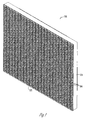
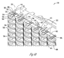
- the LED display module 100 includes an LED display surface 102 configured to provide a color display of graphics and/or video content.
- the LED display surface 102 is surrounded by a display edge seal 104.
- the surface includes a plurality of light emitting elements including light emitting diodes (i.e., LEDs). Each of the light emitting elements is configured to provide light to the LED display surface 102. When multiple light emitting elements 106 are seen together in close proximity various colors are shown by combining the colors of more than one light emitting element.
- the LED display surface 102 includes in one example arrays of light emitting elements 106 each one of the arrays including red, green, and blue light emitting elements that cooperate to provide a spectrum of colors when one, two or three of the light emitting elements in an array are lit.
- the LED display surface 102 is capable of providing a black or empty surface over a portion of the display when necessary by deactivating or turning off the light emitting elements 106 in a particular portion of the LED display surface.
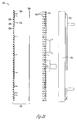
- the LED display module 100 includes a circuit board 200 coupled with a frame 212 to form a first portion of the LED display module.
- An LED seal louver 202 is coupled over top of the light emitting elements 106 to enclose the LED display module 100 thereby sealing out the exterior environment from the interior of the LED display module.
- the LED seal louver 202 is shown in two portions including a substrate 204 and a pliable seal membrane 206. In one example, prior to assembly, the pliable seal membrane 206 is coupled with the substrate 204.
- the pliable seal membrane 206 is over molded onto the substrate 204 thereby making the LED seal louver 202 a unitary structure.
- the LED seal louver 202 includes substrate cavities and LED passages configured to receive light emitting elements 106 in a specified pattern and posture on the circuit board 200.
- the pliable seal membrane 206 tightly engages around each one of the light emitting elements 106 allowing the light emitting elements 106 to project through the LED seal louver 202 while sealing around each one of the light emitting elements to prevent exposure of the interior of the LED display module 100 to the exterior environment.
- the substrate 204 includes, in one example, louver blades 208.
- the louver blades 208 extend at least partially over and under each of the light emitting elements 106 projecting through the LED seal louver 202.
- the louver blades 208 provide a measure of shade to each one of the light emitting elements 106.
- the louver blades 208 thereby assist in preventing interaction of the light emitting elements 106 with sunlight. For instance, glare including sunlight glare off of the light emitting elements 106 interferes with projection of a true color from the light emitting elements. Accurate representation of graphic and video content is frustrated by this interference.
- the shade provided by the louver blades 208 assists in preventing glare from the light emitting elements and additionally allows the light emitting elements to present a true color from a shaded field with minimized interaction with ambient light. Further, provision of the louver blades provides shadow in an area of the LED display surface 102 ( Figure 1 ). When it is desired that a portion of the surface is dark or presents a black surface when video and graphic content are displayed over other portions of the LED display surface, the shade provided by the louver blades 208 assists in ensuring the unlit portion of the surface appears black.
- an edge seal 104 is shown extending around the LED display module 100.
- the display edge seal 104 is shown circumscribing a remainder of the frame 212 when the LED display module 100 is fully assembled.
- the display edge seal 104 extends from the frame 212 into engagement with at least one of the circuit board edge 214 or an LED seal louver edge 216.
- the display edge seal 104 cooperates with the LED seal louver 202 to seal off the components of the LED display module 100 - including the circuit board 200 - from the exterior environment.
- the circuit board 200 is thereby protected from the elements while the light emitting elements 106 project through the LED seal louver 202 for direct visibility through the LED display surface 102. That is to say, protective features including, but not limited to, plastic screening overlays and films placed over the light emitting elements 106 are thereby substantially eliminated allowing the light emitting elements 106 to directly reside on the LED display surface 102 shown in Figure 1 .
- the LED display module 100 includes a frame 212, a circuit board 200 including a plurality of light emitting elements 106, and an LED seal louver 202.
- the LED seal louver 202 includes a substrate 204 and a pliable seal membrane 206 coupled with the substrate.
- the pliable seal membrane 206 is overmolded with the substrate 204 to form a single piece LED seal louver 202 for coupling with the circuit board 200 and the light emitting elements 106.
- the pliable seal membrane 206 is constructed with, but not limited to, a deformable and pliable material such as liquid silicone, rubber, thermoplastic elastomers and the like.
- the pliable seal membrane 206 is deformable to provide a tight interference fit around the light emitting elements 106 when coupled thereto.
- the pliable seal membrane 206 is coupled with the substrate 204, and the substrate 204 provides a rigid frame to support the pliable seal membrane 206 while the LED seal louver 202 is coupled with the light emitting elements 106 and the circuit board 200.
- the substrate 204 is constructed with a material including, but not limited to, polymer, resin, metal and the like.
- the substrate 204 includes polycarbonate, and other similar materials capable of providing a rigid frame to support the pliable seal membrane 206.
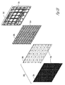
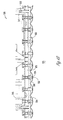
- the circuit board 200 is shown with the light emitting elements 106.
- Each of the light emitting elements extends away from the circuit board 200.
- the light emitting elements 106 extend away in one example with a posture substantially orthogonal to the plane of the circuit board 200. That is to say, each one of the light emitting elements 106 extends away from the circuit board in a substantially consistent posture relative to other light emitting elements 106.
- the light emitting elements 106 are arranged on the circuit board 200 in this posture to ensure each of the elements provides consistent brightness and contrast to the LED display surface 102 shown in Figure 1 .
- the LED seal louver 202 substantially prevents misalignment, bending and the like of the light emitting elements 106 away from the specified posture after coupling with the circuit board 200.
- the light emitting elements 106 shown in Figure 3 include an LED bulb 304 and an LED base 306.
- the LED base 306 includes lead elements soldered with the circuit board 200.
- the light emitting elements 106 are arranged in pixel arrays 314 including, for instance, red, green, and blue light emitting elements in each one of the pixel arrays 314. With the combination of colored light emitting elements each one of the pixel arrays 314 is able to produce a variety of colors for each pixel of the LED display surface 102 ( Figure 1 ).
- the pixel arrays 314 are arranged on the circuit board 200 to provide a specified number of pixels in a specified pattern across an area of the circuit board 200.
- the LED display surface 102 shown in Figure 1 has a corresponding arrangement of pixel arrays 314 because the light emitting elements 106 extend through the LED seal louver 202 in a specified pattern corresponding to the pattern formed on the circuit board 200.
- the LED seal louver 202 shown in Figure 3 includes substrate cavity arrays 316 and LED passage arrays 318 corresponding in arrangement to the pixel array 314 shown on the circuit board 200.
- the LED passages 302 extending through the pliable seal membrane 206 and the substrate cavities 300 extending through the substrate 204 are arranged on the substrate 204 and membrane 206 in a pattern corresponding to the specified pattern formed with the light emitting elements 106 on the circuit board 200.
- the light emitting elements 106 on the circuit board 200 are thereby able to pass through the LED passages 302 and substrate cavities 300 of the LED seal louver 202 in the specified pattern formed on the circuit board 200, and the LED display surface 102 thereby has the pixel array 314 arranged in the circuit board specified pattern.
- the substrate cavities 300 and LED passages 302 are sized and shaped on the respective substrate 204 and pliable seal membrane 206 to align when the membrane and substrate are coupled together to form the LED seal louver 202.
- the substrate cavities 300 are larger than the LED passages 302 and loosely receive the LED bulbs 304.
- the pliable seal membrane 206 is constructed with a pliable material such as silicone.
- the LED passages 302 are sized to provide some degree of interference fit with the light emitting elements 106 when the light emitting elements are passed through the pliable seal membrane 206 of the LED seal louver 202.
- the LED passages provide up to .75 millimeters of interference between the light emitting elements 106 (e.g., LED bulb 304) and the pliable seal membrane 206 surrounding the LED passages 302.
- the pliable seal membrane 206 provides .1 to .45 millimeters interference between the seal membrane material and the light emitting elements 106 when circuit board 200 is coupled with the LED seal louver 202.
- the amount of interference between the pliable seal membrane 206 and the light emitting elements 106 is chosen to ensure tight sealing between the membrane and the light emitting elements over the life of the LED display module 100 ( Figure 1 ) and during the environmental conditions experienced by the LED display module (e.g., cold, hot, damp and dry conditions).
- the LED seal louver 202 tightly seals over each one of the light emitting elements 106.
- the pliable material of the pliable seal membrane 206 surrounding each of the LED passages 302 tightly engages in an interference fit around each of the light emitting elements 106 extending through an LED passage 302.
- the interference fit between the pliable seal membrane 206 of the LED seal louver 202 and the light emitting elements 106 assists in ensuring the circuit board 200 is substantially sealed away from an environment exterior to the LED display module 100.
- Each of the light emitting elements 106 of the pixel arrays 314 extends through the LED seal louver 202 and is directly visible on the LED display surface 102 without any intervening films, plastic screens and the like.
- the louver blade 208 (previously shown in Figure 2 ) are provided to shade each of the light emitting elements 106 extending through the LED seal louver 202.
- the louver blades 208 assist in preventing refraction and reflection of sunlight otherwise incident on the light emitting elements 106.
- the louver blades 208 thereby maintain a consistent contrast and brightness between each one of the light emitting elements 106 providing a consistent LED display surface 102 capable of providing video and graphic content substantially without any variation across the entire display surface.
- the louver blades 208 further provide shade to the light emitting elements 106 when the elements of a particular pixel array 314 are unlit to form a dark or black area on the light emitting display surface 102 ( Figure 1 ).
- the shade provided by the louver blades 208 substantially prevents refraction and reflection of light off of the deactivated light emitting elements 106 to maintain a black appearance to that portion of the LED display surface 102.
- the substrate 204 includes larger substrate cavities 300.
- the substrate cavities 300 are sized and shaped to receive more than one light emitting element 106 in each cavity.
- the pliable seal membrane 206 provides the LED passages 302 shown in Figure 3 thereby ensuring tight engagement between the pliable seal membrane 206 of the LED seal louver 202 and the light emitting elements 106. That is to say, where the substrate 204 includes wider substrate cavities 300 the light emitting elements 106 extend through the LED passages 302 of the pliable seal membrane 206 so that one light emitting element is positioned within each LED passage 302. The light emitting elements 106 project through the substrate 204 and more than one of the light emitting elements 106 is retained in each substrate cavity 300.
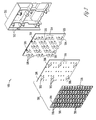
- the pliable seal membrane 206 includes at least one membrane pin cavity 308.
- the circuit board 200 includes at least one circuit board pin cavity 310.
- a positioning pin 210 shown in Figure 2A passes through the membrane pin cavity 308 and circuit board pin cavity 310 when the circuit board 200 is coupled with the LED seal louver 202 so the positioning pins 210 engage with pin sockets 312 formed in the frame 212 (See Figure 3 ).
- the LED seal louver 202 with the positioning pins 210 is thereby able to sandwich the circuit board 200 including the light emitting elements 106 therebetween through coupling of the positioning pins 210 with the pin sockets 312.
- the LED display module 100 includes other coupling features including, but not limited to, screws, bolts, welds, adhesives and the like configured to couple the components of the LED display module together including the frame 212, circuit board 200, and LED seal louver 202.
- FIG. 4A A close up view of the assembled LED display module 100 is shown in Figure 4A .
- the LED seal louver 202 including the substrate204 and pliable seal membrane 206 are coupled with the frame 212 with the circuit board 200 and light emitting elements 106 retained therebetween.
- the light emitting elements 106 including the LED bulbs 304 extend through the substrate cavities 300 of the substrate 204 and LED passages 302 of the pliable seal membrane 206.
- the pliable seal membrane 206 is engaged in an interference fit 414 with the LED bulbs 304.
- the pliable material of the pliable seal membrane 206 deforms as the LED bulbs 304 are pressed through the pliable seal membrane 206.
- the pliable material thereby tightly engages in the interference fit 414 around the LED bulbs 304 creating a seal between the pliable seal membrane and the LED bulbs 304.
- the pliable seal membrane 206 is positioned at an LED seal louver rear side 406. In another example, the pliable seal membrane 206 is positioned on the LED seal louver front side 408.
- the light emitting elements 106 are positioned on the circuit board 200 with the LED bases 306 coupled with the circuit board and the LED bulbs 304 extend from the LED bases.
- the LED bulbs 304 project through the LED seal louver 202 and the LED seal louver is spaced a distance away from the circuit board 200.
- the LED seal louver 202 is spaced from the circuit board 200 according to the size and shape of the positioning pins 210 and pin sockets 312.
- the positioning pins 210 and pin sockets 312 cooperate to ensure the LED seal louver 202 is consistently spaced away from the circuit board 200 and a consistent portion of each light emitting element 106 (e.g., LED bulb 304) extends through the LED seal louver to provide a consistent LED display surface 102 without variations in contrast or brightness.
- the consistent spacing provided by the positioning pins 210 and pin sockets 312 ensure the LED display module 100 has a consistent display across its display surface 102 because each of the light emitting elements 106 of the pixel arrays 314 ( Figure 3 ) are exposed through the LED seal louver 202 in the same manner (e.g., the same length of the bulbs 304 projects from the LED seal louver 202).
- the LED seal louver 202 and the positioning pins 210 cooperate to form an LED support skeleton 412.
- the positioning pins 210 reliably position the LED seal louver 202 over the circuit board 200 and align the light emitting element 106 with the LED passages 302 and substrate cavities 300 of the LED seal louver.
- the LED seal louver 202 is coupled with the circuit board 200 the light emitting elements 106 are guided through the LED passages 302 and the substrate cavities 300 and held therein with the interference fit 414 of the pliable seal membrane 206.
- the pliable seal membrane 206 thereby holds each of the light emitting elements 106 in a specified pattern and specified posture.
- the LED support skeleton 412 holds the light emitting elements 106 in the specified pattern shown in Figure 3 where each of the light emitting elements 106 is positioned on the circuit board 200 in a pixel ray 314.
- the LED seal louver 202 further ensures the light emitting elements 106 are retained in the specified posture, for example, an orthogonal posture relative to the circuit board 200.
- the LED seal louver 202 thereby substantially prevents bending and misalignment of the light emitting elements 106 shown in the LED display surface 102 ( Figure 1 ).
- the positioning pins 210 cooperate with the pin sockets 312 to properly align the LED seal louver 202 on the LED display module 100.
- the LED seal louver 202 When properly aligned the LED seal louver 202 provides a framework for supporting the light emitting elements 106 and maintains each light emitting element 106 in the specified pattern and specified posture shown for example in Figures 4A and 4B and shown initially without the LED seal louver in Figure 3 . Immobilization of the light emitting elements 106 in the specified pattern and specified posture through the LED seal louver 202 as part of the LED support skeleton 412 prevents misalignment and thereby eliminates tedious and time consuming labor in the field and at the factory to realign light emitting elements 106 that have otherwise become bent during manufacturing, storage, transport and use.
- the LED support skeleton 412 in other examples is aligned with the light emitting elements and coupled with one of the circuit board 200 and the frame 212 with other features, including but not limited to, mechanical fittings, welds, rivets, adhesives and the like.
- An air gap 400 is disposed between the LED seal louver 202 and the circuit board 200.
- the air gap 400 is formed according to the configuration of the positioning pins 210 and pin sockets 312, in one example. Extending or shortening the length of one or both of the positioning pins 210 and the pin sockets increases or decreases the distance of the LED seal louver 202 from the circuit board and the corresponding air gap 400 therebetween.
- the LED seal louver 202 is spaced away from the circuit board 200 to ensure an interference fit 414 around each of the light emitting elements 106 and provide a weather seal against the exterior environment 410 shown in Figure 4B .
- the air gap formed between the LED bulb 304 and the circuit board 200 is formed by this spacing of the LED seal louver 202 from the circuit board.
- the air gap 400 provides insulation to the circuit board 200 and the electronics of the LED display module 100. In warm and cold weather the air gap 400 minimizes temperature fluctuations and temperature cycling of the circuit board 200 thereby extending the life and minimizing maintenance of the circuit board 200 in the light emitting elements 106 coupled thereto. Stated another way, the air gap 400 assists in maintaining the circuit board 200 and light emitting elements 106 within a specified range of temperatures and minimizes large changes in temperature on the circuit board due to the cyclical heating and cooling over a series of days, weeks and between seasons.
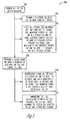
- Figure 5 shows one example of a method 500 for forming an LED panel assembly such as the LED display module 100 shown in Figure 1 .
- the description of the method 500 reference is made to elements previously described above shown in the figures. Elements and features referred to in the description of the method 500 are not intended to be exclusive but are intended to include any of the examples described in the specification and their equivalents.
- an LED seal louver such as LED seal louver 202 shown in Figures 2A and 2B is formed.
- the LED seal louver 202 includes a substrate 204 and the substrate 204 is formed with one or more substrate cavities 300 ( Figure 3 ).
- a pliable seal membrane 206 is coupled with the substrate 204. Pliable seal membrane 206 extends at least partially across the one or more substrate cavities 300 and one or more LED passages 302 extend through the pliable seal membrane 206. As previously described, in one example the one or more LED passages 302 are aligned with the substrate cavities 300.
- each substrate cavity 300 includes one or more LED passages 302. That is to say, one or more LED passages 302 extend through the pliable seal membrane 206 and are collectively aligned with one larger substrate cavity 300. The LED passages 302, in this example, are thereby fit within a single substrate cavity 300. As described above, the pliable material of the pliable seal membrane 206 continues to seal around each LED bulb 304 within each LED passage 302 where the substrate cavities 300 include a plurality of LED passages 302.
- the method 500 further includes engaging a circuit board 200 including a plurality of light emitting elements 106, such as LEDs with the LED seal louver 202.
- Engaging the circuit board with the LED seal louver includes, in one example, at 510 interference fitting one or more light emitting elements 106 within the one or more LED passages 302 where one light emitting element 106 is interference fit within each LED passage 302.
- the pliable material of the pliable seal membrane 206 extends around and engages with a single light emitting element 106 in each LED passage 302.
- the light emitting elements 106 are each coupled with the LED seal louver 202 at an interference fit 414.
- Each of the plurality of light emitting elements 106 are sealed by the pliable seal membrane 206 thereby substantially isolating the circuit board 200 from an exterior environment 410 ( Figure 4B ). While the circuit board 200 is isolated from the exterior environment each 410 of the light emitting elements 106 are project through the LED seal louver 202 including the substrate 204 and the pliable seal membrane 206. Each of the light emitting elements 106 are thereby directly visible on the display surface 102 shown in Figure 1 while the underlying circuit board is isolated from the exterior environment.
- engaging the circuit board with the LED seal louver 202 as described at 508 includes at 512, immobilizing the light emitting elements 106 interference fit within the LED passages 302.
- the LED seal louver 202 is thereby able to retain the light emitting elements 106 in a specified pattern and a specified posture.
- the specified posture includes the orientation of the light emitting elements 106 as they extend away from the circuit board 200.
- the LED seal louver 202 thereby forms an LED support skeleton, such as the support skeleton 412 shown in Figure 4 .
- the LED seal louver 202 is supported in the LED display module 100, for instance, through coupling of positioning pins 210 with pin sockets 312 on the frame 212. Fixing the LED seal louver 202 to the frame 212 ensures that the light emitting elements 106 interference fit within each of the LED passages 302 are correspondingly fixed in the specified pattern and specified posture as arranged on the circuit board 200. Time intensive and labor intensive manufacturing steps are thereby avoided because each of the light emitting elements 106 are retained in the specified pattern and the specified posture through the LED support skeleton 412 including the LED seal louver 202 cooperating with the positioning pins 210.
- coupling the pliable seal membrane 206 with the substrate 204 includes overmolding the pliable seal membrane onto the substrate.
- coupling the pliable seal membrane with the substrate includes bonding the pliable seal membrane with the substrate, including but not limited to, welding, adhering, mechanically interfitting and the like.
- engaging the circuit board 200 including the plurality of the light emitting elements 106 with the LED seal louver 202 includes forming an air gap, such as air gap 400 ( Figure 4 ), between the LED seal louver and the circuit board. The air gap extends across the circuit board 200. In another example, the air gap 400 extends across the entire circuit board 200.
- the method 500 includes coupling an edge seal, such as display edge seal 104, around the circuit board 200 and the LED seal louver 202.
- the display edge seal 104 extends from a circuit board edge 214 to an LED seal louver edge 216.
- the method 500 further includes isolating the circuit board 200 from an exterior environment 410 by way of the interference fit 414 of the light emitting elements 106 and the coupling of the display edge seal 104.
- the LED display module including the LED seal louver having a substrate and a pliable seal membrane seals the LED display module allowing each of the light emitting elements to protrude through the LED seal louver for direct viewing on the LED display surface.
- the light emitting elements project through the LED seal louver, and the pliable material in the LED seal louver extends around and interference fits with each light emitting element to substantially isolate the underlying circuit board from the environment exterior to the LED display module. Provision of the LED seal louver substantially eliminates the need for supplemental sealing techniques including potting or coating of the circuit board surface and the light emitting elements extending therefrom.
- the LED display module including the LED seal louver is thereby lighter than previous LED display modules having a potting or coating surface for sealing the light emitting element and the circuit board from the exterior environment.
- provision of the LED seal louver eliminates additional manufacturing steps including pouring of potting material, curing of the potting material, and subsequent testing of the LED display module to ensure proper alignment of each of the light emitting elements relative to the other light emitting elements on the circuit board. Stated another way, bending and misaligning of light emitting elements is avoided because the light emitting elements are not engaged with potting material poured around the light emitting elements during manufacture. Tedious and time consuming labor whether during manufacture or at a delivery site to realign the light emitting elements to provide a consistent LED display surface is thereby substantially avoided. Similarly, the provision of the LED seal louver eliminates manufacturing steps needed to apply coatings including ultraviolet and parylene coatings.
- the LED seal louver cooperates with the remainder of the LED display module to provide an LED support skeleton sized and shaped to engage with each of the light emitting elements extending through LED passages of the LED seal louver.
- the pliable seal membrane engages around each of the light emitting elements and substantially ensures the light emitting elements are maintained in the specified pattern and specified posture as they are arranged on the circuit board.
- the LED seal louver is aligned with the LED display module (including the circuit board having the light emitting elements) by positioning pins that are engaged with corresponding pin sockets. This alignment of the LED seal louver fixes the LED seal louver in place and provides the support skeleton for engagement with the light emitting elements.
- the LED seal louver cooperates with, the positioning pins for example, to substantially immobilize the light emitting elements and prevent misalignment of the light emitting elements thereby maintaining the desired appearance and display characteristics of the LED display surface.
- the air gap formed between the LED seal louver spaced from the circuit board provides insulation for the circuit board from cyclical temperature fluctuations due, for example, to seasonal changes, weather changes, temperature changes and the like.
- the circuit board is thereby exposed to substantially less dynamic heat loading providing a greater operating life for the circuit board and correspondingly decreasing field maintenance.
Landscapes
- Engineering & Computer Science (AREA)
- Physics & Mathematics (AREA)
- General Physics & Mathematics (AREA)
- Theoretical Computer Science (AREA)
- Multimedia (AREA)
- General Engineering & Computer Science (AREA)
- Led Device Packages (AREA)
- Devices For Indicating Variable Information By Combining Individual Elements (AREA)
- Fastening Of Light Sources Or Lamp Holders (AREA)
Claims (15)
- LED-Tafelanordnung (100) mit:einer Leiterplatte (200), die eine Mehrzahl von LEDs (106) umfasst;einer LED-Dichtabdeckung (202), die über die Leiterplatte gekoppelt ist, wobei die LED-Dichtabdeckung umfasst:ein Substrat (204), das einen oder mehrere Substrathohlräume (300) umfasst, wobei ein jeder des einen oder der mehreren Substrathohlräume so bemessen und geformt ist, um lose eine LED aufzunehmen,eine biegsame Dichtungsmembran (206), die mit dem Substrat gekoppelt ist, wobei die biegsame Dichtungsmembran ein biegsames Material umfasst, das sich teilweise über den einen oder die mehreren Substrathohlräume erstreckt, wobei ein oder mehrere LED-Kanäle (302) sich durch das biegsame Material benachbart zu den Substrathohlräume erstrecken, wobei ein jeder der LED-Kanäle so bemessen und geformt ist, dass er eine einzelne LED aufnimmt, undwobei Birnen (304) für eine oder mehrere der Mehrzahl von LEDs entsprechend in den LED-Kanälen aufgenommen sind, und das biegsame Material um eine jede Birne mit einem Passungssitz abdichtet; undwobei die Birnen für eine oder mehrere der Mehrzahl von LEDs durch die LED-Dichtabdeckung hindurch sichtbar sind, während die biegsame Dichtungsmembran um die Birnen abdichtet, und wobei die LED-Dichtabdeckung die Leiterplatte gegen eine äußere Umgebung der LED-Tafelanordnung abdichtet.
- LED-Tafelanordnung nach Anspruch 1, wobei die LED-Dichtabdeckung (202) mit der um die Birnen abdichtenden, biegsamen Dichtungsmembran (206) die Leiterplatte gegen eine äußere Umgebung der LED-Tafelanordnung abdichtet und isoliert.
- LED-Tafelanordnung nach Anspruch 1 oder 2, wobei die Mehrzahl der LEDs (106) in Feldern (314) auf der Leiterplatte positioniert sind und die LED-Kanäle in entsprechenden Feldern angeordnet sind.
- LED-Tafelanordnung nach Anspruch 3, wobei die Mehrzahl der LEDs (106) in Feldern positioniert sind, die eine rote, grüne und blaue LED in einem jeden Feld umfassen.
- LED-Tafelanordnung nach einem der Ansprüche 1 bis 4, wobei die LED-Kanäle (302) zwischen Abdeckungsflügeln (208) positioniert sind, die sich von einer äußeren Substratoberfläche aus erstrecken, und sich die Abdeckungsflügel wenigstens teilweise über und unter eine jede LED erstrecken, die in einem jeden LED-Kanal aufgenommen ist.
- LED-Tafelanordnung nach einem der Ansprüche 1 bis 5, wobei die LED-Dichtabdeckung von der Leiterplatte mit einem Luftspalt (400) dazwischen beabstandet ist.
- LED-Tafelanordnung nach einem der Ansprüche 1 bis 6, wobei eine oder mehrere LEDs in dem LED-Kanal mit einer LED pro Kanal aufgenommen sind, wobei die biegsame Dichtungsmembran (206) um den Birnenumfang einer jeden LED (304), aufgenommen in dem LED-Kanal, in Eingriff ist und die LEDs immobilisiert, die darin in einem speziellen Muster in einer speziellen Stellung aufgenommen sind.
- LED-Tafelanordnung nach Anspruch 7 mit einem LED-Stützgerüst (412), das umfasst:einen oder mehrere Positionierzapfen (210), die zwischen der LED-Dichtabdeckung und dem Schaltkreis gekoppelt sind,die LED-Dichtabdeckung (202), undwobei die LED-Dichtabdeckung in Eingriff steht mit einer jeden der Mehrzahl von LEDs, die in der LED-Dichtabdeckung aufgenommen sind, und wobei der eine oder die mehreren Positionierzapfen die LED-Dichtabdeckung stützen, während die LED-Dichtabdeckung eine jede der Mehrzahl von LEDs, die darin aufgenommen sind, stützt, um eine Mehrzahl von LEDs, die in den LED-Kanälen aufgenommen sind, in dem speziellen Muster und der speziellen Stellung zu halten.
- LED-Tafelanordnung nach einem der Ansprüche 1 bis 8, wobei die biegsame Dichtungsmembran (206) biegsamer ist als das Substrat.
- LED-Tafelanordnung nach einem der Ansprüche 1 bis 9, wobei die biegsame Dichtungsmembran (206) sich auf der Innenseite der LED-Dichtabdeckung befindet.
- Verfahren zum Herstellen einer LED-Tafelanordnung (100) nach Anspruch 1, welches aufweist:Bilden einer LED-Dichtabdeckung (202) umfassend:Bilden eines Substrats (204), das einen oder mehrere Substrathohlräume (300) aufweist undKoppeln einer biegsamen Dichtungsmembran (206) mit dem Substrat, wobei die biegsame Dichtungsmembran sich wenigstens teilweise über den einen oder die mehreren Substrathohlräume erstreckt, und wobei eine oder mehrere LED-Kanäle (302) sich durch die biegsame Dichtungsmembran bei den Substrathohlräumen erstrecken, wobei der eine oder die mehreren LED-Kanäle sich in einem spezifischen Muster befinden; in Eingriff stehen mit einer Leiterplatte (200) umfassend eine Mehrzahl von LEDs (106), wobei die LED-Dichtabdeckung umfasst: Passsetzen von einer oder mehreren LEDs innerhalb des einen oder der mehreren LED-Kanäle, wobei eine LED mit Presssitz sich in einem jeden LED-Kanal einfindet, und die biegsame Dichtungsmembran eine Dichtung um die Birne (304) einer jeden Presssitz-LED bildet, undFestlegen der LEDs-Presssitze in den LED-Kanälen, wobei die LED-Dichtabdeckung die LEDs in dem speziellen Muster in einer speziellen Stellung hält.
- Verfahren zur Herstellung der LED-Tafelanordnung von Anspruch 11, wobei das Koppeln der biegsamen Dichtungsmembran (206) mit dem Substrat das Überformen der biegsamen Dichtungsmembran auf dem Substrat umfasst.
- Verfahren zur Herstellung der LED-Tafelanordnung nach Anspruch 11 oder 12, wobei das Immobilisieren der LEDs-Presssitze in den LED-Kanälen das Bilden eines LED-Stützgerüsts (412) mit einem oder mehreren Positionierzapfen (210) umfasst, gekoppelt zwischen der LED-Dichtabdeckung (202) und der Leiterplatte und der LED-Dichtabdeckung, wobei der eine oder die mehreren Positionierzapfen und die LED-Dichtabdeckung zusammenwirken, um die Mehrzahl der Presssitz-LEDs in dem spezifischen Muster in der spezifischen Stellung zu halten.
- Verfahren zur Herstellung der LED-Tafelanordnung nach einem der Ansprüche 11 bis 13, das das Koppeln einer Randdichtung 104 um die Leiterplatte und die LED-Dichtabdeckung (202) aufweist, wobei sich die Randdichtung von einem Leiterplattenrand (214) zu einem LED-Dichtabdeckungsrand (216) erstreckt.
- Verfahren zum Herstellen der LED-Tafelanordnung nach Anspruch 14, die das Isolieren der Leiterplatte von der Außenumgebung mit dem Presssetzen der LEDs und der Kopplung der Randdichtung aufweist.
Applications Claiming Priority (2)
| Application Number | Priority Date | Filing Date | Title |
|---|---|---|---|
| US23673809P | 2009-08-25 | 2009-08-25 | |
| US12/859,833 US8414149B2 (en) | 2009-08-25 | 2010-08-20 | Light element seal module and method for same |
Publications (3)
| Publication Number | Publication Date |
|---|---|
| EP2290640A2 EP2290640A2 (de) | 2011-03-02 |
| EP2290640A3 EP2290640A3 (de) | 2011-03-30 |
| EP2290640B1 true EP2290640B1 (de) | 2012-08-22 |
Family
ID=43332317
Family Applications (1)
| Application Number | Title | Priority Date | Filing Date |
|---|---|---|---|
| EP10173811A Not-in-force EP2290640B1 (de) | 2009-08-25 | 2010-08-24 | Lichtelementdichtmodul und Verfahren dafür |
Country Status (2)
| Country | Link |
|---|---|
| US (2) | US8414149B2 (de) |
| EP (1) | EP2290640B1 (de) |
Families Citing this family (30)
| Publication number | Priority date | Publication date | Assignee | Title |
|---|---|---|---|---|
| US8414149B2 (en) | 2009-08-25 | 2013-04-09 | Daktronics, Inc. | Light element seal module and method for same |
| KR101641860B1 (ko) * | 2010-05-12 | 2016-07-29 | 엘지이노텍 주식회사 | 발광소자 어레이, 조명장치 및 백라이트 장치 |
| US10078975B2 (en) | 2010-09-22 | 2018-09-18 | Skyline Products, Inc. | Highway variable message sign with apertures |
| US9343000B2 (en) * | 2010-09-22 | 2016-05-17 | Skyline Products, Inc. | Fine pitch full color variable message sign |
| CN104584105B (zh) | 2012-06-28 | 2017-11-17 | 达科电子股份有限公司 | 显示模块 |
| CN104584106B (zh) | 2012-06-28 | 2017-09-12 | 达科电子股份有限公司 | 显示模块的安装 |
| US8974077B2 (en) | 2012-07-30 | 2015-03-10 | Ultravision Technologies, Llc | Heat sink for LED light source |
| US20140153241A1 (en) * | 2012-12-01 | 2014-06-05 | Lsi Industries, Inc. | Display board and display board components |
| US9852666B2 (en) | 2013-03-16 | 2017-12-26 | Adti Media Llc | Full height sectional sign assembly and installation kit and method of using same |
| US8929083B2 (en) | 2013-03-16 | 2015-01-06 | ADIT Media, LLC | Compound structural frame and method of using same for efficient retrofitting |
| US8824125B1 (en) | 2013-03-16 | 2014-09-02 | ADTI Media, LLC | Modular installation and conversion kit for electronic sign structure and method of using same |
| US10210778B2 (en) | 2013-03-16 | 2019-02-19 | Adti Media Llc | Sign construction with sectional sign assemblies and installation kit and method of using same |
| US9047791B2 (en) | 2013-03-16 | 2015-06-02 | Adti Media, Llc. | Sign construction with sectional sign assemblies and installation kit and method of using same |
| US9761157B2 (en) | 2013-03-16 | 2017-09-12 | Adti Media Llc | Customized sectional sign assembly kit and method of using kit for construction and installation of same |
| US9416551B2 (en) | 2013-12-31 | 2016-08-16 | Ultravision Technologies, Llc | Preassembled display systems and methods of installation thereof |
| US9207904B2 (en) | 2013-12-31 | 2015-12-08 | Ultravision Technologies, Llc | Multi-panel display with hot swappable display panels and methods of servicing thereof |
| US20150187237A1 (en) | 2013-12-31 | 2015-07-02 | Ultravision Holdings, Llc | System and Method for a Modular Multi-Panel Display |
| US9582237B2 (en) | 2013-12-31 | 2017-02-28 | Ultravision Technologies, Llc | Modular display panels with different pitches |
| US9195281B2 (en) | 2013-12-31 | 2015-11-24 | Ultravision Technologies, Llc | System and method for a modular multi-panel display |
| CN204010562U (zh) * | 2014-06-18 | 2014-12-10 | 张海龙 | 防水散热的led显示屏灯箱 |
| US10706770B2 (en) | 2014-07-16 | 2020-07-07 | Ultravision Technologies, Llc | Display system having module display panel with circuitry for bidirectional communication |
| DE102015010413A1 (de) * | 2015-08-14 | 2017-03-02 | microTec Gesellschaft für Mikrotechnologie mbH | Vorrichtung zur Beleuchtung einer Maske mit einem Hochleistungs-LED-Array |
| WO2017136410A1 (en) * | 2016-02-02 | 2017-08-10 | Metromedia Technologies, Inc. | Led billboard system |
| EP3205584B1 (de) | 2016-02-12 | 2020-06-03 | Goodrich Lighting Systems GmbH | Äussere flugzeugbeleuchtung und flugzeug damit |
| USD804712S1 (en) * | 2016-05-23 | 2017-12-05 | Roe Visual Co., Ltd. | LED display screen with a quick installation structure |
| US20180084217A1 (en) * | 2016-09-20 | 2018-03-22 | Aeson LED Display Technologies, Inc. | Led video cabinet having a native 16:9 aspect ratio |
| CN109147590A (zh) * | 2018-11-16 | 2019-01-04 | 深圳市光祥科技股份有限公司 | Led显示屏 |
| US11333342B2 (en) * | 2019-05-29 | 2022-05-17 | Nbcuniversal Media, Llc | Light emitting diode cooling systems and methods |
| CN115440142B (zh) * | 2022-08-22 | 2024-12-27 | 深圳市美亚迪光电有限公司 | 一种led显示屏软模组的制作方法及软模组 |
| US12025302B1 (en) | 2023-04-28 | 2024-07-02 | NBCUniversal Studios LLC | Light emitting diode lighting systems and methods |
Family Cites Families (5)
| Publication number | Priority date | Publication date | Assignee | Title |
|---|---|---|---|---|
| US5914698A (en) | 1996-04-15 | 1999-06-22 | Addco Manufacturing, Inc. | Modular message board |
| JP2001249629A (ja) | 2000-03-08 | 2001-09-14 | Matsushita Electric Ind Co Ltd | Led表示エレメント |
| US20020122134A1 (en) | 2001-03-05 | 2002-09-05 | Kalua Kevin A. | Video display array of sealed, modular units |
| CN201233693Y (zh) * | 2008-06-20 | 2009-05-06 | 深圳市联腾科技有限公司 | Led显示模组 |
| US8414149B2 (en) | 2009-08-25 | 2013-04-09 | Daktronics, Inc. | Light element seal module and method for same |
-
2010
- 2010-08-20 US US12/859,833 patent/US8414149B2/en active Active
- 2010-08-24 EP EP10173811A patent/EP2290640B1/de not_active Not-in-force
-
2013
- 2013-04-08 US US13/858,508 patent/US8721116B2/en active Active
Also Published As
| Publication number | Publication date |
|---|---|
| US20130229797A1 (en) | 2013-09-05 |
| US8721116B2 (en) | 2014-05-13 |
| US20110051409A1 (en) | 2011-03-03 |
| US8414149B2 (en) | 2013-04-09 |
| EP2290640A2 (de) | 2011-03-02 |
| EP2290640A3 (de) | 2011-03-30 |
Similar Documents
| Publication | Publication Date | Title |
|---|---|---|
| EP2290640B1 (de) | Lichtelementdichtmodul und Verfahren dafür | |
| EP3179468B1 (de) | Verkapselung von lichtemittierenden elementen auf einem anzeigemodul | |
| US8111208B2 (en) | Front and rear removable panel for electronic displays | |
| CN100533515C (zh) | 模块化显示系统 | |
| US9557954B2 (en) | Display panel using direct emission pixel arrays | |
| US6538709B1 (en) | LCD panel including plurality of display panel parts wrapped around by a thin plastic film envelope with an opening | |
| US9696573B2 (en) | Display module and liquid crystal display device including the same | |
| JP6548733B2 (ja) | 表示ユニット及び表示ユニットの製造方法 | |
| US20160225295A1 (en) | Frame panel for three-dimensional sign board, three-dimensional sign board comprising same, and manufacturing method therefor | |
| US20230284389A1 (en) | Light Module With Discrete Optics and Methods of Assembling Same | |
| CN115087832A (zh) | 加固型dv-led显示系统和模块,以及制造dv-led显示器的方法 | |
| KR100682073B1 (ko) | 디스플레이장치용 led모듈 박스어셈블리 | |
| KR20110133737A (ko) | 박막 필름 커버를 구비한 엘이디 표시장치 | |
| KR100892368B1 (ko) | 액정표시장치 및 그의 제조방법 | |
| KR100950972B1 (ko) | 발광 다이오드 전광판 | |
| JPH05323881A (ja) | 多色表示装置 | |
| HK40079686A (en) | Ruggedized dv-led display systems and modules, and methods of manufacturing dv-led displays | |
| KR20190047987A (ko) | 디스플레이 장치 | |
| HK40011708A (en) | Display unit, display device and method for manufacturing display unit | |
| HK40011708B (en) | Display unit, display device and method for manufacturing display unit | |
| JPH0485584A (ja) | 表示素子装置 |
Legal Events
| Date | Code | Title | Description |
|---|---|---|---|
| PUAI | Public reference made under article 153(3) epc to a published international application that has entered the european phase |
Free format text: ORIGINAL CODE: 0009012 |
|
| PUAL | Search report despatched |
Free format text: ORIGINAL CODE: 0009013 |
|
| AK | Designated contracting states |
Kind code of ref document: A2 Designated state(s): AL AT BE BG CH CY CZ DE DK EE ES FI FR GB GR HR HU IE IS IT LI LT LU LV MC MK MT NL NO PL PT RO SE SI SK SM TR |
|
| AX | Request for extension of the european patent |
Extension state: BA ME RS |
|
| AK | Designated contracting states |
Kind code of ref document: A3 Designated state(s): AL AT BE BG CH CY CZ DE DK EE ES FI FR GB GR HR HU IE IS IT LI LT LU LV MC MK MT NL NO PL PT RO SE SI SK SM TR |
|
| AX | Request for extension of the european patent |
Extension state: BA ME RS |
|
| 17P | Request for examination filed |
Effective date: 20110922 |
|
| GRAP | Despatch of communication of intention to grant a patent |
Free format text: ORIGINAL CODE: EPIDOSNIGR1 |
|
| GRAS | Grant fee paid |
Free format text: ORIGINAL CODE: EPIDOSNIGR3 |
|
| GRAA | (expected) grant |
Free format text: ORIGINAL CODE: 0009210 |
|
| AK | Designated contracting states |
Kind code of ref document: B1 Designated state(s): AL AT BE BG CH CY CZ DE DK EE ES FI FR GB GR HR HU IE IS IT LI LT LU LV MC MK MT NL NO PL PT RO SE SI SK SM TR |
|
| REG | Reference to a national code |
Ref country code: GB Ref legal event code: FG4D |
|
| REG | Reference to a national code |
Ref country code: CH Ref legal event code: EP |
|
| REG | Reference to a national code |
Ref country code: IE Ref legal event code: FG4D |
|
| REG | Reference to a national code |
Ref country code: AT Ref legal event code: REF Ref document number: 572320 Country of ref document: AT Kind code of ref document: T Effective date: 20120915 |
|
| REG | Reference to a national code |
Ref country code: DE Ref legal event code: R096 Ref document number: 602010002429 Country of ref document: DE Effective date: 20121018 |
|
| REG | Reference to a national code |
Ref country code: NL Ref legal event code: VDEP Effective date: 20120822 |
|
| REG | Reference to a national code |
Ref country code: AT Ref legal event code: MK05 Ref document number: 572320 Country of ref document: AT Kind code of ref document: T Effective date: 20120822 |
|
| REG | Reference to a national code |
Ref country code: LT Ref legal event code: MG4D Effective date: 20120822 |
|
| PG25 | Lapsed in a contracting state [announced via postgrant information from national office to epo] |
Ref country code: LT Free format text: LAPSE BECAUSE OF FAILURE TO SUBMIT A TRANSLATION OF THE DESCRIPTION OR TO PAY THE FEE WITHIN THE PRESCRIBED TIME-LIMIT Effective date: 20120822 Ref country code: AT Free format text: LAPSE BECAUSE OF FAILURE TO SUBMIT A TRANSLATION OF THE DESCRIPTION OR TO PAY THE FEE WITHIN THE PRESCRIBED TIME-LIMIT Effective date: 20120822 Ref country code: IS Free format text: LAPSE BECAUSE OF FAILURE TO SUBMIT A TRANSLATION OF THE DESCRIPTION OR TO PAY THE FEE WITHIN THE PRESCRIBED TIME-LIMIT Effective date: 20121222 Ref country code: FI Free format text: LAPSE BECAUSE OF FAILURE TO SUBMIT A TRANSLATION OF THE DESCRIPTION OR TO PAY THE FEE WITHIN THE PRESCRIBED TIME-LIMIT Effective date: 20120822 Ref country code: NO Free format text: LAPSE BECAUSE OF FAILURE TO SUBMIT A TRANSLATION OF THE DESCRIPTION OR TO PAY THE FEE WITHIN THE PRESCRIBED TIME-LIMIT Effective date: 20121122 Ref country code: HR Free format text: LAPSE BECAUSE OF FAILURE TO SUBMIT A TRANSLATION OF THE DESCRIPTION OR TO PAY THE FEE WITHIN THE PRESCRIBED TIME-LIMIT Effective date: 20120822 |
|
| PG25 | Lapsed in a contracting state [announced via postgrant information from national office to epo] |
Ref country code: GR Free format text: LAPSE BECAUSE OF FAILURE TO SUBMIT A TRANSLATION OF THE DESCRIPTION OR TO PAY THE FEE WITHIN THE PRESCRIBED TIME-LIMIT Effective date: 20121123 Ref country code: PT Free format text: LAPSE BECAUSE OF FAILURE TO SUBMIT A TRANSLATION OF THE DESCRIPTION OR TO PAY THE FEE WITHIN THE PRESCRIBED TIME-LIMIT Effective date: 20121224 Ref country code: SI Free format text: LAPSE BECAUSE OF FAILURE TO SUBMIT A TRANSLATION OF THE DESCRIPTION OR TO PAY THE FEE WITHIN THE PRESCRIBED TIME-LIMIT Effective date: 20120822 Ref country code: BE Free format text: LAPSE BECAUSE OF FAILURE TO SUBMIT A TRANSLATION OF THE DESCRIPTION OR TO PAY THE FEE WITHIN THE PRESCRIBED TIME-LIMIT Effective date: 20120822 Ref country code: LV Free format text: LAPSE BECAUSE OF FAILURE TO SUBMIT A TRANSLATION OF THE DESCRIPTION OR TO PAY THE FEE WITHIN THE PRESCRIBED TIME-LIMIT Effective date: 20120822 Ref country code: SE Free format text: LAPSE BECAUSE OF FAILURE TO SUBMIT A TRANSLATION OF THE DESCRIPTION OR TO PAY THE FEE WITHIN THE PRESCRIBED TIME-LIMIT Effective date: 20120822 |
|
| PG25 | Lapsed in a contracting state [announced via postgrant information from national office to epo] |
Ref country code: MC Free format text: LAPSE BECAUSE OF NON-PAYMENT OF DUE FEES Effective date: 20120831 Ref country code: NL Free format text: LAPSE BECAUSE OF FAILURE TO SUBMIT A TRANSLATION OF THE DESCRIPTION OR TO PAY THE FEE WITHIN THE PRESCRIBED TIME-LIMIT Effective date: 20120822 |
|
| PG25 | Lapsed in a contracting state [announced via postgrant information from national office to epo] |
Ref country code: DK Free format text: LAPSE BECAUSE OF FAILURE TO SUBMIT A TRANSLATION OF THE DESCRIPTION OR TO PAY THE FEE WITHIN THE PRESCRIBED TIME-LIMIT Effective date: 20120822 Ref country code: RO Free format text: LAPSE BECAUSE OF FAILURE TO SUBMIT A TRANSLATION OF THE DESCRIPTION OR TO PAY THE FEE WITHIN THE PRESCRIBED TIME-LIMIT Effective date: 20120822 Ref country code: ES Free format text: LAPSE BECAUSE OF FAILURE TO SUBMIT A TRANSLATION OF THE DESCRIPTION OR TO PAY THE FEE WITHIN THE PRESCRIBED TIME-LIMIT Effective date: 20121203 Ref country code: EE Free format text: LAPSE BECAUSE OF FAILURE TO SUBMIT A TRANSLATION OF THE DESCRIPTION OR TO PAY THE FEE WITHIN THE PRESCRIBED TIME-LIMIT Effective date: 20120822 Ref country code: CZ Free format text: LAPSE BECAUSE OF FAILURE TO SUBMIT A TRANSLATION OF THE DESCRIPTION OR TO PAY THE FEE WITHIN THE PRESCRIBED TIME-LIMIT Effective date: 20120822 |
|
| REG | Reference to a national code |
Ref country code: IE Ref legal event code: MM4A |
|
| PG25 | Lapsed in a contracting state [announced via postgrant information from national office to epo] |
Ref country code: SK Free format text: LAPSE BECAUSE OF FAILURE TO SUBMIT A TRANSLATION OF THE DESCRIPTION OR TO PAY THE FEE WITHIN THE PRESCRIBED TIME-LIMIT Effective date: 20120822 Ref country code: PL Free format text: LAPSE BECAUSE OF FAILURE TO SUBMIT A TRANSLATION OF THE DESCRIPTION OR TO PAY THE FEE WITHIN THE PRESCRIBED TIME-LIMIT Effective date: 20120822 Ref country code: IT Free format text: LAPSE BECAUSE OF FAILURE TO SUBMIT A TRANSLATION OF THE DESCRIPTION OR TO PAY THE FEE WITHIN THE PRESCRIBED TIME-LIMIT Effective date: 20120822 |
|
| PLBE | No opposition filed within time limit |
Free format text: ORIGINAL CODE: 0009261 |
|
| STAA | Information on the status of an ep patent application or granted ep patent |
Free format text: STATUS: NO OPPOSITION FILED WITHIN TIME LIMIT |
|
| 26N | No opposition filed |
Effective date: 20130523 |
|
| PG25 | Lapsed in a contracting state [announced via postgrant information from national office to epo] |
Ref country code: BG Free format text: LAPSE BECAUSE OF FAILURE TO SUBMIT A TRANSLATION OF THE DESCRIPTION OR TO PAY THE FEE WITHIN THE PRESCRIBED TIME-LIMIT Effective date: 20121122 Ref country code: IE Free format text: LAPSE BECAUSE OF NON-PAYMENT OF DUE FEES Effective date: 20120824 |
|
| REG | Reference to a national code |
Ref country code: DE Ref legal event code: R097 Ref document number: 602010002429 Country of ref document: DE Effective date: 20130523 |
|
| PG25 | Lapsed in a contracting state [announced via postgrant information from national office to epo] |
Ref country code: CY Free format text: LAPSE BECAUSE OF FAILURE TO SUBMIT A TRANSLATION OF THE DESCRIPTION OR TO PAY THE FEE WITHIN THE PRESCRIBED TIME-LIMIT Effective date: 20120822 Ref country code: AL Free format text: LAPSE BECAUSE OF FAILURE TO SUBMIT A TRANSLATION OF THE DESCRIPTION OR TO PAY THE FEE WITHIN THE PRESCRIBED TIME-LIMIT Effective date: 20120822 Ref country code: MT Free format text: LAPSE BECAUSE OF FAILURE TO SUBMIT A TRANSLATION OF THE DESCRIPTION OR TO PAY THE FEE WITHIN THE PRESCRIBED TIME-LIMIT Effective date: 20120822 |
|
| PG25 | Lapsed in a contracting state [announced via postgrant information from national office to epo] |
Ref country code: TR Free format text: LAPSE BECAUSE OF FAILURE TO SUBMIT A TRANSLATION OF THE DESCRIPTION OR TO PAY THE FEE WITHIN THE PRESCRIBED TIME-LIMIT Effective date: 20120822 |
|
| PG25 | Lapsed in a contracting state [announced via postgrant information from national office to epo] |
Ref country code: SM Free format text: LAPSE BECAUSE OF FAILURE TO SUBMIT A TRANSLATION OF THE DESCRIPTION OR TO PAY THE FEE WITHIN THE PRESCRIBED TIME-LIMIT Effective date: 20120822 Ref country code: LU Free format text: LAPSE BECAUSE OF NON-PAYMENT OF DUE FEES Effective date: 20120824 |
|
| PG25 | Lapsed in a contracting state [announced via postgrant information from national office to epo] |
Ref country code: HU Free format text: LAPSE BECAUSE OF FAILURE TO SUBMIT A TRANSLATION OF THE DESCRIPTION OR TO PAY THE FEE WITHIN THE PRESCRIBED TIME-LIMIT Effective date: 20100824 |
|
| REG | Reference to a national code |
Ref country code: CH Ref legal event code: PL |
|
| PG25 | Lapsed in a contracting state [announced via postgrant information from national office to epo] |
Ref country code: CH Free format text: LAPSE BECAUSE OF NON-PAYMENT OF DUE FEES Effective date: 20140831 Ref country code: LI Free format text: LAPSE BECAUSE OF NON-PAYMENT OF DUE FEES Effective date: 20140831 |
|
| PG25 | Lapsed in a contracting state [announced via postgrant information from national office to epo] |
Ref country code: MK Free format text: LAPSE BECAUSE OF FAILURE TO SUBMIT A TRANSLATION OF THE DESCRIPTION OR TO PAY THE FEE WITHIN THE PRESCRIBED TIME-LIMIT Effective date: 20120822 |
|
| REG | Reference to a national code |
Ref country code: FR Ref legal event code: PLFP Year of fee payment: 6 |
|
| REG | Reference to a national code |
Ref country code: FR Ref legal event code: PLFP Year of fee payment: 7 |
|
| REG | Reference to a national code |
Ref country code: FR Ref legal event code: PLFP Year of fee payment: 8 |
|
| REG | Reference to a national code |
Ref country code: FR Ref legal event code: PLFP Year of fee payment: 9 |
|
| PGFP | Annual fee paid to national office [announced via postgrant information from national office to epo] |
Ref country code: FR Payment date: 20180827 Year of fee payment: 9 Ref country code: DE Payment date: 20180829 Year of fee payment: 9 |
|
| PGFP | Annual fee paid to national office [announced via postgrant information from national office to epo] |
Ref country code: GB Payment date: 20180828 Year of fee payment: 9 |
|
| REG | Reference to a national code |
Ref country code: DE Ref legal event code: R119 Ref document number: 602010002429 Country of ref document: DE |
|
| GBPC | Gb: european patent ceased through non-payment of renewal fee |
Effective date: 20190824 |
|
| PG25 | Lapsed in a contracting state [announced via postgrant information from national office to epo] |
Ref country code: DE Free format text: LAPSE BECAUSE OF NON-PAYMENT OF DUE FEES Effective date: 20200303 Ref country code: FR Free format text: LAPSE BECAUSE OF NON-PAYMENT OF DUE FEES Effective date: 20190831 |
|
| PG25 | Lapsed in a contracting state [announced via postgrant information from national office to epo] |
Ref country code: GB Free format text: LAPSE BECAUSE OF NON-PAYMENT OF DUE FEES Effective date: 20190824 |