EP2289983B1 - Composite film - Google Patents
Composite film Download PDFInfo
- Publication number
- EP2289983B1 EP2289983B1 EP20100174842 EP10174842A EP2289983B1 EP 2289983 B1 EP2289983 B1 EP 2289983B1 EP 20100174842 EP20100174842 EP 20100174842 EP 10174842 A EP10174842 A EP 10174842A EP 2289983 B1 EP2289983 B1 EP 2289983B1
- Authority
- EP
- European Patent Office
- Prior art keywords
- layer
- gas barrier
- film
- composite film
- adhesive
- Prior art date
- Legal status (The legal status is an assumption and is not a legal conclusion. Google has not performed a legal analysis and makes no representation as to the accuracy of the status listed.)
- Not-in-force
Links
- 239000002131 composite material Substances 0.000 title claims abstract description 68
- 239000010410 layer Substances 0.000 claims abstract description 97
- 230000004888 barrier function Effects 0.000 claims abstract description 85
- 239000012044 organic layer Substances 0.000 claims abstract description 61
- 239000012790 adhesive layer Substances 0.000 claims abstract description 41
- 239000000853 adhesive Substances 0.000 claims abstract description 34
- 229910052751 metal Inorganic materials 0.000 claims abstract description 33
- 239000002184 metal Substances 0.000 claims abstract description 33
- 230000001070 adhesive effect Effects 0.000 claims abstract description 32
- 239000000758 substrate Substances 0.000 claims abstract description 29
- 150000004703 alkoxides Chemical class 0.000 claims abstract description 25
- 238000009820 dry lamination Methods 0.000 claims abstract description 15
- 238000000034 method Methods 0.000 claims description 37
- 150000001875 compounds Chemical class 0.000 claims description 22
- 239000000203 mixture Substances 0.000 claims description 19
- 239000006087 Silane Coupling Agent Substances 0.000 claims description 16
- 229920005989 resin Polymers 0.000 claims description 14
- 239000011347 resin Substances 0.000 claims description 14
- 238000010030 laminating Methods 0.000 claims description 11
- VYPSYNLAJGMNEJ-UHFFFAOYSA-N Silicium dioxide Chemical compound O=[Si]=O VYPSYNLAJGMNEJ-UHFFFAOYSA-N 0.000 claims description 9
- 229910052814 silicon oxide Inorganic materials 0.000 claims description 9
- 239000004814 polyurethane Substances 0.000 claims description 7
- 229920002635 polyurethane Polymers 0.000 claims description 7
- NIXOWILDQLNWCW-UHFFFAOYSA-M Acrylate Chemical compound [O-]C(=O)C=C NIXOWILDQLNWCW-UHFFFAOYSA-M 0.000 claims description 6
- 229910052782 aluminium Inorganic materials 0.000 claims description 6
- XAGFODPZIPBFFR-UHFFFAOYSA-N aluminium Chemical compound [Al] XAGFODPZIPBFFR-UHFFFAOYSA-N 0.000 claims description 4
- 239000007788 liquid Substances 0.000 claims description 4
- 238000002156 mixing Methods 0.000 claims description 4
- 229920000728 polyester Polymers 0.000 claims description 4
- 238000004519 manufacturing process Methods 0.000 claims description 2
- 239000002210 silicon-based material Substances 0.000 claims description 2
- 239000010408 film Substances 0.000 description 137
- 239000007789 gas Substances 0.000 description 57
- XLYOFNOQVPJJNP-UHFFFAOYSA-N water Chemical compound O XLYOFNOQVPJJNP-UHFFFAOYSA-N 0.000 description 22
- 230000035699 permeability Effects 0.000 description 20
- 230000015572 biosynthetic process Effects 0.000 description 12
- QVGXLLKOCUKJST-UHFFFAOYSA-N atomic oxygen Chemical compound [O] QVGXLLKOCUKJST-UHFFFAOYSA-N 0.000 description 11
- 239000001301 oxygen Substances 0.000 description 11
- 229910052760 oxygen Inorganic materials 0.000 description 11
- 230000008569 process Effects 0.000 description 11
- NIHNNTQXNPWCJQ-UHFFFAOYSA-N fluorene Chemical compound C1=CC=C2CC3=CC=CC=C3C2=C1 NIHNNTQXNPWCJQ-UHFFFAOYSA-N 0.000 description 10
- -1 that is Substances 0.000 description 10
- 150000001252 acrylic acid derivatives Chemical class 0.000 description 9
- 239000004417 polycarbonate Substances 0.000 description 9
- 238000006116 polymerization reaction Methods 0.000 description 9
- 238000004544 sputter deposition Methods 0.000 description 9
- DAKWPKUUDNSNPN-UHFFFAOYSA-N Trimethylolpropane triacrylate Chemical compound C=CC(=O)OCC(CC)(COC(=O)C=C)COC(=O)C=C DAKWPKUUDNSNPN-UHFFFAOYSA-N 0.000 description 8
- 238000005452 bending Methods 0.000 description 8
- 229910052738 indium Inorganic materials 0.000 description 8
- 239000002985 plastic film Substances 0.000 description 8
- 229920006255 plastic film Polymers 0.000 description 8
- 229910052802 copper Inorganic materials 0.000 description 7
- 239000010949 copper Substances 0.000 description 7
- RYGMFSIKBFXOCR-UHFFFAOYSA-N Copper Chemical compound [Cu] RYGMFSIKBFXOCR-UHFFFAOYSA-N 0.000 description 6
- BUGBHKTXTAQXES-UHFFFAOYSA-N Selenium Chemical compound [Se] BUGBHKTXTAQXES-UHFFFAOYSA-N 0.000 description 6
- APFVFJFRJDLVQX-UHFFFAOYSA-N indium atom Chemical compound [In] APFVFJFRJDLVQX-UHFFFAOYSA-N 0.000 description 6
- 239000002346 layers by function Substances 0.000 description 6
- 229920000515 polycarbonate Polymers 0.000 description 6
- 229910052711 selenium Inorganic materials 0.000 description 6
- 239000011669 selenium Substances 0.000 description 6
- 229910052710 silicon Inorganic materials 0.000 description 6
- 0 CCC(C(C)C(CCC(CC(C)C(*C)C(C)(CCCC1)CC1[C@@](C1C2C3C1C1C3C1)C2=CC1C(C)*CC1)C1C)C1C1CCCCC1)C(CC1)CC1C(C1C(C)C1C)(C(C)*1)C2C1C(C)CC2 Chemical compound CCC(C(C)C(CCC(CC(C)C(*C)C(C)(CCCC1)CC1[C@@](C1C2C3C1C1C3C1)C2=CC1C(C)*CC1)C1C)C1C1CCCCC1)C(CC1)CC1C(C1C(C)C1C)(C(C)*1)C2C1C(C)CC2 0.000 description 5
- 238000000576 coating method Methods 0.000 description 5
- 230000000052 comparative effect Effects 0.000 description 5
- 238000000151 deposition Methods 0.000 description 5
- 230000008021 deposition Effects 0.000 description 5
- GYHNNYVSQQEPJS-UHFFFAOYSA-N Gallium Chemical compound [Ga] GYHNNYVSQQEPJS-UHFFFAOYSA-N 0.000 description 4
- PPBRXRYQALVLMV-UHFFFAOYSA-N Styrene Natural products C=CC1=CC=CC=C1 PPBRXRYQALVLMV-UHFFFAOYSA-N 0.000 description 4
- 125000002723 alicyclic group Chemical group 0.000 description 4
- 229920001577 copolymer Polymers 0.000 description 4
- 230000007547 defect Effects 0.000 description 4
- 229910052733 gallium Inorganic materials 0.000 description 4
- 239000000463 material Substances 0.000 description 4
- 150000004767 nitrides Chemical class 0.000 description 4
- 229920000620 organic polymer Polymers 0.000 description 4
- 239000002245 particle Substances 0.000 description 4
- 230000009467 reduction Effects 0.000 description 4
- 239000004065 semiconductor Substances 0.000 description 4
- 239000000126 substance Substances 0.000 description 4
- 238000002834 transmittance Methods 0.000 description 4
- IJGRMHOSHXDMSA-UHFFFAOYSA-N Atomic nitrogen Chemical compound N#N IJGRMHOSHXDMSA-UHFFFAOYSA-N 0.000 description 3
- CERQOIWHTDAKMF-UHFFFAOYSA-M Methacrylate Chemical compound CC(=C)C([O-])=O CERQOIWHTDAKMF-UHFFFAOYSA-M 0.000 description 3
- 239000004642 Polyimide Substances 0.000 description 3
- XUIMIQQOPSSXEZ-UHFFFAOYSA-N Silicon Chemical group [Si] XUIMIQQOPSSXEZ-UHFFFAOYSA-N 0.000 description 3
- 230000002708 enhancing effect Effects 0.000 description 3
- QSHDDOUJBYECFT-UHFFFAOYSA-N mercury Chemical compound [Hg] QSHDDOUJBYECFT-UHFFFAOYSA-N 0.000 description 3
- 229910052753 mercury Inorganic materials 0.000 description 3
- 239000000178 monomer Substances 0.000 description 3
- MWUXSHHQAYIFBG-UHFFFAOYSA-N nitrogen oxide Inorganic materials O=[N] MWUXSHHQAYIFBG-UHFFFAOYSA-N 0.000 description 3
- 229920002492 poly(sulfone) Polymers 0.000 description 3
- 229920001230 polyarylate Polymers 0.000 description 3
- 229920005668 polycarbonate resin Polymers 0.000 description 3
- 239000004431 polycarbonate resin Substances 0.000 description 3
- 229920001721 polyimide Polymers 0.000 description 3
- 239000003505 polymerization initiator Substances 0.000 description 3
- 229920000098 polyolefin Polymers 0.000 description 3
- 239000010409 thin film Substances 0.000 description 3
- 229910052719 titanium Inorganic materials 0.000 description 3
- QNODIIQQMGDSEF-UHFFFAOYSA-N (1-hydroxycyclohexyl)-phenylmethanone Chemical compound C=1C=CC=CC=1C(=O)C1(O)CCCCC1 QNODIIQQMGDSEF-UHFFFAOYSA-N 0.000 description 2
- ODIGIKRIUKFKHP-UHFFFAOYSA-N (n-propan-2-yloxycarbonylanilino) acetate Chemical compound CC(C)OC(=O)N(OC(C)=O)C1=CC=CC=C1 ODIGIKRIUKFKHP-UHFFFAOYSA-N 0.000 description 2
- MYRTYDVEIRVNKP-UHFFFAOYSA-N 1,2-Divinylbenzene Chemical compound C=CC1=CC=CC=C1C=C MYRTYDVEIRVNKP-UHFFFAOYSA-N 0.000 description 2
- FUGYGGDSWSUORM-UHFFFAOYSA-N 4-hydroxystyrene Chemical compound OC1=CC=C(C=C)C=C1 FUGYGGDSWSUORM-UHFFFAOYSA-N 0.000 description 2
- XKRFYHLGVUSROY-UHFFFAOYSA-N Argon Chemical compound [Ar] XKRFYHLGVUSROY-UHFFFAOYSA-N 0.000 description 2
- JBRZTFJDHDCESZ-UHFFFAOYSA-N AsGa Chemical compound [As]#[Ga] JBRZTFJDHDCESZ-UHFFFAOYSA-N 0.000 description 2
- 229920002799 BoPET Polymers 0.000 description 2
- 239000004593 Epoxy Substances 0.000 description 2
- 239000004696 Poly ether ether ketone Substances 0.000 description 2
- 239000004695 Polyether sulfone Substances 0.000 description 2
- 239000004697 Polyetherimide Substances 0.000 description 2
- NINIDFKCEFEMDL-UHFFFAOYSA-N Sulfur Chemical compound [S] NINIDFKCEFEMDL-UHFFFAOYSA-N 0.000 description 2
- 238000007611 bar coating method Methods 0.000 description 2
- RPPBZEBXAAZZJH-UHFFFAOYSA-N cadmium telluride Chemical compound [Te]=[Cd] RPPBZEBXAAZZJH-UHFFFAOYSA-N 0.000 description 2
- 239000002775 capsule Substances 0.000 description 2
- 239000001913 cellulose Substances 0.000 description 2
- 229920002678 cellulose Polymers 0.000 description 2
- 239000003795 chemical substances by application Substances 0.000 description 2
- 238000005229 chemical vapour deposition Methods 0.000 description 2
- 239000011248 coating agent Substances 0.000 description 2
- 239000004615 ingredient Substances 0.000 description 2
- 239000003999 initiator Substances 0.000 description 2
- 238000007733 ion plating Methods 0.000 description 2
- 239000002075 main ingredient Substances 0.000 description 2
- 238000005259 measurement Methods 0.000 description 2
- 150000001247 metal acetylides Chemical class 0.000 description 2
- 229910044991 metal oxide Inorganic materials 0.000 description 2
- 150000004706 metal oxides Chemical class 0.000 description 2
- 229910052757 nitrogen Inorganic materials 0.000 description 2
- 238000005240 physical vapour deposition Methods 0.000 description 2
- 238000005268 plasma chemical vapour deposition Methods 0.000 description 2
- 229920003207 poly(ethylene-2,6-naphthalate) Polymers 0.000 description 2
- 229920002312 polyamide-imide Polymers 0.000 description 2
- 229920001225 polyester resin Polymers 0.000 description 2
- 239000004645 polyester resin Substances 0.000 description 2
- 229920006393 polyether sulfone Polymers 0.000 description 2
- 229920002530 polyetherether ketone Polymers 0.000 description 2
- 229920001601 polyetherimide Polymers 0.000 description 2
- 239000011112 polyethylene naphthalate Substances 0.000 description 2
- 230000005855 radiation Effects 0.000 description 2
- 229910052717 sulfur Inorganic materials 0.000 description 2
- 239000011593 sulfur Substances 0.000 description 2
- 229920005992 thermoplastic resin Polymers 0.000 description 2
- 229910052718 tin Inorganic materials 0.000 description 2
- 239000010936 titanium Substances 0.000 description 2
- 229910052725 zinc Inorganic materials 0.000 description 2
- KWVGIHKZDCUPEU-UHFFFAOYSA-N 2,2-dimethoxy-2-phenylacetophenone Chemical compound C=1C=CC=CC=1C(OC)(OC)C(=O)C1=CC=CC=C1 KWVGIHKZDCUPEU-UHFFFAOYSA-N 0.000 description 1
- GJKGAPPUXSSCFI-UHFFFAOYSA-N 2-Hydroxy-4'-(2-hydroxyethoxy)-2-methylpropiophenone Chemical compound CC(C)(O)C(=O)C1=CC=C(OCCO)C=C1 GJKGAPPUXSSCFI-UHFFFAOYSA-N 0.000 description 1
- FIOCEWASVZHBTK-UHFFFAOYSA-N 2-[2-(2-oxo-2-phenylacetyl)oxyethoxy]ethyl 2-oxo-2-phenylacetate Chemical compound C=1C=CC=CC=1C(=O)C(=O)OCCOCCOC(=O)C(=O)C1=CC=CC=C1 FIOCEWASVZHBTK-UHFFFAOYSA-N 0.000 description 1
- UHFFVFAKEGKNAQ-UHFFFAOYSA-N 2-benzyl-2-(dimethylamino)-1-(4-morpholin-4-ylphenyl)butan-1-one Chemical compound C=1C=C(N2CCOCC2)C=CC=1C(=O)C(CC)(N(C)C)CC1=CC=CC=C1 UHFFVFAKEGKNAQ-UHFFFAOYSA-N 0.000 description 1
- XMLYCEVDHLAQEL-UHFFFAOYSA-N 2-hydroxy-2-methyl-1-phenylpropan-1-one Chemical compound CC(C)(O)C(=O)C1=CC=CC=C1 XMLYCEVDHLAQEL-UHFFFAOYSA-N 0.000 description 1
- LWRBVKNFOYUCNP-UHFFFAOYSA-N 2-methyl-1-(4-methylsulfanylphenyl)-2-morpholin-4-ylpropan-1-one Chemical compound C1=CC(SC)=CC=C1C(=O)C(C)(C)N1CCOCC1 LWRBVKNFOYUCNP-UHFFFAOYSA-N 0.000 description 1
- JLBJTVDPSNHSKJ-UHFFFAOYSA-N 4-Methylstyrene Chemical compound CC1=CC=C(C=C)C=C1 JLBJTVDPSNHSKJ-UHFFFAOYSA-N 0.000 description 1
- IRQWEODKXLDORP-UHFFFAOYSA-N 4-ethenylbenzoic acid Chemical compound OC(=O)C1=CC=C(C=C)C=C1 IRQWEODKXLDORP-UHFFFAOYSA-N 0.000 description 1
- 229920000178 Acrylic resin Polymers 0.000 description 1
- 239000004925 Acrylic resin Substances 0.000 description 1
- 229910052684 Cerium Inorganic materials 0.000 description 1
- GPXJNWSHGFTCBW-UHFFFAOYSA-N Indium phosphide Chemical compound [In]#P GPXJNWSHGFTCBW-UHFFFAOYSA-N 0.000 description 1
- FYYHWMGAXLPEAU-UHFFFAOYSA-N Magnesium Chemical group [Mg] FYYHWMGAXLPEAU-UHFFFAOYSA-N 0.000 description 1
- 241000282537 Mandrillus sphinx Species 0.000 description 1
- CERQOIWHTDAKMF-UHFFFAOYSA-N Methacrylic acid Chemical compound CC(=C)C(O)=O CERQOIWHTDAKMF-UHFFFAOYSA-N 0.000 description 1
- CBENFWSGALASAD-UHFFFAOYSA-N Ozone Chemical compound [O-][O+]=O CBENFWSGALASAD-UHFFFAOYSA-N 0.000 description 1
- 229920012266 Poly(ether sulfone) PES Polymers 0.000 description 1
- 239000004952 Polyamide Substances 0.000 description 1
- 239000004793 Polystyrene Substances 0.000 description 1
- OFOBLEOULBTSOW-UHFFFAOYSA-N Propanedioic acid Natural products OC(=O)CC(O)=O OFOBLEOULBTSOW-UHFFFAOYSA-N 0.000 description 1
- RTAQQCXQSZGOHL-UHFFFAOYSA-N Titanium Chemical group [Ti] RTAQQCXQSZGOHL-UHFFFAOYSA-N 0.000 description 1
- QCWXUUIWCKQGHC-UHFFFAOYSA-N Zirconium Chemical group [Zr] QCWXUUIWCKQGHC-UHFFFAOYSA-N 0.000 description 1
- 150000003926 acrylamides Chemical class 0.000 description 1
- 125000003647 acryloyl group Chemical group O=C([*])C([H])=C([H])[H] 0.000 description 1
- 239000004480 active ingredient Substances 0.000 description 1
- 239000000654 additive Substances 0.000 description 1
- 238000007754 air knife coating Methods 0.000 description 1
- XYLMUPLGERFSHI-UHFFFAOYSA-N alpha-Methylstyrene Chemical compound CC(=C)C1=CC=CC=C1 XYLMUPLGERFSHI-UHFFFAOYSA-N 0.000 description 1
- 229910021417 amorphous silicon Inorganic materials 0.000 description 1
- 229910052786 argon Inorganic materials 0.000 description 1
- 239000012298 atmosphere Substances 0.000 description 1
- LFYJSSARVMHQJB-QIXNEVBVSA-N bakuchiol Chemical compound CC(C)=CCC[C@@](C)(C=C)\C=C\C1=CC=C(O)C=C1 LFYJSSARVMHQJB-QIXNEVBVSA-N 0.000 description 1
- 125000002091 cationic group Chemical group 0.000 description 1
- 238000006243 chemical reaction Methods 0.000 description 1
- 238000010276 construction Methods 0.000 description 1
- 238000007766 curtain coating Methods 0.000 description 1
- 238000007598 dipping method Methods 0.000 description 1
- 125000001033 ether group Chemical group 0.000 description 1
- 238000001704 evaporation Methods 0.000 description 1
- 230000008020 evaporation Effects 0.000 description 1
- 238000007765 extrusion coating Methods 0.000 description 1
- 230000002349 favourable effect Effects 0.000 description 1
- 125000000524 functional group Chemical group 0.000 description 1
- 230000009477 glass transition Effects 0.000 description 1
- 238000007756 gravure coating Methods 0.000 description 1
- 239000003779 heat-resistant material Substances 0.000 description 1
- 239000012535 impurity Substances 0.000 description 1
- 238000007373 indentation Methods 0.000 description 1
- 229910010272 inorganic material Inorganic materials 0.000 description 1
- 239000011147 inorganic material Substances 0.000 description 1
- 238000003475 lamination Methods 0.000 description 1
- 239000007791 liquid phase Substances 0.000 description 1
- 229910052749 magnesium Inorganic materials 0.000 description 1
- 239000011976 maleic acid Substances 0.000 description 1
- FPYJFEHAWHCUMM-UHFFFAOYSA-N maleic anhydride Chemical compound O=C1OC(=O)C=C1 FPYJFEHAWHCUMM-UHFFFAOYSA-N 0.000 description 1
- 239000006224 matting agent Substances 0.000 description 1
- 150000002736 metal compounds Chemical class 0.000 description 1
- 125000005641 methacryl group Chemical group 0.000 description 1
- 239000000113 methacrylic resin Substances 0.000 description 1
- 229910021421 monocrystalline silicon Inorganic materials 0.000 description 1
- QJGQUHMNIGDVPM-UHFFFAOYSA-N nitrogen group Chemical group [N] QJGQUHMNIGDVPM-UHFFFAOYSA-N 0.000 description 1
- AHHWIHXENZJRFG-UHFFFAOYSA-N oxetane Chemical compound C1COC1 AHHWIHXENZJRFG-UHFFFAOYSA-N 0.000 description 1
- 238000007747 plating Methods 0.000 description 1
- 229920002647 polyamide Polymers 0.000 description 1
- 229920006122 polyamide resin Polymers 0.000 description 1
- 229910021420 polycrystalline silicon Inorganic materials 0.000 description 1
- 229920000642 polymer Polymers 0.000 description 1
- 229920005672 polyolefin resin Polymers 0.000 description 1
- 229920002223 polystyrene Polymers 0.000 description 1
- 229920005990 polystyrene resin Polymers 0.000 description 1
- 229920005749 polyurethane resin Polymers 0.000 description 1
- 238000002360 preparation method Methods 0.000 description 1
- OGHBATFHNDZKSO-UHFFFAOYSA-N propan-2-olate Chemical compound CC(C)[O-] OGHBATFHNDZKSO-UHFFFAOYSA-N 0.000 description 1
- LLHKCFNBLRBOGN-UHFFFAOYSA-N propylene glycol methyl ether acetate Chemical compound COCC(C)OC(C)=O LLHKCFNBLRBOGN-UHFFFAOYSA-N 0.000 description 1
- 239000011241 protective layer Substances 0.000 description 1
- 238000010926 purge Methods 0.000 description 1
- 150000003254 radicals Chemical class 0.000 description 1
- 230000002040 relaxant effect Effects 0.000 description 1
- 238000007761 roller coating Methods 0.000 description 1
- 238000007789 sealing Methods 0.000 description 1
- 239000010703 silicon Substances 0.000 description 1
- 238000007767 slide coating Methods 0.000 description 1
- 238000003980 solgel method Methods 0.000 description 1
- 239000002904 solvent Substances 0.000 description 1
- 238000009987 spinning Methods 0.000 description 1
- 150000003440 styrenes Chemical class 0.000 description 1
- 238000006467 substitution reaction Methods 0.000 description 1
- XTQHKBHJIVJGKJ-UHFFFAOYSA-N sulfur monoxide Chemical class S=O XTQHKBHJIVJGKJ-UHFFFAOYSA-N 0.000 description 1
- 229910052815 sulfur oxide Inorganic materials 0.000 description 1
- 230000003746 surface roughness Effects 0.000 description 1
- 239000000725 suspension Substances 0.000 description 1
- 229910052715 tantalum Inorganic materials 0.000 description 1
- 239000011135 tin Substances 0.000 description 1
- VZCYOOQTPOCHFL-UHFFFAOYSA-N trans-butenedioic acid Natural products OC(=O)C=CC(O)=O VZCYOOQTPOCHFL-UHFFFAOYSA-N 0.000 description 1
- 239000012780 transparent material Substances 0.000 description 1
- 150000003673 urethanes Chemical class 0.000 description 1
- 238000007738 vacuum evaporation Methods 0.000 description 1
- 238000007740 vapor deposition Methods 0.000 description 1
- 238000005019 vapor deposition process Methods 0.000 description 1
- 239000011701 zinc Substances 0.000 description 1
- 229910052726 zirconium Inorganic materials 0.000 description 1
Images
Classifications
-
- B—PERFORMING OPERATIONS; TRANSPORTING
- B32—LAYERED PRODUCTS
- B32B—LAYERED PRODUCTS, i.e. PRODUCTS BUILT-UP OF STRATA OF FLAT OR NON-FLAT, e.g. CELLULAR OR HONEYCOMB, FORM
- B32B7/00—Layered products characterised by the relation between layers; Layered products characterised by the relative orientation of features between layers, or by the relative values of a measurable parameter between layers, i.e. products comprising layers having different physical, chemical or physicochemical properties; Layered products characterised by the interconnection of layers
- B32B7/04—Interconnection of layers
- B32B7/12—Interconnection of layers using interposed adhesives or interposed materials with bonding properties
-
- B—PERFORMING OPERATIONS; TRANSPORTING
- B32—LAYERED PRODUCTS
- B32B—LAYERED PRODUCTS, i.e. PRODUCTS BUILT-UP OF STRATA OF FLAT OR NON-FLAT, e.g. CELLULAR OR HONEYCOMB, FORM
- B32B23/00—Layered products comprising a layer of cellulosic plastic substances, i.e. substances obtained by chemical modification of cellulose, e.g. cellulose ethers, cellulose esters, viscose
- B32B23/04—Layered products comprising a layer of cellulosic plastic substances, i.e. substances obtained by chemical modification of cellulose, e.g. cellulose ethers, cellulose esters, viscose comprising such cellulosic plastic substance as the main or only constituent of a layer, which is next to another layer of the same or of a different material
- B32B23/08—Layered products comprising a layer of cellulosic plastic substances, i.e. substances obtained by chemical modification of cellulose, e.g. cellulose ethers, cellulose esters, viscose comprising such cellulosic plastic substance as the main or only constituent of a layer, which is next to another layer of the same or of a different material of synthetic resin
-
- B—PERFORMING OPERATIONS; TRANSPORTING
- B32—LAYERED PRODUCTS
- B32B—LAYERED PRODUCTS, i.e. PRODUCTS BUILT-UP OF STRATA OF FLAT OR NON-FLAT, e.g. CELLULAR OR HONEYCOMB, FORM
- B32B23/00—Layered products comprising a layer of cellulosic plastic substances, i.e. substances obtained by chemical modification of cellulose, e.g. cellulose ethers, cellulose esters, viscose
- B32B23/20—Layered products comprising a layer of cellulosic plastic substances, i.e. substances obtained by chemical modification of cellulose, e.g. cellulose ethers, cellulose esters, viscose comprising esters
-
- B—PERFORMING OPERATIONS; TRANSPORTING
- B32—LAYERED PRODUCTS
- B32B—LAYERED PRODUCTS, i.e. PRODUCTS BUILT-UP OF STRATA OF FLAT OR NON-FLAT, e.g. CELLULAR OR HONEYCOMB, FORM
- B32B27/00—Layered products comprising a layer of synthetic resin
- B32B27/06—Layered products comprising a layer of synthetic resin as the main or only constituent of a layer, which is next to another layer of the same or of a different material
- B32B27/08—Layered products comprising a layer of synthetic resin as the main or only constituent of a layer, which is next to another layer of the same or of a different material of synthetic resin
-
- B—PERFORMING OPERATIONS; TRANSPORTING
- B32—LAYERED PRODUCTS
- B32B—LAYERED PRODUCTS, i.e. PRODUCTS BUILT-UP OF STRATA OF FLAT OR NON-FLAT, e.g. CELLULAR OR HONEYCOMB, FORM
- B32B27/00—Layered products comprising a layer of synthetic resin
- B32B27/28—Layered products comprising a layer of synthetic resin comprising synthetic resins not wholly covered by any one of the sub-groups B32B27/30 - B32B27/42
-
- B—PERFORMING OPERATIONS; TRANSPORTING
- B32—LAYERED PRODUCTS
- B32B—LAYERED PRODUCTS, i.e. PRODUCTS BUILT-UP OF STRATA OF FLAT OR NON-FLAT, e.g. CELLULAR OR HONEYCOMB, FORM
- B32B27/00—Layered products comprising a layer of synthetic resin
- B32B27/30—Layered products comprising a layer of synthetic resin comprising vinyl (co)polymers; comprising acrylic (co)polymers
- B32B27/302—Layered products comprising a layer of synthetic resin comprising vinyl (co)polymers; comprising acrylic (co)polymers comprising aromatic vinyl (co)polymers, e.g. styrenic (co)polymers
-
- B—PERFORMING OPERATIONS; TRANSPORTING
- B32—LAYERED PRODUCTS
- B32B—LAYERED PRODUCTS, i.e. PRODUCTS BUILT-UP OF STRATA OF FLAT OR NON-FLAT, e.g. CELLULAR OR HONEYCOMB, FORM
- B32B27/00—Layered products comprising a layer of synthetic resin
- B32B27/30—Layered products comprising a layer of synthetic resin comprising vinyl (co)polymers; comprising acrylic (co)polymers
- B32B27/304—Layered products comprising a layer of synthetic resin comprising vinyl (co)polymers; comprising acrylic (co)polymers comprising vinyl halide (co)polymers, e.g. PVC, PVDC, PVF, PVDF
-
- B—PERFORMING OPERATIONS; TRANSPORTING
- B32—LAYERED PRODUCTS
- B32B—LAYERED PRODUCTS, i.e. PRODUCTS BUILT-UP OF STRATA OF FLAT OR NON-FLAT, e.g. CELLULAR OR HONEYCOMB, FORM
- B32B27/00—Layered products comprising a layer of synthetic resin
- B32B27/30—Layered products comprising a layer of synthetic resin comprising vinyl (co)polymers; comprising acrylic (co)polymers
- B32B27/308—Layered products comprising a layer of synthetic resin comprising vinyl (co)polymers; comprising acrylic (co)polymers comprising acrylic (co)polymers
-
- B—PERFORMING OPERATIONS; TRANSPORTING
- B32—LAYERED PRODUCTS
- B32B—LAYERED PRODUCTS, i.e. PRODUCTS BUILT-UP OF STRATA OF FLAT OR NON-FLAT, e.g. CELLULAR OR HONEYCOMB, FORM
- B32B27/00—Layered products comprising a layer of synthetic resin
- B32B27/32—Layered products comprising a layer of synthetic resin comprising polyolefins
- B32B27/322—Layered products comprising a layer of synthetic resin comprising polyolefins comprising halogenated polyolefins, e.g. PTFE
-
- B—PERFORMING OPERATIONS; TRANSPORTING
- B32—LAYERED PRODUCTS
- B32B—LAYERED PRODUCTS, i.e. PRODUCTS BUILT-UP OF STRATA OF FLAT OR NON-FLAT, e.g. CELLULAR OR HONEYCOMB, FORM
- B32B27/00—Layered products comprising a layer of synthetic resin
- B32B27/36—Layered products comprising a layer of synthetic resin comprising polyesters
- B32B27/365—Layered products comprising a layer of synthetic resin comprising polyesters comprising polycarbonates
-
- B—PERFORMING OPERATIONS; TRANSPORTING
- B32—LAYERED PRODUCTS
- B32B—LAYERED PRODUCTS, i.e. PRODUCTS BUILT-UP OF STRATA OF FLAT OR NON-FLAT, e.g. CELLULAR OR HONEYCOMB, FORM
- B32B27/00—Layered products comprising a layer of synthetic resin
- B32B27/40—Layered products comprising a layer of synthetic resin comprising polyurethanes
-
- H—ELECTRICITY
- H01—ELECTRIC ELEMENTS
- H01L—SEMICONDUCTOR DEVICES NOT COVERED BY CLASS H10
- H01L31/00—Semiconductor devices sensitive to infrared radiation, light, electromagnetic radiation of shorter wavelength or corpuscular radiation and specially adapted either for the conversion of the energy of such radiation into electrical energy or for the control of electrical energy by such radiation; Processes or apparatus specially adapted for the manufacture or treatment thereof or of parts thereof; Details thereof
- H01L31/04—Semiconductor devices sensitive to infrared radiation, light, electromagnetic radiation of shorter wavelength or corpuscular radiation and specially adapted either for the conversion of the energy of such radiation into electrical energy or for the control of electrical energy by such radiation; Processes or apparatus specially adapted for the manufacture or treatment thereof or of parts thereof; Details thereof adapted as photovoltaic [PV] conversion devices
- H01L31/042—PV modules or arrays of single PV cells
- H01L31/048—Encapsulation of modules
- H01L31/049—Protective back sheets
-
- B—PERFORMING OPERATIONS; TRANSPORTING
- B32—LAYERED PRODUCTS
- B32B—LAYERED PRODUCTS, i.e. PRODUCTS BUILT-UP OF STRATA OF FLAT OR NON-FLAT, e.g. CELLULAR OR HONEYCOMB, FORM
- B32B2250/00—Layers arrangement
- B32B2250/24—All layers being polymeric
-
- B—PERFORMING OPERATIONS; TRANSPORTING
- B32—LAYERED PRODUCTS
- B32B—LAYERED PRODUCTS, i.e. PRODUCTS BUILT-UP OF STRATA OF FLAT OR NON-FLAT, e.g. CELLULAR OR HONEYCOMB, FORM
- B32B2255/00—Coating on the layer surface
- B32B2255/10—Coating on the layer surface on synthetic resin layer or on natural or synthetic rubber layer
-
- B—PERFORMING OPERATIONS; TRANSPORTING
- B32—LAYERED PRODUCTS
- B32B—LAYERED PRODUCTS, i.e. PRODUCTS BUILT-UP OF STRATA OF FLAT OR NON-FLAT, e.g. CELLULAR OR HONEYCOMB, FORM
- B32B2255/00—Coating on the layer surface
- B32B2255/20—Inorganic coating
-
- B—PERFORMING OPERATIONS; TRANSPORTING
- B32—LAYERED PRODUCTS
- B32B—LAYERED PRODUCTS, i.e. PRODUCTS BUILT-UP OF STRATA OF FLAT OR NON-FLAT, e.g. CELLULAR OR HONEYCOMB, FORM
- B32B2255/00—Coating on the layer surface
- B32B2255/26—Polymeric coating
-
- B—PERFORMING OPERATIONS; TRANSPORTING
- B32—LAYERED PRODUCTS
- B32B—LAYERED PRODUCTS, i.e. PRODUCTS BUILT-UP OF STRATA OF FLAT OR NON-FLAT, e.g. CELLULAR OR HONEYCOMB, FORM
- B32B2255/00—Coating on the layer surface
- B32B2255/28—Multiple coating on one surface
-
- B—PERFORMING OPERATIONS; TRANSPORTING
- B32—LAYERED PRODUCTS
- B32B—LAYERED PRODUCTS, i.e. PRODUCTS BUILT-UP OF STRATA OF FLAT OR NON-FLAT, e.g. CELLULAR OR HONEYCOMB, FORM
- B32B2307/00—Properties of the layers or laminate
- B32B2307/30—Properties of the layers or laminate having particular thermal properties
- B32B2307/306—Resistant to heat
-
- B—PERFORMING OPERATIONS; TRANSPORTING
- B32—LAYERED PRODUCTS
- B32B—LAYERED PRODUCTS, i.e. PRODUCTS BUILT-UP OF STRATA OF FLAT OR NON-FLAT, e.g. CELLULAR OR HONEYCOMB, FORM
- B32B2307/00—Properties of the layers or laminate
- B32B2307/40—Properties of the layers or laminate having particular optical properties
- B32B2307/412—Transparent
-
- B—PERFORMING OPERATIONS; TRANSPORTING
- B32—LAYERED PRODUCTS
- B32B—LAYERED PRODUCTS, i.e. PRODUCTS BUILT-UP OF STRATA OF FLAT OR NON-FLAT, e.g. CELLULAR OR HONEYCOMB, FORM
- B32B2307/00—Properties of the layers or laminate
- B32B2307/50—Properties of the layers or laminate having particular mechanical properties
- B32B2307/546—Flexural strength; Flexion stiffness
-
- B—PERFORMING OPERATIONS; TRANSPORTING
- B32—LAYERED PRODUCTS
- B32B—LAYERED PRODUCTS, i.e. PRODUCTS BUILT-UP OF STRATA OF FLAT OR NON-FLAT, e.g. CELLULAR OR HONEYCOMB, FORM
- B32B2307/00—Properties of the layers or laminate
- B32B2307/70—Other properties
- B32B2307/712—Weather resistant
-
- B—PERFORMING OPERATIONS; TRANSPORTING
- B32—LAYERED PRODUCTS
- B32B—LAYERED PRODUCTS, i.e. PRODUCTS BUILT-UP OF STRATA OF FLAT OR NON-FLAT, e.g. CELLULAR OR HONEYCOMB, FORM
- B32B2307/00—Properties of the layers or laminate
- B32B2307/70—Other properties
- B32B2307/724—Permeability to gases, adsorption
- B32B2307/7242—Non-permeable
- B32B2307/7244—Oxygen barrier
-
- B—PERFORMING OPERATIONS; TRANSPORTING
- B32—LAYERED PRODUCTS
- B32B—LAYERED PRODUCTS, i.e. PRODUCTS BUILT-UP OF STRATA OF FLAT OR NON-FLAT, e.g. CELLULAR OR HONEYCOMB, FORM
- B32B2307/00—Properties of the layers or laminate
- B32B2307/70—Other properties
- B32B2307/724—Permeability to gases, adsorption
- B32B2307/7242—Non-permeable
- B32B2307/7246—Water vapor barrier
-
- B—PERFORMING OPERATIONS; TRANSPORTING
- B32—LAYERED PRODUCTS
- B32B—LAYERED PRODUCTS, i.e. PRODUCTS BUILT-UP OF STRATA OF FLAT OR NON-FLAT, e.g. CELLULAR OR HONEYCOMB, FORM
- B32B2457/00—Electrical equipment
- B32B2457/12—Photovoltaic modules
-
- B—PERFORMING OPERATIONS; TRANSPORTING
- B32—LAYERED PRODUCTS
- B32B—LAYERED PRODUCTS, i.e. PRODUCTS BUILT-UP OF STRATA OF FLAT OR NON-FLAT, e.g. CELLULAR OR HONEYCOMB, FORM
- B32B2457/00—Electrical equipment
- B32B2457/20—Displays, e.g. liquid crystal displays, plasma displays
-
- Y—GENERAL TAGGING OF NEW TECHNOLOGICAL DEVELOPMENTS; GENERAL TAGGING OF CROSS-SECTIONAL TECHNOLOGIES SPANNING OVER SEVERAL SECTIONS OF THE IPC; TECHNICAL SUBJECTS COVERED BY FORMER USPC CROSS-REFERENCE ART COLLECTIONS [XRACs] AND DIGESTS
- Y02—TECHNOLOGIES OR APPLICATIONS FOR MITIGATION OR ADAPTATION AGAINST CLIMATE CHANGE
- Y02E—REDUCTION OF GREENHOUSE GAS [GHG] EMISSIONS, RELATED TO ENERGY GENERATION, TRANSMISSION OR DISTRIBUTION
- Y02E10/00—Energy generation through renewable energy sources
- Y02E10/50—Photovoltaic [PV] energy
-
- Y—GENERAL TAGGING OF NEW TECHNOLOGICAL DEVELOPMENTS; GENERAL TAGGING OF CROSS-SECTIONAL TECHNOLOGIES SPANNING OVER SEVERAL SECTIONS OF THE IPC; TECHNICAL SUBJECTS COVERED BY FORMER USPC CROSS-REFERENCE ART COLLECTIONS [XRACs] AND DIGESTS
- Y10—TECHNICAL SUBJECTS COVERED BY FORMER USPC
- Y10T—TECHNICAL SUBJECTS COVERED BY FORMER US CLASSIFICATION
- Y10T428/00—Stock material or miscellaneous articles
- Y10T428/24—Structurally defined web or sheet [e.g., overall dimension, etc.]
- Y10T428/24942—Structurally defined web or sheet [e.g., overall dimension, etc.] including components having same physical characteristic in differing degree
- Y10T428/2495—Thickness [relative or absolute]
- Y10T428/24967—Absolute thicknesses specified
- Y10T428/24975—No layer or component greater than 5 mils thick
-
- Y—GENERAL TAGGING OF NEW TECHNOLOGICAL DEVELOPMENTS; GENERAL TAGGING OF CROSS-SECTIONAL TECHNOLOGIES SPANNING OVER SEVERAL SECTIONS OF THE IPC; TECHNICAL SUBJECTS COVERED BY FORMER USPC CROSS-REFERENCE ART COLLECTIONS [XRACs] AND DIGESTS
- Y10—TECHNICAL SUBJECTS COVERED BY FORMER USPC
- Y10T—TECHNICAL SUBJECTS COVERED BY FORMER US CLASSIFICATION
- Y10T428/00—Stock material or miscellaneous articles
- Y10T428/26—Web or sheet containing structurally defined element or component, the element or component having a specified physical dimension
- Y10T428/269—Web or sheet containing structurally defined element or component, the element or component having a specified physical dimension including synthetic resin or polymer layer or component
-
- Y—GENERAL TAGGING OF NEW TECHNOLOGICAL DEVELOPMENTS; GENERAL TAGGING OF CROSS-SECTIONAL TECHNOLOGIES SPANNING OVER SEVERAL SECTIONS OF THE IPC; TECHNICAL SUBJECTS COVERED BY FORMER USPC CROSS-REFERENCE ART COLLECTIONS [XRACs] AND DIGESTS
- Y10—TECHNICAL SUBJECTS COVERED BY FORMER USPC
- Y10T—TECHNICAL SUBJECTS COVERED BY FORMER US CLASSIFICATION
- Y10T428/00—Stock material or miscellaneous articles
- Y10T428/31504—Composite [nonstructural laminate]
- Y10T428/31551—Of polyamidoester [polyurethane, polyisocyanate, polycarbamate, etc.]
-
- Y—GENERAL TAGGING OF NEW TECHNOLOGICAL DEVELOPMENTS; GENERAL TAGGING OF CROSS-SECTIONAL TECHNOLOGIES SPANNING OVER SEVERAL SECTIONS OF THE IPC; TECHNICAL SUBJECTS COVERED BY FORMER USPC CROSS-REFERENCE ART COLLECTIONS [XRACs] AND DIGESTS
- Y10—TECHNICAL SUBJECTS COVERED BY FORMER USPC
- Y10T—TECHNICAL SUBJECTS COVERED BY FORMER US CLASSIFICATION
- Y10T428/00—Stock material or miscellaneous articles
- Y10T428/31504—Composite [nonstructural laminate]
- Y10T428/31652—Of asbestos
- Y10T428/31663—As siloxane, silicone or silane
-
- Y—GENERAL TAGGING OF NEW TECHNOLOGICAL DEVELOPMENTS; GENERAL TAGGING OF CROSS-SECTIONAL TECHNOLOGIES SPANNING OVER SEVERAL SECTIONS OF THE IPC; TECHNICAL SUBJECTS COVERED BY FORMER USPC CROSS-REFERENCE ART COLLECTIONS [XRACs] AND DIGESTS
- Y10—TECHNICAL SUBJECTS COVERED BY FORMER USPC
- Y10T—TECHNICAL SUBJECTS COVERED BY FORMER US CLASSIFICATION
- Y10T428/00—Stock material or miscellaneous articles
- Y10T428/31504—Composite [nonstructural laminate]
- Y10T428/31786—Of polyester [e.g., alkyd, etc.]
-
- Y—GENERAL TAGGING OF NEW TECHNOLOGICAL DEVELOPMENTS; GENERAL TAGGING OF CROSS-SECTIONAL TECHNOLOGIES SPANNING OVER SEVERAL SECTIONS OF THE IPC; TECHNICAL SUBJECTS COVERED BY FORMER USPC CROSS-REFERENCE ART COLLECTIONS [XRACs] AND DIGESTS
- Y10—TECHNICAL SUBJECTS COVERED BY FORMER USPC
- Y10T—TECHNICAL SUBJECTS COVERED BY FORMER US CLASSIFICATION
- Y10T428/00—Stock material or miscellaneous articles
- Y10T428/31504—Composite [nonstructural laminate]
- Y10T428/31855—Of addition polymer from unsaturated monomers
Abstract
Description
- Heretofore, laminating of films has been investigated for the purpose of enhancing property shutting transmittance of water vapor or oxygen, that is, gas barrier property (
JP-A-2004-285183 JP-A-2001-213927 JP-A-2002-275448 - Concerning gas barrier films comprising a barrier layer having an organic layer and an inorganic layer (hereinafter, sometimes referred to as "organic-inorganic laminate type gas barrier film"), it is also predictable that the barrier property is enhanced by laminating such gas barrier films.
- On the other hand, in the case where, as a member for a sheet of a solar cell, a film to be obtained by laminating the organic-inorganic laminate type gas barrier films (hereinafter, sometimes referred to as "composite film") is used, the composite film is demanded to maintain the barrier property at a high level even after the composite film is placed outside over long period of time in conditions of heat and humidity, or even after the composite film was bent.
- However, since such an organic-inorganic laminate type gas barrier film generally has a dense layer structure, defect is readily caused when such films are stuck. Further, such defect expands after the composite film was placed over long period of time in conditions of heat and humidity, or after the composite film was bent. The defect may reduce the gas barrier property of the gas barrier film. In addition, there is another defect in the organic-inorganic laminate type gas barrier film after being stuck, which reduces the barrier property as is the same above. That is, in the case of laminating the organic-inorganic laminate type gas barrier films, it is difficult to maintain the barrier property after the composite film was placed in conditions of heat and humidity, or after the composite film was bent.
- The object of the invention is to solve the above problem, and to provide a composite film which is obtained by laminating organic-inorganic laminate type gas barrier films and which is excellent in weatherability and flexibility over long period of time.
- Under such a situation, the inventor has earnestly investigated and has found that, in the case of laminating the organic-inorganic laminate type gas barrier films, the weatherability and flexibility for the obtained composite film are enhanced by using an adhesive comprising a metal alkoxide. Thereby, the invention has been achieved.
- Specifically, the aforementioned problem can be solved by the following means.
- [1] A composite film comprising a first gas barrier film, a second gas barrier film and an adhesive layer between the first gas barrier film and the second gas barrier film, wherein the first gas barrier film comprises a substrate film, at least one organic layer and at least one inorganic layer; the second gas barrier film comprises a substrate film, at least one organic layer and at least one inorganic layer; and the adhesive layer comprises a dry lamination adhesive and a metal alkoxide.
- [2] The composite film according to [1], wherein the adhesive layer is in contact with the inorganic layer of the first gas barrier film and the inorganic layer of the second gas barrier film.
- [3] The composite film according to [1], wherein the inorganic layer of the first gas barrier film is adjacent to the adhesive layer; and the inorganic layer of the second gas barrier film is adjacent to the adhesive layer.
- [4] The composite film according to any one of [1] to [3], wherein the adhesive layer comprises the metal alkoxide in an amount of 5 to 30% by weight of the adhesive layer.
- [5] The composite film according to any one of [1] to [4], wherein the metal alkoxide is a silane coupling agent.
- [6] The composite film according to any one of [1] to [5], wherein at least one of the inorganic layers comprises an aluminum-containing compound and/or a silicon-containing compound.
- [7] The composite film according to any one of [1] to [6], wherein the dry lamination adhesive is a polyurethane series adhesive.
- [8] The composite film according to any one of [1] to [7], wherein at least one of the organic layers comprises an ultraviolet curable resin.
- [9] The composite film according to any one of [1] to [8], wherein at least one of the organic layers is obtained by curing a polymerizable composition comprising a (meth)acrylate.
- [10] The composite film according to any one of [1] to [9], wherein at least one of the substrate films is a polyester series resin film.
- [11] The composite film according to any one of [1] to [10], wherein at least one of the first gas barrier film and the second gas barrier film consists of the substrate film, the inorganic layer(s), and the organic layer(s).
- [12] The composition film according to any one of [1] to [11], wherein the metal alkoxide has a molecular weight of 130 to 500.
- [13] The composition film according to any one of [1] to [12], wherein the adhesive layer has a thickness of 10 to 500 µm.
- [14] The composition film according to any one of [1] to [13], wherein at least one of the organic layers has a thickness of 50 nm to 2000; and at least one of the inorganic layers has a thickness of 5 to 500 nm.
- [15] The composition film according to any one of [1] to [14], wherein the dry lamination adhesive is a two-liquid mixing polyurethane series adhesive.
- [16] The composition film according to any one of [1] to [15], wherein the metal alkoxide is a silane coupling agent; and at least one of the inorganic layers comprises a silicon oxide.
- [17] The composition film according to any one of [1] to [15], wherein the metal alkoxide is a silane coupling agent; and at least one of the inorganic layers comprises a silicon oxide represented by SiOx, wherein x is 0.9 to 1.5.
- [18] A member for a solar cell, comprising the composite film of any one of [1] to [17].
- [19] A method for enhancing flexibility of a gas barrier film, which comprises laminating a first gas barrier film comprising a substrate, at least one organic layer and at least one inorganic layer and a second gas barrier film comprising a substrate, at least one organic layer and at least one inorganic layer through an adhesive layer comprising a dry lamination adhesive and a metal alkoxide, and then curing the adhesive layer.
- [20] A method for manufacturing of a composite film, which comprises laminating a first gas barrier film comprising a substrate, at least one organic layer and at least one inorganic layer and a second gas barrier film comprising a substrate, at least one organic layer and at least one inorganic layer through an adhesive layer comprising a dry lamination adhesive and a metal alkoxide, and then curing the adhesive layer.
- The invention makes it possible to provide a composite film excellent in flexibility, particularly excellent in flexibility over time. The composite film of the invention can be preferably used for a device which is used over a long period of time.
-
-
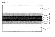
Fig. 1 shows a preferable example of embodiment of the composite film of the invention, wherein 1 is a substrate film, 2 is an organic layer, 3 is an inorganic layer, and 4 is an adhesive layer. - The contents of the invention are described in detail hereinunder. In this description, the numerical range expressed by the wording "a number to another number" means the range that falls between the former number indicating the lowermost limit of the range and the latter number indicating the uppermost limit thereof. In addition, "(meth)acrylate" means acrylate and methacrylate in the present specification.
- The composite film of the invention comprises a first gas barrier film, a second gas barrier film and an adhesive layer between the first gas barrier film and the second gas barrier film, wherein the first gas barrier film comprises a substrate film, at least one organic layer and at least one inorganic layer; the second gas barrier film comprises a substrate film, at least one organic layer and at least one inorganic layer; and the adhesive layer comprises a dry lamination adhesive and a metal alkoxide.
- By unifying the organic-inorganic laminate type gas barrier films through the adhesive layer containing a dry lamination adhesive and a metal alkoxide, the flexibility of the composite film is enhanced in addition that the barrier property of the composite film is enhanced.
-
Fig. 1 shows an example of embodiment of the composite film of the invention, wherein 1 stands for a substrate film, 2 stands for an organic layer, 3 stands for an inorganic layer, and 4 stands for an adhesive layer. Although numbers of the organic layer 2 and the inorganic layer 3 each are one in the embodiment, the numbers thereof may be each two or more. The number thereof is typically 2 to 30, preferably 3 to 20. The gas barrier film may comprise a constructing layer other than the organic layer and the inorganic layer. - In the embodiment, the inorganic layers in each of the gas barrier films of the composite film are adjacent to the adhesive layer, however, the organic layers therein may contact with the adhesive layer. In the invention, the inorganic layers in both of the gas barrier films are preferably adjacent to the adhesive layer.
- As mentioned above, the gas barrier film used in the invention necessarily comprises a substrate film and an organic layer and an inorganic layer which are provided on the substrate film. Such an organic layer and such an inorganic layer may be provided on the both side of the substrate film without diverting the scope of the invention. The gas barrier film of the invention is a film support having a barrier layer which has a function shutting oxygen, moisture, nitrogen oxides, sulfur oxides, ozone, or the like in the atmosphere.
- The organic layer in the invention is preferably an organic layer comprising an organic polymer as a main ingredient. Herein, the main ingredient means that the highest in ingredient composing the organic layer is an organic polymer, and generally 80% by weight or more in ingredient composing the organic layer is an organic polymer.
- The organic polymer is exemplified by an ultraviolet curable resin such as polyester, acrylic resin, methacrylic resin, methacrylic acid/maleic acid copolymer, polystyrene, transparent fluororesin, polyimide, fluoropolyimide, polyamide, polyamidimide, polyetherimide, cellulose acylate, polyurethane, polyether-ether ketone, polycarbonate, alicyclic polyolefin, polyarylate, polyether sulfone, polysulfone, fluorene ring-modified polycarbonate, alicyclic-modified polycarbonate, fluorene ring-modified polyester, acryloyl compound, etc..
- In the invention, the organic layer is preferably a layer obtainable by curing a polymerizable composition comprising polymerizable monomers.
- The polymerizable compound for use in the invention is preferably a radical polymerizable compound and/or a cationic polymerizable compound having an ether group as a functional group, more preferably a compound having an ethylenic unsaturated bond at the terminal or in the side chain thereof, and/or a compound having epoxy or oxetane at a terminal or in a side chain thereof. Of those, preferred is a compound having an ethylenic unsaturated bond at a terminal or in a side chain thereof. Examples of the compound having an ethylenic unsaturated bond at a terminal or in a side chain thereof include (meth)acrylate compounds, acrylamide compounds, styrene compound, maleic anhydride, etc, and preferably (meth)acrylate compounds and/or styrene compound, more preferably (meth)acrylate compounds.
- As (meth)acrylate compounds, preferred are (meth)acrylates, urethane-(meth)acrylates, polyester-(meth)acrylates, epoxy(meth)acrylates, etc.
- As styrene compounds, preferred are styrene, α-methylstyrene, 4-methylstyrene, divinylbenzene, 4-hydroxystyrene, 4-carboxystyrene, etc.
- Specific examples of (meth)acrylate compounds are mentioned below, to which, however, the invention should not be limited.


- In the case where the organic layer in the invention is formed by coating and curing a polymerizable composition comprising polymerizable compounds, the polymerizable composition may include a polymerization initiator. When a photopolymerization initiator is used, its amount is preferably at least 0.1 mol% of the total amount of the polymerizable compound, more preferably from 0.5 to 2 mol%. By setting the thus-designed composition, polymerization reaction though an active ingredient forming reaction may be suitably controlled. Examples of the photopolymerization initiator include Ciba Speciality Chemicals' commercial products, Irgacure series (e.g., Irgacure 651, Irgacure 754, Irgacure 184, Irgacure 2959, Irgacure 907, Irgacure 369, Irgacure 379, Irgacure 819), Darocure series (e.g., Darocure TPO, Darocure 1173), Quantacure PDO; Lamberti's commercial products, Ezacure series (e.g., Ezacure TZM, Ezacure TZT, Ezacure KTO46) and oligomer-type Esacure KIP series, etc.
- The method for forming the organic layer is not specifically defined. For example, the layer may be formed according to a solution coating method and a vacuum film formation method. The solution coating method is, for example, a dipping method, an air knife coating method, a curtain coating method, a roller coating method, a wire bar coating method, a gravure coating method, a slide coating method, or an extrusion coating method using a hopper as in
USP 2681294 . The vacuum film formation method is not specifically defined, but is preferably a film formation method by vapor deposition or plasma CVD. In the invention, the polymer may be applied for coating as its solution, or a hybrid coating method along with an inorganic material, as inJP-A 2000-323273 2004-25732 - In the invention, the polymerizable composition comprising a polymerizable compound is generally exposed to light for curing, and the light for exposure is generally a UV ray from a high-pressure mercury lamp or low-pressure mercury lamp. The radiation energy is preferably at least 0.1 J/cm2, more preferably at least 0.5 J/cm2. When acrylate or methacrylate is used as the polymerizable compound, such an acrylate or methacrylate may suffer from interference in polymerization owing to oxygen in air, and therefore, in its polymerization, the oxygen concentration or the oxygen partial pressure is preferably lowered. When the oxygen concentration in polymerization is lowered according to a nitrogen purging method, the oxygen concentration is preferably at most 2%, more preferably at most 0.5%. When the oxygen partial pressure in polymerization is lowered by a pressure reduction method, the whole pressure is preferably at most 1000 Pa, more preferably at most 100 Pa. Especially preferred is UV polymerization with at least 0.5 J/cm2 energy radiation under a condition of reduced pressure of at most 100 Pa.
- The organic layer is preferably smooth and has a hard surface. The rate of polymerization of monomer is at least 85%, more preferably at least 88%, even more preferably at least 90%, still more preferably at least 92%. The rate of polymerization as referred to herein means the ratio of the reacted polymerizable group to all the polymerizable group (acryloyl group and methacryloyl group) in the monomer mixture. The rate of polymerization may be quantitatively determined according to IR absorptiometry.
- The thickness of the organic layer is not specifically defined. However, when the layer is too thin, then its thickness could hardly keep uniformity; but when too thick, the layer may be cracked by external force applied thereto and its barrier-property may lower. From these viewpoints, the thickness of the organic layer is preferably from 50 nm to 2000 nm, more preferably from 200 nm to 1500 nm.
- As so mentioned in the above, the organic layer is preferably smooth. The mean roughness (Ra) at 1 µm square is preferably not more than 1 nm, more preferably not more than 0.5 nm. The surface of the organic layer is required not to have impurities and projections such as particles. Accordingly, it is desirable that the organic layer is formed in a clean room. The degree of cleanness is preferably at most class 10000, more preferably at most class 1000.
- Preferably, the hardness of the organic layer is higher. It is known that, when the hardness of the organic layer is high, then the inorganic layer may be formed smoothly and, as a result, the barrier level of the gas barrier film is thereby improved. The hardness of the organic layer may be expressed as a microhardness based on a nano-indentation method. The microhardness of the organic layer is preferably at least 100 N/mm, more preferably at least 150 N/mm.
- The inorganic layer is, in general, a layer of a thin film formed of a metal compound. For forming the inorganic layer, employable is any method capable of producing the intended thin film. For it, for example, suitable are physical vapor deposition (PVD) such as vapor evaporation process, sputtering process, ion plating process; various chemical vapor deposition (CVD); liquid phase growth process such as plating or sol-gel process. Not specifically defined, the component to be in the inorganic layer may be any one satisfies the above-mentioned requirements. Examples of the components include metal oxides, metal nitrides, metal carbides, metal oxinitrides and metal oxicabides. Preferred are oxides, nitrides, carbides, oxinitrides or oxicarbides comprising at least one metal selected from Si, Al, In, Sn, Zn, Ti, Cu, Ce and Ta. Of those, preferred are oxides, nitrides or oxinitrides of a metal selected from Si, Al, In, Sn, Zn and Ti; more preferred are metal oxides, nitrides or oxinitrides with Si or Al. These may comprise any other element as a subsidiary component.
- As a preferred embodiment of the invention, such that using a silicon oxide as a material of the inorganic layer and adding a silane coupling agent into the adhesive layer is exemplified. By employing such embodiment, the barrier property tends to be enhanced. Of the silicon oxide, further more preferably is silicon oxide represented by SiOx, wherein x is 0.9 to 1.5. Using of such an inorganic layer in an organic EL device tended to be avoided since the film to be formed colored. However, such coloration does not become a problem in the case of using for a solar cell. Preferably, the surface smoothness of the inorganic layer formed in the invention is less than 1 nm in terms of the mean surface roughness (Ra value) in 1 µm square, more preferably at most 0.5 nm. It is desirable that the inorganic layer is formed in a clean room. Preferably, the degree of cleanness is at most class 10000, more preferably at most class 1000.
- Not specifically defined, the thickness of the inorganic layer is generally within a range of from 5 to 500 nm/layer, preferably within a range of from 10 to 200 nm/layer.
- The organic layer and the inorganic layer may be laminated by repeated film formation to form the organic layer and the inorganic layer in a desired layer constitution. When the inorganic layer is formed according to a vacuum film formation process such as sputtering process, vacuum evaporation process, ion plating process or plasma CVD, then it is desirable that the organic layer is also formed according to a vacuum film formation process such as the above-mentioned flash vapor deposition process. While the inorganic layer and the organic layer are formed, it is especially desirable that the organic layer and the inorganic layer are laminated all the time in a vacuum of at most 1000 Pa, not restoring the pressure to an atmospheric pressure during the film formation. More preferably, the pressure is at most 100 Pa, even more preferably at most 50 Pa, still more preferably at most 20 Pa.
- The barrier laminate of the invention may have a functional layer on the barrier laminate or in any other position without deriving the scope of the invention. The functional layer is described in detail in
JP-A 2006-289627 - In the gas barrier film of the invention, the substrate film is generally a plastic film. Not specifically defined in point of the material and the thickness thereof, the plastic film usable herein may be any one capable of supporting a laminate of an organic layer and an inorganic layer; and it may be suitably selected depending on the use and the object thereof. Concretely, the plastic film includes thermoplastic resins such as polyester resin, methacryl resin, methacrylic acid-maleic anhydride copolymer, polystyrene resin, transparent fluororesin, polyimide, fluoropolyimide resin, polyamide resin, polyamidimide resin, polyetherimide resin, cellulose acylate resin, polyurethane resin, polyether ether ketone resin, polycarbonate resin, alicyclic polyolefin resin, polyarylate resin, polyether sulfone resin, polysulfone resin, cycloolefin copolymer, fluorene ring-modified polycarbonate resin, alicyclic-modified polycarbonate resin, fluorene ring-modified polyester resin, acryloyl compound.
- When the composite film of the invention is used as a substrate of a device such as an organic EL device to be mentioned hereinunder, it is desirable that the plastic film is formed of a heat-resistant material. Concretely, the plastic film is preferably formed of a heat-resistant transparent material having a glass transition temperature (Tg) of not lower than 100°C and/or a linear thermal expansion coefficient of at least 40 ppm/°C. Tg and the linear expansion coefficient may be controlled by the additives to the material. The thermoplastic resin of the type includes, for example, polyethylene naphthalate (PEN: 120°C), polycarbonate (PC: 140°C), alicyclic polyolefin (e.g., Nippon Zeon's Zeonoa 1600: 160°C), polyarylate (PAr: 210°C), polyether sulfone (PES: 220°C), polysulfone (PSF: 190°C), cycloolefin copolymer (COC, compound described in
JP-A 2001-150584 JP-A 2000-227603 JP-A 2000-227603 JP-A 2002-80616 - When the composite film of the invention is used for purpose requesting transparency, the plastic film is transparent, or that is, its light transmittance is generally at least 80%, preferably at least 85%, more preferably at least 90%. The light transmittance may be measured according to the method described in JIS-K7105.
- Not specifically defined, the thickness of the plastic film for use in the gas barrier film of the invention may be suitably selected depending on its use. Typically, the thickness may be from 1 to 800 µm, preferably from 10 to 200 µm. The plastic film may have a functional layer such as a transparent conductive layer, a primer layer, etc. The functional layer is described in detail in
JP-A 2006-289627 - The adhesive layer in the invention comprises a dry lamination adhesive and a metal alkoxide. By adding such a metal alkoxide into the adhesive layer, the composite film excellent in flexibility over a long period of time is obtained. The composite film can maintain its favorable barrier property even when it has been placed in conditions of heat and humidity over a long period of time.
- The dry lamination adhesive is preferably a polyurethane series adhesive, more preferably a two-liquid mixing polyurethane series adhesive.
- The metal alkoxide preferably comprises silicon atom, aluminum atom, titanium atom, zirconium atom, or magnesium atom as a metal component, and more preferably comprises silicon atom as a metal component.
- The molecular weight of the metal alkoxide is preferably 130 to 500, more preferably 200 to 300. The metal alkoxide in the adhesive layer preferably occupies 5 to 30% by weight of a total amount of the adhesive layer.
- The metal alkoxide and the dry lamination adhesive occupies 90% by weight or more of a total amount of the adhesive layer, more preferably 99% by weight or more of a total amount of the adhesive layer.
- Thickness for the composite film of the invention is not specifically limited, for example, the thickness is 10 to 500 µm, preferably 25 to 400 µm.
- Water vapor permeability at 40°C and 90% relative humidity of the composite film of the invention is, for example, 0.05 g/m2/day or less, further 3e-3 to 1e-4 g/m2/day.
- The composite film of the invention can be used for sealing devices which deteriorate by water moisture, oxygen, and the like, even if used under at ordinary temperatures and pressures over long years. The devices are exemplified by a solar cell, an electronic paper, and the like.
- The composite film of the invention can be used as a front sheet for a solar cell or a back sheet for a solar cell. The solar cell generally has an active part which practically operates as a solar cell between a pair of substrates. In the invention, the composite film of the invention may be used as one or both of the pair of substrates.
- The solar cell for which the composite film of the invention is favorably used is not specifically defined. For example, they include single crystal silicon-based solar cell devices, polycrystalline silicon-based solar cell devices, single-junction or tandem-structure amorphous silicon-based solar cell devices, gallium-arsenic (GaAs), indium-phosphorus (InP) or the like III-V Group compound semiconductor-based solar cell devices, cadmium-tellurium (CdTe) or the like II-VI Group compound semiconductor-based solar cell devices, copper/indium/selenium (CIS-based), copper/indium/gallium/selenium (CIGS-based), copper/indium/gallium/selenium/sulfur (CIGSS-based) or the like I-III-VI Group compound semiconductor-based solar cell devices, dye-sensitized solar cell devices, organic solar cell devices, etc. Above all, in the invention, the solar cell devices are preferably copper/indium/selenium (CIS-based), copper/indium/gallium/selenium (CIGS-based), copper/indium/gallium/selenium/sulfur (CIGSS-based) or the like I-III-VI Group compound semiconductor-based solar cell devices.
- The composite film of the invention can be used in an electronic paper. The electronic paper is a reflection-type electronic display capable of attaining a high precision and a high contrast.
- The electronic paper has a display media and a TFT driving the display media on a substrate. Any known display media can be used in the electronic paper. For example, any display media of electophoretic-type, electopowder flight-type, charged tonner-type, electrochromic type can be preferably used. Among them, electophoretic display media is more preferable and microcapsule-type electophoretic display media is particularly preferable. The electophoretic display media has a plural number of capsules and each capsule has at least one particle capable of moving in a suspension flow. The at least one particle is preferably an electrophoretic particle or a spinning ball. The electrophretic display media has a first plane and a second plane that are placed in parallel, and an image is displayed through one of the two planes.
- A TFT formed on a substrate comprises a gate electrode, gate insulating layer, an active layer, a source electrode and a drain electrode. A TFT also comprises a resistance layer between the active layer and the source electrode and/or between the active layer and the drain electrode to attain electric connection.
- When a color display with a high precision is produced, TFT's are preferably formed on a color filter to precisely align them. Normal TFT with a low electric efficiency can not be down-sized much while obtaining the necessary driving current, and when a high precision display is pursued, the rate of the area for the TFT in a pixel must be high. When the rate of the area for the TFT is high, the rate of the opening area and contrast are low. Even when a transparent amorphous IGZO-type TFT is used, light transmittance is not 100% and reduction of contrast is unavoidable. Use of the TFT disclosed in
JP-A 2009-21554 - Other applications of the invention are thin-film transistors as in
JP-T H10-512104 JP-A 5-127822 2002-48913 JP-A-2002-865554 JP-A-2007-30387 - The characteristics of the invention are described more concretely with reference to the following Examples. In the following Examples, the material used, its amount and the ratio, the details of the treatment and the treatment process may be suitably modified or changed not overstepping the sprit and the scope of the invention. Accordingly, the invention should not be limitatively interpreted by the Examples mentioned below.
- PET film (COSMOSHINE A4300, having thickness of 100 µm) was cut into 10 cm square. On the surface thereof, an organic layer and an inorganic layer were formed by the following process.
- On the PET film, a polymerizable composition consisting of trimethylolpropane triacrylate (TMPTA, manufactured by DIC), 0.6 g of an ultraviolet polymerization initiator (manufactured by Chiba Specialty. Chemicals Inc., Irgacure 184), and 190 g of propylene glycol monomethyl ether acetate was coated using a wire bar, and was cured through irradiation with UV rays from a high-pressure mercury lamp (the total dose is 1.5 J/cm2) under oxygen concentration of 0.1 % or less by nitrogen substitution, thereby producing the organic layer having a thickness of about 1 µm.
- Using a sputtering device or a deposition device, an inorganic layer (silicon oxide layer) was formed on the organic layer. Silicon as target, argon as flow gas, and oxygen as reactive gas were used. The formation pressure was 0.1 Pa, and the attained film thickness was 60 nm. Thus the inorganic layer was laminated on the organic layer to form a gas barrier film.
- The adhesive composition was prepared by adding silane coupling agent (manufactured by TORAY dowcorning, Z-6044) into a two-liquid mixing urethane series adhesive(manufactured by Dainichiseika Color & Chemicals Mfg.Co. ,Ltd, main agent:E-372, curing agent:C-76) as an adhesive. The adhesive composition was composed of 90% by weight of the adhesive and 10% by weight of the silane coupling agent.
- On the inorganic layer of the gas barrier film as obtained above, the above adhesive composition was coated by a bar coating method, and then, on the surface thereof, another gas barrier film as obtained above was further stacked. The stacking was carried out so that each of the inorganic layer sides contacted with the adhesive layer. Thus, the composite film was obtained.
- Composite films of Examples and Comparative Examples were formed according to the same method, except that each of the construction was replaced as shown in the table below. In Example 3, the amount to be added of the silane coupling agent was changed. In Example 4, aluminum tri-iso isopropoxide was added in place of the silane coupling agent.
- Water vapor permeability and flexibility for the composite films obtained in Examples and Comparative Examples above were measured and evaluated according to the following methods. In addition, water vapor permeability and flexibility of the composite films after they were placed at 85°C and 85% RH for 1000 hours were measured and evaluated.
- T-type peeling test for the composite films was carried out according to JIS K6854.
- The water vapor permeability were measured according to the method described in G. NISATO, P.C.P. BOUTEN, P.J. SLIKKERVEER, et al.; SID Conference Record of the International Display Research Conference 1435-1438. The measure was carried out at 40°C and 90 % RH. The results were shown in below table.
- The composite film was subjected to bending in 180° using a mandrill having a diameter of 20 mm, which was repeated ten times. Then, the water vapor permeability of the composite film was measured and evaluated according to the above method.
- Each of the composite films as formed above was placed at 85°C and 85% RH for 250 hours, and then the adhesiveness and the water vapor permeability were measured and evaluated according to the above methods.
[Table 1] Organic Layer Thickness of Organic Layer(µm) Method for forming Inorganic Layer Metal alkoxide Adhesiveness WVP WVP after bending Adhesiveness (over time) WVP (over time) (N/15mm) (g/m2/day) (g/m2/day) (N/15mm) (g/m2/day) Example 1 TMPTA 1 Sputtering Added 5.8 4.3 e-4 5.1e-4 5.8 5.3 e-4 Example 2 TMPTA 1 Deposition Added 5.4 3.1e-3 3.3e-3 5.3 3.5-3 Example 3 TMPTA 1 Sputtering Added 5.6 4.8 e-4 5.5e-4 5.3 7.1 e-4 Example 4 TMPTA 1 Sputtering Added 5.5 4.9e-4 5.8e-4 5.0 7.8e-4 Com.Example 1 TMPTA 1 Sputtering Not added 5.3 4.2 e-4 8.1e-4 4.9 1.1e-3 Com.Example 2 Not provided - Sputtering Added 6.1 1.2e-2 5.5e-2 5.9 3.3e-2 Com.Example 3 Not provided - Sputtering Not added 5.8 1.1e-2 5.2e-2 3.1 4.4e-2 Com.Example 4 TMPTA 1 Deposition Not added 5.2 3.5e-3 7.2e-3 3.0 9.9e-3 Com.Example 5 Not provided - Deposition Added 5.5 4.2 e-2 1.2e-1 5.4 9.7e-2 Com.Example 6 Not provided - Deposition Not added 5.0 4.4e-2 9.8e-2 2.9 9.2e-2 - In the above table, WVP means the water vapor permeability. As is clear from the above table, it was found that reduction for the water vapor permeability after the bending test and reduction for the water vapor permeability after the humidity and heat test were controlled by using the adhesive comprising the silane coupling agent in the case where the organic-inorganic laminate type gas barrier films are stuck to each other (Examples 1 to 3). On the other hand, it was found that the water vapor permeability after the bending test and the water vapor permeability after the humidity and heat were reduced in the case where the adhesive does not comprise any metal alkoxide (Comparative Examples 1 and 4).
- Similarly, it was found that the water vapor permeability after the bending test and the water vapor permeability after the humidity and heat test reduced regardless of comprising the silane coupling agent, in the case where the gas barrier films comprising only the inorganic layer are stuck to each other (Comparative Examples 2, 3, 5 and 6). This means that, although the adhesive agent comprising the silane coupling agent enhances the adhesiveness, thereby rather enhancing the barrier property, the adhesive agent comprising the silane coupling agent does not advantageously affect the moisture and heat resistance and the flexibility.
- In the case where the gas barrier films comprising only the inorganic layer are stuck to each other, the water vapor permeability after the bending test and the water vapor permeability after the humidity and heat test reduced regardless of comprising the silane coupling agent. On the other hand, in the case where the organic-inorganic laminate type gas barrier films are stuck to each other, the water vapor permeability after the bending test and the water vapor permeability after the humidity and heat test can be controlled to reduce only by using the adhesive comprising the silane coupling agent. That is, the invention is based on completely different technique from the conventional laminating of films and the achievement thereof is really great.
Claims (14)
- A composite film comprising a first gas barrier film, a second gas barrier film and an adhesive layer between the first gas barrier film and the second gas barrier film, wherein the first gas barrier film comprises a substrate film, at least one organic layer and at least one inorganic layer; the second gas barrier film comprises a substrate film, at least one organic layer and at least one inorganic layer; and the adhesive layer comprises a dry lamination adhesive and a metal alkoxide.
- The composite film according to Claim 1, wherein the adhesive layer is in contact with the inorganic layer of the first gas barrier film and the inorganic layer of the second gas barrier film.
- The composite film according to Claim 1 or 2, wherein the inorganic layer of the first gas barrier film is adjacent to the adhesive layer; and the inorganic layer of the second gas barrier film is adjacent to the adhesive layer.
- The composite film according to any one of Claims 1 to 3, wherein the adhesive layer comprises the metal alkoxide in an amount of 5 to 30% by weight of the adhesive layer.
- The composite film according to any one of Claims 1 to 4, wherein the metal alkoxide is a silane coupling agent.
- The composite film according to any one of Claims 1 to 5, wherein at least one of the inorganic layers comprises an aluminum-containing compound and/or a silicon-containing compound.
- The composite film according to any one of Claims 1 to 6, wherein the dry lamination adhesive is a polyurethane series adhesive.
- The composite film according to any one of Claims 1 to 7, wherein at least one of the organic layers comprises an ultraviolet curable resin.
- The composite film according to any one of Claims 1 to 8, wherein at least one of the organic layers is obtained by curing a polymerizable composition comprising a (meth)acrylate.
- The composite film according to any one of Claims 1 to 9, wherein at least one of the substrate films is a polyester series resin film.
- The composite film according to any one of Claims 1 to 10, wherein the dry lamination adhesive is a two-liquid mixing polyurethane series adhesive.
- The composite film according to any one of Claims 1 to 11, wherein the metal alkoxide is a silane coupling agent; and at least one of the inorganic layers comprises a silicon oxide.
- A member for a solar cell, comprising the composite film of any one of Claims 1 to 12.
- A method for manufacturing of a composite film, which comprises laminating a first gas barrier film comprising a substrate, at least one organic layer and at least one inorganic layer and a second gas barrier film comprising a substrate, at least one organic layer and at least one inorganic layer through an adhesive layer comprising a dry lamination adhesive and a metal alkoxide, and then curing the adhesive layer.
Applications Claiming Priority (1)
| Application Number | Priority Date | Filing Date | Title |
|---|---|---|---|
| JP2009201314A JP5414426B2 (en) | 2009-09-01 | 2009-09-01 | Composite film |
Publications (2)
| Publication Number | Publication Date |
|---|---|
| EP2289983A1 EP2289983A1 (en) | 2011-03-02 |
| EP2289983B1 true EP2289983B1 (en) | 2012-01-18 |
Family
ID=43128305
Family Applications (1)
| Application Number | Title | Priority Date | Filing Date |
|---|---|---|---|
| EP20100174842 Not-in-force EP2289983B1 (en) | 2009-09-01 | 2010-09-01 | Composite film |
Country Status (4)
| Country | Link |
|---|---|
| US (1) | US20110052893A1 (en) |
| EP (1) | EP2289983B1 (en) |
| JP (1) | JP5414426B2 (en) |
| AT (1) | ATE541882T1 (en) |
Families Citing this family (21)
| Publication number | Priority date | Publication date | Assignee | Title |
|---|---|---|---|---|
| JP5281986B2 (en) * | 2009-08-26 | 2013-09-04 | 富士フイルム株式会社 | Laminated film and composite film |
| TWI552883B (en) * | 2011-07-25 | 2016-10-11 | Lintec Corp | Gas barrier film laminates and electronic components |
| KR101985983B1 (en) * | 2011-08-04 | 2019-06-04 | 쓰리엠 이노베이티브 프로퍼티즈 컴파니 | Method of making delamination resistant assemblies |
| WO2013019695A2 (en) | 2011-08-04 | 2013-02-07 | 3M Innovative Properties Company | Edge protected barrier assemblies |
| JP2013226758A (en) * | 2012-04-26 | 2013-11-07 | Konica Minolta Inc | Method for manufacturing gas barrier film |
| JP5983454B2 (en) * | 2012-12-26 | 2016-08-31 | コニカミノルタ株式会社 | Gas barrier film |
| WO2014136616A1 (en) * | 2013-03-08 | 2014-09-12 | 富士フイルム株式会社 | Organic el laminate |
| JP6333516B2 (en) * | 2013-03-25 | 2018-05-30 | 興人フィルム&ケミカルズ株式会社 | Gas barrier film and production method |
| JP2016525234A (en) * | 2013-07-24 | 2016-08-22 | スリーエム イノベイティブ プロパティズ カンパニー | Adhesive barrier film structure |
| WO2015133286A1 (en) * | 2014-03-04 | 2015-09-11 | コニカミノルタ株式会社 | Sealing method for functional elements, and functional element sealed by said sealing method |
| KR101760225B1 (en) * | 2014-07-18 | 2017-07-20 | 도판 인사츠 가부시키가이샤 | Protective film for wavelength conversion sheet, wavelength conversion sheet and backlight unit |
| EP3208520B1 (en) | 2014-10-16 | 2023-05-03 | Toppan Printing Co., Ltd. | Quantum dot protective film, quantum dot film using same, and backlight unit |
| JPWO2016167295A1 (en) * | 2015-04-15 | 2018-02-08 | 凸版印刷株式会社 | Transparent gas barrier laminated film and electronic paper using the same |
| JP2016213369A (en) * | 2015-05-12 | 2016-12-15 | 凸版印刷株式会社 | Protective film for wavelength conversion sheet, wavelength conversion sheet, and backlight unit |
| US10608203B2 (en) | 2015-07-23 | 2020-03-31 | Sharp Kabushiki Kaisha | Silicon oxide sealing layer for electroluminescent device |
| JP7000156B2 (en) * | 2015-09-07 | 2022-02-04 | 凸版印刷株式会社 | Protective film for wavelength conversion sheet, wavelength conversion sheet and backlight unit |
| JP6790345B2 (en) * | 2015-10-27 | 2020-11-25 | 凸版印刷株式会社 | Wavelength conversion sheet |
| WO2017073671A1 (en) * | 2015-10-27 | 2017-05-04 | 凸版印刷株式会社 | Light emitting body protective film, wavelength conversion sheet, backlight unit and electroluminescent light emitting unit |
| JP6202074B2 (en) * | 2015-11-20 | 2017-09-27 | 凸版印刷株式会社 | Wavelength conversion sheet |
| CN111834481B (en) * | 2020-07-24 | 2021-10-12 | 东方日升(义乌)新能源有限公司 | Packaging method of solar glass assembly |
| CN112940325B (en) * | 2021-02-24 | 2022-07-12 | 辽宁万鑫富利新材料有限公司 | Degradable plastic composite film and preparation process thereof |
Family Cites Families (30)
| Publication number | Priority date | Publication date | Assignee | Title |
|---|---|---|---|---|
| BE513714A (en) * | 1951-08-23 | 1900-01-01 | ||
| JPH05127822A (en) | 1991-10-30 | 1993-05-25 | Daicel Chem Ind Ltd | Touch panel |
| JP2733180B2 (en) * | 1993-02-09 | 1998-03-30 | 東洋製罐株式会社 | Flexible packaging laminate, method for producing the same, and adhesive used therefor |
| US6485726B1 (en) * | 1995-01-17 | 2002-11-26 | The Brigham And Women's Hospital, Inc. | Receptor specific transepithelial transport of therapeutics |
| GB9521855D0 (en) | 1995-10-25 | 1996-01-03 | Philips Electronics Nv | Manufacture of electronic devices comprising thin-film circuitry |
| US6335479B1 (en) * | 1998-10-13 | 2002-01-01 | Dai Nippon Printing Co., Ltd. | Protective sheet for solar battery module, method of fabricating the same and solar battery module |
| JP2000332277A (en) * | 1999-05-17 | 2000-11-30 | Dainippon Printing Co Ltd | Solar battery module and protective sheet therefor |
| JP2000227603A (en) | 1998-11-30 | 2000-08-15 | Teijin Ltd | Liquid crystal display device and transparent conductive substrate suitable for the same |
| JP2000323273A (en) | 1999-05-07 | 2000-11-24 | Dainippon Printing Co Ltd | Electroluminescent element |
| US6353479B1 (en) * | 1999-06-29 | 2002-03-05 | Hewlett-Packard Company | Media-type encoding and print mode selection |
| JP2001150584A (en) | 1999-11-29 | 2001-06-05 | Nippon Zeon Co Ltd | Conductive substrate, and display element using the same |
| JP2001171035A (en) * | 1999-12-17 | 2001-06-26 | Dainippon Printing Co Ltd | Laminated material |
| JP3958486B2 (en) | 2000-01-31 | 2007-08-15 | 大日精化工業株式会社 | Two-component curable resin composition and laminating adhesive |
| JP2002080616A (en) | 2000-06-30 | 2002-03-19 | Sumitomo Bakelite Co Ltd | Polymer film for display element and substrate for display element using the same |
| JP2002048913A (en) | 2000-08-04 | 2002-02-15 | Fuji Photo Film Co Ltd | Retardation film, circularly polarizing plate and reflective liquid crystal display device |
| JP2002275448A (en) | 2001-03-16 | 2002-09-25 | Toyobo Co Ltd | Adhesive for inorganic vapor-deposited film |
| US6579472B2 (en) * | 2001-07-27 | 2003-06-17 | The Boeing Company | Corrosion inhibiting sol-gel coatings for metal alloys |
| JP4402864B2 (en) | 2002-06-27 | 2010-01-20 | 富士フイルム株式会社 | Gas barrier film |
| JP4420375B2 (en) | 2003-03-20 | 2010-02-24 | 東洋モートン株式会社 | Laminate film laminate |
| JP4716773B2 (en) | 2005-04-06 | 2011-07-06 | 富士フイルム株式会社 | Gas barrier film and organic device using the same |
| JP2007030387A (en) | 2005-07-28 | 2007-02-08 | Fujifilm Corp | Film substrate having barrier property and organic electroluminescence element using the same |
| ITTO20050718A1 (en) * | 2005-10-10 | 2007-04-11 | Consorzio Interuniverstario | LAMINATED MATERIAL WITH HIGH BARRIER EFFECT ON THE OXYGEN |
| JP2008130647A (en) * | 2006-11-17 | 2008-06-05 | Toppan Printing Co Ltd | Backseat for solar-cell module, and solar-cell module using the backseat |
| JP5339772B2 (en) | 2007-06-11 | 2013-11-13 | 富士フイルム株式会社 | Electronic display |
| JP2009067040A (en) * | 2007-08-21 | 2009-04-02 | Fujifilm Corp | Composite gas-barrier film and display element using the same |
| EP2033986A1 (en) * | 2007-09-03 | 2009-03-11 | Alcan Technology & Management Ltd. | Packaging part and method for its production |
| JP5140376B2 (en) * | 2007-10-16 | 2013-02-06 | 富士フイルム株式会社 | Gas barrier film and environmentally sensitive device |
| EP2050780A3 (en) * | 2007-10-16 | 2009-12-16 | Fujifilm Corporation | Barrier laminate, barrier film substrate, device, and method for producing barrier laminate |
| KR101639071B1 (en) * | 2008-10-30 | 2016-07-12 | 삼성전자주식회사 | Multilayered film, method of making the same, and encapsulated structure including the same |
| EP2361288B1 (en) * | 2008-12-19 | 2016-03-30 | Fraunhofer-Gesellschaft zur Förderung der angewandten Forschung e.V. | High barrier compound and method for its production |
-
2009
- 2009-09-01 JP JP2009201314A patent/JP5414426B2/en not_active Expired - Fee Related
-
2010
- 2010-08-31 US US12/873,004 patent/US20110052893A1/en not_active Abandoned
- 2010-09-01 AT AT10174842T patent/ATE541882T1/en active
- 2010-09-01 EP EP20100174842 patent/EP2289983B1/en not_active Not-in-force
Also Published As
| Publication number | Publication date |
|---|---|
| EP2289983A1 (en) | 2011-03-02 |
| ATE541882T1 (en) | 2012-02-15 |
| US20110052893A1 (en) | 2011-03-03 |
| JP5414426B2 (en) | 2014-02-12 |
| JP2011051195A (en) | 2011-03-17 |
Similar Documents
| Publication | Publication Date | Title |
|---|---|---|
| EP2289983B1 (en) | Composite film | |
| EP2298551B1 (en) | Gas barrier film and device | |
| US9893317B2 (en) | Barrier laminate and gas barrier film | |
| EP2749409B1 (en) | Barrier laminate, and gas barrier film | |
| EP2128191B1 (en) | Barrier laminate, gas barrier film, device, and method for producing barrier laminate | |
| US8197946B2 (en) | Barrier laminate, barrier film substrate, methods for producing them, and device | |
| EP2529926A1 (en) | Gas barrier film, production method therefor, and device using same | |
| US20100003480A1 (en) | Barrier laminate, gas barrier film, device and optical member | |
| EP2289984A1 (en) | Laminate film and composite film | |
| JP5966821B2 (en) | Gas barrier laminated film | |
| EP2228846A1 (en) | Barrier laminate, gas barrier film, and device using the same | |
| US8758889B2 (en) | Gas barrier film and device | |
| EP2138532B1 (en) | Barrier laminate, gas barrier film and device | |
| WO2019151495A1 (en) | Gas-barrier film and manufacturing method therefor | |
| WO2011027902A1 (en) | Barrier laminate, gas barrier film and method for manufacturing the barrier laminate | |
| EP2128192B1 (en) | Barrier laminate, gas barrier film and device using the same | |
| JP2012025099A (en) | Gas barrier film and electronic device | |
| EP2042545B1 (en) | Barrier film substrate and method for producing same, and organic device | |
| JP2003211579A (en) | Transparent steam barrier film | |
| JP5757170B2 (en) | Method for producing gas barrier film | |
| EP3872226A1 (en) | Barrier film | |
| EP1958981B1 (en) | Barrier laminate, barrier film substrate, methods for producing them, and device | |
| JP2023094053A (en) | Adhesive sheet, laminate for image display devices and image display device, and adhesive composition |
Legal Events
| Date | Code | Title | Description |
|---|---|---|---|
| PUAI | Public reference made under article 153(3) epc to a published international application that has entered the european phase |
Free format text: ORIGINAL CODE: 0009012 |
|
| AK | Designated contracting states |
Kind code of ref document: A1 Designated state(s): AL AT BE BG CH CY CZ DE DK EE ES FI FR GB GR HR HU IE IS IT LI LT LU LV MC MK MT NL NO PL PT RO SE SI SK SM TR |
|
| AX | Request for extension of the european patent |
Extension state: BA ME RS |
|
| 17P | Request for examination filed |
Effective date: 20110520 |
|
| GRAP | Despatch of communication of intention to grant a patent |
Free format text: ORIGINAL CODE: EPIDOSNIGR1 |
|
| RIC1 | Information provided on ipc code assigned before grant |
Ipc: H01L 31/0216 20060101ALI20110609BHEP Ipc: C08J 7/04 20060101ALI20110609BHEP Ipc: C08J 5/18 20060101AFI20110609BHEP |
|
| RIN1 | Information on inventor provided before grant (corrected) |
Inventor name: OOUCHI, RYOU |
|
| GRAS | Grant fee paid |
Free format text: ORIGINAL CODE: EPIDOSNIGR3 |
|
| RIN1 | Information on inventor provided before grant (corrected) |
Inventor name: OOUCHI, RYOU |
|
| GRAA | (expected) grant |
Free format text: ORIGINAL CODE: 0009210 |
|
| RAP1 | Party data changed (applicant data changed or rights of an application transferred) |
Owner name: FUJIFILM CORPORATION |
|
| AK | Designated contracting states |
Kind code of ref document: B1 Designated state(s): AL AT BE BG CH CY CZ DE DK EE ES FI FR GB GR HR HU IE IS IT LI LT LU LV MC MK MT NL NO PL PT RO SE SI SK SM TR |
|
| REG | Reference to a national code |
Ref country code: GB Ref legal event code: FG4D |
|
| REG | Reference to a national code |
Ref country code: CH Ref legal event code: EP |
|
| REG | Reference to a national code |
Ref country code: AT Ref legal event code: REF Ref document number: 541882 Country of ref document: AT Kind code of ref document: T Effective date: 20120215 Ref country code: IE Ref legal event code: FG4D |
|
| REG | Reference to a national code |
Ref country code: NL Ref legal event code: T3 |
|
| REG | Reference to a national code |
Ref country code: DE Ref legal event code: R096 Ref document number: 602010000694 Country of ref document: DE Effective date: 20120322 |
|
| LTIE | Lt: invalidation of european patent or patent extension |
Effective date: 20120118 |
|
| PG25 | Lapsed in a contracting state [announced via postgrant information from national office to epo] |
Ref country code: HR Free format text: LAPSE BECAUSE OF FAILURE TO SUBMIT A TRANSLATION OF THE DESCRIPTION OR TO PAY THE FEE WITHIN THE PRESCRIBED TIME-LIMIT Effective date: 20120118 Ref country code: NO Free format text: LAPSE BECAUSE OF FAILURE TO SUBMIT A TRANSLATION OF THE DESCRIPTION OR TO PAY THE FEE WITHIN THE PRESCRIBED TIME-LIMIT Effective date: 20120418 Ref country code: IS Free format text: LAPSE BECAUSE OF FAILURE TO SUBMIT A TRANSLATION OF THE DESCRIPTION OR TO PAY THE FEE WITHIN THE PRESCRIBED TIME-LIMIT Effective date: 20120518 Ref country code: BE Free format text: LAPSE BECAUSE OF FAILURE TO SUBMIT A TRANSLATION OF THE DESCRIPTION OR TO PAY THE FEE WITHIN THE PRESCRIBED TIME-LIMIT Effective date: 20120118 Ref country code: LT Free format text: LAPSE BECAUSE OF FAILURE TO SUBMIT A TRANSLATION OF THE DESCRIPTION OR TO PAY THE FEE WITHIN THE PRESCRIBED TIME-LIMIT Effective date: 20120118 Ref country code: BG Free format text: LAPSE BECAUSE OF FAILURE TO SUBMIT A TRANSLATION OF THE DESCRIPTION OR TO PAY THE FEE WITHIN THE PRESCRIBED TIME-LIMIT Effective date: 20120418 |
|
| PG25 | Lapsed in a contracting state [announced via postgrant information from national office to epo] |
Ref country code: PT Free format text: LAPSE BECAUSE OF FAILURE TO SUBMIT A TRANSLATION OF THE DESCRIPTION OR TO PAY THE FEE WITHIN THE PRESCRIBED TIME-LIMIT Effective date: 20120518 Ref country code: LV Free format text: LAPSE BECAUSE OF FAILURE TO SUBMIT A TRANSLATION OF THE DESCRIPTION OR TO PAY THE FEE WITHIN THE PRESCRIBED TIME-LIMIT Effective date: 20120118 Ref country code: FI Free format text: LAPSE BECAUSE OF FAILURE TO SUBMIT A TRANSLATION OF THE DESCRIPTION OR TO PAY THE FEE WITHIN THE PRESCRIBED TIME-LIMIT Effective date: 20120118 Ref country code: GR Free format text: LAPSE BECAUSE OF FAILURE TO SUBMIT A TRANSLATION OF THE DESCRIPTION OR TO PAY THE FEE WITHIN THE PRESCRIBED TIME-LIMIT Effective date: 20120419 Ref country code: PL Free format text: LAPSE BECAUSE OF FAILURE TO SUBMIT A TRANSLATION OF THE DESCRIPTION OR TO PAY THE FEE WITHIN THE PRESCRIBED TIME-LIMIT Effective date: 20120118 |
|
| REG | Reference to a national code |
Ref country code: AT Ref legal event code: MK05 Ref document number: 541882 Country of ref document: AT Kind code of ref document: T Effective date: 20120118 |
|
| PG25 | Lapsed in a contracting state [announced via postgrant information from national office to epo] |
Ref country code: CY Free format text: LAPSE BECAUSE OF FAILURE TO SUBMIT A TRANSLATION OF THE DESCRIPTION OR TO PAY THE FEE WITHIN THE PRESCRIBED TIME-LIMIT Effective date: 20120118 |
|
| PG25 | Lapsed in a contracting state [announced via postgrant information from national office to epo] |
Ref country code: SI Free format text: LAPSE BECAUSE OF FAILURE TO SUBMIT A TRANSLATION OF THE DESCRIPTION OR TO PAY THE FEE WITHIN THE PRESCRIBED TIME-LIMIT Effective date: 20120118 Ref country code: SE Free format text: LAPSE BECAUSE OF FAILURE TO SUBMIT A TRANSLATION OF THE DESCRIPTION OR TO PAY THE FEE WITHIN THE PRESCRIBED TIME-LIMIT Effective date: 20120118 Ref country code: EE Free format text: LAPSE BECAUSE OF FAILURE TO SUBMIT A TRANSLATION OF THE DESCRIPTION OR TO PAY THE FEE WITHIN THE PRESCRIBED TIME-LIMIT Effective date: 20120118 Ref country code: CZ Free format text: LAPSE BECAUSE OF FAILURE TO SUBMIT A TRANSLATION OF THE DESCRIPTION OR TO PAY THE FEE WITHIN THE PRESCRIBED TIME-LIMIT Effective date: 20120118 Ref country code: DK Free format text: LAPSE BECAUSE OF FAILURE TO SUBMIT A TRANSLATION OF THE DESCRIPTION OR TO PAY THE FEE WITHIN THE PRESCRIBED TIME-LIMIT Effective date: 20120118 Ref country code: RO Free format text: LAPSE BECAUSE OF FAILURE TO SUBMIT A TRANSLATION OF THE DESCRIPTION OR TO PAY THE FEE WITHIN THE PRESCRIBED TIME-LIMIT Effective date: 20120118 |
|
| PLBE | No opposition filed within time limit |
Free format text: ORIGINAL CODE: 0009261 |
|
| STAA | Information on the status of an ep patent application or granted ep patent |
Free format text: STATUS: NO OPPOSITION FILED WITHIN TIME LIMIT |
|
| PG25 | Lapsed in a contracting state [announced via postgrant information from national office to epo] |
Ref country code: SK Free format text: LAPSE BECAUSE OF FAILURE TO SUBMIT A TRANSLATION OF THE DESCRIPTION OR TO PAY THE FEE WITHIN THE PRESCRIBED TIME-LIMIT Effective date: 20120118 Ref country code: IT Free format text: LAPSE BECAUSE OF FAILURE TO SUBMIT A TRANSLATION OF THE DESCRIPTION OR TO PAY THE FEE WITHIN THE PRESCRIBED TIME-LIMIT Effective date: 20120118 |
|
| 26N | No opposition filed |
Effective date: 20121019 |
|
| PG25 | Lapsed in a contracting state [announced via postgrant information from national office to epo] |
Ref country code: AT Free format text: LAPSE BECAUSE OF FAILURE TO SUBMIT A TRANSLATION OF THE DESCRIPTION OR TO PAY THE FEE WITHIN THE PRESCRIBED TIME-LIMIT Effective date: 20120118 |
|
| REG | Reference to a national code |
Ref country code: DE Ref legal event code: R097 Ref document number: 602010000694 Country of ref document: DE Effective date: 20121019 |
|
| PG25 | Lapsed in a contracting state [announced via postgrant information from national office to epo] |
Ref country code: ES Free format text: LAPSE BECAUSE OF FAILURE TO SUBMIT A TRANSLATION OF THE DESCRIPTION OR TO PAY THE FEE WITHIN THE PRESCRIBED TIME-LIMIT Effective date: 20120429 Ref country code: MC Free format text: LAPSE BECAUSE OF NON-PAYMENT OF DUE FEES Effective date: 20120930 |
|
| REG | Reference to a national code |
Ref country code: IE Ref legal event code: MM4A |
|
| REG | Reference to a national code |
Ref country code: FR Ref legal event code: ST Effective date: 20130531 |
|
| PG25 | Lapsed in a contracting state [announced via postgrant information from national office to epo] |
Ref country code: IE Free format text: LAPSE BECAUSE OF NON-PAYMENT OF DUE FEES Effective date: 20120901 |
|
| PG25 | Lapsed in a contracting state [announced via postgrant information from national office to epo] |
Ref country code: FR Free format text: LAPSE BECAUSE OF NON-PAYMENT OF DUE FEES Effective date: 20121001 |
|
| PG25 | Lapsed in a contracting state [announced via postgrant information from national office to epo] |
Ref country code: MT Free format text: LAPSE BECAUSE OF FAILURE TO SUBMIT A TRANSLATION OF THE DESCRIPTION OR TO PAY THE FEE WITHIN THE PRESCRIBED TIME-LIMIT Effective date: 20120118 Ref country code: AL Free format text: LAPSE BECAUSE OF FAILURE TO SUBMIT A TRANSLATION OF THE DESCRIPTION OR TO PAY THE FEE WITHIN THE PRESCRIBED TIME-LIMIT Effective date: 20120118 |
|
| PG25 | Lapsed in a contracting state [announced via postgrant information from national office to epo] |
Ref country code: TR Free format text: LAPSE BECAUSE OF FAILURE TO SUBMIT A TRANSLATION OF THE DESCRIPTION OR TO PAY THE FEE WITHIN THE PRESCRIBED TIME-LIMIT Effective date: 20120118 |
|
| PG25 | Lapsed in a contracting state [announced via postgrant information from national office to epo] |
Ref country code: SM Free format text: LAPSE BECAUSE OF FAILURE TO SUBMIT A TRANSLATION OF THE DESCRIPTION OR TO PAY THE FEE WITHIN THE PRESCRIBED TIME-LIMIT Effective date: 20120118 Ref country code: LU Free format text: LAPSE BECAUSE OF NON-PAYMENT OF DUE FEES Effective date: 20120901 |
|
| PG25 | Lapsed in a contracting state [announced via postgrant information from national office to epo] |
Ref country code: HU Free format text: LAPSE BECAUSE OF FAILURE TO SUBMIT A TRANSLATION OF THE DESCRIPTION OR TO PAY THE FEE WITHIN THE PRESCRIBED TIME-LIMIT Effective date: 20100901 |
|
| REG | Reference to a national code |
Ref country code: CH Ref legal event code: PL |
|
| GBPC | Gb: european patent ceased through non-payment of renewal fee |
Effective date: 20140901 |
|
| PG25 | Lapsed in a contracting state [announced via postgrant information from national office to epo] |
Ref country code: CH Free format text: LAPSE BECAUSE OF NON-PAYMENT OF DUE FEES Effective date: 20140930 Ref country code: GB Free format text: LAPSE BECAUSE OF NON-PAYMENT OF DUE FEES Effective date: 20140901 Ref country code: LI Free format text: LAPSE BECAUSE OF NON-PAYMENT OF DUE FEES Effective date: 20140930 Ref country code: MK Free format text: LAPSE BECAUSE OF FAILURE TO SUBMIT A TRANSLATION OF THE DESCRIPTION OR TO PAY THE FEE WITHIN THE PRESCRIBED TIME-LIMIT Effective date: 20120118 |
|
| PGFP | Annual fee paid to national office [announced via postgrant information from national office to epo] |
Ref country code: DE Payment date: 20180821 Year of fee payment: 9 Ref country code: NL Payment date: 20180815 Year of fee payment: 9 |
|
| REG | Reference to a national code |
Ref country code: DE Ref legal event code: R119 Ref document number: 602010000694 Country of ref document: DE |
|
| REG | Reference to a national code |
Ref country code: NL Ref legal event code: MM Effective date: 20191001 |
|
| PG25 | Lapsed in a contracting state [announced via postgrant information from national office to epo] |
Ref country code: DE Free format text: LAPSE BECAUSE OF NON-PAYMENT OF DUE FEES Effective date: 20200401 Ref country code: NL Free format text: LAPSE BECAUSE OF NON-PAYMENT OF DUE FEES Effective date: 20191001 |