EP2289003B1 - Verfahren und vorrichtung zur echtzeit-datenverarbeitung - Google Patents
Verfahren und vorrichtung zur echtzeit-datenverarbeitung Download PDFInfo
- Publication number
- EP2289003B1 EP2289003B1 EP09754166.8A EP09754166A EP2289003B1 EP 2289003 B1 EP2289003 B1 EP 2289003B1 EP 09754166 A EP09754166 A EP 09754166A EP 2289003 B1 EP2289003 B1 EP 2289003B1
- Authority
- EP
- European Patent Office
- Prior art keywords
- units
- memory
- data
- instruction
- different
- Prior art date
- Legal status (The legal status is an assumption and is not a legal conclusion. Google has not performed a legal analysis and makes no representation as to the accuracy of the status listed.)
- Not-in-force
Links
Images




Classifications
-
- G—PHYSICS
- G06—COMPUTING OR CALCULATING; COUNTING
- G06F—ELECTRIC DIGITAL DATA PROCESSING
- G06F9/00—Arrangements for program control, e.g. control units
- G06F9/06—Arrangements for program control, e.g. control units using stored programs, i.e. using an internal store of processing equipment to receive or retain programs
- G06F9/30—Arrangements for executing machine instructions, e.g. instruction decode
- G06F9/30145—Instruction analysis, e.g. decoding, instruction word fields
-
- G—PHYSICS
- G06—COMPUTING OR CALCULATING; COUNTING
- G06F—ELECTRIC DIGITAL DATA PROCESSING
- G06F9/00—Arrangements for program control, e.g. control units
- G06F9/06—Arrangements for program control, e.g. control units using stored programs, i.e. using an internal store of processing equipment to receive or retain programs
- G06F9/30—Arrangements for executing machine instructions, e.g. instruction decode
- G06F9/30181—Instruction operation extension or modification
-
- G—PHYSICS
- G06—COMPUTING OR CALCULATING; COUNTING
- G06F—ELECTRIC DIGITAL DATA PROCESSING
- G06F9/00—Arrangements for program control, e.g. control units
- G06F9/06—Arrangements for program control, e.g. control units using stored programs, i.e. using an internal store of processing equipment to receive or retain programs
- G06F9/30—Arrangements for executing machine instructions, e.g. instruction decode
- G06F9/38—Concurrent instruction execution, e.g. pipeline or look ahead
- G06F9/3867—Concurrent instruction execution, e.g. pipeline or look ahead using instruction pipelines
-
- G—PHYSICS
- G06—COMPUTING OR CALCULATING; COUNTING
- G06F—ELECTRIC DIGITAL DATA PROCESSING
- G06F9/00—Arrangements for program control, e.g. control units
- G06F9/06—Arrangements for program control, e.g. control units using stored programs, i.e. using an internal store of processing equipment to receive or retain programs
- G06F9/30—Arrangements for executing machine instructions, e.g. instruction decode
- G06F9/38—Concurrent instruction execution, e.g. pipeline or look ahead
- G06F9/3885—Concurrent instruction execution, e.g. pipeline or look ahead using a plurality of independent parallel functional units
-
- G—PHYSICS
- G06—COMPUTING OR CALCULATING; COUNTING
- G06F—ELECTRIC DIGITAL DATA PROCESSING
- G06F9/00—Arrangements for program control, e.g. control units
- G06F9/06—Arrangements for program control, e.g. control units using stored programs, i.e. using an internal store of processing equipment to receive or retain programs
- G06F9/30—Arrangements for executing machine instructions, e.g. instruction decode
- G06F9/38—Concurrent instruction execution, e.g. pipeline or look ahead
- G06F9/3885—Concurrent instruction execution, e.g. pipeline or look ahead using a plurality of independent parallel functional units
- G06F9/3893—Concurrent instruction execution, e.g. pipeline or look ahead using a plurality of independent parallel functional units controlled in tandem, e.g. multiplier-accumulator
- G06F9/3895—Concurrent instruction execution, e.g. pipeline or look ahead using a plurality of independent parallel functional units controlled in tandem, e.g. multiplier-accumulator for complex operations, e.g. multidimensional or interleaved address generators, macros
- G06F9/3897—Concurrent instruction execution, e.g. pipeline or look ahead using a plurality of independent parallel functional units controlled in tandem, e.g. multiplier-accumulator for complex operations, e.g. multidimensional or interleaved address generators, macros with adaptable data path
Definitions
- the present invention relates generally to the field of real-time data processing and microprocessor techniques therefor; being more specifically concerned with improving the control, communication, instruction set design and data flow in programmable microprocessor and the like; and more particularly, though not exclusively, with improved memory unit design, programming method and flow control in switch-controlled programmable processor and flexible pipeline and parallel processing.
- Such existing processor architectures (e.g. MIPS, ARM, etc.) generally operate with a single instruction set; and the control information coded in such an instruction set, drives all the functional circuit blocks in a single processor core.
- the complied software program contains the instruction sequence to be executed as well as the data to be processed, and both are stored in memory together.
- the bandwidth between the memory and the CPU limits the performance as it sets an upper bound on how many bits of instruction and data can be sent to the processor each clock cycle. This is the famous Von Neumann "bottleneck" identified in 1970s.
- RISC Processor and Pipeline works on limiting the size of the single instruction.
- the Reduced Instruction Set Computer defines the instruction set in the principle of lowest common denominator of any general purpose program.
- the instruction set is simple or "reduced", making the hardware required to execute them, simple as well.
- the execution of a single instruction is then divided into pipeline stages in hardware, with equal or similar propagation delays and registers for buffering intermediate data results, and with necessary control signals passed by one stage to next.
- the processor attempts to stack the execution of n instructions in parallel with the preceding instruction executing one stage ahead. When the pipeline is filled, the throughput of each instruction is 1/n of the time to complete its execution in hardware.
- the instruction set is simpler and each instruction can perform limited operation, it executes much faster, as, for example, in the classic MIPS processor -- a well-known 5-stage RISC.
- the instruction set is kept simple and the hardware is reused.
- ALU block is used not only for data processing but also for computing the address for data memory access, as well.
- a register file is used to store data pre- and post -ALU operation as well as storing part of the memory access address. This is possible because all instructions are kept relatively simple and require similar amounts of hardware processing. But even in this simple architecture, all the hardware cannot be utilized all the time.
- the MEM (memory access) stage for example, is not utilized for any arithmetic or logic operation instruction.
- the RISC processor improves instruction throughput by utilizing pipelined structure, there are limitations on such attached improvements.
- One such is its ability to execute computation-intensive real-time signal processing programs. Without special instruction and special hardware for multiplication, or multiply-accumulation, these operations can take many cycles to execute.
- a 16-bit multiplication in an example, can take up to 16 cycles; and a 32-bit multiplication can take up to 32 cycles.
- Such performance is not, however, adequate for real-time computation- intensive algorithms.
- Another limitation is the constraint on filling the pipeline. If the choice of next instruction is dependent on the computation result of the previous one (i.e. branch instruction), it cannot be fetched one cycle after the previous one is fetched at which time the result is not known.
- DSP can significantly improve the performance of algorithms with continuous multiply- accumulate or MAC operation (e.g. filtering, matrix multiplication) because a pipelined DSP with added special instructions and dedicated hardware achieves MAC operation throughput of a single cycle.
- MAC operation e.g. filtering, matrix multiplication
- the added single cycle MAC logic can be a significant overhead, since such are not used for other instructions.
- the MAC logic also does not improve performance.
- SIMD Single Instruction Multiple Data
- a hardware instruction sequencing and dispatch block is capable of fetching and sequencing multiple instructions every clock cycle.
- VLIW Very Long Instruction Word
- SoC System On Chip
- ASIC Application Specific Integrated Circuit
- Today's processor has centralized instruction dispatch. All the logic blocks in the processor pipeline get their control signals sent through the pipeline from the instruction decode stage. For a coded instruction as long as 256 bits, for example, the decoded control signals can be numerous. These signals need to get to their intended block every cycle to maintain the throughput, resulting in a significant on-chip bandwidth requirement for the control signals.
- the instructions must also be sequenced to maximize computation hardware usage every clock cycle under the constraints of the data memory bandwidth, the size of the register file, and their possible connection to the computation unit, making efficient instruction sequencing a difficult task.
- ASIC does not have programs or instructions.
- ASIC only has a data flow, and not an instruction or control flow.
- the input data flows through different functional blocks and buffer memory blocks towards the output. Data are processed by each functional block as they traverse through it, and without the overhead of instruction traffic, the clock rate can be kept low.
- VLD Variable Length Decoder
- Huffman Decoder uses fewer bits to code symbols that appear more frequently (e.g. letter "e” in the English language), and more bits to code symbols that appear less frequently (e.g. letter "x" in the English language). Decoding of such symbols in a bit stream is difficult in current processors because
- FSM Finite State Machine
- the FSM is used to quickly derive a new state based on the previous stored state and new inputs. Output (or actions) is then derived from the new state, or new state and inputs.
- a very fast FSM can be implemented in digital ASIC.
- Huffman decoding of each symbol can be implemented with a few linked states with each state corresponding to a specific bit pattern that has been read and number of new bits to read to continue the decoding process.
- the present invention addresses these limitations by improving the logic circuit interface to memory banks.
- This disclosure concerns a reconfigurable chip, including multiple reconfigurable functional units adapted to implement different functions.
- the reconfigurable functional units are configured by reconfigurable functional unit instructions.
- the instructions control the configuration of the functional units and the reconfigurable chip includes interconnect adapted to connect together the reconfigurable functional units so that data may be passed between the functional units of the device.
- the present invention differs from the arrangement disclosed in US Publication 2003/088757 in that computation units, memory units and interconnect of the functional units are controlled in such a way as to maximise programmability over and above that possible with the prior art as will become clear from the description of embodiments of the invention to follow.
- a primary object of the invention accordingly, is to provide a new and improved flexible data processing method and apparatus, particularly suited for both general and special purpose real-time multimedia applications and for numerical program use, and that shall not be subject to the above-mentioned or hereinafter-described and other limitations and difficulties with prior art and existing processors; and, in connection with the flexible programmable embedded processor with configurable pipeline stages opens up the horizon for almost unlimited application software programs in their convergence into single devices such as a cellular handset, a set-top box for TV reception or other similar devices.
- a further object is to provide a highly innovative multiprocessor core design and control, with novel memory organization and data path, as well as suitable read-side and write-side interfaces with the memory banks.
- a method of clock cycle synchronized flexible programmable data processing with a processor containing a plurality of different functional units including computation units, memory units, switch units for interconnecting them and control units therefor that comprises, connecting different ones of said functional units to form predetermined control paths and data pipelines in a hierarchical manner; using a common instruction set to program all said functional units wherein the instruction set directly codes instruction sequencing and directly or indirectly codes hardware controls; setting up distributed program sequencing with each functional unit having its own program counter, instruction fetch and decode units and its own local memory for program storage; accessing control vectors stored in memory to control the datapaths of said functional units, every clock cycle; and configuring said multiple memory units to operate in different memory access modes and connecting them to said functional computation units through said switch units.
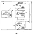
- Figure 1 of which is a block diagram illustrating the invention with its distributed program sequencing and de-coupled instruction data flow
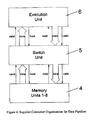
- Figure 4 is a suitable supplier-consumer organizational configuration for the data pipeline
- Figure 5 is a diagram of a preferred memory unit organization including two dual ported memory banks and two read-side and two write-side interfaces
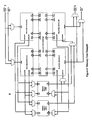
- Figure 6 is a combined circuit and block diagram that can be programmed with the lookup table of Figure 7
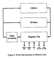
- Figure 8 is a diagram of the write-side interface useful with the invention
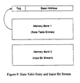
- Figure 9 illustrates the memory units operating as a finite state machine wherein two read-side interfaces are used in synchronization to read state table entries in one memory bank, and the input bid stream in the other.
- the instruction fetch and instruction decode stages are the central nerve system of the whole processor, and the efficiency of the entire processor is dependent on the translation of incoming instructions every clock cycle to control signals to drive all the hardware in the pipelines stages to perform useful work. This has to be done, moreover, with all the hardware, software and bandwidth constraints described above.
- the invention thus provides a flexible programming method, control mechanism and processor architecture in which the hardware resource in the processor P, preferably of pipelined architecture PS, is divided into functional blocks (e.g. Execution Units 6, Memory Units 4, and Switch Unit 5), for example, as described in said co-pending application.
- Each functional block has its own local program memory, labeled "program memory”, a sequencer, so-labeled, to fetch the instruction from the program memory, and to decode the instruction and to generate control vectors that will control the functionality of the hardware in the datapath, every clock cycle, as more completely shown in Figure 2 .
- Such an instruction set design allows the same instruction set to program diverse hardware blocks that require different numbers of bits for coding their respective control vectors.
- the calculation of the next instruction address depends on current instruction coding and a condition signal that is connected to the instruction sequencer, as in Figure 2 .
- the parent block control unit C initializes bulk transfer of programs (usually through DMA) and control vectors into their assigned memory space in the subsidiary or child blocks.
- the invention uses, in preferred implementation, a ring-type bus, Figure 3 , that starts and ends at the parent block, and that passes through each of its subsidiary blocks.
- This ring-type bus is used to pass messages between the control unit parent block and all of its subsidiary blocks 4, 5, 6, etc. through a general purpose register and memory read/write protocol. For example, it can be used by the control block C to set the program counter register to point to the beginning of the next module of the program to be executed in subsidiary blocks.
- an optional set of start signals from the parent control block C to subsidiary blocks may also be used to control the exact clock cycles that execution of certain program modules begin; and an optional set of interrupt signals from subsidiary blocks back to the parent block may also be provided to request attention from the parent control block.
- the subsidiary block can raise the signal to indicate that it has completed the execution of a program module.
- the method of mapping a target data processing program to instruction sequences for the above-mentioned processor design of the invention involves the following steps:
- the preferred Memory Unit design suitable for the programmable pipeline architecture of said co-pending patent application common hardware, structures are used to assist the fast execution of software algorithms and operations.
- the preferred processor design of the invention includes multiple Memory Units that can be programmed either to operate as independent data memory storage for different and independent computation blocks, or to operate in synchronization to provide for unified data memory storage with appropriate addressing modes (e.g. two-dimensional addressing, rotate addressing, etc.) for the interconnected computation blocks.
- appropriate addressing modes e.g. two-dimensional addressing, rotate addressing, etc.
- the datapth of a Memory Unit is shown including two dual-ported memory banks (labeled as "Bank 0" and "Bank 1") in Figures 5 and 6 , two Read Side Interfaces, two Write Side Interfaces, and a Data and Status Exchange (DSE) as labeled in Figure 6 .
- the two Read Side Interfaces have different functionality.
- the two Write Side Interfaces also have different functionality.
- the connections of which Write Side Interface to which memory bank, as well as which Read Side Interface to which memory bank, are programmable.
- the hardware allows the set up of hierarchical data pipelines.
- the DSE sets up data and status exchange between read interfaces and write interfaces of the two memory banks.
- each read interface or write interface sets up specific data pipeline for specific processing within the interface unit.
- the invention allows synchronized reads, synchronized writes, or synchronized read and write within the same memory banks or between two memory banks for different operations.
- the invention also enables the sending and receiving of data from the Switch Unit 5 to the appropriate memory banks as part of the data pipeline operation, and at the same time sending and receiving data from the DMA to the appropriate memory banks for bulk transfer of data to external memory. (In practice, this is intended to operate with the before-mentioned deterministic cache load and unload, to get ready for the next task or program module).
- the Read Side Interface of Figure 6 consists of an ALU, a data mask and selection block, and a small random access memory (RAM) that can be programmed with a lookup table, so-labeled in Figure 7 .
- the data mask and selection block can mask out certain bits in a data word or select sub-word in a data word to pass on.
- the RAM can be programmed with a lookup table in which an input address can be used to retrieve one line of content that is an address pointer for addressing the control vector memory for this functional unit.
- the RAM can be configured to accept address input from different sources (e.g. part of data being processed or status in the datapath).
- the Write Side Interface of Figure 6 is shown in Figure 8 consisting of an ALU and a data combiner block.
- the data combiner can merge two sub-words from two data words to form a new data word.
- the Read Side Interface and the Write Side Interface enable different modes of address computation for memory read and write. They also enable the processing of read data after a read operation and processing of write data before a write operation.
- FSM Finite State Machine
Landscapes
- Engineering & Computer Science (AREA)
- Software Systems (AREA)
- Theoretical Computer Science (AREA)
- Physics & Mathematics (AREA)
- General Engineering & Computer Science (AREA)
- General Physics & Mathematics (AREA)
- Advance Control (AREA)
- Executing Machine-Instructions (AREA)
- Complex Calculations (AREA)
Claims (37)
- Verfahren zur synchron getakteten, flexibel programmierbaren Datenverarbeitung mit einem Prozessor (P) aufweisend eine Vielzahl verschiedener Funktionseinheiten enthaltend Rechnereinheiten (6), Speichereinheiten (4), Schalteinheiten (5) zu deren Verbindung und zugehörige Steuereinheiten (C), wobei das Verfahren folgende Schritte umfasst:Verbinden verschiedener Funktionseinheiten (4, 5, 6) zur Bildung vorgegebener Steuerungspfade und Datenpipelines in einer hierarchischen Weise;Nutzen eines gemeinsamen Befehlssatzes zur Programmierung aller Funktionseinheiten (4, 5, 6), wobei der Befehlssatz direkt die Befehlsfolge codiert und direkt oder indirekt eine Hardware-Steuerung codiert;Erstellen verteilter Programmfolgen für jede Funktionseinheit (4, 5, 6) aufweisend einen eigenen Programmzähler, Befehlsabruf- und Dekodierungseinheiten und einen eigenen lokalen Speicher zur Programmspeicherung;Zugreifen auf die im Speicher gespeicherten Steuerungsvektoren zum Steuern der Datenpfade der Funktionseinheiten zu jeder Taktzeit; undKonfigurieren der Vielfach-Speichereinheiten (4) zum Betrieb in verschiedenen Speicherzugriffsmodi und Verbinden der Vielfach-Speichereinheiten (4) mit den funktionalen Rechnereinheiten (6) durch die Schalteinheiten (5).
- Verfahren nach Anspruch 1, wobei der Prozessor (P) zumindest teilweise durch ein in verschiedene Datenverarbeitungsmodule unterteiltes Datenverarbeitungsprogramm gesteuert wird, wobei jedes Datenverarbeitungsmodul durch eine von einer oder mehreren Funktionseinheiten (4, 5, 6) im Prozessor erzeugten Datenpipeline angesprochen wird und wobei jede Datenpipeline durch einzelne oder mehrere synchron getaktete Befehlsfolgen erzeugt wird, und zwar eine für jede Funktionseinheit (4, 5, 6) entlang der Datenpipeline.
- Verfahren nach Anspruch 2, wobei verschiedene Datenverarbeitungsmodule wie folgt abgebildet werden können; a: auf verschiedene Hardware-Blöcke mit Verbindungen zu den Blöcken, die für die Fortschaltung von einem zum nächsten Modul genutzt werden; b: auf denselben Hardwareblock unter Ausführung von Modulen, die zur Modulfortschaltung in unterschiedliche Zeitschlitze gemultiplext werden und c: eine Kombination aus a und b.
- Verfahren nach Anspruch 3, wobei die Steuerung und Synchronisation der Fortschaltung von einem Datenverarbeitungsmodul zum nächsten in Zeitschlitzen durch Befehlsfolgen in einer Stamm-Steuereinheit (C) für alle Funktionseinheiten (4, 5, 6) erfolgt, um die Datenpipeline zu erzeugen.
- Verfahren nach Anspruch 4, wobei die Hardware des Prozessors (P) dynamisch in einer oder mehreren Datenpipelines organisiert wird.
- Verfahren nach Anspruch 5, wobei jede Datenpipeline einer hierarchischen Struktur folgt, mit einem Datenfluss, der zuerst zwischen unterschiedlichen Stammeinheiten (C) etabliert wird und dann zwischen Untereinheiten der Stammeinheiten (4, 5, 6) etabliert wird, und zwar derart, dass die gesamte Datenpipeline von einer Ebene in die andere erzeugt wird.
- Verfahren nach Anspruch 1, wobei die Funktionseinheiten im Prozessor (P) dynamisch in einer Steuerungshierarchie organisiert werden, in der eine Stamm-Steuereinheit (C) bereitgestellt wird, die nur Steuerungs- und Synchronisationsmeldungen und -signale mit den entsprechenden Untereinheiten (4, 5, 6) austauscht.
- Verfahren nach Anspruch 1, wobei die Datenverarbeitung durch parallele Ausführung von Befehlsfolgen in heterogenen Hardware-Blöcken durchgeführt wird.
- Verfahren nach Anspruch 1, wobei die funktionalen Rechnereinheiten (6) flexibel angeordnet werden.
- Verfahren nach Anspruch 1, wobei derselbe Befehlssatz verwendet wird, um verschiedene funktionelle Hardware-Blöcke zu programmieren, die eine unterschiedliche Anzahl an Bits für ihre jeweilige Steuerungscodierung benötigen.
- Verfahren nach Anspruch 10, wobei der Befehlssatz ein Befehlsformat verwendet, welches eine direkte Codierung einer Befehlsfolge, eine direkte Codierung eines Tellsatzes der Hardware-Steuerungen und eine indirekte Codierung der Hardware-Steuerungen durch entweder einen Adresszeiger auf einen Steuerungsvektor-Speicher oder durch einen Lese- und Schreibbefehl auf ein Register erlaubt.
- Verfahren nach Anspruch 11, wobei die in einem Befehl codierten Hardware-Steuerungen die Organisation und Abhängigkeit der Unterblöcke innerhalb eines Blocks zur Bildung eines spezifischen Hardwarekonstruktes spezifizieren.
- Verfahren nach Anspruch 1, wobei jede der Speichereinheiten (4) zwei Speicherbanken mit zwei Eingängen enthält, wobei jede der Speicherbanken abwechselnd Teil eines Datenpipeline-Konstrukts sein kann und über Schnittstellen mit einem externen Speicher zum Laden und Entladen großer Datenmengen verbunden sein kann.
- Verfahren nach Anspruch 13, wobei jede der zwei Speicherbanken durch einen Befehl programmiert wird, sich mit einer von zwei ausleseseitigen Schnittstellen unterschiedlicher Funktionalität und einer von zwei schreibseitigen Schnittstellen unterschiedlicher Funktionalität zu verbinden.
- Verfahren nach Anspruch 14, wobei jede der vier Schnittstellen eine arithmetische Einheit aufweist, die eine Reihe von schnittstellenspezifischen und auf andere Elemente bezogene Funktionalitäten unterstützt, um verschiedene Arten einer Speicheradressberechnung oder eine einfache Datenverarbeitung zu ermöglichen.
- Verfahren nach Anspruch 14, wobei jede der Speichereinheiten (4) dafür genutzt wird, eine hierarchische Datenpipeline zu erzeugen, umfassend das Programmieren einer DSE zum Daten- und Status-Austausch zwischen den zwei ausleseseitigen Schnittstellen und den zwei schreibseitigen Schnittstellen, wobei die DSE die zwei Speicherbänke bei der notwendigen Koordination und zeitlichen Abgleichung unter den vier Schnittstellen unterstützt; und das Programmieren jeder der vier Schnittstellen, um eine Datenpipeline innerhalb der Schnittstelle zu etablieren, wobei die arithmetische Einheit für einfache Datenverarbeitung genutzt werden kann, bevor Daten auf die Speicherbank geschrieben werden oder nachdem Daten von der Speicherbank ausgelesen werden.
- Verfahren nach Anspruch 1, wobei ein endlicher Zustandsautomat implementiert wird, indem eine Speicherbank in den Speichereinheiten (4) zur Aufnahme von Statuseinträgen genutzt wird und eine Befehlsfolge für die Speichereinheit genutzt wird, an einer anderen Speicherbank die Eingangs-Daten-Bit-Ströme zu bearbeiten, um von einem Statuseintrag zum nächsten zu schreiten.
- Verfahren nach Anspruch 7, wobei ein Ringbus zwischen der Prozessor-Stamm-Steuereinheit (C) und den davon gesteuerten Funktionseinheiten, die Ausführeinheiten (6), Schalteinheiten (5) und Speichereinheiten (4) umfassen, verwendet wird.
- Synchron getakteter, flexibel programmierbarer Datenprozessor (P) umfassend eine Vielzahl verschiedener funktionaler Rechnereinheiten (6), Speichereinheiten (4), Vollzugriffs-Schalteinheiten (5) zu deren Verbindung und Steuereinheiten (C), wobei die Vorrichtung in Kombination aufweist
Verbindungen zwischen den verschiedenen Funktionseinheiten (4, 5, 6) zur Bildung vorgegebener Steuerungspfade und Datenpipelines in einer hierarchischen Weise;
einen gemeinsamen Befehlssatz zur Programmierung aller Funktionseinheiten (4, 5, 6), wobei der Befehlssatz direkt Befehlsfolgen codiert und direkt oder indirekt Hardware-Steuerungen codiert;
eine auf jede Funktionseinheit (4, 5, 6) verteilte Ablaufsteuerung mit eignem Programmzähler, Befehlsempfänger- und -dekodierungseinheiten und eigenem lokalen Speicher zur Programmspeicherung;
Mittel zum Zugriff auf gespeicherte Steuerungsvektoren, um die Datenpfade solcher Funktionseinheiten zu jeder Taktzeit zu steuern; und
Mittel zum Konfigurieren mehrerer Speichereinheiten, um in verschiedenen Speicherzugriffsmodi zu arbeiten und Mittel zu ihrer Verbindung mit den funktionellen Rechnereinheiten (6) durch die Schaltereinheit (5). - Vorrichtung nach Anspruch 19, wobei der Prozessor (P) zumindest teilweise durch ein in verschiedene Datenverarbeitungsmodule unterteiltes Datenverarbeitungsprogramm gesteuert ist, wobei jedes Datenverarbeitungsmodul durch eine mit einer oder mehreren der Funktionseinheiten (4, 5, 6) im Prozessor erzeugten Datenpipeline angesprochen wird, wobei jede Datenpipeline durch einzelne oder mehrere synchron getaktete Befehlsfolgen, und zwar eine für jede der Funktionseinheiten (4, 5, 6) erzeugt wird.
- Vorrichtung nach Anspruch 20, wobei verschiedene Datenverarbeitungsmodule auf verschiedene Hardware-Blöcke mit Verbindungen zwischen den Blöcken zur Fortschaltung von einem Modul zum nächsten abgebildet werden können.
- Vorrichtung nach Anspruch 20, wobei verschiedene Datenverarbeitungsmodule auf denselben Hardware-Block abgebildet sind, und zwar durch Ausführung von in unterschiedliche Zeitschlitze gemultiplexter Module zur Modulfortschreitung,
- Vorrichtung nach Anspruch 21 oder 22, wobei die Steuerung und Synchronisation der Fortschaltung von Daten von einem Datenverarbeitungsmodul zum nächsten in Zeitschlitzen durch Befehlsfolgen in der Stamm-Steuereinheit für alle Funktionseinheiten, die zur Erzeugung der Datenpipeline benutzt werden, erfolgt.
- Vorrichtung nach Anspruch 19, wobei die Hardware des Prozessors (P) in einer oder mehreren Datenpipelines dynamisch organisiert ist.
- Vorrichtung nach Anspruch 24, wobei jede Datenpipeline einer hierarchischen Struktur folgt, mit einem Datenfluss, der zuerst zwischen verschiedenen Stammeinheiten (C) und dann zwischen den Untereinheiten (4, 5, 6) einer Stammeinheit etabliert wird und zwar derart, dass die gesamte Datenpipeline von einer Ebene zur nächsten erzeugt wird.
- Vorrichtung nach Anspruch 19, wobei die Funktionseinheiten (4, 5, 6) im Prozessor (P) in einer Steuerungshierarchie dynamisch organisiert sind, in der jede Stamm-Steuereinheit (C) nur Steuerungs- und Synchronisierungsmeldungen und -signale mit ihren Untereinheiten austaucht.
- Vorrichtung nach Anspruch 19, wobei die Datenverarbeitung durch parallele Ausführung von Befehlsfolgen in heterogenen Hardware-Blöcken durchgeführt ist.
- Vorrichtung nach Anspruch 19, wobei die funktionellen Rechnereinheiten (6) flexibel angeordnet sind.
- Vorrichtung nach Anspruch 19, wobei dieselbe Befehlsfolge zur Programmierung von verschiedenen funktionellen Hardware-Blöcken benutzt ist, die unterschiedliche Anzahlen an Bits für ihre jeweilige Steuerungscodierung benötigen.
- Vorrichtung nach Anspruch 29, wobei der Befehlsatz ein Befehlsformat nutzt, welches die direkte Codierung von Befehlsfolgen, die direkte Codierung einer Auswahl von Hardware-Steuerungen und die indirekte Codierung von Hardware-Steuerungen durch entweder einen Adresszeiger auf einen Steuerungsvektor-Speicher oder durch einen Lese- und Schreibbefehl auf ein Register erlaubt.
- Vorrichtung nach Anspruch 30, wobei die in einem Befehl codierte Hardware-Steuerung die Organisation und die gegenseitige Verschaltung der Unterblöcke innerhalb eines Blocks spezifiziert um ein spezifisches Hardwarekonstrukt zu bilden.
- Vorrichtung nach Anspruch 19, wobei eine Speichereinheit (4) zwei Speicherbänke mit zwei Eingängen enthält, wobei die Speicherbanken abwechselnd Teil eines Datenpipeline-Konstrukts sein können und über Schnittstellen mit einem externen Speicher zum Laden und Entladen großer Datenmengen verbunden sein können.
- Vorrichtung nach Anspruch 32, wobei jede der zwei Speicherbanken programmiert sein kann durch den Befehl, sich mit einer der zwei ausleseseitigen Schnittstellen verschiedener Funktionalität oder mit einer der zwei schreibseitigen Schnittstellen mit verschiedener Funktionalität zu verbinden.
- Vorrichtung nach Anspruch 33, wobei jede der vier Schnittstellen eine arithmetische Einheit aufweist, die einen Satz schnittstellenspezifischer Funktionalitäten und andere Elemente unterstützt, um verschiedene Arten der Speicheradressberechnung oder eine einfache Datenverarbeitung zu ermöglichen.
- Vorrichtung nach Anspruch 19, wobei jede Speichereinheit (4) zur Konstruktion einer hierarchischen Datenpipeline vorgesehen ist, wobei die Vorrichtung umfasst:Mittel zum Programmieren eines DSE zum Daten- und Statusaustausch zwischen den zwei ausleseseitigen Schnittstellen und den zwei schreibseitigen Schnittstellen, um die zwei Speicherbänke bei der notwendigen Koordination und Taktabgleichung zwischen den Schnittstellen zu unterstützen; undMittel zum Programmieren jeder der zwei Schnittstellen, um eine Datenpipeline innerhalb der Schnittstellen zu etablieren, wobei die arithmetische Einheit für eine einfache Datenverarbeitung genutzt werden kann bevor die Daten auf die Speicherbank geschrieben werden oder nachdem die Daten aus der Speicherbank gelesen werden.
- Vorrichtung nach Anspruch 19, wobei ein endlicher Zustandsautomat implementiert ist, indem eine Speicherbank in einer Speichereinheit genutzt wird, die Statuseinträge festzuhalten und eine Befehlsfolge für die Speichereinheit genutzt wird, an einer anderen Speicherbank die Eingangs-Datenbit-Ströme zu bearbeiten, um von einem Statuseintrag zum nächsten zu schreiten.
- Vorrichtung nach Anspruch 19, wobei ein Ringbus zwischen der Prozessor-Stamm-Steuereinheit (C) und den davon gesteuerten Funktionseinheiten umfassend Ausführeinheiten (6), Schalteinheiten (5) und Speichereinheiten (4) vorgesehen ist.
Applications Claiming Priority (2)
| Application Number | Priority Date | Filing Date | Title |
|---|---|---|---|
| US12/156,007 US8181003B2 (en) | 2008-05-29 | 2008-05-29 | Instruction set design, control and communication in programmable microprocessor cores and the like |
| PCT/IB2009/000131 WO2009144538A1 (en) | 2008-05-29 | 2009-01-26 | Method & apparatus for real-time data processing |
Publications (2)
| Publication Number | Publication Date |
|---|---|
| EP2289003A1 EP2289003A1 (de) | 2011-03-02 |
| EP2289003B1 true EP2289003B1 (de) | 2013-05-22 |
Family
ID=40668367
Family Applications (1)
| Application Number | Title | Priority Date | Filing Date |
|---|---|---|---|
| EP09754166.8A Not-in-force EP2289003B1 (de) | 2008-05-29 | 2009-01-26 | Verfahren und vorrichtung zur echtzeit-datenverarbeitung |
Country Status (8)
| Country | Link |
|---|---|
| US (1) | US8181003B2 (de) |
| EP (1) | EP2289003B1 (de) |
| JP (1) | JP2011525008A (de) |
| CN (1) | CN102144225A (de) |
| AU (1) | AU2009252885A1 (de) |
| CA (1) | CA2725130A1 (de) |
| TW (1) | TW200951809A (de) |
| WO (1) | WO2009144538A1 (de) |
Families Citing this family (40)
| Publication number | Priority date | Publication date | Assignee | Title |
|---|---|---|---|---|
| US7840914B1 (en) * | 2005-05-13 | 2010-11-23 | Massachusetts Institute Of Technology | Distributing computations in a parallel processing environment |
| TWI424371B (zh) * | 2009-12-30 | 2014-01-21 | Altek Corp | Video processing device and processing method thereof |
| CN102183921B (zh) * | 2011-03-01 | 2012-09-12 | 上海维宏电子科技股份有限公司 | 数控系统中实现限位自动释放功能的方法 |
| WO2012124995A2 (en) * | 2011-03-15 | 2012-09-20 | Samsung Electronics Co., Ltd. | Method and system for maintaining vector clocks during synchronization for data race detection |
| CN102508643A (zh) * | 2011-11-16 | 2012-06-20 | 刘大可 | 一种多核并行数字信号处理器及并行指令集的运行方法 |
| CN102393657B (zh) * | 2011-11-30 | 2014-11-05 | 洛阳正扬冶金技术股份有限公司 | 一种自动化控制系统的功能块化控制方法 |
| US8739101B1 (en) * | 2012-11-21 | 2014-05-27 | Maxeler Technologies Ltd. | Systems and methods for reducing logic switching noise in parallel pipelined hardware |
| JP5977209B2 (ja) * | 2013-07-18 | 2016-08-24 | 日本電信電話株式会社 | ステートマシン回路 |
| US20150178078A1 (en) * | 2013-12-21 | 2015-06-25 | H. Peter Anvin | Instructions and logic to provide base register swap status verification functionality |
| US9612840B2 (en) | 2014-03-28 | 2017-04-04 | Intel Corporation | Method and apparatus for implementing a dynamic out-of-order processor pipeline |
| US9582282B2 (en) * | 2014-07-17 | 2017-02-28 | Arm Limited | Prefetching using a prefetch lookup table identifying previously accessed cache lines |
| US20170177542A1 (en) * | 2015-12-16 | 2017-06-22 | Cognitive Systems Corp. | Operating a VLIW Processor in a Wireless Sensor Device |
| US10726034B2 (en) * | 2016-03-30 | 2020-07-28 | Microsoft Technology Licensing, Llc | Modular electronic data analysis computing system |
| CN106155632A (zh) * | 2016-08-02 | 2016-11-23 | 合肥奇也信息科技有限公司 | 一种用于计算机最优定位数据处理中小码集的系统 |
| CN112148753B (zh) * | 2016-08-26 | 2024-01-16 | 华为云计算技术有限公司 | 用于对数据流执行信息处理的设备和方法 |
| DE102017200456A1 (de) * | 2017-01-12 | 2018-07-12 | Robert Bosch Gmbh | Recheneinheit und Betriebsverfahren hierfür |
| US11853244B2 (en) * | 2017-01-26 | 2023-12-26 | Wisconsin Alumni Research Foundation | Reconfigurable computer accelerator providing stream processor and dataflow processor |
| US11132599B2 (en) | 2017-02-28 | 2021-09-28 | Microsoft Technology Licensing, Llc | Multi-function unit for programmable hardware nodes for neural network processing |
| US10956360B2 (en) * | 2017-03-14 | 2021-03-23 | Azurengine Technologies Zhuhai Inc. | Static shared memory access with one piece of input data to be reused for successive execution of one instruction in a reconfigurable parallel processor |
| US11151077B2 (en) | 2017-06-28 | 2021-10-19 | Wisconsin Alumni Research Foundation | Computer architecture with fixed program dataflow elements and stream processor |
| CN107729989B (zh) * | 2017-07-20 | 2020-12-29 | 安徽寒武纪信息科技有限公司 | 一种用于执行人工神经网络正向运算的装置及方法 |
| GB201717295D0 (en) * | 2017-10-20 | 2017-12-06 | Graphcore Ltd | Synchronization in a multi-tile processing array |
| KR102465213B1 (ko) * | 2018-03-31 | 2022-11-10 | 마이크론 테크놀로지, 인크. | 멀티 스레드, 자체 스케줄링 재구성 가능한 컴퓨팅 패브릭에 대한 조건부 브랜칭 제어 |
| CN108874730B (zh) * | 2018-06-14 | 2021-06-22 | 北京理工大学 | 一种数据处理器及数据处理方法 |
| CN110647358B (zh) * | 2018-06-27 | 2021-11-23 | 展讯通信(上海)有限公司 | 同步多线程处理器 |
| CN110647357B (zh) * | 2018-06-27 | 2021-12-03 | 展讯通信(上海)有限公司 | 同步多线程处理器 |
| EP3611722B1 (de) * | 2018-08-13 | 2024-09-25 | Axis AB | Steuergerät und verfahren zur reduzierung der spitzenleistungsaufnahme einer videobildverarbeitungspipeline |
| GB2577738B (en) * | 2018-10-05 | 2021-02-24 | Advanced Risc Mach Ltd | An apparatus and method for providing decoded instructions |
| CN111090464B (zh) * | 2018-10-23 | 2023-09-22 | 华为技术有限公司 | 一种数据流处理方法及相关设备 |
| CN110058882B (zh) * | 2019-03-14 | 2023-01-06 | 深圳市比昂芯科技有限公司 | 一种用于cnn加速的opu指令集定义方法 |
| WO2020197964A1 (en) | 2019-03-26 | 2020-10-01 | Axis Semiconductor, Inc. | Computing device with circuit switched memory access |
| KR102670905B1 (ko) * | 2019-08-22 | 2024-05-31 | 구글 엘엘씨 | 전파 지연 감소 |
| CN111475205B (zh) * | 2020-03-02 | 2023-03-17 | 上海交通大学 | 一种基于数据流解耦合的粗粒度可重构阵列结构设计方法 |
| CN112463723A (zh) * | 2020-12-17 | 2021-03-09 | 王志平 | 一种微内核阵列的实现方法 |
| CN113342269A (zh) * | 2021-05-31 | 2021-09-03 | 上海蓝色帛缔智能工程有限公司 | 基于云统计的多路数据存储的方法、装置、设备及介质 |
| CA3241053A1 (en) * | 2022-03-01 | 2023-09-07 | Rei Honma | Core design apparatus, core design method, and program |
| CN114883301B (zh) * | 2022-04-29 | 2023-03-21 | 西安电子科技大学 | 基于Chiplet的微系统可重构网络拓扑结构及实现方法 |
| CN115328551A (zh) * | 2022-08-01 | 2022-11-11 | 中国人民解放军国防科技大学 | 一种基于算子的微处理器架构设计方法及系统 |
| CN117111857B (zh) * | 2023-09-15 | 2024-05-07 | 上海合芯数字科技有限公司 | 读取数据信息的方法、装置、设备及存储介质 |
| CN118349286B (zh) * | 2024-06-18 | 2024-09-10 | 联芸科技(杭州)股份有限公司 | 处理器、指令处理的装置、电子设备以及指令处理方法 |
Family Cites Families (55)
| Publication number | Priority date | Publication date | Assignee | Title |
|---|---|---|---|---|
| JP3137117B2 (ja) * | 1987-03-27 | 2001-02-19 | 将容 曽和 | 高速処理計算機 |
| US5239654A (en) * | 1989-11-17 | 1993-08-24 | Texas Instruments Incorporated | Dual mode SIMD/MIMD processor providing reuse of MIMD instruction memories as data memories when operating in SIMD mode |
| US6070003A (en) * | 1989-11-17 | 2000-05-30 | Texas Instruments Incorporated | System and method of memory access in apparatus having plural processors and plural memories |
| US5212777A (en) * | 1989-11-17 | 1993-05-18 | Texas Instruments Incorporated | Multi-processor reconfigurable in single instruction multiple data (SIMD) and multiple instruction multiple data (MIMD) modes and method of operation |
| EP0429733B1 (de) * | 1989-11-17 | 1999-04-28 | Texas Instruments Incorporated | Multiprozessor mit Koordinatenschalter zwischen Prozessoren und Speichern |
| US5226125A (en) * | 1989-11-17 | 1993-07-06 | Keith Balmer | Switch matrix having integrated crosspoint logic and method of operation |
| US5471626A (en) * | 1992-05-06 | 1995-11-28 | International Business Machines Corporation | Variable stage entry/exit instruction pipeline |
| JP3546437B2 (ja) * | 1993-03-31 | 2004-07-28 | ソニー株式会社 | 適応形ビデオ信号演算処理装置 |
| US5706459A (en) | 1994-01-06 | 1998-01-06 | Fujitsu Limited | Processor having a variable number of stages in a pipeline |
| JP3251421B2 (ja) * | 1994-04-11 | 2002-01-28 | 株式会社日立製作所 | 半導体集積回路 |
| US6052773A (en) | 1995-02-10 | 2000-04-18 | Massachusetts Institute Of Technology | DPGA-coupled microprocessors |
| US5996083A (en) * | 1995-08-11 | 1999-11-30 | Hewlett-Packard Company | Microprocessor having software controllable power consumption |
| US5771362A (en) | 1996-05-17 | 1998-06-23 | Advanced Micro Devices, Inc. | Processor having a bus interconnect which is dynamically reconfigurable in response to an instruction field |
| US5784636A (en) | 1996-05-28 | 1998-07-21 | National Semiconductor Corporation | Reconfigurable computer architecture for use in signal processing applications |
| US5937203A (en) | 1996-09-16 | 1999-08-10 | Advanced Micro Devices, Inc. | Port for fine tuning a central processing unit |
| US5887160A (en) | 1996-12-10 | 1999-03-23 | Fujitsu Limited | Method and apparatus for communicating integer and floating point data over a shared data path in a single instruction pipeline processor |
| US6542998B1 (en) | 1997-02-08 | 2003-04-01 | Pact Gmbh | Method of self-synchronization of configurable elements of a programmable module |
| US6085317A (en) | 1997-08-15 | 2000-07-04 | Altera Corporation | Reconfigurable computer architecture using programmable logic devices |
| US6023753A (en) * | 1997-06-30 | 2000-02-08 | Billion Of Operations Per Second, Inc. | Manifold array processor |
| JP4156794B2 (ja) * | 1997-11-07 | 2008-09-24 | アルテラ コーポレイション | iVLIWのPE間通信を用いた効率的な同期MIMD動作のための方法および装置 |
| US6173389B1 (en) * | 1997-12-04 | 2001-01-09 | Billions Of Operations Per Second, Inc. | Methods and apparatus for dynamic very long instruction word sub-instruction selection for execution time parallelism in an indirect very long instruction word processor |
| US6101592A (en) * | 1998-12-18 | 2000-08-08 | Billions Of Operations Per Second, Inc. | Methods and apparatus for scalable instruction set architecture with dynamic compact instructions |
| US6216223B1 (en) * | 1998-01-12 | 2001-04-10 | Billions Of Operations Per Second, Inc. | Methods and apparatus to dynamically reconfigure the instruction pipeline of an indirect very long instruction word scalable processor |
| US6539438B1 (en) | 1999-01-15 | 2003-03-25 | Quickflex Inc. | Reconfigurable computing system and method and apparatus employing same |
| JP2001169068A (ja) * | 1999-12-14 | 2001-06-22 | Ricoh Co Ltd | 画像処理装置、画像処理方法およびその方法をコンピュータに実行させるプログラムを記録したコンピュータ読み取り可能な記録媒体 |
| US6704857B2 (en) * | 1999-12-23 | 2004-03-09 | Pts Corporation | Methods and apparatus for loading a very long instruction word memory |
| JP3922859B2 (ja) * | 1999-12-28 | 2007-05-30 | 株式会社リコー | 画像処理装置、画像処理方法およびその方法をコンピュータに実行させるプログラムを記録したコンピュータ読み取り可能な記録媒体 |
| EP1199629A1 (de) | 2000-10-17 | 2002-04-24 | STMicroelectronics S.r.l. | Prozessorarchitektur mit veränderlichen Pipelinestufen |
| GB2370380B (en) | 2000-12-19 | 2003-12-31 | Picochip Designs Ltd | Processor architecture |
| GB2370381B (en) | 2000-12-19 | 2003-12-24 | Picochip Designs Ltd | Processor architecture |
| US6574764B2 (en) | 2001-04-25 | 2003-06-03 | Agilent Technologies, Inc. | Algorithmically programmable memory tester with history FIFO's that aid in error analysis and recovery |
| US20030088757A1 (en) * | 2001-05-02 | 2003-05-08 | Joshua Lindner | Efficient high performance data operation element for use in a reconfigurable logic environment |
| US6859873B2 (en) | 2001-06-08 | 2005-02-22 | Infineon Technologies Ag | Variable length instruction pipeline |
| US20030043848A1 (en) * | 2001-08-30 | 2003-03-06 | Sonksen Bradley Stephen | Method and apparatus for data item processing control |
| US7200735B2 (en) | 2002-04-10 | 2007-04-03 | Tensilica, Inc. | High-performance hybrid processor with configurable execution units |
| DE60219152D1 (de) * | 2002-07-19 | 2007-05-10 | St Microelectronics Srl | Eine mehrphasige synchrone Pipelinestruktur |
| AU2003254126A1 (en) | 2002-07-23 | 2004-02-09 | Gatechance Technologies Inc | Pipelined reconfigurable dynamic instruciton set processor |
| US7571303B2 (en) | 2002-10-16 | 2009-08-04 | Akya (Holdings) Limited | Reconfigurable integrated circuit |
| KR100546331B1 (ko) * | 2003-06-03 | 2006-01-26 | 삼성전자주식회사 | 스택 뱅크들 마다 독립적으로 동작하는 멀티 포트 메모리장치 |
| TW200504592A (en) | 2003-07-24 | 2005-02-01 | Ind Tech Res Inst | Reconfigurable apparatus with high hardware efficiency |
| US8719837B2 (en) * | 2004-05-19 | 2014-05-06 | Synopsys, Inc. | Microprocessor architecture having extendible logic |
| JP2006018412A (ja) * | 2004-06-30 | 2006-01-19 | Fujitsu Ltd | アドレス生成器および演算回路 |
| JP4594666B2 (ja) * | 2004-07-12 | 2010-12-08 | 富士通株式会社 | 再構成可能な演算装置 |
| JP4201816B2 (ja) | 2004-07-30 | 2008-12-24 | 富士通株式会社 | リコンフィギュラブル回路およびリコンフィギュラブル回路の制御方法 |
| US7205864B2 (en) | 2004-11-02 | 2007-04-17 | Nextg Networks, Inc. | Distributed matrix switch |
| US7395411B2 (en) | 2005-03-14 | 2008-07-01 | Sony Computer Entertainment Inc. | Methods and apparatus for improving processing performance by controlling latch points |
| JP4527571B2 (ja) * | 2005-03-14 | 2010-08-18 | 富士通株式会社 | 再構成可能演算処理装置 |
| US8966223B2 (en) | 2005-05-05 | 2015-02-24 | Icera, Inc. | Apparatus and method for configurable processing |
| TWI259659B (en) | 2005-05-13 | 2006-08-01 | Ind Tech Res Inst | Pipelined datapath with dynamically reconfigurable pipeline stages |
| US7454598B2 (en) | 2005-05-16 | 2008-11-18 | Infineon Technologies Ag | Controlling out of order execution pipelines issue tagging |
| US20060259742A1 (en) | 2005-05-16 | 2006-11-16 | Infineon Technologies North America Corp. | Controlling out of order execution pipelines using pipeline skew parameters |
| JP4861030B2 (ja) * | 2006-03-24 | 2012-01-25 | 株式会社東芝 | 半導体装置 |
| US8099583B2 (en) | 2006-08-23 | 2012-01-17 | Axis Semiconductor, Inc. | Method of and apparatus and architecture for real time signal processing by switch-controlled programmable processor configuring and flexible pipeline and parallel processing |
| US7519797B1 (en) * | 2006-11-02 | 2009-04-14 | Nividia Corporation | Hierarchical multi-precision pipeline counters |
| US8078833B2 (en) * | 2008-05-29 | 2011-12-13 | Axis Semiconductor, Inc. | Microprocessor with highly configurable pipeline and executional unit internal hierarchal structures, optimizable for different types of computational functions |
-
2008
- 2008-05-29 US US12/156,007 patent/US8181003B2/en active Active
-
2009
- 2009-01-26 CA CA2725130A patent/CA2725130A1/en not_active Abandoned
- 2009-01-26 EP EP09754166.8A patent/EP2289003B1/de not_active Not-in-force
- 2009-01-26 JP JP2011511099A patent/JP2011525008A/ja active Pending
- 2009-01-26 WO PCT/IB2009/000131 patent/WO2009144538A1/en not_active Ceased
- 2009-01-26 CN CN2009801307349A patent/CN102144225A/zh active Pending
- 2009-01-26 AU AU2009252885A patent/AU2009252885A1/en not_active Abandoned
- 2009-02-10 TW TW098104221A patent/TW200951809A/zh unknown
Also Published As
| Publication number | Publication date |
|---|---|
| JP2011525008A (ja) | 2011-09-08 |
| EP2289003A1 (de) | 2011-03-02 |
| US8181003B2 (en) | 2012-05-15 |
| CN102144225A (zh) | 2011-08-03 |
| CA2725130A1 (en) | 2009-12-03 |
| AU2009252885A1 (en) | 2009-12-03 |
| WO2009144538A1 (en) | 2009-12-03 |
| US20090300337A1 (en) | 2009-12-03 |
| TW200951809A (en) | 2009-12-16 |
Similar Documents
| Publication | Publication Date | Title |
|---|---|---|
| EP2289003B1 (de) | Verfahren und vorrichtung zur echtzeit-datenverarbeitung | |
| KR100236525B1 (ko) | 넓은 데이타 폭의 프로세서에서 다기능 데이타 정렬기 | |
| KR0178078B1 (ko) | 2개의 명령이 동시 실행 가능한 데이타 프로세서 | |
| US9021236B2 (en) | Methods and apparatus for storing expanded width instructions in a VLIW memory for deferred execution | |
| GB2287109A (en) | Multiple execution unit bypasses for efficient processor execution | |
| US7383419B2 (en) | Address generation unit for a processor | |
| US7139899B2 (en) | Selected register decode values for pipeline stage register addressing | |
| CN100380315C (zh) | 提供多指令集和多译码模式的设备和方法 | |
| JP3866513B2 (ja) | データストリーミングのためのコンピュータのプロセッサ及び方法 | |
| US11726912B2 (en) | Coupling wide memory interface to wide write back paths | |
| US7143268B2 (en) | Circuit and method for instruction compression and dispersal in wide-issue processors | |
| US6442675B1 (en) | Compressed string and multiple generation engine | |
| US8631173B2 (en) | Semiconductor device | |
| US7028164B2 (en) | Instruction fetch apparatus for wide issue processors and method of operation | |
| US20020083306A1 (en) | Digital signal processing apparatus | |
| HK1160530A (en) | Method & apparatus for real-time data processing | |
| CN121658075A (zh) | 一种基于risc-v指令集架构的32位处理器 | |
| JPH10260832A (ja) | 情報処理装置 | |
| JP2004326710A (ja) | 演算処理装置及び方法 |
Legal Events
| Date | Code | Title | Description |
|---|---|---|---|
| PUAI | Public reference made under article 153(3) epc to a published international application that has entered the european phase |
Free format text: ORIGINAL CODE: 0009012 |
|
| 17P | Request for examination filed |
Effective date: 20101223 |
|
| AK | Designated contracting states |
Kind code of ref document: A1 Designated state(s): AT BE BG CH CY CZ DE DK EE ES FI FR GB GR HR HU IE IS IT LI LT LU LV MC MK MT NL NO PL PT RO SE SI SK TR |
|
| AX | Request for extension of the european patent |
Extension state: AL BA RS |
|
| RIN1 | Information on inventor provided before grant (corrected) |
Inventor name: PITARYS, GREGORY Inventor name: NING, KE Inventor name: WU, QIAN Inventor name: WANG, FUGUI Inventor name: MARSHALL, BENJAMIN Inventor name: WANG, XIAOLIN |
|
| DAX | Request for extension of the european patent (deleted) | ||
| 17Q | First examination report despatched |
Effective date: 20110819 |
|
| GRAP | Despatch of communication of intention to grant a patent |
Free format text: ORIGINAL CODE: EPIDOSNIGR1 |
|
| RIN1 | Information on inventor provided before grant (corrected) |
Inventor name: WU, QIAN Inventor name: WANG, XIAOLIN Inventor name: NING, KE Inventor name: WANG, FUGUI Inventor name: PITARYS, GREGORY Inventor name: MARSHALL, BENJAMIN |
|
| GRAS | Grant fee paid |
Free format text: ORIGINAL CODE: EPIDOSNIGR3 |
|
| GRAA | (expected) grant |
Free format text: ORIGINAL CODE: 0009210 |
|
| AK | Designated contracting states |
Kind code of ref document: B1 Designated state(s): AT BE BG CH CY CZ DE DK EE ES FI FR GB GR HR HU IE IS IT LI LT LU LV MC MK MT NL NO PL PT RO SE SI SK TR |
|
| REG | Reference to a national code |
Ref country code: GB Ref legal event code: FG4D |
|
| REG | Reference to a national code |
Ref country code: CH Ref legal event code: EP |
|
| REG | Reference to a national code |
Ref country code: AT Ref legal event code: REF Ref document number: 613562 Country of ref document: AT Kind code of ref document: T Effective date: 20130615 |
|
| REG | Reference to a national code |
Ref country code: IE Ref legal event code: FG4D |
|
| REG | Reference to a national code |
Ref country code: DE Ref legal event code: R096 Ref document number: 602009015917 Country of ref document: DE Effective date: 20130718 |
|
| REG | Reference to a national code |
Ref country code: SE Ref legal event code: TRGR |
|
| REG | Reference to a national code |
Ref country code: NL Ref legal event code: T3 |
|
| REG | Reference to a national code |
Ref country code: AT Ref legal event code: MK05 Ref document number: 613562 Country of ref document: AT Kind code of ref document: T Effective date: 20130522 |
|
| REG | Reference to a national code |
Ref country code: LT Ref legal event code: MG4D |
|
| PG25 | Lapsed in a contracting state [announced via postgrant information from national office to epo] |
Ref country code: NO Free format text: LAPSE BECAUSE OF FAILURE TO SUBMIT A TRANSLATION OF THE DESCRIPTION OR TO PAY THE FEE WITHIN THE PRESCRIBED TIME-LIMIT Effective date: 20130822 Ref country code: PT Free format text: LAPSE BECAUSE OF FAILURE TO SUBMIT A TRANSLATION OF THE DESCRIPTION OR TO PAY THE FEE WITHIN THE PRESCRIBED TIME-LIMIT Effective date: 20130923 Ref country code: ES Free format text: LAPSE BECAUSE OF FAILURE TO SUBMIT A TRANSLATION OF THE DESCRIPTION OR TO PAY THE FEE WITHIN THE PRESCRIBED TIME-LIMIT Effective date: 20130902 Ref country code: LT Free format text: LAPSE BECAUSE OF FAILURE TO SUBMIT A TRANSLATION OF THE DESCRIPTION OR TO PAY THE FEE WITHIN THE PRESCRIBED TIME-LIMIT Effective date: 20130522 Ref country code: FI Free format text: LAPSE BECAUSE OF FAILURE TO SUBMIT A TRANSLATION OF THE DESCRIPTION OR TO PAY THE FEE WITHIN THE PRESCRIBED TIME-LIMIT Effective date: 20130522 Ref country code: GR Free format text: LAPSE BECAUSE OF FAILURE TO SUBMIT A TRANSLATION OF THE DESCRIPTION OR TO PAY THE FEE WITHIN THE PRESCRIBED TIME-LIMIT Effective date: 20130823 Ref country code: AT Free format text: LAPSE BECAUSE OF FAILURE TO SUBMIT A TRANSLATION OF THE DESCRIPTION OR TO PAY THE FEE WITHIN THE PRESCRIBED TIME-LIMIT Effective date: 20130522 Ref country code: IS Free format text: LAPSE BECAUSE OF FAILURE TO SUBMIT A TRANSLATION OF THE DESCRIPTION OR TO PAY THE FEE WITHIN THE PRESCRIBED TIME-LIMIT Effective date: 20130922 Ref country code: SI Free format text: LAPSE BECAUSE OF FAILURE TO SUBMIT A TRANSLATION OF THE DESCRIPTION OR TO PAY THE FEE WITHIN THE PRESCRIBED TIME-LIMIT Effective date: 20130522 |
|
| PG25 | Lapsed in a contracting state [announced via postgrant information from national office to epo] |
Ref country code: BG Free format text: LAPSE BECAUSE OF FAILURE TO SUBMIT A TRANSLATION OF THE DESCRIPTION OR TO PAY THE FEE WITHIN THE PRESCRIBED TIME-LIMIT Effective date: 20130822 Ref country code: HR Free format text: LAPSE BECAUSE OF FAILURE TO SUBMIT A TRANSLATION OF THE DESCRIPTION OR TO PAY THE FEE WITHIN THE PRESCRIBED TIME-LIMIT Effective date: 20130522 Ref country code: PL Free format text: LAPSE BECAUSE OF FAILURE TO SUBMIT A TRANSLATION OF THE DESCRIPTION OR TO PAY THE FEE WITHIN THE PRESCRIBED TIME-LIMIT Effective date: 20130522 |
|
| PG25 | Lapsed in a contracting state [announced via postgrant information from national office to epo] |
Ref country code: LV Free format text: LAPSE BECAUSE OF FAILURE TO SUBMIT A TRANSLATION OF THE DESCRIPTION OR TO PAY THE FEE WITHIN THE PRESCRIBED TIME-LIMIT Effective date: 20130522 |
|
| PG25 | Lapsed in a contracting state [announced via postgrant information from national office to epo] |
Ref country code: SK Free format text: LAPSE BECAUSE OF FAILURE TO SUBMIT A TRANSLATION OF THE DESCRIPTION OR TO PAY THE FEE WITHIN THE PRESCRIBED TIME-LIMIT Effective date: 20130522 Ref country code: BE Free format text: LAPSE BECAUSE OF FAILURE TO SUBMIT A TRANSLATION OF THE DESCRIPTION OR TO PAY THE FEE WITHIN THE PRESCRIBED TIME-LIMIT Effective date: 20130522 Ref country code: CZ Free format text: LAPSE BECAUSE OF FAILURE TO SUBMIT A TRANSLATION OF THE DESCRIPTION OR TO PAY THE FEE WITHIN THE PRESCRIBED TIME-LIMIT Effective date: 20130522 Ref country code: EE Free format text: LAPSE BECAUSE OF FAILURE TO SUBMIT A TRANSLATION OF THE DESCRIPTION OR TO PAY THE FEE WITHIN THE PRESCRIBED TIME-LIMIT Effective date: 20130522 Ref country code: DK Free format text: LAPSE BECAUSE OF FAILURE TO SUBMIT A TRANSLATION OF THE DESCRIPTION OR TO PAY THE FEE WITHIN THE PRESCRIBED TIME-LIMIT Effective date: 20130522 |
|
| PG25 | Lapsed in a contracting state [announced via postgrant information from national office to epo] |
Ref country code: RO Free format text: LAPSE BECAUSE OF FAILURE TO SUBMIT A TRANSLATION OF THE DESCRIPTION OR TO PAY THE FEE WITHIN THE PRESCRIBED TIME-LIMIT Effective date: 20130522 |
|
| PLBE | No opposition filed within time limit |
Free format text: ORIGINAL CODE: 0009261 |
|
| STAA | Information on the status of an ep patent application or granted ep patent |
Free format text: STATUS: NO OPPOSITION FILED WITHIN TIME LIMIT |
|
| 26N | No opposition filed |
Effective date: 20140225 |
|
| REG | Reference to a national code |
Ref country code: DE Ref legal event code: R097 Ref document number: 602009015917 Country of ref document: DE Effective date: 20140225 |
|
| REG | Reference to a national code |
Ref country code: DE Ref legal event code: R119 Ref document number: 602009015917 Country of ref document: DE |
|
| REG | Reference to a national code |
Ref country code: NL Ref legal event code: V1 Effective date: 20140801 |
|
| PG25 | Lapsed in a contracting state [announced via postgrant information from national office to epo] |
Ref country code: MC Free format text: LAPSE BECAUSE OF FAILURE TO SUBMIT A TRANSLATION OF THE DESCRIPTION OR TO PAY THE FEE WITHIN THE PRESCRIBED TIME-LIMIT Effective date: 20130522 Ref country code: LU Free format text: LAPSE BECAUSE OF FAILURE TO SUBMIT A TRANSLATION OF THE DESCRIPTION OR TO PAY THE FEE WITHIN THE PRESCRIBED TIME-LIMIT Effective date: 20140126 |
|
| REG | Reference to a national code |
Ref country code: CH Ref legal event code: PL |
|
| REG | Reference to a national code |
Ref country code: SE Ref legal event code: EUG |
|
| GBPC | Gb: european patent ceased through non-payment of renewal fee |
Effective date: 20140126 |
|
| REG | Reference to a national code |
Ref country code: DE Ref legal event code: R119 Ref document number: 602009015917 Country of ref document: DE Effective date: 20140801 |
|
| PG25 | Lapsed in a contracting state [announced via postgrant information from national office to epo] |
Ref country code: DE Free format text: LAPSE BECAUSE OF NON-PAYMENT OF DUE FEES Effective date: 20140801 Ref country code: LI Free format text: LAPSE BECAUSE OF NON-PAYMENT OF DUE FEES Effective date: 20140131 Ref country code: NL Free format text: LAPSE BECAUSE OF NON-PAYMENT OF DUE FEES Effective date: 20140801 Ref country code: CH Free format text: LAPSE BECAUSE OF NON-PAYMENT OF DUE FEES Effective date: 20140131 |
|
| REG | Reference to a national code |
Ref country code: FR Ref legal event code: ST Effective date: 20140930 |
|
| REG | Reference to a national code |
Ref country code: IE Ref legal event code: MM4A |
|
| PG25 | Lapsed in a contracting state [announced via postgrant information from national office to epo] |
Ref country code: GB Free format text: LAPSE BECAUSE OF NON-PAYMENT OF DUE FEES Effective date: 20140126 Ref country code: FR Free format text: LAPSE BECAUSE OF NON-PAYMENT OF DUE FEES Effective date: 20140131 Ref country code: SE Free format text: LAPSE BECAUSE OF NON-PAYMENT OF DUE FEES Effective date: 20140127 |
|
| PG25 | Lapsed in a contracting state [announced via postgrant information from national office to epo] |
Ref country code: IE Free format text: LAPSE BECAUSE OF NON-PAYMENT OF DUE FEES Effective date: 20140126 |
|
| PG25 | Lapsed in a contracting state [announced via postgrant information from national office to epo] |
Ref country code: MT Free format text: LAPSE BECAUSE OF FAILURE TO SUBMIT A TRANSLATION OF THE DESCRIPTION OR TO PAY THE FEE WITHIN THE PRESCRIBED TIME-LIMIT Effective date: 20130522 |
|
| PG25 | Lapsed in a contracting state [announced via postgrant information from national office to epo] |
Ref country code: IT Free format text: LAPSE BECAUSE OF NON-PAYMENT OF DUE FEES Effective date: 20140126 Ref country code: CY Free format text: LAPSE BECAUSE OF FAILURE TO SUBMIT A TRANSLATION OF THE DESCRIPTION OR TO PAY THE FEE WITHIN THE PRESCRIBED TIME-LIMIT Effective date: 20130522 |
|
| PG25 | Lapsed in a contracting state [announced via postgrant information from national office to epo] |
Ref country code: TR Free format text: LAPSE BECAUSE OF FAILURE TO SUBMIT A TRANSLATION OF THE DESCRIPTION OR TO PAY THE FEE WITHIN THE PRESCRIBED TIME-LIMIT Effective date: 20130522 Ref country code: HU Free format text: LAPSE BECAUSE OF FAILURE TO SUBMIT A TRANSLATION OF THE DESCRIPTION OR TO PAY THE FEE WITHIN THE PRESCRIBED TIME-LIMIT; INVALID AB INITIO Effective date: 20090126 |
|
| PG25 | Lapsed in a contracting state [announced via postgrant information from national office to epo] |
Ref country code: MK Free format text: LAPSE BECAUSE OF FAILURE TO SUBMIT A TRANSLATION OF THE DESCRIPTION OR TO PAY THE FEE WITHIN THE PRESCRIBED TIME-LIMIT Effective date: 20130522 |