EP2282606B1 - Procédé de commande pour un appareil à induction et appareil à induction - Google Patents
Procédé de commande pour un appareil à induction et appareil à induction Download PDFInfo
- Publication number
- EP2282606B1 EP2282606B1 EP09380143A EP09380143A EP2282606B1 EP 2282606 B1 EP2282606 B1 EP 2282606B1 EP 09380143 A EP09380143 A EP 09380143A EP 09380143 A EP09380143 A EP 09380143A EP 2282606 B1 EP2282606 B1 EP 2282606B1
- Authority
- EP
- European Patent Office
- Prior art keywords
- switch
- logic level
- test signal
- digital logic
- ton
- Prior art date
- Legal status (The legal status is an assumption and is not a legal conclusion. Google has not performed a legal analysis and makes no representation as to the accuracy of the status listed.)
- Active
Links
- 230000006698 induction Effects 0.000 title claims abstract description 73
- 238000000034 method Methods 0.000 title claims abstract description 35
- 238000012360 testing method Methods 0.000 claims abstract description 81
- 239000003990 capacitor Substances 0.000 claims abstract description 15
- 230000001419 dependent effect Effects 0.000 claims abstract description 6
- 230000010355 oscillation Effects 0.000 description 6
- 238000011161 development Methods 0.000 description 4
- 239000000463 material Substances 0.000 description 3
- 230000007423 decrease Effects 0.000 description 2
- 238000011156 evaluation Methods 0.000 description 2
- XAGFODPZIPBFFR-UHFFFAOYSA-N aluminium Chemical compound [Al] XAGFODPZIPBFFR-UHFFFAOYSA-N 0.000 description 1
- 229910052782 aluminium Inorganic materials 0.000 description 1
- 239000004411 aluminium Substances 0.000 description 1
- 238000001514 detection method Methods 0.000 description 1
- 238000012986 modification Methods 0.000 description 1
- 230000004048 modification Effects 0.000 description 1
Images


Classifications
-
- H—ELECTRICITY
- H05—ELECTRIC TECHNIQUES NOT OTHERWISE PROVIDED FOR
- H05B—ELECTRIC HEATING; ELECTRIC LIGHT SOURCES NOT OTHERWISE PROVIDED FOR; CIRCUIT ARRANGEMENTS FOR ELECTRIC LIGHT SOURCES, IN GENERAL
- H05B6/00—Heating by electric, magnetic or electromagnetic fields
- H05B6/02—Induction heating
- H05B6/06—Control, e.g. of temperature, of power
- H05B6/062—Control, e.g. of temperature, of power for cooking plates or the like
-
- H—ELECTRICITY
- H05—ELECTRIC TECHNIQUES NOT OTHERWISE PROVIDED FOR
- H05B—ELECTRIC HEATING; ELECTRIC LIGHT SOURCES NOT OTHERWISE PROVIDED FOR; CIRCUIT ARRANGEMENTS FOR ELECTRIC LIGHT SOURCES, IN GENERAL
- H05B2213/00—Aspects relating both to resistive heating and to induction heating, covered by H05B3/00 and H05B6/00
- H05B2213/05—Heating plates with pan detection means
Definitions
- the present invention relates to a control method for an induction apparatus, and more specifically to a method for detecting a vessel in an induction apparatus.
- the invention also relates to an induction apparatus adapted to carry out said method.
- Induction apparatuses comprise at least one induction surface upon which a vessel may be disposed and heated, said apparatuses comprising at least one induction coil disposed beneath the induction surface in order to heat said vessel.
- the induction coil is supplied by an alternating current.
- a magnetic field is generated as a result and this causes the generation of eddy currents through the vessel disposed on the induction surface, said eddy currents causing said vessel to heat up.
- the frequency converter generally comprises at least one switch, and in many cases a single switch is used, this being connected in series with a parallel resonant circuit formed by the induction coil and a capacitor.
- the induction apparatus includes a method capable of detecting the presence or absence of said vessel, and/or the quality (resistivity) (or size) of said vessel, the purpose being not to supply said induction coil with power when no vessel is disposed on the induction surface for example, or to supply it with power that is insufficient for the size or resistivity of the vessel disposed on said surface.
- Document EP1935214A2 discloses an induction apparatus that comprises a method for detecting a vessel.
- the voltage in an intermediate node between the switch and the parallel resonant circuit formed by a capacitor and the induction coil is determined, and it is important to close the switch when the voltage in the intermediate node reaches a minimum point and for a time interval determined by the voltage in said minimum point.
- the closure of the switch generates oscillations in the voltage of the intermediate node, and the presence or absence of the vessel is determined in accordance with the number of oscillations detected.
- the control method of the invention is used to detect a vessel disposed on an induction apparatus.
- Said apparatus comprises at least one induction coil, upon which a vessel may be disposed and heated, at least one capacitor connected in parallel with the induction coil, said induction coil and the capacitor forming a parallel resonant circuit, and at least one switch connected in series with the parallel resonant circuit, between said parallel resonant circuit and a reference voltage.
- a digital test signal dependent on the voltage in an intermediate node disposed between the switch and the parallel resonant circuit is generated, the switch is closed during a predetermined closure time, said switch is opened at the end of said closure time, and, with the switch opened, the test signal is evaluated during a maximum predetermined waiting time in order to determine the presence or absence of a vessel on the induction coil.
- the test signal comprises a first digital logic level when the voltage in the intermediate node is greater than a predetermined reference value and a second digital logic level when said voltage is smaller than said reference value, and the presence of a vessel is determined if, during its evaluation, the test signal maintains its digital logic level.
- the control method of the invention is adapted to detect the presence of a vessel (not shown in the figures) in an induction apparatus (not shown in the figures), and as a result it detects whether a vessel has been disposed on an induction surface (not shown in the figures) of said apparatus.
- the apparatus comprises an induction circuit 100 with at least one induction coil L1, upon which the induction surface is disposed, at least one capacitor C1 connected in parallel with the induction coil L1, said induction coil L1 and the capacitor C1 forming a parallel resonant circuit LC, and at least one switch S1, preferably an IGBT (Insulated Gate Bipolar Transistor), connected in series with the parallel resonant circuit LC between said parallel resonant circuit LC and a reference voltage GND.
- IGBT Insulated Gate Bipolar Transistor
- the induction circuit 100 also comprises two terminals A and B for the reception of an alternating voltage UN, a bridge rectifier 4 to rectify the alternating voltage UN, a filter formed by a coil L2, and a second capacitor C2 that is charged with a capacitor voltage VC2, as shown in Figure 2 , when the circuit is supplied with the alternating voltage UN and the switch S1 is opened (the continuous line in said Figure 2 ), and when the circuit is supplied with said alternating voltage UN and said switch S1 is closed (broken lines in said Figure 2 ).
- the switch S1 is preferably open.
- the method of the invention also involves the generation of a digital test signal SC dependent on a voltage VN1 present in an intermediate node N1 disposed between the switch S1 and the parallel resonant circuit LC.
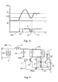
- the test signal SC comprises a first digital logic level 1 N when the tension VN1 in the intermediate node N1 is greater than a predetermined reference value Vref, and a second digital logic level 2N when said voltage VN1 is smaller than said reference value Vref, as shown in Figures 3a and 3b .
- the switch S1 is closed for a predetermined closure time Ton, which may be approximately four micro-seconds, for example, but which may also be longer or shorter depending on the manufacturer's requirements, and is opened at the end of the closure time Ton.
- Ton a predetermined closure time
- the test signal SC is evaluated during, at the most, a predetermined waiting time Te to determine the presence or absence of a vessel on the induction surface of the apparatus, it being determined that a vessel is disposed on the induction surface if, during the waiting time Te, the test signal SC maintains its digital logic level. If, on the other hand, during said waiting time Te said test signal SC changes its digital logic level, it is determined that no vessel is disposed on the induction surface.
- Figure 3a shows the voltage VN1 in the intermediate node N1, with no vessel disposed on the induction surface.
- the voltage VN1 in the intermediate node N1 is substantially equal to zero as the switch S1 connects said intermediate node N1 to the reference voltage GND.
- the switch S1 is opened and the voltage VN1 shows a sinusoidal behaviour. Due to said behaviour the value of the voltage VN1 falls after reaching a maximum point, which in the event of the absence of a vessel can fall to approximately zero volts (the value then increases again, being stabilized in a specific offset value Vo greater than the reference value Vref).
- the test signal SC When the voltage N1 rises above the reference value Vref, the test signal SC comprises the first digital logic level 1N, and in the event that no vessel is disposed on the induction surface, when the voltage VN1 reaches the reference value Vref the test signal SC moves to the second digital logic level 2N, changing its digital logic level.
- Figure 3b shows the voltage VN1 in the intermediate node N1, with a vessel disposed on the induction surface.
- the voltage VN1 is substantially equal to zero as the switch S1 connects the intermediate node N1 to the reference voltage GND.
- the switch S1 is opened and the voltage VN1 shows a sinusoidal behaviour, with the result that its value falls after reaching a maximum point.
- the voltage VN1 decreases being stabilised directly at the offset value Vo, with a certain oscillation dependent on the closure time Ton and the resistance of the vessel.
- the manufacturer pre-selects the predetermined reference value Vref in order to bring about the change in the digital logic level of the test signal SC that is smaller than the offset value Vo, with the result that when a vessel is disposed on the induction surface, the voltage VN1 does not fall to the reference value Vref, remaining instead at a greater value (offset value Vo), and the test signal SC maintains its digital logic level.
- the test signal SC comprises the first digital logic level 1 N when the voltage VN1 rises above the reference value Vref.
- the control method of the invention is also adapted to determine said size and/or quality.
- the voltage VN1 remains stable at the offset value Vo but comprises a plurality of oscillations, as shown in Figure 3b .
- the amplitude of the oscillations depends on the resistance of the vessel and closure time Ton applied to the switch S1, with the result that the method of the invention may repeat the steps of closing the switch S1 for a time interval Ton greater than the previous time interval Ton, opening said switch S1 at the end of the corresponding closure time Ton, and, with the switch S1 opened, evaluating the test signal SC in order to determine whether the test signal SC maintains its digital logic level during the waiting time Te, to evaluate when the oscillation is of an amplitude that reaches the reference value Vref thereby causing the test signal SC to change its digital logic level, as shown in Figure 3c .
- one closure time Ton may be four micro-seconds, the second one eight micro-seconds, and the third one 12 micro-seconds... More or less power may thus be applied depending on the degree of resistivity of the vessel.
- the process may be repeated as many times as is necessary in order to detect a modification in the test signal SC, with the process coming to an end when said change is detected, or the number of repetitions limited to a predetermined maximum number of times (five, for example), with the process coming to an end when said change is detected or when the predetermined number of times is repeated, according to the circumstances arising beforehand. In this latter case, if no change is detected in the digital logic level of the test signal SC, a maximum or minimum quality or size is determined by default.
- the test signal SC is evaluated once said voltage VN1 has exceeded said reference value Vref and comprises the first digital logic level 1 N. Once the test signal SC comprises said first digital logic level 1N, the presence or not of a vessel is determined at the end of a waiting time Te, it being evaluated during said waiting time Te if the digital logic level of the test signal SC has changed or not.
- the presence or absence of a vessel may be determined at the end of the waiting time Te, although preferably the presence of a vessel is determined at the end of said waiting time Te and the absence of a vessel at the same time as the digital logic level of the test signal SC changes, without waiting for the waiting time Te to end.
- the only condition applying to the duration of the waiting time Te is that it must be greater than a minimum time Tmin required by the voltage VN1 to reach the reference value Vref in the event that there is no vessel, shown in Figure 3a .
- Any desired waiting time Te may be predetermined provided that it is greater than said minimum time. This ensures that in the event of the absence of a vessel the test signal SC changes digital logic level.
- the waiting time Te starts preferably, as shown in Figure 3a , at the moment at which the voltage VN1 exceeds the reference value Vref (when the test signal SC moves from the second digital logic level 2N to the first digital logic level 1 N), but it may also start at the moment at which the switch S1 is opened.
- the change in the digital logic level contemplated in order to determine that there is no vessel disposed on the induction surface would be the change from the first digital logic level 1 N to the second digital logic level 2N, the change from said second digital logic level 2N to said first digital logic level 1 N not being taken into account.
- the induction apparatus of the invention comprises control means 1 adapted to cause the opening and closure of the switch S1 when required.
- the test signal SC preferably communicates with said control means 1, said control means 1 being the means that determine whether the digital logic level of said test signal SC changes during the waiting time Te or not, and the means that determine whether a vessel is disposed on the induction surface of the apparatus or not.
- the apparatus 100 may comprise additional control means (not shown in the figures) which receives the test signal SC, which are adapted to be the means that determine the presence or not of a vessel on the induction surface instead of the control means 1 that are adapted to cause the opening and closure of the switch S1.
- the control means 1 comprise a control device such as a micro-processor, a microcontroller or equivalent device, and the times Ton and Te are preferably generated by means of timers pre-programmed by the manufacturer in said control means 1.
- the control means 1 are adapted to determine that there is no vessel disposed on the induction surface of the apparatus at the same time as the test signal SC changes its digital logic level, without waiting for the waiting time Te to end, the control means 1 used comprise at least one interruption pin, the test signal SC being connected to said interruption pin.
- Said interruption pin is associated to the timer of the waiting time Te, and if there is no vessel, when the test signal SC changes level, as said test signal SC is connected to a interruption pin, the edge F produced by said change causes the timer to stop counting, said control means 1 determining the absence of the vessel at that instant.
- the induction apparatus of the invention also comprises a generator 3 for generating the test signal SC.
- Said generator 3 comprises a second switch S2 that is opened when the voltage VN1 in the intermediate node N1 is greater than the reference value Vref, the test signal SC being associated to the first digital logic level 1 N with the second switch S2 in this open position, and which is closed when said voltage VN1 is smaller than said reference value Vref, the test signal SC being associated to the second digital logic level 2N with the second switch S2 in this closed position.
- Figure 4 shows a preferred embodiment of the generator 3 of the induction apparatus, which comprises a voltage divider 2 parallel to the switch S1, formed by a first resistance R1 and a second resistance R2 disposed in series, with the reference value Vref for the change of the digital logic level of the test signal SC depending on the value of both resistances R1 and R2.
- the second switch S2 corresponds with a PNP bipolar transistor, the base of which is connected to a second node N2 between both resistances R1 and R2, the collector of which is connected to the reference voltage GND, and the emitter of which is connected to a supply voltage VCC, preferably approximately equal to five volts, by means of a third resistance R3, the test signal SC being connected to said emitter.
- test signal SC when the test signal SC is connected to the digital logic level 2N (the voltage VN1 is smaller than the reference value Vref), a current flows between the emitter and the base of the PNP bipolar transistor, and the test signal SC comprises a logic zero.
- test signal SC when the test signal SC is connected to the first digital logic level 1 N (the voltage VN1 is greater than the reference value Vref), no current flows between the emitter and the base of the PNP bipolar transistor and the test signal SC comprises a logic one due to the connection of the emitter to the supply voltage VCC.
- the change of level moves from a logic one (the first digital logic level 1 N) to a logic zero (the second digital logic level 2N), and if the control means 1 detect the change in level by means of an edge F, said edge F is a falling edge.
Claims (15)
- Procédé de commande pour un appareil à induction, l'appareil comprenant :au moins une bobine d'induction (L1),au moins un condensateur (C1) connecté en parallèle avec la bobine d'induction (L1), ladite bobine d'induction (L1) et le condensateur (C1) formant un circuit résonnant parallèle (LC), etau moins un commutateur (S1) connecté en série avec le circuit résonnant parallèle (LC), entre ledit circuit résonnant parallèle (LC) et une tension de référence (GND),caractérisé en ce queun signal de test numérique (SC) fonction de la tension présente dans un noeud intermédiaire (N1) disposé entre le commutateur (S1) et le circuit résonnant parallèle (LC) est généré, lequel comprend un premier niveau logique numérique (1 N) lorsque la tension (VN1) dans le noeud intermédiaire (N1) est supérieure à une valeur de référence (Vref) prédéterminée et un deuxième niveau logique numérique (2N) lorsque ladite tension (VN1) est inférieure à ladite valeur de référence (Vref),le commutateur (S1) est fermé pendant un temps de fermeture (Ton) prédéterminé, ledit commutateur (S1) est ouvert à la fin du temps de fermeture (Ton), etle commutateur (S1) étant ouvert, le signal de test (SC) est évalué pour déterminer la présence ou l'absence d'un récipient sur la bobine d'induction (L1) pendant, au plus, un temps d'attente (Te) prédéterminé, la présence d'un récipient étant déterminée si, pendant ledit temps d'attente (Te), le signal de test (SC) maintient son niveau logique numérique.
- Procédé selon la revendication 1, dans lequel il est déterminé que le niveau logique numérique du signal de test (SC) est maintenu si, à la fin du temps d'attente (Te), ledit signal de test (SC) comprend le premier niveau logique numérique (1 N).
- Procédé selon la revendication 1, dans lequel il est déterminé que le niveau logique numérique du signal de test (SC) est maintenu si aucun front descendant (F) dans ledit signal de test (SC) n'est détecté pendant le temps d'attente (Te).
- Procédé selon l'une quelconque des revendications précédentes, dans lequel le temps d'attente (Te) est supérieur à un temps minimum (Tmin) nécessaire pour que la tension (VN1) dans le noeud intermédiaire (N1) disposé entre le commutateur (S1) et le circuit résonnant parallèle (LC) passe du premier niveau logique numérique (1 N) au deuxième niveau logique numérique (2N).
- Procédé selon l'une quelconque des revendications précédentes, dans lequel le premier niveau logique numérique (1 N) correspond à un 1 logique, et le deuxième niveau logique numérique (2N) correspond à un 0 logique.
- Procédé selon l'une quelconque des revendications précédentes, dans lequel, si la présence d'un récipient est déterminée et jusqu'à ce qu'il soit détecté que le signal de test (SC) change de niveau logique numérique pendant le temps d'attente (Te), le processus de fermeture du commutateur (S1) pendant un intervalle de temps (Ton) supérieur à l'intervalle de temps (Ton) précédent, d'ouverture dudit commutateur (S1) à la fin du temps de fermeture (Ton) correspondant, et, le commutateur (S1) étant ouvert, d'évaluation du signal de test (SC) pour déterminer s'il a changé de niveau logique numérique pendant le temps d'attente (Te) est répété, la taille et/ou la qualité du récipient étant déterminées en fonction du temps de fermeture (Ton) nécessaire pour que ledit signal de test change de niveau logique numérique.
- Procédé selon l'une quelconque des revendications 1 à 5, dans lequel, si la présence d'un récipient est déterminée, le processus de fermeture du commutateur (S1) pendant un intervalle de temps (Ton) supérieur à l'intervalle de temps (Ton) précédent, d'ouverture dudit commutateur (S1) à la fin du temps de fermeture (Ton) correspondant, et, le commutateur (S1) étant ouvert, d'évaluation du signal de test (SC) pour déterminer si le signal de test (SC) change de niveau logique numérique pendant le temps d'attente (Te) est répété un nombre de fois prédéterminé maximum, la taille et/ou la qualité du récipient étant déterminées en fonction du temps de fermeture (Ton) nécessaire pour que ledit signal de test change de niveau logique numérique.
- Appareil à induction comprenant :au moins une bobine d'induction (L1),au moins un condensateur (C1) connecté en parallèle avec la bobine d'induction (L1), ladite bobine d'induction (L1) et le condensateur (C1) formant un circuit résonnant parallèle (LC),au moins un commutateur (S1) connecté en série avec le circuit résonnant parallèle (LC), entre ledit circuit résonnant parallèle (LC) et une tension de référence (GND), etdes moyens de commande (1) conçus pour ouvrir et fermer le commutateur (S1),caractérisé en ce queil comprend également un générateur (3) pour générer un signal de test numérique (SC) qui comprend un premier niveau logique numérique (1 N) lorsque la tension dans un noeud intermédiaire (N1) disposé entre le commutateur (S1) et le circuit résonnant parallèle (LC) est supérieure à une valeur de référence (Vref) prédéterminée, et un deuxième niveau logique numérique (2N) lorsque la tension dans le noeud intermédiaire (N1) est inférieure à ladite valeur de référence (Vref),les moyens de commande (1) étant conçus pour fermer le commutateur (S1) pendant un temps de fermeture (Ton) prédéterminé, pour ouvrir ledit commutateur (S1) à la fin du temps de fermeture (Ton), et, le commutateur (S1) étant ouvert pour évaluer le signal de test (SC) afin de déterminer la présence ou l'absence d'un récipient sur la bobine d'induction (L1) pendant un temps d'attente maximum (Te) prédéterminé, lesdits moyens de commande (1) déterminant la présence d'un récipient si, pendant le temps d'attente (Te), ils détectent que le signal de test (SC) maintient son niveau logique numérique.
- Appareil selon la revendication 8, dans lequel les moyens de commande (1) comprennent une broche d'interruption, le signal de test (SC) étant connecté à ladite broche d'interruption.
- Appareil selon l'une ou l'autre des revendications 8 ou 9, dans lequel le générateur (3) comprend un deuxième commutateur (S2) qui est ouvert lorsqu'une tension (VN1) dans le noeud intermédiaire (N1) est supérieure à la valeur de référence (Vref), le signal de test (SC) étant connecté au premier niveau logique numérique (1 N), et qui est fermé lorsque ladite tension (VN1) est inférieure à ladite valeur de référence (Vref), le signal de test (SC) étant connecté au deuxième niveau logique numérique (2N).
- Appareil selon la revendication 10, dans lequel le générateur (3) comprend un diviseur de tension (2) formé par deux résistances (R1, R2) en série disposées en parallèle avec le commutateur (S1), le deuxième commutateur (S2) comprenant un transistor bipolaire PNP, et sa base étant connectée au deuxième noeud (N2) disposé entre les deux résistances (R1, R2), son collecteur étant connecté au deuxième niveau logique numérique (2N), et son émetteur étant connecté au premier niveau logique numérique (1 N).
- Appareil selon l'une quelconque des revendications 8 à 11, dans lequel le premier niveau logique numérique (1 N) correspond à une tension d'alimentation (VCC), comprenant un 1 logique, et le deuxième niveau logique numérique (2N) correspond à la tension de référence (GND), comprenant un 0 logique.
- Appareil selon l'une quelconque des revendications 8 à 12, dans lequel le commutateur (S1) est un IGBT.
- Appareil selon l'une quelconque des revendications 8 à 13, dans lequel si la présence d'un récipient est détectée et jusqu'à ce qu'il soit détecté que le signal de test (SC) change de niveau logique numérique pendant le temps d'attente (Te), les moyens de commande (1) sont conçus pour répéter le processus de fermeture du commutateur (S1) pendant un intervalle de temps (Ton) supérieur à l'intervalle de temps (Ton) précédent, d'ouverture dudit commutateur (S1) à la fin du temps de fermeture (Ton) correspondant, et, le commutateur (S1) étant ouvert, d'évaluation du signal de test (SC) pour déterminer s'il a changé de niveau logique numérique pendant le temps d'attente (Te), lesdits moyens de commande (1) déterminant la taille et/ou la qualité du récipient en fonction du temps de fermeture (Ton) nécessaire pour que ledit signal de test change de niveau logique numérique.
- Appareil selon l'une quelconque des revendications 8 à 13, dans lequel, si la présence d'un récipient est déterminée, les moyens de commande (1) sont conçus pour répéter le processus de fermeture du commutateur (S1) pendant un intervalle de temps (Ton) supérieur à l'intervalle de temps (Ton) précédent, d'ouverture dudit commutateur (S1) à la fin du temps de fermeture (Ton) correspondant, et, le commutateur (S1) étant ouvert, d'évaluation du signal de test (SC) pour déterminer si le signal de test (SC) change de niveau logique numérique pendant le temps d'attente (Te), un nombre de fois prédéterminé maximum, lesdits moyens de commande (1) déterminant la taille et/ou la qualité du récipient en fonction du temps de fermeture (Ton) nécessaire pour que ledit signal de test change de niveau logique numérique.
Priority Applications (5)
| Application Number | Priority Date | Filing Date | Title |
|---|---|---|---|
| ES09380143T ES2382767T3 (es) | 2009-08-05 | 2009-08-05 | Procedimiento de control para un aparato de inducción, y aparato de inducción |
| AT09380143T ATE554632T1 (de) | 2009-08-05 | 2009-08-05 | Steuerungsverfahren für eine induktionsvorrichtung und induktionsvorrichtung |
| EP09380143A EP2282606B1 (fr) | 2009-08-05 | 2009-08-05 | Procédé de commande pour un appareil à induction et appareil à induction |
| US12/850,614 US8405411B2 (en) | 2009-08-05 | 2010-08-04 | Control method for an induction apparatus, and induction apparatus |
| CA2712186A CA2712186C (fr) | 2009-08-05 | 2010-08-05 | Methode de controle pour un appareil a induction et appareil proprement dit |
Applications Claiming Priority (1)
| Application Number | Priority Date | Filing Date | Title |
|---|---|---|---|
| EP09380143A EP2282606B1 (fr) | 2009-08-05 | 2009-08-05 | Procédé de commande pour un appareil à induction et appareil à induction |
Publications (2)
| Publication Number | Publication Date |
|---|---|
| EP2282606A1 EP2282606A1 (fr) | 2011-02-09 |
| EP2282606B1 true EP2282606B1 (fr) | 2012-04-18 |
Family
ID=42173568
Family Applications (1)
| Application Number | Title | Priority Date | Filing Date |
|---|---|---|---|
| EP09380143A Active EP2282606B1 (fr) | 2009-08-05 | 2009-08-05 | Procédé de commande pour un appareil à induction et appareil à induction |
Country Status (5)
| Country | Link |
|---|---|
| US (1) | US8405411B2 (fr) |
| EP (1) | EP2282606B1 (fr) |
| AT (1) | ATE554632T1 (fr) |
| CA (1) | CA2712186C (fr) |
| ES (1) | ES2382767T3 (fr) |
Families Citing this family (7)
| Publication number | Priority date | Publication date | Assignee | Title |
|---|---|---|---|---|
| EP2774452A1 (fr) | 2011-11-03 | 2014-09-10 | Arçelik Anonim Sirketi | Cuiseur à induction |
| US9671111B2 (en) | 2013-03-13 | 2017-06-06 | Ghp Group, Inc. | Fuel selector valve with shutter mechanism for a gas burner unit |
| EP2999302B1 (fr) * | 2014-09-18 | 2019-11-27 | Electrolux Appliances Aktiebolag | Plaque de cuisson à induction et procédé pour détecter la présence d'une batterie de cuisine |
| CN106678899A (zh) * | 2015-11-11 | 2017-05-17 | 佛山市顺德区美的电热电器制造有限公司 | 电磁加热系统及用于电磁加热系统的检测锅具方法和装置 |
| WO2017149055A1 (fr) | 2016-03-04 | 2017-09-08 | Arcelik Anonim Sirketi | Circuit de commande de puissance de cuisinière à induction |
| TR201602883A2 (tr) | 2016-03-04 | 2017-09-21 | Arcelik As | İndüksi̇yon isiticili ocak güç kontrol devresi̇ |
| KR20220108587A (ko) * | 2021-01-27 | 2022-08-03 | 엘지전자 주식회사 | 유도 가열 장치 및 유도 가열 장치의 제어 방법 |
Family Cites Families (1)
| Publication number | Priority date | Publication date | Assignee | Title |
|---|---|---|---|---|
| DE102005050036A1 (de) * | 2005-10-14 | 2007-05-31 | E.G.O. Elektro-Gerätebau GmbH | Induktionsheizeinrichtung und zugehöriges Betriebs- und Topferkennungsverfahren |
-
2009
- 2009-08-05 ES ES09380143T patent/ES2382767T3/es active Active
- 2009-08-05 EP EP09380143A patent/EP2282606B1/fr active Active
- 2009-08-05 AT AT09380143T patent/ATE554632T1/de active
-
2010
- 2010-08-04 US US12/850,614 patent/US8405411B2/en active Active
- 2010-08-05 CA CA2712186A patent/CA2712186C/fr active Active
Also Published As
| Publication number | Publication date |
|---|---|
| EP2282606A1 (fr) | 2011-02-09 |
| CA2712186C (fr) | 2016-08-30 |
| CA2712186A1 (fr) | 2011-02-05 |
| US8405411B2 (en) | 2013-03-26 |
| ES2382767T3 (es) | 2012-06-13 |
| US20110031989A1 (en) | 2011-02-10 |
| ATE554632T1 (de) | 2012-05-15 |
Similar Documents
| Publication | Publication Date | Title |
|---|---|---|
| EP2282606B1 (fr) | Procédé de commande pour un appareil à induction et appareil à induction | |
| JP5586433B2 (ja) | 誘導加熱コイルによって加熱される調理容器ベースの温度を決定するための方法および誘導加熱装置 | |
| US4820891A (en) | Induction heated cooking apparatus | |
| US8901466B2 (en) | Induction heating device and associated operating and saucepan detection method | |
| EP2845416B1 (fr) | Procédés de détection et d'identification d'un récepteur dans un système de transfert de puissance inductif | |
| US20150326129A1 (en) | Flyback power converter and control circuit thereof | |
| US4931609A (en) | High-frequency heating apparatus having a digital-controlled inverter | |
| WO2013064331A1 (fr) | Cuiseur à induction | |
| US5424514A (en) | Apparatus for sensing small object in high-frequency induction heating cooker | |
| US20200323048A1 (en) | Induction heating apparatus | |
| KR102641089B1 (ko) | 용기 감지 정확도 개선을 위한 단일 펄스 예비 테스트 방법 | |
| EP1592285A1 (fr) | Dispositif de commande d'un onduleur pour un appareil de cuisson à induction | |
| KR102661286B1 (ko) | 공진 전류를 이용한 용기 감지 방법 | |
| CN105230120A (zh) | 感应加热炉灶面 | |
| CN110461193B (zh) | 电磁感应加热烹调器 | |
| KR100204886B1 (ko) | 고주파 유도가열 조리장치 | |
| JPH04371108A (ja) | 誘導加熱調理器の鍋検知装置 | |
| CN111954327B (zh) | 感应线圈结构单元和控制感应线圈结构单元的感应式加热过程的方法 | |
| KR960004836B1 (ko) | 전자조리기 | |
| KR20200009990A (ko) | 용기 감지 기능을 수행하는 유도 가열 장치 | |
| JP2742147B2 (ja) | 誘導加熱装置 | |
| KR940000427Y1 (ko) | 유도 가열조리기의 온/오프시 보호회로 | |
| KR200437999Y1 (ko) | 유도가열 조리기기의 보호 장치 | |
| KR100284435B1 (ko) | 유도가열밥솥의 전력제어장치 | |
| KR100266616B1 (ko) | 고출력 유도가열조리기 |
Legal Events
| Date | Code | Title | Description |
|---|---|---|---|
| PUAI | Public reference made under article 153(3) epc to a published international application that has entered the european phase |
Free format text: ORIGINAL CODE: 0009012 |
|
| AK | Designated contracting states |
Kind code of ref document: A1 Designated state(s): AT BE BG CH CY CZ DE DK EE ES FI FR GB GR HR HU IE IS IT LI LT LU LV MC MK MT NL NO PL PT RO SE SI SK SM TR |
|
| AX | Request for extension of the european patent |
Extension state: AL BA RS |
|
| 17P | Request for examination filed |
Effective date: 20110304 |
|
| GRAP | Despatch of communication of intention to grant a patent |
Free format text: ORIGINAL CODE: EPIDOSNIGR1 |
|
| RIC1 | Information provided on ipc code assigned before grant |
Ipc: H05B 6/06 20060101AFI20120120BHEP |
|
| GRAS | Grant fee paid |
Free format text: ORIGINAL CODE: EPIDOSNIGR3 |
|
| GRAA | (expected) grant |
Free format text: ORIGINAL CODE: 0009210 |
|
| AK | Designated contracting states |
Kind code of ref document: B1 Designated state(s): AT BE BG CH CY CZ DE DK EE ES FI FR GB GR HR HU IE IS IT LI LT LU LV MC MK MT NL NO PL PT RO SE SI SK SM TR |
|
| REG | Reference to a national code |
Ref country code: GB Ref legal event code: FG4D |
|
| REG | Reference to a national code |
Ref country code: CH Ref legal event code: EP |
|
| REG | Reference to a national code |
Ref country code: IE Ref legal event code: FG4D |
|
| REG | Reference to a national code |
Ref country code: AT Ref legal event code: REF Ref document number: 554632 Country of ref document: AT Kind code of ref document: T Effective date: 20120515 |
|
| REG | Reference to a national code |
Ref country code: ES Ref legal event code: FG2A Ref document number: 2382767 Country of ref document: ES Kind code of ref document: T3 Effective date: 20120613 |
|
| REG | Reference to a national code |
Ref country code: DE Ref legal event code: R096 Ref document number: 602009006444 Country of ref document: DE Effective date: 20120614 |
|
| REG | Reference to a national code |
Ref country code: NL Ref legal event code: VDEP Effective date: 20120418 |
|
| REG | Reference to a national code |
Ref country code: AT Ref legal event code: MK05 Ref document number: 554632 Country of ref document: AT Kind code of ref document: T Effective date: 20120418 |
|
| LTIE | Lt: invalidation of european patent or patent extension |
Effective date: 20120418 |
|
| PG25 | Lapsed in a contracting state [announced via postgrant information from national office to epo] |
Ref country code: IS Free format text: LAPSE BECAUSE OF FAILURE TO SUBMIT A TRANSLATION OF THE DESCRIPTION OR TO PAY THE FEE WITHIN THE PRESCRIBED TIME-LIMIT Effective date: 20120818 Ref country code: LT Free format text: LAPSE BECAUSE OF FAILURE TO SUBMIT A TRANSLATION OF THE DESCRIPTION OR TO PAY THE FEE WITHIN THE PRESCRIBED TIME-LIMIT Effective date: 20120418 Ref country code: NO Free format text: LAPSE BECAUSE OF FAILURE TO SUBMIT A TRANSLATION OF THE DESCRIPTION OR TO PAY THE FEE WITHIN THE PRESCRIBED TIME-LIMIT Effective date: 20120718 Ref country code: CY Free format text: LAPSE BECAUSE OF FAILURE TO SUBMIT A TRANSLATION OF THE DESCRIPTION OR TO PAY THE FEE WITHIN THE PRESCRIBED TIME-LIMIT Effective date: 20120418 Ref country code: PL Free format text: LAPSE BECAUSE OF FAILURE TO SUBMIT A TRANSLATION OF THE DESCRIPTION OR TO PAY THE FEE WITHIN THE PRESCRIBED TIME-LIMIT Effective date: 20120418 Ref country code: FI Free format text: LAPSE BECAUSE OF FAILURE TO SUBMIT A TRANSLATION OF THE DESCRIPTION OR TO PAY THE FEE WITHIN THE PRESCRIBED TIME-LIMIT Effective date: 20120418 Ref country code: SE Free format text: LAPSE BECAUSE OF FAILURE TO SUBMIT A TRANSLATION OF THE DESCRIPTION OR TO PAY THE FEE WITHIN THE PRESCRIBED TIME-LIMIT Effective date: 20120418 |
|
| PG25 | Lapsed in a contracting state [announced via postgrant information from national office to epo] |
Ref country code: SI Free format text: LAPSE BECAUSE OF FAILURE TO SUBMIT A TRANSLATION OF THE DESCRIPTION OR TO PAY THE FEE WITHIN THE PRESCRIBED TIME-LIMIT Effective date: 20120418 Ref country code: LV Free format text: LAPSE BECAUSE OF FAILURE TO SUBMIT A TRANSLATION OF THE DESCRIPTION OR TO PAY THE FEE WITHIN THE PRESCRIBED TIME-LIMIT Effective date: 20120418 Ref country code: PT Free format text: LAPSE BECAUSE OF FAILURE TO SUBMIT A TRANSLATION OF THE DESCRIPTION OR TO PAY THE FEE WITHIN THE PRESCRIBED TIME-LIMIT Effective date: 20120820 Ref country code: HR Free format text: LAPSE BECAUSE OF FAILURE TO SUBMIT A TRANSLATION OF THE DESCRIPTION OR TO PAY THE FEE WITHIN THE PRESCRIBED TIME-LIMIT Effective date: 20120418 |
|
| PG25 | Lapsed in a contracting state [announced via postgrant information from national office to epo] |
Ref country code: BE Free format text: LAPSE BECAUSE OF FAILURE TO SUBMIT A TRANSLATION OF THE DESCRIPTION OR TO PAY THE FEE WITHIN THE PRESCRIBED TIME-LIMIT Effective date: 20120418 |
|
| PG25 | Lapsed in a contracting state [announced via postgrant information from national office to epo] |
Ref country code: NL Free format text: LAPSE BECAUSE OF FAILURE TO SUBMIT A TRANSLATION OF THE DESCRIPTION OR TO PAY THE FEE WITHIN THE PRESCRIBED TIME-LIMIT Effective date: 20120418 Ref country code: AT Free format text: LAPSE BECAUSE OF FAILURE TO SUBMIT A TRANSLATION OF THE DESCRIPTION OR TO PAY THE FEE WITHIN THE PRESCRIBED TIME-LIMIT Effective date: 20120418 Ref country code: CZ Free format text: LAPSE BECAUSE OF FAILURE TO SUBMIT A TRANSLATION OF THE DESCRIPTION OR TO PAY THE FEE WITHIN THE PRESCRIBED TIME-LIMIT Effective date: 20120418 Ref country code: RO Free format text: LAPSE BECAUSE OF FAILURE TO SUBMIT A TRANSLATION OF THE DESCRIPTION OR TO PAY THE FEE WITHIN THE PRESCRIBED TIME-LIMIT Effective date: 20120418 Ref country code: EE Free format text: LAPSE BECAUSE OF FAILURE TO SUBMIT A TRANSLATION OF THE DESCRIPTION OR TO PAY THE FEE WITHIN THE PRESCRIBED TIME-LIMIT Effective date: 20120418 Ref country code: SK Free format text: LAPSE BECAUSE OF FAILURE TO SUBMIT A TRANSLATION OF THE DESCRIPTION OR TO PAY THE FEE WITHIN THE PRESCRIBED TIME-LIMIT Effective date: 20120418 Ref country code: DK Free format text: LAPSE BECAUSE OF FAILURE TO SUBMIT A TRANSLATION OF THE DESCRIPTION OR TO PAY THE FEE WITHIN THE PRESCRIBED TIME-LIMIT Effective date: 20120418 |
|
| PLBE | No opposition filed within time limit |
Free format text: ORIGINAL CODE: 0009261 |
|
| STAA | Information on the status of an ep patent application or granted ep patent |
Free format text: STATUS: NO OPPOSITION FILED WITHIN TIME LIMIT |
|
| 26N | No opposition filed |
Effective date: 20130121 |
|
| PG25 | Lapsed in a contracting state [announced via postgrant information from national office to epo] |
Ref country code: MC Free format text: LAPSE BECAUSE OF NON-PAYMENT OF DUE FEES Effective date: 20120831 |
|
| REG | Reference to a national code |
Ref country code: DE Ref legal event code: R097 Ref document number: 602009006444 Country of ref document: DE Effective date: 20130121 |
|
| REG | Reference to a national code |
Ref country code: IE Ref legal event code: MM4A |
|
| PG25 | Lapsed in a contracting state [announced via postgrant information from national office to epo] |
Ref country code: BG Free format text: LAPSE BECAUSE OF FAILURE TO SUBMIT A TRANSLATION OF THE DESCRIPTION OR TO PAY THE FEE WITHIN THE PRESCRIBED TIME-LIMIT Effective date: 20120718 Ref country code: IE Free format text: LAPSE BECAUSE OF NON-PAYMENT OF DUE FEES Effective date: 20120805 |
|
| PG25 | Lapsed in a contracting state [announced via postgrant information from national office to epo] |
Ref country code: MT Free format text: LAPSE BECAUSE OF FAILURE TO SUBMIT A TRANSLATION OF THE DESCRIPTION OR TO PAY THE FEE WITHIN THE PRESCRIBED TIME-LIMIT Effective date: 20120418 |
|
| REG | Reference to a national code |
Ref country code: CH Ref legal event code: PL |
|
| GBPC | Gb: european patent ceased through non-payment of renewal fee |
Effective date: 20130805 |
|
| PG25 | Lapsed in a contracting state [announced via postgrant information from national office to epo] |
Ref country code: TR Free format text: LAPSE BECAUSE OF FAILURE TO SUBMIT A TRANSLATION OF THE DESCRIPTION OR TO PAY THE FEE WITHIN THE PRESCRIBED TIME-LIMIT Effective date: 20120418 Ref country code: CH Free format text: LAPSE BECAUSE OF NON-PAYMENT OF DUE FEES Effective date: 20130831 Ref country code: LI Free format text: LAPSE BECAUSE OF NON-PAYMENT OF DUE FEES Effective date: 20130831 |
|
| PG25 | Lapsed in a contracting state [announced via postgrant information from national office to epo] |
Ref country code: LU Free format text: LAPSE BECAUSE OF NON-PAYMENT OF DUE FEES Effective date: 20120805 Ref country code: SM Free format text: LAPSE BECAUSE OF FAILURE TO SUBMIT A TRANSLATION OF THE DESCRIPTION OR TO PAY THE FEE WITHIN THE PRESCRIBED TIME-LIMIT Effective date: 20120418 |
|
| PG25 | Lapsed in a contracting state [announced via postgrant information from national office to epo] |
Ref country code: GB Free format text: LAPSE BECAUSE OF NON-PAYMENT OF DUE FEES Effective date: 20130805 Ref country code: HU Free format text: LAPSE BECAUSE OF FAILURE TO SUBMIT A TRANSLATION OF THE DESCRIPTION OR TO PAY THE FEE WITHIN THE PRESCRIBED TIME-LIMIT Effective date: 20090805 |
|
| PG25 | Lapsed in a contracting state [announced via postgrant information from national office to epo] |
Ref country code: GR Free format text: LAPSE BECAUSE OF FAILURE TO SUBMIT A TRANSLATION OF THE DESCRIPTION OR TO PAY THE FEE WITHIN THE PRESCRIBED TIME-LIMIT Effective date: 20120418 |
|
| PG25 | Lapsed in a contracting state [announced via postgrant information from national office to epo] |
Ref country code: MK Free format text: LAPSE BECAUSE OF FAILURE TO SUBMIT A TRANSLATION OF THE DESCRIPTION OR TO PAY THE FEE WITHIN THE PRESCRIBED TIME-LIMIT Effective date: 20120418 |
|
| REG | Reference to a national code |
Ref country code: FR Ref legal event code: PLFP Year of fee payment: 8 |
|
| REG | Reference to a national code |
Ref country code: FR Ref legal event code: PLFP Year of fee payment: 9 |
|
| REG | Reference to a national code |
Ref country code: FR Ref legal event code: PLFP Year of fee payment: 10 |
|
| P01 | Opt-out of the competence of the unified patent court (upc) registered |
Effective date: 20230524 |
|
| PGFP | Annual fee paid to national office [announced via postgrant information from national office to epo] |
Ref country code: IT Payment date: 20230822 Year of fee payment: 15 Ref country code: ES Payment date: 20230901 Year of fee payment: 15 |
|
| PGFP | Annual fee paid to national office [announced via postgrant information from national office to epo] |
Ref country code: FR Payment date: 20230825 Year of fee payment: 15 Ref country code: DE Payment date: 20230829 Year of fee payment: 15 |