EP2282606B1 - Control method for an induction apparatus, and induction apparatus - Google Patents
Control method for an induction apparatus, and induction apparatus Download PDFInfo
- Publication number
- EP2282606B1 EP2282606B1 EP09380143A EP09380143A EP2282606B1 EP 2282606 B1 EP2282606 B1 EP 2282606B1 EP 09380143 A EP09380143 A EP 09380143A EP 09380143 A EP09380143 A EP 09380143A EP 2282606 B1 EP2282606 B1 EP 2282606B1
- Authority
- EP
- European Patent Office
- Prior art keywords
- switch
- logic level
- test signal
- digital logic
- ton
- Prior art date
- Legal status (The legal status is an assumption and is not a legal conclusion. Google has not performed a legal analysis and makes no representation as to the accuracy of the status listed.)
- Active
Links
- 230000006698 induction Effects 0.000 title claims abstract description 73
- 238000000034 method Methods 0.000 title claims abstract description 35
- 238000012360 testing method Methods 0.000 claims abstract description 81
- 239000003990 capacitor Substances 0.000 claims abstract description 15
- 230000001419 dependent effect Effects 0.000 claims abstract description 6
- 230000010355 oscillation Effects 0.000 description 6
- 238000011161 development Methods 0.000 description 4
- 239000000463 material Substances 0.000 description 3
- 230000007423 decrease Effects 0.000 description 2
- 238000011156 evaluation Methods 0.000 description 2
- XAGFODPZIPBFFR-UHFFFAOYSA-N aluminium Chemical compound [Al] XAGFODPZIPBFFR-UHFFFAOYSA-N 0.000 description 1
- 229910052782 aluminium Inorganic materials 0.000 description 1
- 239000004411 aluminium Substances 0.000 description 1
- 238000001514 detection method Methods 0.000 description 1
- 238000012986 modification Methods 0.000 description 1
- 230000004048 modification Effects 0.000 description 1
Images


Classifications
-
- H—ELECTRICITY
- H05—ELECTRIC TECHNIQUES NOT OTHERWISE PROVIDED FOR
- H05B—ELECTRIC HEATING; ELECTRIC LIGHT SOURCES NOT OTHERWISE PROVIDED FOR; CIRCUIT ARRANGEMENTS FOR ELECTRIC LIGHT SOURCES, IN GENERAL
- H05B6/00—Heating by electric, magnetic or electromagnetic fields
- H05B6/02—Induction heating
- H05B6/06—Control, e.g. of temperature, of power
- H05B6/062—Control, e.g. of temperature, of power for cooking plates or the like
-
- H—ELECTRICITY
- H05—ELECTRIC TECHNIQUES NOT OTHERWISE PROVIDED FOR
- H05B—ELECTRIC HEATING; ELECTRIC LIGHT SOURCES NOT OTHERWISE PROVIDED FOR; CIRCUIT ARRANGEMENTS FOR ELECTRIC LIGHT SOURCES, IN GENERAL
- H05B2213/00—Aspects relating both to resistive heating and to induction heating, covered by H05B3/00 and H05B6/00
- H05B2213/05—Heating plates with pan detection means
Abstract
Description
- The present invention relates to a control method for an induction apparatus, and more specifically to a method for detecting a vessel in an induction apparatus. The invention also relates to an induction apparatus adapted to carry out said method.
- Induction apparatuses comprise at least one induction surface upon which a vessel may be disposed and heated, said apparatuses comprising at least one induction coil disposed beneath the induction surface in order to heat said vessel. To heat the vessel, the induction coil is supplied by an alternating current. A magnetic field is generated as a result and this causes the generation of eddy currents through the vessel disposed on the induction surface, said eddy currents causing said vessel to heat up.
- There are various known alternatives for supplying the induction coil, the majority of which include a rectifier and a frequency converter for the rectified signal. The frequency converter generally comprises at least one switch, and in many cases a single switch is used, this being connected in series with a parallel resonant circuit formed by the induction coil and a capacitor.
- The drawback with this alternative is that it may cause the system to overheat or become damaged due to the use of a vessel made of an unsuitable material such as aluminium, for example, a material which offers high inductance and low resistance. It is important, therefore, that the induction apparatus includes a method capable of detecting the presence or absence of said vessel, and/or the quality (resistivity) (or size) of said vessel, the purpose being not to supply said induction coil with power when no vessel is disposed on the induction surface for example, or to supply it with power that is insufficient for the size or resistivity of the vessel disposed on said surface.
- Document
EP1935214A2 discloses an induction apparatus that comprises a method for detecting a vessel. In this method the voltage in an intermediate node between the switch and the parallel resonant circuit formed by a capacitor and the induction coil is determined, and it is important to close the switch when the voltage in the intermediate node reaches a minimum point and for a time interval determined by the voltage in said minimum point. The closure of the switch generates oscillations in the voltage of the intermediate node, and the presence or absence of the vessel is determined in accordance with the number of oscillations detected. - It is an object of this invention to provide a control method for an induction apparatus, as described in
claims 1 to 7, and to provide an induction apparatus adapted to carry out said method, as described in claims 8 to 15. - The control method of the invention is used to detect a vessel disposed on an induction apparatus. Said apparatus comprises at least one induction coil, upon which a vessel may be disposed and heated, at least one capacitor connected in parallel with the induction coil, said induction coil and the capacitor forming a parallel resonant circuit, and at least one switch connected in series with the parallel resonant circuit, between said parallel resonant circuit and a reference voltage.
- In the method of the invention, a digital test signal dependent on the voltage in an intermediate node disposed between the switch and the parallel resonant circuit is generated, the switch is closed during a predetermined closure time, said switch is opened at the end of said closure time, and, with the switch opened, the test signal is evaluated during a maximum predetermined waiting time in order to determine the presence or absence of a vessel on the induction coil. The test signal comprises a first digital logic level when the voltage in the intermediate node is greater than a predetermined reference value and a second digital logic level when said voltage is smaller than said reference value, and the presence of a vessel is determined if, during its evaluation, the test signal maintains its digital logic level.
- As a result, when a digital test signal dependent on the voltage in an intermediate node disposed between the switch and the parallel resonant circuit is generated and when a vessel is detected by means of the evaluation of said test signal, it is sufficient to wait, at the most, a determined waiting time in order to carry out said detection, it being evaluated whether said test signal has changed its digital logic level or not, without strict limitations such as the moment of closure of the switch or the duration of said closure, which may be selected arbitrarily by the manufacturer.
- These and other advantages and characteristics of the invention will be made evident in the light of the drawings and the detailed description thereof.
-
-
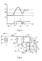
Figure 1 shows an induction circuit of an embodiment of the induction apparatus of the invention. -
Figure 2 shows a development of the voltage of a second capacitor of the induction circuit ofFigure 1 . -
Figure 3a shows the development of a test signal of the method of the invention, when there is no vessel disposed on the induction coil of the circuit ofFigure 1 . -
Figure 3b shows the development of a test signal of the method of the invention, when there is a vessel disposed on the induction coil of the circuit ofFigure 1 . -
Figure 3c shows the development of a test signal of the method of the invention, with the quality and/or size of a vessel disposed on the induction coil of the circuit ofFigure 1 being detected. -
Figure 4 shows a test signal generator of the circuit ofFigure 1 . - The control method of the invention is adapted to detect the presence of a vessel (not shown in the figures) in an induction apparatus (not shown in the figures), and as a result it detects whether a vessel has been disposed on an induction surface (not shown in the figures) of said apparatus. With reference to
Figure 1 , the apparatus comprises aninduction circuit 100 with at least one induction coil L1, upon which the induction surface is disposed, at least one capacitor C1 connected in parallel with the induction coil L1, said induction coil L1 and the capacitor C1 forming a parallel resonant circuit LC, and at least one switch S1, preferably an IGBT (Insulated Gate Bipolar Transistor), connected in series with the parallel resonant circuit LC between said parallel resonant circuit LC and a reference voltage GND. Theinduction circuit 100 also comprises two terminals A and B for the reception of an alternating voltage UN, abridge rectifier 4 to rectify the alternating voltage UN, a filter formed by a coil L2, and a second capacitor C2 that is charged with a capacitor voltage VC2, as shown inFigure 2 , when the circuit is supplied with the alternating voltage UN and the switch S1 is opened (the continuous line in saidFigure 2 ), and when the circuit is supplied with said alternating voltage UN and said switch S1 is closed (broken lines in saidFigure 2 ). - In a first moment, when the
induction circuit 100 is supplied with an alternating voltage UN, the switch S1 is preferably open. The method of the invention also involves the generation of a digital test signal SC dependent on a voltage VN1 present in an intermediate node N1 disposed between the switch S1 and the parallel resonant circuit LC. The test signal SC comprises a first digital logic level 1 N when the tension VN1 in the intermediate node N1 is greater than a predetermined reference value Vref, and a seconddigital logic level 2N when said voltage VN1 is smaller than said reference value Vref, as shown inFigures 3a and 3b . To detect the presence or absence of a vessel, the switch S1 is closed for a predetermined closure time Ton, which may be approximately four micro-seconds, for example, but which may also be longer or shorter depending on the manufacturer's requirements, and is opened at the end of the closure time Ton. Once the switch S1 is opened again, the test signal SC is evaluated during, at the most, a predetermined waiting time Te to determine the presence or absence of a vessel on the induction surface of the apparatus, it being determined that a vessel is disposed on the induction surface if, during the waiting time Te, the test signal SC maintains its digital logic level. If, on the other hand, during said waiting time Te said test signal SC changes its digital logic level, it is determined that no vessel is disposed on the induction surface. -
Figure 3a shows the voltage VN1 in the intermediate node N1, with no vessel disposed on the induction surface. During the closure time Ton, the voltage VN1 in the intermediate node N1 is substantially equal to zero as the switch S1 connects said intermediate node N1 to the reference voltage GND. When the closure time Ton ends, the switch S1 is opened and the voltage VN1 shows a sinusoidal behaviour. Due to said behaviour the value of the voltage VN1 falls after reaching a maximum point, which in the event of the absence of a vessel can fall to approximately zero volts (the value then increases again, being stabilized in a specific offset value Vo greater than the reference value Vref). When the voltage N1 rises above the reference value Vref, the test signal SC comprises the first digital logic level 1N, and in the event that no vessel is disposed on the induction surface, when the voltage VN1 reaches the reference value Vref the test signal SC moves to the seconddigital logic level 2N, changing its digital logic level. -
Figure 3b shows the voltage VN1 in the intermediate node N1, with a vessel disposed on the induction surface. During the closure time Ton, the voltage VN1 is substantially equal to zero as the switch S1 connects the intermediate node N1 to the reference voltage GND. When the closure time Ton ends, the switch S1 is opened and the voltage VN1 shows a sinusoidal behaviour, with the result that its value falls after reaching a maximum point. When a vessel is disposed on the induction surface, due to the fact that the vessel modifies the impedance of the induction coil L1, the voltage VN1 decreases being stabilised directly at the offset value Vo, with a certain oscillation dependent on the closure time Ton and the resistance of the vessel. The manufacturer pre-selects the predetermined reference value Vref in order to bring about the change in the digital logic level of the test signal SC that is smaller than the offset value Vo, with the result that when a vessel is disposed on the induction surface, the voltage VN1 does not fall to the reference value Vref, remaining instead at a greater value (offset value Vo), and the test signal SC maintains its digital logic level. The test signal SC comprises the first digital logic level 1 N when the voltage VN1 rises above the reference value Vref. When said voltage VN1 decreases again, said voltage VN1 does not fall below the reference value Vref and the test signal SC continues to maintain its first digital logic level 1N, it being possible to determine the presence of a vessel when the digital logic level of the test signal SC remains constant. - If the level of the test signal SC does not change, the presence of a vessel is determined but its size and/or quality cannot be determined, and the control method of the invention is also adapted to determine said size and/or quality. When said presence is detected, the voltage VN1 remains stable at the offset value Vo but comprises a plurality of oscillations, as shown in
Figure 3b . The amplitude of the oscillations depends on the resistance of the vessel and closure time Ton applied to the switch S1, with the result that the method of the invention may repeat the steps of closing the switch S1 for a time interval Ton greater than the previous time interval Ton, opening said switch S1 at the end of the corresponding closure time Ton, and, with the switch S1 opened, evaluating the test signal SC in order to determine whether the test signal SC maintains its digital logic level during the waiting time Te, to evaluate when the oscillation is of an amplitude that reaches the reference value Vref thereby causing the test signal SC to change its digital logic level, as shown inFigure 3c . The greater the closure time Ton necessary to ensure that the test signal SC changes its digital logic level is, the greater the resistance of the vessel disposed on the induction surface is and, therefore, bigger is said vessel or the material of said vessel is better for induction. For example, one closure time Ton may be four micro-seconds, the second one eight micro-seconds, and the third one 12 micro-seconds... More or less power may thus be applied depending on the degree of resistivity of the vessel. The process may be repeated as many times as is necessary in order to detect a modification in the test signal SC, with the process coming to an end when said change is detected, or the number of repetitions limited to a predetermined maximum number of times (five, for example), with the process coming to an end when said change is detected or when the predetermined number of times is repeated, according to the circumstances arising beforehand. In this latter case, if no change is detected in the digital logic level of the test signal SC, a maximum or minimum quality or size is determined by default. - When the switch S1 is closed the voltage VN1 is zero volts, with the result that when said switch S1 is opened again said voltage VN1 comprises during several seconds a voltage value lower than the reference value Vref which is associated to the change in the digital logic level of the test signal SC, and the test signal SC comprises the second
digital logic level 2N. According to the method of the invention, the test signal SC is evaluated once said voltage VN1 has exceeded said reference value Vref and comprises the firstdigital logic level 1 N. Once the test signal SC comprises said first digital logic level 1N, the presence or not of a vessel is determined at the end of a waiting time Te, it being evaluated during said waiting time Te if the digital logic level of the test signal SC has changed or not. The presence or absence of a vessel may be determined at the end of the waiting time Te, although preferably the presence of a vessel is determined at the end of said waiting time Te and the absence of a vessel at the same time as the digital logic level of the test signal SC changes, without waiting for the waiting time Te to end. The only condition applying to the duration of the waiting time Te is that it must be greater than a minimum time Tmin required by the voltage VN1 to reach the reference value Vref in the event that there is no vessel, shown inFigure 3a . Any desired waiting time Te may be predetermined provided that it is greater than said minimum time. This ensures that in the event of the absence of a vessel the test signal SC changes digital logic level. The waiting time Te starts preferably, as shown inFigure 3a , at the moment at which the voltage VN1 exceeds the reference value Vref (when the test signal SC moves from the seconddigital logic level 2N to the first digital logic level 1 N), but it may also start at the moment at which the switch S1 is opened. In this latter case, the change in the digital logic level contemplated in order to determine that there is no vessel disposed on the induction surface would be the change from the first digital logic level 1 N to the seconddigital logic level 2N, the change from said seconddigital logic level 2N to said first digital logic level 1 N not being taken into account. - The induction apparatus of the invention comprises control means 1 adapted to cause the opening and closure of the switch S1 when required. In addition, the test signal SC preferably communicates with said control means 1, said control means 1 being the means that determine whether the digital logic level of said test signal SC changes during the waiting time Te or not, and the means that determine whether a vessel is disposed on the induction surface of the apparatus or not. It is clear that the
apparatus 100 may comprise additional control means (not shown in the figures) which receives the test signal SC, which are adapted to be the means that determine the presence or not of a vessel on the induction surface instead of the control means 1 that are adapted to cause the opening and closure of the switch S1. - The control means 1 comprise a control device such as a micro-processor, a microcontroller or equivalent device, and the times Ton and Te are preferably generated by means of timers pre-programmed by the manufacturer in said control means 1. When the control means 1 are adapted to determine that there is no vessel disposed on the induction surface of the apparatus at the same time as the test signal SC changes its digital logic level, without waiting for the waiting time Te to end, the control means 1 used comprise at least one interruption pin, the test signal SC being connected to said interruption pin. Said interruption pin is associated to the timer of the waiting time Te, and if there is no vessel, when the test signal SC changes level, as said test signal SC is connected to a interruption pin, the edge F produced by said change causes the timer to stop counting, said control means 1 determining the absence of the vessel at that instant.
- The induction apparatus of the invention also comprises a
generator 3 for generating the test signalSC. Said generator 3 comprises a second switch S2 that is opened when the voltage VN1 in the intermediate node N1 is greater than the reference value Vref, the test signal SC being associated to the first digital logic level 1 N with the second switch S2 in this open position, and which is closed when said voltage VN1 is smaller than said reference value Vref, the test signal SC being associated to the seconddigital logic level 2N with the second switch S2 in this closed position.Figure 4 shows a preferred embodiment of thegenerator 3 of the induction apparatus, which comprises avoltage divider 2 parallel to the switch S1, formed by a first resistance R1 and a second resistance R2 disposed in series, with the reference value Vref for the change of the digital logic level of the test signal SC depending on the value of both resistances R1 and R2. In the preferred embodiment, the second switch S2 corresponds with a PNP bipolar transistor, the base of which is connected to a second node N2 between both resistances R1 and R2, the collector of which is connected to the reference voltage GND, and the emitter of which is connected to a supply voltage VCC, preferably approximately equal to five volts, by means of a third resistance R3, the test signal SC being connected to said emitter. Thus, in said preferred embodiment, when the test signal SC is connected to thedigital logic level 2N (the voltage VN1 is smaller than the reference value Vref), a current flows between the emitter and the base of the PNP bipolar transistor, and the test signal SC comprises a logic zero. On the other hand, when the test signal SC is connected to the first digital logic level 1 N (the voltage VN1 is greater than the reference value Vref), no current flows between the emitter and the base of the PNP bipolar transistor and the test signal SC comprises a logic one due to the connection of the emitter to the supply voltage VCC. In the preferred embodiment, therefore, the change of level moves from a logic one (the first digital logic level 1 N) to a logic zero (the seconddigital logic level 2N), and if the control means 1 detect the change in level by means of an edge F, said edge F is a falling edge.
Claims (15)
- Control method for an induction apparatus, the apparatus comprising
at least one induction coil (L1),
at least one capacitor (C1) connected in parallel with the induction coil (L1), said induction coil (L1) and the capacitor (C1) forming a parallel resonant circuit (LC), and
at least one switch (S1) connected in series with the parallel resonant circuit (LC), between said parallel resonant circuit (LC) and a reference voltage (GND),
characterised in that
a digital test signal (SC) dependent on the voltage present in an intermediate node (N1) disposed between the switch (S1) and the parallel resonant circuit (LC) is generated, which comprises a first digital logic level (1 N) when the voltage (VN1) in the intermediate node (N1) is greater than a predetermined reference value (Vref) and a second digital logic level (2N) when said voltage (VN1) is smaller than said reference value (Vref),
the switch (S1) is closed for a predetermined closure time (Ton),
said switch (S1) is opened at the end of the closure time (Ton), and,
with the switch (S1) open, the test signal (SC) is evaluated to determine the presence or absence of a vessel on the induction coil (L1) for, at the most, a predetermined waiting time (Te), the presence of a vessel being determined if during said waiting time (Te) the test signal (SC) maintains its digital logic level. - Method according to claim 1, wherein it is determined that the digital logic level of the test signal (SC) is maintained if, at the end of the waiting time (Te), said test signal (SC) comprises the first digital logic level (1 N).
- Method according to claim 1, wherein it is determined that the digital logic level of the test signal (SC) is maintained if no falling edge (F) in said test signal (SC) is detected during the waiting time (Te).
- Method according to any of the preceding claims, wherein the waiting time (Te) is greater than a minimum time (Tmin) necessary for the voltage (VN1) in the intermediate node (N1) disposed between the switch (S1) and the parallel resonant circuit (LC) to change from the first digital logic level (1N) to the second digital logic level (2N).
- Method according to any of the preceding claims, wherein the first digital logic level (1 N) corresponds with a logic one, and the second digital logic level (2N) corresponds with a logic zero.
- Method according to any of the preceding claims, wherein if the presence of a vessel is determined and until it is detected that the test signal (SC) changes its digital logic level during the waiting time (Te), the process of closing the switch (S1) during a time interval (Ton) greater than the preceding time interval (Ton), opening said switch (S1) at the end of the corresponding closure time (Ton), and, with the switch (S1) opened, evaluating the test signal (SC) to determine whether it has changed its digital logic level during the waiting time (Te) is repeated, the size and/or quality of the vessel being determined in accordance with the closure time (Ton) necessary for said test signal to change its digital logic level.
- Method according to any of claims 1 to 5, wherein if the presence of a vessel is determined, the process of closing the switch (S1) for a time interval (Ton) greater than the preceding time interval (Ton), opening said switch (S1) at the end of the corresponding closure time (Ton), and, with the switch (S1) opened, evaluating the test signal (SC) to determine whether the test signal (SC) changes its digital logic level during the waiting time (Te) is repeated during a predetermined maximum number of times, the size and/or quality of the vessel being determined in accordance with the closure time (Ton) necessary for said test signal to change its digital logic level.
- Induction apparatus comprising
at least one induction coil (L1),
at least one capacitor (C1) connected in parallel with the induction coil (L1), said induction coil (L1) and the capacitor (C1) forming a parallel resonant circuit (LC),
at least one switch (S1) connected in series with the parallel resonant circuit (LC), between said parallel resonant circuit (LC) and a reference voltage (GND), and
control means (1) adapted to open and close the switch (S1),
characterised in that
it also comprises a generator (3) for generating a digital test signal (SC) that comprises a first digital logic level (1 N) when the voltage in an intermediate node (N1) disposed between the switch (S1) and the parallel resonant circuit (LC) is greater than a predetermined reference value (Vref), and a second digital logic level (2N) when the voltage in the intermediate node (N1) is smaller than said reference value (Vref),
the control means (1) being adapted to close the switch (S1) during a predetermined closure time (Ton), to open said switch (S1) at the end of the closure time (Ton), and, with the switch (S1) open, to evaluate the test signal (SC) in order to determine the presence or absence of a vessel on the induction coil (L1) during a maximum predetermined waiting time (Te), said control means (1) determining the presence of a vessel if during the waiting time (Te) they detect that the test signal (SC) maintains its digital logic level. - Apparatus according to claim 8, wherein the control means (1) comprise an interruption pin, the test signal (SC) being connected to said interruption pin.
- Apparatus according to either of claims 8 or 9, wherein the generator (3) comprises a second switch (S2) that is opened when a voltage (VN1) in the intermediate node (N1) is greater than the reference value (Vref), the test signal (SC) being connected to the first digital logic level (1N), and which is closed when said voltage (VN1) is smaller than said reference value (Vref), the test signal (SC) being connected to the second digital logic level (2N).
- Apparatus according to claim 10, wherein the generator (3) comprises a voltage divider (2) formed by two resistances (R1, R2) in series disposed in parallel with the switch (S1), the second switch (S2) comprising a PNP bipolar transistor, and its base being connected to the second node (N2) disposed between both resistances (R1, R2), its collector connected to the second digital logic level (2N), and its emitter connected to the first digital logic level (1N).
- Apparatus according to any of claims 8 to 11, wherein the first digital logic level (1 N) corresponds with a supply voltage (VCC), comprising a logic one, and the second digital logic level (2N) corresponds with the reference voltage (GND), comprising a logic zero.
- Apparatus according to any of claims 8 to 12, wherein the switch (S1) is an IGBT.
- Apparatus according to any of claims 8 to 13, wherein if the presence of a vessel is detected and until it is detected that the test signal (SC) changes its digital logic level during the waiting time (Te), the control means (1) are adapted to repeat the process of closing the switch (S1) during a time interval (Ton) greater than the preceding time interval (Ton), opening said switch (S1) at the end of the corresponding closure time (Ton), and, with the switch (S1) opened, to evaluate the test signal (SC) to determine whether it has changed its digital logic level during the waiting time (Te), said control means (1) determining the size and/or quality of the vessel in accordance with the closure time (Ton) necessary for said test signal to change its digital logic level.
- Apparatus according to any of claims 8 to 13, wherein if the presence of a vessel is determined, the control means (1) are adapted to repeat the process of closing the switch (S1) during a time interval (Ton) greater than the preceding time interval (Ton), opening said switch (S1) at the end of the corresponding closure time (Ton), and, with the switch (S1) opened, to evaluate the test signal (SC) to determine whether the test signal (SC) changes its digital logic level during the waiting time (Te), for a predetermined maximum number of times, said control means (1) determining the size and/or quality of the vessel in accordance with the closure time (Ton) necessary for said test signal to change its digital logic level.
Priority Applications (5)
| Application Number | Priority Date | Filing Date | Title |
|---|---|---|---|
| ES09380143T ES2382767T3 (en) | 2009-08-05 | 2009-08-05 | Control procedure for an induction apparatus, and induction apparatus |
| EP09380143A EP2282606B1 (en) | 2009-08-05 | 2009-08-05 | Control method for an induction apparatus, and induction apparatus |
| AT09380143T ATE554632T1 (en) | 2009-08-05 | 2009-08-05 | CONTROL METHOD FOR AN INDUCTION DEVICE AND INDUCTION DEVICE |
| US12/850,614 US8405411B2 (en) | 2009-08-05 | 2010-08-04 | Control method for an induction apparatus, and induction apparatus |
| CA2712186A CA2712186C (en) | 2009-08-05 | 2010-08-05 | Control method for an induction apparatus, and induction apparatus |
Applications Claiming Priority (1)
| Application Number | Priority Date | Filing Date | Title |
|---|---|---|---|
| EP09380143A EP2282606B1 (en) | 2009-08-05 | 2009-08-05 | Control method for an induction apparatus, and induction apparatus |
Publications (2)
| Publication Number | Publication Date |
|---|---|
| EP2282606A1 EP2282606A1 (en) | 2011-02-09 |
| EP2282606B1 true EP2282606B1 (en) | 2012-04-18 |
Family
ID=42173568
Family Applications (1)
| Application Number | Title | Priority Date | Filing Date |
|---|---|---|---|
| EP09380143A Active EP2282606B1 (en) | 2009-08-05 | 2009-08-05 | Control method for an induction apparatus, and induction apparatus |
Country Status (5)
| Country | Link |
|---|---|
| US (1) | US8405411B2 (en) |
| EP (1) | EP2282606B1 (en) |
| AT (1) | ATE554632T1 (en) |
| CA (1) | CA2712186C (en) |
| ES (1) | ES2382767T3 (en) |
Families Citing this family (7)
| Publication number | Priority date | Publication date | Assignee | Title |
|---|---|---|---|---|
| WO2013064331A1 (en) | 2011-11-03 | 2013-05-10 | Arcelik Anonim Sirketi | An induction heating cooker |
| US9671111B2 (en) | 2013-03-13 | 2017-06-06 | Ghp Group, Inc. | Fuel selector valve with shutter mechanism for a gas burner unit |
| EP2999302B1 (en) * | 2014-09-18 | 2019-11-27 | Electrolux Appliances Aktiebolag | Induction hob and method for detecting the presence of a cookware |
| CN106678899A (en) * | 2015-11-11 | 2017-05-17 | 佛山市顺德区美的电热电器制造有限公司 | Electromagnetic heating system and pot detection method and device for electromagnetic heating system |
| WO2017149055A1 (en) | 2016-03-04 | 2017-09-08 | Arcelik Anonim Sirketi | Induction heating cooker power control circuit |
| TR201602883A2 (en) | 2016-03-04 | 2017-09-21 | Arcelik As | FURNACE POWER CONTROL CIRCUIT WITH INDUCTION HEATER |
| KR20220108587A (en) * | 2021-01-27 | 2022-08-03 | 엘지전자 주식회사 | Induction heating apparatus and method for controlling induction heating apparatus |
Family Cites Families (1)
| Publication number | Priority date | Publication date | Assignee | Title |
|---|---|---|---|---|
| DE102005050036A1 (en) | 2005-10-14 | 2007-05-31 | E.G.O. Elektro-Gerätebau GmbH | Induction heater and associated operation and pan detection method |
-
2009
- 2009-08-05 ES ES09380143T patent/ES2382767T3/en active Active
- 2009-08-05 AT AT09380143T patent/ATE554632T1/en active
- 2009-08-05 EP EP09380143A patent/EP2282606B1/en active Active
-
2010
- 2010-08-04 US US12/850,614 patent/US8405411B2/en active Active
- 2010-08-05 CA CA2712186A patent/CA2712186C/en active Active
Also Published As
| Publication number | Publication date |
|---|---|
| EP2282606A1 (en) | 2011-02-09 |
| US20110031989A1 (en) | 2011-02-10 |
| ATE554632T1 (en) | 2012-05-15 |
| CA2712186A1 (en) | 2011-02-05 |
| ES2382767T3 (en) | 2012-06-13 |
| US8405411B2 (en) | 2013-03-26 |
| CA2712186C (en) | 2016-08-30 |
Similar Documents
| Publication | Publication Date | Title |
|---|---|---|
| EP2282606B1 (en) | Control method for an induction apparatus, and induction apparatus | |
| JP5586433B2 (en) | Method and induction heating apparatus for determining the temperature of a cooking vessel base heated by an induction heating coil | |
| US4820891A (en) | Induction heated cooking apparatus | |
| US8901466B2 (en) | Induction heating device and associated operating and saucepan detection method | |
| EP2845416B1 (en) | Methods for detecting and identifying a receiver in an inductive power transfer system | |
| US20150326129A1 (en) | Flyback power converter and control circuit thereof | |
| US4931609A (en) | High-frequency heating apparatus having a digital-controlled inverter | |
| WO2013064331A1 (en) | An induction heating cooker | |
| CN105103652A (en) | An induction heating cooktop | |
| US5424514A (en) | Apparatus for sensing small object in high-frequency induction heating cooker | |
| US20200323048A1 (en) | Induction heating apparatus | |
| KR102641089B1 (en) | Single pulse pre-test method for improving vessel detection accuracy | |
| EP1592285A1 (en) | Apparatus for controlling inverter circuit of induction heat cooker | |
| CN105230120A (en) | Induction heating cooktop surface | |
| CN110461193B (en) | Electromagnetic induction heating cooker | |
| KR100204886B1 (en) | Induction heating cooker | |
| CN111954327B (en) | Induction coil assembly and method for controlling an induction heating process of an induction coil assembly | |
| KR960004836B1 (en) | Electromagnetic cooking apparatus | |
| KR20200009990A (en) | Induction heating device performing vessel detecting function | |
| KR102661286B1 (en) | Vessel detecting method using resonance current | |
| JP2742147B2 (en) | Induction heating device | |
| KR940000427Y1 (en) | On-off circuit of heating conductor cooking devices | |
| KR200437999Y1 (en) | Protecting apparatus for induction heating cooker | |
| KR100284435B1 (en) | The power control device for induction heating rice cooker | |
| KR100266616B1 (en) | High power induction heating device |
Legal Events
| Date | Code | Title | Description |
|---|---|---|---|
| PUAI | Public reference made under article 153(3) epc to a published international application that has entered the european phase |
Free format text: ORIGINAL CODE: 0009012 |
|
| AK | Designated contracting states |
Kind code of ref document: A1 Designated state(s): AT BE BG CH CY CZ DE DK EE ES FI FR GB GR HR HU IE IS IT LI LT LU LV MC MK MT NL NO PL PT RO SE SI SK SM TR |
|
| AX | Request for extension of the european patent |
Extension state: AL BA RS |
|
| 17P | Request for examination filed |
Effective date: 20110304 |
|
| GRAP | Despatch of communication of intention to grant a patent |
Free format text: ORIGINAL CODE: EPIDOSNIGR1 |
|
| RIC1 | Information provided on ipc code assigned before grant |
Ipc: H05B 6/06 20060101AFI20120120BHEP |
|
| GRAS | Grant fee paid |
Free format text: ORIGINAL CODE: EPIDOSNIGR3 |
|
| GRAA | (expected) grant |
Free format text: ORIGINAL CODE: 0009210 |
|
| AK | Designated contracting states |
Kind code of ref document: B1 Designated state(s): AT BE BG CH CY CZ DE DK EE ES FI FR GB GR HR HU IE IS IT LI LT LU LV MC MK MT NL NO PL PT RO SE SI SK SM TR |
|
| REG | Reference to a national code |
Ref country code: GB Ref legal event code: FG4D |
|
| REG | Reference to a national code |
Ref country code: CH Ref legal event code: EP |
|
| REG | Reference to a national code |
Ref country code: IE Ref legal event code: FG4D |
|
| REG | Reference to a national code |
Ref country code: AT Ref legal event code: REF Ref document number: 554632 Country of ref document: AT Kind code of ref document: T Effective date: 20120515 |
|
| REG | Reference to a national code |
Ref country code: ES Ref legal event code: FG2A Ref document number: 2382767 Country of ref document: ES Kind code of ref document: T3 Effective date: 20120613 |
|
| REG | Reference to a national code |
Ref country code: DE Ref legal event code: R096 Ref document number: 602009006444 Country of ref document: DE Effective date: 20120614 |
|
| REG | Reference to a national code |
Ref country code: NL Ref legal event code: VDEP Effective date: 20120418 |
|
| REG | Reference to a national code |
Ref country code: AT Ref legal event code: MK05 Ref document number: 554632 Country of ref document: AT Kind code of ref document: T Effective date: 20120418 |
|
| LTIE | Lt: invalidation of european patent or patent extension |
Effective date: 20120418 |
|
| PG25 | Lapsed in a contracting state [announced via postgrant information from national office to epo] |
Ref country code: IS Free format text: LAPSE BECAUSE OF FAILURE TO SUBMIT A TRANSLATION OF THE DESCRIPTION OR TO PAY THE FEE WITHIN THE PRESCRIBED TIME-LIMIT Effective date: 20120818 Ref country code: LT Free format text: LAPSE BECAUSE OF FAILURE TO SUBMIT A TRANSLATION OF THE DESCRIPTION OR TO PAY THE FEE WITHIN THE PRESCRIBED TIME-LIMIT Effective date: 20120418 Ref country code: NO Free format text: LAPSE BECAUSE OF FAILURE TO SUBMIT A TRANSLATION OF THE DESCRIPTION OR TO PAY THE FEE WITHIN THE PRESCRIBED TIME-LIMIT Effective date: 20120718 Ref country code: CY Free format text: LAPSE BECAUSE OF FAILURE TO SUBMIT A TRANSLATION OF THE DESCRIPTION OR TO PAY THE FEE WITHIN THE PRESCRIBED TIME-LIMIT Effective date: 20120418 Ref country code: PL Free format text: LAPSE BECAUSE OF FAILURE TO SUBMIT A TRANSLATION OF THE DESCRIPTION OR TO PAY THE FEE WITHIN THE PRESCRIBED TIME-LIMIT Effective date: 20120418 Ref country code: FI Free format text: LAPSE BECAUSE OF FAILURE TO SUBMIT A TRANSLATION OF THE DESCRIPTION OR TO PAY THE FEE WITHIN THE PRESCRIBED TIME-LIMIT Effective date: 20120418 Ref country code: SE Free format text: LAPSE BECAUSE OF FAILURE TO SUBMIT A TRANSLATION OF THE DESCRIPTION OR TO PAY THE FEE WITHIN THE PRESCRIBED TIME-LIMIT Effective date: 20120418 |
|
| PG25 | Lapsed in a contracting state [announced via postgrant information from national office to epo] |
Ref country code: SI Free format text: LAPSE BECAUSE OF FAILURE TO SUBMIT A TRANSLATION OF THE DESCRIPTION OR TO PAY THE FEE WITHIN THE PRESCRIBED TIME-LIMIT Effective date: 20120418 Ref country code: LV Free format text: LAPSE BECAUSE OF FAILURE TO SUBMIT A TRANSLATION OF THE DESCRIPTION OR TO PAY THE FEE WITHIN THE PRESCRIBED TIME-LIMIT Effective date: 20120418 Ref country code: PT Free format text: LAPSE BECAUSE OF FAILURE TO SUBMIT A TRANSLATION OF THE DESCRIPTION OR TO PAY THE FEE WITHIN THE PRESCRIBED TIME-LIMIT Effective date: 20120820 Ref country code: HR Free format text: LAPSE BECAUSE OF FAILURE TO SUBMIT A TRANSLATION OF THE DESCRIPTION OR TO PAY THE FEE WITHIN THE PRESCRIBED TIME-LIMIT Effective date: 20120418 |
|
| PG25 | Lapsed in a contracting state [announced via postgrant information from national office to epo] |
Ref country code: BE Free format text: LAPSE BECAUSE OF FAILURE TO SUBMIT A TRANSLATION OF THE DESCRIPTION OR TO PAY THE FEE WITHIN THE PRESCRIBED TIME-LIMIT Effective date: 20120418 |
|
| PG25 | Lapsed in a contracting state [announced via postgrant information from national office to epo] |
Ref country code: NL Free format text: LAPSE BECAUSE OF FAILURE TO SUBMIT A TRANSLATION OF THE DESCRIPTION OR TO PAY THE FEE WITHIN THE PRESCRIBED TIME-LIMIT Effective date: 20120418 Ref country code: AT Free format text: LAPSE BECAUSE OF FAILURE TO SUBMIT A TRANSLATION OF THE DESCRIPTION OR TO PAY THE FEE WITHIN THE PRESCRIBED TIME-LIMIT Effective date: 20120418 Ref country code: CZ Free format text: LAPSE BECAUSE OF FAILURE TO SUBMIT A TRANSLATION OF THE DESCRIPTION OR TO PAY THE FEE WITHIN THE PRESCRIBED TIME-LIMIT Effective date: 20120418 Ref country code: RO Free format text: LAPSE BECAUSE OF FAILURE TO SUBMIT A TRANSLATION OF THE DESCRIPTION OR TO PAY THE FEE WITHIN THE PRESCRIBED TIME-LIMIT Effective date: 20120418 Ref country code: EE Free format text: LAPSE BECAUSE OF FAILURE TO SUBMIT A TRANSLATION OF THE DESCRIPTION OR TO PAY THE FEE WITHIN THE PRESCRIBED TIME-LIMIT Effective date: 20120418 Ref country code: SK Free format text: LAPSE BECAUSE OF FAILURE TO SUBMIT A TRANSLATION OF THE DESCRIPTION OR TO PAY THE FEE WITHIN THE PRESCRIBED TIME-LIMIT Effective date: 20120418 Ref country code: DK Free format text: LAPSE BECAUSE OF FAILURE TO SUBMIT A TRANSLATION OF THE DESCRIPTION OR TO PAY THE FEE WITHIN THE PRESCRIBED TIME-LIMIT Effective date: 20120418 |
|
| PLBE | No opposition filed within time limit |
Free format text: ORIGINAL CODE: 0009261 |
|
| STAA | Information on the status of an ep patent application or granted ep patent |
Free format text: STATUS: NO OPPOSITION FILED WITHIN TIME LIMIT |
|
| 26N | No opposition filed |
Effective date: 20130121 |
|
| PG25 | Lapsed in a contracting state [announced via postgrant information from national office to epo] |
Ref country code: MC Free format text: LAPSE BECAUSE OF NON-PAYMENT OF DUE FEES Effective date: 20120831 |
|
| REG | Reference to a national code |
Ref country code: DE Ref legal event code: R097 Ref document number: 602009006444 Country of ref document: DE Effective date: 20130121 |
|
| REG | Reference to a national code |
Ref country code: IE Ref legal event code: MM4A |
|
| PG25 | Lapsed in a contracting state [announced via postgrant information from national office to epo] |
Ref country code: BG Free format text: LAPSE BECAUSE OF FAILURE TO SUBMIT A TRANSLATION OF THE DESCRIPTION OR TO PAY THE FEE WITHIN THE PRESCRIBED TIME-LIMIT Effective date: 20120718 Ref country code: IE Free format text: LAPSE BECAUSE OF NON-PAYMENT OF DUE FEES Effective date: 20120805 |
|
| PG25 | Lapsed in a contracting state [announced via postgrant information from national office to epo] |
Ref country code: MT Free format text: LAPSE BECAUSE OF FAILURE TO SUBMIT A TRANSLATION OF THE DESCRIPTION OR TO PAY THE FEE WITHIN THE PRESCRIBED TIME-LIMIT Effective date: 20120418 |
|
| REG | Reference to a national code |
Ref country code: CH Ref legal event code: PL |
|
| GBPC | Gb: european patent ceased through non-payment of renewal fee |
Effective date: 20130805 |
|
| PG25 | Lapsed in a contracting state [announced via postgrant information from national office to epo] |
Ref country code: TR Free format text: LAPSE BECAUSE OF FAILURE TO SUBMIT A TRANSLATION OF THE DESCRIPTION OR TO PAY THE FEE WITHIN THE PRESCRIBED TIME-LIMIT Effective date: 20120418 Ref country code: CH Free format text: LAPSE BECAUSE OF NON-PAYMENT OF DUE FEES Effective date: 20130831 Ref country code: LI Free format text: LAPSE BECAUSE OF NON-PAYMENT OF DUE FEES Effective date: 20130831 |
|
| PG25 | Lapsed in a contracting state [announced via postgrant information from national office to epo] |
Ref country code: LU Free format text: LAPSE BECAUSE OF NON-PAYMENT OF DUE FEES Effective date: 20120805 Ref country code: SM Free format text: LAPSE BECAUSE OF FAILURE TO SUBMIT A TRANSLATION OF THE DESCRIPTION OR TO PAY THE FEE WITHIN THE PRESCRIBED TIME-LIMIT Effective date: 20120418 |
|
| PG25 | Lapsed in a contracting state [announced via postgrant information from national office to epo] |
Ref country code: GB Free format text: LAPSE BECAUSE OF NON-PAYMENT OF DUE FEES Effective date: 20130805 Ref country code: HU Free format text: LAPSE BECAUSE OF FAILURE TO SUBMIT A TRANSLATION OF THE DESCRIPTION OR TO PAY THE FEE WITHIN THE PRESCRIBED TIME-LIMIT Effective date: 20090805 |
|
| PG25 | Lapsed in a contracting state [announced via postgrant information from national office to epo] |
Ref country code: GR Free format text: LAPSE BECAUSE OF FAILURE TO SUBMIT A TRANSLATION OF THE DESCRIPTION OR TO PAY THE FEE WITHIN THE PRESCRIBED TIME-LIMIT Effective date: 20120418 |
|
| PG25 | Lapsed in a contracting state [announced via postgrant information from national office to epo] |
Ref country code: MK Free format text: LAPSE BECAUSE OF FAILURE TO SUBMIT A TRANSLATION OF THE DESCRIPTION OR TO PAY THE FEE WITHIN THE PRESCRIBED TIME-LIMIT Effective date: 20120418 |
|
| REG | Reference to a national code |
Ref country code: FR Ref legal event code: PLFP Year of fee payment: 8 |
|
| REG | Reference to a national code |
Ref country code: FR Ref legal event code: PLFP Year of fee payment: 9 |
|
| REG | Reference to a national code |
Ref country code: FR Ref legal event code: PLFP Year of fee payment: 10 |
|
| P01 | Opt-out of the competence of the unified patent court (upc) registered |
Effective date: 20230524 |
|
| PGFP | Annual fee paid to national office [announced via postgrant information from national office to epo] |
Ref country code: IT Payment date: 20230822 Year of fee payment: 15 Ref country code: ES Payment date: 20230901 Year of fee payment: 15 |
|
| PGFP | Annual fee paid to national office [announced via postgrant information from national office to epo] |
Ref country code: FR Payment date: 20230825 Year of fee payment: 15 Ref country code: DE Payment date: 20230829 Year of fee payment: 15 |