EP2282406A2 - Signalempfänger mit Störungsunterdrückung - Google Patents
Signalempfänger mit Störungsunterdrückung Download PDFInfo
- Publication number
- EP2282406A2 EP2282406A2 EP10169807A EP10169807A EP2282406A2 EP 2282406 A2 EP2282406 A2 EP 2282406A2 EP 10169807 A EP10169807 A EP 10169807A EP 10169807 A EP10169807 A EP 10169807A EP 2282406 A2 EP2282406 A2 EP 2282406A2
- Authority
- EP
- European Patent Office
- Prior art keywords
- terminals
- stage
- amplifier
- signal
- receiver
- Prior art date
- Legal status (The legal status is an assumption and is not a legal conclusion. Google has not performed a legal analysis and makes no representation as to the accuracy of the status listed.)
- Granted
Links
Images


Classifications
-
- H—ELECTRICITY
- H04—ELECTRIC COMMUNICATION TECHNIQUE
- H04B—TRANSMISSION
- H04B1/00—Details of transmission systems, not covered by a single one of groups H04B3/00 - H04B13/00; Details of transmission systems not characterised by the medium used for transmission
- H04B1/06—Receivers
- H04B1/10—Means associated with receiver for limiting or suppressing noise or interference
- H04B1/12—Neutralising, balancing, or compensation arrangements
- H04B1/123—Neutralising, balancing, or compensation arrangements using adaptive balancing or compensation means
-
- H—ELECTRICITY
- H04—ELECTRIC COMMUNICATION TECHNIQUE
- H04L—TRANSMISSION OF DIGITAL INFORMATION, e.g. TELEGRAPHIC COMMUNICATION
- H04L25/00—Baseband systems
- H04L25/02—Details ; arrangements for supplying electrical power along data transmission lines
- H04L25/0264—Arrangements for coupling to transmission lines
- H04L25/0266—Arrangements for providing Galvanic isolation, e.g. by means of magnetic or capacitive coupling
-
- H—ELECTRICITY
- H04—ELECTRIC COMMUNICATION TECHNIQUE
- H04L—TRANSMISSION OF DIGITAL INFORMATION, e.g. TELEGRAPHIC COMMUNICATION
- H04L25/00—Baseband systems
- H04L25/02—Details ; arrangements for supplying electrical power along data transmission lines
- H04L25/0264—Arrangements for coupling to transmission lines
- H04L25/0272—Arrangements for coupling to multiple lines, e.g. for differential transmission
-
- H—ELECTRICITY
- H04—ELECTRIC COMMUNICATION TECHNIQUE
- H04L—TRANSMISSION OF DIGITAL INFORMATION, e.g. TELEGRAPHIC COMMUNICATION
- H04L25/00—Baseband systems
- H04L25/02—Details ; arrangements for supplying electrical power along data transmission lines
- H04L25/0264—Arrangements for coupling to transmission lines
- H04L25/0292—Arrangements specific to the receiver end
Definitions
- the present invention relates to a receiver for a signal communication system with a disturbance rejection circuit.
- a typical example are the "high side switch drivers” in which driving switches feeding inductive loads by means of high voltages is required. In such a case the potential differences that may dynamically develop between the low voltage part and the high voltage part may also reach the thousands of volts per microsecond.
- the latter is made of a pile structure in which the secondary winding generally consists of the metal layer arranged at the lowermost level, the primary winding consists of the metal layer arranged at the uppermost level and the isolation between the two windings consists of several layers of dielectric arranged between the two metal layers the thickness of which depends on the desired isolation level.
- the secondary winding may be made of the metal layer arranged at the uppermost level, the dielectric layer is inserted thereon and the primary winding is finally made of an additional metal layer.
- the isolation transformer is made on the die of the receiver.
- the die driver contains the transmitter that, through the bonding, is bonded to the primary of the isolation transformer.
- the secondary of the transformer is bonded to the receiver that processes the transmitted signal.
- the data flow may also occur from the secondary to the primary, in case of constructing a two-way channel.
- the signals In order to transfer information through the isolated interface, the signals must be conveniently processed by a modulation technique. This type of component permits to obtain a high bit rate, good reliability and isolation capacity.
- This configuration requires, however, the addition of processing steps to construct the transformer (e.g. for increasing the thickness of the isolating layer in order to achieve the suitable isolation rate), as well as the use of bonding wires for bonding the transmitter of the die driver to the transformer itself.
- Another galvanic isolation apparatus comprises a structure based on a transmission of the wireless type and it is described in patent US 2008/0311862 .
- the two chips are assembled one on top of the other and the isolation is achieved through an interposed isolating layer.
- the electromagnetic coupling is obtained trough a couple of turns, particularly by means of the magnetic field produced by the power flowing on the transmitting turn.
- the thickness of the upper chip e.g. the chip of the transmitter
- the signal In order to transfer information through the isolated interface, the signal must be conveniently processed by a modulation technique.
- This configuration has the advantage of not requiring additional processing steps as well as bonding wires between the two chips. It has however the disadvantage of a low coupling coefficient and its high variability, depending on the thickness tolerance after the die lapping, the tolerance of isolating layer thickness and the tolerance of the alignment between the two chips.
- a further galvanic isolation apparatus comprises a structure based on a transmission of the wireless type and it is still described in patent US 2008/0311862 .
- the two chips in this case, are assembled side-by-side and the isolation is made through an isolating layer placed under the two chips.
- the electromagnetic coupling is achieved through a couple of turns, particularly by means of the magnetic field produced by the power flowing on the transmitting turn.
- the signals In order to transfer information through the isolated interface, the signals must be conveniently processed by a modulation technique.
- This configuration also has the advantage of not requiring additional processing steps as well as bonding wires between the two chips. It has however the disadvantage of a coupling coefficient which is lower than the previous structure and highly variable according to the tolerance of the alignment between the two chips and the tolerance of the distance between the two chips.
- the turns of said galvanically isolated interfaces have electric features assimilable to those of a transformer and therefore the transmitting turn may be denoted as primary and the receiving turn may be denoted as secondary.
- the data transmission through the primary and the secondary is usually achieved by means of a modulated radiofrequency signal or by sending current pulses.
- a circuit diagram of a typical transmitter-receiver architecture in which microantennas are used, is shown in figures 1 and 2 (in these figures the microantennas are schematized as inductors).
- the transmitter-receiver system comprises a transmitter 100, an interface 101, a receiver comprising an amplifier 102, a comparator 103 and a logic circuitry 104.
- the diagrams shown display a differential architecture both to the primary and to the secondary, such a solution permits to obtain a higher immunity to common-mode disturbances.
- one or both the inductors have a terminal each referred to its ground GND.
- the voltage at the receiver has a positive pulse with a maximum width Vpp followed by a negative one with a minimum width -Vpp, when the current pulse Ip to the transmitter is positive and vice versa if the current pulse is negative. Therefore, by associating information with the current pulse orientation, data may be transmitted through the isolation interface.
- a typical coding/decoding technique consists in associating a positive (negative) current pulse with a positive (negative) side of a logic signal, as described in patent US2008/0069249 .
- the signal received at the secondary is amplified before being decoded; if the coupling coefficient of the two inductors is sufficiently great, the signal at the secondary may have a sufficiently wide width to permit the decoding without using the amplifier stage.
- Using current pulses for transmitting the signal permits to decrease the system consumptions and increase the transmission bit rate. Furthermore, by exploiting both pulses at the secondary, the signal transmission may be strengthened thus making the decoding more reliable.
- a waveform may be obtained at the secondary with pulses of the desired duration thus minimizing the system current consumptions.
- the used technology imposes a limit lower than the pulse duration, as the band of the received signal being inversely proportional to the duration of the transmitted pulse, it is necessary to prevent it from urging the resonance frequency of the receiver (basically depending on parasites).
- the received signal will have the second pulse more weakened than the first, which represents a limitation from the point of view of the strength of the system in the presence of disturbances.
- noises injected into the receiver from close circuits which are particularly noisy may be detected as pulses from the transmitter and therefore erroneously decoded. This problem may be obviated by duplicating the information, i.e.
- the optimal duration of the pulse must be higher than the typical time constant of the inductor and must be such that the received signal does not urge the typical resonance frequency of the receiver.
- a receiver of a signal communication apparatus comprising a transmitter for transmitting signals, said receiver for receiving the signals and a galvanically isolated wireless interface interposed between the transmitter and the receiver and comprising a transmitting antenna and a receiving antenna, said receiver comprising an input stage for receiving the transmitted signal and another stage to receive the signal deriving from the input stage, characterized in that said input stage comprises a disturbance rejection circuit coupled with the receiving antenna and configured for compensating for the parasite currents flowing between the transmitting antenna and the receiving antenna at the potential variations between the input and the output of the galvanic isolation interface by reducing the impedance of the input stage, said input stage comprising means adapted to change the bias of the input stage as a function of the parasite currents.
- FIG. 4 shows a communication system with a galvanic isolation interface in accordance with the present invention.
- Said system is of the differential type both in transmission and in reception but it may also be of the non-differential type.
- the system comprises a transmitter 1 with a logic circuitry 2 receiving at the input the data to be transmitted and the synchronizing signal (the clock) and generates a coded signal, preferably, at the clock sides, a current pulse Ip as shown in figure 3 .
- the pulse direction denotes the logic level of the data to be transmitted.
- the transmitter comprises four switches S1-S4, S2-S3 in a bridge configuration bonded between the voltage Vdd and the ground GND and having the middle points bonded to the primary L1, i.e.
- the switches are driven by the logic circuitry 2 by means of the signals VI-V4; the logic circuitry 2 is adapted to switch off the switches S1, S2 to generate the current pulse Ip which codes data at a high (or low) logic level and the switches S3, S4 for coding data at a low (or high) logic level.
- the waveform of the current pulse Ip may be modeled such that it approximates a Gaussian pulse with the desired duration, as described in figure 3 .
- FIG. 5 A possible implementation of the logic circuitry 2 of the transmitter is shown in figure 5 .
- a pulse of about the same duration as the current pulse to be transmitted is generated, through the delay cell 21 and the AND-type logic port 22.
- the signal at the output of the AND port 22 is sent to four AND ports 23-26 also having at the input the data signal DATA, the AND ports 23-26 implement a demultiplexer generating four signals according to the logic level of the data to be transmitted.
- These signals are at the input of four drivers DR1-DR4 which generate the signals V1, V2, V3, V4 for driving the switches S1-S4.
- the four drivers DR1-DR4 are conveniently dimensioned to generate the Gaussian current pulse Ip.
- the switches S2 and S4 are switched off, this ensures that in the presence of common-mode transients between the primary winding L1 and the secondary winding L2, i.e. the receiving antenna or turn of the interface 3, the currents flowing are "conveyed" towards the ground GND.
- the turns L1 and L2 have electric features assimilable to those of a transformer.
- the system comprises a receiver 4 preferably provided with an input stage 5, 50, 55 which amplifies the signal Ir present on the secondary L2 of the interface 3; if the transmitted signal is the signal Ip, the signal Ir has a positive pulse with a maximum width Vpp followed by a negative pulse with a minimum width -Vpp, when the current pulse Ip to the transmitter is positive and vice versa if the current pulse is negative.
- the receiver is provided with a decoder 70 which decodes the received pulses and reassembles the data signal DATA and the clock signal CK,
- the input stage 5, 50 comprises a circuit for rejecting the common-mode transients, i.e. adapted to decrease the input impedance in the presence of parasite currents due to a common-mode transient and therefore adapted to compensate for the parasite currents flowing between the transmitting turn and the receiving turn at the potential variations between the input and the output of the galvanic isolation interface.
- the input stage 5, 50 comprising even means 53 adapted to change the bias of the input stage as a function of the parasite currents.
- the approaches used for implementing the input stage are of two types: one consists in amplifying the currents outputted from the secondary, the other consists in amplifying the voltage at its ends.
- a common-mode component is added as needed to bias the amplifier through the resistors RMC1 and RMC2 and the output Vcm of the circuit 6 for rejecting the common-mode transients and for the common-mode voltage biasing, as shown in figure 6a .
- the latter provides the voltage Vcm at the output, between the common terminal of the two resistors RMC 1 and RMC2 and the ground GND, adjusted to the reference value REF1 and capable of compensating for the parasite currents flowing between the primary L1 and the secondary L2 of the interface 3 at the potential variations between input and output of the galvanic isolation interface.
- Circuit 6 preferably comprises a closed-loop buffer 61 but an open-loop buffer or any other solution may also be used, provided that it has the features previously defined.
- the closed-loop buffer 61 comprises a differential stage DIFFAMP driving the output stage 62 consisting of the series of two transistors T1 and T2, arranged between the supply voltage Vdd and the ground GND, capable of providing (or taking up) the currents due to the parasite effects; the signals Vbias1 and Vbias2 from the differential stage DIFFAMP drive the PMOS transistor T1 and the NMOS transistor T2, respectively.
- the voltage Vcm is the voltage on the common output terminal of the transistors T1 and T2 and the differential stage has the voltage Vcm on the inverting input terminal and the voltage REF1 on the non-inverting input terminal.
- circuit 6 comprises a buffer 61 comprising a differential stage DIFFAMP driving two output stages 621 and 622, each consisting of a series of two transistors T21, T22 and T23, T24, arranged between the supply voltage Vdd and the ground GND, capable of providing (or taking up) the currents due to the parasite effects, the signals Vbias1 and Vbias2 from the differential stage DIFFAMP drive the PMOS transistor T21, T23 and the NMOS transistor T22, T24, respectively.
- the voltage Vcm is the voltage on the common output terminal of the transistors T1 and T2.
- the differential stage has the voltage Vcm on the investing input terminal and the voltage REF1 on the non-inverting input terminal and the outputs of the two stages 621 and 622 are bonded to the terminals of the inductance L2.
- Input stage 5 preferably comprises an amplifier 8 which may be implemented in different ways, in general, its function is amplifying the high frequency components of the signal Ir by keeping the direct current component unaltered.
- a first implementation of the amplifier 8, shown in figure 7 comprises a wideband voltage differential amplifier 81 with a cut-off frequency of about 2fp, with fp being a band-centre frequency of the signal Ir received at the secondary L2 and at the input of the terminals IN1 and IN2.
- the output direct current component on the terminals INP and INM is filtered through the capacitances C1 and C2 and applied again through the tension generator
- Vf Vf to permit the correct bias of the circuit downstream of the amplifier.
- a second implementation of the amplifier 8, shown in figure 8 comprises a fast comparator 82 fed back with an error amplifier 83 which resets the offset of the signal Ir at the input of the terminals IN1 and IN2 and keeps the direct current component of the signal at the output of the terminals INP and INM at the value required to polarize the circuit downstream of the amplifier.
- the error amplifier 83 is adapted to compare the signal at the output of the fast comparator 82 to a reference signal REF2.
- figure 9 describes a different input stage 50 usable in the receiver in figure 4 and considered as a variation of the input stage 5.
- It comprises a transimpedance stage 51 to amplify the current signal Ir received and present on the secondary L2 and from a stage 52 for rejecting the noises due to the common-mode transients.
- the rejection stage 52 comprises a common-mode disturbance rejection circuit 54 which takes up the inputting currents and which allows reducing the overvoltages and the undervoltages at the differential input; the circuit 54 comprises, for example, a clamp circuit.
- the stage 52 comprises means 53 for biasing the common-mode of the received signal, for example a common-mode voltage follower 53 adapted to modify the bias of the transimpedance stage 51 in order to balance the effect of the parasite currents.
- the transimpedance stage 51 comprises MOS transistors MG1 and MG2 which are polarized in a common-gate configuration.
- the common-mode disturbance rejection circuit 54 has the MOS transistors MC1 and MC2 taking up the common-mode currents inputted from the terminals of the secondary L2 and the MOS transistors MCC1-MCC2 providing the currents outputted from the abovementioned terminals.
- stage 53 permitting to dynamically modify the bias of the transistors MG1-MG2 to increase the current they dispense towards the input terminals IN1 and IN2.
- the input terminals IN2 and IN1 are bonded to respective source terminals of the transistors MG1 and MG2, respective gate and drain terminals of MOS transistors MC1 and MC2, and respective source terminals of the transistors MF1 and MF2 belonging to stage 54.
- the latter comprises the differential stage of the two transistors MF1 and MF2 having the gate and drain terminals in common.
- the MOS transistors MC1 and MC2 have the source terminals bonded to the ground GND and the drain terminals bonded to the respective source terminals of the transistors MCC1-MCC2 having the drain terminals bonded to a supply voltage VDD and the gate terminals bonded to the reference voltage REF1.
- the drain terminals of the transistors MG1 and MG2 are the output terminals INP and INM of the amplifier circuit 50; a bias current IB is sent to the common gates of the transistors MG 1-MG2 and MF1-MF2.
- stage 53 may be obtained by the series of two resistors R101 and R102 bonded between the terminals IN1 and IN2 and the series of two transistors MF11 and MF21 having the drain terminals bonded to the respective gate terminals and the source terminal of the transistor MF21 bonded to the ground GND and the drain terminal bonded to the source terminal of the transistor MF11 having the drain terminal bonded to the bias current generator IB and the gate terminals of the transistors MG1 and MG2.
- the common-mode voltage Vcm assures on the gate terminal of the transistor MF22.
- the signal at the output of the input stage 5, 50 is sent to a decoder 70 of the known type for decoding the received signal.
- the signal Ir present on the receiving turn L2 and amplified by an amplifier of the known type 55 is sent through the terminals INP and INM to a discriminator stage 7 adapted to decode the received signals and best shown in figure 11 . If amplifying the signal Ir present on the turn L2 is not required, the inputs INP and INM of the discriminator 7 match with the terminals IN1 and IN2 of the turn L2.
- Said discriminator 7 comprising means 9, 11 capable of triggering decoding means 12 of the received signal only if the value of the waveform of the received signal Ir is outside a logic hysteresis consisting of a first logic threshold (TH_LO) having a value smaller than the value of the direct current component Irdc of the received signal and a second logic threshold (TH_HI) having a value greater than the value of the direct current component of the received signal.
- TH_LO first logic threshold
- TH_HI second logic threshold
- the discriminator stage 7 comprises a comparator stage 9 and a logic block 10. If the signal Ir is a differential signal, the comparator stage 9 comprises four comparators 91-94 adapted to turn the pulses of the differential signal Ir at the input through the terminals INP and INM into four logic pulses PM, MM, MP and PP comparing the input signals to the reference logic thresholds TH_LO and TH_HI, the threshold TH_HO of which has a value smaller than the direct current component of the differential signals INP and INM, while the threshold TH_HI has a value greater than the direct current component of the signals INP and INM. Thereby, a voltage range is targeted within which the signal variations are ignored.
- the logic block 10 decodes the data and generates an output clock which is synchronous with the decoded data.
- the discriminator 7 and in particular the logic block 10 is preferably further capable of targeting possible spurious input signals caused by disturbances. Indeed, if the sequence of the received pulses does not meet the predicted order, the received data and the corresponding clock are considered invalid and thus ignored.
- the logic block 10 preferably comprises other means SEQ1, SEQ2 adapted to allow pulses to be generated for decoding the received signal only if the generation of a logic signal due to the comparison of the first component INP of the differential signal with one of the first logic threshold TH_LO or the second logic threshold TH_HI corresponds to the generation of a logic signal due to the comparison of the second component INM of the differential signal with the other of the first or second logic threshold.
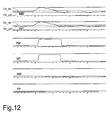
- the logic circuit 10 comprises a circuit 11 which comprises, in turn, as shown in figure 13 , two AND logic ports SEQ1 and SEQ2 having at the input the signals PM, MM, MP and PP and having at the output logic pulses PULSE_P and PULSE_N only if the sequence is that shown in figure 14 . Otherwise, if there is a disturbance, as shown in figure 12 , the output of the AND port SEQ1 remains zero.
- Discriminator 7 still preferably comprises control means adapted to set up a given time period TIME_WINDOW starting from the generation of the first pulse PULSE_P or PULSE_N of said other means; the control means are adapted to check whether within said time period the second pulse PULSE_N or PULSE_P is generated and are adapted to trigger said decoding means of the received signal only if the check result is positive.
- Circuit 11 is adapted to implement the control function on the time sequence of the logic signals. Indeed, the signals PULSE_P and PULSE_N are at the input of two latches P_LATCH and N_LATCH having at the output the signals P_L, P_L_NEG and N_L, N_L_NEG.
- the signals PULSE_P and PULSE_N are at the input of a NOR port POR_N, the output of which is at the input of another latch TW; the output Q of the latch TW is at the input of a delay cell DEL adapted to provide the time window TIME_WINDOW as the reset signal R of the latches TW, P_LATCH and N_LATCH. If a first couple of pulses between the pulses PM, MM, MP and PP meeting the described conditions comes, the time window TIME_WINDOW, the duration of which depends on the expected duration of the pulses, is started. If within such a time window the predicted couple of pulses comes, the clock signal and the data synchronous therewith is decoded.
- the clock and data recovery circuit 12 comprises an AND port CLOCKPULSE having at the input the signals P_L and N_L and the output of which is at the input of the latch CKFF providing the clock signal CLOCK; therefore, said clock signal CLOCK is decoded through the logic port CLOCKPULSE and the latch CKFF only if the two couples of pulses are correctly received.
- the discriminator 7 may have three filtering levels of disturbances: a hysteresis between the detection thresholds of the pulses within which the differential noise or the common-mode noise is ignored, the need for the first couple of pulses to come according to the sequence in figure 14 , the need for the second couple of pulses to come according to the sequence in figure 14 .
- time window TIME_WINDOW ensures that the system does not indefinitely keep on waiting for the second couple of pulses.
- the same device 12 allows the data to be decoded,
- the device 12 comprises an AND port DATA_HIGH having at the input the signals P_L and N_L_NEG and the output of which is at the input of the latch DATASET, the output Q of which is at the input of an AND port 122.
- the device 12 also comprises an AND port DATA_LOW having at the input the signals N_L and P_L_NEG and the output of which is at the input of the latch DATARESET, the output Q denied of which is at the input of the AND port 122.
- a further latch DATA_OUT has the output of the port 122 at the input D carrying the data at the output by means of the signal DATA-DECODED only if the clock signal CLOCK is present at the input, i.e. only if the clock signal CLOCK is decoded.
- a receiver 4 may be implemented, comprising the input stage coupled to the turn L2 and provided with the disturbance rejection circuit 6 or the circuit consisting of the circuital blocks 51, 53 and 54 and the decoder 70 of the known type for decoding the received signal, in accordance with the first embodiment of the invention.
- a receiver 4 may also be implemented, comprising the discriminator 7 in accordance with the second embodiment of the invention and preferably an amplifier of the known type 55 placed between the turn L2 and the input of the discriminator 7.
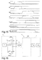
- a receiver 4 may also be implemented, in accordance with a third embodiment of the invention, comprising both the input stage 5, 50 coupled to the turn L2 and provided with the disturbance rejection circuit 6 or the circuit consisting of the circuital blocks 51, 53 and 54, as denoted in the first embodiment of the invention and its variations, and the discriminator 7, as denoted in the second embodiment of the invention, to obtain a more disturbance-immune receiver 4, as shown in figure 16 .
Landscapes
- Engineering & Computer Science (AREA)
- Computer Networks & Wireless Communication (AREA)
- Signal Processing (AREA)
- Power Engineering (AREA)
- Dc Digital Transmission (AREA)
- Amplifiers (AREA)
- Transceivers (AREA)
Applications Claiming Priority (1)
| Application Number | Priority Date | Filing Date | Title |
|---|---|---|---|
| ITMI20091382 | 2009-07-31 |
Publications (3)
| Publication Number | Publication Date |
|---|---|
| EP2282406A2 true EP2282406A2 (de) | 2011-02-09 |
| EP2282406A3 EP2282406A3 (de) | 2014-06-11 |
| EP2282406B1 EP2282406B1 (de) | 2016-04-20 |
Family
ID=41786446
Family Applications (1)
| Application Number | Title | Priority Date | Filing Date |
|---|---|---|---|
| EP10169807.4A Active EP2282406B1 (de) | 2009-07-31 | 2010-07-16 | Signalempfänger mit Störungsunterdrückung |
Country Status (1)
| Country | Link |
|---|---|
| EP (1) | EP2282406B1 (de) |
Cited By (1)
| Publication number | Priority date | Publication date | Assignee | Title |
|---|---|---|---|---|
| WO2017140884A1 (de) * | 2016-02-18 | 2017-08-24 | Elmos Semiconductor Aktiengesellschaft | Verfahren zur erhöhung des störabstands bei gleichtaktstörungen auf einem zweidrahtdatenbus |
Citations (2)
| Publication number | Priority date | Publication date | Assignee | Title |
|---|---|---|---|---|
| US20080069249A1 (en) | 2006-09-14 | 2008-03-20 | Stmicroelectronics S.A. | Transfer of digital data through a transformer |
| US20080311862A1 (en) | 2007-05-11 | 2008-12-18 | Stmicroelectronics S.R.L. | Integrated galvanic isolator using wireless transmission |
Family Cites Families (4)
| Publication number | Priority date | Publication date | Assignee | Title |
|---|---|---|---|---|
| US5252820A (en) * | 1991-03-11 | 1993-10-12 | Mitsubishi Denki Kabushiki Kaisha | Photoelectric conversion circuit having a tuning circuit and changeover switcher |
| US5568561A (en) * | 1993-04-22 | 1996-10-22 | Whitlock; William E. | Differential line receiver with common-mode AC bootstrapping |
| JP3931500B2 (ja) * | 1999-09-22 | 2007-06-13 | 松下電器産業株式会社 | 非接触icカードおよびそのデータ処理方法 |
| US6940466B2 (en) * | 2003-11-25 | 2005-09-06 | Starkey Laboratories, Inc. | Enhanced magnetic field communication system |
-
2010
- 2010-07-16 EP EP10169807.4A patent/EP2282406B1/de active Active
Patent Citations (2)
| Publication number | Priority date | Publication date | Assignee | Title |
|---|---|---|---|---|
| US20080069249A1 (en) | 2006-09-14 | 2008-03-20 | Stmicroelectronics S.A. | Transfer of digital data through a transformer |
| US20080311862A1 (en) | 2007-05-11 | 2008-12-18 | Stmicroelectronics S.R.L. | Integrated galvanic isolator using wireless transmission |
Cited By (2)
| Publication number | Priority date | Publication date | Assignee | Title |
|---|---|---|---|---|
| WO2017140884A1 (de) * | 2016-02-18 | 2017-08-24 | Elmos Semiconductor Aktiengesellschaft | Verfahren zur erhöhung des störabstands bei gleichtaktstörungen auf einem zweidrahtdatenbus |
| US10715362B2 (en) | 2016-02-18 | 2020-07-14 | Elmos Semiconductor Aktiengesellschaft | Method for increasing the signal-to-noise ratio for common-mode interference on a two-wire data bus |
Also Published As
| Publication number | Publication date |
|---|---|
| EP2282406A3 (de) | 2014-06-11 |
| EP2282406B1 (de) | 2016-04-20 |
Similar Documents
| Publication | Publication Date | Title |
|---|---|---|
| US8478332B2 (en) | Receiver for signal communication system with disturbance rejection circuit | |
| EP2282405B1 (de) | Signalkommunikationsvorrichtung und entsprechender Empfänger | |
| EP3291446A1 (de) | Galvanische isolierungsschaltung, entsprechendes system und verfahren | |
| US7639746B2 (en) | Hybrid voltage/current-mode transmission line driver | |
| US8451032B2 (en) | Capacitive isolator with schmitt trigger | |
| EP3512087A1 (de) | Galvanisch isolierter gleichspannungsschaltungswandler mit datenkommunikation, entsprechendes system und entsprechendes verfahren | |
| US9948193B2 (en) | Galvanically isolated DC-DC converter with bidirectional data transmission | |
| EP3386106B1 (de) | Empfängerschaltung | |
| US10637468B2 (en) | Galvanically-isolated signaling between modules with step-up transformer | |
| US8022762B2 (en) | Multi-stage CMOS power amplifier | |
| CN105429625A (zh) | 产生用于信号隔离器的通/断键控载波信号的方法和结构 | |
| CN109565480B (zh) | 具有改进的共模瞬态拒绝的电气隔离的数据隔离器 | |
| US20140062527A1 (en) | Isolation receiver | |
| EP3683964B1 (de) | Verfahren und strukturen zur erzeugung von codierten ein-/aus-trägersignalen für signalisolatoren | |
| CN103124187A (zh) | 具有单电源和低共模emi发射的3级桥式驱动器 | |
| EP2282406B1 (de) | Signalempfänger mit Störungsunterdrückung | |
| US20050258884A1 (en) | [dc level wandering cancellation circuit] | |
| US20110237206A1 (en) | Switched power amplifier topology providing high efficiency | |
| CN210807206U (zh) | 集成磁隔离芯片的边沿转换电路 | |
| US9847777B2 (en) | Signal potential converter | |
| WO2015055129A1 (zh) | 射频识别中的负载调制电路 | |
| US12249995B2 (en) | Differential interface circuit | |
| CN112313862B (zh) | 隔离驱动器 | |
| IT202300005733A1 (it) | Circuito di comunicazione, sistema e procedimento corrispondenti |
Legal Events
| Date | Code | Title | Description |
|---|---|---|---|
| PUAI | Public reference made under article 153(3) epc to a published international application that has entered the european phase |
Free format text: ORIGINAL CODE: 0009012 |
|
| AK | Designated contracting states |
Kind code of ref document: A2 Designated state(s): AL AT BE BG CH CY CZ DE DK EE ES FI FR GB GR HR HU IE IS IT LI LT LU LV MC MK MT NL NO PL PT RO SE SI SK SM TR |
|
| AX | Request for extension of the european patent |
Extension state: BA ME RS |
|
| RAP1 | Party data changed (applicant data changed or rights of an application transferred) |
Owner name: STMICROELECTRONICS SRL |
|
| PUAL | Search report despatched |
Free format text: ORIGINAL CODE: 0009013 |
|
| AK | Designated contracting states |
Kind code of ref document: A3 Designated state(s): AL AT BE BG CH CY CZ DE DK EE ES FI FR GB GR HR HU IE IS IT LI LT LU LV MC MK MT NL NO PL PT RO SE SI SK SM TR |
|
| AX | Request for extension of the european patent |
Extension state: BA ME RS |
|
| RIC1 | Information provided on ipc code assigned before grant |
Ipc: H04L 25/02 20060101ALI20140507BHEP Ipc: H04B 1/12 20060101AFI20140507BHEP |
|
| 17P | Request for examination filed |
Effective date: 20141023 |
|
| RBV | Designated contracting states (corrected) |
Designated state(s): AL AT BE BG CH CY CZ DE DK EE ES FI FR GB GR HR HU IE IS IT LI LT LU LV MC MK MT NL NO PL PT RO SE SI SK SM TR |
|
| GRAP | Despatch of communication of intention to grant a patent |
Free format text: ORIGINAL CODE: EPIDOSNIGR1 |
|
| INTG | Intention to grant announced |
Effective date: 20151203 |
|
| GRAS | Grant fee paid |
Free format text: ORIGINAL CODE: EPIDOSNIGR3 |
|
| GRAA | (expected) grant |
Free format text: ORIGINAL CODE: 0009210 |
|
| AK | Designated contracting states |
Kind code of ref document: B1 Designated state(s): AL AT BE BG CH CY CZ DE DK EE ES FI FR GB GR HR HU IE IS IT LI LT LU LV MC MK MT NL NO PL PT RO SE SI SK SM TR |
|
| REG | Reference to a national code |
Ref country code: GB Ref legal event code: FG4D |
|
| REG | Reference to a national code |
Ref country code: CH Ref legal event code: EP |
|
| REG | Reference to a national code |
Ref country code: AT Ref legal event code: REF Ref document number: 793429 Country of ref document: AT Kind code of ref document: T Effective date: 20160515 |
|
| REG | Reference to a national code |
Ref country code: IE Ref legal event code: FG4D |
|
| REG | Reference to a national code |
Ref country code: DE Ref legal event code: R096 Ref document number: 602010032409 Country of ref document: DE |
|
| REG | Reference to a national code |
Ref country code: FR Ref legal event code: PLFP Year of fee payment: 7 |
|
| REG | Reference to a national code |
Ref country code: LT Ref legal event code: MG4D |
|
| REG | Reference to a national code |
Ref country code: AT Ref legal event code: MK05 Ref document number: 793429 Country of ref document: AT Kind code of ref document: T Effective date: 20160420 |
|
| REG | Reference to a national code |
Ref country code: NL Ref legal event code: MP Effective date: 20160420 |
|
| PG25 | Lapsed in a contracting state [announced via postgrant information from national office to epo] |
Ref country code: FI Free format text: LAPSE BECAUSE OF FAILURE TO SUBMIT A TRANSLATION OF THE DESCRIPTION OR TO PAY THE FEE WITHIN THE PRESCRIBED TIME-LIMIT Effective date: 20160420 Ref country code: NL Free format text: LAPSE BECAUSE OF FAILURE TO SUBMIT A TRANSLATION OF THE DESCRIPTION OR TO PAY THE FEE WITHIN THE PRESCRIBED TIME-LIMIT Effective date: 20160420 Ref country code: LT Free format text: LAPSE BECAUSE OF FAILURE TO SUBMIT A TRANSLATION OF THE DESCRIPTION OR TO PAY THE FEE WITHIN THE PRESCRIBED TIME-LIMIT Effective date: 20160420 Ref country code: NO Free format text: LAPSE BECAUSE OF FAILURE TO SUBMIT A TRANSLATION OF THE DESCRIPTION OR TO PAY THE FEE WITHIN THE PRESCRIBED TIME-LIMIT Effective date: 20160720 Ref country code: PL Free format text: LAPSE BECAUSE OF FAILURE TO SUBMIT A TRANSLATION OF THE DESCRIPTION OR TO PAY THE FEE WITHIN THE PRESCRIBED TIME-LIMIT Effective date: 20160420 |
|
| PG25 | Lapsed in a contracting state [announced via postgrant information from national office to epo] |
Ref country code: GR Free format text: LAPSE BECAUSE OF FAILURE TO SUBMIT A TRANSLATION OF THE DESCRIPTION OR TO PAY THE FEE WITHIN THE PRESCRIBED TIME-LIMIT Effective date: 20160721 Ref country code: HR Free format text: LAPSE BECAUSE OF FAILURE TO SUBMIT A TRANSLATION OF THE DESCRIPTION OR TO PAY THE FEE WITHIN THE PRESCRIBED TIME-LIMIT Effective date: 20160420 Ref country code: AT Free format text: LAPSE BECAUSE OF FAILURE TO SUBMIT A TRANSLATION OF THE DESCRIPTION OR TO PAY THE FEE WITHIN THE PRESCRIBED TIME-LIMIT Effective date: 20160420 Ref country code: SE Free format text: LAPSE BECAUSE OF FAILURE TO SUBMIT A TRANSLATION OF THE DESCRIPTION OR TO PAY THE FEE WITHIN THE PRESCRIBED TIME-LIMIT Effective date: 20160420 Ref country code: LV Free format text: LAPSE BECAUSE OF FAILURE TO SUBMIT A TRANSLATION OF THE DESCRIPTION OR TO PAY THE FEE WITHIN THE PRESCRIBED TIME-LIMIT Effective date: 20160420 Ref country code: ES Free format text: LAPSE BECAUSE OF FAILURE TO SUBMIT A TRANSLATION OF THE DESCRIPTION OR TO PAY THE FEE WITHIN THE PRESCRIBED TIME-LIMIT Effective date: 20160420 Ref country code: PT Free format text: LAPSE BECAUSE OF FAILURE TO SUBMIT A TRANSLATION OF THE DESCRIPTION OR TO PAY THE FEE WITHIN THE PRESCRIBED TIME-LIMIT Effective date: 20160822 |
|
| PG25 | Lapsed in a contracting state [announced via postgrant information from national office to epo] |
Ref country code: IT Free format text: LAPSE BECAUSE OF FAILURE TO SUBMIT A TRANSLATION OF THE DESCRIPTION OR TO PAY THE FEE WITHIN THE PRESCRIBED TIME-LIMIT Effective date: 20160420 Ref country code: BE Free format text: LAPSE BECAUSE OF FAILURE TO SUBMIT A TRANSLATION OF THE DESCRIPTION OR TO PAY THE FEE WITHIN THE PRESCRIBED TIME-LIMIT Effective date: 20160420 |
|
| REG | Reference to a national code |
Ref country code: DE Ref legal event code: R097 Ref document number: 602010032409 Country of ref document: DE |
|
| PG25 | Lapsed in a contracting state [announced via postgrant information from national office to epo] |
Ref country code: RO Free format text: LAPSE BECAUSE OF FAILURE TO SUBMIT A TRANSLATION OF THE DESCRIPTION OR TO PAY THE FEE WITHIN THE PRESCRIBED TIME-LIMIT Effective date: 20160420 Ref country code: DK Free format text: LAPSE BECAUSE OF FAILURE TO SUBMIT A TRANSLATION OF THE DESCRIPTION OR TO PAY THE FEE WITHIN THE PRESCRIBED TIME-LIMIT Effective date: 20160420 Ref country code: SK Free format text: LAPSE BECAUSE OF FAILURE TO SUBMIT A TRANSLATION OF THE DESCRIPTION OR TO PAY THE FEE WITHIN THE PRESCRIBED TIME-LIMIT Effective date: 20160420 Ref country code: EE Free format text: LAPSE BECAUSE OF FAILURE TO SUBMIT A TRANSLATION OF THE DESCRIPTION OR TO PAY THE FEE WITHIN THE PRESCRIBED TIME-LIMIT Effective date: 20160420 Ref country code: CZ Free format text: LAPSE BECAUSE OF FAILURE TO SUBMIT A TRANSLATION OF THE DESCRIPTION OR TO PAY THE FEE WITHIN THE PRESCRIBED TIME-LIMIT Effective date: 20160420 |
|
| PLBE | No opposition filed within time limit |
Free format text: ORIGINAL CODE: 0009261 |
|
| STAA | Information on the status of an ep patent application or granted ep patent |
Free format text: STATUS: NO OPPOSITION FILED WITHIN TIME LIMIT |
|
| PG25 | Lapsed in a contracting state [announced via postgrant information from national office to epo] |
Ref country code: SM Free format text: LAPSE BECAUSE OF FAILURE TO SUBMIT A TRANSLATION OF THE DESCRIPTION OR TO PAY THE FEE WITHIN THE PRESCRIBED TIME-LIMIT Effective date: 20160420 |
|
| REG | Reference to a national code |
Ref country code: CH Ref legal event code: PL |
|
| GBPC | Gb: european patent ceased through non-payment of renewal fee |
Effective date: 20160720 |
|
| 26N | No opposition filed |
Effective date: 20170123 |
|
| PG25 | Lapsed in a contracting state [announced via postgrant information from national office to epo] |
Ref country code: MC Free format text: LAPSE BECAUSE OF FAILURE TO SUBMIT A TRANSLATION OF THE DESCRIPTION OR TO PAY THE FEE WITHIN THE PRESCRIBED TIME-LIMIT Effective date: 20160420 |
|
| PG25 | Lapsed in a contracting state [announced via postgrant information from national office to epo] |
Ref country code: CH Free format text: LAPSE BECAUSE OF NON-PAYMENT OF DUE FEES Effective date: 20160731 Ref country code: LI Free format text: LAPSE BECAUSE OF NON-PAYMENT OF DUE FEES Effective date: 20160731 |
|
| REG | Reference to a national code |
Ref country code: IE Ref legal event code: MM4A |
|
| PG25 | Lapsed in a contracting state [announced via postgrant information from national office to epo] |
Ref country code: GB Free format text: LAPSE BECAUSE OF NON-PAYMENT OF DUE FEES Effective date: 20160720 Ref country code: SI Free format text: LAPSE BECAUSE OF FAILURE TO SUBMIT A TRANSLATION OF THE DESCRIPTION OR TO PAY THE FEE WITHIN THE PRESCRIBED TIME-LIMIT Effective date: 20160420 |
|
| REG | Reference to a national code |
Ref country code: FR Ref legal event code: PLFP Year of fee payment: 8 |
|
| PG25 | Lapsed in a contracting state [announced via postgrant information from national office to epo] |
Ref country code: IE Free format text: LAPSE BECAUSE OF NON-PAYMENT OF DUE FEES Effective date: 20160716 |
|
| PG25 | Lapsed in a contracting state [announced via postgrant information from national office to epo] |
Ref country code: LU Free format text: LAPSE BECAUSE OF NON-PAYMENT OF DUE FEES Effective date: 20160716 |
|
| PG25 | Lapsed in a contracting state [announced via postgrant information from national office to epo] |
Ref country code: CY Free format text: LAPSE BECAUSE OF FAILURE TO SUBMIT A TRANSLATION OF THE DESCRIPTION OR TO PAY THE FEE WITHIN THE PRESCRIBED TIME-LIMIT Effective date: 20160420 Ref country code: HU Free format text: LAPSE BECAUSE OF FAILURE TO SUBMIT A TRANSLATION OF THE DESCRIPTION OR TO PAY THE FEE WITHIN THE PRESCRIBED TIME-LIMIT; INVALID AB INITIO Effective date: 20100716 |
|
| REG | Reference to a national code |
Ref country code: FR Ref legal event code: PLFP Year of fee payment: 9 |
|
| PG25 | Lapsed in a contracting state [announced via postgrant information from national office to epo] |
Ref country code: MK Free format text: LAPSE BECAUSE OF FAILURE TO SUBMIT A TRANSLATION OF THE DESCRIPTION OR TO PAY THE FEE WITHIN THE PRESCRIBED TIME-LIMIT Effective date: 20160420 Ref country code: IS Free format text: LAPSE BECAUSE OF FAILURE TO SUBMIT A TRANSLATION OF THE DESCRIPTION OR TO PAY THE FEE WITHIN THE PRESCRIBED TIME-LIMIT Effective date: 20160420 Ref country code: TR Free format text: LAPSE BECAUSE OF FAILURE TO SUBMIT A TRANSLATION OF THE DESCRIPTION OR TO PAY THE FEE WITHIN THE PRESCRIBED TIME-LIMIT Effective date: 20160420 Ref country code: MT Free format text: LAPSE BECAUSE OF NON-PAYMENT OF DUE FEES Effective date: 20160731 |
|
| PG25 | Lapsed in a contracting state [announced via postgrant information from national office to epo] |
Ref country code: BG Free format text: LAPSE BECAUSE OF FAILURE TO SUBMIT A TRANSLATION OF THE DESCRIPTION OR TO PAY THE FEE WITHIN THE PRESCRIBED TIME-LIMIT Effective date: 20160420 |
|
| PG25 | Lapsed in a contracting state [announced via postgrant information from national office to epo] |
Ref country code: AL Free format text: LAPSE BECAUSE OF FAILURE TO SUBMIT A TRANSLATION OF THE DESCRIPTION OR TO PAY THE FEE WITHIN THE PRESCRIBED TIME-LIMIT Effective date: 20160420 |
|
| PGFP | Annual fee paid to national office [announced via postgrant information from national office to epo] |
Ref country code: FR Payment date: 20200623 Year of fee payment: 11 |
|
| PG25 | Lapsed in a contracting state [announced via postgrant information from national office to epo] |
Ref country code: FR Free format text: LAPSE BECAUSE OF NON-PAYMENT OF DUE FEES Effective date: 20210731 |
|
| PGFP | Annual fee paid to national office [announced via postgrant information from national office to epo] |
Ref country code: DE Payment date: 20250620 Year of fee payment: 16 |