EP2281318B1 - Electronic device - Google Patents
Electronic device Download PDFInfo
- Publication number
- EP2281318B1 EP2281318B1 EP09753523.1A EP09753523A EP2281318B1 EP 2281318 B1 EP2281318 B1 EP 2281318B1 EP 09753523 A EP09753523 A EP 09753523A EP 2281318 B1 EP2281318 B1 EP 2281318B1
- Authority
- EP
- European Patent Office
- Prior art keywords
- matrix material
- electronic device
- homo
- lumo
- matrix
- Prior art date
- Legal status (The legal status is an assumption and is not a legal conclusion. Google has not performed a legal analysis and makes no representation as to the accuracy of the status listed.)
- Active
Links
- 239000011159 matrix material Substances 0.000 claims description 157
- 239000010410 layer Substances 0.000 claims description 97
- 239000000463 material Substances 0.000 claims description 67
- 238000004770 highest occupied molecular orbital Methods 0.000 claims description 61
- 238000004768 lowest unoccupied molecular orbital Methods 0.000 claims description 58
- 239000002800 charge carrier Substances 0.000 claims description 42
- 239000002346 layers by function Substances 0.000 claims description 28
- 230000037230 mobility Effects 0.000 claims description 25
- 230000005525 hole transport Effects 0.000 claims description 20
- 238000000034 method Methods 0.000 claims description 10
- 238000002347 injection Methods 0.000 claims description 9
- 239000007924 injection Substances 0.000 claims description 9
- 239000000758 substrate Substances 0.000 claims description 8
- 230000000903 blocking effect Effects 0.000 claims description 6
- 238000004519 manufacturing process Methods 0.000 claims description 6
- 230000008021 deposition Effects 0.000 claims description 2
- AWXGSYPUMWKTBR-UHFFFAOYSA-N 4-carbazol-9-yl-n,n-bis(4-carbazol-9-ylphenyl)aniline Chemical compound C12=CC=CC=C2C2=CC=CC=C2N1C1=CC=C(N(C=2C=CC(=CC=2)N2C3=CC=CC=C3C3=CC=CC=C32)C=2C=CC(=CC=2)N2C3=CC=CC=C3C3=CC=CC=C32)C=C1 AWXGSYPUMWKTBR-UHFFFAOYSA-N 0.000 description 7
- 239000007983 Tris buffer Substances 0.000 description 7
- 238000005215 recombination Methods 0.000 description 7
- 230000006798 recombination Effects 0.000 description 7
- YYMBJDOZVAITBP-UHFFFAOYSA-N rubrene Chemical compound C1=CC=CC=C1C(C1=C(C=2C=CC=CC=2)C2=CC=CC=C2C(C=2C=CC=CC=2)=C11)=C(C=CC=C2)C2=C1C1=CC=CC=C1 YYMBJDOZVAITBP-UHFFFAOYSA-N 0.000 description 7
- -1 transport Substances 0.000 description 7
- 101000837344 Homo sapiens T-cell leukemia translocation-altered gene protein Proteins 0.000 description 6
- 102100028692 T-cell leukemia translocation-altered gene protein Human genes 0.000 description 6
- 238000007740 vapor deposition Methods 0.000 description 5
- UJOBWOGCFQCDNV-UHFFFAOYSA-N 9H-carbazole Chemical compound C1=CC=C2C3=CC=CC=C3NC2=C1 UJOBWOGCFQCDNV-UHFFFAOYSA-N 0.000 description 4
- 230000007423 decrease Effects 0.000 description 4
- CECAIMUJVYQLKA-UHFFFAOYSA-N iridium 1-phenylisoquinoline Chemical compound [Ir].C1=CC=CC=C1C1=NC=CC2=CC=CC=C12.C1=CC=CC=C1C1=NC=CC2=CC=CC=C12.C1=CC=CC=C1C1=NC=CC2=CC=CC=C12 CECAIMUJVYQLKA-UHFFFAOYSA-N 0.000 description 4
- UEEXRMUCXBPYOV-UHFFFAOYSA-N iridium;2-phenylpyridine Chemical compound [Ir].C1=CC=CC=C1C1=CC=CC=N1.C1=CC=CC=C1C1=CC=CC=N1.C1=CC=CC=C1C1=CC=CC=N1 UEEXRMUCXBPYOV-UHFFFAOYSA-N 0.000 description 4
- 238000004776 molecular orbital Methods 0.000 description 4
- 239000012044 organic layer Substances 0.000 description 4
- 238000004088 simulation Methods 0.000 description 4
- 239000002019 doping agent Substances 0.000 description 3
- 230000005284 excitation Effects 0.000 description 3
- 238000001420 photoelectron spectroscopy Methods 0.000 description 3
- XSVXWCZFSFKRDO-UHFFFAOYSA-N triphenyl-(3-triphenylsilylphenyl)silane Chemical compound C1=CC=CC=C1[Si](C=1C=C(C=CC=1)[Si](C=1C=CC=CC=1)(C=1C=CC=CC=1)C=1C=CC=CC=1)(C=1C=CC=CC=1)C1=CC=CC=C1 XSVXWCZFSFKRDO-UHFFFAOYSA-N 0.000 description 3
- DETFWTCLAIIJRZ-UHFFFAOYSA-N triphenyl-(4-triphenylsilylphenyl)silane Chemical compound C1=CC=CC=C1[Si](C=1C=CC(=CC=1)[Si](C=1C=CC=CC=1)(C=1C=CC=CC=1)C=1C=CC=CC=1)(C=1C=CC=CC=1)C1=CC=CC=C1 DETFWTCLAIIJRZ-UHFFFAOYSA-N 0.000 description 3
- POILWHVDKZOXJZ-ARJAWSKDSA-M (z)-4-oxopent-2-en-2-olate Chemical compound C\C([O-])=C\C(C)=O POILWHVDKZOXJZ-ARJAWSKDSA-M 0.000 description 2
- MQRCTQVBZYBPQE-UHFFFAOYSA-N 189363-47-1 Chemical compound C1=CC=CC=C1N(C=1C=C2C3(C4=CC(=CC=C4C2=CC=1)N(C=1C=CC=CC=1)C=1C=CC=CC=1)C1=CC(=CC=C1C1=CC=C(C=C13)N(C=1C=CC=CC=1)C=1C=CC=CC=1)N(C=1C=CC=CC=1)C=1C=CC=CC=1)C1=CC=CC=C1 MQRCTQVBZYBPQE-UHFFFAOYSA-N 0.000 description 2
- OBAJPWYDYFEBTF-UHFFFAOYSA-N 2-tert-butyl-9,10-dinaphthalen-2-ylanthracene Chemical compound C1=CC=CC2=CC(C3=C4C=CC=CC4=C(C=4C=C5C=CC=CC5=CC=4)C4=CC=C(C=C43)C(C)(C)C)=CC=C21 OBAJPWYDYFEBTF-UHFFFAOYSA-N 0.000 description 2
- ZVFQEOPUXVPSLB-UHFFFAOYSA-N 3-(4-tert-butylphenyl)-4-phenyl-5-(4-phenylphenyl)-1,2,4-triazole Chemical compound C1=CC(C(C)(C)C)=CC=C1C(N1C=2C=CC=CC=2)=NN=C1C1=CC=C(C=2C=CC=CC=2)C=C1 ZVFQEOPUXVPSLB-UHFFFAOYSA-N 0.000 description 2
- ZOKIJILZFXPFTO-UHFFFAOYSA-N 4-methyl-n-[4-[1-[4-(4-methyl-n-(4-methylphenyl)anilino)phenyl]cyclohexyl]phenyl]-n-(4-methylphenyl)aniline Chemical compound C1=CC(C)=CC=C1N(C=1C=CC(=CC=1)C1(CCCCC1)C=1C=CC(=CC=1)N(C=1C=CC(C)=CC=1)C=1C=CC(C)=CC=1)C1=CC=C(C)C=C1 ZOKIJILZFXPFTO-UHFFFAOYSA-N 0.000 description 2
- AOQKGYRILLEVJV-UHFFFAOYSA-N 4-naphthalen-1-yl-3,5-diphenyl-1,2,4-triazole Chemical compound C1=CC=CC=C1C(N1C=2C3=CC=CC=C3C=CC=2)=NN=C1C1=CC=CC=C1 AOQKGYRILLEVJV-UHFFFAOYSA-N 0.000 description 2
- VIJYEGDOKCKUOL-UHFFFAOYSA-N 9-phenylcarbazole Chemical compound C1=CC=CC=C1N1C2=CC=CC=C2C2=CC=CC=C21 VIJYEGDOKCKUOL-UHFFFAOYSA-N 0.000 description 2
- 238000010521 absorption reaction Methods 0.000 description 2
- XAGFODPZIPBFFR-UHFFFAOYSA-N aluminium Chemical compound [Al] XAGFODPZIPBFFR-UHFFFAOYSA-N 0.000 description 2
- 229910052782 aluminium Inorganic materials 0.000 description 2
- 238000002484 cyclic voltammetry Methods 0.000 description 2
- 238000010586 diagram Methods 0.000 description 2
- ZUOUZKKEUPVFJK-UHFFFAOYSA-N diphenyl Chemical compound C1=CC=CC=C1C1=CC=CC=C1 ZUOUZKKEUPVFJK-UHFFFAOYSA-N 0.000 description 2
- 230000008020 evaporation Effects 0.000 description 2
- 238000001704 evaporation Methods 0.000 description 2
- HQSLHDHQIQJZHQ-UHFFFAOYSA-N 1,2,3,4-tetraphenyltetracene Chemical compound C1=CC=CC=C1C(C(=C1C=C2C=C3C=CC=CC3=CC2=CC1=C1C=2C=CC=CC=2)C=2C=CC=CC=2)=C1C1=CC=CC=C1 HQSLHDHQIQJZHQ-UHFFFAOYSA-N 0.000 description 1
- XNCMQRWVMWLODV-UHFFFAOYSA-N 1-phenylbenzimidazole Chemical compound C1=NC2=CC=CC=C2N1C1=CC=CC=C1 XNCMQRWVMWLODV-UHFFFAOYSA-N 0.000 description 1
- STTGYIUESPWXOW-UHFFFAOYSA-N 2,9-dimethyl-4,7-diphenyl-1,10-phenanthroline Chemical compound C=12C=CC3=C(C=4C=CC=CC=4)C=C(C)N=C3C2=NC(C)=CC=1C1=CC=CC=C1 STTGYIUESPWXOW-UHFFFAOYSA-N 0.000 description 1
- NBYLBWHHTUWMER-UHFFFAOYSA-N 2-Methylquinolin-8-ol Chemical compound C1=CC=C(O)C2=NC(C)=CC=C21 NBYLBWHHTUWMER-UHFFFAOYSA-N 0.000 description 1
- MTUBTKOZCCGPSU-UHFFFAOYSA-N 2-n-naphthalen-1-yl-1-n,1-n,2-n-triphenylbenzene-1,2-diamine Chemical compound C1=CC=CC=C1N(C=1C(=CC=CC=1)N(C=1C=CC=CC=1)C=1C2=CC=CC=C2C=CC=1)C1=CC=CC=C1 MTUBTKOZCCGPSU-UHFFFAOYSA-N 0.000 description 1
- DHDHJYNTEFLIHY-UHFFFAOYSA-N 4,7-diphenyl-1,10-phenanthroline Chemical compound C1=CC=CC=C1C1=CC=NC2=C1C=CC1=C(C=3C=CC=CC=3)C=CN=C21 DHDHJYNTEFLIHY-UHFFFAOYSA-N 0.000 description 1
- OSQXTXTYKAEHQV-WXUKJITCSA-N 4-methyl-n-[4-[(e)-2-[4-[4-[(e)-2-[4-(4-methyl-n-(4-methylphenyl)anilino)phenyl]ethenyl]phenyl]phenyl]ethenyl]phenyl]-n-(4-methylphenyl)aniline Chemical compound C1=CC(C)=CC=C1N(C=1C=CC(\C=C\C=2C=CC(=CC=2)C=2C=CC(\C=C\C=3C=CC(=CC=3)N(C=3C=CC(C)=CC=3)C=3C=CC(C)=CC=3)=CC=2)=CC=1)C1=CC=C(C)C=C1 OSQXTXTYKAEHQV-WXUKJITCSA-N 0.000 description 1
- CRHRWHRNQKPUPO-UHFFFAOYSA-N 4-n-naphthalen-1-yl-1-n,1-n-bis[4-(n-naphthalen-1-ylanilino)phenyl]-4-n-phenylbenzene-1,4-diamine Chemical compound C1=CC=CC=C1N(C=1C2=CC=CC=C2C=CC=1)C1=CC=C(N(C=2C=CC(=CC=2)N(C=2C=CC=CC=2)C=2C3=CC=CC=C3C=CC=2)C=2C=CC(=CC=2)N(C=2C=CC=CC=2)C=2C3=CC=CC=C3C=CC=2)C=C1 CRHRWHRNQKPUPO-UHFFFAOYSA-N 0.000 description 1
- MZYDBGLUVPLRKR-UHFFFAOYSA-N 9-(3-carbazol-9-ylphenyl)carbazole Chemical compound C12=CC=CC=C2C2=CC=CC=C2N1C1=CC(N2C3=CC=CC=C3C3=CC=CC=C32)=CC=C1 MZYDBGLUVPLRKR-UHFFFAOYSA-N 0.000 description 1
- RAPHUPWIHDYTKU-WXUKJITCSA-N 9-ethyl-3-[(e)-2-[4-[4-[(e)-2-(9-ethylcarbazol-3-yl)ethenyl]phenyl]phenyl]ethenyl]carbazole Chemical compound C1=CC=C2C3=CC(/C=C/C4=CC=C(C=C4)C4=CC=C(C=C4)/C=C/C=4C=C5C6=CC=CC=C6N(C5=CC=4)CC)=CC=C3N(CC)C2=C1 RAPHUPWIHDYTKU-WXUKJITCSA-N 0.000 description 1
- MVMBITSRQNHOLP-UHFFFAOYSA-N OC(=O)C1=NC=CC=C1[Ir]C1=CC(F)=CC(F)=C1C1=CC=CC=N1 Chemical compound OC(=O)C1=NC=CC=C1[Ir]C1=CC(F)=CC(F)=C1C1=CC=CC=N1 MVMBITSRQNHOLP-UHFFFAOYSA-N 0.000 description 1
- VYVIOMJSKUGJLV-UHFFFAOYSA-N [Ir+2] Chemical compound [Ir+2] VYVIOMJSKUGJLV-UHFFFAOYSA-N 0.000 description 1
- NFNALQOLQWJCNE-UHFFFAOYSA-N [Ir+3].C1=CC=C2C3=NC(C)=CN=C3C3=CC=CC=C3C2=C1.C1=CC=C2C3=NC(C)=CN=C3C3=CC=CC=C3C2=C1 Chemical compound [Ir+3].C1=CC=C2C3=NC(C)=CN=C3C3=CC=CC=C3C2=C1.C1=CC=C2C3=NC(C)=CN=C3C3=CC=CC=C3C2=C1 NFNALQOLQWJCNE-UHFFFAOYSA-N 0.000 description 1
- IEVQFYKGWUDNTF-UHFFFAOYSA-M [O-]C(C1=NC=CC=C1[Ir+]C1=CC(F)=CC(F)=C1C1=CC=CC=N1)=O Chemical compound [O-]C(C1=NC=CC=C1[Ir+]C1=CC(F)=CC(F)=C1C1=CC=CC=N1)=O IEVQFYKGWUDNTF-UHFFFAOYSA-M 0.000 description 1
- 238000005263 ab initio calculation Methods 0.000 description 1
- CUJRVFIICFDLGR-UHFFFAOYSA-N acetylacetonate Chemical compound CC(=O)[CH-]C(C)=O CUJRVFIICFDLGR-UHFFFAOYSA-N 0.000 description 1
- 230000004913 activation Effects 0.000 description 1
- 230000004888 barrier function Effects 0.000 description 1
- 235000010290 biphenyl Nutrition 0.000 description 1
- 239000004305 biphenyl Substances 0.000 description 1
- UFVXQDWNSAGPHN-UHFFFAOYSA-K bis[(2-methylquinolin-8-yl)oxy]-(4-phenylphenoxy)alumane Chemical compound [Al+3].C1=CC=C([O-])C2=NC(C)=CC=C21.C1=CC=C([O-])C2=NC(C)=CC=C21.C1=CC([O-])=CC=C1C1=CC=CC=C1 UFVXQDWNSAGPHN-UHFFFAOYSA-K 0.000 description 1
- 125000004556 carbazol-9-yl group Chemical group C1=CC=CC=2C3=CC=CC=C3N(C12)* 0.000 description 1
- 239000000969 carrier Substances 0.000 description 1
- 230000015556 catabolic process Effects 0.000 description 1
- 230000008859 change Effects 0.000 description 1
- XCJYREBRNVKWGJ-UHFFFAOYSA-N copper(II) phthalocyanine Chemical compound [Cu+2].C12=CC=CC=C2C(N=C2[N-]C(C3=CC=CC=C32)=N2)=NC1=NC([C]1C=CC=CC1=1)=NC=1N=C1[C]3C=CC=CC3=C2[N-]1 XCJYREBRNVKWGJ-UHFFFAOYSA-N 0.000 description 1
- 230000008878 coupling Effects 0.000 description 1
- 238000010168 coupling process Methods 0.000 description 1
- 238000005859 coupling reaction Methods 0.000 description 1
- 239000013078 crystal Substances 0.000 description 1
- 238000006731 degradation reaction Methods 0.000 description 1
- 230000001419 dependent effect Effects 0.000 description 1
- 230000005281 excited state Effects 0.000 description 1
- 230000002349 favourable effect Effects 0.000 description 1
- 238000002189 fluorescence spectrum Methods 0.000 description 1
- 229910052741 iridium Inorganic materials 0.000 description 1
- GKOZUEZYRPOHIO-UHFFFAOYSA-N iridium atom Chemical compound [Ir] GKOZUEZYRPOHIO-UHFFFAOYSA-N 0.000 description 1
- 239000000203 mixture Substances 0.000 description 1
- YPJRZWDWVBNDIW-MBALSZOMSA-N n,n-diphenyl-4-[(e)-2-[4-[4-[(e)-2-[4-(n-phenylanilino)phenyl]ethenyl]phenyl]phenyl]ethenyl]aniline Chemical group C=1C=C(N(C=2C=CC=CC=2)C=2C=CC=CC=2)C=CC=1/C=C/C(C=C1)=CC=C1C(C=C1)=CC=C1\C=C\C(C=C1)=CC=C1N(C=1C=CC=CC=1)C1=CC=CC=C1 YPJRZWDWVBNDIW-MBALSZOMSA-N 0.000 description 1
- DCZNSJVFOQPSRV-UHFFFAOYSA-N n,n-diphenyl-4-[4-(n-phenylanilino)phenyl]aniline Chemical compound C1=CC=CC=C1N(C=1C=CC(=CC=1)C=1C=CC(=CC=1)N(C=1C=CC=CC=1)C=1C=CC=CC=1)C1=CC=CC=C1 DCZNSJVFOQPSRV-UHFFFAOYSA-N 0.000 description 1
- IBHBKWKFFTZAHE-UHFFFAOYSA-N n-[4-[4-(n-naphthalen-1-ylanilino)phenyl]phenyl]-n-phenylnaphthalen-1-amine Chemical compound C1=CC=CC=C1N(C=1C2=CC=CC=C2C=CC=1)C1=CC=C(C=2C=CC(=CC=2)N(C=2C=CC=CC=2)C=2C3=CC=CC=C3C=CC=2)C=C1 IBHBKWKFFTZAHE-UHFFFAOYSA-N 0.000 description 1
- 230000005693 optoelectronics Effects 0.000 description 1
- 238000004838 photoelectron emission spectroscopy Methods 0.000 description 1
- VVOPUZNLRVJDJQ-UHFFFAOYSA-N phthalocyanine copper Chemical compound [Cu].C12=CC=CC=C2C(N=C2NC(C3=CC=CC=C32)=N2)=NC1=NC([C]1C=CC=CC1=1)=NC=1N=C1[C]3C=CC=CC3=C2N1 VVOPUZNLRVJDJQ-UHFFFAOYSA-N 0.000 description 1
- 229920000642 polymer Polymers 0.000 description 1
- 239000010453 quartz Substances 0.000 description 1
- 238000010791 quenching Methods 0.000 description 1
- 230000000171 quenching effect Effects 0.000 description 1
- 230000005855 radiation Effects 0.000 description 1
- VYPSYNLAJGMNEJ-UHFFFAOYSA-N silicon dioxide Inorganic materials O=[Si]=O VYPSYNLAJGMNEJ-UHFFFAOYSA-N 0.000 description 1
- 150000003384 small molecules Chemical class 0.000 description 1
- 239000007787 solid Substances 0.000 description 1
- 238000004611 spectroscopical analysis Methods 0.000 description 1
- 239000000126 substance Substances 0.000 description 1
- 230000007704 transition Effects 0.000 description 1
- LENZDBCJOHFCAS-UHFFFAOYSA-N tris Chemical compound OCC(N)(CO)CO LENZDBCJOHFCAS-UHFFFAOYSA-N 0.000 description 1
- 230000005428 wave function Effects 0.000 description 1
Images


Classifications
-
- H—ELECTRICITY
- H10—SEMICONDUCTOR DEVICES; ELECTRIC SOLID-STATE DEVICES NOT OTHERWISE PROVIDED FOR
- H10K—ORGANIC ELECTRIC SOLID-STATE DEVICES
- H10K50/00—Organic light-emitting devices
- H10K50/10—OLEDs or polymer light-emitting diodes [PLED]
- H10K50/11—OLEDs or polymer light-emitting diodes [PLED] characterised by the electroluminescent [EL] layers
-
- H—ELECTRICITY
- H10—SEMICONDUCTOR DEVICES; ELECTRIC SOLID-STATE DEVICES NOT OTHERWISE PROVIDED FOR
- H10K—ORGANIC ELECTRIC SOLID-STATE DEVICES
- H10K50/00—Organic light-emitting devices
- H10K50/10—OLEDs or polymer light-emitting diodes [PLED]
- H10K50/14—Carrier transporting layers
-
- H—ELECTRICITY
- H10—SEMICONDUCTOR DEVICES; ELECTRIC SOLID-STATE DEVICES NOT OTHERWISE PROVIDED FOR
- H10K—ORGANIC ELECTRIC SOLID-STATE DEVICES
- H10K2101/00—Properties of the organic materials covered by group H10K85/00
- H10K2101/30—Highest occupied molecular orbital [HOMO], lowest unoccupied molecular orbital [LUMO] or Fermi energy values
-
- H—ELECTRICITY
- H10—SEMICONDUCTOR DEVICES; ELECTRIC SOLID-STATE DEVICES NOT OTHERWISE PROVIDED FOR
- H10K—ORGANIC ELECTRIC SOLID-STATE DEVICES
- H10K2101/00—Properties of the organic materials covered by group H10K85/00
- H10K2101/90—Multiple hosts in the emissive layer
Definitions
- the invention relates to an electronic device and a method for producing an electronic device.
- OLEDs organic light emitting diodes
- Emission layers in this case have a matrix material which is doped with emitter molecules.
- excitons are formed by recombination of electrons and "holes” that lead to light emission.
- the ratio between electrons and "holes" transported in the emission layer is crucial. An unbalanced relationship between hole and electron transport results in low radiation efficiency of the device.
- the publication US 2008/0116536 relates to a photosensitive optoelectronic device.
- the document US 2006/068223 describes a doped oleb having multiple host materials.
- the object of the invention is to provide an electronic device which has an improved charge carrier transport and an improved charge carrier balance in the organic layers and thus an increased Efficiency.
- Another object of the invention is to provide a method of manufacturing an electronic device. These tasks are through An electronic device according to claim 1 and a method for manufacturing the electronic device according to claim 12. Further embodiments of the device and the method are the subject of further claims.
- an electronic device which comprises a substrate, a first electrode, at least one organic, functional layer and a second electrode, wherein the at least one organic functional layer is arranged between the first electrode and the second electrode.
- the first electrode may be arranged on the substrate, the at least one organic functional layer on the first electrode, and the second electrode on the at least one organic, functional layer.
- the at least one organic functional layer comprises at least a first matrix material, a second matrix material and a third matrix material, wherein the third matrix material is a Lowest Unoccupied Molecular Orbital (LUMO) which is lower in energy than the LUMO of the second matrix material and the LUMO of the first matrix material and wherein the second matrix material is a Highest Occupied Molecular Orbital (HOMO) that is higher in energy than the HOMO of the first matrix material and the HOMO of the third matrix material.
- the at least one organic, functional layer is an emission layer and doped with at least one emitter material.
- This provides an electronic device comprising more than two different matrix materials in an organic functional layer. There may be three different matrix materials, and more than three as needed.
- the molecular orbital theory in a molecule are different molecular orbitals with different energy levels present, which can be occupied by the existing electrons. These molecular orbitals are occupied according to increasing energy levels.
- the LUMO is the lowest energy molecular orbital that is no longer occupied by an electron.
- the HOMO is the highest molecular orbital in terms of energy, which is still occupied by an electron.
- This electronic device has improved charge carrier transport and carrier balance in the organic functional layer, and an adaptable hole-to-electron transport relationship.
- the first matrix material is chosen such that it has a large band gap, ie the difference between HOMO and LUMO, for example so that its HOMO lies energetically below the HOMO of the other two matrix materials and its LUMO energetically above the LUMO of the other two matrix materials.
- the first matrix material may have a LUMO that is higher in energy than the LUMO of the second matrix material and the LUMO of the third matrix material, and a HOMO that is lower in energy than the HOMO of the second matrix material and the HOMO of the third matrix material.
- the second matrix material may have a LUMO higher in energy than the LUMO of the third matrix material and a HOMO higher in energy than the HOMO of the third matrix material.
- the first matrix material may have the largest band gap between HOMO and LUMO compared to the second and the third matrix material and the second matrix material has a bandgap which is energetically shifted to the bandgap of the third matrix material.
- electrons can be transported on the LUMO of the third matrix material, and holes can be transported on the HOMO of the second matrix material, since these energy levels are the most energetically favorable for the respective charge transport.
- the first matrix material may have in the electronic device a charge carrier mobility that is less than the charge carrier mobility of the second and the third matrix material.
- the first matrix material may be an Ultra Wide Band Gap (UGH) material which has a large band gap compared to the other matrix materials. As a result, it can not have any share in the transport of charge carriers.
- UMW Ultra Wide Band Gap
- the second matrix material may further comprise a hole transport material and the third matrix material may comprise an electron transport material.
- the charge carrier transport ie the hole transport and the electron transport, depends in particular on the mobility of the holes or the electrons in a material and on the location of the energy levels HOMO and LUMO of the matrix materials.
- the HOMO and LUMO of a material is responsible for the charge carrier injection.
- the second one Matrix material having a HOMO higher than the third matrix material better suited as a hole transport material than the third matrix material.
- the third matrix material having a lower LUMO than the second matrix material is suitable as an electron transport material.
- a matrix material may serve as an electron transport material or as a hole transport material.
- the charge carrier transport of the other charge takes place, but it predominates the transport of a charge carrier. If no charge carrier transport takes place in a matrix material, as in one embodiment of the invention in the first matrix material, this can either be due to the fact that no charge carriers are generated or that there is no mobility of the charge carriers.
- further matrix materials may be present in the organic, functional layer that do not contribute to the charge carrier transport.
- the energy levels HOMO and LUMO of a material can be measured to select suitable materials for first, second and third matrix materials.
- the HOMO of a material can be determined by cyclic voltammetry.
- the band gap, ie the energetic difference between HOMO and LUMO, can still be determined by means of spectroscopy, in which the wavelength of the emitted light is measured and from this the resulting excitons and the band gap is calculated.
- the energy level of the LUMO is then calculated from the determined HOMO and the bandgap.
- the HOMO can alternatively be determined by means of photoelectron spectroscopy.
- the mobility of electrons and holes may depend on the molecular distance, ie the average distance of charge carrier transporting molecules in the respective matrix material.
- concentration of a matrix material in the mixture of several matrix materials plays a role.
- the first matrix material which has the largest band gap and the lowest charge carrier mobility compared to the second and third matrix material, can serve to set the concentration of the second and the third matrix material separately from one another.
- concentration of the second and third matrix material Depending on the selected concentration of the second and third matrix material, the distances between the respective molecules change.
- the microscopic charge carrier transport depends on the molecular distance of the charge carrier-transporting molecules in the respective matrix material, so that the adjustment of the concentration allows the mobility of electrons and holes in the matrix, which has at least three matrix materials, to be set absolutely separately.
- v ij v 0 ⁇ exp - 2 ⁇ ⁇ a .DELTA.R ij / a
- a solid body is schematically constructed from the places i and j, on which the Charge carriers can be located. Each place represents a localized state.
- the transport of a charge carrier between the locations i and j is represented by a resistor Rij.
- the magnitude of the temperature-dependent resistance reflects the spatial distance between the sites and the required activation energy for the transition.
- the parameter y stands for the fall of the electronic wave function of the charge carriers, a is the parameter for the average grid spacing.
- the phonon frequency v 0 indicates the number of attempts of a charge carrier from a localized state to reach a different localized state, is in the range of about 10 13 s -1 and takes into account the strength of electron phonon coupling.
- the electronic device may further comprise an organic functional layer selected from the group consisting of emission layers, electron transport layers, hole transport layers, electron blocking layers, hole blocking layers, hole injection layers, electron injection layers, and intermediate layers. Intermediate layers refer to layers which are arranged between two emission layers. Depending on what is selected for an organic, functional layer, these layers may contain additional dopants.
- the organic, functional layer may be an emission layer and doped with at least one emitter material. Emitter materials can include small molecules or polymers. The concentration of the emitter material in an emission layer can be up to 10% by weight. Furthermore, due to the low concentration in the emission layer, the emitter material can only have a low charge carrier mobility and thus contribute only slightly to the charge carrier transport.
- the emitter materials may be selected, for example, from the green emitting Ir (ppy) 3 (tris (2-phenylpyridine) iridium (III)), the red emitting Ir (piq) 3 (tris (1-phenylisoquinoline) iridium (III)) or the blue-emitting Firpic (bis (3,5-difluoro-2- (2-pyridyl) phenyl- (2-carboxypyridyl) iridium (III)).
- the green emitting Ir (ppy) 3 tris (2-phenylpyridine) iridium (III)
- the red emitting Ir (piq) 3 tris (1-phenylisoquinoline) iridium (III)
- the blue-emitting Firpic bis (3,5-difluoro-2- (2-pyridyl) phenyl- (2-carboxypyridyl) iridium (III)
- the concentrations of the emissive material and the matrix materials in the organic functional layer may have a gradient within the organic functional layer.
- the concentration of the emitter material in a first portion of the layer may be higher than in a second portion of the layer.
- an electronic device may comprise a sequence of a plurality of functional, organic layers, which is composed, for example, of a hole injection layer, a hole transport layer, a first emission layer, an intermediate layer, a second emission layer, an electron transport layer and an electron injection layer.
- a hole injection layer a hole transport layer
- a first emission layer a hole transport layer
- an intermediate layer a second emission layer
- an electron transport layer an electron injection layer.
- Each of these layers may comprise a matrix having at least a first, a second and a third matrix material.
- the matrix materials in the various organic functional layers can be chosen the same or different in all layers.
- the mobility of electrons and holes within that layer can be optimized separately therefrom, if the emission layer has a first, a second and a third matrix material. Mobility can also be optimized over several shifts.
- the emission layer comprising the three matrix materials is near an anode or a cathode, the mobility of electrons and holes can be adjusted to balance the ratio of holes and electrons in the emission layer.
- the matrix may contain a higher concentration of the respective matrix material.
- the emitter material LUMO may be lower in energy than the LUMO of the first, second and third matrix materials and the HOMO of the emitter material may be higher in energy than the HOMO of the first, second and third matrix materials.
- the bandgap between HOMO and LUMO of the emitter material is smaller than the bandgaps of the three matrix materials and lies energetically between all band gaps of all matrix materials. An ambipolar charge transport in an emission layer is thus possible.
- the molecules of the second and third matrix materials preferably transport only one charge carrier type each, holes or electrons, so that no excitons are formed on them.
- the life of the materials is increased, since no degradation can take place by excitation energy.
- Excited states (eximers) which can transfer their excitation energy to the emitter molecules through energy transfer, arise between the different molecules of the matrix materials.
- the efficiency of the electronic device is further increased.
- An electronic device may also have multiple emission layers, for example to combine phosphorescent and fluorescent emitter materials in one device. Then it may be necessary to insert an intermediate layer between the emission layers which may, for example, have ambipolar charge transport properties. This is possible by combining three matrix materials.
- the recombination zone may be distributed within a layer or over several layers.
- the absolute value of the charge carrier mobility decreases. This results in a recombination zone, the zone formed in the exciton, which is shifted from the edges of an emitting layer towards the center. This increases the efficiency of the device, since inter alia the non-radiative excitation of excitons (quenching) is reduced and more excitons are formed in the actual emission layer, rather than in the adjacent layers.
- the electronic device may be a radiation-emitting device, for example an organic light-emitting device.
- This light emitting device may be an organic light emitting diode (OLED).
- an organic functional layer is disposed in a transistor between a first and second electrode. Furthermore, a third electrode is present. The electrodes may be selected from gate, source and drain electrodes. A transistor can be used to switch or amplify electrical signals.
- an organic, functional layer is arranged between a first and a second electrode, wherein at least one of the electrodes is formed in a transparent manner.
- the device may be in an organic functional layer as the first matrix material, for example mCP (m-bis (N-carbazolylbenzene)), as a second matrix material, which may be a hole transport material, TCTA (9H-carbazole, 9,9 ', 9 "- (1 , 3,5-benzenetriyl) tris (9Cl)), and as the third matrix material, which may be an electron transport material, for example TPBi (1,3,5-tris (N-phenylbenzylimidazol-2-yl))
- An emission layer may be provided, for example the yellow emitter rubrene (5,6,11,12-tetraphenylnaphthacene) may be incorporated as emitter material.
- the method comprises the method steps A) providing a substrate, B) providing a first electrode and a second electrode, C) arranging at least one organic layer between the first electrode and the second electrode. For example, the at least one organic, functional layer on the first electrode and the second electrode are disposed on the organic functional layer.
- method step C) at least one first matrix material, a second matrix material and a third matrix material are applied simultaneously.
- the application in process step C) can be done, for example, by vapor deposition (coevaporation).
- the concentration of the respective matrix material can be determined independently of the other matrix materials, so that the matrix materials can be applied in different concentrations.
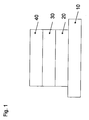
- FIG. 12 shows a schematic side view of an electronic device comprising a substrate 10, a first electrode 20, an emission layer 30 and a second electrode 40.
- the first electrode may be an anode and the second electrode may be a cathode.
- the electronic device may be a bottom-emitting device or a top-emitting device, for example an OLED.
- the emission layer 30 may comprise a first, a second and a third matrix material and be doped with an emitter material.
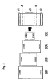
- FIG. 2 shows the schematic representation of the energy levels of the respective materials in the emission layer in one exemplary embodiment.
- the HOMO and LUMO of the first matrix material 30N, the second matrix material 30B and the third matrix material 30A are shown.
- the first matrix material has a HOMO which is lower in energy than the HOMO of the second matrix material and the third matrix material.
- the first matrix material has a LUMO which is higher in energy than the LUMO of the second matrix material and of the third matrix material.
- the second matrix material has a LUMO which is higher in energy than the LUMO of the third matrix material and a HOMO which is higher in energy than the HOMO of the third matrix material.
- the first matrix material has lower charge carrier mobilities than the two other matrix materials
- the second matrix material may comprise a hole transport material and the third matrix material may comprise an electron transport material.
- the emitter material 30E has a HOMO and LUMO which has the lowest bandgap compared to the matrix materials and lies between the LUMOs and the HOMOs of the three matrix materials.
- the layer may also be a charge carrier transport, charge carrier injection, or charge carrier blocking layer. You can also continue several emitter materials are used.
- the emitter material has a concentration of ⁇ 10% by weight in the emission layer.
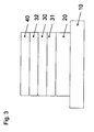
- FIG. 3 shows the schematic side view of another embodiment of the electronic device having an emission layer 30 to each of which on one side an electron transport layer 32 and a hole transport layer 31 adjacent.
- the first electrode 20 is an anode.
- Both the emission layer 30 and the electron transport layer 32 and the hole transport layer 31 may have matrices composed of three or more matrix materials.
- FIG. 4 shows the simulation of the charge carrier transport in an OLED in which an emission layer, a hole transport layer 31 and an electron transport layer 32 is present.
- the x-axis shows the distance of the respective layer from the anode D [nm]
- the y-axis shows the normalized recombination rate R n .
- FIG. 5 shows the schematic side view of a structure for the production of the electronic device.
- four evaporation sources 50 are applied to a holder 51, from which matrix materials and / or dopants can be vapor-deposited onto the deposition substrate 60.
- the evaporation rate is measured and adjusted via layer thickness monitors 55.
- the layer thickness monitors may, for example, be quartz crystals.
- the second matrix material, the hole transport material may be TCTA (9H-carbazole, 9,9 ', 9 "- (1,3,5-benzenetriyl) tris (9Cl)) and applied at a vapor deposition rate of 8 ⁇ / s
- the third electron-transport material may be, for example, TPBi (1,3,5-tris (N-phenylbenzylimidazol-2-yl) and applied at a vapor deposition rate of 8 ⁇ / s.)
- the emitter material may be the yellow emitter rubrene (5, 6,11,12-Tetraphenylnaphthacen) are introduced and with a vapor deposition rate of 0.2 ⁇ / s are applied, resulting in a layer with a volume concentration of 40% for the charge carrier transport materials and 1% for the emitter.
- Table 1 shows the HOMOs and LUMOs of these materials.
- the values of the HOMOs of TCTA, TPBi, mCP were determined by UV photoemission spectroscopy, the corresponding LUMO values were estimated by adding the energy required for the absorption to the HOMO value.
- the HOMO and LUMO values of rubrene were determined by cyclic voltammetry and photoelectron spectrometry.
- Table 1 HOMO [eV] LUMO [eV] mCP -5.9 -2.4 TCTA -5.7 -2.3 TPBi -6.3 -2.8 Rubren -5.5 -3.0
- the third matrix material TPBi has the lowest value for the LUMO in comparison with the other matrix materials and is thus an electron-transport material.
- the second matrix material TCTA has the largest value for the HOMO in comparison with the other matrix materials and is thus hole transport material.
- the first matrix material mCP is not involved in charge carrier transport as its LUMO is not lower than the LUMO of the third matrix material and its HOMO is not higher than the HOMO of the second matrix material.
- hole transport materials are: NPB N, N'-Bis (naphthalene-1-yl) -N, N'-bis (phenyl) benzidine TCTA 4,4 ', 4''- Tris (carbazol-9-yl) triphenylamine CPB 4,4'-bis biphenyl (carbazol-9-yl) 1T-NATA 4,4 ', 4 "-tris (N- (1-naphthyl) -N-phenyl-amino) triphenylamine Spiro-TAD 2,2 ', 7,7'-tetrakis (N, N-diphenylamino) -9,9'-spirobifluorene
- the first matrix material that has the lowest charge carrier mobility compared to the other matrix materials can be used: UGH-2 1,4-bis (triphenylsilyl) benzene UGH-3 1,3-bis (triphenylsilyl) benzene mCP 1,3-bis (carbazol-9-yl) benzene
- the HOMOs of UGH-2 and UGH-3 have values of -7.2 ⁇ 0.1 eV, the LUMOs are at 2.8 eV. These HOMO values can be determined by means of photoelectron spectroscopy, the LUMO values can be estimated from the distance of HOMO values and LUMO values at the intersection of the absorption and the fluorescence spectrum.
- Possible emitter materials are: Ir (ppy) 3 Tris (2-phenylpyridine) iridium (III) Ir (ppy) 2 Bis (2-phenylpyridlin) (acetylacetonate) iridium (II) (Acac) BCzVBi 4,4'-bis (9-ethyl-3-carbazovinylen) -1,1'-biphenyl FIrpic Bis (3,5-difluoro-2- (2-pyridyl) phenyl- (2-carboxy-pyridyl) iridium (III) Rubren tetraphenylnaphthacene Ir (piq) 3 Tris (1-phenylisoquinoline) iridium (III)
- emitter materials are small, non-polymeric molecules.
- polymeric emitter materials is also possible.
- Some of the electron and hole transport materials may also serve as the first matrix material.
- Important in composing the first, second and third matrix materials for the matrix are the relative ratios of the LUMOs and HOMOs of the three combined materials and their location to each other.
- the matrix can not be chosen arbitrarily for phosphorescent emitters due to the chemical compatibility.
- the red emitter iridium (III) bis (2-methyldibenzo [f, h] quinoxaline) acetylacetonate) is efficient only in an NBP matrix.
- NPB is a hole transport material. If there is still another emitter layer on the anode side, it will not be sufficiently supplied with electrons. By doping an electron transport material, such as BCP, the relative transport properties can be adjusted. The fine tuning of the transport properties is done with UGH4.
Description
Die Erfindung betrifft eine Elektronische Vorrichtung und ein Verfahren zur Herstellung einer elektronischen Vorrichtung.The invention relates to an electronic device and a method for producing an electronic device.
Diese Patentanmeldung beansprucht die Prioritäten der deutschen Patentanmeldung
Elektronische Vorrichtungen, wie beispielsweise organische Leuchtdioden (OLEDs), bestehen aus einer Abfolge mehrerer funktioneller organischer Schichten. Emissionsschichten weisen dabei ein Matrixmaterial auf, welches mit Emittermolekülen dotiert wird. In der Emissionsschicht werden Exzitonen durch Rekombination von Elektronen und "Löchern" gebildet, die zur Lichtemission führen. Um eine hohe Effizienz der elektronischen Vorrichtung zu erhalten, ist das Verhältnis zwischen Elektronen und "Löchern", die in der Emissionsschicht transportiert werden, entscheidend. Ein nicht ausgeglichenes Verhältnis zwischen Loch- und Elektronentransport resultiert in einer geringen Strahlungseffizienz der Vorrichtung.Electronic devices, such as organic light emitting diodes (OLEDs), consist of a sequence of multiple functional organic layers. Emission layers in this case have a matrix material which is doped with emitter molecules. In the emission layer, excitons are formed by recombination of electrons and "holes" that lead to light emission. In order to obtain high efficiency of the electronic device, the ratio between electrons and "holes" transported in the emission layer is crucial. An unbalanced relationship between hole and electron transport results in low radiation efficiency of the device.
Die Druckschrift
Aufgabe der Erfindung ist es, eine elektronische Vorrichtung bereitzustellen, die einen verbesserten Ladungsträgertransport und eine verbesserte Ladungsträgerbalance in den organischen Schichten und damit eine erhöhte Effizienz aufweist. Eine weitere Aufgabe der Erfindung ist es, ein Verfahren zur Herstellung einer elektronischen Vorrichtung bereitzustellen. Diese Aufgaben werden durch ein elektronische Vorrichtung gemäß Anspruch 1 und einem Verfahren zur Herstellung der elektronischen Vorrichtung gemäß Anspruch 12 gelöst. Weitere Ausführungsformen der Vorrichtung und des Verfahrens sind Gegenstand weiterer Ansprüche.The object of the invention is to provide an electronic device which has an improved charge carrier transport and an improved charge carrier balance in the organic layers and thus an increased Efficiency. Another object of the invention is to provide a method of manufacturing an electronic device. These tasks are through An electronic device according to claim 1 and a method for manufacturing the electronic device according to
Gemäß einer Ausführungsform wird eine elektronische Vorrichtung bereitgestellt, die ein Substrat, eine erste Elektrode, zumindest eine organische, funktionelle Schicht und eine zweite Elektrode umfasst, wobei die zumindest eine organische funktionelle Schicht zwischen der ersten Elektrode und der zweiten Elektrode angeordnet ist. Beispielsweise kann die erste Elektrode auf dem Substrat, die zumindest eine organische funktionelle Schicht auf der ersten Elektrode und die zweite Elektrode auf der zumindest einen organischen, funktionellen Schicht angeordnet sein. Die zumindest eine organische, funktionelle Schicht weist mindestens ein erstes Matrixmaterial, ein zweites Matrixmaterial und ein drittes Matrixmaterial auf, wobei das dritte Matrixmaterial ein Lowest Unoccupied Molecular Orbital (LUMO), das energetisch niedriger als das LUMO des zweiten Matrixmaterials und das LUMO des ersten Matrixmaterials ist, und wobei das zweite Matrixmaterial ein Highest Occupied Molecular Orbital (HOMO), das energetisch höher als das HOMO des ersten Matrixmaterials und das HOMO des dritten Matrixmaterials ist. Die zumindest eine organische, funktionelle Schicht ist eine Emissionsschicht und mit zumindest einem Emittermaterial dotiert.According to one embodiment, an electronic device is provided which comprises a substrate, a first electrode, at least one organic, functional layer and a second electrode, wherein the at least one organic functional layer is arranged between the first electrode and the second electrode. By way of example, the first electrode may be arranged on the substrate, the at least one organic functional layer on the first electrode, and the second electrode on the at least one organic, functional layer. The at least one organic functional layer comprises at least a first matrix material, a second matrix material and a third matrix material, wherein the third matrix material is a Lowest Unoccupied Molecular Orbital (LUMO) which is lower in energy than the LUMO of the second matrix material and the LUMO of the first matrix material and wherein the second matrix material is a Highest Occupied Molecular Orbital (HOMO) that is higher in energy than the HOMO of the first matrix material and the HOMO of the third matrix material. The at least one organic, functional layer is an emission layer and doped with at least one emitter material.
Damit wird eine elektronische Vorrichtung bereitgestellt, die mehr als zwei verschiedene Matrixmaterialien in einer organischen funktionellen Schicht umfasst. Dabei können drei verschiedene Matrixmaterialien vorhanden sein, je nach Bedarf auch mehr als drei.This provides an electronic device comprising more than two different matrix materials in an organic functional layer. There may be three different matrix materials, and more than three as needed.
Nach der Molekülorbitaltheorie sind in einem Molekül verschiedene Molekülorbitale mit verschiedenen Energieniveau vorhanden, die von den vorhandenen Elektronen besetzt werden können. Diese Molekülorbitale werden nach zunehmendem Energieniveau besetzt. Das LUMO ist das energetisch niedrigste Molekülorbital, das nicht mehr mit einem Elektron besetzt ist. Das HOMO ist das energetisch am höchsten gelegene Molekülorbital, das noch mit einem Elektron besetzt ist.According to the molecular orbital theory, in a molecule are different molecular orbitals with different energy levels present, which can be occupied by the existing electrons. These molecular orbitals are occupied according to increasing energy levels. The LUMO is the lowest energy molecular orbital that is no longer occupied by an electron. The HOMO is the highest molecular orbital in terms of energy, which is still occupied by an electron.
Diese elektronische Vorrichtung weist einen verbesserten Ladungsträgertransport und eine verbesserte Ladungsträgerbalance in der organischen funktionellen Schicht auf, und ein anpassbares Verhältnis zwischen Loch- und Elektronentransport. Das erste Matrixmaterial ist dabei so gewählt, dass es eine große Bandlücke, also die Differenz zwischen HOMO und LUMO aufweist, beispielsweise so dass sein HOMO energetisch unter dem HOMO der anderen beiden Matrixmaterialien und sein LUMO energetisch über dem LUMO der anderen beiden Matrixmaterialien liegt.This electronic device has improved charge carrier transport and carrier balance in the organic functional layer, and an adaptable hole-to-electron transport relationship. The first matrix material is chosen such that it has a large band gap, ie the difference between HOMO and LUMO, for example so that its HOMO lies energetically below the HOMO of the other two matrix materials and its LUMO energetically above the LUMO of the other two matrix materials.
Weiterhin kann das erste Matrixmaterial ein LUMO aufweisen, das energetisch höher als das LUMO des zweiten Matrixmaterials und das LUMO des dritten Matrixmaterials ist, und ein HOMO, das energetisch niedriger als das HOMO des zweiten Matrixmaterials und das HOMO des dritten Matrixmaterials ist.Furthermore, the first matrix material may have a LUMO that is higher in energy than the LUMO of the second matrix material and the LUMO of the third matrix material, and a HOMO that is lower in energy than the HOMO of the second matrix material and the HOMO of the third matrix material.
Weiterhin kann in der elektronischen Vorrichtung das zweite Matrixmaterial ein LUMO, das energetisch höher als das LUMO des dritten Matrixmaterials ist, und ein HOMO, das energetisch höher als das HOMO des dritten Matrixmaterials ist, aufweisen. Damit kann das erste Matrixmaterial die größte Bandlücke zwischen HOMO und LUMO im Vergleich zum zweiten und zum dritten Matrixmaterial aufweisen und das zweite Matrixmaterial weist eine Bandlücke auf, die zu der Bandlücke des dritten Matrixmaterials energetisch verschoben ist. Damit können auf dem LUMO des dritten Matrixmaterials Elektronen transportiert werden, und auf dem HOMO des zweiten Matrixmaterials Löcher transportiert werden, da diese Energieniveaus jeweils am energetisch günstigsten für den jeweiligen Ladungstransport sind.Furthermore, in the electronic device, the second matrix material may have a LUMO higher in energy than the LUMO of the third matrix material and a HOMO higher in energy than the HOMO of the third matrix material. Thus, the first matrix material may have the largest band gap between HOMO and LUMO compared to the second and the third matrix material and the second matrix material has a bandgap which is energetically shifted to the bandgap of the third matrix material. Thus, electrons can be transported on the LUMO of the third matrix material, and holes can be transported on the HOMO of the second matrix material, since these energy levels are the most energetically favorable for the respective charge transport.
Das erste Matrixmaterial kann in der elektronischen Vorrichtung eine Ladungsträgermobilität aufweisen, die geringer ist als die Ladungsträgermobilität des zweiten und des dritten Matrixmaterials. Das erste Matrixmaterial kann ein Ultra Wide Band Gap (UGH)-Material sein, welches eine im Vergleich zu den übrigen Matrixmaterialien große Bandlücke aufweist. Dadurch kann es keinen Anteil am Ladungsträgertransport aufweisen.The first matrix material may have in the electronic device a charge carrier mobility that is less than the charge carrier mobility of the second and the third matrix material. The first matrix material may be an Ultra Wide Band Gap (UGH) material which has a large band gap compared to the other matrix materials. As a result, it can not have any share in the transport of charge carriers.
Das zweite Matrixmaterial kann weiterhin ein Lochtransportmaterial umfassen und das dritte Matrixmaterial kann ein Elektronentransportmaterial umfassen.The second matrix material may further comprise a hole transport material and the third matrix material may comprise an electron transport material.
Der Ladungsträgertransport, also der Lochtransport und der Elektronentransport, hängt insbesondere von der Mobilität der Löcher beziehungsweise der Elektronen in einem Material und von der Lage der Energieniveaus HOMO und LUMO der Matrixmaterialien ab. Das HOMO und LUMO eines Materials ist dabei für die Ladungsträgerinjektion verantwortlich.The charge carrier transport, ie the hole transport and the electron transport, depends in particular on the mobility of the holes or the electrons in a material and on the location of the energy levels HOMO and LUMO of the matrix materials. The HOMO and LUMO of a material is responsible for the charge carrier injection.
Zur Erzeugung eines Lochs in der Matrix, die sich aus den drei Matrixmaterialien zusammensetzt, muss beispielsweise ein Elektron aus dem HOMO entfernt werden, was bei einem energetisch tief liegenden HOMO schwieriger ist als bei einem energetisch höher liegenden. Somit ist das zweite Matrixmaterial, das ein höher gelegenes HOMO als das dritte Matrixmaterial aufweist, besser als Lochtransportmaterial geeignet, als das dritte Matrixmaterial. Analoges gilt für die Erzeugung von Elektronen in LUMOs, die bei energetisch tiefer gelegenen LUMOs energetisch begünstigt ist. Somit eignet sich das dritte Matrixmaterial, das ein niedrigeres LUMO als das zweite Matrixmaterial aufweist, als Elektronentransportmaterial.To create a hole in the matrix, which is composed of the three matrix materials, for example, an electron must be removed from the HOMO, which is more difficult in an energetically low lying HOMO than in an energetically higher lying. So that's the second one Matrix material having a HOMO higher than the third matrix material, better suited as a hole transport material than the third matrix material. The same applies to the generation of electrons in LUMOs, which is energetically favored at energetically lower LUMOs. Thus, the third matrix material having a lower LUMO than the second matrix material is suitable as an electron transport material.
Sind Löcher und Elektronen erzeugt, spielt weiterhin die Mobilität dieser Ladungsträger in dem Material eine Rolle. Je nachdem, wie diese beiden Faktoren in einem Material zusammenwirken, kann ein Matrixmaterial als Elektronentransportmaterial oder als Lochtransportmaterial dienen. Dabei findet jeweils auch der Ladungsträgertransport der anderen Ladung statt, es überwiegt jedoch der Transport eines Ladungsträgers. Findet in einem Matrixmaterial kein Ladungsträgertransport statt, wie in einer Ausführungsform der Erfindung in dem ersten Matrixmaterial, so kann das entweder darauf zurückzuführen sein, dass keine Ladungsträger erzeugt werden oder dass keine Mobilität der Ladungsträger vorhanden ist. Neben dem ersten Matrixmaterial können weitere Matrixmaterialien in der organischen, funktionellen Schicht vorhanden sein, die nicht zum Ladungsträgertransport beitragen.If holes and electrons are generated, the mobility of these charge carriers in the material also plays a role. Depending on how these two factors interact in a material, a matrix material may serve as an electron transport material or as a hole transport material. In each case, the charge carrier transport of the other charge takes place, but it predominates the transport of a charge carrier. If no charge carrier transport takes place in a matrix material, as in one embodiment of the invention in the first matrix material, this can either be due to the fact that no charge carriers are generated or that there is no mobility of the charge carriers. In addition to the first matrix material, further matrix materials may be present in the organic, functional layer that do not contribute to the charge carrier transport.
Die Energieniveaus HOMO und LUMO eines Materials können gemessen werden, um geeignete Materialien für erstes, zweites und drittes Matrixmaterial auszuwählen. So kann das HOMO eines Materials mittels Cyclovoltametrie bestimmt werden. Die Bandlücke, also der energetische Unterschied zwischen HOMO und LUMO kann weiterhin mittels Spektroskopie ermittelt werden, bei der die Wellenlänge des emittierten Lichts gemessen wird und daraus die entstandenen Exzitonen und die Bandlücke berechnet wird. Das Energieniveau des LUMO wird dann aus dem ermittelten HOMO und der Bandlücke berechnet. Das HOMO kann alternativ auch mittels Photoelektronenspektroskopie ermittelt werden.The energy levels HOMO and LUMO of a material can be measured to select suitable materials for first, second and third matrix materials. Thus, the HOMO of a material can be determined by cyclic voltammetry. The band gap, ie the energetic difference between HOMO and LUMO, can still be determined by means of spectroscopy, in which the wavelength of the emitted light is measured and from this the resulting excitons and the band gap is calculated. The energy level of the LUMO is then calculated from the determined HOMO and the bandgap. The HOMO can alternatively be determined by means of photoelectron spectroscopy.
Die Mobilität von Elektronen und Löchern kann von dem Molekülabstand, also dem mittleren Abstand von Ladungsträgertransportierenden Molekülen in dem jeweiligen Matrixmaterial abhängen. Somit spielt die Konzentration eines Matrixmaterials in der Mischung mehrerer Matrixmaterialien eine Rolle. Das erste Matrixmaterial, das im Vergleich zu dem zweiten und dritten Matrixmaterial die größte Bandlücke und die geringste Ladungsträgermobilität aufweist, kann dazu dienen, die Konzentration des zweiten und des dritten Matrixmaterials getrennt voneinander einzustellen. Je nach der gewählten Konzentration des zweiten und dritten Matrixmaterials ändern sich die Abstände zwischen den jeweiligen Molekülen. Der mikroskopische Ladungsträgertransport hängt vom Molekülabstand der Ladungsträgertransportierenden Moleküle in dem jeweiligen Matrixmaterial ab, sodass sich durch die Einstellung der Konzentration die Mobilität von Elektronen und Löchern in der Matrix, die zumindest drei Matrixmaterialien aufweist, getrennt voneinander absolut einstellen lässt.The mobility of electrons and holes may depend on the molecular distance, ie the average distance of charge carrier transporting molecules in the respective matrix material. Thus, the concentration of a matrix material in the mixture of several matrix materials plays a role. The first matrix material, which has the largest band gap and the lowest charge carrier mobility compared to the second and third matrix material, can serve to set the concentration of the second and the third matrix material separately from one another. Depending on the selected concentration of the second and third matrix material, the distances between the respective molecules change. The microscopic charge carrier transport depends on the molecular distance of the charge carrier-transporting molecules in the respective matrix material, so that the adjustment of the concentration allows the mobility of electrons and holes in the matrix, which has at least three matrix materials, to be set absolutely separately.
Nach Miller und Abraham kann die Mobilität folgendermaßen bestimmt werden: ![]()
![]()
In diesem Modell wird ein Festkörper schematisch gesehen aus den Plätzen i und j aufgebaut, auf denen sich die Ladungsträger befinden können. Jeder Platz repräsentiert einen lokalisierten Zustand. Der Transport eines Ladungsträgers zwischen den Plätzen i und j wird durch einen Widerstand Rij dargestellt. Die Größe des temperaturabhängigen Widerstands spiegelt dabei den räumlichen Abstand zwischen den Plätzen und die benötigte Aktivierungsenergie für den Übergang wider. Der Parameter y steht für den Abfall der elektronischen Wellenfunktion der Ladungsträger, a ist der Parameter für den durchschnittlichen Gitterabstand. Die Phononenfrequenz v0 gibt die Anzahl der Versuche eines Ladungsträgers aus einem lokalisierten Zustand in einen anderen lokalisierten Zustand zu gelangen an, liegt im Bereich von etwa 1013 s-1 und berücksichtigt die Stärke der Elektronenphononkopplung.In this model, a solid body is schematically constructed from the places i and j, on which the Charge carriers can be located. Each place represents a localized state. The transport of a charge carrier between the locations i and j is represented by a resistor Rij. The magnitude of the temperature-dependent resistance reflects the spatial distance between the sites and the required activation energy for the transition. The parameter y stands for the fall of the electronic wave function of the charge carriers, a is the parameter for the average grid spacing. The phonon frequency v 0 indicates the number of attempts of a charge carrier from a localized state to reach a different localized state, is in the range of about 10 13 s -1 and takes into account the strength of electron phonon coupling.
Die elektronische Vorrichtung kann weiterhin eine organische, funktionelle Schicht aufweisen, die aus einer Gruppe ausgewählt ist, die Emissionsschichten, Elektronentransportschichten, Lochtransportschichten, Elektronenblockierschichten, Lochblockierschichten, Lochinjektionsschichten, Elektroneninjektionsschichten und Zwischenschichten umfasst. Mit Zwischenschichten werden Schichten bezeichnet, die zwischen zwei Emissionsschichten angeordnet sind. Je nachdem, was für eine organische, funktionelle Schicht ausgewählt wird, können diese Schichten noch zusätzliche Dotierstoffe enthalten. Die organische, funktionelle Schicht kann eine Emissionsschicht sein und mit zumindest einem Emittermaterial dotiert sein. Emittermaterialien können kleine Moleküle oder Polymere umfassen. Die Konzentration des Emittermaterials in einer Emissionsschicht kann bis zu 10 Gew% betragen. Weiterhin kann das Emittermaterial aufgrund der niedrigen Konzentration in der Emissionsschicht nur eine geringe Ladungsträgermobilität aufweisen und damit nur geringfügig zum Ladungsträgertransport beitragen.The electronic device may further comprise an organic functional layer selected from the group consisting of emission layers, electron transport layers, hole transport layers, electron blocking layers, hole blocking layers, hole injection layers, electron injection layers, and intermediate layers. Intermediate layers refer to layers which are arranged between two emission layers. Depending on what is selected for an organic, functional layer, these layers may contain additional dopants. The organic, functional layer may be an emission layer and doped with at least one emitter material. Emitter materials can include small molecules or polymers. The concentration of the emitter material in an emission layer can be up to 10% by weight. Furthermore, due to the low concentration in the emission layer, the emitter material can only have a low charge carrier mobility and thus contribute only slightly to the charge carrier transport.
In der Emissionsschicht können auch zwei oder drei Emittermaterialien vorhanden sein. Die Emittermaterialien können beispielsweise ausgewählt sein aus dem grün emittierenden Ir(ppy)3 (Tris(2-phenylpyridin)iridium(III)), dem rot emittierenden Ir(piq)3 (Tris(1-phenylisoquinolin)iridium(III)) oder dem blau emittierenden Firpic (Bis(3,5-Difluoro-2-(2-pyridyl)phenyl-(2-carboxypyridyl)iridium(III)).Two or three emitter materials may also be present in the emission layer. The emitter materials may be selected, for example, from the green emitting Ir (ppy) 3 (tris (2-phenylpyridine) iridium (III)), the red emitting Ir (piq) 3 (tris (1-phenylisoquinoline) iridium (III)) or the blue-emitting Firpic (bis (3,5-difluoro-2- (2-pyridyl) phenyl- (2-carboxypyridyl) iridium (III)).
Die Konzentrationen des Emittiermaterials und der Matrixmaterialien in der organischen funktionellen Schicht können innerhalb der organischen funktionellen Schicht einen Gradienten aufweisen. Damit kann beispielsweise die Konzentration des Emittermaterials in einem ersten Teilbereich der Schicht höher sein als in einem zweiten Teilbereich der Schicht.The concentrations of the emissive material and the matrix materials in the organic functional layer may have a gradient within the organic functional layer. Thus, for example, the concentration of the emitter material in a first portion of the layer may be higher than in a second portion of the layer.
Durch Verzicht auf die Dotierung mit Emittermaterialien lassen sich Transport-, Zwischen- und Blockierschichten herstellen.By dispensing with the doping with emitter materials, transport, intermediate and blocking layers can be produced.
In einer elektronischen Vorrichtung können auch mehrere organische, funktionelle Schichten vorhanden sein, wobei die Schichten unterschiedliche Funktionen oder gleiche Funktionen aufweisen können. Beispielsweise kann eine elektronische Vorrichtung eine Abfolge mehrerer funktioneller, organischer Schichten aufweisen, die beispielsweise zusammengesetzt ist aus einer Lochinjektionsschicht, einer Lochtransportschicht, einer ersten Emissionsschicht, einer Zwischenschicht, einer zweiten Emissionsschicht, einer Elektronentransportschicht und einer Elektroneninjektionsschicht. Jede dieser Schichten kann eine Matrix aufweisen, die mindestens ein erstes, ein zweites und ein drittes Matrixmaterial aufweist. Die Matrixmaterialien in den verschiedenen organischen funktionellen Schichten können in allen Schichten gleich oder unterschiedlich gewählt werden.In an electronic device also several organic functional layers may be present, wherein the layers may have different functions or the same functions. For example, an electronic device may comprise a sequence of a plurality of functional, organic layers, which is composed, for example, of a hole injection layer, a hole transport layer, a first emission layer, an intermediate layer, a second emission layer, an electron transport layer and an electron injection layer. Each of these layers may comprise a matrix having at least a first, a second and a third matrix material. The matrix materials in the various organic functional layers can be chosen the same or different in all layers.
Je nachdem, wo sich die Emissionsschicht in dem Schichtstapel der elektronischen Vorrichtung befindet, kann dort die Mobilität von Elektronen und Löchern innerhalb dieser Schicht getrennt voneinander optimiert werden, wenn die Emissionsschicht ein erstes, ein zweites und ein drittes Matrixmaterial aufweist. Die Mobilität kann auch über mehrere Schichten hinweg optimiert werden.Depending on where the emission layer is located in the layer stack of the electronic device, the mobility of electrons and holes within that layer can be optimized separately therefrom, if the emission layer has a first, a second and a third matrix material. Mobility can also be optimized over several shifts.
Auch wenn die Emissionsschicht, die die drei Matrixmaterialien aufweist, nahe einer Anode oder einer Kathode liegt, kann die Mobilität von Elektronen und Löchern so eingestellt werden, dass das Verhältnis von Löchern und Elektronen in der Emissionsschicht ausgeglichen ist. Je nachdem, welche Ladungsträgersorte eine höhere Beweglichkeit aufweisen soll, kann die Matrix eine höhere Konzentration des jeweiligen Matrixmaterials enthalten. So kann in der Emissionsschicht, unabhängig von der Lage der Emissionsschicht der elektronischen Vorrichtung, eine hohe Anzahl an Exzitonen gebildet werden.Although the emission layer comprising the three matrix materials is near an anode or a cathode, the mobility of electrons and holes can be adjusted to balance the ratio of holes and electrons in the emission layer. Depending on which charge carrier type is to have a higher mobility, the matrix may contain a higher concentration of the respective matrix material. Thus, in the emission layer, regardless of the position of the emission layer of the electronic device, a large number of excitons are formed.
Wenn die organische, funktionelle Schicht eine Emissionsschicht mit einem Emittermaterial ist, kann das LUMO des Emittermaterials energetisch niedriger als das LUMO des ersten, zweiten und dritten Matrixmaterials sein und das HOMO des Emittermaterials energetisch höher als das HOMO des ersten, zweiten und dritten Matrixmaterials sein. Somit ist die Bandlücke zwischen HOMO und LUMO des Emittermaterials kleiner als die Bandlücken der drei Matrixmaterialien und liegt zudem energetisch zwischen allen Bandlücken aller Matrixmaterialien. Ein ambipolarer Ladungstransport in einer Emissionsschicht ist somit möglich.When the organic functional layer is an emitter material emitting layer, the emitter material LUMO may be lower in energy than the LUMO of the first, second and third matrix materials and the HOMO of the emitter material may be higher in energy than the HOMO of the first, second and third matrix materials. Thus is the bandgap between HOMO and LUMO of the emitter material is smaller than the bandgaps of the three matrix materials and lies energetically between all band gaps of all matrix materials. An ambipolar charge transport in an emission layer is thus possible.
Die Moleküle des zweiten und dritten Matrixmaterials transportieren bevorzugt nur jeweils eine Ladungsträgersorte, Löcher oder Elektronen, somit bilden sich auf ihnen keine Exzitonen. Damit wird die Lebensdauer der Materialien erhöht, da keine Degradation durch Anregungsenergie stattfinden kann. Zwischen den verschiedenen Molekülen der Matrixmaterialien entstehen angeregte Zustände (Eximere), die ihre Anregungsenergie durch Energietransfer auf die Emittermoleküle übertragen können. Somit wird die Effizienz der elektronischen Vorrichtung weiterhin erhöht.The molecules of the second and third matrix materials preferably transport only one charge carrier type each, holes or electrons, so that no excitons are formed on them. Thus, the life of the materials is increased, since no degradation can take place by excitation energy. Excited states (eximers), which can transfer their excitation energy to the emitter molecules through energy transfer, arise between the different molecules of the matrix materials. Thus, the efficiency of the electronic device is further increased.
Eine elektronische Vorrichtung kann auch mehrere Emissionsschichten aufweisen, beispielsweise um phosphoreszente und fluoreszente Emittermaterialien in einer Vorrichtung zu kombinieren. Dann kann das Einfügen einer Zwischenschicht zwischen den Emissionsschichten notwendig sein, die beispielsweise ambipolare Ladungstransporteigenschaften aufweisen kann. Dies ist durch die Kombination von drei Matrixmaterialien möglich.An electronic device may also have multiple emission layers, for example to combine phosphorescent and fluorescent emitter materials in one device. Then it may be necessary to insert an intermediate layer between the emission layers which may, for example, have ambipolar charge transport properties. This is possible by combining three matrix materials.
Durch Einstellung der Ladungsträgermobilität mit Hilfe der drei Matrixmaterialien ist es möglich, die Lage der Rekombinationszone in einer Emissionsschicht gezielt zu beeinflussen. Die Rekombinationszone kann sich dabei innerhalb einer Schicht oder über mehrere Schichten verteilt befinden. Durch die Einführung der ersten Matrix, die keinen Ladungstransport aufweist, innerhalb einer Emissionsschicht sinkt der absolute Wert der Ladungsträgermobilität. Daraus ergibt sich eine Rekombinationszone, die Zone in der Exzitonen gebildet werden, die von den Rändern einer emittierenden Schicht zur Mitte hin verschoben wird. Dies erhöht die Effizienz der Vorrichtung, da unter anderem die nicht strahlende Abregung von Exzitonen (Quenching) vermindert wird und mehr Exzitonen in der eigentlichen Emissionsschicht gebildet werden, statt in den angrenzenden Schichten.By adjusting the charge carrier mobility with the aid of the three matrix materials, it is possible to specifically influence the position of the recombination zone in an emission layer. The recombination zone may be distributed within a layer or over several layers. By introducing the first matrix, which has no charge transport, within an emission layer the absolute value of the charge carrier mobility decreases. This results in a recombination zone, the zone formed in the exciton, which is shifted from the edges of an emitting layer towards the center. This increases the efficiency of the device, since inter alia the non-radiative excitation of excitons (quenching) is reduced and more excitons are formed in the actual emission layer, rather than in the adjacent layers.
Bei der elektronischen Vorrichtung kann es sich um eine strahlungsemittierende Vorrichtung beispielsweise um eine organische Licht emittierende Vorrichtung handeln. Diese Licht emittierende Vorrichtung kann eine organische, Licht emittierende Diode (OLED) sein.The electronic device may be a radiation-emitting device, for example an organic light-emitting device. This light emitting device may be an organic light emitting diode (OLED).
Beispielsweise ist eine organische, funktionelle Schicht bei einem Transistor zwischen einer ersten und zweiten Elektrode angeordnet. Weiterhin ist eine dritte Elektrode vorhanden. Die Elektroden können aus Gate-, Source- und Drain-Elektrode ausgewählt sein. Ein Transistor kann zum Schalten oder Verstärken von elektrischen Signalen verwendet werden.For example, an organic functional layer is disposed in a transistor between a first and second electrode. Furthermore, a third electrode is present. The electrodes may be selected from gate, source and drain electrodes. A transistor can be used to switch or amplify electrical signals.
Bei einer Solarzelle kann Licht in elektrische Energie umgewandelt werden. Hier ist eine organische, funktionelle Schicht zwischen einer ersten und einer zweiten Elektrode angeordnet, wobei zumindest eine der Elektroden transparent ausgeformt ist.In a solar cell, light can be converted into electrical energy. Here, an organic, functional layer is arranged between a first and a second electrode, wherein at least one of the electrodes is formed in a transparent manner.
Die Vorrichtung kann in einer organischen funktionellen Schicht als erstes Matrixmaterial beispielsweise mCP (m-Bis(N-carbazolylbenzol)), als zweites Matrixmaterial, das ein Lochtransportmaterial sein kann, TCTA (9H-carbazol,9,9',9"-(1,3,5-Benzoltriyl)tris-(9Cl)), und als drittes Matrixmaterial, das ein Elektronentransportmaterial sein kann, beispielsweise TPBi (1,3,5-Tris(N-Phenylbenzylimidazol-2-yl) aufweisen. Soll eine Matrix für eine Emissionsschicht bereitgestellt werden, kann als Emittermaterial beispielsweise der gelbe Emitter Rubren (5,6,11,12-Tetraphenylnaphthacen) eingefügt werden.The device may be in an organic functional layer as the first matrix material, for example mCP (m-bis (N-carbazolylbenzene)), as a second matrix material, which may be a hole transport material, TCTA (9H-carbazole, 9,9 ', 9 "- (1 , 3,5-benzenetriyl) tris (9Cl)), and as the third matrix material, which may be an electron transport material, for example TPBi (1,3,5-tris (N-phenylbenzylimidazol-2-yl)) An emission layer may be provided, for example the yellow emitter rubrene (5,6,11,12-tetraphenylnaphthacene) may be incorporated as emitter material.
Es wird weiterhin ein Verfahren zur Herstellung einer elektronischen Vorrichtung mit den oben beschriebenen Eigenschaften bereitgestellt. Das Verfahren umfasst die Verfahrensschritte A) Bereitstellen eines Substrats, B) Bereitstellen einer ersten Elektrode und einer zweiten Elektrode, C) Anordnen zumindest einer organischen Schicht zwischen der ersten Elektrode und der zweiten Elektrode Beispielsweise kann die zumindest eine organische, funktionelle Schicht auf der ersten Elektrode und die zweite Elektrode auf der organischen, funktionellen Schicht angeordnet werden. Im Verfahrensschritt C) wird dabei mindestens ein erstes Matrixmaterial, ein zweites Matrixmaterial und ein drittes Matrixmaterial gleichzeitig aufgebracht. Das Aufbringen im Verfahrensschritt C) kann beispielsweise durch Aufdampfen (Koevaporation) geschehen. Durch das gleichzeitige Aufbringen kann die Konzentration des jeweiligen Matrixmaterials unabhängig von den anderen Matrixmaterialien bestimmt werden, sodass die Matrixmaterialien in verschiedenen Konzentrationen aufgebracht werden können.There is further provided a method of manufacturing an electronic device having the characteristics described above. The method comprises the method steps A) providing a substrate, B) providing a first electrode and a second electrode, C) arranging at least one organic layer between the first electrode and the second electrode. For example, the at least one organic, functional layer on the first electrode and the second electrode are disposed on the organic functional layer. In method step C), at least one first matrix material, a second matrix material and a third matrix material are applied simultaneously. The application in process step C) can be done, for example, by vapor deposition (coevaporation). By simultaneous application, the concentration of the respective matrix material can be determined independently of the other matrix materials, so that the matrix materials can be applied in different concentrations.
Anhand der Figuren und Ausführungsbeispiele soll die Erfindung näher erläutert werden:
- Figur 1
- zeigt die schematische Seitenansicht einer elektronischen Vorrichtung,
- Figur 2
- zeigt eine schematische Ansicht der energetischen Zustände der verschiedenen Matrixmaterialien,
- Figur 3
- zeigt eine schematische Seitenansicht einer elektronischen Vorrichtung,
- Figur 4
- zeigt die Simulation der Mobilität der Ladungsträger in einer Emissionsschicht,
- Figur 5
- zeigt den schematischen Aufbau zur Herstellung einer Schicht mit mehreren Matrixmaterialien.
- FIG. 1
- shows the schematic side view of an electronic device,
- FIG. 2
- shows a schematic view of the energetic states of the various matrix materials,
- FIG. 3
- shows a schematic side view of an electronic device,
- FIG. 4
- shows the simulation of the mobility of the charge carriers in an emission layer,
- FIG. 5
- shows the schematic structure for producing a layer with a plurality of matrix materials.
Das Emittermaterial 30E weist ein HOMO und LUMO auf, das die geringste Bandlücke im Vergleich zu den Matrixmaterialien hat und zwischen den LUMOs und den HOMOs der drei Matrixmaterialien liegt.The
Rechts in dem Schema ist die Summe der verschiedenen Energieniveaus aufgezeigt. A symbolisiert das Energieniveau, bei dem der Elektronentransport stattfindet, B symbolisiert das Energieniveau, bei dem Lochtransport stattfindet. d1 und d2 stehen für die energetischen Abstände zwischen den LUMOs des ersten und zweiten Matrixmaterials (d1) und den HOMOs des ersten und dritten Matrixmaterials (d2). d3 symbolisiert die Bandlücke des Emittermaterials. Wird kein Emittermaterial eingesetzt, kann es sich bei der Schicht auch um eine Ladungsträgertransport-, Ladungsträgerinjektions- oder Ladungsträgerblockierschicht handeln. Weiterhin können auch mehrere Emittermaterialien eingesetzt werden. Das Emittermaterial weist in der Emissionsschicht eine Konzentration von ≤ 10 Gew% auf.On the right in the diagram the sum of the different energy levels is shown. A symbolizes the energy level at which the electron transport takes place, B symbolizes the energy level at which hole transport takes place. d1 and d2 represent the energetic distances between the LUMOs of the first and second matrix materials (d1) and the HOMOs of the first and third matrix materials (d2). d3 symbolizes the band gap of the emitter material. If no emitter material is used, the layer may also be a charge carrier transport, charge carrier injection, or charge carrier blocking layer. You can also continue several emitter materials are used. The emitter material has a concentration of ≦ 10% by weight in the emission layer.
Bei der Simulation wurden Elektronen- und Lochmobilität in der Emissionsschicht gleichgesetzt, also ein ambipolarer Ladungstransport angenommen. Es wurde ohmsche Injektion angenommen, alle Energiebarrieren zwischen HOMO und LUMO der zwei Schichten betrugen 400 meV für die jeweilige Ladungsträgersorte. In dem Diagramm sind für die verschiedenen Linienformen die jeweiligen Mobilitäten der Ladungsträger in m2/Vs angegeben, sie bewegen sich zwischen 10-8 bis zu 10-12.In the simulation, electron and hole mobility in the emission layer were equated, ie an ambipolar charge transport was assumed. It was ohmic injection Assuming all the energy barriers between HOMO and LUMO of the two layers were 400 meV for each type of charge carrier. In the diagram, the respective mobilities of the charge carriers in m 2 / Vs are indicated for the different line shapes, they range between 10 -8 to 10 -12 .
Beispielsweise kann mit einem Aufbau gemäß
Das dritte Matrixmaterial TPBi weist den im Vergleich mit den anderen Matrixmaterialien niedrigsten Wert für das LUMO auf und ist somit Elektronentransportmaterial. Das zweite Matrixmaterial TCTA weist den im Vergleich mit den anderen Matrixmaterialien größten Wert für das HOMO auf und ist somit Lochtransportmaterial. Das erste Matrixmaterial mCP ist nicht am Ladungsträgertransport beteiligt, da sein LUMO nicht niedriger als das LUMO des dritten Matrixmaterials ist und sein HOMO nicht höher als das HOMO des zweiten Matrixmaterials ist.The third matrix material TPBi has the lowest value for the LUMO in comparison with the other matrix materials and is thus an electron-transport material. The second matrix material TCTA has the largest value for the HOMO in comparison with the other matrix materials and is thus hole transport material. The first matrix material mCP is not involved in charge carrier transport as its LUMO is not lower than the LUMO of the third matrix material and its HOMO is not higher than the HOMO of the second matrix material.
Weitere mögliche Lochtransportmaterialien sind:
Als Elektronentransportmaterialien können weiterhin eingesetzt werden:
Als erstes Matrixmaterial, das im Vergleich zu den anderen Matrixmaterialien die geringste Ladungsträgermobilität aufweist, kann eingesetzt werden:
Die HOMOs von UGH-2 und UGH-3 haben Werte von -7,2 ± 0,1 eV, die LUMOs liegen bei 2,8 eV. Diese HOMO-Werte können mittels Photoelektronenspektroskopie bestimmt werden, die LUMO-Werte können aus dem Abstand von HOMO-Werten und LUMO-Werten am Schnittpunkt des Absorptions- und des Fluoreszenzspektrums abgeschätzt werden.The HOMOs of UGH-2 and UGH-3 have values of -7.2 ± 0.1 eV, the LUMOs are at 2.8 eV. These HOMO values can be determined by means of photoelectron spectroscopy, the LUMO values can be estimated from the distance of HOMO values and LUMO values at the intersection of the absorption and the fluorescence spectrum.
Mögliche Emittermaterialien sind:
Bei diesen Emittermaterialien handelt es sich um kleine, nicht-polymere Moleküle. Der Einsatz von polymeren Emittermaterialien ist ebenso möglich.These emitter materials are small, non-polymeric molecules. The use of polymeric emitter materials is also possible.
Weitere mögliche Materialien, die je nach Lage ihrer HOMOs und LUMOs zueinander als erste, zweite oder dritte Matrix eingesetzt werden können, sind:
Einige der Elektronen- und Lochtransportmaterialien können auch als erstes Matrixmaterial dienen. Wichtig bei der Zusammenstellung des ersten, zweiten und dritten Matrixmaterials für die Matrix sind das relative Verhältnis der LUMOs und HOMOs der drei kombinierten Materialien und deren Lage zueinander.Some of the electron and hole transport materials may also serve as the first matrix material. Important in composing the first, second and third matrix materials for the matrix are the relative ratios of the LUMOs and HOMOs of the three combined materials and their location to each other.
Die Matrix kann für phosphoreszente Emitter aufgrund der chemischen Verträglichkeit nicht beliebig gewählt werden. Der rote Emitter Iridium (III)bis(2-methyldibenzo-[f,h]quinoxalin)-acetylacetonat) ist nur in einer NBP-Matrix effizient. NPB ist jedoch ein Lochtransportmaterial. Befindet sich nun anodenseitig noch eine weitere Emitterschicht, wird diese nicht ausreichend mit Elektronen versorgt. Durch Eindotierung eines Elektronentransportmaterials, beispielsweise BCP, können die relativen Transporteigenschaften eingestellt werden. Die Feinabstimmung der Transporteigenschaften erfolgt mit UGH4.The matrix can not be chosen arbitrarily for phosphorescent emitters due to the chemical compatibility. The red emitter iridium (III) bis (2-methyldibenzo [f, h] quinoxaline) acetylacetonate) is efficient only in an NBP matrix. However, NPB is a hole transport material. If there is still another emitter layer on the anode side, it will not be sufficiently supplied with electrons. By doping an electron transport material, such as BCP, the relative transport properties can be adjusted. The fine tuning of the transport properties is done with UGH4.
Die in den Figuren und Ausführungsbeispielen gezeigten Ausführungsformen können beliebig variiert werden. Es ist weiterhin zu berücksichtigen, dass sich die Erfindung nicht auf die Beispiele beschränkt, sondern weitere, hier nicht aufgeführte Ausgestaltungen zulässt.The embodiments shown in the figures and embodiments can be varied as desired. It should also be noted that the invention is not limited to the examples, but allows other, not listed here embodiments.
Claims (14)
- Electronic device, comprising- a substrate (10),- a first electrode (20),- at least one organic functional layer, and- a second electrode (40), wherein the at least one organic functional layer is arranged between the first electrode (20) and the second electrode (40) and wherein the at least one organic functional layer comprises at least a first matrix material (30N), a second matrix material (30B) and a third matrix material (30A) and the third matrix material (30A) has a lowest unoccupied molecular orbital (LUMO), that is energetically lower than the LUMO of the second matrix material (30B) and the LUMO of the first matrix material (30N), and wherein the second matrix material (30B) has a highest occupied molecular orbital (HOMO), that is energetically higher than the HOMO of the first matrix material (30N) and the HOMO of the third matrix material (30A), characterized in that the at least one organic functional layer is an emission layer and is doped with at least one emitter material (30E).
- Electronic device according to the preceding claim, wherein the first matrix material (30N) has a LUMO that is energetically higher than the LUMO of the second matrix material (30B) and the LUMO of the third matrix material (30A), and has a HOMO that is energetically lower than the HOMO of the second matrix material (30B) and the HOMO of the third matrix material (30A).
- Electronic device according to the preceding claim, wherein the second matrix material (30B) has a LUMO that is energetically higher than the LUMO of the third matrix material (30A), and has a HOMO that is energetically higher than the HOMO of the third matrix material (30A).
- Electronic device according to any of the preceding claims, wherein the first matrix material (30N) has a charge carrier mobility that is lower than the charge carrier mobilities of the second and the third matrix material (30A).
- Electronic device according to any of the preceding claims, wherein the second matrix material (30B) comprises a hole transport material.
- Electronic device according to any of the preceding claims, wherein the third matrix material (30A) comprises an electron transport material.
- Electronic device according to any of the preceding claims, which comprises further organic functional layers selected from a group comprising emission layers, electron transport layers, hole transport layers, electron blocking layers, hole blocking layers, hole injection layers, electron injection layers and intermediate layers.
- Electronic device according to any of the preceding claims, wherein the emitter material (30E) in the emission layer has a concentration of ≤ 10% by weight.
- Electronic device according to the preceding claim, wherein the concentration of the emitter material (30E) in the emission layer has a gradient.
- Electronic device according to any of the preceding claims, wherein the LUMO of the emitter material (30E) is energetically lower than the LUMO of the first, the second and the third matrix material (30B, 30A) and the HOMO of the emitter material (30E) is energetically higher than the HOMO of the first, the second and the third matrix material (30N, 30B, 30A).
- Electronic device according to any of the preceding claims, which is embodied as a radiation-emitting device.
- Electronic device according to any of Claims 1 to 10, which is embodied as an organic light-emitting device.
- Method for producing an electronic device according to Claims 1 to 12, comprising the following method steps:A) providing a substrate (10),B) providing a first electrode (20) and a second electrode (40),C) arranging at least one organic functional layer between the first electrode (20) and the second electrode (40), wherein in method step C) at least the first matrix material (30N), the second matrix material (30B) and the third matrix material (30A) are applied simultaneously.
- Method according to the preceding claim, wherein in method step C) the first matrix material (30N), the second matrix material (30B) and the third matrix material (30A) are applied by vapour deposition.
Applications Claiming Priority (3)
| Application Number | Priority Date | Filing Date | Title |
|---|---|---|---|
| DE102008025920 | 2008-05-30 | ||
| DE102008039361A DE102008039361A1 (en) | 2008-05-30 | 2008-08-22 | Electronic device |
| PCT/DE2009/000701 WO2009143807A1 (en) | 2008-05-30 | 2009-05-18 | Electronic device |
Publications (2)
| Publication Number | Publication Date |
|---|---|
| EP2281318A1 EP2281318A1 (en) | 2011-02-09 |
| EP2281318B1 true EP2281318B1 (en) | 2013-07-10 |
Family
ID=41254075
Family Applications (1)
| Application Number | Title | Priority Date | Filing Date |
|---|---|---|---|
| EP09753523.1A Active EP2281318B1 (en) | 2008-05-30 | 2009-05-18 | Electronic device |
Country Status (8)
| Country | Link |
|---|---|
| US (1) | US8723164B2 (en) |
| EP (1) | EP2281318B1 (en) |
| JP (1) | JP5222397B2 (en) |
| KR (2) | KR101559607B1 (en) |
| CN (2) | CN103268920B (en) |
| DE (1) | DE102008039361A1 (en) |
| TW (1) | TW201004468A (en) |
| WO (1) | WO2009143807A1 (en) |
Families Citing this family (13)
| Publication number | Priority date | Publication date | Assignee | Title |
|---|---|---|---|---|
| DE102008039361A1 (en) * | 2008-05-30 | 2009-12-03 | Osram Opto Semiconductors Gmbh | Electronic device |
| US9142791B2 (en) * | 2011-05-27 | 2015-09-22 | Universal Display Corporation | OLED having multi-component emissive layer |
| CN103931009B (en) | 2011-11-11 | 2018-01-19 | 三菱化学株式会社 | Organic electroluminescent device and organic electroluminescence device |
| KR102347025B1 (en) * | 2012-03-14 | 2022-01-03 | 가부시키가이샤 한도오따이 에네루기 켄큐쇼 | Light-emitting element |
| TW201535818A (en) * | 2013-10-25 | 2015-09-16 | Univ Michigan | Exciton management in organic photovoltaic multi-donor energy cascades |
| US10674573B2 (en) * | 2014-12-02 | 2020-06-02 | Universiteit Gent | Light emission device with anisotropic properties |
| GB2538325A (en) * | 2015-05-15 | 2016-11-16 | Cambridge Display Tech Ltd | Organic light-emitting device |
| KR102500272B1 (en) | 2015-09-16 | 2023-02-16 | 삼성디스플레이 주식회사 | Compound and Organic light emitting device comprising same |
| CN105280829B (en) * | 2015-09-17 | 2018-01-12 | Tcl集团股份有限公司 | Qled and preparation method thereof |
| KR102523619B1 (en) * | 2016-11-25 | 2023-04-20 | 엘티소재주식회사 | Hetero-cyclic compound and organic light emitting device using the same |
| JP7299020B2 (en) * | 2018-12-28 | 2023-06-27 | 三星電子株式会社 | Organic electroluminescence device and manufacturing method thereof |
| KR20210143379A (en) * | 2020-05-19 | 2021-11-29 | 삼성디스플레이 주식회사 | Organic light-emitting device and electronic apparatus including the same |
| KR20230030716A (en) * | 2021-08-25 | 2023-03-07 | 삼성디스플레이 주식회사 | Light emitting device and display apparatus including the same |
Family Cites Families (27)
| Publication number | Priority date | Publication date | Assignee | Title |
|---|---|---|---|---|
| SG148030A1 (en) | 2000-12-28 | 2008-12-31 | Semiconductor Energy Lab | Luminescent device |
| JP4076769B2 (en) * | 2000-12-28 | 2008-04-16 | 株式会社半導体エネルギー研究所 | Light emitting device and electric appliance |
| US6720090B2 (en) | 2001-01-02 | 2004-04-13 | Eastman Kodak Company | Organic light emitting diode devices with improved luminance efficiency |
| JP4076773B2 (en) | 2001-02-01 | 2008-04-16 | 株式会社半導体エネルギー研究所 | LIGHT EMITTING ELEMENT, DISPLAY DEVICE USING SAME, ELECTRIC APPARATUS |
| SG118110A1 (en) * | 2001-02-01 | 2006-01-27 | Semiconductor Energy Lab | Organic light emitting element and display device using the element |
| US7294849B2 (en) * | 2001-03-14 | 2007-11-13 | The Trustees Of Princeton University | Materials and devices for blue phosphorescence based organic light emitting diodes |
| US6863997B2 (en) * | 2001-12-28 | 2005-03-08 | The Trustees Of Princeton University | White light emitting OLEDs from combined monomer and aggregate emission |
| JP3728309B2 (en) | 2003-09-30 | 2005-12-21 | 三洋電機株式会社 | Organic electroluminescent device and organic compound for organic electroluminescent device |
| JP3883999B2 (en) | 2003-09-30 | 2007-02-21 | 三洋電機株式会社 | Organic electroluminescent device |
| CN100470877C (en) * | 2004-02-27 | 2009-03-18 | 清华大学 | Organic electro phosphorescent device and its preparation method |
| US7803468B2 (en) | 2004-09-29 | 2010-09-28 | Fujifilm Corporation | Organic electroluminescent element |
| JP2006128636A (en) * | 2004-09-29 | 2006-05-18 | Fuji Photo Film Co Ltd | Organic electroluminescent element |
| GB0422391D0 (en) * | 2004-10-08 | 2004-11-10 | Cambridge Display Tech Ltd | Light emitting device |
| US20060125379A1 (en) | 2004-12-09 | 2006-06-15 | Au Optronics Corporation | Phosphorescent organic optoelectronic structure |
| JP2006228936A (en) | 2005-02-17 | 2006-08-31 | Fuji Photo Film Co Ltd | Organic electroluminescence element |
| US8395313B2 (en) * | 2005-06-10 | 2013-03-12 | Thomson Licensing | Light-emitting organic diode comprising not more than two layers of different organic materials |
| US20070252516A1 (en) | 2006-04-27 | 2007-11-01 | Eastman Kodak Company | Electroluminescent devices including organic EIL layer |
| US7709105B2 (en) * | 2005-12-14 | 2010-05-04 | Global Oled Technology Llc | Electroluminescent host material |
| US7414294B2 (en) * | 2005-12-16 | 2008-08-19 | The Trustees Of Princeton University | Intermediate-band photosensitive device with quantum dots having tunneling barrier embedded in organic matrix |
| US7897429B2 (en) * | 2006-11-20 | 2011-03-01 | The Trustees Of Princeton University | Organic hybrid planar-nanocrystalline bulk heterojunctions |
| US7736756B2 (en) * | 2006-07-18 | 2010-06-15 | Global Oled Technology Llc | Light emitting device containing phosphorescent complex |
| KR20080028212A (en) | 2006-09-26 | 2008-03-31 | 삼성에스디아이 주식회사 | Organic light emitting display and method of manufacturing the same |
| JP5653621B2 (en) | 2006-11-17 | 2015-01-14 | クゥアルコム・インコーポレイテッドQualcomm Incorporated | Associative memory |
| WO2008065975A1 (en) * | 2006-11-30 | 2008-06-05 | Semiconductor Energy Laboratory Co., Ltd. | Light-emitting device |
| US9397308B2 (en) * | 2006-12-04 | 2016-07-19 | Semiconductor Energy Laboratory Co., Ltd. | Light emitting element, light emitting device, and electronic device |
| DE102007053396A1 (en) | 2007-08-07 | 2009-02-12 | Osram Opto Semiconductors Gmbh | Radiation-emitting device |
| DE102008039361A1 (en) * | 2008-05-30 | 2009-12-03 | Osram Opto Semiconductors Gmbh | Electronic device |
-
2008
- 2008-08-22 DE DE102008039361A patent/DE102008039361A1/en active Pending
-
2009
- 2009-05-18 JP JP2011510821A patent/JP5222397B2/en active Active
- 2009-05-18 CN CN201310118010.0A patent/CN103268920B/en active Active
- 2009-05-18 EP EP09753523.1A patent/EP2281318B1/en active Active
- 2009-05-18 US US12/995,457 patent/US8723164B2/en active Active
- 2009-05-18 WO PCT/DE2009/000701 patent/WO2009143807A1/en active Application Filing
- 2009-05-18 KR KR1020107025270A patent/KR101559607B1/en not_active IP Right Cessation
- 2009-05-18 KR KR1020157017565A patent/KR101661437B1/en active IP Right Grant
- 2009-05-18 CN CN2009801199541A patent/CN102047463B/en active Active
- 2009-05-22 TW TW098116998A patent/TW201004468A/en unknown
Also Published As
| Publication number | Publication date |
|---|---|
| KR101559607B1 (en) | 2015-10-12 |
| TW201004468A (en) | 2010-01-16 |
| EP2281318A1 (en) | 2011-02-09 |
| DE102008039361A1 (en) | 2009-12-03 |
| KR20150083141A (en) | 2015-07-16 |
| KR101661437B1 (en) | 2016-09-29 |
| CN102047463A (en) | 2011-05-04 |
| CN103268920B (en) | 2016-06-01 |
| JP5222397B2 (en) | 2013-06-26 |
| US8723164B2 (en) | 2014-05-13 |
| KR20110021765A (en) | 2011-03-04 |
| CN102047463B (en) | 2013-05-08 |
| CN103268920A (en) | 2013-08-28 |
| JP2011522406A (en) | 2011-07-28 |
| US20110291080A1 (en) | 2011-12-01 |
| WO2009143807A1 (en) | 2009-12-03 |
Similar Documents
| Publication | Publication Date | Title |
|---|---|---|
| EP2281318B1 (en) | Electronic device | |
| DE112008004292B3 (en) | Light emitting device and method of manufacturing | |
| EP2193559B1 (en) | Device emitting radiation | |
| DE10224021B4 (en) | Phosphorescent light emitting device with organic layers | |
| EP1705727B1 (en) | Light emitting element | |
| EP2335301B1 (en) | Radiation emitting device | |
| EP2284923B1 (en) | Assembly for an organic pin-type LED and manufacturing method | |
| EP2422381B1 (en) | Radiation-emitting device | |
| WO2008131750A2 (en) | Light-emitting component and method for the production thereof | |
| DE112011102874T5 (en) | Crosslinked charge transport layer containing an additional compound | |
| DE112012001410T5 (en) | Organic electroluminescent element | |
| DE102007053396A1 (en) | Radiation-emitting device | |
| DE112012001399T5 (en) | Organic electroluminescent element | |
| DE102007020644A1 (en) | Organic light emitting diode comprises electrode, counter electrode and light emitting organic area, which is arranged between the electrode and the counter electrode and has emission layer having a massive layer of fluorescent emitter | |
| DE112014007311B9 (en) | Organic light-emitting device | |
| EP2340578B1 (en) | Organic radiation-emitting component and method for producing an organic radiation-emitting component | |
| DE102007061755A1 (en) | Component for phosphorescent light emission from triplet states and method for producing such devices | |
| EP2023420A1 (en) | Ray-emitting device | |
| DE102015104314A1 (en) | A method of manufacturing an organic carrier generation layer and an organic light emitting device having an organic carrier generation layer |
Legal Events
| Date | Code | Title | Description |
|---|---|---|---|
| PUAI | Public reference made under article 153(3) epc to a published international application that has entered the european phase |
Free format text: ORIGINAL CODE: 0009012 |
|
| 17P | Request for examination filed |
Effective date: 20100910 |
|
| AK | Designated contracting states |
Kind code of ref document: A1 Designated state(s): AT BE BG CH CY CZ DE DK EE ES FI FR GB GR HR HU IE IS IT LI LT LU LV MC MK MT NL NO PL PT RO SE SI SK TR |
|
| AX | Request for extension of the european patent |
Extension state: AL BA RS |
|
| RIN1 | Information on inventor provided before grant (corrected) |
Inventor name: GAERDITZ, CHRISTOPH Inventor name: SCHMID, GUENTER Inventor name: WEISS, OLIVER Inventor name: SUHONEN, RIIKKA Inventor name: KOZLOWSKI, FRYDERYK Inventor name: KRAUSE, RALF Inventor name: SEIDEL, STEFAN Inventor name: NIEDERMEIER, ULRICH |
|
| DAX | Request for extension of the european patent (deleted) | ||
| GRAP | Despatch of communication of intention to grant a patent |
Free format text: ORIGINAL CODE: EPIDOSNIGR1 |
|
| GRAS | Grant fee paid |
Free format text: ORIGINAL CODE: EPIDOSNIGR3 |
|
| GRAA | (expected) grant |
Free format text: ORIGINAL CODE: 0009210 |
|
| AK | Designated contracting states |
Kind code of ref document: B1 Designated state(s): AT BE BG CH CY CZ DE DK EE ES FI FR GB GR HR HU IE IS IT LI LT LU LV MC MK MT NL NO PL PT RO SE SI SK TR |
|
| REG | Reference to a national code |
Ref country code: GB Ref legal event code: FG4D Free format text: NOT ENGLISH |
|
| REG | Reference to a national code |
Ref country code: AT Ref legal event code: REF Ref document number: 621399 Country of ref document: AT Kind code of ref document: T Effective date: 20130715 Ref country code: CH Ref legal event code: EP |
|
| REG | Reference to a national code |
Ref country code: DE Ref legal event code: R082 Ref document number: 502009007549 Country of ref document: DE Representative=s name: EPPING HERMANN FISCHER, PATENTANWALTSGESELLSCH, DE |
|
| REG | Reference to a national code |
Ref country code: IE Ref legal event code: FG4D Free format text: LANGUAGE OF EP DOCUMENT: GERMAN |
|
| REG | Reference to a national code |
Ref country code: DE Ref legal event code: R096 Ref document number: 502009007549 Country of ref document: DE Effective date: 20130905 |
|
| PG25 | Lapsed in a contracting state [announced via postgrant information from national office to epo] |
Ref country code: SI Free format text: LAPSE BECAUSE OF FAILURE TO SUBMIT A TRANSLATION OF THE DESCRIPTION OR TO PAY THE FEE WITHIN THE PRESCRIBED TIME-LIMIT Effective date: 20130710 |
|
| REG | Reference to a national code |
Ref country code: NL Ref legal event code: VDEP Effective date: 20130710 |
|
| REG | Reference to a national code |
Ref country code: LT Ref legal event code: MG4D |
|
| PG25 | Lapsed in a contracting state [announced via postgrant information from national office to epo] |
Ref country code: IS Free format text: LAPSE BECAUSE OF FAILURE TO SUBMIT A TRANSLATION OF THE DESCRIPTION OR TO PAY THE FEE WITHIN THE PRESCRIBED TIME-LIMIT Effective date: 20131110 Ref country code: HR Free format text: LAPSE BECAUSE OF FAILURE TO SUBMIT A TRANSLATION OF THE DESCRIPTION OR TO PAY THE FEE WITHIN THE PRESCRIBED TIME-LIMIT Effective date: 20130710 Ref country code: PT Free format text: LAPSE BECAUSE OF FAILURE TO SUBMIT A TRANSLATION OF THE DESCRIPTION OR TO PAY THE FEE WITHIN THE PRESCRIBED TIME-LIMIT Effective date: 20131111 Ref country code: LT Free format text: LAPSE BECAUSE OF FAILURE TO SUBMIT A TRANSLATION OF THE DESCRIPTION OR TO PAY THE FEE WITHIN THE PRESCRIBED TIME-LIMIT Effective date: 20130710 Ref country code: CY Free format text: LAPSE BECAUSE OF FAILURE TO SUBMIT A TRANSLATION OF THE DESCRIPTION OR TO PAY THE FEE WITHIN THE PRESCRIBED TIME-LIMIT Effective date: 20130918 Ref country code: NO Free format text: LAPSE BECAUSE OF FAILURE TO SUBMIT A TRANSLATION OF THE DESCRIPTION OR TO PAY THE FEE WITHIN THE PRESCRIBED TIME-LIMIT Effective date: 20131010 Ref country code: SE Free format text: LAPSE BECAUSE OF FAILURE TO SUBMIT A TRANSLATION OF THE DESCRIPTION OR TO PAY THE FEE WITHIN THE PRESCRIBED TIME-LIMIT Effective date: 20130710 |
|
| PG25 | Lapsed in a contracting state [announced via postgrant information from national office to epo] |
Ref country code: NL Free format text: LAPSE BECAUSE OF FAILURE TO SUBMIT A TRANSLATION OF THE DESCRIPTION OR TO PAY THE FEE WITHIN THE PRESCRIBED TIME-LIMIT Effective date: 20130710 Ref country code: FI Free format text: LAPSE BECAUSE OF FAILURE TO SUBMIT A TRANSLATION OF THE DESCRIPTION OR TO PAY THE FEE WITHIN THE PRESCRIBED TIME-LIMIT Effective date: 20130710 Ref country code: PL Free format text: LAPSE BECAUSE OF FAILURE TO SUBMIT A TRANSLATION OF THE DESCRIPTION OR TO PAY THE FEE WITHIN THE PRESCRIBED TIME-LIMIT Effective date: 20130710 Ref country code: GR Free format text: LAPSE BECAUSE OF FAILURE TO SUBMIT A TRANSLATION OF THE DESCRIPTION OR TO PAY THE FEE WITHIN THE PRESCRIBED TIME-LIMIT Effective date: 20131011 Ref country code: ES Free format text: LAPSE BECAUSE OF FAILURE TO SUBMIT A TRANSLATION OF THE DESCRIPTION OR TO PAY THE FEE WITHIN THE PRESCRIBED TIME-LIMIT Effective date: 20131021 Ref country code: LV Free format text: LAPSE BECAUSE OF FAILURE TO SUBMIT A TRANSLATION OF THE DESCRIPTION OR TO PAY THE FEE WITHIN THE PRESCRIBED TIME-LIMIT Effective date: 20130710 |
|
| PG25 | Lapsed in a contracting state [announced via postgrant information from national office to epo] |
Ref country code: CY Free format text: LAPSE BECAUSE OF FAILURE TO SUBMIT A TRANSLATION OF THE DESCRIPTION OR TO PAY THE FEE WITHIN THE PRESCRIBED TIME-LIMIT Effective date: 20130710 |
|
| PG25 | Lapsed in a contracting state [announced via postgrant information from national office to epo] |
Ref country code: EE Free format text: LAPSE BECAUSE OF FAILURE TO SUBMIT A TRANSLATION OF THE DESCRIPTION OR TO PAY THE FEE WITHIN THE PRESCRIBED TIME-LIMIT Effective date: 20130710 Ref country code: DK Free format text: LAPSE BECAUSE OF FAILURE TO SUBMIT A TRANSLATION OF THE DESCRIPTION OR TO PAY THE FEE WITHIN THE PRESCRIBED TIME-LIMIT Effective date: 20130710 Ref country code: RO Free format text: LAPSE BECAUSE OF FAILURE TO SUBMIT A TRANSLATION OF THE DESCRIPTION OR TO PAY THE FEE WITHIN THE PRESCRIBED TIME-LIMIT Effective date: 20130710 Ref country code: CZ Free format text: LAPSE BECAUSE OF FAILURE TO SUBMIT A TRANSLATION OF THE DESCRIPTION OR TO PAY THE FEE WITHIN THE PRESCRIBED TIME-LIMIT Effective date: 20130710 Ref country code: SK Free format text: LAPSE BECAUSE OF FAILURE TO SUBMIT A TRANSLATION OF THE DESCRIPTION OR TO PAY THE FEE WITHIN THE PRESCRIBED TIME-LIMIT Effective date: 20130710 |
|
| PLBE | No opposition filed within time limit |
Free format text: ORIGINAL CODE: 0009261 |
|
| STAA | Information on the status of an ep patent application or granted ep patent |
Free format text: STATUS: NO OPPOSITION FILED WITHIN TIME LIMIT |
|
| PG25 | Lapsed in a contracting state [announced via postgrant information from national office to epo] |
Ref country code: IT Free format text: LAPSE BECAUSE OF FAILURE TO SUBMIT A TRANSLATION OF THE DESCRIPTION OR TO PAY THE FEE WITHIN THE PRESCRIBED TIME-LIMIT Effective date: 20130710 |
|
| 26N | No opposition filed |
Effective date: 20140411 |
|
| REG | Reference to a national code |
Ref country code: DE Ref legal event code: R097 Ref document number: 502009007549 Country of ref document: DE Effective date: 20140411 |
|
| PG25 | Lapsed in a contracting state [announced via postgrant information from national office to epo] |
Ref country code: LU Free format text: LAPSE BECAUSE OF FAILURE TO SUBMIT A TRANSLATION OF THE DESCRIPTION OR TO PAY THE FEE WITHIN THE PRESCRIBED TIME-LIMIT Effective date: 20140518 |
|
| REG | Reference to a national code |
Ref country code: CH Ref legal event code: PL |
|
| GBPC | Gb: european patent ceased through non-payment of renewal fee |
Effective date: 20140518 |
|
| PG25 | Lapsed in a contracting state [announced via postgrant information from national office to epo] |
Ref country code: LI Free format text: LAPSE BECAUSE OF NON-PAYMENT OF DUE FEES Effective date: 20140531 Ref country code: CH Free format text: LAPSE BECAUSE OF NON-PAYMENT OF DUE FEES Effective date: 20140531 Ref country code: MC Free format text: LAPSE BECAUSE OF FAILURE TO SUBMIT A TRANSLATION OF THE DESCRIPTION OR TO PAY THE FEE WITHIN THE PRESCRIBED TIME-LIMIT Effective date: 20130710 |
|
| REG | Reference to a national code |
Ref country code: DE Ref legal event code: R082 Ref document number: 502009007549 Country of ref document: DE Representative=s name: EPPING HERMANN FISCHER, PATENTANWALTSGESELLSCH, DE |
|
| REG | Reference to a national code |
Ref country code: IE Ref legal event code: MM4A |
|
| REG | Reference to a national code |
Ref country code: FR Ref legal event code: ST Effective date: 20150130 |
|
| REG | Reference to a national code |
Ref country code: DE Ref legal event code: R082 Ref document number: 502009007549 Country of ref document: DE Representative=s name: EPPING HERMANN FISCHER, PATENTANWALTSGESELLSCH, DE Effective date: 20150209 Ref country code: DE Ref legal event code: R081 Ref document number: 502009007549 Country of ref document: DE Owner name: OSRAM OLED GMBH, DE Free format text: FORMER OWNER: OSRAM OPTO SEMICONDUCTORS GMBH, 93055 REGENSBURG, DE Effective date: 20150209 Ref country code: DE Ref legal event code: R082 Ref document number: 502009007549 Country of ref document: DE Representative=s name: EPPING HERMANN FISCHER, PATENTANWALTSGESELLSCH, DE Effective date: 20130731 Ref country code: DE Ref legal event code: R082 Ref document number: 502009007549 Country of ref document: DE Representative=s name: EPPING HERMANN FISCHER PATENTANWALTSGESELLSCHA, DE Effective date: 20130731 Ref country code: DE Ref legal event code: R082 Ref document number: 502009007549 Country of ref document: DE Representative=s name: EPPING HERMANN FISCHER PATENTANWALTSGESELLSCHA, DE Effective date: 20150209 |
|
| PG25 | Lapsed in a contracting state [announced via postgrant information from national office to epo] |
Ref country code: IE Free format text: LAPSE BECAUSE OF NON-PAYMENT OF DUE FEES Effective date: 20140518 |
|
| PG25 | Lapsed in a contracting state [announced via postgrant information from national office to epo] |
Ref country code: FR Free format text: LAPSE BECAUSE OF NON-PAYMENT OF DUE FEES Effective date: 20140602 Ref country code: GB Free format text: LAPSE BECAUSE OF NON-PAYMENT OF DUE FEES Effective date: 20140518 |
|
| REG | Reference to a national code |
Ref country code: AT Ref legal event code: MM01 Ref document number: 621399 Country of ref document: AT Kind code of ref document: T Effective date: 20140518 |
|
| PG25 | Lapsed in a contracting state [announced via postgrant information from national office to epo] |
Ref country code: AT Free format text: LAPSE BECAUSE OF NON-PAYMENT OF DUE FEES Effective date: 20140518 |
|
| PG25 | Lapsed in a contracting state [announced via postgrant information from national office to epo] |
Ref country code: MT Free format text: LAPSE BECAUSE OF FAILURE TO SUBMIT A TRANSLATION OF THE DESCRIPTION OR TO PAY THE FEE WITHIN THE PRESCRIBED TIME-LIMIT Effective date: 20130710 |
|
| PG25 | Lapsed in a contracting state [announced via postgrant information from national office to epo] |
Ref country code: BG Free format text: LAPSE BECAUSE OF FAILURE TO SUBMIT A TRANSLATION OF THE DESCRIPTION OR TO PAY THE FEE WITHIN THE PRESCRIBED TIME-LIMIT Effective date: 20130710 |
|
| PG25 | Lapsed in a contracting state [announced via postgrant information from national office to epo] |
Ref country code: BE Free format text: LAPSE BECAUSE OF FAILURE TO SUBMIT A TRANSLATION OF THE DESCRIPTION OR TO PAY THE FEE WITHIN THE PRESCRIBED TIME-LIMIT Effective date: 20140531 Ref country code: HU Free format text: LAPSE BECAUSE OF FAILURE TO SUBMIT A TRANSLATION OF THE DESCRIPTION OR TO PAY THE FEE WITHIN THE PRESCRIBED TIME-LIMIT; INVALID AB INITIO Effective date: 20090518 Ref country code: TR Free format text: LAPSE BECAUSE OF FAILURE TO SUBMIT A TRANSLATION OF THE DESCRIPTION OR TO PAY THE FEE WITHIN THE PRESCRIBED TIME-LIMIT Effective date: 20130710 |
|
| PG25 | Lapsed in a contracting state [announced via postgrant information from national office to epo] |
Ref country code: MK Free format text: LAPSE BECAUSE OF FAILURE TO SUBMIT A TRANSLATION OF THE DESCRIPTION OR TO PAY THE FEE WITHIN THE PRESCRIBED TIME-LIMIT Effective date: 20130710 |
|
| REG | Reference to a national code |
Ref country code: DE Ref legal event code: R079 Ref document number: 502009007549 Country of ref document: DE Free format text: PREVIOUS MAIN CLASS: H01L0051500000 Ipc: H10K0050000000 |
|
| PGFP | Annual fee paid to national office [announced via postgrant information from national office to epo] |
Ref country code: DE Payment date: 20230523 Year of fee payment: 15 |
|
| REG | Reference to a national code |
Ref country code: DE Ref legal event code: R081 Ref document number: 502009007549 Country of ref document: DE Owner name: PICTIVA DISPLAYS INTERNATIONAL LIMITED, IE Free format text: FORMER OWNER: OSRAM OLED GMBH, 93049 REGENSBURG, DE |