EP2422381B1 - Radiation-emitting device - Google Patents
Radiation-emitting device Download PDFInfo
- Publication number
- EP2422381B1 EP2422381B1 EP10715233.2A EP10715233A EP2422381B1 EP 2422381 B1 EP2422381 B1 EP 2422381B1 EP 10715233 A EP10715233 A EP 10715233A EP 2422381 B1 EP2422381 B1 EP 2422381B1
- Authority
- EP
- European Patent Office
- Prior art keywords
- emitter
- layer
- exciton
- bis
- radiation
- Prior art date
- Legal status (The legal status is an assumption and is not a legal conclusion. Google has not performed a legal analysis and makes no representation as to the accuracy of the status listed.)
- Active
Links
Images
Classifications
-
- H—ELECTRICITY
- H10—SEMICONDUCTOR DEVICES; ELECTRIC SOLID-STATE DEVICES NOT OTHERWISE PROVIDED FOR
- H10K—ORGANIC ELECTRIC SOLID-STATE DEVICES
- H10K50/00—Organic light-emitting devices
- H10K50/10—OLEDs or polymer light-emitting diodes [PLED]
- H10K50/11—OLEDs or polymer light-emitting diodes [PLED] characterised by the electroluminescent [EL] layers
- H10K50/125—OLEDs or polymer light-emitting diodes [PLED] characterised by the electroluminescent [EL] layers specially adapted for multicolour light emission, e.g. for emitting white light
-
- H—ELECTRICITY
- H10—SEMICONDUCTOR DEVICES; ELECTRIC SOLID-STATE DEVICES NOT OTHERWISE PROVIDED FOR
- H10K—ORGANIC ELECTRIC SOLID-STATE DEVICES
- H10K50/00—Organic light-emitting devices
- H10K50/10—OLEDs or polymer light-emitting diodes [PLED]
- H10K50/14—Carrier transporting layers
- H10K50/15—Hole transporting layers
-
- H—ELECTRICITY
- H10—SEMICONDUCTOR DEVICES; ELECTRIC SOLID-STATE DEVICES NOT OTHERWISE PROVIDED FOR
- H10K—ORGANIC ELECTRIC SOLID-STATE DEVICES
- H10K50/00—Organic light-emitting devices
- H10K50/10—OLEDs or polymer light-emitting diodes [PLED]
- H10K50/14—Carrier transporting layers
- H10K50/16—Electron transporting layers
-
- H—ELECTRICITY
- H10—SEMICONDUCTOR DEVICES; ELECTRIC SOLID-STATE DEVICES NOT OTHERWISE PROVIDED FOR
- H10K—ORGANIC ELECTRIC SOLID-STATE DEVICES
- H10K2101/00—Properties of the organic materials covered by group H10K85/00
- H10K2101/10—Triplet emission
Definitions
- the present invention relates to a radiation-emitting device with an emitter layer containing a matrix material, a radiation-emitting fluorescent emitter and an exciton scavenger.
- OLEDs organic light-emitting diodes
- Decisive for a high efficiency is the quantum efficiency of the single emitter molecule and the quantum efficiency of the emitter system (of matrix and radiation emitting emitter) as a whole.
- high lifetimes can not be realized to the same degree for all emitted colors.
- Emitter layers that emit light in the violet or blue spectral range have significantly shorter lifetimes than emitter layers that emit in the green, yellow, orange or red spectral range. This applies in particular to phosphorescent emitters.
- An OLED with a blue fluorescent emitter is used in the WO 2005/029606 A2 described.
- the object of the invention is to provide a radiation-emitting device which has an emitter layer of improved quantum efficiency and increased lifetime which emits light in the violet or blue spectral region.
- the radiation-emitting device comprises a substrate, a first electrode and a second electrode, and an emitter layer arranged between the first and the second electrode, which emits (in operation) light in the violet and / or blue spectral range.
- This emitter layer contains from 0.1 to 5% by weight of a fluorescent radiation-emitting emitter (which emits in the violet or blue spectral region) and from 1 to 30% by weight of a phosphorescent exciton scavenger.
- the emitter layer has a matrix material (to which the data in% by weight relate).
- the weight fraction of the exciton trap is greater than that of the fluorescent emitter.
- the emission maximum of the fluorescent emitter lies in the blue or violet spectral range, that of the phosphorescent exciton scavenger in the blue, violet or ultraviolet spectral range.
- the emitter layer according to the invention which also comprises a phosphorescent exciton trap in addition to the matrix material and the fluorescent emitter, makes it possible to improve the quantum efficiency and the power efficiency.
- the presence of the phosphorescent exciton trap and the fluorescent emitter also causes a better charge carrier balance and a lower voltage - ie an improved current efficiency.
- a "substrate” in accordance with the present invention comprises a substrate conventionally used in the art for a radiation-emitting device.
- the substrate glass, quartz, plastic films, metal, metal foils, silicon wafers or comprise another suitable substrate material.
- the radiation-emitting device is designed, for example, as a so-called “bottom emitter”
- the substrate is preferably transparent and designed, for example, as a glass substrate.
- the first electrode may be deposited on the substrate.
- the "first electrode” as used herein may be an anode on the one hand.
- the anode may consist of a hole-injecting material.
- hole injecting material any hole injecting material known in the art can be used.
- the radiation-emitting device is designed, for example, as a "bottom emitter", then the anode usually consists of a transparent material.
- it may consist of transparent conductive oxides or comprise a layer thereof.
- TCOs transparent conductive oxides
- metal oxides such as zinc oxide, tin oxide, cadmium oxide, titanium oxide, indium oxide or indium tin oxide (ITO), Zn 2 SnO 4 , CdSnO 3 , ZnSnO 3 , MgIn 2 O 4 , GaInO 3 , Zn 2 In 2 O 5 or In 4 Sn 3 O 12 or mixtures of different transparent conductive oxides, but are not limited to these.
- the TCOs are not necessarily subject to a stoichiometric composition and may also be p- or n-doped.
- the second electrode is a cathode.
- the "cathode” may consist of an electron-injecting material.
- Conventional cathode materials in particular aluminum, barium, indium, silver, gold, magnesium, calcium or lithium as well as compounds and alloys of these substances and mixtures of the aforementioned elements, compounds and / or alloys can be used as cathode materials.
- too one or more of the TCOs mentioned in the anode materials may be contained or the cathode may also consist entirely of one of these materials.
- the cathode can thus be made transparent.
- one electrode may be transparent and the other reflective.
- the radiation-emitting device can thus be embodied either as a "bottom emitter” or as a “top emitter”. Alternatively, both electrodes can be made transparent.
- the emitter layer of the radiation-emitting device denotes a functional layer of a matrix material which contains one or more fluorescent emitters and one or more phosphorescent exciton scavengers or consists of the matrix material, the at least one emitter and the at least one exciton scavenger.
- the phosphorescent exciton trap is a compound capable of efficient energy transfer from the matrix material.
- the excitatory scavenger then has the task of ensuring an efficient and rapid transfer of energy to the emitter material, i. Transfer excitons to this emitter material.
- the exciton scavenger is a phosphorescent compound, it does not matter that the exciton scavenger emits radiation; rather, it is essential that the exciton trap ensures good transport of the excitons (and, if possible, the charge carriers).
- the materials used as exciton scavengers always differ from the materials used as emitters.
- the triplet excitons formed on the matrix molecules are "captured" by the exciton scavengers; the excitons are then transferred to the singlet state of the fluorescent emitters.
- the triplet exciters of the phosphorescent exciton trap can be used in a radiating manner on the fluorescent emitter, without these radiating or not radiating recombining on the phosphorescent emitter.
- the high efficiency of the phosphorescent (for example, in the blue emitting) exciton trap can be combined with the good long-term stability of the fluorescent (in particular blue) emitter with the emitter layer according to the invention.
- either emitter layers with phosphorescent emitters are used in which a high quantum efficiency can be observed since the triplet excitons can also radiantly recombine, but which (in the case of the blue emitters) have a low long-term stability;
- emitter layers are used with blue-emitting emitters, which have a much higher long-term stability than phosphorescent blue emitters, but have a significantly lower quantum efficiency, since only singlet excitons can radiantly recombine on these emitter materials.
- the higher concentration of the exciton trap ensures an efficient transfer of energy to the fluorescent emitters.
- the lower concentration of the emitter makes it possible to prevent, especially in the case of emitters without steric hindrance, a stacking of the molecules, which can result in a redshift of the emitted spectrum.
- the high concentrations of the exciton scavenger cause, in addition to the above effects, that these exciton scavengers do not act as trap centers for the charge carriers; on the contrary, a good transport of the charge carriers can take place.
- a charge carrier transport can take place in that the matrix transports the majority charge carriers and the exciton trap transports the minority charge carriers of opposite charge (for example, in the case of a hole-transporting matrix, the electrons are transported via the LUMO of the exciton trap).
- the radiation-emitting device according to the invention therefore also has an improved current efficiency.
- the current efficiency (compared to emitter layers without exciton trap) is increased by at least 10%.
- the current efficiency is even 20% and often even 25% higher than the current efficiency of a corresponding emitter layer without the exciton scavenger according to the invention. This applies in particular to current efficiencies at high light intensities, ie light intensities which are typically greater than 1000 cd / m 2 .
- Each of the fluorescent emitter and the exciton scavenger may be embedded in a matrix material selected, for example, from the group consisting of mCP (1,3-bis (carbazol-9-yl) benzene), TCP (1,3,5-tris (carbazole) -9-yl) benzene), TCTA (4,4 ', 4 "-tris (carbazol-9-yl) triphenylamine), TPBi (1,3,5-tris (1-phenyl-1-H benzimidazol-2-yl) benzene), CBP (4,4'-bis (carbazol-9-yl) biphenyl), CDBP (4,4'-bis (9-carbazolyl) -2,2'-dimethylbiphenyl), (DMFL-CBP 4,4'-bis (carbazol-9-yl) -9,9-dimethylfluorene), FL-4CBP (4,4'-bis (carbazol-9-yl) -9,
- the matrix material are high nitrogen content aromatic materials, such as mCP, TCTA, TPBi, BCP, BPhen, CBP, CDBP and CPF (ie, FL-2CBP) or metal complexes, such as Alq. When using metal complexes as matrix material, they must not match the emitter material (or the exciton trap).
- metal complexes such as Alq.
- matrix materials which are present in mixed systems for example mixtures of one or more of the materials TCTA, mCP, CBP, CDBP or CPF with one another or mixtures with TPBi are used.
- a blue phosphorescent exciton scavenger may be selected from the group consisting of FIrPic (bis (3,5-difluoro-2- (2-pyridyl) phenyl- (2-carboxypyridyl) iridium III), FIr6 (bis (48.68-) difluorophenylpyridinato) tetrakis (1-pyrazolyl) borate iridium III), mer -Ir (dpbic) 3 ( mer- iridium (III) tris (1,3-diphenyl-benzimidazolin-2-ylidene-C, C2 ')), mer -Ir (cn-pmic) 3 ( mer- iridium (III) tris (1-methyl-3-p-cyanophenyl-imidazolin-2-ylidene-C, C2 ')), mer -Rh (cn-pmic) 3 ( Mer- Rhodium (III
- the four last mentioned substances are in Erk et al. SID06 digest 2006,131-134 and the literature cited therein.
- the emitter materials mentioned have their emission maximum in the blue spectral range. If in general an exciton scavenger or an emitter has several emission maxima, then the emission maximum with the greatest intensity is considered as the emission maximum in the sense of this invention. If two or more intensity-highest emission maxima exist at different wavelengths at different current intensities, the maximum at the smaller wavelength of this emission maximum applies as the emission maximum (in particular for determining the difference between the wavelengths of the emission maximum of the radiation-emitting emitter and the emission maximum of the exciton trap). ,
- a blue phosphorescent exciton scavenger may be selected from the group consisting of fac -Ir (Pmb) 3 ( fac- iridium (III) tris (1-phenyl-3-methylbenzimidazolin-2-ylidene-C, C2 ')), mer - Ir (Pmb) 3 ( mer -Iridium (III) tris (1-phenyl-3-methylbenzimidazolin-2-ylidene-C, C2 ')), fac -Ir (dpbic) 3 ( fac- iridium (III) tris (1 , 3-diphenyl-benzimidazolin-2-ylidene-C, C2 ') - Erk et al.
- a compound can be used which has the emission maximum in the violet or blue spectral range.
- the emission spectrum of the emitter can have more maxima; As a rule, however, these will also be in the blue and / or violet spectral range.
- the blue fluorescent emitter for example, a compound selected from the group consisting of BCzVBi (4,4'-bis (9-ethyl-3-carbazovinylene) -1,1'-biphenyl), perylene, TBPe (2 , 5,8,11-tetra-tert-butylperylene), BCzVB (9H-carbazole-3,3 '- (1,4-phenylene-di-2,1-ethendiyl) bis [9-ethyl- (9C)] DPAVBi 4,4-bis [4- (di-p-tolylamino) styryl] biphenyl, DPAVB (4- (di-p-tolylamino) -4 '- [(di-p-tolylamino) styryl] stilbene), BDAVBi (4,4'-bis [4- (diphenylamino) styryl] biphenyl), BNP3FL (N, N'--
- the emitter layer is subdivided into at least two partial layers. It has at least a first part-layer (i.e., sub-layer (s) of a first type) in which the matrix material contains only the fluorescent radiation-emitting emitter but no phosphorescent exciton-trap. Further, the emitter layer then comprises at least a second sub-layer (i.e., sub-layer (s) of a second type) in which the matrix material contains only the phosphorescent exciton scavenger but no fluorescent radiation-emitting emitter.
- a first part-layer i.e., sub-layer (s) of a first type
- the emitter layer then comprises at least a second sub-layer (i.e., sub-layer (s) of a second type) in which the matrix material contains only the phosphorescent exciton scavenger but no fluorescent radiation-emitting emitter.
- triplet excitons are first formed on the matrix material (or on the exciton scavenger) and transferred to the phosporescent exciton scavenger. The triplet excitons then diffuse toward the interface between the first and second sublayers and are finally transferred to the fluorescent emitter.
- a partial layer which contains (only) the phosphorescent exciton trap between two partial layers which each contain (only) the fluorescent emitter.
- the triplet excitons can diffuse non-directionally from the molecules of the phosphorescent exciton scavenger in all directions and yet strike an interface with the other sublayer.
- the matrix material used for the respective partial layers can be the same or different.
- the matrix material containing the phosphorescent exciton scavenger will be tuned to the triplet level of the exciton trap with respect to the triplet level.
- a partial layer adjoining the partial layer containing the exciton trap on the cathode side can have, for example, the same material as a matrix material, such as a hole blocking layer, electron transport layer or electron injection layer adjacent to this partial layer on the cathode side.
- An anode side adjacent to the phosphorescent excitement scavenger sub-layer may for example comprise the same matrix material as a turn on the cathode side adjacent to this sub-layer electron-blocking layer, hole transport layer or hole injection layer.
- the matrix material of the sub-layer or the sub-layers containing the fluorescent emitter may also consist of a matrix material that does not correspond to the previously described cathode material on the anode side or anode side adjacent to these sub-layers, but is selected from the matrix materials mentioned above.
- any hole-blocking and electron-transporting matrix material is suitable in particular for a sub-layer with a fluorescent emitter arranged on the cathode side, and any electron-blocking and hole-transporting matrix material for a sub-layer having fluorescent emitters arranged on the anode side.
- the matrix material may also be selected to also possess exciton-blocking properties.
- the emitter layer has no sub-layers (each containing only the fluorescent radiation-emitting emitter and the matrix material or only the phosphorescent exciton scavenger and the matrix material).
- the molecules of the phosphorescent exciton trap and that of the fluorescent emitter are randomly distributed over the entire emitter layer.
- the fluorescent emitter and also the phosphorescent exciton trap are statistically distributed over the matrix material.
- concentration gradients may also be present in the emitter layer, see above for example, areas where the exciton scavenger is more highly concentrated alternate with areas where the fluorescent emitter is relatively more concentrated;
- the emitter layer there may even be only regions (which, however, do not yet represent a true sublayer), in which exclusively exciton scavengers are contained and regions in which only the phosphorescent emitter is contained. This can be targeted zones are set in which mainly excitons are formed or zones in which mainly the emission takes place.
- non-radiative competing processes such as, for example, direct formation of triplet excitons on the fluorescent dopant or triplet triplet annihilation on the phosphorescent exciton trap, can be minimized by the (molecular ratio) according to the invention between fluorescent radiation-emitting emitter and phosphorescent exciton trap.
- the weight fraction of the phosphorescent exciton scavenger is at least four times, often even at least eight times, that of the fluorescent radiation-emitting emitter.
- the proportion of the phosphorescent exciton scavenger is 10-20% by weight (in the context of the present invention, all data in% by weight always refer to the matrix material contained in the emitter layer). From a weight proportion of at least 10 wt .-% so much excitement scavenger is included in the matrix material that a very efficient transport of the charge carriers is made possible and therefore a significant increase in the power efficiency is recorded. From a proportion of 20% by weight, under certain circumstances it can increasingly occur that efficiency losses occur through interactions of two excitons.
- the proportion of the fluorescent emitter is 1 - 4 wt .-%. From a weight proportion of 5 wt .-% is - depending on the respective emitter - to expect a concentration quenching and therefore a significantly decreasing efficiency.
- the phosphorescent exciton trap has the emission maximum at a shorter wavelength than the radiation-emitting emitter.
- the triplet level of the matrix material should be higher than the triplet level of the exciton trap (T1 exciton trap ), which in turn must be higher than the singlet level of the fluorescent emitter (S1 emitter ).
- the triplet excitons are then formed on the matrix material, transferred to the phosphorescent exciton scavenger, which then transmits the triplet excitons to the singlet state of the fluorescent emitter (and in particular can not deliver to the matrix material of a sublayer with the fluorescent emitter - if partial layers of the Emitter layer present and these sublayers have different matrix materials).
- the difference between the wavelengths of the emission maximum of the radiation-emitting emitter and the emission maximum of the exciton trap is 1 nm to 100 nm, preferably at least 15 nm or at least even 30 nm to 100 nm. Then, as a rule, an efficient energy transfer cascade is also possible.
- the radiation-emitting device is characterized in that the average life of the emitter layer (at a luminance of 300 cd / m 2 ) over the average life of a radiation-emitting device, differing only in that the emitter layer contains only the phosphorescent exciton trap (and not the fluorescent emitter) increased by at least 50 percent is. Often, even an increase in average life of 100 percent can be observed. Increases of up to 300 percent or up to 500 percent are also observed.
- the radiation-emitting device according to the invention then (at a luminance of 300 cd / m 2 ) usually has an average life of at least 10,000 hours, often of at least 20,000 hours. Lifetimes of 50,000 hours can also be achieved.
- the radiation emitted by the emitter layer is generated essentially by the radiation-emitting emitter. Due to the excellent charge carrier and exciton conductivity of the phosphorescent exciton trap, the excitons formed in the matrix material or on the phosphorescent exciton trap are transferred to a large extent to the fluorescent emitter material, which can be recognized, for example, from the emission spectrum.
- the intensity of the normalized emission of the emission maximum of the exciton trap in a spectrum measured for the emitter layer with exciton scavenger and radiation-emitting emitter is at most 40% of the intensity of the emission maximum of the radiation-emitting emitter, often at a maximum of 20%.
- the intensity of the emission maximum of the exciton trap is only a maximum of 10%, often even a maximum of 5% of the intensity of the emission maximum of the radiation-emitting emitter.
- the measured intensity ratios are usually independent from the current density, in particular at current densities between 0.5 and 10 mA / cm 2 .
- the intensity of the emission maximum of the phosphorescent exciton trap in an emitter layer with exciton scavenger and radiation-emitting emitter is also significantly higher than the emission maximum of an emitter layer containing only the exciton scavenger (in the same concentration as in the above-mentioned "mixed" system) contains no radiation-emitting emitter material (as well as no sub-layers) is reduced.
- the intensity of the normalized emission of the emission maximum of the exciton trap in the emitter layer with emitter and exciton trap is then usually not more than 40%, usually not more than 20%, often not more than 10% and often even not more than 5 (measured at the same current density of, for example, 5 mA / cm 2 ) % of the normalized emission of the emission maximum of the exciton trap in a layer consisting only of the matrix material and the exciton scavenger. As described above, this is essentially due to the good exciton conductance of the exciton trap.
- the measured intensity ratios are usually independent of the current density, in particular at current densities between 0.5 and 10 mA / cm 2 .
- the light emitted from the emitter layer causes substantially the same color impression as the light emitted from an emitter layer without exciton scavengers (as well as without sublayers).
- a substantially identical color impression is understood in particular to mean that the CIE coordinates of the emitted light of an emitter layer without exciton trap (x oE , y oE ) do not differ significantly from those of an emitter layer with exciton trap (x mE , y mE ).
- ⁇ ⁇
- the good transfer of the excitons from the exciton trap to the dopant can be determined from the time-resolved wavelength-dependent emission spectra. If one compares an emitter layer containing a phosphorescent exciton scavenger and a fluorescent emitter material with an identical layer containing only the exciton scavenger (and no sublayers) or only the radiation-emitting emitter material (and no sublayers) in the same concentrations, it is found in that the half-life of the emission maximum emission emission of the exciton trap in the "mixed system" has decreased while the half-life of the emission maximum emission emission of the emitter emissive material is substantially the same or even slightly increased.
- the half life of the exciton lifetime on the exciton trap is less than or equal to 10 ⁇ s, preferably less than or equal to 1 ⁇ s.
- a particularly high singlet content is recorded in the triplet excitons formed.
- the effects described above also lead to a significant increase in the external quantum efficiency of the emitter layer. Comparing the external quantum efficiency of an emitter layer with phosphorescent exciton trap and fluorescent radiation-emitting emitter with the quantum efficiency of an emitter layer containing only the fluorescent emitter (in the same Concentration) and contains no exciton trap, it is found that the quantum efficiency is increased by at least 20%. Often, even a 30% increase can be detected. With the emitter layer according to the invention, therefore, external quantum efficiencies ⁇ ext greater than 12%, often even greater than 14% can be achieved. It is even possible to achieve quantum efficiencies of more than 18%, eg 20%.
- the quantum efficiency of the emitter layer according to the invention is at least 75 percent of the quantum efficiency of an emitter layer which contains only the fluorescent emitter and no phosphorescent exciton trap (as no sublayers). In many cases, it is even the case that the quantum efficiency of the emitter layer according to the invention is equal to or higher than that of the abovementioned emitter layer which contains only the fluorescent emitter.
- the radiation-emitting emitter contained in the emitter layer has a high photoluminescence quantum yield, in particular even at low concentrations of the fluorescent emitter.
- the excitons on the fluorescent radiation-emitting emitter material have a relatively short life. As a rule, this is a maximum of 100 ns.
- the emitter layer of the radiation-emitting device has a layer thickness of 10 to 40 nm. Emitter layers with smaller layer thicknesses are more difficult to process; In addition, from a layer thickness of 10 nm, the number of emitter centers can be optimized and thus better adapted to the lifetime of the excitons. However, a layer thickness between 5 and 10 nm may also be technically meaningful. If the emitter layers have 2, 3 or more sublayers (not part of this invention) the layer thickness of the individual partial layers often be 5-10 nm.
- the layer thickness of the individual emitter layers is preferably in each case 10-20 nm.
- the radiation-emitting device may have at least one further emitter layer, frequently in total at least two or three emitter layers.
- such an arrangement is suitable for producing a radiation-emitting device which emits white light.
- This white light can be formed by the superimposition of the radiation emitted by the first emitter layer and the at least one further emitter layer.
- at least three emitter layers for example emitter layers which emit each in the red, green and blue spectral range
- a system which contains only two emitter layers for example a blue and an orange-emitting layer
- the different spectral ranges are defined as follows: red spectral range about 640 to 780 nm, orange spectral range about 600 to 640 nm, yellow spectral range about 570 to 600 nm, green spectral range about 500 to 570 nm, blue spectral range about 430 to 500 nm , violet spectral range about 380 to 430 nm.
- blocking layers are present between in each case two of the emitter layers mentioned in the preceding paragraph. If the radiation-emitting device contains more than two emitter layers, a blocking layer may be present between all emitter layers, but also only between a part of the emitter layers. Such a blocking layer can serve to block excitons and thereby be designed so that their thickness is greater than the mean free path of the excitons formed in the respective adjacent layer, so that they can not get into the second layer substantially. Furthermore, the blocking layer may alternatively or simultaneously also serve at least in part of the layer for blocking charge carriers (electrons or holes). Through layers or subregions of layers which block charge carriers, a targeted adjustment of the charge carrier density can take place.
- a blocking layer for blocking excitons and / or charge carriers may comprise or consist of one or more matrix materials, and suitable matrix materials may be selected from the matrix materials disclosed above.
- layers that block electrons may include or include one or more of the following hole transport layer materials and one or more matrix materials.
- layers that block holes may include or include one or more of the following electron transport layer materials and one or more matrix materials.
- the radiation-emitting device is an OLED and, in particular, can be designed as a lighting device or as a display and can have an active luminous area formed over a large area.
- Large area can mean that the component has an area greater than or equal to a few square millimeters, preferably greater than or equal to one square centimeter, and particularly preferably greater than or equal to one square decimeter.
- the radiation-emitting device according to the invention can have further functional layers.
- Such layers may include, for example, electron transport layers, electron injection layers, hole transport layers and / or hole injection layers.
- Such layers may serve to further increase the efficiency of the radiation-emitting device and be formed at one or more suitable locations of the radiation-emitting device. They may include suitable electron transport materials and / or hole transport materials and / or materials suitable for improving hole injection as well as materials for blocking excitons or charge carriers.
- Suitable electron-transport materials are Liq (8-hydroxyquinolinolato-lithium), TPBi (2,2 ', 2 "- (1,3,5-benzyltriyl) -tris (1-phenyl-1-H-benzimidazole)), PBD (2 - (4-biphenylyl) -5- (4-tert-butylphenyl) -1,3,4-oxadiazole), BCP (2,9-dimethyl-4,7-diphenyl-1,10-phenanthroline), BPhen (4 , 7-diphenyl-1,10-phenanthroline), BAlq (bis (2-methyl-8-quinolinolato) -4- (phenylphenolato) aluminum), TAZ (3- (4-biphenylyl) -4-phenyl-5- tert-butylphenyl-1,2,4-triazole), CzSi (3,6-bis (triphenylsilyl) carbazole), NTAZ (4- (na
- Suitable hole-transporting materials are NPB (N, N'-bis (naphth-1-yl) -N, N'-bis (phenyl) -benzidine, ⁇ -NPB (N, N'-bis (naphth-2-yl) N, N'-bis (phenyl) benzidine), TPD (N, N'-bis (3-methylphenyl) -N, N'-bis (phenyl) benzidine), N, N'-bis (naphthenic) 1-yl) -N, N'-bis (phenyl) -2,2-dimethylbenzidine, spiro-TPD (N, N'-bis (3-methylphenyl) -N, N'-bis (phenyl) -9.9 -spirobifluorenes), spiro-NPB (N, N'-bis (naphth-1-yl) -N, N'-bis (phenyl) -9,9-spirobiflu
- the hole transport layer (which can also serve simultaneously as exciton blocking layer and / or electron blocking layer) substances are preferably selected from the group consisting of NPB, TCTA, TPD, Sp-TAD and TAPC and mixtures of these substances.
- Suitable materials for improving hole injection include CuPC (phthalocyanine, copper complex), TiOPC (titanium oxide phthalocyanine), m-MTDATA (4,4 ', 4 "-tris (N-3-methylphenyl-N-phenylamino) triphenylamine), 2T NATA (4,4 ', 4 "-tris (N- (2-naphthyl) -N-phenyl-amino) triphenylamine), IT-NATA (4,4', 4 '' - Tris (N- (1) naphthyl) -N-phenylamino) triphenylamine), NATA (4,4 ', 4'- tris (N, N-diphenylamino) triphenylamine
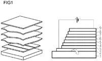
- the FIG. 1 shows the schematic layer structure of an organic radiation-emitting component. From bottom to top, the following layer structure is realized: At the bottom is the substrate 1, which may be transparent, for example, and may also be made of glass. On top of this there is a lower electrode layer 2, which may be, for example, a transparent conductive oxide such as indium tin oxide (ITO). The lower electrode layer can act as an anode or as a cathode. Overlying this electrode layer 2 is a hole injection layer 3 over which in turn a hole transport layer 4 is arranged. Above the hole transport layer 4, the organically active layer, the emission layer 5, is arranged.
- ITO indium tin oxide
- the radiation-emitting device contains more than one emission layer 5, then the further emission layers, which are optionally separated by exciton blocking layers, follow on the first emission layer.
- the upper electrode 9 may be, for example, a metal electrode or another transparent electrode, for example, one of the above-mentioned transparent conductive oxides.
- one or more phosphorescent exciton scavengers and one or more fluorescent radiation-emitting emitters are provided in the emission layer 5 in a matrix.
- an ITO layer is first deposited as an anode on a glass plate.
- this substrate is introduced into a recipient; it contains several sources in which organic material (in particular for use as exciton scavengers as well as for use as radiation-emitting emitters) can be vaporized to produce the individual functional layers of the radiation-emitting device.
- organic material in particular for use as exciton scavengers as well as for use as radiation-emitting emitters
- one or more sources are provided for the delivery of one or more different matrix materials.
- a source with matrix material and a source with a P-dopant are deposited together on the glass plate on which the anode is already present.
- the common deposition of dopant and matrix material for the hole transport layer takes place.
- the deposition of the emitter layer according to the invention takes place.
- a matrix material, the exciton scavenger and the at least one radiation-emitting emitter material are deposited together.
- matrix material, exciton scavenger and emitter material are deposited simultaneously.
- emitter material and exciton scavengers are not deposited simultaneously (not part of the present invention).
- matrix material and fluorescent emitters can be deposited simultaneously (first sub-layer), subsequently phosphorescent exciton scavengers and matrix material (second sub-layer), and finally matrix material and fluorescent emitters (third sub-layer).
- the deposition of further contained layers such as blocking layer, electron transport layer and electron injection layer is analogous.
- an aluminum layer is formed as a reflective electrode.
- the various functional layers can also be applied by means of a wet process (eg spin coating), this may be particularly useful if the layer to be applied contains a polymer.
- the layers applied first by means of a wet process and all layers arranged thereon can also be applied by vapor deposition.
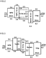
- the blue light-emitting OLED has a hole transport layer of NPB, which is 30 nm thick, applied to the ITO anode.
- An exciton blocking layer of TAPC with a thickness of 10 nm is disposed on the hole transport layer to avoid transfer of the excitons from the emitter layer to the less efficient hole transport layer.
- On the cathode of LiF / Al a 30 nm thick electron transport layer of TPBi is arranged.
- a 10 nm thick layer of Bphen which acts as an exciton blocking layer and hole blocking layer.
- the emitter layer itself comprises the matrix material TCTA into which the blue phosphorescent exciton trap fac-Ir (cn-pmic) 3 (energy levels in the FIG.
- the emitter layer has a layer thickness of 30 nm.
- the excitons are then first generated on the matrix material TCTA and transferred via the phosphorescent exciton trap Ir (pmb) 3 to the fluorescent emitter DPAVBi, where they can radiantly decay.
- the exciton scavenger is present in this embodiment in a concentration of 20 wt .-%; This results in a good direct exciton formation as well as a very good transfer of excitons formed on the matrix material to the exciton trap.
- the excitons are able to diffuse well over the exciton scavenger molecules to the fluorescent emitter molecules.
- the triplet level of the phosphorescent exciton trap (as well as that of the matrix) can be calculated from the emission wavelength of the phosphorescence (the matrix or the exciton trap).
- the singlet level of the fluorescent emitter can be determined by measuring the emission wavelength at room temperature.
- FIG. 3 shows a structure that the FIG. 2 corresponds; however, the emitter layer is formed by three sub-layers (not part of the present invention).
- the phosphorescent exciton scavenger fac-Ir (pmb) 3 is (in a concentration of 20% by weight) in the middle, 10 nm thick layer of the matrix material TCTA. Adjacent thereto are two 10 nm thick layers each with the fluorescent emitter DPAVBi.
- the sublayer adjoining the middle sublayer of the emitter layer on the anode side has the matrix material TAPC, while the sublayer adjacent thereto on the cathode side comprises the matrix material Bphen.
- excitons are formed on the matrix material TCTA (as well as on the exciton scavenger) and may then be in the direction of the interfaces to the respective adjacent sublayers, the excitons can not be delivered to the matrix material of the emitter emitter molecules, so that they are on be transferred to the singlet state of the fluorescent emitter and here can radiate decay.
Description
Die vorliegende Erfindung betrifft eine strahlungsemittierende Vorrichtung mit einer Emitterschicht, die ein Matrixmaterial, einen strahlungsemittierenden fluoreszierenden Emitter und einen Exzitonenfänger enthält. Diese Patentanmeldung beansprucht die Priorität der deutschen Patentanmeldung
Hoch effiziente Emitter mit möglichst langer Lebensdauer sind eine der Voraussetzungen für die Entwicklung hoch effizienter organischer lichtemittierender Dioden (OLEDs) sowie für Display- und Lightinganwendungen. Entscheidend für eine hohe Effizienz ist die Quanteneffizienz des einzelnen Emittermoleküls und die Quanteneffizienz des Emittersystems (aus Matrix und strahlungsemittierendem Emitter) insgesamt. Hohe Lebensdauern können aber nicht für alle emittierten Farben in gleichem Maß realisiert werden. Emitterschichten, die im violetten oder blauen Spektralbereich Licht emittieren, weisen deutlich kürzere Lebensdauern auf, als Emitterschichten die im grünen, gelben, orangen oder roten Spektralbereich emittieren. Dies gilt insbesondere für phosphoreszente Emitter. Eine OLED mit einem blauen fluoreszierendem Emitter wird in der
Aufgabe der Erfindung ist es, eine strahlungsemittierende Vorrichtung bereitzustellen, die eine im violetten oder blauen Spektralbereich Licht emittierende Emitterschicht verbesserter Quanteneffizienz und erhöhter Lebensdauer aufweist.The object of the invention is to provide a radiation-emitting device which has an emitter layer of improved quantum efficiency and increased lifetime which emits light in the violet or blue spectral region.
Diese Aufgabe wird durch die Vorrichtung gemäß dem unabhängigen Anspruch 1 gelöst. Weitere Ausgestaltungen sind Gegenstand von Unteransprüchen.This object is achieved by the device according to independent claim 1. Further embodiments are the subject of dependent claims.
Die erfindungsgemäße strahlungsemittierende Vorrichtung umfasst ein Substrat, eine erste Elektrode und eine zweite Elektrode sowie eine zwischen der ersten und der zweiten Elektrode angeordnete Emitterschicht, die (im Betrieb) Licht im violetten und/oder blauen Spektralbereich emittiert. Diese Emitterschicht enthält zum einem 0,1 bis 5 Gew.-% eines fluoreszierenden strahlungsemittierenden Emitters (der im violetten oder blauen Spektralbereich emittiert) und 1 bis 30 Gew.-% eines phosphoreszenten Exzitonenfängers. Neben dem fluoreszierenden strahlungsemittierenden Emitter und dem phosphoreszenten Exzitonenfänger weist die Emitterschicht ein Matrixmaterial auf (auf das sich die Angaben in Gew.-% beziehen). Im Regelfall ist der Gewichtsanteil des Exzitonenfängers größer als der des fluoreszierenden Emitters. Das Emissionsmaximum des fluoreszierenden Emitters liegt im blauen oder violetten Spektralbereich, das des phosphoreszenten Exzitonenfängers im blauen, violetten oder ultravioletten Spektralbereich.The radiation-emitting device according to the invention comprises a substrate, a first electrode and a second electrode, and an emitter layer arranged between the first and the second electrode, which emits (in operation) light in the violet and / or blue spectral range. This emitter layer contains from 0.1 to 5% by weight of a fluorescent radiation-emitting emitter (which emits in the violet or blue spectral region) and from 1 to 30% by weight of a phosphorescent exciton scavenger. In addition to the fluorescent radiation-emitting emitter and the phosphorescent exciton scavenger, the emitter layer has a matrix material (to which the data in% by weight relate). As a rule, the weight fraction of the exciton trap is greater than that of the fluorescent emitter. The emission maximum of the fluorescent emitter lies in the blue or violet spectral range, that of the phosphorescent exciton scavenger in the blue, violet or ultraviolet spectral range.
Durch die erfindungsgemäße Emitterschicht, die neben dem Matrixmaterial und dem fluoreszierenden Emitter auch einen phosphoreszenten Exzitonenfänger umfasst, ist es möglich, die Quanteneffizienz und die Leistungseffizienz zu verbessern. Im Regelfall bewirkt die Anwesenheit des phosphoreszenten Exzitonenfängers und des fluoreszierenden Emitters auch ein besseres Ladungsträgergleichgewicht und eine geringere Spannung - also eine verbesserte Stromeffizienz.The emitter layer according to the invention, which also comprises a phosphorescent exciton trap in addition to the matrix material and the fluorescent emitter, makes it possible to improve the quantum efficiency and the power efficiency. As a rule, the presence of the phosphorescent exciton trap and the fluorescent emitter also causes a better charge carrier balance and a lower voltage - ie an improved current efficiency.
Im Folgenden werden die einzelnen Komponenten der strahlungsemittierenden Vorrichtung der vorliegenden Erfindung näher erläutert:
Ein "Substrat" umfasst gemäß der vorliegenden Erfindung zum Beispiel ein Substrat, wie es im Stand der Technik herkömmlich für eine strahlungsemittierende Vorrichtung verwendet wird. Beispielsweise kann das Substrat Glas, Quarz, Kunststofffolien, Metall, Metallfolien, Siliziumwafer oder ein anderes geeignetes Substratmaterial umfassen. Ist die strahlungsemittierende Vorrichtung zum Beispiel als so genannter "Bottom-Emitter" ausgeführt, ist das Substrat vorzugsweise transparent und beispielsweise als Glassubstrat ausgeführt. In der erfindungsgemäßen strahlungsemittierenden Vorrichtung kann die erste Elektrode auf dem Substrat abgeschieden sein.The individual components of the radiation-emitting device of the present invention are explained in more detail below:
For example, a "substrate" in accordance with the present invention comprises a substrate conventionally used in the art for a radiation-emitting device. For example, the substrate glass, quartz, plastic films, metal, metal foils, silicon wafers or comprise another suitable substrate material. If the radiation-emitting device is designed, for example, as a so-called "bottom emitter", the substrate is preferably transparent and designed, for example, as a glass substrate. In the radiation-emitting device according to the invention, the first electrode may be deposited on the substrate.
Die "erste Elektrode", wie sie hierin verwendet wird, kann zum einen eine Anode sein. Die Anode kann aus einem löcherinjizierenden Material bestehen. Als löcherinjizierendes Material kann jedes im Stand der Technik bekannte, löcherinjizierende Material verwendet werden. Ist die strahlungsemittierende Vorrichtung beispielsweise als "Bottom-Emitter" ausgebildet, so besteht die Anode üblicherweise aus einem transparenten Material. Beispielsweise kann sie aus transparenten leitenden Oxiden bestehen oder eine Schicht hieraus umfassen. Diese transparenten leitenden Oxide (transparent conductive oxides, "TCO") schließen Metalloxide, wie beispielsweise Zinkoxid, Zinnoxid, Cadmiumoxid, Titanoxid, Indiumoxid oder Indiumzinnoxid (ITO), Zn2SnO4, CdSnO3, ZnSnO3, MgIn2O4, GaInO3, Zn2In2O5 oder In4Sn3O12 oder Mischungen unterschiedlicher transparenter leitender Oxide ein, sind jedoch nicht auf diese beschränkt. Die TCOs unterliegen dabei nicht zwingend einer stöchometrischen Zusammensetzung und können ferner auch p- oder n-dotiert sein.The "first electrode" as used herein may be an anode on the one hand. The anode may consist of a hole-injecting material. As hole injecting material, any hole injecting material known in the art can be used. If the radiation-emitting device is designed, for example, as a "bottom emitter", then the anode usually consists of a transparent material. For example, it may consist of transparent conductive oxides or comprise a layer thereof. These transparent conductive oxides ("TCOs") include metal oxides such as zinc oxide, tin oxide, cadmium oxide, titanium oxide, indium oxide or indium tin oxide (ITO), Zn 2 SnO 4 , CdSnO 3 , ZnSnO 3 , MgIn 2 O 4 , GaInO 3 , Zn 2 In 2 O 5 or In 4 Sn 3 O 12 or mixtures of different transparent conductive oxides, but are not limited to these. The TCOs are not necessarily subject to a stoichiometric composition and may also be p- or n-doped.
Wenn die erste Elektrode eine Anode ist, ist die zweite Elektrode eine Kathode. Die "Kathode" kann aus einem elektroneninjizierenden Material bestehen. Als Kathodenmaterialien können dabei im Stand der Technik übliche Kathodenmaterialien, insbesondere Aluminium, Barium, Indium, Silber, Gold, Magnesium, Calcium oder Lithium sowie Verbindungen, und Legierungen dieser Stoffe und Gemische der vorgenannten Elemente, Verbindungen und/oder Legierungen verwendet werden. Alternativ oder zusätzlich können auch eines oder mehrere der bei den Anoden-Materialien genannten TCOs enthalten sein bzw. kann die Kathode auch vollständig aus einem dieser Materialien bestehen. Die Kathode kann damit auch transparent ausgeführt sein.When the first electrode is an anode, the second electrode is a cathode. The "cathode" may consist of an electron-injecting material. Conventional cathode materials, in particular aluminum, barium, indium, silver, gold, magnesium, calcium or lithium as well as compounds and alloys of these substances and mixtures of the aforementioned elements, compounds and / or alloys can be used as cathode materials. Alternatively or additionally, too one or more of the TCOs mentioned in the anode materials may be contained or the cathode may also consist entirely of one of these materials. The cathode can thus be made transparent.
In der strahlungsemittierenden Vorrichtung kann zum Beispiel eine Elektrode transparent und die andere reflektierend ausgeführt sein. Die strahlungsemittierende Vorrichtung kann somit entweder als "Bottom-Emitter" oder als "Top-Emitter" ausgeführt werden. Alternativ dazu können auch beide Elektroden transparent ausgeführt sein.In the radiation-emitting device, for example, one electrode may be transparent and the other reflective. The radiation-emitting device can thus be embodied either as a "bottom emitter" or as a "top emitter". Alternatively, both electrodes can be made transparent.
Die Emitterschicht der erfindungsgemäßen strahlungsemittierenden Vorrichtung bezeichnet eine funktionelle Schicht aus einem Matrixmaterial, das einen oder mehrere fluoreszierende Emitter und einen oder mehrere phosphoreszente Exzitonenfänger enthält beziehungsweise aus dem Matrixmaterial, dem mindestens einen Emitter und dem mindestens einen Exzitonenfänger besteht.The emitter layer of the radiation-emitting device according to the invention denotes a functional layer of a matrix material which contains one or more fluorescent emitters and one or more phosphorescent exciton scavengers or consists of the matrix material, the at least one emitter and the at least one exciton scavenger.
Bei dem phosphoreszenten Exzitonenfänger handelt es sich um eine Verbindung, auf die ein effizienter Energieübertrag vom Matrixmaterial möglich ist. Dem Exzitonenfänger kommt dann die Aufgabe zu, einen effizienten und schnellen Energieübertrag auf das Emittermaterial zu gewährleisten, d.h. Exzitonen auf dieses Emittermaterial zu übertragen. Obwohl der Exzitonenfänger eine phosphoreszente Verbindung ist, kommt es insbesondere nicht darauf an, dass der Exzitonenfänger Strahlung emittiert; vielmehr ist es wesentlich, dass der Exzitonenfänger einen guten Transport der Exzitonen (und möglichst auch der Ladungsträger) gewährleistet. Die als Exzitonenfänger verwendeten Materialien unterscheiden sich stets von den als Emitter eingesetzten Materialien.The phosphorescent exciton trap is a compound capable of efficient energy transfer from the matrix material. The excitatory scavenger then has the task of ensuring an efficient and rapid transfer of energy to the emitter material, i. Transfer excitons to this emitter material. In particular, although the exciton scavenger is a phosphorescent compound, it does not matter that the exciton scavenger emits radiation; rather, it is essential that the exciton trap ensures good transport of the excitons (and, if possible, the charge carriers). The materials used as exciton scavengers always differ from the materials used as emitters.
Erfindungsgemäß wurde beobachtet, dass auf den Matrixmolekülen (oder Exzitonenfängern) Exzitonen gebildet werden und die auf den Matrixmolekülen gebildeten Triplett-Exzitonen von den Exzitonenfängern "eingefangen" werden; die Exzitonen werden anschließend zum (Singulettzustand der) fluoreszierenden Emitter transferiert. Hierdurch können zumindest teilweise die Triplettexzitonen des phosphoreszenten Exzitonenfängers auf dem fluoreszierenden Emitter strahlend genutzt werden, ohne dass diese auf dem phosphoreszenten Emitter strahlend oder nicht strahlend rekombinieren. Erfindungsgemäß wurde also erkannt, dass sich mit der erfindungsgemäßen Emitterschicht die hohe Effizienz des phosphoreszenten (zum Beispiel im Blauen emittierenden) Exzitonenfängers mit der guten Langzeitstabilität des fluoreszierenden (insbesondere blauen) Emitters kombiniert werden können. Nach dem Stand der Technik werden dagegen entweder Emitterschichten mit phosphoreszenten Emittern verwendet, bei denen zwar eine hohe Quanteneffizienz zu verzeichnen ist, da auch die Triplettexzitonen strahlend rekombinieren können, die aber (im Fall der blauen Emitter) eine geringe Langzeitstabilität besitzen; andererseits werden Emitterschichten mit blau fluoreszierenden Emittern eingesetzt, die eine wesentlich höhere Langzeitstabilität besitzen als phosphoreszierende blaue Emitter, die aber eine deutliche geringere Quanteneffizienz aufweisen, da nur Singulettexzitonen auf diesen Emittermaterialien strahlend rekombinieren können.According to the invention, it has been observed that excitons are formed on the matrix molecules (or exciton scavengers) and the triplet excitons formed on the matrix molecules are "captured" by the exciton scavengers; the excitons are then transferred to the singlet state of the fluorescent emitters. As a result, at least in part, the triplet exciters of the phosphorescent exciton trap can be used in a radiating manner on the fluorescent emitter, without these radiating or not radiating recombining on the phosphorescent emitter. According to the invention, it was thus recognized that the high efficiency of the phosphorescent (for example, in the blue emitting) exciton trap can be combined with the good long-term stability of the fluorescent (in particular blue) emitter with the emitter layer according to the invention. On the other hand, according to the prior art, either emitter layers with phosphorescent emitters are used in which a high quantum efficiency can be observed since the triplet excitons can also radiantly recombine, but which (in the case of the blue emitters) have a low long-term stability; On the other hand, emitter layers are used with blue-emitting emitters, which have a much higher long-term stability than phosphorescent blue emitters, but have a significantly lower quantum efficiency, since only singlet excitons can radiantly recombine on these emitter materials.
Bei der diesem Exzitonentransfer zugrunde liegenden Transferkaskade wird also ein auf den Matrixmaterial oder dem phosphoreszenten Exzitonenfänger generiertes Triplettexziton letztendlich auf den Singulettzustand des fluoreszierenden Emitters übertragen. Dies ist insbesondere aufgrund der Tatsache möglich, dass aufgrund der Spinn-Bahn-Kopplung Exzitonen generell eine Mischung aus Triplett- und SingulettZustand darstellen. Erfindungsgemäß eignen sich insbesondere "Triplett-Exzitonen" mit einer Zerfallszeit < 10 µs für einen Transfer auf das Singulettniveau des fluoreszierenden Emitters.Thus, in the transfer cascade underlying this exciton transfer, a triplet exciton generated on the matrix material or the phosphorescent exciton scavenger is ultimately transferred to the singlet state of the fluorescent emitter. This is possible in particular because of the fact that due to the spin-orbit coupling, excitons generally represent a mixture of triplet and singlet states. According to the invention, in particular "triplet excitons" with a disintegration time <10 μs are suitable for a transfer to the singlet level of the fluorescent emitter.
Durch die höhere Konzentration des Exzitonenfänger wird ein effizienter Energieübertrag auf die fluoreszierenden Emitter gewährleistet. Durch die niedrigere Konzentration des Emitters kann dagegen verhindert werden, dass, insbesondere bei Emittern ohne sterische Hinderung, eine Stapelung der Moleküle auftritt, welche eine Rotverschiebung des emittierten Spektrums zur Folge haben kann. Die hohen Konzentrationen des Exzitonenfängers bewirken dagegen - neben den vorstehenden Effekten, dass diese Exzitonenfänger nicht als Fallenzentren für die Ladungsträger wirken; im Gegenteil, es kann ein guter Transport der Ladungsträger stattfinden.The higher concentration of the exciton trap ensures an efficient transfer of energy to the fluorescent emitters. On the other hand, the lower concentration of the emitter makes it possible to prevent, especially in the case of emitters without steric hindrance, a stacking of the molecules, which can result in a redshift of the emitted spectrum. The high concentrations of the exciton scavenger, on the other hand, cause, in addition to the above effects, that these exciton scavengers do not act as trap centers for the charge carriers; on the contrary, a good transport of the charge carriers can take place.
Insbesondere kann ein Ladungsträgertransport erfolgen, indem die Matrix die Majoritätsladungsträger transportiert und der Exzitonenfänger die Minoritätsladungsträger mit entgegengesetzter Ladung (z. B. werden bei einer lochtransportierenden Matrix die Elektronen über das LUMO des Exzitonenfängers transportiert). Die erfindungsgemäße strahlungsemittierende Vorrichtung weist daher im Regelfall auch eine verbesserte Stromeffizienz auf. Oft ist die Stromeffizienz (verglichen mit Emitterschichten ohne Exzitonenfänger) auf um mindestens 10% erhöht. Häufig liegt die Stromeffizienz sogar 20% und vielfach sogar 25% über der Stromeffizienz einer entsprechenden Emitterschicht ohne den erfindungsgemäßen Exzitonenfänger. Dies gilt insbesondere für Stromeffizienzen bei hohen Lichtstärken, d.h. Lichtstärken, die typischerweise größer 1000 cd/m2 sind.In particular, a charge carrier transport can take place in that the matrix transports the majority charge carriers and the exciton trap transports the minority charge carriers of opposite charge (for example, in the case of a hole-transporting matrix, the electrons are transported via the LUMO of the exciton trap). As a rule, the radiation-emitting device according to the invention therefore also has an improved current efficiency. Often the current efficiency (compared to emitter layers without exciton trap) is increased by at least 10%. Often the current efficiency is even 20% and often even 25% higher than the current efficiency of a corresponding emitter layer without the exciton scavenger according to the invention. This applies in particular to current efficiencies at high light intensities, ie light intensities which are typically greater than 1000 cd / m 2 .
Zusammenfassend kann festgestellt werden, dass erfindungsgemäß erkannt wurde, dass durch die Kombination eines phosphoreszenten Exzitonenfängers in hoher Konzentration und eines Emittermaterials in niedrigerer Konzentration unabhängig voneinander zwei Effekte realisiert werden können. Zum einen werden durch dieses gemischte System im Betrieb zunächst Exzitonen vom Matrixmaterial auf den Exzitonenfänger übertragen beziehungsweise auf dem Exzitonenfänger gebildet. Durch einen effizienten und schnellen Energieübertrag werden dann die Triplett-Exzitonen auf das Singulett-Niveau des fluoreszierenden Emitters (mit gegenüber dem phosphoreszenten Exitonenfänger erhöhter Lebensdauer) übertragen, auf dem strahlend zerfallen können. Außerdem weist der Exzitonenfänger hervorragende Leitungseigenschaften für die Minoritätsladungsträger auf. Beide Effekte führen insgesamt zu einer deutlich erhöhten Quanteneffizienz und daneben auch zu einem besseren Ladungsträgergleichgewicht und zu einer geringeren Spannung.In summary, it can be stated that it has been recognized according to the invention that two effects can be realized independently of one another by combining a phosphorescent exciton trap in high concentration and an emitter material in a lower concentration. On the one hand, excitons are initially transferred from the matrix material to the exciton trap or formed on the exciton trap during operation by this mixed system. Through an efficient and the triplet excitons are then transferred to the singlet level of the fluorescent emitter (with an increased lifespan compared to the phosphorescent exiton trap) on which rapid energy transfer can occur, on which radiant decay can occur. In addition, the exciton scavenger has excellent minority carrier conduction properties. Overall, both effects lead to a significantly increased quantum efficiency and, in addition, to a better charge carrier equilibrium and to a lower voltage.
Der fluoreszierende Emitter und der Exzitonenfänger können jeweils in ein Matrixmaterial eingebettet sein, das beispielsweise ausgewählt ist aus der Gruppe, bestehend aus mCP (1,3-Bis(carbazol-9-yl)benzol), TCP (1,3,5-Tris(carbazol)-9-yl)benzol), TCTA (4,4',4''-Tris(carbazol-9-yl)triphenylamin), TPBi (1,3,5-tris(1-phenyl-1-H-benzimidazol-2-yl)benzol), CBP (4,4'-Bis(carbazol-9-yl)biphenyl), CDBP (4,4'-Bis(9-carbazolyl)-2,2'-dimethylbiphenyl), (DMFL-CBP 4,4'-Bis(carbazol-9-yl)-9,9-dimethylfluoren), FL-4CBP (4,4'-Bis(carbazol-9-yl)-9,9-bis(9-phenyl-9H-carbazol)fluoren), FL-2CBP (9,9-Bis(4-carbazol-9-yl)-phenyl)fluoren, auch abgekürzt als CPF), DPFL-CBP (4,4'-Bis(carbazol-9-yl)-9,9-ditolylfluoren), FL-2CBP (9,9-Bis(9-phenyl-9H-carbazol)fluoren), Spiro-CBP (2,2',7,7'-Tetrakis(carbazol-9-yl)-9,9'-spiro-bifluoren), ADN (9,10-Di(naphth-2-yl)anthracen, TBADN (3-Tert-butyl-9,10-di(naphth-2-yl)anthracen, DPVBi (4,4'-Bis(2,2-diphenyl-ethen-1-yl)-4,4'-dimethylphenyl), p-DMDPVBi (4,4'-Bis(2,2-diphenyl-ethen-1-yl)-4,4'-dimethylphenyl), TDAF (Tert(9,9-diarylfluoren)), BSBF (2-(9,9'-Spirobifluoren-2-yl)-9,9'-spirobifluoren), TSBF (2,7-Bis(9,9'-spirobifluoren-2-yl)-9,9'-spirobifluoren), BDAF Bis(9,9-diarylfluoren), p-TDPVBi (4,4'-Bis(2,2-diphenylethen-1-yl)-4,4'-di-(tert-butyl)phenyl), TPB3 (1,3,5-Tri-(pyren-1-yl)benzol), PBD (2-(4-Biphenylyl)-5-(4-tert-butylphenyl)-1,3,4-oxadiazol), BCP (2,9-Dimethyl-4,7-diphenyl-1,10-phenanthrolin), BP-OXD-Bpy (6,6'-Bis[5-(biphenyl-4-yl)-1,3,4-oxadiazo-2-yl]-2,2'-bipyridyl), NTAZ (4-(Naphth-1-yl)-3,5-diphenyl-4H-1,2,4-triazol), Bpy-OXD (1,3-Bis[2-(2,2'-bipyrid-6-yl)-1,3,4-oxadiazo-5-yl]benzol), BPhen (4,7-Diphenyl-1,10-phenanthrolin), TAZ (3-(4-Biphenylyl)-4-phenyl-5-tert-butylphenyl-1,2,4-triazol), PADN (2-phenyl-9,10-di(naphth-2-yl)-anthracen), Bpy-FOXD (2,7-Bis[2-(2,2'-bipyrid-6-yl)-1,3,4-oxadiazol-5-yl]-9,9-dimethylfluoren), OXD-7 (1,3-Bis[2-(4-tert-butylphenyl)-1,3,4-oxadiazol-5-yl]benzol), HNBphen (2-(naphth-2-yl)-4,7-diphenyl-1,10-phenanthrolin), NBphen (2,9-Bis(naphth-2-yl)-4,7-diphenyl-1,10-phenanthrolin), 3TPYMB (Tris(2,4,6-trimethyl-3-(pyrid-3-yl)phenyl)boran), 2-NPIP (1-methyl-2-(4-(naphth-2-yl)phenyl)-1H-imidazo[4,5-f] [1,10]phenanthrolin), Liq (8-Hydroxychinolinolato-lithium) und Alq (Bis(2-methyl-8-chinolinolat)-4-(phenylphenolato)aluminium) sowie aus Gemischen der vorgenannten Stoffe. Als Matrixmaterial bevorzugt sind aromatische Materialien mit hohem Stickstoffanteil, etwa die Materialen mCP, TCTA, TPBi, BCP, BPhen, CBP, CDBP und CPF (d.h. FL-2CBP) oder Metallkomplexe, etwa Alq. Bei der Verwendung von Metallkomplexen als Matrixmaterial, dürfen diese nicht mit dem Emittermaterial (oder dem Exzitonenfänger) übereinstimmen. Als Matrixmaterialien die in gemischten System vorliegen, eignen sich beispielsweise Mischungen aus einem oder mehreren der Materialien TCTA, mCP, CBP, CDBP oder CPF untereinander oder Mischungen mit TPBi verwendet.Each of the fluorescent emitter and the exciton scavenger may be embedded in a matrix material selected, for example, from the group consisting of mCP (1,3-bis (carbazol-9-yl) benzene), TCP (1,3,5-tris (carbazole) -9-yl) benzene), TCTA (4,4 ', 4 "-tris (carbazol-9-yl) triphenylamine), TPBi (1,3,5-tris (1-phenyl-1-H benzimidazol-2-yl) benzene), CBP (4,4'-bis (carbazol-9-yl) biphenyl), CDBP (4,4'-bis (9-carbazolyl) -2,2'-dimethylbiphenyl), (DMFL-CBP 4,4'-bis (carbazol-9-yl) -9,9-dimethylfluorene), FL-4CBP (4,4'-bis (carbazol-9-yl) -9,9-bis (9th to 9th)) -phenyl-9H-carbazole) fluorene), FL-2CBP (9,9-bis (4-carbazol-9-yl) -phenyl) fluorene, also abbreviated as CPF), DPFL-CBP (4,4'-bis ( carbazol-9-yl) -9,9-ditolylfluorene), FL-2CBP (9,9-bis (9-phenyl-9H-carbazole) fluorene), spiro-CBP (2,2 ', 7,7'-tetrakis (carbazol-9-yl) 9,9'-spirobifluorene), ADN (9,10-di (naphth-2-yl) anthracene, TBADN (3-tert-butyl-9,10-di (naphthenic) 2-yl) anthracene, DPVBi (4,4'-bis (2,2-diphenyl-ethen-1-yl) -4,4'-dimethylphenyl), p-DMDPVBi (4,4'-bis (2,2 -di phenyl-ethen-1-yl) -4,4'-dimethylphenyl), TDAF (tert (9,9-diarylfluorene)), BSBF (2- (9,9'-spirobifluoren-2-yl) -9.9 ' -spirobifluorene), TSBF (2,7-bis (9,9'-spirobifluoren-2-yl) -9,9'-spirobifluorene), BDAF bis (9,9-diarylfluorene), p-TDPVBi (4,4 '). Bis (2,2-diphenylethen-1-yl) -4,4'-di (tert-butyl) phenyl), TPB3 (1,3,5-tri (pyrene-1-yl) benzene), PBD (2- (4-biphenylyl) -5- (4-tert-butylphenyl) -1,3,4-oxadiazole), BCP (2,9-dimethyl-4,7-diphenyl-1,10-phenanthroline), BP -OXD-Bpy (6,6'-bis [5- (biphenyl-4-yl) -1,3,4-oxadiazol-2-yl] -2,2'-bipyridyl), NTAZ (4- (naphth-1-yl) -3,5-diphenyl-4H-1,2,4-triazole), Bpy-OXD (1,3-bis [2- (2,2'-bipyrid-6-) yl) -1,3,4-oxadiazo-5-yl] benzene), BPhen (4,7-diphenyl-1,10-phenanthroline), TAZ (3- (4-biphenylyl) -4-phenyl-5-tert -butylphenyl-1,2,4-triazole), PADN (2-phenyl-9,10-di (naphth-2-yl) -anthracene), Bpy-FOXD (2,7-bis [2- (2,2 '-bipyrid-6-yl) -1,3,4-oxadiazol-5-yl] -9,9-dimethylfluorene), OXD-7 (1,3-bis [2- (4-tert-butylphenyl) -1 , 3,4-oxadiazol-5-yl] benzene), HNBphen (2- (naphth-2-yl) -4,7-diphenyl-1,10-phenanthroline), NBphen (2,9-bis (naphth-2 -yl) -4,7-diphenyl-1,10-phenanthroline), 3TPYMB (tris (2,4,6-trimethyl-3- (pyrid-3-yl) phenyl) borane), 2-NPIP (1-methyl -2- (4- (naphth-2-yl) phenyl) -1H-imidazo [4,5-f] [1,10] phenanthroline), Liq (8-hydroxyquinolinolato-lithium) and Alq (bis (2-methyl -8-quinolinolate) -4- (phenylphenolato) aluminum) and from mixtures of the abovementioned substances. Preferred as the matrix material are high nitrogen content aromatic materials, such as mCP, TCTA, TPBi, BCP, BPhen, CBP, CDBP and CPF (ie, FL-2CBP) or metal complexes, such as Alq. When using metal complexes as matrix material, they must not match the emitter material (or the exciton trap). As matrix materials which are present in mixed systems, for example mixtures of one or more of the materials TCTA, mCP, CBP, CDBP or CPF with one another or mixtures with TPBi are used.
Ein blau phosphoreszierender Exzitonenfänger kann ausgewählt sein aus der Gruppe, bestehend aus FIrPic (Bis(3,5-difluoro-2-(2-pyridyl)phenyl-(2-carboxypyridyl)-iridium III), FIr6 (Bis(48,68-difluorophenylpyridinato)-tetrakis (1-pyrazolyl)borat-iridium III), mer-Ir(dpbic)3 (mer-Iridium(III) tris(1,3-diphenyl-benzimidazolin-2-yliden-C,C2')), mer-Ir(cn-pmic)3 (mer-Iridium(III) tris(1-methyl-3-p-cyanophenyl-imidazolin-2-yliden-C,C2')), mer-Rh(cn-pmic)3 (mer-Rhodium(III) tris(1-methyl-3-p-cyanophenyl-imidazolin-2-yliden-C,C2')), Pt(cn-pmic)acac (Platin(II) (1-methyl-3-p-cyanophenyl-imidazolin-2-yliden-C,C2')acetylacetonat) sowie aus Gemischen der vorgenannten Stoffe. Die vier zuletzt genannten Stoffe sind in
Ein blau phosphoreszierender Exzitonenfänger kann ausgewählt sein aus der Gruppe, bestehend aus fac-Ir(Pmb)3 (fac-Iridium(III) tris(1-phenyl-3-methylbenzimidazolin-2-yliden-C,C2')), mer-Ir(Pmb)3 (mer-Iridium(III) tris(1-phenyl-3-methylbenzimidazolin-2-yliden-C,C2')), fac-Ir(dpbic)3 (fac-Iridium(III) tris(1,3-diphenyl-benzimidazolin-2-yliden-C,C2') -
Als fluoreszierender Emitter kann eine Verbindung eingesetzt werden, die das Emissionsmaximum im violetten oder blauen Spektralbereich aufweist. Das Emissionsspektrum des Emitters kann weitere Maxima aufweisen; im Regelfall werden diese aber auch im blauen und/oder violetten Spektralbereich liegen. Als blau fluoreszierender Emitter kann beispielsweise eine Verbindung eingesetzt werden die ausgewählt ist aus der Gruppe, bestehend aus BCzVBi (4,4'-Bis(9-ethyl-3-carbazovinylen)-1,1'-biphenyl), Perylen, TBPe (2,5,8,11-Tetra-tert-butylperylen), BCzVB (9H-Carbazol-3,3'-(1,4-phenylen-di-2,1-ethendiyl)bis[9-ethyl-(9C)]), DPAVBi 4,4-Bis[4-(di-p-tolylamino)styryl]biphenyl, DPAVB (4-(Di-p-tolylamino)-4'-[(di-p-tolylamino)styryl]stilben), BDAVBi (4,4'-Bis[4-(diphenylamino)styryl]biphenyl), BNP3FL (N,N'-Bis(naphthalen-2-yl)-N,N'-bis (phenyl)-tris-(9,9-dimethylfluorenylen), 9,10-Bis[(9-ethyl-3-carbazoyl)-vinylenyl]-anthracen, 4,4'-Bis(diphenylvinylenyl)-biphenyl, 1,4-Bis(9-ethyl-3-carbazovinylen)-2-methoxy-5-(2-thylhexyloxy)benzol, 4,4'-Bis(diphenylvinylenyl)-anthracen, 1,4-Bis(9-ethyl-3-carbazovinylen)-9,9-dihexyl-fluoren sowie aus Gemischen der vorgenannten Stoffe. Die genannten Emittermaterialien haben ihr Emissionsmaximum im blauen Spektralbereich.As a fluorescent emitter, a compound can be used which has the emission maximum in the violet or blue spectral range. The emission spectrum of the emitter can have more maxima; As a rule, however, these will also be in the blue and / or violet spectral range. As the blue fluorescent emitter, for example, a compound selected from the group consisting of BCzVBi (4,4'-bis (9-ethyl-3-carbazovinylene) -1,1'-biphenyl), perylene, TBPe (2 , 5,8,11-tetra-tert-butylperylene), BCzVB (9H-carbazole-3,3 '- (1,4-phenylene-di-2,1-ethendiyl) bis [9-ethyl- (9C)] DPAVBi 4,4-bis [4- (di-p-tolylamino) styryl] biphenyl, DPAVB (4- (di-p-tolylamino) -4 '- [(di-p-tolylamino) styryl] stilbene), BDAVBi (4,4'-bis [4- (diphenylamino) styryl] biphenyl), BNP3FL (N, N'-bis (naphthalen-2-yl) -N, N'-bis (phenyl) -tris- (9, 9-dimethylfluorenylene), 9,10-bis [(9-ethyl-3-carbazoyl) -vinylenyl] -anthracene, 4,4'-bis (diphenylvinylenyl) -biphenyl, 1,4-bis (9-ethyl-3-) carbazovinylene) -2-methoxy-5- (2-thylhexyloxy) benzene, 4,4'-bis (diphenylvinylenyl) -anthracene, 1,4-bis (9-ethyl-3-carbazovinylene) -9,9-dihexyl-fluorene and mixtures of the abovementioned substances. The emitter materials mentioned have their emission maximum in the blue spectral range.
In einer nicht erfinderischen Ausführungsform ist die Emitterschicht in mindestens zwei Teilschichten unterteilt. Sie weist dabei zumindest eine erste Teilschicht (d. h. Teilschicht(en) eines ersten Typs) auf, bei der das Matrixmaterial nur den fluoreszierenden strahlungsemittierenden Emitter aber keinen phosphoreszenten Exzitonenfänger enthält. Ferner weist die Emitterschicht dann zumindest eine zweite Teilschicht (d. h. Teilschicht(en) eines zweiten Typs) auf, bei der das Matrixmaterial nur den phosphoreszenten Exzitonenfänger aber keinen fluoreszierenden strahlungsemittierenden Emitter enthält.In a non-inventive embodiment, the emitter layer is subdivided into at least two partial layers. It has at least a first part-layer (i.e., sub-layer (s) of a first type) in which the matrix material contains only the fluorescent radiation-emitting emitter but no phosphorescent exciton-trap. Further, the emitter layer then comprises at least a second sub-layer (i.e., sub-layer (s) of a second type) in which the matrix material contains only the phosphorescent exciton scavenger but no fluorescent radiation-emitting emitter.
Bei einer derartigen Ausführungsform werden Triplettexzitonen zunächst auf dem Matrixmaterial (oder auch auf dem Exzitonenfänger) gebildet und auf den phosporeszenten Exzitonenfänger übertragen. Die Triplettexzitonen diffundieren dann in Richtung der Grenzfläche zwischen erster und zweiter Teilschicht und werden schließlich auf den fluoreszierenden Emitter übertragen.In such an embodiment, triplet excitons are first formed on the matrix material (or on the exciton scavenger) and transferred to the phosporescent exciton scavenger. The triplet excitons then diffuse toward the interface between the first and second sublayers and are finally transferred to the fluorescent emitter.
In einer nicht erfinderischen Variante befindet sich dabei eine Teilschicht, die (nur) den phosphoreszenten Exzitonenfänger enthält zwischen zwei Teilschichten, die jeweils (nur) den fluoreszierenden Emitter enthalten. In diesem Fall können die Triplettexzitonen von den Molekülen des phosphoreszenten Exzitonenfängers ungerichtet in alle Richtungen diffundieren und treffen dennoch auf eine Grenzfläche zur anderen Teilschicht.In a non-inventive variant, there is a partial layer which contains (only) the phosphorescent exciton trap between two partial layers which each contain (only) the fluorescent emitter. In this case, the triplet excitons can diffuse non-directionally from the molecules of the phosphorescent exciton scavenger in all directions and yet strike an interface with the other sublayer.
Liegen mehrere Teilschichten vor, so kann das für die jeweiligen Teilschichten verwendete Matrixmaterial gleich oder verschieden sein. Häufig wird das Matrixmaterial, das den phosphoreszenten Exzitonenfänger enthält bezüglich des Triplett-Niveaus auf das Triplett-Niveau des Exzitonenfängers abgestimmt sein. Eine kathodenseitig an die den Exzitonenfänger enthaltende Teilschicht angrenzende Teilschicht kann beispielsweise als Matrixmaterial das selbe Material aufweisen, wie eine wiederum kathodenseitig an diese Teilschicht angrenzende Lochblockier-Schicht, Elektronentransport-Schicht oder ElektronenInjektionsschicht. Eine anodenseitig an die den phosphoreszierenden Exzitonenfänger angrenzende Teilschicht kann zum Beispiel das selbe Matrixmaterial aufweisen, wie eine wiederum kathodenseitig an diese Teilschicht angrenzende Elektronenblockier-Schicht, Lochtransport-Schicht oder Lochinjektions-Schicht. Alternativ kann natürlich das Matrixmaterial der Teilschicht beziehungsweise der Teilschichten, die den fluoreszierenden Emitter enthalten, auch aus einem Matrixmaterial bestehen, das zwar nicht dem zuvor beschriebenen kathodenseitig beziehungsweise anodenseitig an diese Teilschichten angrenzenden Matrixmaterial entspricht, aber aus den vorstehend angegebenen Matrixmaterialien ausgewählt ist. Dem entsprechend ist insbesondere für eine kathodenseitig angeordnete Teilschicht mit fluoreszentem Emitter jegliches lochblockierende und Elektronen transportierende Matrixmaterial geeignet, für eine anodenseitig angeordnete Teilschicht mit fluoreszierenden Emittern jegliches elektronenblockierende und lochtransportierende Matrixmaterial. In beiden Fällen kann das Matrixmaterial zudem so ausgewählt sein, dass es auch exzitonenblockierende Eigenschaften besitzt. Dies hat den Effekt, dass in der Teilschicht, die den Exzitonenfänger enthält, gebildete Exzitonen nicht auf das Matrixmaterial der Teilschicht mit den fluoreszierenden Emitter übertragen werden kann, sondern im Wesentlichen nur auf das Singulett-Niveau des fluoreszierenden Emitters übertragen wird und hier (in Nähe der Grenzfläche zwischen den Teilschichten) strahlend zerfallen kann.If several partial layers are present, then the matrix material used for the respective partial layers can be the same or different. Often, the matrix material containing the phosphorescent exciton scavenger will be tuned to the triplet level of the exciton trap with respect to the triplet level. A partial layer adjoining the partial layer containing the exciton trap on the cathode side can have, for example, the same material as a matrix material, such as a hole blocking layer, electron transport layer or electron injection layer adjacent to this partial layer on the cathode side. An anode side adjacent to the phosphorescent excitement scavenger sub-layer may for example comprise the same matrix material as a turn on the cathode side adjacent to this sub-layer electron-blocking layer, hole transport layer or hole injection layer. Alternatively, of course, the matrix material of the sub-layer or the sub-layers containing the fluorescent emitter may also consist of a matrix material that does not correspond to the previously described cathode material on the anode side or anode side adjacent to these sub-layers, but is selected from the matrix materials mentioned above. the Correspondingly, any hole-blocking and electron-transporting matrix material is suitable in particular for a sub-layer with a fluorescent emitter arranged on the cathode side, and any electron-blocking and hole-transporting matrix material for a sub-layer having fluorescent emitters arranged on the anode side. In either case, the matrix material may also be selected to also possess exciton-blocking properties. This has the effect that excitons formed in the sublayer containing the exciton scavenger can not be transferred to the matrix material of the fluorescent emitter sublayer, but is transferred substantially only to the singlet level of the fluorescent emitter and here (near the interface between the partial layers) can radiate decay.
In der erfinderischen Ausführungsform weist die Emitterschicht keine Teilschichten auf (die jeweils nur dem fluoreszierenden strahlungsemittierenden Emitter und das Matrixmaterial oder nur den phosphoreszenten Exzitonenfänger und das Matrixmaterial enthalten). In diesem Fall sind die Moleküle des phosphoreszenten Exzitonenfängers und die des fluoreszierenden Emitters statistisch über die gesamte Emitterschicht verteilt.In the inventive embodiment, the emitter layer has no sub-layers (each containing only the fluorescent radiation-emitting emitter and the matrix material or only the phosphorescent exciton scavenger and the matrix material). In this case, the molecules of the phosphorescent exciton trap and that of the fluorescent emitter are randomly distributed over the entire emitter layer.
Der fluoreszierende Emitter und auch der phosphoreszente Exzitonenfänger sind statistisch über das Matrixmaterial verteilt. In einer nicht erfinderischen Ausführungsform können auch Konzentrationsgradienten in der Emitterschicht vorliegen, so dass sich beispielsweise Bereiche, in denen der Exzitonenfänger höher konzentriert ist mit Bereichen, in denen der fluoreszierende Emitter im Verhältnis höher konzentriert ist, abwechseln; es können in der Emitterschicht sogar auch nur Bereiche vorliegen (die aber noch keine echte Teilschicht darstellen), in denen ausschließlich Exzitonenfänger enthalten ist und Bereiche in denen ausschließlich der phosphoreszente Emitter enthalten ist. Hiermit können gezielt Zonen eingestellt werden, in denen hauptsächlich Exzitonen gebildet werden beziehungsweise Zonen, in denen hauptsächlich die Emission erfolgt.The fluorescent emitter and also the phosphorescent exciton trap are statistically distributed over the matrix material. In a non-inventive embodiment, concentration gradients may also be present in the emitter layer, see above for example, areas where the exciton scavenger is more highly concentrated alternate with areas where the fluorescent emitter is relatively more concentrated; In the emitter layer, there may even be only regions (which, however, do not yet represent a true sublayer), in which exclusively exciton scavengers are contained and regions in which only the phosphorescent emitter is contained. This can be targeted zones are set in which mainly excitons are formed or zones in which mainly the emission takes place.
Generell können durch das erfindungsgemäße (Molekül-Verhältnis) zwischen fluoreszierenden strahlungsemittierendem Emitter und phosphoreszentem Exzitonenfänger nicht strahlende Konkurrenzprozesse wie beispielsweise eine direkte Bildung von Triplettexzitonen auf dem fluoreszierenden Dotierstoff oder eine Triplett-Triplett-Anihilation auf dem phosphoreszenten Exzitonenfänger minimiert werden.In general, non-radiative competing processes, such as, for example, direct formation of triplet excitons on the fluorescent dopant or triplet triplet annihilation on the phosphorescent exciton trap, can be minimized by the (molecular ratio) according to the invention between fluorescent radiation-emitting emitter and phosphorescent exciton trap.
In Ausführungsformen ist der Gewichtsanteil des phosphoreszenten Exzitonenfängers zumindest viermal, häufig sogar zumindest achtmal so hoch wie der des fluoreszierenden strahlungsemittierenden Emitters.In embodiments, the weight fraction of the phosphorescent exciton scavenger is at least four times, often even at least eight times, that of the fluorescent radiation-emitting emitter.
In einer weiteren Ausführungsform beträgt der Anteil des phosphoreszenten Exzitonenfängers 10 - 20 Gew.-% (im Rahmen der vorliegenden Erfindung beziehen sich alle Angaben in Gew.-% stets auf das in der Emitterschicht enthaltene Matrixmaterial). Ab einem Gewichtsanteil von mindestens 10 Gew.-% ist im Matrixmaterial so viel Exzitonenfänger enthalten, dass ein sehr effizienter Transport der Ladungsträger ermöglicht wird und daher ein deutlicher Anstieg der Stromeffizienz zu verzeichnen ist. Ab einem Anteil von 20 Gew.-% kann es unter Umständen verstärkt dazu kommen, dass durch Wechselwirkungen von zwei Exzitonen Effizienzverluste erfolgen.In a further embodiment, the proportion of the phosphorescent exciton scavenger is 10-20% by weight (in the context of the present invention, all data in% by weight always refer to the matrix material contained in the emitter layer). From a weight proportion of at least 10 wt .-% so much excitement scavenger is included in the matrix material that a very efficient transport of the charge carriers is made possible and therefore a significant increase in the power efficiency is recorded. From a proportion of 20% by weight, under certain circumstances it can increasingly occur that efficiency losses occur through interactions of two excitons.
In einer weiteren Ausführungsform ist der Anteil des fluoreszierenden Emitters 1 - 4 Gew.-%. Ab einem Gewichtsanteil von 5 Gew.-% ist - abhängig vom jeweiligen Emitter - mit einem Konzentrationsquenching und daher einer deutlich sinkenden Effizienz zu rechnen.In a further embodiment, the proportion of the fluorescent emitter is 1 - 4 wt .-%. From a weight proportion of 5 wt .-% is - depending on the respective emitter - to expect a concentration quenching and therefore a significantly decreasing efficiency.
In einer Ausführungsform weist der phosphoreszente Exzitonenfänger das Emissionsmaximum bei einer kürzeren Wellenlänge auf als der strahlungsemittierende Emitter.In one embodiment, the phosphorescent exciton trap has the emission maximum at a shorter wavelength than the radiation-emitting emitter.
Dies gewährleistet im Regelfall, dass eine effiziente Energietransferkaskade vom phosphoreszenten Exzitonenfänger zum Singulettniveau des fluoreszierenden Emitters stattfinden kann. Insbesondere sollte das Triplettniveau des Matrixmaterials (T1Matrix) höher liegen als das Triplettniveau des Exzitonenfängers (T1Exzitonenfänger), das wiederum höher liegen muss als das Singulettniveau des fluoreszierenden Emitters (S1Emitter). Wie beschrieben, werden dann die Triplettexzitonen auf dem Matrixmaterial gebildet, auf den phosphoreszenten Exzitonenfänger übertragen, der die Triplett-Exzitonen dann auf den Singulettzustand des fluoreszierenden Emitters überträgt (und insbesondere nicht an das Matrixmaterial einer Teilschicht mit dem fluoreszierenden Emitter abgeben kann - sofern Teilschichten der Emitterschicht vorliegen und diese Teilschichten unterschiedliche Matrixmaterialien aufweisen).This usually ensures that an efficient energy transfer cascade from the phosphorescent exciton trap to the singlet level of the fluorescent emitter can take place. In particular, the triplet level of the matrix material (T1 matrix ) should be higher than the triplet level of the exciton trap (T1 exciton trap ), which in turn must be higher than the singlet level of the fluorescent emitter (S1 emitter ). As described, the triplet excitons are then formed on the matrix material, transferred to the phosphorescent exciton scavenger, which then transmits the triplet excitons to the singlet state of the fluorescent emitter (and in particular can not deliver to the matrix material of a sublayer with the fluorescent emitter - if partial layers of the Emitter layer present and these sublayers have different matrix materials).
In einer weiteren Ausführungsform beträgt die Differenz der Wellenlängen des Emissionsmaximums des strahlungsemittierenden Emitters und des Emissionsmaximums des Exzitonenfängers 1 nm bis 100 nm, bevorzugt zumindest 15 nm oder zumindest sogar 30 nm bis 100 nm. Dann ist im Regelfall ebenfalls eine effiziente Energietransferkaskade möglich.In a further embodiment, the difference between the wavelengths of the emission maximum of the radiation-emitting emitter and the emission maximum of the exciton trap is 1 nm to 100 nm, preferably at least 15 nm or at least even 30 nm to 100 nm. Then, as a rule, an efficient energy transfer cascade is also possible.
In einer weiteren Ausführungsform zeichnet sich die strahlungsemittierende Vorrichtung dadurch aus, dass die mittlere Lebensdauer der Emitterschicht (bei einer Leuchtdichte von 300 cd/m2) gegenüber der mittleren Lebensdauer einer strahlungsemittierenden Vorrichtung, die sich nur darin unterscheidet, dass die Emitterschicht nur den phosphoreszenten Exzitonenfänger (und nicht den fluoreszierenden Emitter) enthält, um mindestens 50 Prozent erhöht ist. Häufig kann sogar eine Erhöhung der mittleren Lebensdauer um 100 Prozent beobachtet werden. Auch Erhöhungen um bis zu 300 Prozent oder um bis zu 500 Prozent werden beobachtet.In a further embodiment, the radiation-emitting device is characterized in that the average life of the emitter layer (at a luminance of 300 cd / m 2 ) over the average life of a radiation-emitting device, differing only in that the emitter layer contains only the phosphorescent exciton trap (and not the fluorescent emitter) increased by at least 50 percent is. Often, even an increase in average life of 100 percent can be observed. Increases of up to 300 percent or up to 500 percent are also observed.
Die erfindungsgemäße strahlungsemittierende Vorrichtung weist dann (bei einer Leuchtdichte von 300 cd/m2) im Regelfall eine mittlere Lebensdauer von mindestens 10.000 Stunden, häufig von mindestens 20.000 Stunden auf. Auch Lebensdauern von 50.000 Stunden sind realisierbar.The radiation-emitting device according to the invention then (at a luminance of 300 cd / m 2 ) usually has an average life of at least 10,000 hours, often of at least 20,000 hours. Lifetimes of 50,000 hours can also be achieved.
In einer weiteren Ausführungsform wird die von der Emitterschicht emittierte Strahlung im Wesentlichen durch den strahlungsemittierenden Emitter erzeugt. Aufgrund der sehr guten Ladungsträger- und Exzitonenleitfähigkeit des phosphoreszenten Exzitonenfängers werden die in Matrixmaterial oder auf dem phosphoreszenten Exzitonenfänger gebildeten Exzitonen zu einem Großteil auf das fluoreszierende Emittermaterial übertragen, was beispielsweise anhand des Emissionsspektrums erkennbar ist. Üblicherweise beträgt die Intensität der normalisierten Emission des Emissionsmaximums des Exzitonenfängers in einem für die Emitterschicht mit Exzitonenfänger und strahlungsemittierendem Emitter gemessenen Spektrum maximal 40% der Intensität des Emissionsmaximums des strahlungsemittierenden Emitters, häufig bei maximal 20%. Meist liegt die Intensität des Emissionsmaximums des Exzitonenfängers sogar nur bei maximal 10%, häufig sogar bei maximal 5% der Intensität des Emissionsmaximums des strahlungsemittierenden Emitters. Die gemessenen Intensitätsverhältnisse sind hierbei üblicherweise unabhängig von der Stromdichte, insbesondere bei Stromdichten zwischen 0,5 und 10 mA/cm2.In a further embodiment, the radiation emitted by the emitter layer is generated essentially by the radiation-emitting emitter. Due to the excellent charge carrier and exciton conductivity of the phosphorescent exciton trap, the excitons formed in the matrix material or on the phosphorescent exciton trap are transferred to a large extent to the fluorescent emitter material, which can be recognized, for example, from the emission spectrum. Usually, the intensity of the normalized emission of the emission maximum of the exciton trap in a spectrum measured for the emitter layer with exciton scavenger and radiation-emitting emitter is at most 40% of the intensity of the emission maximum of the radiation-emitting emitter, often at a maximum of 20%. In most cases, the intensity of the emission maximum of the exciton trap is only a maximum of 10%, often even a maximum of 5% of the intensity of the emission maximum of the radiation-emitting emitter. The measured intensity ratios are usually independent from the current density, in particular at current densities between 0.5 and 10 mA / cm 2 .
Üblicherweise ist es zudem so, dass auch die Intensität des Emissionsmaximums des phosphoreszenten Exzitonenfängers in einer Emitterschicht mit Exzitonenfänger und strahlungsemittierendem Emitter deutlich gegenüber der Intensität des Emissionsmaximums einer Emitterschicht, die nur den Exzitonenfänger (in gleicher Konzentration wie im vorstehend genannten "gemischten" System) und kein strahlungsemittierendes Emittermaterial (sowie keine Teilschichten) enthält, reduziert ist. Üblicherweise beträgt die (bei gleicher Stromdichte von z.B. 5 mA/cm2 gemessene) Intensität der normalisierten Emission des Emissionsmaximums des Exzitonenfängers in der Emitterschicht mit Emitter und Exzitonenfänger dann maximal 40%, meist maximal 20%, häufig maximal 10 % und oft sogar maximal 5% der normalisierten Emission des Emissionsmaximums des Exzitonenfängers in einer Schicht, die nur aus dem Matrixmaterial und dem Exzitonenfänger besteht. Wie vorstehend beschrieben wurde, ist dies im Wesentlichen auf die gute Exzitonenleitfähigkeit des Exzitonenfängers zurückzuführen. Die gemessenen Intensitätsverhältnisse sind hierbei üblicherweise unabhängig von der Stromdichte, insbesondere bei Stromdichten zwischen 0,5 und 10 mA/cm2.Usually, it is also the case that the intensity of the emission maximum of the phosphorescent exciton trap in an emitter layer with exciton scavenger and radiation-emitting emitter is also significantly higher than the emission maximum of an emitter layer containing only the exciton scavenger (in the same concentration as in the above-mentioned "mixed" system) contains no radiation-emitting emitter material (as well as no sub-layers) is reduced. The intensity of the normalized emission of the emission maximum of the exciton trap in the emitter layer with emitter and exciton trap is then usually not more than 40%, usually not more than 20%, often not more than 10% and often even not more than 5 (measured at the same current density of, for example, 5 mA / cm 2 ) % of the normalized emission of the emission maximum of the exciton trap in a layer consisting only of the matrix material and the exciton scavenger. As described above, this is essentially due to the good exciton conductance of the exciton trap. The measured intensity ratios are usually independent of the current density, in particular at current densities between 0.5 and 10 mA / cm 2 .
In den meisten Ausführungsformen ruft das von der Emitterschicht emittierte Licht im Wesentlichen denselben Farbeindruck hervor wie das Licht, das von einer Emitterschicht ohne Exzitonenfänger (sowie ohne Teilschichten) emittiert wird, hervorruft. Unter einem im Wesentlichen gleichen Farbeindruck wird hierbei insbesondere verstanden, dass die CIE-Koordinaten des emittierten Lichts einer Emitterschicht ohne Exzitonenfänger (xoE, yoE) sich nicht wesentlich von denen einer Emitterschicht mit Exzitonenfänger (xmE, ymE) unterscheiden. Im Regelfall gilt für die Differenz Δx = xoE - xmE bzw. die Differenz Δy = yoE - ymE, dass Δx < 0,05 und/oder Δy < 0,05. Häufig gilt sogar Δx < 0,03 und/oder Δy < 0,03 und vielfach auch Δx < 0,01 und/oder Δy < 0,01. Für die Summe der Absolutbeträge dieser Differenzen ∑Δ = |Δx| + |Δy| gilt im Regelfall ∑Δ < 0,08, häufig gilt ∑Δ < 0,05 und vielfach auch ∑Δ < 0,01.In most embodiments, the light emitted from the emitter layer causes substantially the same color impression as the light emitted from an emitter layer without exciton scavengers (as well as without sublayers). In this case, a substantially identical color impression is understood in particular to mean that the CIE coordinates of the emitted light of an emitter layer without exciton trap (x oE , y oE ) do not differ significantly from those of an emitter layer with exciton trap (x mE , y mE ). As a rule, the difference Δx = x oE - x mE or the difference applies Δy = y oE - y mE , that Δx <0.05 and / or Δy <0.05. Often even Δx <0.03 and / or Δy <0.03 and in many cases also Δx <0.01 and / or Δy <0.01. For the sum of the absolute values of these differences Σ Δ = | Δx | + | Δy | As a rule, Σ Δ <0.08, frequently Σ Δ <0.05 and in many cases also Σ Δ <0.01.
Der gute Transfer der Exzitonen vom Exzitonenfänger auf den Dotierstoff kann anhand der zeitaufgelösten wellenlängenabhängigen Emissionsspektren bestimmt werden. Vergleicht man hier eine Emitterschicht, die einen phosphoreszenten Exzitonenfänger und ein fluoreszierendes Emittermaterial enthält, mit einer identischen Schicht, die in denselben Konzentrationen jeweils nur den Exzitonenfänger (sowie keine Teilschichten) beziehungsweise nur das strahlungsemittierende Emittermaterial (sowie keine Teilschichten) enthält, so stellt man fest, dass sich die Halbwertszeit der Intensität der Emission des Emissionsmaximums des Exzitonenfängers im "gemischten System" reduziert hat während die Halbwertszeit der Intensität der Emission des Emissionsmaximums des fluoreszierenden Emittermaterials im Wesentlichen gleich bleibt oder sogar etwas zunimmt.The good transfer of the excitons from the exciton trap to the dopant can be determined from the time-resolved wavelength-dependent emission spectra. If one compares an emitter layer containing a phosphorescent exciton scavenger and a fluorescent emitter material with an identical layer containing only the exciton scavenger (and no sublayers) or only the radiation-emitting emitter material (and no sublayers) in the same concentrations, it is found in that the half-life of the emission maximum emission emission of the exciton trap in the "mixed system" has decreased while the half-life of the emission maximum emission emission of the emitter emissive material is substantially the same or even slightly increased.
In einer bevorzugten Ausführungsform ist in der erfindungsgemäßen Emitterschicht die Halbwertszeit der Exzitonenlebensdauer auf dem Exzitonenfänger kleiner oder gleich 10 µs, vorzugsweise kleiner oder gleich 1 µs. Für derartige Systeme ist ein besonders hoher Singulett-Anteil in den gebildeten Triplett-Exzitonen zu verzeichnen.In a preferred embodiment, in the emitter layer according to the invention, the half life of the exciton lifetime on the exciton trap is less than or equal to 10 μs, preferably less than or equal to 1 μs. For such systems, a particularly high singlet content is recorded in the triplet excitons formed.
Die vorstehend beschriebenen Effekte führen im Regelfall auch dazu, dass die externe Quanteneffizienz der Emitterschicht deutlich erhöht werden kann. Vergleicht man die externe Quanteneffizienz einer Emitterschicht mit phosphoreszentem Exzitonenfänger und fluoreszierendem strahlungsemittierendem Emitter mit der Quanteneffizienz einer Emitterschicht, die nur den fluoreszierenden Emitter (in der gleichen Konzentration) und keinen Exzitonenfänger enthält, so stellt man fest, dass die Quanteneffizienz zumeist um mindestens 20% erhöht ist. Häufig kann sogar eine Erhöhung um 30% festgestellt werden. Mit der erfindungsgemäßen Emitterschicht können daher externe Quanteneffizienzen ηext größer 12%, häufig sogar größer 14% erreicht werden. Es können sogar Quanteneffizienzen zwischen über 18%, z.B. von 20% erreicht werden.As a rule, the effects described above also lead to a significant increase in the external quantum efficiency of the emitter layer. Comparing the external quantum efficiency of an emitter layer with phosphorescent exciton trap and fluorescent radiation-emitting emitter with the quantum efficiency of an emitter layer containing only the fluorescent emitter (in the same Concentration) and contains no exciton trap, it is found that the quantum efficiency is increased by at least 20%. Often, even a 30% increase can be detected. With the emitter layer according to the invention, therefore, external quantum efficiencies η ext greater than 12%, often even greater than 14% can be achieved. It is even possible to achieve quantum efficiencies of more than 18%, eg 20%.
Häufig ist es zudem so, dass die Quanteneffizienz der erfindungsgemäßen Emitterschicht zumindest 75 Prozent der Quanteneffizienz einer Emitterschicht, die nur den fluoreszierenden Emitter und keinen phosphoreszenten Exzitonenfänger (so wie keine Teilschichten) enthält, beträgt. Vielfach ist es sogar so, dass die Quanteneffizienz der erfindungsgemäßen Emitterschicht gleich oder höher ist, wie die der vorstehend genannten Emitterschicht, die nur den fluoreszierenden Emitter enthält.It is also often the case that the quantum efficiency of the emitter layer according to the invention is at least 75 percent of the quantum efficiency of an emitter layer which contains only the fluorescent emitter and no phosphorescent exciton trap (as no sublayers). In many cases, it is even the case that the quantum efficiency of the emitter layer according to the invention is equal to or higher than that of the abovementioned emitter layer which contains only the fluorescent emitter.
In einer weiteren Ausgestaltung weist der in der Emitterschicht enthaltene strahlungsemittierende Emitter eine hohe Photolumineszenzquantenausbeute auf, insbesondere auch bei niedrigen Konzentrationen des fluoreszierenden Emitters. Weiterhin besitzen die Exzitonen auf dem fluoreszierenden strahlungsemittierenden Emittermaterial eine relativ kurze Lebensdauer. Im Regelfall beträgt diese maximal 100 ns.In a further embodiment, the radiation-emitting emitter contained in the emitter layer has a high photoluminescence quantum yield, in particular even at low concentrations of the fluorescent emitter. Furthermore, the excitons on the fluorescent radiation-emitting emitter material have a relatively short life. As a rule, this is a maximum of 100 ns.
In einer weiteren Ausgestaltung hat die Emitterschicht der strahlungsemittierenden Vorrichtung eine Schichtdicke von 10 - 40 nm. Emitterschichten mit geringeren Schichtdicken sind schwerer zu prozessieren; außerdem kann ab einer Schichtdicke von 10 nm die Anzahl der Emitterzentren optimiert werden und damit besser an die Lebensdauer der Exzitonen angepasst werden. Es kann aber auch eine Schichtdicke zwischen 5 und 10 nm technisch sinnvoll sein. Wenn die Emitterschichten 2, 3 oder mehr Teilschichten aufweist (nicht Teil dieser Erfindung), wird die Schichtdicke der einzelnen Teilschichten häufig 5-10 nm betragen. Für die Herstellung einer weißes Licht emittierenden strahlungsemittierenden Vorrichtung, die neben der erfindungsgemäßen blaues oder violettes Licht emittierenden Emitterschicht weitere Emitterschichten enthält, beträgt die Schichtdicke der einzelnen Emitterschichten bevorzugt jeweils 10 - 20 nm.In a further embodiment, the emitter layer of the radiation-emitting device has a layer thickness of 10 to 40 nm. Emitter layers with smaller layer thicknesses are more difficult to process; In addition, from a layer thickness of 10 nm, the number of emitter centers can be optimized and thus better adapted to the lifetime of the excitons. However, a layer thickness between 5 and 10 nm may also be technically meaningful. If the emitter layers have 2, 3 or more sublayers (not part of this invention) the layer thickness of the individual partial layers often be 5-10 nm. For the production of a white light-emitting radiation-emitting device which, in addition to the blue or violet light-emitting emitter layer according to the invention, contains further emitter layers, the layer thickness of the individual emitter layers is preferably in each case 10-20 nm.
In einer weiteren Ausführungsform kann also die strahlungsemittierende Vorrichtung zumindest eine weitere Emitterschicht, häufig insgesamt zumindest zwei oder drei Emitterschichten, aufweisen. Insbesondere ist eine derartige Anordnung geeignet, um eine strahlungsemittierende Vorrichtung, die Weißlicht emittiert, zu erzeugen. Dieses Weißlicht kann gebildet werden durch die Überlagerung der Strahlung, die durch die erste Emitterschicht und die zumindest eine weitere Emitterschicht emittiert wird. Üblicherweise werden hierfür zumindest drei Emitterschichten (zum Beispiel Emitterschichten die jeweils im roten, grünen und blauen Spektralbereich emittieren) verwendet. Denkbar ist allerdings auch ein System, das nur zwei Emitterschichten (beispielsweise eine blau und eine orange emittierende Schicht) enthält. Erfindungsgemäß sind hierbei und generell die verschiedenen Spektralbereiche folgendermaßen definiert: roter Spektralbereich etwa 640 bis 780 nm, oranger Spektralbereich etwa 600 bis 640 nm, gelber Spektralbereich etwa 570 bis 600 nm, grüner Spektralbereich etwa 500 bis 570 nm, blauer Spektralbereich etwa 430 bis 500 nm, violetter Spektralbereich etwa 380 bis 430 nm.In a further embodiment, therefore, the radiation-emitting device may have at least one further emitter layer, frequently in total at least two or three emitter layers. In particular, such an arrangement is suitable for producing a radiation-emitting device which emits white light. This white light can be formed by the superimposition of the radiation emitted by the first emitter layer and the at least one further emitter layer. Usually, at least three emitter layers (for example emitter layers which emit each in the red, green and blue spectral range) are used for this purpose. However, a system which contains only two emitter layers (for example a blue and an orange-emitting layer) is also conceivable. According to the invention, the different spectral ranges are defined as follows: red spectral range about 640 to 780 nm, orange spectral range about 600 to 640 nm, yellow spectral range about 570 to 600 nm, green spectral range about 500 to 570 nm, blue spectral range about 430 to 500 nm , violet spectral range about 380 to 430 nm.
In einer weiteren Ausführungsform der vorliegenden Erfindung liegen zwischen jeweils zwei der im vorstehenden Absatz genannten Emitterschichten Blockierschichten vor. Enthält die strahlungsemittierende Vorrichtung mehr als zwei Emitterschichten, so kann zwischen allen Emitterschichten eine Blockierschicht vorliegen aber auch nur zwischen einem Teil der Emitterschichten. Eine solche Blockierschicht kann zum Blockieren von Exzitonen dienen und dabei so gestaltet sein, dass ihre Dicke größer ist als die mittlere freie Weglänge der in der jeweils benachbarten Schicht gebildeten Exzitonen, so dass diese im Wesentlichen nicht in die zweite Schicht gelangen können. Ferner kann die Blockierschicht alternativ oder gleichzeitig auch zumindest in Teilen der Schicht zum Blockieren von Ladungsträgern (Elektronen oder Löchern) dienen. Durch Schichten oder Teilbereiche von Schichten, die Ladungsträger blockieren kann eine gezielte Einstellung der Ladungsträgerdichte erfolgen. Eine Blockierschicht zum Blockieren von Exzitonen und/oder Ladungsträgern kann ein oder mehrere Matrixmaterialien umfassen oder hieraus bestehen, wobei geeignete Matrixmaterialien aus den vorstehend offenbarten Matrixmaterialien ausgewählt werden können. Alternativ können Schichten die Elektronen blockieren eines oder mehrere der nachfolgenden Materialien für Lochtransport-Schichten umfassen oder diese(s) und ein oder mehrere Matrixmaterialien umfassen. Ferner können Schichten die Löcher blockieren eines oder mehrere der nachfolgenden Materialien für Elektronentransport-Schichten umfassen oder diese(s) und ein oder mehrere Matrixmaterialien umfassen.In a further embodiment of the present invention, blocking layers are present between in each case two of the emitter layers mentioned in the preceding paragraph. If the radiation-emitting device contains more than two emitter layers, a blocking layer may be present between all emitter layers, but also only between a part of the emitter layers. Such a blocking layer can serve to block excitons and thereby be designed so that their thickness is greater than the mean free path of the excitons formed in the respective adjacent layer, so that they can not get into the second layer substantially. Furthermore, the blocking layer may alternatively or simultaneously also serve at least in part of the layer for blocking charge carriers (electrons or holes). Through layers or subregions of layers which block charge carriers, a targeted adjustment of the charge carrier density can take place. A blocking layer for blocking excitons and / or charge carriers may comprise or consist of one or more matrix materials, and suitable matrix materials may be selected from the matrix materials disclosed above. Alternatively, layers that block electrons may include or include one or more of the following hole transport layer materials and one or more matrix materials. Further, layers that block holes may include or include one or more of the following electron transport layer materials and one or more matrix materials.
In einer Ausführungsform ist die strahlungsemittierende Vorrichtung eine OLED und kann insbesondere als Beleuchtungseinrichtung oder als Display ausgebildet sein und eine großflächig ausgebildete aktive Leuchtfläche aufweisen. "Großflächig" kann dabei bedeuten, dass das Bauelement eine Fläche von größer oder gleich einigen Quadratmillimetern, bevorzugt größer oder gleich einem Quadratzentimeter und besonders bevorzugt größer oder gleich einem Quadratdezimeter aufweist.In one embodiment, the radiation-emitting device is an OLED and, in particular, can be designed as a lighting device or as a display and can have an active luminous area formed over a large area. "Large area" can mean that the component has an area greater than or equal to a few square millimeters, preferably greater than or equal to one square centimeter, and particularly preferably greater than or equal to one square decimeter.
Die erfindungsgemäße strahlungsemittierende Vorrichtung kann weitere funktionelle Schichten aufweisen. Solche Schichten können beispielsweise Elektronentransportschichten, Elektroneninjektionsschichten, Lochtransportschichten und/oder Lochinjektionsschichten sein. Solche Schichten können dazu dienen, die Effizienz der strahlungsemittierenden Vorrichtung weiter zu steigern und an einer oder mehreren geeigneten Stellen der strahlungsemittierenden Vorrichtung ausgebildet werden. Sie können geeignete Elektronentransportmaterialien und/oder Lochtransportmaterialien und/oder zur Verbesserung der Lochinjektion geeignete Materialien sowie Materialien zum Blockieren von Exzitonen oder Ladungsträgern umfassen. Als Elektronentransportmaterialien seien beispielsweise Liq (8-Hydroxychinolinolato-lithium), TPBi (2,2',2"-(1,3,5-Benzintriyl)-tris(1-phenyl-1-H-benzimidazol)), PBD (2-(4-Biphenylyl)-5-(4-tert-butylphenyl)-1,3,4-oxadiazol), BCP (2,9-Dimethyl-4,7-diphenyl-1,10-phenanthrolin), BPhen (4,7-Diphenyl-1,10-phenanthrolin), BAlq (Bis-(2-methyl-8-chinolinolat)-4-(phenylphenolato)aluminium), TAZ (3-(4-Biphenylyl)-4-phenyl-5-tert-butylphenyl-1,2,4-triazol), CzSi (3,6-bis(triphenylsilyl)carbazol), NTAZ (4-(Naphth-1-yl)-3,5-diphenyl-4H-1,2,4-triazol), Bpy-OXD (1,3-Bis[2-(2,2'-bipyrid-6-yl)-1,3,4-oxadiazol-5-yl]benzol), BP-OXD-Bpy (6,6'-Bis[5-(biphenyl-4-yl)-1,3,4-oxadiazol-2-yl]-2,2'-bipyridyl), PADN (2-phenyl-9,10-di(naphth-2-yl)-anthracene), Bpy-FOXD (2,7-Bis[2-(2,2'-bipyrid-6-yl)-1,3,4-oxadiazol-5-yl]-9,9-dimethylfluoren), OXD-7 (1,3-Bis[2-(4-tert-butylphenyl)-1,3,4-oxadiazol-5-yl]benzol), HNBphen (2-(naphth-2-yl)-4,7-diphenyl-1,10-phenanthrolin), NBphen (2,9-Bis(naphth-2-yl)-4,7-diphenyl-1,10-phenanthrolin), 3TPYMB (Tris(2,4,6-trimethyl-3-(pyrid-3-yl)phenyl)boran) und 2-NPIP (1-methyl-2-(4-(naphth-2-yl)phenyl)-1H-imidazo[4,5-f] [1,10]phenanthrolin) sowie Gemische der vorgenannten Stoffe genannt. Für die Elektronentransportschicht (die zugleich als Exzitonen-Blockierschicht und/oder Loch-Blockierschicht dienen kann) werden bevorzugt Stoffe ausgewählt aus der Gruppe, bestehend aus TPBi, BCP, Bphen, CzSi und TAZ sowie aus Gemischen dieser Stoffe.The radiation-emitting device according to the invention can have further functional layers. Such layers may include, for example, electron transport layers, electron injection layers, hole transport layers and / or hole injection layers. Such layers may serve to further increase the efficiency of the radiation-emitting device and be formed at one or more suitable locations of the radiation-emitting device. They may include suitable electron transport materials and / or hole transport materials and / or materials suitable for improving hole injection as well as materials for blocking excitons or charge carriers. Examples of suitable electron-transport materials are Liq (8-hydroxyquinolinolato-lithium), TPBi (2,2 ', 2 "- (1,3,5-benzyltriyl) -tris (1-phenyl-1-H-benzimidazole)), PBD (2 - (4-biphenylyl) -5- (4-tert-butylphenyl) -1,3,4-oxadiazole), BCP (2,9-dimethyl-4,7-diphenyl-1,10-phenanthroline), BPhen (4 , 7-diphenyl-1,10-phenanthroline), BAlq (bis (2-methyl-8-quinolinolato) -4- (phenylphenolato) aluminum), TAZ (3- (4-biphenylyl) -4-phenyl-5- tert-butylphenyl-1,2,4-triazole), CzSi (3,6-bis (triphenylsilyl) carbazole), NTAZ (4- (naphth-1-yl) -3,5-diphenyl-4H-1,2, 4-triazole), Bpy-OXD (1,3-bis [2- (2,2'-bipyrid-6-yl) -1,3,4-oxadiazol-5-yl] benzene), BP-OXD-Bpy (6,6'-bis [5- (biphenyl-4-yl) -1,3,4-oxadiazol-2-yl] -2,2'-bipyridyl), PADN (2-phenyl-9,10-di (naphth-2-yl) -anthracenes), Bpy-FOXD (2,7-bis [2- (2,2'-bipyrid-6-yl) -1,3,4-oxadiazol-5-yl] -9 , 9-dimethylfluorene), OXD-7 (1,3-bis [2- (4-tert-butylphenyl) -1,3,4-oxadiazol-5-yl] benzene), HNBphen (2- (naphth-2-) yl) -4,7-diphenyl-1,10-phenanthroline), NBphen (2,9-bis (naphth-2-yl) -4,7-diphenyl-1,10-p henanthroline), 3TPYMB (tris (2,4,6-trimethyl-3- (pyrid-3-yl) phenyl) borane) and 2-NPIP (1-methyl-2- (4- (naphth-2-yl) phenyl ) -1H-imidazo [4,5-f] [1,10] phenanthroline) and mixtures of the aforementioned substances. For the electron transport layer (which can also serve as exciton blocking layer and / or hole blocking layer) substances are preferably selected from the group consisting of TPBi, BCP, Bphen, CzSi and TAZ and mixtures of these substances.
Als Lochtransportmaterialien seien zum Beispiel NPB (N,N'-Bis(naphth-1-yl)-N,N'-bis(phenyl)-benzidin, β-NPB (N,N'-Bis(naphth-2-yl)-N,N'-bis(phenyl)-benzidin), TPD (N,N'-Bis(3-methylphenyl)-N,N'-bis(phenyl)-benzidin), N,N'-Bis(naphth-1-yl)-N,N'-bis(phenyl)-2,2-dimethylbenzidin, Spiro-TPD (N,N'-Bis(3-methylphenyl)-N,N'-bis(phenyl)-9,9-spirobifluorene), Spiro-NPB (N,N'-Bis(naphth-1-yl)-N,N'-bis(phenyl)-9,9-spirobifluorene), DMFL-TPD (N,N'-Bis(3-methylphenyl)-N,N'-bis(phenyl)-9,9-dimethylfluoren, DMFL-NPB (N,N'-Bis(naphth-1-yl)-N,N'-bis(phenyl)-9,9-dimethylfluoren), DPFL-TPD (N,N'-Bis(3-methylphenyl)-N,N'-bis(phenyl)-9,9-diphenylfluoren), DPFL-NPB (N,N'-Bis(naphth-1-yl)-N,N'-bis(phenyl)-9,9-diphenylfluoren), Sp-TAD (2,2',7,7'-Tetrakis(n,n-diphenylamino)-9,9'-spirobifluoren), TAPC (Di-[4-(N,N-ditolyl-amino)-phenyl]cyclohexan), Spiro-TTB (2,2',7,7'-tetra(N, N-di-tolyl)amino-spiro-bifluoren), BPAPF (9,9-Bis[4-(N,N-bis-biphenyl-4-yl-amino)phenyl]-9H-fluoren), Spiro-2NPB (2,2',7,7'-Tetrakis[N-naphthyl(phenyl)-amino]-9,9-spirobifluoren), Spiro-5 (2,7-Bis[N,N-bis(9,9-spirobifluoren-2-yl)-amino]-9,9-spirobifluoren), 2,2'-Spiro-DBP (2,2'-Bis[N,N-bis(biphenyl-4-yl)amino]-9,9-spirobifluoren), PAPB (N, N'-bis(phenanthren-9-yl)-N,N'-bis(phenyl)-benzidin), TNB (N, N,N',N'-tetra-naphth-2-yl-benzidin), Spiro-BPA (2,2'-Bis(N,N-di-phenyl-amino)-9,9-spirobifluoren), NPAPF (9,9-Bis[4-(N,N-bis-naphth-2-yl-amino)phenyl]-9H-fluoren), NPBAPF (9,9-Bis[4-(N,N'-bis-naphth-2-yl-N,N'-bis-phenyl-amino)-phenyl]-9H-fluoren), TiOPC (Titanoxide phthalocyanin), CuPC (Kupfer-Phthalocyanin), F4-TCNQ (2,3,5,6-Tetrafluor-7,7,8,8,-tetracyano-chinodimethan), m-MTDATA (4,4',4"-Tris(N-3-methylphenyl-N-phenyl-amino)triphenylamin), 2T-NATA (4,4',4" -Tris(N-(2-naphthyl)-N-phenyl-amino)triphenylamin), 1T-NATA (4,4',4"-Tris(N-(1-naphthyl)-N-phenyl-amino)triphenylamin), NATA (4,4',4"-Tris(N,N-diphenyl-amino)triphenylamin), PPDN (Pyrazino[2,3-f][1,10]phenanthrolin-2,3-dicarbonitril), MeO-TPD (N, N,N' ,N' -Tetrakis(4-methoxyphenyl)benzidin), MeO-Spiro-TPD (2,7-Bis[N,N-bis(4-methoxy-phenyl)amino]-9,9-spirobifluoren), 2,2'-MeO-Spiro-TPD (2,2'-Bis[N,N-bis(4-methoxy-phenyl)amino]-9,9-spirobifluoren), β - NPP (N,N'-di(naphth-2-yl)-N,N'-diphenylbenzol-1,4-diamin), NTNPB (N,N'-di-phenyl-N,N'-di-[4-(N, N-di-tolyl-amino)phenyl]benzidin) und NPNPB (N,N'-di-phenyl-N,N'-di-[4-(N, N-di-phenyl-amino)phenyl]benzidin) oder Gemische der vorgenannten Stoffe genannt. Für die Lochtransport-Schicht (die ebenfalls gleichzeitig als Exzitonen-Blockierschicht und/oder Elektronen-Blockierschicht dienen kann) werden bevorzugt Stoffe ausgewählt aus der Gruppe, bestehend aus NPB, TCTA, TPD, Sp-TAD und TAPC sowie aus Gemischen dieser Stoffe. Als zur Verbesserung der Lochinjektion geeignete Materialien, seien beispielsweise CuPC (Phthalocyanin, Kupferkomplex), TiOPC (Titanoxidphthalocyanin), m-MTDATA (4,4',4"-Tris(N-3-methylphenyl-N-phenylamino)triphenylamin), 2T-NATA (4,4',4"-Tris(N-(2-naphthyl)-N-phenyl-amino)triphenylamin), IT-NATA (4,4',4''-Tris(N-(1-naphthyl)-N-phenylamino)triphenylamin), NATA (4,4',4''-Tris(N,N-diphenylamino)triphenylamin) sowie Gemische der vorgenannten Stoffe genannt, wobei die angegebenen Materialien optional dotiert sein können.Examples of suitable hole-transporting materials are NPB (N, N'-bis (naphth-1-yl) -N, N'-bis (phenyl) -benzidine, β-NPB (N, N'-bis (naphth-2-yl) N, N'-bis (phenyl) benzidine), TPD (N, N'-bis (3-methylphenyl) -N, N'-bis (phenyl) benzidine), N, N'-bis (naphthenic) 1-yl) -N, N'-bis (phenyl) -2,2-dimethylbenzidine, spiro-TPD (N, N'-bis (3-methylphenyl) -N, N'-bis (phenyl) -9.9 -spirobifluorenes), spiro-NPB (N, N'-bis (naphth-1-yl) -N, N'-bis (phenyl) -9,9-spirobifluorenes), DMFL-TPD (N, N'-bis ( 3-methylphenyl) -N, N'-bis (phenyl) -9,9-dimethylfluorene, DMFL-NPB (N, N'-bis (naphth-1-yl) -N, N'-bis (phenyl) -9 , 9-dimethylfluorene), DPFL-TPD (N, N'-bis (3-methylphenyl) -N, N'-bis (phenyl) -9,9-diphenylfluorene), DPFL-NPB (N, N'-bis ( naphth-1-yl) -N, N'-bis (phenyl) -9,9-diphenylfluorene), Sp-TAD (2,2 ', 7,7'-tetrakis (n, n-diphenylamino) -9.9 '-spirobifluorene), TAPC (di- [4- (N, N-ditolyl-amino) -phenyl] cyclohexane), spiro-TTB (2,2', 7,7'-tetra (N, N-di-tolyl amino-spiro-bifluorene), BPAPF (9,9-bis [4- (N, N-bis-biphenyl-4-yl-amino) -phenyl] -9H-fluorene), spiro-2NPB (2,2 ', 7,7'-tetrakis [N- naphthyl (phenyl) amino] -9,9-spirobifluorene), spiro-5 (2,7-bis [N, N-bis (9,9-spirobifluoren-2-yl) amino] -9,9-spirobifluorene ), 2,2'-spiro-DBP (2,2'-bis [N, N-bis (biphenyl-4-yl) amino] -9,9-spirobifluorene), PAPB (N, N'-bis (phenanthrene -9-yl) -N, N'-bis (phenyl) -benzidine), TNB (N, N, N ', N'-tetra-naphth-2-yl-benzidine), spiro-BPA (2,2'; Bis (N, N-di-phenyl-amino) -9,9-spirobifluorene), NPAPF (9,9-bis [4- (N, N-bis-naphth-2-yl-amino) -phenyl] -9H -fluorene), NPBAPF (9,9-bis [4- (N, N'-bis-naphth-2-yl-N, N'-bis-phenyl-amino) -phenyl] -9H-fluorene), TiOPC ( Titanium oxides phthalocyanine), CuPC (copper phthalocyanine), F4-TCNQ (2,3,5,6-tetrafluoro-7,7,8,8-tetracyanoquinodimethane), m-MTDATA (4,4 ', 4 ") -Tris (N-3-methylphenyl-N-phenylamino) triphenylamine), 2T-NATA (4,4 ', 4 "-tris (N- (2-naphthyl) -N-phenyl-amino) triphenylamine), 1T -NATA (4,4 ', 4 "-tris (N- (1-naphthyl) -N-phenyl-amino) triphenylamine), NATA (4,4', 4" -tris (N, N-diphenyl-amino) triphenylamine), PPDN (pyrazino [2,3-f] [1,10] phenanthroline-2,3-dicarbonitrile), MeO-TPD (N, N, N ', N'-tetrakis (4-m ethoxyphenyl) benzidine), MeO-spiro-TPD (2,7-bis [N, N-bis (4-methoxyphenyl) amino] -9,9-spirobifluorene), 2,2'-MeO-spiro-TPD ( 2,2'-bis [N, N-bis (4-methoxy-phenyl) amino] -9,9-spirobifluorene) β-NPP (N, N'-di (naphth-2-yl) -N, N'-diphenylbenzene-1,4-diamine), NTNPB (N, N'-di-phenyl-N, N'-diamine) [4- (N, N-di-tolyl-amino) -phenyl] -benzidine) and NPNPB (N, N'-di-phenyl-N, N'-di- [4- (N, N-di-phenyl-amino ) phenyl] benzidine) or mixtures of the abovementioned substances. For the hole transport layer (which can also serve simultaneously as exciton blocking layer and / or electron blocking layer) substances are preferably selected from the group consisting of NPB, TCTA, TPD, Sp-TAD and TAPC and mixtures of these substances. Suitable materials for improving hole injection include CuPC (phthalocyanine, copper complex), TiOPC (titanium oxide phthalocyanine), m-MTDATA (4,4 ', 4 "-tris (N-3-methylphenyl-N-phenylamino) triphenylamine), 2T NATA (4,4 ', 4 "-tris (N- (2-naphthyl) -N-phenyl-amino) triphenylamine), IT-NATA (4,4', 4 '' - Tris (N- (1) naphthyl) -N-phenylamino) triphenylamine), NATA (4,4 ', 4''- tris (N, N-diphenylamino) triphenylamine) and mixtures of the abovementioned substances, where the stated materials may optionally be doped.
Im folgenden wird die vorliegende Erfindung anhand von Beispielen und Figuren beschrieben.
- Figur 1
- zeigt eine schematische Übersicht über eine strahlungsemittierende Vorrichtung gemäß der vorliegenden Erfindung.
- Figur 2
- zeigt eine schematische Darstellung der Energieniveaus einer Ausführungsform einer OLED-Struktur gemäß der vorliegenden Erfindung (ohne Teilschichten).
- Figur 3
- zeigt eine schematische Darstellung der Energieniveaus einer weiteren Ausführungsform einer OLED-Struktur (nicht Teil der vorliegenden Erfindung) mit einer ersten Teilschicht mit dem fluoreszierenden strahlungsemittierenden Emitter und einer zweiten Teilschicht mit den phosphoreszenten Exzitonenfänger.
- FIG. 1
- shows a schematic overview of a radiation-emitting device according to the present invention.
- FIG. 2
- shows a schematic representation of the energy levels of an embodiment of an OLED structure according to the present invention (without sub-layers).
- FIG. 3
- shows a schematic representation of the energy levels of another embodiment of an OLED structure (not part of the present invention) having a first sub-layer with the fluorescent radiation-emitting emitter and a second sub-layer with the phosphorescent exciton scavenger.
Die
Bei Anlegen einer Spannung zwischen oberer und unterer Elektrode fließt Strom durch das Bauteil und in der organisch aktiven Schicht werden Photonen freigesetzt, die in Form von Licht über die transparente Elektrode beziehungsweise die transparenten Elektroden das Bauteil verlassen.When a voltage is applied between the upper and lower electrodes, current flows through the component and photons are released in the organically active layer Light on the transparent electrode or the transparent electrodes leave the component.
In der Emissionsschicht 5 sind erfindungsgemäß in einer Matrix ein oder mehrere phosphoreszente Exzitonenfänger und ein oder mehrere fluoreszierende strahlungsemittierende Emitter (letztere insbesondere in niedriger Konzentration) vorgesehen.According to the invention, one or more phosphorescent exciton scavengers and one or more fluorescent radiation-emitting emitters (the latter, in particular in low concentration) are provided in the emission layer 5 in a matrix.
Die Herstellung eines derartigen strahlungsemittierenden Bauelements kann zum Beispiel folgendermaßen erfolgen: Mittels HF-Sputtern wird zunächst eine ITO-Schicht als Anode auf einer Glasplatte abgeschieden. Zur Abscheidung der weiteren funktionellen Schichten wird dieses Substrat in einen Rezipienten eingebracht; dieser enthält mehrere Quellen, in denen organisches Material (insbesondere zur Verwendung als Exzitonenfänger sowie zur Verwendung als strahlungsemittierender Emitter) zur Herstellung der einzelnen funktionellen Schichten der strahlungsemittierenden Vorrichtung verdampft werden kann. Ferner werden eine oder mehrere Quellen für die Zuführung von einem oder mehreren verschiedenen Matrixmaterialien vorgesehen. Zur Ausbildung einer Lochinjektionsschicht wird aus einer Quelle mit Matrixmaterial und einer Quelle mit einem P-Dotanden gemeinsam auf der Glasplatte, auf der bereits die Anode vorliegt, abgeschieden. Entsprechend erfolgt die gemeinsame Abscheidung von Dotand und Matrixmaterial für die Lochtransport-Schicht. Anschließend erfolgt die Abscheidung der erfindungsgemäßen Emitterschicht. Hierfür werden ein Matrixmaterial, der Exzitonenfänger und das mindestens eine strahlungsemittierende Emittermaterial gemeinsam abgeschieden.The production of such a radiation-emitting component can be carried out, for example, as follows: Using RF sputtering, an ITO layer is first deposited as an anode on a glass plate. For the deposition of the further functional layers, this substrate is introduced into a recipient; it contains several sources in which organic material (in particular for use as exciton scavengers as well as for use as radiation-emitting emitters) can be vaporized to produce the individual functional layers of the radiation-emitting device. Furthermore, one or more sources are provided for the delivery of one or more different matrix materials. To form a hole injection layer, a source with matrix material and a source with a P-dopant are deposited together on the glass plate on which the anode is already present. Accordingly, the common deposition of dopant and matrix material for the hole transport layer takes place. Subsequently, the deposition of the emitter layer according to the invention takes place. For this purpose, a matrix material, the exciton scavenger and the at least one radiation-emitting emitter material are deposited together.
Um eine Schicht mit im Wesentlichen statistisch verteilten Exzitonenfänger-Molekülen und Molekülen des fluoreszierenden Emitters zu erhalten, werden Matrixmaterial, Exzitonenfänger und Emittermaterial gleichzeitig abgeschieden. Zur Erzeugung von Teilschichten innerhalb der Emitterschicht werden Emittermaterial und Exzitonenfänger nicht gleichzeitig abgeschieden (nicht Teil der vorliegenden Erfindung). Beispielsweise kann zunächst gleichzeitig Matrixmaterial und fluoreszierender Emitter abgeschieden werden (erste Teilschicht), nachfolgend phosphoreszente Exzitonenfänger und Matrixmaterial (zweite Teilschicht) und schließlich Matrixmaterial und fluoreszierender Emitter (dritte Teilschicht). Die Abscheidung weiterer enthaltener Schichten wie Blockierschicht, Elektronentransportschicht und Elektroneninjektionsschicht erfolgt analog. Abschließend wird eine Aluminiumschicht als reflektierende Elektrode gebildet. Alternativ können (abgesehen von den Elektrodenschichten) die verschiedenen funktionellen Schichten auch mittels eines Nassprozesses (z.B. Spincoating) aufgebracht werden, dies kann insbesondere sinnvoll sein, wenn die aufzubringende Schicht ein Polymer enthält. Weiterhin können auch die zuerst aufgebrachten Schichten mittels eines Nassprozesses und alle darauf angeordneten Schichten mittels Aufdampfen aufgebracht werden.To obtain a layer of substantially randomly distributed exciton scavenger molecules and molecules of the fluorescent emitter, matrix material, exciton scavenger and emitter material are deposited simultaneously. To produce of sublayers within the emitter layer, emitter material and exciton scavengers are not deposited simultaneously (not part of the present invention). For example, first of all, matrix material and fluorescent emitters can be deposited simultaneously (first sub-layer), subsequently phosphorescent exciton scavengers and matrix material (second sub-layer), and finally matrix material and fluorescent emitters (third sub-layer). The deposition of further contained layers such as blocking layer, electron transport layer and electron injection layer is analogous. Finally, an aluminum layer is formed as a reflective electrode. Alternatively, (apart from the electrode layers), the various functional layers can also be applied by means of a wet process (eg spin coating), this may be particularly useful if the layer to be applied contains a polymer. Furthermore, the layers applied first by means of a wet process and all layers arranged thereon can also be applied by vapor deposition.
Im folgenden wird ein Ausführungsbeispiel zur Herstellung einer OLED, die blaues Licht emittiert, angegeben. Die schematische Struktur dieser blau emittierenden OLED ist in den
Die blaues Licht emittierende OLED weist eine auf die ITO-Anode aufgebrachte Lochtransport-Schicht aus NPB, die 30 nm dick ist, auf. Auf der Lochtransportschicht ist eine Exzitonen-Blockierschicht aus TAPC mit einer Dicke von 10 nm angeordnet, um einen Transfer der Exzitonen aus der Emitterschicht auf die weniger effiziente Lochtransport-Schicht zu vermeiden. Auf der Kathode aus LiF/Al ist eine 30 nm dicke Elektronentransportschicht aus TPBi angeordnet. Auf dieser befindet sich wiederum eine 10 nm dicke Schicht aus Bphen, die als Exzitonen-Blockierschicht und Loch-Blockierschicht fungiert. Die Emitterschicht selbst umfasst das Matrixmaterial TCTA, in das der blau phosphoreszierende Exzitonenfänger fac-Ir(cn-pmic)3 (Energieniveaus in der
Claims (7)
- Radiation emitting device having:- a substrate (1);- a first electrode (2) and a second electrode (9),- at least one emitter layer (5) being arranged between the first and second electrodes, which emits light in the violet or blue spectral range, whereinthe emitter layer comprises a matrix material and, based on the matrix material, 0.1 - 5 wt.% of a fluorescent radiation emitting emitter and 1-30 wt.% of a phosphorescent exciton trap, wherein the triplet level of the exciton trap T1exciton trap is higher than the singlet level of the radiation emitting emitter S1emitter,
and
wherein the emission maximum of the fluorescent emitter and that of the phosphorescent exciton trap being in the blue, violet or ultraviolet spectral range, characterized in that the phosphorescent exciton trap and the fluorescent radiation emitting emitter are statistically distributed over the emitter layer. - Radiation emitting device according to the preceding claim, wherein the exciton trap has an emission maximum at a shorter wavelength than the radiation emitting emitter.
- Radiation emitting device according to one of the preceding claims, wherein the triplet level of the matrix T1matrix is higher than the triplet level of the exciton trap T1exciton trap.
- Radiation emitting device according to one of the preceding claims, wherein the difference in wavelength of the emission maxima is at most 1-100 nm.
- Radiation emitting device according to one of the preceding claims, wherein the intensity of the normalized emission of the emission maximum of the exciton trap in the emitter layer is at most 20%, preferably at most 10%, of the intensity of the emission maximum of the radiation emitting emitter.
- Radiation emitting device according to one of the preceding claims, comprising at least one further emitter layer emitting light in the green, yellow, orange and/or red spectral range.
- Radiation emitting device according to the preceding claim, wherein white light is emitted by a superposition of the radiation emitted by the first emitter layer (5) and the at least one further emitter layer.
Applications Claiming Priority (2)
| Application Number | Priority Date | Filing Date | Title |
|---|---|---|---|
| DE102009018647A DE102009018647A1 (en) | 2009-04-23 | 2009-04-23 | Radiation-emitting device |
| PCT/EP2010/055368 WO2010122113A1 (en) | 2009-04-23 | 2010-04-22 | Radiation-emitting device |
Publications (2)
| Publication Number | Publication Date |
|---|---|
| EP2422381A1 EP2422381A1 (en) | 2012-02-29 |
| EP2422381B1 true EP2422381B1 (en) | 2019-10-30 |
Family
ID=42245006
Family Applications (1)
| Application Number | Title | Priority Date | Filing Date |
|---|---|---|---|
| EP10715233.2A Active EP2422381B1 (en) | 2009-04-23 | 2010-04-22 | Radiation-emitting device |
Country Status (7)
| Country | Link |
|---|---|
| US (1) | US8441187B2 (en) |
| EP (1) | EP2422381B1 (en) |
| JP (1) | JP2012524991A (en) |
| KR (1) | KR101702155B1 (en) |
| CN (1) | CN102414856B (en) |
| DE (1) | DE102009018647A1 (en) |
| WO (1) | WO2010122113A1 (en) |
Families Citing this family (22)
| Publication number | Priority date | Publication date | Assignee | Title |
|---|---|---|---|---|
| KR101513406B1 (en) | 2006-09-29 | 2015-04-17 | 유니버시티 오브 플로리다 리서치 파운데이션, 인크. | Method and apparatus for infrared detection and display |
| RU2012155849A (en) | 2010-05-24 | 2014-06-27 | Юниверсити Оф Флорида Рисерч Фаундейшн, Инк. | METHOD AND DEVICE FOR PROVIDING A LAYER LOCKING CHARGE CARRIERS IN A CONVERSION DEVICE WITH AN INCREASED INFRARED FREQUENCY |
| CA2837739A1 (en) * | 2011-06-06 | 2012-12-13 | University Of Florida Research Foundation, Inc. | Infrared imaging device integrating an ir up-conversion device with a cmos image sensor |
| CN103597624A (en) * | 2011-06-06 | 2014-02-19 | 佛罗里达大学研究基金会有限公司 | Transparent infrared-to-visible up-conversion device |
| MX2013015214A (en) | 2011-06-30 | 2014-03-21 | Nanoholdings Llc | A method and apparatus for detecting infrared radiation with gain. |
| DE102011084276B4 (en) | 2011-10-11 | 2019-10-10 | Osram Oled Gmbh | Encapsulation for an organic electrical component, an organic electronic component with the encapsulation and a method for the production of an organic electronic component with the encapsulation |
| JP2015504605A (en) * | 2011-11-28 | 2015-02-12 | ▲海▼洋王照明科技股▲ふん▼有限公司 | Polymer electroluminescent device and manufacturing method thereof |
| US20150028311A1 (en) * | 2011-11-28 | 2015-01-29 | Ocean's King Lighting Science & Technology Co., Lt | Doped organic electroluminescent device and method for preparing same |
| JP6197650B2 (en) * | 2011-12-20 | 2017-09-20 | コニカミノルタ株式会社 | Organic EL device |
| KR101419810B1 (en) * | 2012-04-10 | 2014-07-15 | 서울대학교산학협력단 | Organic light-emitting diode comprising exciplex forming co-host |
| US9190626B2 (en) * | 2012-05-31 | 2015-11-17 | Lg Chem, Ltd. | Organic light emitting diode having low driving voltage, high brightness, and excellent light emitting efficiencies |
| CN104471735B (en) * | 2012-07-18 | 2017-03-01 | 乐金显示有限公司 | Organic luminescent device |
| US9859517B2 (en) * | 2012-09-07 | 2018-01-02 | Nitto Denko Corporation | White organic light-emitting diode |
| DE102013215342B4 (en) * | 2013-08-05 | 2023-05-04 | Novaled Gmbh | Process for the production of organic phosphorescent layers with the addition of heavy main group metal complexes, layer produced therewith, their use and organic semiconductor component comprising these |
| CN104903266A (en) * | 2013-12-26 | 2015-09-09 | 信越石英株式会社 | Silica glass member for wavelength conversion, and production method therefor |
| CN104319353B (en) | 2014-11-07 | 2016-07-06 | 京东方科技集团股份有限公司 | Monochromatic OLED, manufacture method and OLED display floater |
| DE102015100913B4 (en) * | 2015-01-22 | 2017-08-10 | Osram Oled Gmbh | A light-emitting device, a method of manufacturing a light-emitting device, and a method of operating a light-emitting device |
| DE102015106941A1 (en) | 2015-05-05 | 2016-11-10 | Osram Oled Gmbh | Organic emitter layer, organic light-emitting diode and use of heavy atoms in an organic emitter layer of an organic light-emitting diode |
| CN107636431A (en) | 2015-06-11 | 2018-01-26 | 佛罗里达大学研究基金会有限公司 | Single dispersing IR absorbs nano particle and associated method and device |
| MA45489A (en) | 2015-10-22 | 2018-08-29 | Juno Therapeutics Gmbh | CELL CULTURE PROCESSES, ASSOCIATED KITS AND APPARATUS |
| WO2018197949A1 (en) | 2017-04-27 | 2018-11-01 | Juno Therapeutics Gmbh | Oligomeric particle reagents and methods of use thereof |
| US11348976B2 (en) | 2019-08-07 | 2022-05-31 | Boe Technology Group Co., Ltd. | Display panel, display apparatus, light emitting element, and method of fabricating display panel |
Family Cites Families (16)
| Publication number | Priority date | Publication date | Assignee | Title |
|---|---|---|---|---|
| US6310360B1 (en) * | 1999-07-21 | 2001-10-30 | The Trustees Of Princeton University | Intersystem crossing agents for efficient utilization of excitons in organic light emitting devices |
| JP2003151773A (en) * | 2001-11-13 | 2003-05-23 | Toray Ind Inc | Light emitting element |
| US7935432B2 (en) * | 2003-09-19 | 2011-05-03 | Fujifilm Corporation | Organic electroluminescent device |
| JP2005108730A (en) * | 2003-09-30 | 2005-04-21 | Tdk Corp | Organic el element and its manufacturing method |
| KR100657892B1 (en) * | 2004-02-11 | 2006-12-14 | 삼성에스디아이 주식회사 | Organic electroluminescence device |
| JP2005285470A (en) * | 2004-03-29 | 2005-10-13 | Sanyo Electric Co Ltd | Organic electroluminescent device |
| WO2006008977A1 (en) * | 2004-07-16 | 2006-01-26 | Konica Minolta Holdings, Inc. | Organic electroluminescence element, image display element and lighting device |
| EP1705727B1 (en) | 2005-03-15 | 2007-12-26 | Novaled AG | Light emitting element |
| WO2006130883A2 (en) * | 2005-06-01 | 2006-12-07 | The Trustees Of Princeton University | Fluorescent filtered electrophosphorescence |
| US7268711B1 (en) * | 2006-03-24 | 2007-09-11 | Audio Precision, Inc. | Method and circuit for amplitude compensation in a digital-to-analog converter |
| US8945722B2 (en) * | 2006-10-27 | 2015-02-03 | The University Of Southern California | Materials and architectures for efficient harvesting of singlet and triplet excitons for white light emitting OLEDs |
| EP2117063B1 (en) * | 2007-02-19 | 2012-09-26 | Dai Nippon Printing Co., Ltd. | Organic electroluminescence element |
| DE102007020644A1 (en) * | 2007-04-30 | 2008-11-06 | Novaled Ag | Organic light emitting diode comprises electrode, counter electrode and light emitting organic area, which is arranged between the electrode and the counter electrode and has emission layer having a massive layer of fluorescent emitter |
| DE112008001738B4 (en) | 2007-04-30 | 2018-04-05 | Novaled Gmbh | Light-emitting component |
| JP5213405B2 (en) * | 2007-10-04 | 2013-06-19 | 出光興産株式会社 | Organic electroluminescence device |
| DE102008063589A1 (en) | 2008-10-07 | 2010-04-08 | Osram Opto Semiconductors Gmbh | Radiation-emitting device |
-
2009
- 2009-04-23 DE DE102009018647A patent/DE102009018647A1/en not_active Withdrawn
-
2010
- 2010-04-22 JP JP2012506506A patent/JP2012524991A/en active Pending
- 2010-04-22 EP EP10715233.2A patent/EP2422381B1/en active Active
- 2010-04-22 CN CN201080018169.XA patent/CN102414856B/en not_active Expired - Fee Related
- 2010-04-22 WO PCT/EP2010/055368 patent/WO2010122113A1/en active Application Filing
- 2010-04-22 KR KR1020117027641A patent/KR101702155B1/en active IP Right Grant
- 2010-04-22 US US13/266,095 patent/US8441187B2/en active Active
Non-Patent Citations (1)
| Title |
|---|
| None * |
Also Published As
| Publication number | Publication date |
|---|---|
| CN102414856A (en) | 2012-04-11 |
| US8441187B2 (en) | 2013-05-14 |
| JP2012524991A (en) | 2012-10-18 |
| KR20120027254A (en) | 2012-03-21 |
| US20120187827A1 (en) | 2012-07-26 |
| KR101702155B1 (en) | 2017-02-03 |
| DE102009018647A1 (en) | 2010-10-28 |
| EP2422381A1 (en) | 2012-02-29 |
| CN102414856B (en) | 2015-06-10 |
| WO2010122113A1 (en) | 2010-10-28 |
Similar Documents
| Publication | Publication Date | Title |
|---|---|---|
| EP2422381B1 (en) | Radiation-emitting device | |
| EP2335301B1 (en) | Radiation emitting device | |
| EP2351117B1 (en) | Radiation-emitting device | |
| DE112014002453B4 (en) | Organic electroluminescent device | |
| EP2193559B1 (en) | Device emitting radiation | |
| EP1705727B1 (en) | Light emitting element | |
| DE102011054644A1 (en) | ORGANIC LIGHT EMITTING DIODE DEVICE | |
| US8723164B2 (en) | Electronic device | |
| DE10224021A1 (en) | Phosphorescent light-emitting component with organic layers | |
| DE112012001399T5 (en) | Organic electroluminescent element | |
| WO2016020296A1 (en) | Organic light-emitting diode | |
| DE112014007311B3 (en) | Organic light-emitting device | |
| KR102081723B1 (en) | Organic Light Emitting Device And Method of manufacturing the same | |
| EP2023420A1 (en) | Ray-emitting device |
Legal Events
| Date | Code | Title | Description |
|---|---|---|---|
| PUAI | Public reference made under article 153(3) epc to a published international application that has entered the european phase |
Free format text: ORIGINAL CODE: 0009012 |
|
| 17P | Request for examination filed |
Effective date: 20111108 |
|
| AK | Designated contracting states |
Kind code of ref document: A1 Designated state(s): AT BE BG CH CY CZ DE DK EE ES FI FR GB GR HR HU IE IS IT LI LT LU LV MC MK MT NL NO PL PT RO SE SI SK SM TR |
|
| DAX | Request for extension of the european patent (deleted) | ||
| RAP1 | Party data changed (applicant data changed or rights of an application transferred) |
Owner name: OSRAM OLED GMBH |
|
| 17Q | First examination report despatched |
Effective date: 20151005 |
|
| GRAP | Despatch of communication of intention to grant a patent |
Free format text: ORIGINAL CODE: EPIDOSNIGR1 |
|
| STAA | Information on the status of an ep patent application or granted ep patent |
Free format text: STATUS: GRANT OF PATENT IS INTENDED |
|
| INTG | Intention to grant announced |
Effective date: 20190723 |
|
| GRAS | Grant fee paid |
Free format text: ORIGINAL CODE: EPIDOSNIGR3 |
|
| GRAA | (expected) grant |
Free format text: ORIGINAL CODE: 0009210 |
|
| STAA | Information on the status of an ep patent application or granted ep patent |
Free format text: STATUS: THE PATENT HAS BEEN GRANTED |
|
| AK | Designated contracting states |
Kind code of ref document: B1 Designated state(s): AT BE BG CH CY CZ DE DK EE ES FI FR GB GR HR HU IE IS IT LI LT LU LV MC MK MT NL NO PL PT RO SE SI SK SM TR |
|
| REG | Reference to a national code |
Ref country code: GB Ref legal event code: FG4D Free format text: NOT ENGLISH |
|
| REG | Reference to a national code |
Ref country code: CH Ref legal event code: EP |
|
| REG | Reference to a national code |
Ref country code: AT Ref legal event code: REF Ref document number: 1197103 Country of ref document: AT Kind code of ref document: T Effective date: 20191115 |
|
| REG | Reference to a national code |
Ref country code: DE Ref legal event code: R096 Ref document number: 502010016337 Country of ref document: DE |
|
| REG | Reference to a national code |
Ref country code: IE Ref legal event code: FG4D Free format text: LANGUAGE OF EP DOCUMENT: GERMAN |
|
| REG | Reference to a national code |
Ref country code: LT Ref legal event code: MG4D |
|
| PG25 | Lapsed in a contracting state [announced via postgrant information from national office to epo] |
Ref country code: PT Free format text: LAPSE BECAUSE OF FAILURE TO SUBMIT A TRANSLATION OF THE DESCRIPTION OR TO PAY THE FEE WITHIN THE PRESCRIBED TIME-LIMIT Effective date: 20200302 Ref country code: FI Free format text: LAPSE BECAUSE OF FAILURE TO SUBMIT A TRANSLATION OF THE DESCRIPTION OR TO PAY THE FEE WITHIN THE PRESCRIBED TIME-LIMIT Effective date: 20191030 Ref country code: BG Free format text: LAPSE BECAUSE OF FAILURE TO SUBMIT A TRANSLATION OF THE DESCRIPTION OR TO PAY THE FEE WITHIN THE PRESCRIBED TIME-LIMIT Effective date: 20200130 Ref country code: NO Free format text: LAPSE BECAUSE OF FAILURE TO SUBMIT A TRANSLATION OF THE DESCRIPTION OR TO PAY THE FEE WITHIN THE PRESCRIBED TIME-LIMIT Effective date: 20200130 Ref country code: GR Free format text: LAPSE BECAUSE OF FAILURE TO SUBMIT A TRANSLATION OF THE DESCRIPTION OR TO PAY THE FEE WITHIN THE PRESCRIBED TIME-LIMIT Effective date: 20200131 Ref country code: LV Free format text: LAPSE BECAUSE OF FAILURE TO SUBMIT A TRANSLATION OF THE DESCRIPTION OR TO PAY THE FEE WITHIN THE PRESCRIBED TIME-LIMIT Effective date: 20191030 Ref country code: SE Free format text: LAPSE BECAUSE OF FAILURE TO SUBMIT A TRANSLATION OF THE DESCRIPTION OR TO PAY THE FEE WITHIN THE PRESCRIBED TIME-LIMIT Effective date: 20191030 Ref country code: NL Free format text: LAPSE BECAUSE OF FAILURE TO SUBMIT A TRANSLATION OF THE DESCRIPTION OR TO PAY THE FEE WITHIN THE PRESCRIBED TIME-LIMIT Effective date: 20191030 Ref country code: PL Free format text: LAPSE BECAUSE OF FAILURE TO SUBMIT A TRANSLATION OF THE DESCRIPTION OR TO PAY THE FEE WITHIN THE PRESCRIBED TIME-LIMIT Effective date: 20191030 Ref country code: LT Free format text: LAPSE BECAUSE OF FAILURE TO SUBMIT A TRANSLATION OF THE DESCRIPTION OR TO PAY THE FEE WITHIN THE PRESCRIBED TIME-LIMIT Effective date: 20191030 Ref country code: ES Free format text: LAPSE BECAUSE OF FAILURE TO SUBMIT A TRANSLATION OF THE DESCRIPTION OR TO PAY THE FEE WITHIN THE PRESCRIBED TIME-LIMIT Effective date: 20191030 |
|
| REG | Reference to a national code |
Ref country code: NL Ref legal event code: MP Effective date: 20191030 |
|
| PG25 | Lapsed in a contracting state [announced via postgrant information from national office to epo] |
Ref country code: HR Free format text: LAPSE BECAUSE OF FAILURE TO SUBMIT A TRANSLATION OF THE DESCRIPTION OR TO PAY THE FEE WITHIN THE PRESCRIBED TIME-LIMIT Effective date: 20191030 Ref country code: IS Free format text: LAPSE BECAUSE OF FAILURE TO SUBMIT A TRANSLATION OF THE DESCRIPTION OR TO PAY THE FEE WITHIN THE PRESCRIBED TIME-LIMIT Effective date: 20200229 |
|
| PG25 | Lapsed in a contracting state [announced via postgrant information from national office to epo] |
Ref country code: DK Free format text: LAPSE BECAUSE OF FAILURE TO SUBMIT A TRANSLATION OF THE DESCRIPTION OR TO PAY THE FEE WITHIN THE PRESCRIBED TIME-LIMIT Effective date: 20191030 Ref country code: EE Free format text: LAPSE BECAUSE OF FAILURE TO SUBMIT A TRANSLATION OF THE DESCRIPTION OR TO PAY THE FEE WITHIN THE PRESCRIBED TIME-LIMIT Effective date: 20191030 Ref country code: RO Free format text: LAPSE BECAUSE OF FAILURE TO SUBMIT A TRANSLATION OF THE DESCRIPTION OR TO PAY THE FEE WITHIN THE PRESCRIBED TIME-LIMIT Effective date: 20191030 Ref country code: CZ Free format text: LAPSE BECAUSE OF FAILURE TO SUBMIT A TRANSLATION OF THE DESCRIPTION OR TO PAY THE FEE WITHIN THE PRESCRIBED TIME-LIMIT Effective date: 20191030 |
|
| REG | Reference to a national code |
Ref country code: DE Ref legal event code: R097 Ref document number: 502010016337 Country of ref document: DE |
|
| PG25 | Lapsed in a contracting state [announced via postgrant information from national office to epo] |
Ref country code: IT Free format text: LAPSE BECAUSE OF FAILURE TO SUBMIT A TRANSLATION OF THE DESCRIPTION OR TO PAY THE FEE WITHIN THE PRESCRIBED TIME-LIMIT Effective date: 20191030 Ref country code: SM Free format text: LAPSE BECAUSE OF FAILURE TO SUBMIT A TRANSLATION OF THE DESCRIPTION OR TO PAY THE FEE WITHIN THE PRESCRIBED TIME-LIMIT Effective date: 20191030 Ref country code: SK Free format text: LAPSE BECAUSE OF FAILURE TO SUBMIT A TRANSLATION OF THE DESCRIPTION OR TO PAY THE FEE WITHIN THE PRESCRIBED TIME-LIMIT Effective date: 20191030 |
|
| PLBE | No opposition filed within time limit |
Free format text: ORIGINAL CODE: 0009261 |
|
| STAA | Information on the status of an ep patent application or granted ep patent |
Free format text: STATUS: NO OPPOSITION FILED WITHIN TIME LIMIT |
|
| 26N | No opposition filed |
Effective date: 20200731 |
|
| PG25 | Lapsed in a contracting state [announced via postgrant information from national office to epo] |
Ref country code: MC Free format text: LAPSE BECAUSE OF FAILURE TO SUBMIT A TRANSLATION OF THE DESCRIPTION OR TO PAY THE FEE WITHIN THE PRESCRIBED TIME-LIMIT Effective date: 20191030 Ref country code: SI Free format text: LAPSE BECAUSE OF FAILURE TO SUBMIT A TRANSLATION OF THE DESCRIPTION OR TO PAY THE FEE WITHIN THE PRESCRIBED TIME-LIMIT Effective date: 20191030 |
|
| REG | Reference to a national code |
Ref country code: CH Ref legal event code: PL |
|
| PG25 | Lapsed in a contracting state [announced via postgrant information from national office to epo] |
Ref country code: CH Free format text: LAPSE BECAUSE OF NON-PAYMENT OF DUE FEES Effective date: 20200430 Ref country code: LI Free format text: LAPSE BECAUSE OF NON-PAYMENT OF DUE FEES Effective date: 20200430 Ref country code: FR Free format text: LAPSE BECAUSE OF NON-PAYMENT OF DUE FEES Effective date: 20200430 Ref country code: LU Free format text: LAPSE BECAUSE OF NON-PAYMENT OF DUE FEES Effective date: 20200422 |
|
| REG | Reference to a national code |
Ref country code: BE Ref legal event code: MM Effective date: 20200430 |
|
| PG25 | Lapsed in a contracting state [announced via postgrant information from national office to epo] |
Ref country code: BE Free format text: LAPSE BECAUSE OF NON-PAYMENT OF DUE FEES Effective date: 20200430 |
|
| GBPC | Gb: european patent ceased through non-payment of renewal fee |
Effective date: 20200422 |
|
| PG25 | Lapsed in a contracting state [announced via postgrant information from national office to epo] |
Ref country code: GB Free format text: LAPSE BECAUSE OF NON-PAYMENT OF DUE FEES Effective date: 20200422 Ref country code: IE Free format text: LAPSE BECAUSE OF NON-PAYMENT OF DUE FEES Effective date: 20200422 |
|
| REG | Reference to a national code |
Ref country code: AT Ref legal event code: MM01 Ref document number: 1197103 Country of ref document: AT Kind code of ref document: T Effective date: 20200422 |
|
| PGFP | Annual fee paid to national office [announced via postgrant information from national office to epo] |
Ref country code: DE Payment date: 20210427 Year of fee payment: 12 |
|
| PG25 | Lapsed in a contracting state [announced via postgrant information from national office to epo] |
Ref country code: AT Free format text: LAPSE BECAUSE OF NON-PAYMENT OF DUE FEES Effective date: 20200422 |
|
| PG25 | Lapsed in a contracting state [announced via postgrant information from national office to epo] |
Ref country code: TR Free format text: LAPSE BECAUSE OF FAILURE TO SUBMIT A TRANSLATION OF THE DESCRIPTION OR TO PAY THE FEE WITHIN THE PRESCRIBED TIME-LIMIT Effective date: 20191030 Ref country code: MT Free format text: LAPSE BECAUSE OF FAILURE TO SUBMIT A TRANSLATION OF THE DESCRIPTION OR TO PAY THE FEE WITHIN THE PRESCRIBED TIME-LIMIT Effective date: 20191030 Ref country code: CY Free format text: LAPSE BECAUSE OF FAILURE TO SUBMIT A TRANSLATION OF THE DESCRIPTION OR TO PAY THE FEE WITHIN THE PRESCRIBED TIME-LIMIT Effective date: 20191030 |
|
| PG25 | Lapsed in a contracting state [announced via postgrant information from national office to epo] |
Ref country code: MK Free format text: LAPSE BECAUSE OF FAILURE TO SUBMIT A TRANSLATION OF THE DESCRIPTION OR TO PAY THE FEE WITHIN THE PRESCRIBED TIME-LIMIT Effective date: 20191030 |
|
| REG | Reference to a national code |
Ref country code: DE Ref legal event code: R119 Ref document number: 502010016337 Country of ref document: DE |
|
| REG | Reference to a national code |
Ref country code: DE Ref legal event code: R079 Ref document number: 502010016337 Country of ref document: DE Free format text: PREVIOUS MAIN CLASS: H01L0051500000 Ipc: H10K0050000000 |
|
| PG25 | Lapsed in a contracting state [announced via postgrant information from national office to epo] |
Ref country code: DE Free format text: LAPSE BECAUSE OF NON-PAYMENT OF DUE FEES Effective date: 20221103 |