EP2280483A1 - Procedes et systemes pour le blindage d'un capteur a capacite de transfert de charge pour la detection de proximite - Google Patents
Procedes et systemes pour le blindage d'un capteur a capacite de transfert de charge pour la detection de proximite Download PDFInfo
- Publication number
- EP2280483A1 EP2280483A1 EP10181010A EP10181010A EP2280483A1 EP 2280483 A1 EP2280483 A1 EP 2280483A1 EP 10181010 A EP10181010 A EP 10181010A EP 10181010 A EP10181010 A EP 10181010A EP 2280483 A1 EP2280483 A1 EP 2280483A1
- Authority
- EP
- European Patent Office
- Prior art keywords
- capacitance
- charge
- voltage
- integrating
- measurable
- Prior art date
- Legal status (The legal status is an assumption and is not a legal conclusion. Google has not performed a legal analysis and makes no representation as to the accuracy of the status listed.)
- Withdrawn
Links
Images


Classifications
-
- G—PHYSICS
- G01—MEASURING; TESTING
- G01D—MEASURING NOT SPECIALLY ADAPTED FOR A SPECIFIC VARIABLE; ARRANGEMENTS FOR MEASURING TWO OR MORE VARIABLES NOT COVERED IN A SINGLE OTHER SUBCLASS; TARIFF METERING APPARATUS; MEASURING OR TESTING NOT OTHERWISE PROVIDED FOR
- G01D5/00—Mechanical means for transferring the output of a sensing member; Means for converting the output of a sensing member to another variable where the form or nature of the sensing member does not constrain the means for converting; Transducers not specially adapted for a specific variable
- G01D5/12—Mechanical means for transferring the output of a sensing member; Means for converting the output of a sensing member to another variable where the form or nature of the sensing member does not constrain the means for converting; Transducers not specially adapted for a specific variable using electric or magnetic means
- G01D5/14—Mechanical means for transferring the output of a sensing member; Means for converting the output of a sensing member to another variable where the form or nature of the sensing member does not constrain the means for converting; Transducers not specially adapted for a specific variable using electric or magnetic means influencing the magnitude of a current or voltage
- G01D5/24—Mechanical means for transferring the output of a sensing member; Means for converting the output of a sensing member to another variable where the form or nature of the sensing member does not constrain the means for converting; Transducers not specially adapted for a specific variable using electric or magnetic means influencing the magnitude of a current or voltage by varying capacitance
-
- G—PHYSICS
- G01—MEASURING; TESTING
- G01R—MEASURING ELECTRIC VARIABLES; MEASURING MAGNETIC VARIABLES
- G01R27/00—Arrangements for measuring resistance, reactance, impedance, or electric characteristics derived therefrom
- G01R27/02—Measuring real or complex resistance, reactance, impedance, or other two-pole characteristics derived therefrom, e.g. time constant
- G01R27/26—Measuring inductance or capacitance; Measuring quality factor, e.g. by using the resonance method; Measuring loss factor; Measuring dielectric constants ; Measuring impedance or related variables
- G01R27/2605—Measuring capacitance
-
- H—ELECTRICITY
- H03—ELECTRONIC CIRCUITRY
- H03K—PULSE TECHNIQUE
- H03K17/00—Electronic switching or gating, i.e. not by contact-making and –breaking
- H03K17/94—Electronic switching or gating, i.e. not by contact-making and –breaking characterised by the way in which the control signals are generated
- H03K17/945—Proximity switches
- H03K17/955—Proximity switches using a capacitive detector
-
- H—ELECTRICITY
- H03—ELECTRONIC CIRCUITRY
- H03K—PULSE TECHNIQUE
- H03K17/00—Electronic switching or gating, i.e. not by contact-making and –breaking
- H03K17/94—Electronic switching or gating, i.e. not by contact-making and –breaking characterised by the way in which the control signals are generated
- H03K17/96—Touch switches
- H03K17/962—Capacitive touch switches
-
- H—ELECTRICITY
- H03—ELECTRONIC CIRCUITRY
- H03K—PULSE TECHNIQUE
- H03K17/00—Electronic switching or gating, i.e. not by contact-making and –breaking
- H03K17/94—Electronic switching or gating, i.e. not by contact-making and –breaking characterised by the way in which the control signals are generated
- H03K17/965—Switches controlled by moving an element forming part of the switch
-
- H—ELECTRICITY
- H03—ELECTRONIC CIRCUITRY
- H03K—PULSE TECHNIQUE
- H03K2217/00—Indexing scheme related to electronic switching or gating, i.e. not by contact-making or -breaking covered by H03K17/00
- H03K2217/94—Indexing scheme related to electronic switching or gating, i.e. not by contact-making or -breaking covered by H03K17/00 characterised by the way in which the control signal is generated
- H03K2217/96—Touch switches
- H03K2217/96058—Fail-safe touch switches, where switching takes place only after repeated touch
-
- H—ELECTRICITY
- H03—ELECTRONIC CIRCUITRY
- H03K—PULSE TECHNIQUE
- H03K2217/00—Indexing scheme related to electronic switching or gating, i.e. not by contact-making or -breaking covered by H03K17/00
- H03K2217/94—Indexing scheme related to electronic switching or gating, i.e. not by contact-making or -breaking covered by H03K17/00 characterised by the way in which the control signal is generated
- H03K2217/96—Touch switches
- H03K2217/9607—Capacitive touch switches
- H03K2217/96071—Capacitive touch switches characterised by the detection principle
- H03K2217/960725—Charge-transfer
Definitions
- the present invention generally relates to capacitance sensing, and more particularly relates to devices, systems and methods capable of detecting a measurable capacitance using sigma-delta-type measurement techniques.
- Capacitance sensors that respond to charge, current, or voltage can be used to detect position or proximity (or motion or presence or any similar information), and are commonly used as input devices for computers, personal digital assistants (PDAs), media players, video game players, consumer electronics, cellular phones, payphones, point-of-sale terminals, automatic teller machines, kiosks and the like. Capacitive sensing techniques are used in user input buttons, slide controls, scroll rings, scroll strips and other types of sensors. One type of capacitance sensor used in such applications is the button-type sensor, which can be used to provide information about the existence or presence of an input.
- PDAs personal digital assistants
- Capacitive sensing techniques are used in user input buttons, slide controls, scroll rings, scroll strips and other types of sensors.
- One type of capacitance sensor used in such applications is the button-type sensor, which can be used to provide information about the existence or presence of an input.
- touchpad-type sensor Another type of capacitance sensor used in such applications is the touchpad-type sensor, which can be used to provide information about an input such as the position, motion, and/or similar information along one axis (1-D sensor), two axes (2-D sensor), or more axes. Both the button type and touchpad-type sensors can also optionally be configured to provide additional information such as some indication of the force, duration, or amount of capacitive coupling associated with the input.
- One example of a 2-D touchpad-type sensor that is based on capacitive sensing technologies is described in United States Patent No. 5,880,411 , which issued to Gillespie et al. on March 9,1999. Such sensors can be readily found, for example, in input devices of electronic systems including handheld and notebook-type computers.
- a user generally operates a capacitive input device by placing or moving one or more fingers, styli, and/or objects, near a sensing region of one or more sensors located on or in the input device. This creates a capacitive effect upon a carrier signal applied to the sensing region that can be detected and correlated to positional information (such as the position(s) or proximity or motion or presences or similar information) of the stimulus/stimuli with respect to the sensing region.
- positional information can in turn be used to select, move, scroll, or manipulate any combination of text, graphics, cursors and highlighters, and/or any other indicator on a display screen.
- This positional information can also be used to enable the user to interact with an interface, such as to control volume, to adjust brightness, or to achieve any other purpose.
- capacitance sensors have been widely adopted for several years, sensor designers continue to look for ways to improve the sensors' functionality and effectiveness. In particular, engineers continually strive to simplify the design and implementation of position sensors without increasing costs. Moreover, as such sensors become increasingly in demand in various types of electronic devices, a need for a highly-flexible yet low cost and easy to implement sensor design arises. In particular, a need exists for a sensor design scheme that is flexible enough for a variety of implementations and powerful enough to provide accurate capacitance sensing while remaining cost effective.
- a voltage is applied to the measurable capacitance using a first switch.
- the measurable capacitance is allowed to share charge with a passive network. If the charge on the passive network is past a threshold value, then the charge on the passive network is changed by a predetermined amount and the process is repeated.
- the results of the charge threshold detection are a quantized measurement of the charge, which can be filtered to yield a measure of the measurable capacitance.
- Such a detection scheme may be readily implemented using readily available components, and can be particularly useful in sensing the position of a finger, stylus or other object with respect to a capacitive sensor implementing button function(s), slider function(s), cursor control or user interface navigation function(s), or any other functions.
- FIG. 1A is a block diagram showing an exemplary first-order sigma-delta sensing technique
- FIG. 1B is an exemplary timing diagram for the embodiment shown in FIG. 1A ;
- FIG. 2 is a flowchart of an exemplary sigma-delta capacitance sensing technique
- FIGS. 3A-B are diagrams of exemplary sigma-delta capacitance detecting circuits implemented with passive networks and three digital input/output pins of a controller, FIG. 3C is an exemplary timing chart and FIG. 3D is an exemplary timing diagram for the exemplary embodiment shown in FIG. 3A ;
- FIGS. 4A-B are diagrams of exemplary sigma-delta capacitance detecting circuits implemented with passive networks and two digital input/output pins of a controller, FIG. 4C is an exemplary timing chart and FIG. 4D is an exemplary timing diagram for the embodiment shown in FIG. 4A ;
- FIG. 5A is a diagram of an exemplary sigma-delta capacitance detecting circuit implemented with a passive network and one digital input/output pin of a controller
- FIG. 5B is an exemplary timing chart
- FIG. 5C is an exemplary timing diagram for the embodiment of FIG. 5A ;
- FIGS. 6A-B are diagrams of alternate exemplary sigma-delta capacitance detecting circuits that implement multiple sensing channels with a passive network and input/output pins of a digital controller;
- FIG. 7A is a diagram of an exemplary multi-electrode sensor that includes a delta capacitance that is shared between sensing channels and FIG. 7B is an associated state sequence chart;
- FIG. 8A is a diagram of an exemplary series transcapacitive sensor implemented with sigma-delta techniques, and FIG. 8B is an associated state sequence chart, FIG. 8C is a diagram of an exemplary parallel transcapacitive sensor implemented with sigma-delta techniques, and FIG. 8D is an associated state sequence chart;
- FIGS. 9A-B are circuit diagrams of exemplary topologies for reducing the effects of power supply noise in a capacitance detecting system.
- FIG. 10 is a schematic diagram of a proximity sensor device with an electronic system.
- a capacitance detection and/or measurement circuit can be readily formulated using sigma-delta modulation techniques.
- the term "sigma delta” relates to an analog-to-digital conversion scheme that incorporates summation (sigma) and difference (delta) of electrical charge to quantify an electrical effect, such as capacitance, that is exhibited by an electrode or other electrical node.
- an analog integrator typically accumulates charge transferred from the measurable capacitance from multiple charge transfer events. Additional electrical charge having an opposing sign to the charge received from the measurable capacitance is also applied in pre-set quantities to maintain the integrated charge near a known level.
- a quantized amount of charge is appropriately subtracted from the analog integrator to maintain the filter output near the desired level.
- the amount of charge transferred by the measurable capacitance can be ascertained.
- This capacitance value in turn, can be used to identify the presence or absence of a human finger, stylus or other object in proximity to the sensed node, and/or for any other purpose. Sigma-delta schemes can therefore be applied in a number of different ways to determine an amount of capacitance present on an electrode or the like.
- various embodiments described below are readily implementable using only conventional switching mechanisms (e.g. signal pins of control devices, discrete switches, and the like), the input of a digital gate as a quantizer (which may also be implemented using signal pins of control devices), and passive components (e.g. one or more capacitors, resistors, and/or the like), without the need for additional active electronics that would add cost and complexity.
- switching mechanisms e.g. signal pins of control devices, discrete switches, and the like
- the input of a digital gate as a quantizer which may also be implemented using signal pins of control devices
- passive components e.g. one or more capacitors, resistors, and/or the like
- an exemplary first-order sigma-delta converter 100 for determining a measurable capacitance (C x ) 102 includes a passive network 109, a quantizer 110 (which can be a comparator or the input of a digital gate if a single-bit quantizer is desired), and a digital-to-analog converter 116 (which may be a switch to one or more voltages), as well as a suitable number of switches 106, 122 for allowing the measurable capacitance 102 and a delta "reference" capacitance (C D ) 126 to charge and discharge into an integrating capacitance 108 as appropriate.
- a quantizer 110 which can be a comparator or the input of a digital gate if a single-bit quantizer is desired
- a digital-to-analog converter 116 which may be a switch to one or more voltages
- passive network 109 is implemented simply as an integrating capacitance 108.
- Integrating capacitance 108 (C I ) is shown implemented with a conventional capacitor configured as an imperfect integrator having a capacitance that is typically larger, and often significantly larger (e.g. by one or more orders of magnitude), than the value of the delta capacitance 126 or the expected value of measurable capacitance 102.
- measurable capacitance 102 and delta capacitance 126 may be on the order of picofarads while the integrating capacitance 108 is on the order of nanofarads, although other embodiments may incorporate widely different values for the particular capacitances.
- the effective delta capacitance 126 in combination with the digital-to-analog converter voltages 118, 120 and the charging voltage 104 determines the range of measurable capacitance values. It is also possible to reverse the roles of measurable capacitance 102 and delta capacitance 126 in FIG. 1 . In this case, charge would be transferred to integrating capacitance 108 from delta capacitance 126 by switch 106, and measurable capacitance 102 would be the feedback capacitance transferred by switch 122 and controlled by data 114. This results in a data output 114 being inversely proportional to the measurable capacitance 102 and directly proportional to the delta capacitance 126. Such a "reciprocal capacitance" sensor may be beneficial over a directly proportional capacitance sensor in embodiments wherein the signal or noise present is determined or filtered in the reciprocal regime.
- Measurable capacitance 102 is the effective capacitance of any signal source, electrode or other electrical node having an electrical capacitance that is detectable by sigma-delta converter 100. Measurable capacitance 102 is shown as a variable capacitor in FIG. 1A . For input devices accepting input from one or more fingers, styli, and/or other stimuli, measurable capacitance 102 often represents the total effective capacitance from a sensing node to the local ground of the system ("absolute capacitance"). The total effective capacitance for input devices can be quite complex, involving capacitances, resistances, and inductances in series and in parallel as determined by the sensor design and the operating environment.
- measurable capacitance 102 may represent the total effective capacitance from a driving node to a sensing node ("transcapacitance"). This total effective capacitance can also be quite complex. However, in many cases the input can be modeled simply as a small viable capacitance in parallel with a fixed background capacitance. In any case, a charging voltage 104 referenced to the local system ground is initially applied to measurable capacitance 102, as described more fully below, and measurable capacitance 102 is then allowed to share charge resulting from the application of charging voltage 104 with passive network 109.
- measurable capacitance 102 is charged to charging voltage 104 and shares charge with integrating capacitance 108 in response to the position of switch 106.
- delta capacitance 126 is charged with an appropriate value (e.g. low or high reference voltages 118 and 120, described below) and applied to integrating capacitance 108 via switch 122.
- Switches 106 and 122 are placed into appropriate states in response to control signals 105 and 124, respectively, which are any electrical, logical or other signals suitable for placing switches 106 and 122 into the appropriate states at appropriate times.
- switches 106 and 122 are provided by input/output signal pins of a digital control circuit that are controlled in response to internal control signals generated within the control circuit as appropriate.
- control signals 105 and 124 are indicated by symbols ⁇ 1 and ⁇ 2. These control signals may be periodic, aperiodic, generated by control logic, and/or the like.
- delta capacitance 126 can be charged and shared to integrating capacitance 108 several times in succession. Such embodiments would allow a relatively small delta capacitance 126 to behave as much larger effective capacitance. That is, the actual change in charge (or "delta") applied to integrating capacitance 108 is determined not only by the value of delta capacitance 126, but also by the particular control logic applied via switch 122 and the value of the reference voltages.
- the charge held on integrating capacitance 108 is appropriately converted to a digital data stream 114 using any quantizer 110 or other analog-to-digital conversion (ADC) technique.
- ADC analog-to-digital conversion
- a simple comparator or input of a digital gate provides a one-bit ADC output that indicates whether the input voltage from integrating capacitance 108 is greater than or less than a reference voltage (V cmp ) 112.
- V cmp reference voltage
- the one-bit ADC output is subsequently latched by a control signal, such as signal ⁇ 1 as shown in FIG.1A-B . While the simple exemplary quantizer 110 shown in FIG.
- 1A provides a logic "high” or “1” output when the integrating capacitance voltage exceeds reference voltage 112, this convention is somewhat arbitrarily chosen; alternate embodiments could therefore provide a logic “low” or “0” output under such conditions without departing from the concepts described herein.
- the output from quantizer 110 can be sampled in any conventional manner (e.g. using a digital latch circuit 111) to maintain the data stream 114 for subsequent processing.
- Output data 114 represents any set of digital outputs that may be stored, filtered (e.g. by digital filter 115), averaged, decimated and/or otherwise processed in any manner.
- Other embodiments may provide multi-bit resolution using multiple thresholds, cascaded ADC stages, and/or the like using conventional techniques.
- the thresholds may be provided by more than one reference voltage (such as multiple comparison voltages V cmp ).
- the higher resolution output may be latched at one time or as a sequence of outputs (e.g. as a successive approximation).
- the digital data stream 114 provided by quantizer 110 and/or latch 111 can also be used to determine an appropriate amount of "delta" charge (also "step” charge) to be applied to integrating capacitance 108.
- a logic high (“I") output 114 represents the condition wherein the voltage on integrating capacitance 108 exceeds the reference voltage 112, indicating that a corresponding "delta" charge should be applied by delta capacitance 126. Accordingly, data output 114 can be used to select between "low” and “high” reference voltages 118,120, or some quantized value between them to provide a simple digital-to-analog conversion (DAC) 116 that controls the charge applied by delta capacitance 126. Alternately, one or more data outputs 114 can control whether the charge on the delta capacitance 126 (i.e.
- the reference charge is shared with (e.g. any portion transferred to) or not shared with the integrating capacitance 108. Therefore, on a particular data output 114, the charge on the delta capacitance 126 can be shared zero, one, or multiple times. Not sharing (sharing zero time) is similar to setting the DAC 116 output voltage equal to the voltage on the integrating capacitance 108, since no charge is transferred. In any case, the effective charge shared could be made negligible for a value of the data output 114.
- This "feedback loop" of DAC 116, switch 122, and delta capacitance 126 therefore provide the appropriate "delta" charge values to integrating capacitance 108 to counteract charge applied to integrating capacitance 108 by measurable capacitance 102.
- the amount of reference charge applied is a known quantity (based upon the value of delta capacitance 126 and reference voltages 118 and 120)
- the total amount of feedback "delta" charge applied to integrating capacitance 108 to maintain a relatively constant charge measurement of the passive network 109 can be readily determined from digital data stream 114. That is, digital data stream 114 suitably represents the number of "delta" charges applied to integrating capacitance 108, which is in turn representative of the charge received from measurable capacitance 102.
- the measurable capacitance 102 can be readily determined.
- FIG. 1A is intended as an exemplary logical representation rather than an actual circuit implementation of a capacitance sensor, the particular functions shown may be inter-combined, omitted, enhanced or otherwise differently-implemented in various alternate embodiments.
- the comparator and digital-to-analog conversion functions 110 and 116 could be implemented with one or more input/output signal pins on a microcontroller or the like, and need not be implemented with a discrete or separately-identifiable circuitry as shown in FIG. 1A .
- Quantizer 110 can often be readily implemented without the need for additional active circuitry because many commercially-available ASIC or microcontroller products provide CMOS digital inputs, comparator or Schmitt trigger functionality, and the like for signals received on certain input pins, or allow multiplexing of pins or functions, such as ADC or DAC, within the ASIC or microcontroller, although, in some embodiments, an external multiplexer can also be used. Further, such embodiments are generally capable of performing filtering or other operations on the resulting digital data 114, thereby greatly simplifying the design of capacitance sensing circuitry through the use of sigma-delta techniques.
- FIG. 1A incorporates a sign convention in which DAC 116 is inverting, but integrating capacitance 108 and quantizer 110 are not. While delta capacitance 126 should provide a "delta" or opposing effect on integrating capacitance 108 to the charge supplied by measurable capacitance 102, this "inversion" may be applied in any manner. That is, by adjusting the signs or magnitudes of various reference signals 104, 112, 118, 120 and/or by adjusting the configuration of the various components shown in FIG. 1A , any number of alternate but equivalent implementations could be formulated. Several examples of actual circuits suitable for sensing capacitance are described below.
- FIG. 1A may be operated in any manner.
- two non-overlapping control signals as indicated by symbols ⁇ 1 and ⁇ 2 trigger charge transfer processes that allow charge from measurable capacitance 102 to be transferred to integrating capacitance 108, and for opposing charge from delta capacitance 126 to adjust the level of charge held by integrating capacitance 108.
- This transfer of charge is reflected in the series of voltage traces for V x , V I , and V D shown in FIG. 1B , wherein V x . V I , and V D are referenced across their respective capacitances 102, 108 and 126.
- V D is set high ("V H " in FIG.
- the range of capacitance values that can be measured is determined by V x , V L , and V H , the value of delta capacitance 126, the number of times (N) that the delta capacitance 126 is fed back per measurement cycle, and the number of times (M) the measurable capacitance 102 is shared with the passive network 109 per measurement cycle.
- the measurement cycle is the period between comparisons of the charge on the passive network 109 with a threshold.
- the determined value of the measurable capacitance 102 (assuming that the voltage V I control to V cmp is maintained) is between CD(N/M)((V L V cmp )/(V x - V cmp )) and C D (N/M) ((V H - V cmp )/(V x - V cmp )).
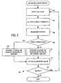
- an exemplary technique 200 for implementing sigma-delta capacitance sensing suitably includes the broad steps of applying a voltage to measurable capacitance 102 (step 202), allowing charge to transfer from measurable capacitance 102 to a passive network 109 that includes integrating capacitance 108 (step 204), and then adjusting the charge on the passive network (step 210) based on threshold value (step 206).
- step 202 applies a voltage to measurable capacitance 102
- a passive network 109 that includes integrating capacitance 108
- step 210 adjusting the charge on the passive network
- Charging step 202 suitably involves applying a known voltage to the measurable capacitance 102 using any appropriate technique.
- a charging voltage e.g. a low or high digital output, a power supply signal and/or the like
- a controller signal pin or other switch 106 is applied by activating a controller signal pin or other switch 106 as appropriate.
- a switch can be used to apply a voltage both by any combination of closing and opening depending upon the layout of the particular implementation.
- a charging voltage may be applied at least once to measurable capacitance 102 in one or more pulses (e.g. by repetitively engaging and disengaging switch 106), or through any other technique.
- measurable capacitance 102 is allowed to share charge with a passive network 109 capable of approximately integrating and storing charge without amplifiers or other active elements.
- the passive network 109 is simply integrating capacitance 108, which can be a single capacitor; alternatively, the passive network 109 may contain any number of resistors, capacitors and/or other passive elements as appropriate, and a number of examples of passive networks are described below.
- no action may be required other than to pause (e.g. while not charging the measurable capacitance) for a time sufficient to allow charge to transfer.
- the pause time may be relatively short (e.g.
- allowing charge to transfer may involve actively actuating one or more switches (e.g. switch 106 in FIG. 1 ) or taking other actions as appropriate.
- steps 202 and/or 204 can be repeated two or more times before taking further action.
- the measurable capacitance 102 may be statically coupled to the filter capacitance
- charge sharing between capacitances can be considered to substantially begin when the charging step 202 ends (e.g., when the applying of voltage to the measurable capacitance ends).
- the charge sharing between capacitances can be considered to substantially end when the voltages at the capacitances are similar enough that negligible charge is being shared.
- Charge sharing can also substantially end with the next application of a voltage because the (e.g. 104 charging) voltage being applied dominates.
- the low impedance of the applied voltage source makes the charge on the measurable capacitance that would be shared negligible until the applied voltage is removed.
- the charge on the passive network 109 is appropriately measured (step 206), and changed (step 210) if the amount of charge is determined to be past a suitable threshold value (step 208).
- Charge measurement may take place in any manner,
- the voltage on passive network 109 representative of that charge is obtained from an input/output (I/O) pin of a microcontroller or other device.
- circuitry associated with the input pin is also capable of performing an analog-to-digital (A/D) conversion or of comparing the.measured voltage to one or more threshold voltages V TH , thereby effectively performing both steps 206 and 208.
- the particular threshold value V TH (e.g.
- reference voltage 112 represented by the V cmp provided to quantizer 110 in FIG. 1
- V cmp may vary significantly by embodiment and may vary slowly with time.
- a CMOS digital input acts as a comparator (1-bit quantizer) with a reference voltage equal to the threshold level of the digital input.
- the connection of the quantizer 110 and the passive network can be direct or may be through a multiplexer or other switching network.
- the input has hysteresis, such as in a Schmitt trigger
- setting the hysteresis to a known state may be used to reliably select between thresholds on different comparisons. This may be accomplished by simply setting the input prior to the comparison to a value known to set the hysteresis state.
- a "delta" charge that opposes the charge shared from the measurable capacitance 102 is applied (e.g. via delta capacitance 126 in FIG. 1 ) to change the charge on the passive network 109 (step 210) using conventional sigma-delta techniques such as those described above.
- the charge on the passive network 109 may also be modified (albeit by a different amount than applied in step 208) when the charge has not passed the threshold value (step 211), although this feature is not necessary in all embodiments. Where there are multiple thresholds, different amounts of charge may be fed back. Note that in different states within a repetition of the steps of a charging cycle the charge transfer through various capacitances (e.g.
- measurable capacitance, delta capacitance, integrating capacitance may change direction, but the net charge transfer in the cycle is referred to here.
- the charge on passive network 109 can be maintained to what is needed for the associated voltage on passive network 109 to approximately equal the threshold value (V TH ), if the measurable capacitance 102 is within range. That is (with momentary reference again to FIG. 1 ) because the output of quantizer 110 is fed back via the delta capacitance 126 in a net negative feedback system, the voltage across the integrating capacitance 108 remains approximately constant during operation due to the control loop.
- the quantized (e.g. digital) values measured in step 206 and/or any quantity derived therefrom can be readily stored in a memory as quantized data and digitally filtered or otherwise processed as appropriate (step 212).
- Various filters have been successfully implemented in conjunction with sigma-delta measurement techniques, including conventional digital finite impulse response (FIR) filters such as triangle filters, averaging filters, and Kaiser filters, as well as infinite impulse response (IIR) filters.
- FIR digital finite impulse response
- IIR infinite impulse response
- the voltage application, charge transfer, charge changing and/or other steps may be individually and/or collectively repeated (step 214) any number of times to implement a number of useful features. For example, by obtaining multiple quantized values of measurable capacitance 102, the measured values can be readily decimated, filtered, averaged and/or otherwise digitally processed within the control circuitry to reduce the effects of noise, to provide increasingly reliable measurement values, and/or the like. A number of these features are described below.
- a versatile capacitance sensor can be readily implemented using only passive components in conjunction with a conventional digital controller such as a microcontroller, digital signal processor, microprocessor, programmable logic array, application specific integrated circuit and/or the like.
- a conventional digital controller such as a microcontroller, digital signal processor, microprocessor, programmable logic array, application specific integrated circuit and/or the like.
- a number of these products are readily available from various commercial sources including Microchip Technologies of Chandler, Arizona; Freescale Semiconductor of Austin, Texas; and Texas Instruments Inc. (TI) of Dallas, Texas.
- Many of the control circuits described herein contain digital memory (e.g. static, dynamic or flash random access memory) that can be used to store data and instructions used to execute the various sigma-delta processing routines described herein.
- Process 200 for example, may be readily implemented using computer-executable instructions executed by one or more control circuits as described herein.
- FIGS. 3-8 show several exemplary embodiments of sigma-delta capacitance sensors implemented using integrated control circuitry and simple passive networks made up of capacitors and/or resistors. Any of these embodiments may be supplemented or modified in myriad ways to create any number of alternate embodiments.
- an exemplary capacitance sensor 300 suitably includes a controller 302 with at least three input/output signal pins (I/Os) 304, 306 and 308 and their associated circuitry within controller 102 acting as switches to power and ground (or other reference values as appropriate).
- I/O 3 pin 308 is coupled to measurable capacitance 102
- the other two pins I/O 1 (pin 304) and I/O 2 (pin 306) are coupled to a passive network 109, comprising integrating capacitance 108, which is charged through measurable capacitance 102 and discharged through delta capacitance 126, or vice versa.
- Integrating capacitance 108 is generally selected to exhibit a much greater capacitance than that expected of measurable capacitance 102, and delta capacitance 126 is selected to set the maximum measurable capacitance.
- the particular capacitance values and relationships may vary according to the particular embodiment, as may the particular arrangement of the signal pins and passive network 109 components.
- FIG. 3B shows a "series" configuration of a three-pin, two-capacitor sensor 350 that operates in a manner similar to the "parallel" arrangement shown in FIG. 3A .
- controller 302 appropriately sequences and controls the sigma-delta measurement process by controlling signals placed and received on input/output (I/O) pins 304, 306, and 308.
- controller 302 suitably samples the charge on integrating capacitance 108 by measuring the voltage on pin 308.
- the voltage might be measured on other nodes.
- This voltage which corresponds to the input of quantizer 110 in FIG. 1 , can be quantified in many embodiments using a digital input threshold, an on-board ADC, or a Schmitt trigger input available within controller circuit 302.
- analog comparator circuitry for comparing the voltage on pin 308 to a suitable reference value 112 ( FIG.
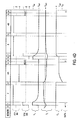
- FIGS. 3C-D An exemplary technique for operating the sensor circuit 300 of FIG. 3A is illustrated in FIGS. 3C-D .
- a substantially constant charging voltage e.g. from a battery, a power supply voltage such as V DD , or other reference voltage
- V DD voltage supply voltage
- Signal pin 306 is also driven to the same charging voltage to remove any charge held on delta capacitance 126.
- the charge applied to measurable capacitance 102 can then be isolated on measurable capacitance 102 by placing pins 306 and 308 into an intermediate high impedance or "open circuit” state, as indicated in "State 2".
- This intermediate state represents the non-overlapping switch states, although the technique could also be accomplished without an explicitly separate state. Other transitions might also be managed with other intervening high impedance states.
- the charge is subsequently shared from measurable capacitance 102 to passive network 109 by applying a logic state voltage on pin 304 that is opposite to the state of the charging voltage (e.g. by applying a "low” state if the charging voltage is "high”, and vice versa) in State 3.
- the voltage on integrating capacitance 108 (referenced to pin 304) should remain roughly constant and approximately equal to the threshold voltage of pin 308 (e.g. V TH of the associated I/O).
- the voltage at the signal pin 308 similarly remains relatively close to the threshold of input pin 308 when signal pin 304 is driven low.
- the output of the quantizer (signal pin 308), then, when sampled in State 4, is a measure of the charge on integrating capacitance 108.
- State 5 changes the charge on integrating capacitance 108.
- state 5A removes charge from the integrating capacitance 108; otherwise, no (or negligible) charge is removed (state 5B).
- signal pin 308 can be placed into a high-impedance state to trap charge on passive network 109 for a subsequent sampling on pin 308 (State 6).
- the data may be filtered, decimated or otherwise processed as appropriate to determine a value of the measurable capacitance 102.
- the quantizer e.g. signal pin 308 has hysteresis
- State 1 had set the input high, so the lower threshold of the hysteresis determines the output.
- integrating capacitance 108 is discharged through measurable capacitance 102 and charged through delta capacitance 126, the charge is changed when it falls below the quantizer threshold:
- positive or negative charges may be shared with integrating capacitance 108 though measurable capacitance 102 and delta capacitance 126, though no charge may be shared, and other nodes (e.g. pin 304 of FIG. 3A ) may be used for threshold measurement.
- FIGS. 4A-B show similar implementations that allow sigma-delta sampling with only two signal pins 304 and 306 on controller 302.
- the passive network 109 suitably includes an integrating capacitance 108 in series with an isolating resistor 402 coupled to the measurable capacitance 102 and to signal pin 306.
- the FIG. 4A implementation also includes a delta capacitance 126 coupled to signal pins 304 and 306.
- the FIG. 4A implementation (and others) can also optionally include a second capacitance 407 between a power supply voltage and the isolating resistor 402 to increase power supply noise rejection.
- the second capacitance 407 is selected so noise on the power supply couples to node 403 in the same ratio as noise on the power supply couples to the threshold(s) of the quantizer generically presented as 110 in FIG. 1A .
- FIGS. 9A-B show two topologies for reducing the effects of power supply noise, and two examples are shown in FIGS. 9A-B.
- Figure 9A shows a resistor 901 in parallel with the capacitance 407A and in series with capacitance 407B coupled to one or more integrating capacitances 108.
- FIG. 9B shows two resistors 903, 905 forming a voltage divider coupled to one or more integrating capacitances 108 and no discrete second capacitance.
- FIG. 4B "series" variation of 400 shows a passive network 109 comprising an isolating resistor 402 separating the measurable capacitance 102 from the integrating capacitance 108.
- measurable capacitance 102 is charged with charging pulses that are short enough to be substantially blocked by the RC time constant created by integrating capacitance 108 and isolating resistor 402.
- the charging pulse is preferably also shorter than the RC time constant of the measurable capacitance and the isolating resistor as well. This allows charging of measurable capacitance 102 and measurement of the voltage on integrating capacitance 108 to take place using the same pin.
- the voltage measured on either signal pin 304 or pin 306 can determine whether charge from delta capacitance 126 is to be shared with integrating capacitance 108. In the FIG.
- signal pin 306 is used to apply the charging voltage to measurable capacitance 102 and signal pin 304 is used to apply a charging voltage to delta capacitance 126.
- the FIG. 4B embodiment differs, and signal pin 306 is used to apply a charging voltage to delta capacitance 126 to change the charge on integrating capacitance 108, and signal pin 304 is used to apply the charging voltage to measurable capacitance 102. Note that in the FIG. 4B embodiment, it is simple to share charge from the measurable capacitance 102 to integrating capacitance 108 multiple times without sharing from the delta capacitance 126, or to share charge from the delta capacitance 126 to integrating capacitance 108 multiple times without sharing charge from the measurable capacitance 102.
- a "current canceling" voltage may precede the charging voltage.
- the timing of the "current canceling" voltage is controlled so the amount of "parasitic” charge removed through isolating resistor 402 in state 0 is mostly equal to the amount of "parasitic” charge added to integrating capacitance 108 through isolating resistor 402 in state 1, and the measurable capacitance 102 is left at the proper charging voltage before sharing with the passive network 109. This may allow for lower impedances in passive network 109, such as a lower value for isolating resistor 402, and faster time constants for passive network 109 as a whole without changing the measurable capacitance charge timing requirements.
- Measurable capacitance 102 shares charge with integrating capacitance 108 through isolating resistor 402. Because of the RC time delay created by the resistor, this embodiment may consume more time for sharing charge than the three-pin embodiment described with respect to FIG. 4 . Nevertheless, by reducing the number of switches/logic pins used to implement the sensor, additional sensing channels can be provided on a common chip, thereby allowing for improved efficiency in some embodiments.
- delta capacitance 126 may be replaced with a conventional resistor, and "delta" charge may be applied to integrating capacitance 108 by simply activating pin 304 (pin 306 in FIG. 4B ) for a pre-determined period of time.
- isolating resistor 402 may be useful in reducing the effects of any hysteresis present in the ADC feature of signal pin 306.
- the process of detecting the level of measurable capacitance 102 optionally begins by placing signal pin 306 into a known (e.g. logic low) state (State 0). Because isolating resistor 402 creates an RC time constant with integrating capacitance 108, pin 306 (pin 304 in FIG. 4B ) may be placed into a known state (e.g. a logic low state) prior to each read cycle for a brief period of time without significantly affecting the amount of charge stored on integrating capacitance 108.
- a known state e.g. a logic low state
- the measurable capacitance 102 is then charged and delta capacitance 126 is cleared by placing both pins 304 and 306 into a known (high) logic state, as shown in State 1.
- Charge is subsequently trapped on the measurable capacitance by bringing pin 306 to a high impedance state (State 2), and sufficient delay time is subsequently allowed for charge to share (e.g. charge or discharge) from measurable capacitance 102 to integrating capacitance 108 through isolating resistor 402.
- "delta" charge from delta capacitance 126 is applied or not applied based upon the voltage measured on integrating capacitance 108 (in the previous State 6).
- the voltage level used in determining whether "delta" charge is applied was obtained from a prior iteration of the sigma-delta process.
- voltage may be measured (e.g. State 3) just prior to application and sharing of "delta charge,” or at other points in the detection process.
- FIG. 5 Even further reductions in signal pin usage can be realized using the sensor 500 shown in FIG. 5 , in which measurable capacitance 102 and a passive network 109 composed of integrating capacitance 108 and isolating resistance 402 are coupled to a single signal pin 306 of controller 302. Similar to the FIG 4A implementation, the FIG 5A implementation can also optionally include a second capacitance 407 between a power supply voltage and the isolating resistance 402, or an alternative such as one of the circuits shown in FIGS. 9A-B to increase power supply noise rejection.
- measurable capacitance 102 is again charged with voltage pulses that have periods less than the RC time constant created by isolating resistance 402 and integrating capacitance 108 to reduce or eliminate adverse effects upon the charge stored on integrating capacitance 108.
- Measurable capacitance 102 discharges through isolating resistance 402, as described above, and "delta" charge is applied to integrating capacitance 108 by placing a discharging voltage on pin 306 to drive current through isolating resistance 402 for a known period of time.
- sensor 500 includes an isolating resistance 402 as described above, compensation for hysteresis on pin 306 can be similarly applied by placing the pin in a known state prior to sampling it. Parasitic currents through resistance 402 during states 0 and 1 can also be minimized by controlling the timing of the charging voltage, and the "current canceling" voltage.
- pin 306 is optionally set to provide a "current cancelling" voltage (e.g. ground) preceding the charging voltage; the length of the "current cancelling" voltage is chosen so the amount of parasitic charge removed is mostly equal to the amount of parasitic charge added by the charging pulse.
- a "current cancelling" voltage e.g. ground
- the length of the "current cancelling” voltage is chosen so the amount of parasitic charge removed is mostly equal to the amount of parasitic charge added by the charging pulse.
- the charge can be measured by sampling the voltage on pin 306 (State 3), and "delta" charge can be applied (or not applied) to integrating capacitance 108 as appropriate (State 4) based upon the measured voltage. Again, “delta” charge is simply applied in this embodiment by applying an appropriate voltage on signal pin 306 for an appropriate time to produce the desired change in charge on integrating capacitance 108.
- FIGS. 6A-B show two examples of circuits capable of sensing capacitance on multiple channels using the techniques shown above.
- an exemplary two-channel position sensor 600 is shown with two sensing electrodes 602, 604 that each correspond to a measurable capacitance 102 in the discussion above.
- the capacitances of that node change in a manner that can be correlated to the presence of the object.
- the presence of an object in proximity or in contact with either electrode 602, 604 can be determined by measuring the capacitance of that electrode channel.
- each channel (A and B) of sensor 600 generally parallels the two-pin sensor 400 described in conjunction with FIG. 4A above. Alternate embodiments could of course use any of the other techniques described or referenced herein.
- voltage is applied to electrodes 602 and 604 via pins 306 and 310, respectively, of controller 302. Each electrode 602, 604 is allowed to share charge with an integrating capacitance 108A, 108B through an isolating resistance 402A, 402B (respectively).
- Levels of charge maintained on each integrating capacitance 108A-B are then sampled by quantizing the voltage at signal pins 306 and 310, with any necessary "delta" charge from delta capacitance 126A-B being applied through manipulation of signal pins 304 and 308 to change the charge on the associated integrating capacitance.
- any integrating capacitances, delta capacitances, and/or resistances required can be shared between multiple sensor channels.
- FIG. 6B One exemplary embodiment is shown in FIG. 6B . This use of shared components can reduce the cost and size of the overall system significantly. Indeed, various techniques can be implemented for sharing signal pins on controller 302 and/or any discrete components within the passive network 109 across a wide array of alternate embodiments.
- sensing electrodes for measurable capacitances and other electrodes for delta capacitances can be readily formed on standard printed circuit boards (PCB), so duplication of these elements is relatively inexpensive in a manufacturing sense.
- PCB printed circuit boards
- Certain components such as integrating capacitance 108 and isolating resistance 402, however, can be large enough to warrant discrete components.
- the accuracy of the delta capacitance is a concern it may be implemented as a discrete component as well.
- one or more isolating resistances 402 may be formed on a PCB using an ink process or the like where conductive ink has higher resistance than typical materials used in PCB processes.
- Arranging the sensing electrodes 602, 604 in any number of conventional patterns allows for many diverse types of sensor layouts (including multi-dimensional layouts found in one, two or more-dimensional touchpad arrays) to be formulated.
- sensor layouts including multi-dimensional layouts found in one, two or more-dimensional touchpad arrays
- multiple "button"-type touch sensors can be readily formed from the various channels, or any number of other sensor layouts could be created.
- each sensor electrode 602, 604 can be easily implemented with common reference and logic voltages, it can be readily assumed that the typical voltage values observed on the various sensor electrodes 602, 604 will be roughly identical to each other averaged over time.
- a guard signal from a low impedance source to the various electrodes during otherwise inactive periods, then, the amount of spurious effect can be reduced, In fact, a single guard signal could be effective for all sensor electrodes with a similar sensing electrode voltage swing.
- a low impedance voltage source dominates other coupled signals at a node, just as the low impedance leg of a voltage divider (or more generically an impedance divider) dominates over the higher impedance leg. That is to say that for a collection of voltage sources we can be approximated as single Thevenin impedance and single Thevenin voltage dominated by the lowest impedance element, if that lowest impedance is substantially less that the parallel impedance of all other sources. For the purposes of this example the output impedance of a reference voltage, signal pin output, switch, or I/O output will have sufficiently low impedance at that node that other sources are insignificant at the range of frequencies considered.
- a node coupled to one near side of the integrating capacitance has sufficiently high capacitance (and low impedance) that it dominates other capacitively coupled sources, when the other far side of the integrating capacitance is driven with a low impedance (e.g. reference voltage etc.). That is the integrating capacitance can set the voltage at and absorb the majority of the charge from other higher impedance sources at the near end, when the far end is driven with a low impedance source.
- the dominant impedance in a network also depends on the time period (or frequency) considered. So at long time scales (e.g.
- a resistance in series with the integrating capacitance may not change the integrating capacitance's status as the dominant low impedance element, while at short time scales (e.g. charging) the impedance of the measurable capacitance on the node may dominate due to that series resistance.
- one technique involves applying a guarding voltage to the guarding electrode 605 that is approximately equal to the voltage applied to the active electrode (e.g. electrode 602 or 604) during the charging period.
- the voltage applied to the guarding electrode 605 is changed to be approximately equal to the voltage on the active sensor electrode and the associated integrating capacitance (The active sensor electrode and the associated integrating capacitance will typically approach the same voltage as charge sharing occurs).
- a threshold voltage of an associated quantizer e.g.
- an impedance divider may be used to reduce power supply variation sensitivity when the impedance divider output sensitivity is ratioed to the power supply similarly to the quantizer threshold sensitivity; an example of this impedance divider is shown by the voltage divider formed by resistances 606, 608 in FIG. 6A .
- the guard swing (and the charge transferred from the guard electrode) could change from one repetition of the charge transfer process to another (the charge transfer process includes the applying step, the allowing step, and the changing step).
- This guard voltage swing could average to the same voltage swing as on the sensing electrodes. If the change in guard swing involves having a guard swing of zero in some cases and a constant value in the other cases, this enables a pulse-code modulated guard technique that does not require any extra components. An offset between the guarding electrode voltage and the sensing electrode voltage would not affect the usefulness of the guard, since for charge transfer through a capacitance only the voltage change is important.
- sensor 600 utilizes an impedance divider that uses two resistances 606 and 608, that this is merely one example of the type of impedance divider that can be used.
- a typical impedance divider includes two passive impedances in series, with each passive impedance coupled to at least two nodes. One of those nodes is the common node to which both impedances couple. The common node provides the output of the impedance divider. The output of the impedance divider is a function of the voltages and/or currents applied at the "unshared nodes" over time.
- Simple examples of impedance dividers are voltage dividers that comprise two capacitances or two resistances (e.g., resistances 606 and 608).
- complex impedance dividers can also be used. These more complex impedance dividers can include unmatched capacitances, resistances, or inductances in series or in parallel. Furthermore, individual impedances can have a combination of capacitive, resistive and inductive characteristics.
- Guarding voltages may be applied using the features associated with signal pins 604 ( FIG. 6A ) or 310 ( FIG. 6B ) as appropriate.
- a voltage divider from the power supply (V DD ) is created using resistances 606 and 608, with pin 602 effectively switching resistance 608 in or out of the voltage divider circuit to create two separate voltages applied to guarding electrode 605.
- the embodiment shown in FIG. 6B similarly shows a divider circuit that includes a resistance 608 and a capacitor 614, with signal pin 310 controlling the guarding voltage applied to guarding electrode 605 to either the charging voltage or relaxing to a threshold voltage (acting much like how circuit 500 shown in FIG. 5A does when it shares charge).
- the impedance driving the guarding voltage should be less than the total sensor-coupled-impedance to the guarding electrode for the most effective guarding.
- a variety of other guarding techniques including active analog components such as buffers or operational amplifiers (OP-AMPS) that track a sensor or reference channel may also be used.
- FIGS. 6A-B are generally based upon the embodiments described in conjunction with FIG. 4A-D above, guarding concepts may be applied across a wide array of capacitance sensors. Nevertheless, guarding is an optional feature that may not be found on all embodiments.
- the sensor 650 shown in FIG. 6B shows a simple technique whereby delta capacitance 126 and integrating capacitance 108 are shared between two sensing electrodes 602 and 604.
- the sensor 700 shown in FIG.7A similarly shows a simple technique by which a signal pin 308 for applying delta capacitance 126 can be shared between two sensing channels (represented by measurable capacitances 102A-B).
- sensor 700 is operated in a manner similar to sensor 350 described above in conjunction with FIG. 3B , but with charge feedback to the sides of delta capacitances 126A-B provided through a common signal pin 308.
- this embodiment changes phases to determine whether or not a particular integrating capacitance (e.g., 108A or 108B) is sensitive to a transition on the corresponding delta capacitance (126A and 126B).
- each integrating capacitance can selectively share charge or block charge transfer from the measurable capacitance or the delta capacitance depending upon which side of the integrating capacitance is driven at a low impedance.
- each delta capacitance can be allowed to transition without affecting the measurable capacitance, and the signal pin 308 can be shared with multiple sensors reducing pin count.
- a driven sensing electrode e.g. 802 in FIG. 8A
- These concepts can be similarly applied to any number of additional sensing channels to further improve component and/or signal pin re-use between multiple measurable capacitances 102.
- FIG. 7B includes a state diagram 750 that illustrates an exemplary state sequence for sensor 700.
- the first state 1 is to discharge the measurable capacitances by setting pins 304 and 312 to 0, while measuring (quantizing) the voltage at the integrating capacitances using I/Os associated with pins 306 and 310.
- the transitions in the state diagram for pins 304 and 306 indicates that the voltage at pin 306 measured (quantized data 1) high during state 1
- the transitions in the state diagram for pins 310 and 312 indicate that 310 measured (quantized data 0) low during state 1.
- the second state 2 comprises an intermediate high impedance state.
- the signal pins 3 04, 3 06, 310 and 312 are all briefly held in a high impedance state, with pin 308 driving the delta capacitances 126A-B low.
- the third state 3 puts the electrode of integrating capacitances 108A and 108B coupled to the delta capacitances 126A-B at a logic high voltage. This causes the voltage on the measurable capacitances 102A-B to change and to share charge with their respective integrating capacitances 108A-B. At the same time by driving the signal pins 306 and 308 to a low impedance charge transfer coupled through the delta capacitances 126A-B is blocked.
- the fourth state 4 clears the charge on delta capacitances 126A and 126B since both sides of these capacitors are set to the same logic high voltage by pins 306, 308, and 310.
- the fifth state 5 puts pin 306 at a high impedance state, which holds the charge on integrating capacitance 108A.
- This is an intermediate high impedance state on signal pin 304 for measurable capacitance 102A before it transitions in the following state 5 and prevents charge from inadvertently being set on the integrating capacitance 108A.
- the pin 310 coupled to integrating capacitance 108B which had a voltage at pin 310 with a quantized data measurement of 0 remains driven to a logic high voltage, because that integrating capacitance did not require charge modification by delta capacitance 126B.
- the sixth state 6 drives the signal pin 304 to a low logic level so that a delta charge can be transferred through delta capacitance 126A to integrating capacitance 108A in the subsequent step 7.
- pin 310 remains driven to a logic high level blocking this delta capacitance charge transfer between 126B and 108B.
- this low logic level transition on pin 304 also causes the charge to share from parasitic capacitances and delta capacitances in this step rather than in future step I as already described.
- the seventh state 7 transitions the voltage on pin 308 to remove charge through the delta capacitance 126A from the integrating capacitance 108A, while the charge on integrating capacitance 108B is not substantially affected.
- the final state 8 comprises a second intermediate high impedance state for integrating capacitances (e.g. 108B) that did not require charge modification in step 7, and to prepare them for sharing in the following steps. This again decouples the various capacitors to temporarily trap charge in those capacitors.
- capacitances e.g. 108B
- step 8 the method returns to step I and the states 1-8 are executed again. It should be noted that this sequence produces results from the measurements at pins 306 and 308 of a voltage on the integrating capacitances 108A-B and quantized data (e.g. 0 or 1) suitable for a determination of their respective measurable capacitances 102A.
- sequence of steps for measurable capacitance 102A and pins 304 and 306, as well as, measurable capacitance 102B and pins 310 and 312 are exemplary only of a particular measurement (and quantization) of the voltage on pins 306 and 310 in the exemplary step 1, and either sequence of states could be present on either measurable capacitance and integrating capacitance depending on that measurement in a repetition of the measurement cycle.
- sequences of states will occur on the related pins, and resulting quantized data (e.g. 0 and 1) of both types will be part of any result used to determine the measurable capacitance.
- this embodiment facilitates several advantages. For example, because the common node (i.e., pin 308) is always driven, the of effect of parasitic capacitance may be significantly reduced. Second, sensor 700 may reduce the number of cycles that it takes to apply the IO states and sample multiple capacitances since it allows sampling (i.e. quantizing at multiple I/Os simultaneous) in parallel. Finally, it will allow significantly fewer IOs when many measurable capacitances are detected. This embodiment can also reduce the sensitivity to external noise coupled by the measurable capacitances or other associated parasitic capacitances coupled to pins 304 and 312 by grounding the nodes coupled to the measurable capacitances (i.e. pins 304 and 312) during integrating capacitance charge measurements.
- FIG. 8A shows another embodiment of a sensor 800 that is designed to work with so-called “driven capacitance” or “transcapacitive” sensors.
- the sensor 800 is a "series” sensor as the integrating capacitance 108 is in series with the delta capacitance 126 and the measurable capacitance 102.
- the measurable capacitance 102 is formed by two separate electrodes 802, 804, each of which may be driven to a voltage using signal pins 304, 306 of controller 302.
- FIG. 8B includes a state diagram 825 that illustrates an exemplary state sequence for sensor 800.
- a delta charge may be added to the integrating capacitance 108 through delta capacitance 126 (Cd) by changing the state of I/O4 on signal pin 310.
- This change of logic state on 310 from low to high logic levels (or just staying low) in state 1 is depends as a function of F(V CI ) on a previous quantization of the voltage on integrating capacitance 108 at pin 308 in a previous state 7.
- the function F(V CI ) if voltage at the integrating capacitance 108 was higher than the threshold voltage V TH for I/O3 of signal pin 308 in the previous cycle (i.e., the charge on the integrating capacitance is low, and the voltage drop smaller than desired), then pin 310 remains low. If instead, the voltage at the integrating capacitance 108 was lower than the threshold voltage (i.e., the charge on the integrating capacitance is high, and the voltage drop larger than desired), then pin 310 is driven high to raise the voltage at 308 by removing charge from integrating capacitance 108 through delta capacitance 126.
- charge is also transferred through measurable capacitance Cx 102 between electrodes 802 and 804 as I/O1 transitions from low to high adding charge to the integrating capacitance.
- measurable capacitance Cx 102 By adding charge through the measurable capacitance 102 and removing charge through the delta capacitance 126 under the control of the sigma-delta system the charge on the integrating capacitance 108 is kept roughly constant by negative feedback control.
- state 1 either does (i.e. la) or does not (i.e. 1b) remove charge from integrating capacitance 108 using delta capacitance 126 based on the previous voltage measurement at I/O3 of the integrating capacitance on pin 308.
- This measurement might be done in a variety of ways in alternate embodiments, for example the measurement of voltage on the integrating capacitance might use pin 306.
- State 2 is an intermediate high impedance state on both sides of integrating capacitance 108 (ie. signal pins 306 and 308). This traps the integrated charge on integrating capacitance 108 so that any timing errors on the outputs of the signal pins to not change the charge on it.
- Pin 304 remains driven low, and pin 310 is left in its previous state.
- the signal pin 308 is set to a low logic state (e.g. ground). Note that the voltage on pin 308 was measured in the previous state 7, and should have been close to a threshold of an input associated with signal pin 308 and I/O3.
- a logic low state By driving 308 to a logic low state and changing the voltage on one side of integrating capacitance 108 the voltage at sensing electrode 804 also changes and the integrating capacitance 108 shares charge with the measurable capacitance 102, as well as with any other parasitic capacitance coupled to the node at signal pin 306 and sensor 804.
- the charge shared with the measurable capacitance 102 is in the same direction as the charge transferred by driving I/O1 on pin 304 high in the following step, though this need not be the case in all implementations.
- the charge shared onto the integrating capacitance 108 from the parasitic capacitance due to any voltage change on 804 occurs just as in other "absolute capacitance" sensors described elsewhere in this docunient, though this example is meant to function as a transcapacitive sensor.
- This parasitic charge is shared onto integrating capacitance 108, and in this example will tend to add charge to it, reducing the measured voltage on integrating capacitance 108 at pin 3 08.
- the fifth state 5 is another high impedance state decoupling both sides of the integrating capacitance 108.
- Driving a low impedance on the signal pin 306 of I/O2 shields the integrating capacitance 108 from any noise coupled to that electrode during the following measurement step. It also allows charge to share through the integrating capacitance 108 with the node connected to signal pin 308 and delta capacitance 126.
- the voltage at the 308 signal pin node is also changed. This again causes charge to be shared through any parasitic capacitance on pin 308 with the integrating capacitance 108.
- the seventh state 7 measures the voltage on the integrating capacitance 108.
- the voltage (due to the integrated charge) on the integrating capacitance 108 can be measured at pin 308 relative to the voltage driven on the sensing electrode by signal pin 306.
- This measurement can comprise a comparison of the voltage at the integrating capacitance 108 with a threshold voltage V TH to provide a quantized result.
- the resulting measurement of the voltage on integrating capacitance 108 i.e. whether it is higher than threshold voltage V TH
- the repeated execution of states 1-7 will result in sigma-delta closed loop control of charge on the integrating capacitance 108, and a filtered measurement of the quantized results can be used to measure the transcapacitance between electrodes 802 and 804.
- This measured transcapacitance can further be used to sense the proximity of an object relative to the sensor or for any other purpose.
- the transcapacitive sensor 850 is a parallel sensor, in that the measurable capacitance 102 is in parallel with the delta capacitance 126 in its connection to integrating capacitance 108. Also, in this embodiment a voltage V G close to threshold voltage V TH is generated with a voltage divider comprising resistances 812 and 814. As with the previous embodiment, the measurable capacitance 102 is formed by two separate electrodes 802, and 804, each of which may be driven to a voltage using signal pins 304, 306 of controller 302.
- capacitive coupling (indicated by the measurable capacitance 102) between electrodes 802 and 804 can be detected using sigma-delta sensing techniques to sense the charge transferred between the electrodes 802, 804 and to the passive network 109 comprising integrating capacitance 108.
- FIG. 8D includes a state diagram 875 that illustrates an exemplary state sequence for sensor 850.
- the first state 1 comprises an intermediate high impedance state.
- the signal pins 306, 308A and 308B are all held in a high impedance state, with pin 304 driven to a logic low voltage, and pin 310 driven to a logic high voltage.
- the voltage on the integrating capacitance 108 at node 851 is set to a generated voltage V G implemented to substantially equal the threshold voltage V TH of the measuring I/O (e.g. IO3).
- pin 308A provides a logic high voltage (e.g. V DD )
- pin 308B provides a logic low voltage (e.g. GND)
- resistances 812 and 814 provide a voltage divider that generates a voltage V G at node 851.
- the resistances 812 and 814 are substantially equal, and the generated voltage is thus proximately 1 ⁇ 2 V DD , comparable to a CMOS input threshold.
- passive components and switches e.g.
- the threshold voltage of a digital input is the voltage that distinguishes a low from a high input.
- Vdd/3 might approximate the input threshold of the I/O3 which was just set to a logic high.
- the voltage divider will not be used. Instead, in some embodiments the controller 302 inherently includes the ability to generate an appropriate voltage V G near V TH .
- driving node 851 with a generated voltage Vg near the threshold voltage V TH reduces the voltage swing on electrode 804 in steps 2-3, because the sigma-delta feedback loop controls the charge on the integrating capacitance 108 to keep the voltage on the node 851 near the threshold voltage when signal pin 306 drives node 804 (in steps 5,6,7) and an input connected to node 851 (e.g. 308A) can be measured.
- Keeping the voltages at 804 and 851 constant makes parasitic capacitance to fixed voltages (e.g. GND) largely irrelevant since no charge moving through the parasitic capacitance is minimized. Note that if measurements of the voltage on integrating capacitance 108 were done with I/O2 on pin 306 then the node 306 might be driven with a similar generated voltage Vg to minimize the effect of parasitic capacitance.
- a delta charge is transferred to the integrating capacitance 108 and/or charge is shared between the electrode 804 and the integrating capacitance 108, depending on previous measurements of the voltage on the integrating capacitance 108 at 308A.
- the pin 310 is driven as a function of F(V CI ) of the previously measured voltage on the integrating capacitance 108 at 308A.
- the function F(V CI ) is selected such that if voltage at the integrating capacitance 108 (e.g., at node 851) was higher than the threshold voltage V TH for I/O3 in the previous repetition of the measurement cycle _ (i.e., the charge on the integrating capacitance is low, and the voltage drop smaller than desired), then pin 310 is remains at a logic high voltage. If instead, the voltage at the integrating capacitance 108 was lower than the threshold voltage (i.e., the charge on the integrating capacitance is high, and the voltage drop larger than desired), then pin 310 is driven to a logic low voltage to remove charge from integrating capacitance 108 through delta capacitance 126.
- charge is also transferred through measurable capacitance Cx 102 between electrodes 802 and 804 as I/O1 transitions from a logic low voltage to a logic high voltage adding charge to the integrating capacitance.
- measurable capacitance Cx 102 By adding charge through the measurable capacitance and removing charge through the delta capacitance under the control of the sigma-delta system the charge on the integrating capacitance is kept roughly constant by negative feedback control.
- state 3 either shares charge between electrode 804 and integrating capacitance 108 or removes charge from integrating capacitance 108 using delta capacitance 126 based on the previous voltage measurement at I/O3 on pin 308A of the integrating capacitance.
- the fourth state 4 comprises another intermediate high impedance state that assures that there is no signals that could otherwise inadvertently set an unwanted charge on a capacitor.
- the fifth state 5 sets the receiving electrode 804 to a logic high voltage again through I/O2 on signal pin 306.
- the sixth state 6 sets the charges on the measurable capacitance (C X ) 102 and the delta capacitance (C D ) 126 in preparation for transitions on a following repetition of the charge transfer process. Specifically, a logic high voltage is put on pin 310 while a logic high voltage is also put on pin 306 discharging delta capacitance 126. At the same time a logic low voltage is placed on electrode 802 through signal pin 304 recharging the measurable capacitance coupled to electrode 804.
- the seventh state 7 measures the voltage at the integrating capacitance 108.
- the voltage (due to the integrated charge) on the integrating capacitance 108 e.g., the voltage at node 851
- This measurement can comprise a comparison of the voltage at the integrating capacitance 108 with the threshold voltage V TH to provide a quantized result.
- the resulting measurement of the voltage on integrating capacitance 108 i.e. whether it is higher than threshold voltage V TH ) will then be used in F(V CI ) in the next cycle during states 3-5 determining how the charge on integrating capacitance might be changed by the delta capacitance 126.
- the repeated execution of states 1-7 will result in sigma-delta closed loop control of charge on the integrating capacitance 108, and a filtered measurement of the quantized results can be used to measure the transcapacitance between electrodes 802 and 804. This measured transcapacitance can further be used to sense the proximity of an object relative to the sensor
- the sensor embodiments illustrated in FIG. 8 measure transcapacitance rather than absolute or ground referenced capacitance. These embodiments reduce the negative effects of background or parasitic capacitance on the measured capacitance and thus are particularly usefully in applications where there is a higher proportion of parasitic trace capacitance, such as fingerprint ridge sensing and capacitive touch sensing.
- the amount of voltage swing on the sensed electrode 804 can be held to a relatively low level by sigma-delta feedback control. This can substantially reduce sensitivity to parasitic capacitance. That is, since the voltage on integrating capacitance 108 at node 851 remains relatively close to the threshold voltage during steady-state operation, both when the voltage is driven on node 851 (and 306 is floating), and when voltage is driven on 306, and node 851 is not driven by signal pins 308A/B.
- the voltage swing on electrode 804 is kept relatively low since signal pin 306 is driven to a voltage similar to what results when the voltage at node 851 is driven to a voltage at one of 308A/B's input thresholds (instead of driving signal pin 306 to some other voltage).
- the voltage difference between 851 and 306 is determined by the voltage across (and charge on) the integrating capacitance, which is controlled by the sigma-delta negative feedback loop.
- These voltages on 306 and node 851 can be applied in any manner.
- the approximate threshold voltage is applied using logic from pin(s) 308A-B to activate or deactivate a portion of a voltage divider network that results in the appropriate voltage.
- the approximate voltage may be applied by digital-to-analog converter, or by any other technique
- noise dither techniques can be reduced through the use of noise dither techniques.
- conventional first-order sigma-delta converters are known to be especially susceptible to noise "tones" (i.e. repeating patterns of noise). These tones can produce a noisy output for certain constant inputs (such that "dead zones” where capacitance sensitivity is low (or alternately, error is high) exist), resulting in reduced response to slight changes in input conditions.
- Tones can be avoided through the use of more sophisticated (i.e. higher order) sigma-delta techniques, or alternatively by injecting a small amount of low power noise into the sigma-delta converter.
- One technique for injecting noise involves applying a noise dither to the ADC reference voltage (e.g. voltage 112 in FIG. 1 ). This dither may be generated in any sort of software or other logic, and can be applied simultaneously to each of the sensing channels to improve response.
- FIG. 10 a block diagram is illustrated of an exemplary electronic system 10 that is coupled to a proximity sensor device 11.
- Electronic system 10 is meant to represent any type of personal computer, portable computer, workstation, personal digital assistant, video game player, communication device (including wireless phones and messaging devices), media device, including recorders and players (including televisions, cable boxes, music players, and video players) or other device capable of accepting input from a user and of processing information.
- the various embodiments of system 10 may include any type of processor, memory or display.
- the elements of system 10 may communicate via a bus, network or other wired or wireless interconnection.
- the proximity sensor device 11 can be connected to the system 10 through any type of interface or connection, including I2C, SPI, PS/2, Universal Serial Bus (USB), Bluetooth, RF, IRDA, or any other type of wired or wireless connection to list several non-limiting examples.
- Proximity sensor device 11 includes a controller 19 and a sensing region 18.
- Proximity sensor device 11 is sensitive to the position of an input 14 (which can be provided by one or more fingers, styli, and/or other input objects) in the sensing region 18, and can detect the input 14 by measuring the resulting changes in capacitance due to input 14.
- "Sensing region” 18 as used herein is intended to broadly encompass any space above, around, in and/or near the proximity sensor device 11 wherein the sensor is able to detect a position of the object. In a conventional embodiment, sensing region 18 extends from a surface of the sensor in one or more directions for a distance into space until signal-to-noise ratios prevent input detection.
- This distance may be on the order of less than a millimeter, millimeters, centimeters, or more, and may vary significantly with the sensor electrode dimensions, sensor design, and/or the sensor performance (e.g. accuracy or resolution) desired. Accordingly, the planarity and curvature, size, shape and exact locations of the particular sensing regions 18 will vary widely from embodiment to embodiment.
- proximity sensor device 11 suitably detects a position of input 14 by measuring the measurable capacitance(s) associated with the plurality of sensing electrodes which are affected by one or more fingers, styli, and/or other objects within sensing region 18. And, using controller 19, proximity sensor device 11 provides electrical or electronic indicia of the position to the electronic system 10. The system 10 appropriately processes the indicia to accept inputs from the user for any appropriate purpose and produces any appropriate responses, as discussed earlier.
- the proximity sensor device 11 can use discrete arrays, or any other arrangement of capacitive sensor electrodes to support any number of sensing regions 18.
- the proximity sensor device can also vary in the type of information provided, such as to provide "one-dimensional" position information (e.g. along a sensing region) as a scalar, "two-dimensional" position information (e.g. horizontal/vertical axes, angular/radial, or any other axes that span the two dimensions) as a combination of values, a "two-dimensional" image of the proximity as an array of values, and the like.
- controller 19 also communicates with the electronic system 10.
- the controller 19 can perform a variety of additional processes to implement the proximity sensor device 11. For example, the controller 19 can select or connect individual measurable capacitances, calculate position or motion information based on the values of the measurable capacitances, report a position or motion when a threshold is reached, interpret and wait for a valid tap/stroke/character/button/gesture sequence before reporting it to the electronic system 10 or indicating it to the user, or any of a multitude of different processes.
- controller is defined to include one or more processing elements that are adapted to perform the recited operations.
- the controller 19 can comprise all or part of one or more integrated circuits, firmware code, and/or software code.
- the term “electronic system” broadly refers to any type of device that communicates with proximity sensor device 11.
- the electronic system 10 could thus comprise any type of device or devices in which a touch sensor device can be implemented in or coupled to.
- the proximity sensor device 11 could be implemented as part of the electronic system 10, or coupled to the electronic system 10 using any suitable technique.
- the electronic system 10 could thus comprise any type of computing device, media player, communication device, or another input device (such as another touch sensor device or keypad). In some cases the electronic system 10 is itself a peripheral to a larger system.
- the electronic system 10 could be a data input or output device, such as a remote control or display device, that communicates with a computer or media system (e.g., remote control for television) using a suitable wired or wireless technique.
- a computer or media system e.g., remote control for television
- the various elements (processor, memory, etc.) of the electronic system 10 could be implemented as part of an overall system, as part of the touch sensor device, or as a combination thereof.
- the electronic system 10 could be a host or a slave to the proximity sensor device 11.
- proximity sensor device is intended to encompass not only conventional proximity sensor devices, but also a broad range of equivalent devices that are capable of detecting the position of a one or more fingers, pointers, styli and/or other objects. Such devices may include, without limitation, touch screens, touch pads, touch tablets, biometric authentication devices, handwriting or character recognition devices, and the like.
- position or “object position” as used herein are intended to broadly encompass absolute and relative positional information, and also other types of spatial-domain information such as velocity, acceleration, and the like, including measurement of motion in one or more directions.
- Various forms of positional information may also include time history components, as in the case of gesture recognition and the like. Accordingly, proximity sensor devices can appropriately detect more than the mere presence or absence of an object and may encompass a broad range of equivalents.
- the mechanisms of the present invention are capable of being distributed as a program product in a variety of forms.
- the mechanisms of the present invention can be implemented and distributed as a proximity sensor program on a computer-readable signal bearing media.
- the embodiments of the present invention apply equally regardless of the particular type of signal bearing media used to carry out the distribution.
- Examples of signal bearing media include: recordable media such as memory cards, optical and magnetic disks, hard drives, and transmission media such as digital and analog communication links.
Applications Claiming Priority (7)
| Application Number | Priority Date | Filing Date | Title |
|---|---|---|---|
| US68703905P | 2005-06-03 | 2005-06-03 | |
| US68714805P | 2005-06-03 | 2005-06-03 | |
| US68716605P | 2005-06-03 | 2005-06-03 | |
| US68716705P | 2005-06-03 | 2005-06-03 | |
| US68703705P | 2005-06-03 | 2005-06-03 | |
| US77484306P | 2006-02-16 | 2006-02-16 | |
| EP06760654A EP1894025A1 (fr) | 2005-06-03 | 2006-06-02 | Methodes et systemes de detection d'une capacitance utilisant des techniques de mesure sigma-delta |
Related Parent Applications (1)
| Application Number | Title | Priority Date | Filing Date |
|---|---|---|---|
| EP06760654.1 Division | 2006-06-02 |
Publications (1)
| Publication Number | Publication Date |
|---|---|
| EP2280483A1 true EP2280483A1 (fr) | 2011-02-02 |
Family
ID=36950514
Family Applications (2)
| Application Number | Title | Priority Date | Filing Date |
|---|---|---|---|
| EP10181010A Withdrawn EP2280483A1 (fr) | 2005-06-03 | 2006-06-02 | Procedes et systemes pour le blindage d'un capteur a capacite de transfert de charge pour la detection de proximite |
| EP06760654A Withdrawn EP1894025A1 (fr) | 2005-06-03 | 2006-06-02 | Methodes et systemes de detection d'une capacitance utilisant des techniques de mesure sigma-delta |
Family Applications After (1)
| Application Number | Title | Priority Date | Filing Date |
|---|---|---|---|
| EP06760654A Withdrawn EP1894025A1 (fr) | 2005-06-03 | 2006-06-02 | Methodes et systemes de detection d'une capacitance utilisant des techniques de mesure sigma-delta |
Country Status (2)
| Country | Link |
|---|---|
| EP (2) | EP2280483A1 (fr) |
| WO (1) | WO2006132960A1 (fr) |
Cited By (1)
| Publication number | Priority date | Publication date | Assignee | Title |
|---|---|---|---|---|
| WO2015050700A1 (fr) * | 2013-10-02 | 2015-04-09 | Synaptics Incorporated | Configuration de circuit d'attaque de dispositif d'affichage à écran tactile intégré multi-capteur pour dispositifs de détection capacitive |
Families Citing this family (20)
| Publication number | Priority date | Publication date | Assignee | Title |
|---|---|---|---|---|
| KR101063537B1 (ko) * | 2009-02-23 | 2011-09-07 | 주식회사 애트랩 | 커패시턴스 측정 회로 |
| US8049732B2 (en) | 2007-01-03 | 2011-11-01 | Apple Inc. | Front-end signal compensation |
| US8711129B2 (en) | 2007-01-03 | 2014-04-29 | Apple Inc. | Minimizing mismatch during compensation |
| DE102007007551A1 (de) * | 2007-02-15 | 2008-08-21 | Sick Ag | Induktiver Näherungssensor |
| TW200907313A (en) * | 2007-04-11 | 2009-02-16 | Silverbrook Res Pty Co Ltd | Capacitive force sensor having saturated output at minimum capacitance |
| AU2008238595B2 (en) * | 2007-04-11 | 2011-08-18 | Silverbrook Research Pty Ltd | Sensing device having capacitive force sensor |
| JP5239328B2 (ja) * | 2007-12-21 | 2013-07-17 | ソニー株式会社 | 情報処理装置及びタッチ動作認識方法 |
| FR2928458B1 (fr) * | 2008-03-06 | 2010-12-10 | Continental Automotive France | Dispositif de mesure d'une variation de capacite, capteur capacitif mettant en oeuvre un tel dispositif et procede associe |
| FR2938344B1 (fr) * | 2008-11-07 | 2010-11-19 | Continental Automotive France | Dispositif de mesure d'une variation de la capacitance d'une structure capacitive variable |
| CH700376A2 (de) | 2009-02-11 | 2010-08-13 | Baumer Innotec Ag | Kapazitiver Sensor und Verfahren zur kapazitiven Erfassung eines Objektabstandes. |
| CN105258714B (zh) | 2009-05-13 | 2018-10-19 | 辛纳普蒂克斯公司 | 电容传感器装置 |
| DE102011006079B4 (de) * | 2011-03-24 | 2012-12-06 | Ident Technology Ag | Messeinrichtung und Verfahren zur Annäherungsdetektion |
| KR102045784B1 (ko) * | 2012-04-04 | 2019-11-18 | 페어차일드 세미컨덕터 코포레이션 | 병합된 미세 전자기계 가속도계 센서에 대한 초핑을 이용하는 노이즈 감소 방법 |
| US9587964B2 (en) * | 2013-06-12 | 2017-03-07 | Microchip Technology Incorporated | Capacitive proximity detection using delta-sigma conversion |
| US9658722B2 (en) | 2013-09-26 | 2017-05-23 | Synaptics Incorporated | Using a printed circuit to offset charge during capacitive sensing |
| US10162038B2 (en) * | 2014-07-09 | 2018-12-25 | Stmicroelectronics S.R.L. | Method of interfacing a LC sensor and related system |
| CN106877854B (zh) * | 2017-02-09 | 2020-07-21 | 广东美的厨房电器制造有限公司 | 触摸按键的检测方法、检测装置及电器设备 |
| CN108008203B (zh) * | 2017-11-27 | 2020-12-08 | 合肥鑫晟光电科技有限公司 | 一种检测电路及电压补偿方法 |
| WO2021101916A1 (fr) * | 2019-11-18 | 2021-05-27 | Analog Devices, Inc. | Système de capteur d'impédance basé sur un pont |
| DE102021117002A1 (de) * | 2021-07-01 | 2023-01-05 | Valeo Schalter Und Sensoren Gmbh | Eingabevorrichtung für ein Kraftfahrzeug mit einer kapazitiven Sensorvorrichtung und Verfahren zur Erkennung der Betätigung einer Sensorelektrode einer entsprechenden Eingabevorrichtung |
Citations (2)
| Publication number | Priority date | Publication date | Assignee | Title |
|---|---|---|---|---|
| US5880411A (en) | 1992-06-08 | 1999-03-09 | Synaptics, Incorporated | Object position detector with edge motion feature and gesture recognition |
| EP1521090A2 (fr) * | 2003-09-30 | 2005-04-06 | Aisin Seiki Kabushiki Kaisha | Dispositif de détection de capacitance |
-
2006
- 2006-06-02 EP EP10181010A patent/EP2280483A1/fr not_active Withdrawn
- 2006-06-02 WO PCT/US2006/021437 patent/WO2006132960A1/fr active Application Filing
- 2006-06-02 EP EP06760654A patent/EP1894025A1/fr not_active Withdrawn
Patent Citations (2)
| Publication number | Priority date | Publication date | Assignee | Title |
|---|---|---|---|---|
| US5880411A (en) | 1992-06-08 | 1999-03-09 | Synaptics, Incorporated | Object position detector with edge motion feature and gesture recognition |
| EP1521090A2 (fr) * | 2003-09-30 | 2005-04-06 | Aisin Seiki Kabushiki Kaisha | Dispositif de détection de capacitance |
Cited By (9)
| Publication number | Priority date | Publication date | Assignee | Title |
|---|---|---|---|---|
| WO2015050700A1 (fr) * | 2013-10-02 | 2015-04-09 | Synaptics Incorporated | Configuration de circuit d'attaque de dispositif d'affichage à écran tactile intégré multi-capteur pour dispositifs de détection capacitive |
| US9298299B2 (en) | 2013-10-02 | 2016-03-29 | Synaptics Incorporated | Multi-sensor touch integrated display driver configuration for capacitive sensing devices |
| KR20160064212A (ko) * | 2013-10-02 | 2016-06-07 | 시냅틱스 인코포레이티드 | 용량성 센싱 디바이스들에 대한 멀티-센서 터치 통합 디스플레이 드라이버 구성 |
| JP2016535882A (ja) * | 2013-10-02 | 2016-11-17 | シナプティクス インコーポレイテッド | 静電容量感知デバイスのための多重センサタッチ統合表示ドライバ構成 |
| US9791990B2 (en) | 2013-10-02 | 2017-10-17 | Synaptics Incorporated | Multi-sensor touch integrated display driver configuration for capacitive sensing devices |
| US10067626B2 (en) | 2013-10-02 | 2018-09-04 | Synaptics Incorporated | Multi-sensor touch integrated display driver configuration for capacitive sensing devices |
| KR20200103123A (ko) * | 2013-10-02 | 2020-09-01 | 시냅틱스 인코포레이티드 | 용량성 센싱 디바이스들에 대한 멀티-센서 터치 통합 디스플레이 드라이버 구성 |
| KR102151837B1 (ko) | 2013-10-02 | 2020-09-04 | 시냅틱스 인코포레이티드 | 용량성 센싱 디바이스들에 대한 멀티-센서 터치 통합 디스플레이 드라이버 구성 |
| KR102411470B1 (ko) | 2013-10-02 | 2022-06-22 | 시냅틱스 인코포레이티드 | 용량성 센싱 디바이스들에 대한 멀티-센서 터치 통합 디스플레이 드라이버 구성 |
Also Published As
| Publication number | Publication date |
|---|---|
| EP1894025A1 (fr) | 2008-03-05 |
| WO2006132960B1 (fr) | 2007-02-01 |
| WO2006132960A1 (fr) | 2006-12-14 |
Similar Documents
| Publication | Publication Date | Title |
|---|---|---|
| US7683641B2 (en) | Methods and systems for detecting a capacitance using sigma-delta measurement techniques | |
| US7288946B2 (en) | Methods and systems for detecting a capacitance using sigma-delta measurement techniques | |
| EP2280483A1 (fr) | Procedes et systemes pour le blindage d'un capteur a capacite de transfert de charge pour la detection de proximite | |
| KR101340860B1 (ko) | 시그마 델타 측정 기술들을 사용하여 캐패시턴스를검출하기 위한 방법들 및 시스템 | |
| US7777501B2 (en) | Methods and systems for sigma delta capacitance measuring using shared component | |
| US7902842B2 (en) | Methods and systems for switched charge transfer capacitance measuring using shared components | |
| US7449895B2 (en) | Methods and systems for detecting a capacitance using switched charge transfer techniques |
Legal Events
| Date | Code | Title | Description |
|---|---|---|---|
| PUAI | Public reference made under article 153(3) epc to a published international application that has entered the european phase |
Free format text: ORIGINAL CODE: 0009012 |
|
| AC | Divisional application: reference to earlier application |
Ref document number: 1894025 Country of ref document: EP Kind code of ref document: P |
|
| AK | Designated contracting states |
Kind code of ref document: A1 Designated state(s): AT BE BG CH CY CZ DE DK EE ES FI FR GB GR HU IE IS IT LI LT LU LV MC NL PL PT RO SE SI SK TR |
|
| 17P | Request for examination filed |
Effective date: 20110802 |
|
| RIC1 | Information provided on ipc code assigned before grant |
Ipc: H03K 17/96 20060101ALI20161117BHEP Ipc: H03K 17/965 20060101ALI20161117BHEP Ipc: G01D 5/24 20060101AFI20161117BHEP Ipc: H03K 17/955 20060101ALI20161117BHEP Ipc: G01R 27/26 20060101ALI20161117BHEP |
|
| GRAP | Despatch of communication of intention to grant a patent |
Free format text: ORIGINAL CODE: EPIDOSNIGR1 |
|
| INTG | Intention to grant announced |
Effective date: 20161223 |
|
| STAA | Information on the status of an ep patent application or granted ep patent |
Free format text: STATUS: THE APPLICATION IS DEEMED TO BE WITHDRAWN |
|
| 18D | Application deemed to be withdrawn |
Effective date: 20170503 |