EP2273606A1 - Left-handed resonator and left-handed filter using the same - Google Patents
Left-handed resonator and left-handed filter using the same Download PDFInfo
- Publication number
- EP2273606A1 EP2273606A1 EP09746346A EP09746346A EP2273606A1 EP 2273606 A1 EP2273606 A1 EP 2273606A1 EP 09746346 A EP09746346 A EP 09746346A EP 09746346 A EP09746346 A EP 09746346A EP 2273606 A1 EP2273606 A1 EP 2273606A1
- Authority
- EP
- European Patent Office
- Prior art keywords
- conductive pattern
- inductor
- handed
- capacitor
- resonator
- Prior art date
- Legal status (The legal status is an assumption and is not a legal conclusion. Google has not performed a legal analysis and makes no representation as to the accuracy of the status listed.)
- Withdrawn
Links
Images


















Classifications
-
- H—ELECTRICITY
- H01—ELECTRIC ELEMENTS
- H01P—WAVEGUIDES; RESONATORS, LINES, OR OTHER DEVICES OF THE WAVEGUIDE TYPE
- H01P1/00—Auxiliary devices
- H01P1/20—Frequency-selective devices, e.g. filters
- H01P1/201—Filters for transverse electromagnetic waves
- H01P1/203—Strip line filters
- H01P1/20327—Electromagnetic interstage coupling
- H01P1/20336—Comb or interdigital filters
- H01P1/20345—Multilayer filters
-
- H—ELECTRICITY
- H01—ELECTRIC ELEMENTS
- H01P—WAVEGUIDES; RESONATORS, LINES, OR OTHER DEVICES OF THE WAVEGUIDE TYPE
- H01P7/00—Resonators of the waveguide type
- H01P7/08—Strip line resonators
- H01P7/084—Triplate line resonators
-
- H—ELECTRICITY
- H03—ELECTRONIC CIRCUITRY
- H03H—IMPEDANCE NETWORKS, e.g. RESONANT CIRCUITS; RESONATORS
- H03H7/00—Multiple-port networks comprising only passive electrical elements as network components
- H03H7/01—Frequency selective two-port networks
- H03H7/0115—Frequency selective two-port networks comprising only inductors and capacitors
-
- H—ELECTRICITY
- H03—ELECTRONIC CIRCUITRY
- H03H—IMPEDANCE NETWORKS, e.g. RESONANT CIRCUITS; RESONATORS
- H03H7/00—Multiple-port networks comprising only passive electrical elements as network components
- H03H7/01—Frequency selective two-port networks
- H03H7/09—Filters comprising mutual inductance
-
- H—ELECTRICITY
- H03—ELECTRONIC CIRCUITRY
- H03H—IMPEDANCE NETWORKS, e.g. RESONANT CIRCUITS; RESONATORS
- H03H7/00—Multiple-port networks comprising only passive electrical elements as network components
- H03H7/01—Frequency selective two-port networks
- H03H7/17—Structural details of sub-circuits of frequency selective networks
- H03H7/1716—Comprising foot-point elements
- H03H7/1733—Element between different shunt or branch paths
-
- H—ELECTRICITY
- H03—ELECTRONIC CIRCUITRY
- H03H—IMPEDANCE NETWORKS, e.g. RESONANT CIRCUITS; RESONATORS
- H03H7/00—Multiple-port networks comprising only passive electrical elements as network components
- H03H7/01—Frequency selective two-port networks
- H03H7/17—Structural details of sub-circuits of frequency selective networks
- H03H7/1741—Comprising typical LC combinations, irrespective of presence and location of additional resistors
- H03H7/175—Series LC in series path
-
- H—ELECTRICITY
- H03—ELECTRONIC CIRCUITRY
- H03H—IMPEDANCE NETWORKS, e.g. RESONANT CIRCUITS; RESONATORS
- H03H7/00—Multiple-port networks comprising only passive electrical elements as network components
- H03H7/01—Frequency selective two-port networks
- H03H7/17—Structural details of sub-circuits of frequency selective networks
- H03H7/1741—Comprising typical LC combinations, irrespective of presence and location of additional resistors
- H03H7/1758—Series LC in shunt or branch path
-
- H—ELECTRICITY
- H03—ELECTRONIC CIRCUITRY
- H03H—IMPEDANCE NETWORKS, e.g. RESONANT CIRCUITS; RESONATORS
- H03H7/00—Multiple-port networks comprising only passive electrical elements as network components
- H03H7/01—Frequency selective two-port networks
- H03H7/17—Structural details of sub-circuits of frequency selective networks
- H03H7/1741—Comprising typical LC combinations, irrespective of presence and location of additional resistors
- H03H7/1775—Parallel LC in shunt or branch path
-
- H—ELECTRICITY
- H03—ELECTRONIC CIRCUITRY
- H03H—IMPEDANCE NETWORKS, e.g. RESONANT CIRCUITS; RESONATORS
- H03H1/00—Constructional details of impedance networks whose electrical mode of operation is not specified or applicable to more than one type of network
- H03H2001/0021—Constructional details
- H03H2001/0085—Multilayer, e.g. LTCC, HTCC, green sheets
Definitions
- the present invention relates to a left-handed resonator used in a high-frequency device and a left-handed filter, a left-handed antenna, and an electronic instrument using the left-handed resonator.
- FIG. 60 is a configuration diagram of a conventional left-handed resonator.
- conventional left-handed resonator 101 includes a plurality of unit cells 103, and the unit cell 103 includes a capacitor shunt-connected to a ground, an inductor connected in series, a capacitor connected to the inductor in series, and an inductor shunt-connected to the ground.
- Dielectric substrate 102 on which left-handed resonator 101 is mounted includes gaps 104 and 105 that are provided beside unit cell 103 disposed in an end portion. Gaps 104 and 105 loosely couple left-handed resonator 101 and a transmission path (not illustrated) connected to left-handed resonator 101.
- Patent Document 1 is well known as a prior art document of the subject application.
- left-handed resonator 101 In conventional left-handed resonator 101, a length corresponding to a half wavelength of a resonant frequency is required because both ends are open ends or short-circuited ends. Therefore, dimensions of left-handed resonator 101 are enlarged and a conductor loss corresponding to the dimensions of left-handed resonator 101 is generated, which results in a problem in which a no-load Q value is not increased.
- Patent Document 1 U.S. Patent Publication No. 2006/0066422
- a left-handed resonator according to the present invention includes: a series body in which an inductor and a capacitor are connected in series; and a parallel body in which an inductor and a capacitor are connected in parallel, wherein one end of the series body and one end of the parallel body are connected, the other end of the parallel body is grounded, and the other end of the series body is grounded.
- FIG. 1 is an equivalent circuit diagram of a left-handed transmission line in a left-handed resonator according to a first embodiment of the present invention.
- unit cell 3 includes series body 1 and parallel body 2.
- Series body 1 includes capacitor 1A and inductor 1B.
- Parallel body 2 includes capacitor 2A and inductor 2B, and capacitor 2A and inductor 2B are connected between one end of series body 1 and a grounded conductor.
- Unit cell 3 constitutes a minimum unit structure of a right-handed/left-handed composite line called a metamaterial. The order of capacitor 1A and inductor 1B may be reversed.
- a substance existing in the natural world has a positive permittivity and a positive permeability and is called a right-handed medium.
- "right-handed" means that a positional relationship of a thumb, a forefinger, and a middle finger of a right hand holds among an electric field direction of an electromagnetic wave, a magnetic field direction of the electromagnetic wave, and a direction in which the electromagnetic wave travels (a phase propagation direction).
- a medium in which the permittivity and the permeability simultaneously become negative is called a left-handed substance or the metamaterial.
- left-handed means that the positional relationship of a thumb, a forefinger, and a middle finger of a left hand holds among the electric field direction of the electromagnetic wave, the magnetic field direction of the electromagnetic wave, and the direction in which the electromagnetic wave travels (the phase propagation direction).
- a substance in which only the permittivity becomes negative or a substance in which only the permeability becomes negative has been founded.
- Plasma can be cited as an example of the substance in which only the permittivity becomes negative
- ferrite can be cited as an example of the substance in which only the permeability becomes negative.
- the substance in which the permittivity and the permeability simultaneously become negative has not been found yet in the natural world. Therefore, a microstructure is artificially formed to make the apparent permittivity and permeability negative, thereby producing the substance in which the permittivity and the permeability simultaneously become negative.
- This medium is called an artificial medium.
- FIG. 2 is an equivalent circuit of a right-handed transmission line.
- an electric characteristic of a usual right-handed transmission line can be discussed by an equivalent circuit in which an infinite number of infinitesimal intervals including inductors 1B connected in series and capacitors 2A shunt-connected to the ground are continued.
- the structure is referred to as a Pure Right-Handed Transmission Line (PRH TL).
- PRH TL Pure Right-Handed Transmission Line
- FIG. 3 is an equivalent circuit of a left-handed transmission line.
- an electric characteristic of a usual left-handed transmission line can be discussed by an equivalent circuit in which an infinite number of infinitesimal intervals including capacitor 1A connected in series and inductor 2B shunt-connected to the ground are continued.
- the structure is referred to as a Pure Left-Handed Transmission Line (PLH TL).
- the metamaterial of the actually-implementable artificial medium is a Composite Right/Left-Handed Transmission Line (CRLH TL) that includes series body 1 in which inductor 1B and capacitor 1A are connected in series and parallel body 2 in which inductor 2B and capacitor 2A are connected in parallel.
- CRLHTL Composite Right/Left-Handed Transmission Line
- one end of series body 1 and one end of parallel body 2 are connected, and the other end of parallel body 2 is grounded.
- the CRLH transmission line has both the left-handed and right-handed properties. That is, the CRLH transmission line has the right-handed property in a high-frequency region while having the left-handed property in a low-frequency region.
- the case of ⁇ se ⁇ ⁇ sh is referred to as an imbalanced case, and a gap is generated between the right-handed frequency region and the left-handed frequency region, and a region of the gap becomes an attenuation band in which electromagnetic wave cannot be propagated.
- the CRLH transmission line acts as a resonator similarly to the right-handed finite-length line.
- a minimum order resonance that becomes the half wavelength and a harmonic resonance of an integral multiple of the minimum order resonance are perceived in the right-handed finite-length line resonator.
- the number of unique resonant frequencies depends on the number of cells.
- unit cell 3 illustrated in FIG. 1 is implemented by unit cell 103 illustrated in FIG. 60 , and seven unit cells 3 are connected.
- FIG. 4 is a frequency characteristic diagram of the general left-handed resonator.
- +1-order resonance to +6-order resonance which a standing wave having a half wavelength gets on
- -1-order resonance to -6-order resonance which the standing wave having the half wavelength gets on
- there is a 0-order mode in which all the cells are vibrated while synchronized to one another at an identical potential.
- FIG. 5 is a characteristic diagram illustrating a voltage standing wave of the general left-handed resonator.
- the standing wave does not rise in the 0-order mode
- the 0-order mode can be considered as a special resonant mode in which the wavelength becomes infinite.
- the +1-order and -1-order resonant modes similarly have a standing wave distribution illustrated in FIG. 5 . Therefore, in an absolute value of a phase speed of the right-handed forward-traveling wave and the left-handed backward-traveling wave, the left-handed backward-traveling waves become identical at a lower frequency, and the left-handed resonant frequency always becomes lower.
- the invention of the application is an extremely-compact resonator focused on this point.
- a multi-step left-handed filter including a plurality of resonators is formed using an inter-step coupling element.
- FIG. 6 is a configuration diagram of the left-handed resonator according to the first embodiment of the present invention in which -1-order mode is used.
- left-handed resonator 7 of the first embodiment includes series body 1 in which inductor 1B and capacitor 1A are connected in series and parallel body 2 in which inductor 2B and capacitor 2A are connected in parallel, and one end of series body 1 and one end of parallel body 2 are connected, the other end of parallel body 2 is grounded, and the other end of series body 1 is grounded.
- the -1-order mode can be excited by the same number of unit cells as that of the excitation of the 0-order mode that is of the left-handed minimum order resonance.
- the number of cells constituting left-handed resonator 7 of the first embodiment becomes a half of the required number of cells to excite the conventional -1-order mode, and therefore a no-load Q value can be enhanced to miniaturize the left-handed resonator.
- the -1-order to -7-order pieces of half-wavelength left-handed resonance are obtained by connecting seven unit cells 103 of FIG. 60 .
- the number of pieces of left-handed resonance is equal to the number of unit cells. For example, in order to obtain the -1-order resonance, it is necessary to provide at least two unit cells.
- a half-wavelength electric field distribution (voltage standing wave) exists on the resonator including the two unit cells. Amplitude of the electric field distribution becomes zero at a connection point of the two unit cells. The inventor finds that the -1-order resonance is generated even if the connection point is short-circuited to form the resonator with only one cell.
- left-handed resonator 7 Since left-handed resonator 7 whose one end is short-circuited excites a quarter wavelength mode, the 0-order mode in which all the cells are vibrated while synchronized with one another at the same potential can be suppressed in left-handed resonator 7. Therefore, the left-handed resonator having the -1-order mode in the left-handed resonance can be provided. Therefore, when a filter in which a -1-order resonant frequency is set to a passband is produced using the resonator, the passage of the signal can be prevented at the 0-order resonant frequency.
- FIG. 7 is an exploded perspective view illustrating a structure of the left-handed resonator according to the first embodiment of the present invention.
- unit cell 3 (see FIG. 6 ) has the structure in which a space between grounded conductors 8 and 9 disposed opposite each other is filled with dielectric materials 10.
- Conductive pattern 11 corresponds to inductor 1B illustrated in FIG. 1 .
- Conductive pattern 11 is connected to conductive patterns 14 and 15 through via conductor 13, and conductive pattern 12 is disposed so as to be sandwiched between conductive patterns 14 and 15.
- Capacitor 1A illustrated in FIG. 1 includes a coupling between conductive pattern 12 and conductive pattern 14 and a coupling between conductive pattern 12 and conductive pattern 15.
- Conductive pattern 11 is connected to grounded conductor 9 through via conductor 16.
- Inductor 2B illustrated in FIG. 1 includes conductive pattern 12.
- capacitor 2A illustrated in FIG. 1 mainly includes conductive pattern 14, grounded conductor 8 located opposite conductive pattern 14, conductive pattern 15, and grounded conductor 9 located opposite conductive pattern 15. The coupling between conductive patterns 11 and 12 and grounded conductors 8 and 9 also contributes to capacitor 2A.
- Conductive pattern 12 is connected to grounded conductor 9 through via conductor 17 in FIG. 7 , thereby realizing the grounding at one end 6 of unit cell 3 illustrated in FIG. 6 .
- grounded conductors 8 and 9 are connected to each other through lateral electrodes 22 and 23.
- a dielectric tangent of dielectric material 10 is equal to or lower than 0.1%. Therefore, the no-load Q value of left-handed resonator 7 can be enhanced.
- a specific permittivity of dielectric material 10 ranges from 10 to 100. Therefore, left-handed resonator 7 can be miniaturized.
- conductive pattern 18 and conductive pattern 11 are sandwiched between conductive patterns 19 and 20, and conductive pattern 18 is connected to terminal electrode 22A through via conductor 21.
- FIG. 8 is an exploded perspective view illustrating another structure of the left-handed resonator of the first embodiment of the present invention.
- conductive pattern 24 corresponding to conductive pattern 12 of FIG. 7 may be connected to grounded conductor 9 through lateral electrode 25.
- inductance component included in via conductor 17 of FIG. 7 is eliminated to reduce the dimensions of inductor 1B of FIG. 1 , so that the 1-order mode can be shifted to the high-frequency side.
- capacitor 1A becomes about 4.45 pF
- inductor 2B becomes about 0.33 nH
- the parallel resonator including the right-handed capacitor and the inductor is designed such that the resonant frequency becomes about 2.5 GHz
- the capacitor becomes about 12 pF
- the inductor becomes about 0.33 nH.
- the capacitor value of left-handed resonator 7 can be decreased when the element values of the right-handed resonator are compared to the element values of left-handed resonator 7 of the present application.
- FIG. 9 is an equivalent circuit diagram of a left-handed filter according to a second embodiment of the present invention.
- the left-handed filter of the second embodiment is a filter including input port 27 and output port 28, and inter-step coupling element 31 is interposed between input port 27 and output port 28.
- One end 29 of left-handed resonator 7A is electrically connected between input port 27 and inter-step coupling element 31, and one end 30 of left-handed resonator 7B is electrically connected between output port 28 and inter-step coupling element 31.
- the configurations of left-handed resonators 7A and 7B are similar to the configuration of left-handed resonator 7 of the first embodiment.
- the left-handed filter also has a configuration in which input coupling element 32 is interposed between one end 29 of left-handed resonator 7A and input port 27 while output coupling element 33 is interposed between one end 30 of left-handed resonator 7B and output port 28.
- the left-handed filter having the above-described configuration is operated so as to form the passband at the frequency at which left-handed resonators 7A and 7B resonate, that is, in the -1-order mode.
- the filter more compact than the right-handed filter can be implemented.
- input coupling element 32 and output coupling element 33 are illustrated as the capacitor.
- input coupling element 32 and output coupling element 33 have a value of 8 pF while the passband is set to 2 GHz, because an impedance of the capacitor is as small as substantial 0 ⁇ , coupling elements 32 and 33 may be removed. That is, coupling elements 32 and 33 can be removed according to the values of the passband and capacitor.
- FIG. 10 is an exploded perspective view illustrating a structure of the left-handed filter according to the second embodiment of the present invention.
- the left-handed filter has a structure in which a space between grounded conductors 34 and 35 that are disposed opposite each other is filled with dielectric material 36.
- Left-handed resonator 7A includes conductive patterns 37 and 38 and via conductor 39 that connects conductive pattern 38 and grounded conductor 35.
- Left-handed resonator 7B includes conductive patterns 39 and 40 and via conductor 41 that connects conductive pattern 40 and grounded conductor 35.
- Inter-step coupling element 31 includes the coupling between conductive pattern 42 and conductive patterns 38 and 40.
- Input port 27 and output port 28 include terminal electrodes 43 and 44, respectively.
- the left-handed filter of the present application is connected to a signal processing circuit (not illustrated) such as an electronic instrument (not illustrated) to be able to realize the miniaturization of the electronic instrument.
- a left-handed antenna according to a third embodiment of the present invention will be described below with reference to the drawings.
- the left-handed antenna of the third embodiment can be implemented by the configuration similar to that of left-handed resonator 7 of the first embodiment, the description of the equivalent circuit is omitted.
- a compact antenna can be provided by forming the antenna with left-handed resonator 7 of the first embodiment.
- FIG. 11 is an exploded perspective view illustrating a structure of a left-handed antenna according to the third embodiment of the present invention.
- capacitor 49 corresponds to capacitor 1A illustrated in FIG. 6 .
- a comb-like conductive pattern is disposed on an upper surface of dielectric substrate 47, and grounded conductor 48 is disposed on a lower surface of dielectric substrate 47.
- a parasitic inductor included in capacitor 49 corresponds to inductor 1B illustrated in FIG. 6 .
- the parasitic capacitor between capacitor 49 and grounded conductor 48 corresponds to capacitor 2A illustrated in FIG. 6 .
- Conductive pattern 50 electrically connected to capacitor 49 is connected to grounded conductor 48 through via conductor 51, thereby forming inductor 2B illustrated in FIG. 6 .
- Conductive pattern 52 connected to one end of capacitor 49 is connected to grounded conductor 48 through via conductor 53, thereby implementing the left-handed antenna.
- the left-handed antenna and the signal source are connected through capacitor 54.
- the left-handed antenna of the invention of the application is assembled in a signal processing circuit (not illustrated) such as an electronic instrument (not illustrated) to be able to realize the miniaturization of the electronic instrument.
- FIG. 12 is an equivalent circuit diagram of a left-handed filter according to a fourth embodiment of the present invention.
- left-handed filter 100 of the fourth embodiment includes input port 13, first output port 14A, and inter-step coupling element 15 electrically connected to input port 13 and first output port 14A.
- Left-handed filter 100 also includes first left-handed resonator 10A connected between input port 13 and inter-step coupling element 15, second left-handed resonator 10B connected between first output port 14A and inter-step coupling element 15, and third left-handed resonator 10C connected to second output port 14B.
- first left-handed resonator 10A one end is connected to input port 13 and one end of inter-step coupling element 15, and the other end is grounded.
- second left-handed resonator 10B one end is connected to first output port 14A and the other end of inter-step coupling element 15, and the other end is grounded.
- third left-handed resonator 10C one end is connected to second output port 14B, and the other end is grounded.
- first left-handed resonator 10A, second left-handed resonator 10B, and third left-handed resonator 10C includes one left-handed resonator.
- each of first left-handed resonator 10A, second left-handed resonator 10B, and third left-handed resonator 10C may include a plurality of left-handed resonators connected in series.
- First left-handed resonator 10A includes first parallel body 121 and first series body 111.
- First parallel body 121 includes capacitor 121A and inductor 121B, and capacitor 121A and inductor 121B are connected in parallel.
- First series body 111 includes capacitor 111A and inductor 111B, and capacitor 111A and inductor 111B are connected in series.
- first parallel body 121 one end is connected to input port 13 and one end of inter-step coupling element 15.
- first series body 111 one end is connected to input port 13, inter-step coupling element 15, and the other end of first parallel body 121, and the other end is grounded.
- Second left-handed resonator 10B includes second parallel body 122 and second series body 112.
- Second parallel body 122 includes capacitor 122A and inductor 122B, and capacitor 122A and inductor 122B are connected in parallel.
- Second series body 112 includes capacitor 112A and inductor 112B, and capacitor 112A and inductor 112B are connected in series.
- second parallel body 122 one end is connected to first output port 14A and the other end of inter-step coupling element 15.
- second series body 112 one end is connected to first output port 14A, the other end of inter-step coupling element 15, and the other end of second parallel body 122, and the other end is grounded.
- Third left-handed resonator 10C includes third parallel body 123 and third series body 113.
- Third parallel body 123 includes capacitor 123A and inductor 123B, and capacitor 123A and inductor 123B are connected in parallel.
- Third series body 113 includes capacitor 113A and inductor 113B, and capacitor 113A and inductor 113B are connected in series.
- third parallel body 123 one end is connected to second output port 14B.
- third series body 113 one end is connected to second output port 14B and the other end of third parallel body 123, and the other end is grounded.
- first series body 111 included in first left-handed resonator 10A has the configuration in which inductor 111B is connected to first parallel body 121 while capacitor 111A is grounded.
- capacitor 111A may be connected to first parallel body 121 while inductor 111B is grounded.
- the order of the inductor and capacitor included in the series body may be reversed for second left-handed resonator 10B and third left-handed resonator 10C.
- a disposition relationship is adjusted such that the magnetic field coupling is generated between inductor 121B included in first parallel body 121 and inductor 123B included in third parallel body 123. That is, when a distance between inductor 121B and inductor 123B is shortened, a degree of magnetic field coupling between inductor 121B and inductor 123B is increased. On the other hand, when the distance between inductor 121B and inductor 123B is lengthened, the degree of magnetic field coupling between inductor 121B and inductor 123B is decreased.
- FIG. 13 is a frequency characteristic diagram of left-handed filter 100 of the fourth embodiment.
- FIG. 14 is an enlarged view illustrating a bandpass characteristic of left-handed filter 100 of FIG. 13 in area X representing an area near 0 dB.
- the good bandpass characteristic can be obtained in a frequency band of 2.4 to 2.5 GHz used in wireless LAN.
- An input coupling element may be provided between input port 13 and inter-step coupling element 15.
- a first output coupling element is provided between the first output port and inter-step coupling element 15, and a second output coupling element is provided between the second output port and third left-handed resonator 10C.
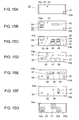
- FIGS. 15A to 15G are exploded views each illustrating a pattern of a dielectric substrate in order from the top while dielectric stacked substrate 30 constituting the left-handed filter according to the fourth embodiment of the present invention is exploded in each dielectric substrate.
- patterns of dielectric substrates are provided in parallel with one another.
- the dielectric substrates illustrated in FIGS. 15A to 15G are sequentially designated by numerals 30a to 30g from the top.
- Dielectric substrates 30a to 30g include input port 31, first output port 32a, second output port 32b, and lateral electrodes 33a and 33b.
- dielectric substrate 30a includes first ground electrode 34.
- dielectric substrate 30g includes second ground electrode 35.
- First ground electrode 34 and second ground electrode 35 are connected to lateral electrodes 33a and 33b to maintain an equal potential.
- Input port 31 and first output port 32a are insulated from first ground electrode 34, second ground electrode 35, and lateral electrodes 33a and 33b.
- input port 31 is connected to conductive pattern 37 on dielectric substrate 30e and conductive pattern 38 on dielectric substrate 30c through via conductor 36.
- Conductive pattern 37 is connected to second ground electrode 35 through via conductor 39.
- Conductive pattern 37 is disposed opposite first ground electrode 34 and second ground electrode 35.
- Conductive pattern 40 is connected on a dielectric substrate identical to a dielectric substrate in which conductive pattern 38 is disposed.
- Conductive pattern 41 is disposed on dielectric substrate 30d different from the dielectric substrate on which conductive pattern 40 is disposed, and conductive pattern 41 is disposed opposite conductive pattern 40 while the dielectric material is interposed therebetween.
- First output port 32a is connected to conductive pattern 43 on dielectric substrate 30f through via conductor 42.
- Conductive pattern 43 is connected to conductive pattern 45 on dielectric substrate 30e, the dielectric substrate on which conductive pattern 45 is disposed, and conductive pattern 46 on dielectric substrate 30c through via conductor 44.
- Conductive pattern 45 is connected to first ground electrode 34 through via conductor 47.
- Conductive pattern 45 is disposed opposite first ground electrode 34 and second ground electrode 35.
- Conductive pattern 48 is connected on dielectric substrate 30c identical to a dielectric substrate on which conductive pattern 46 is disposed.
- Conductive pattern 49 is disposed on dielectric substrate 30d different from the dielectric substrate on which conductive pattern 48 is disposed, and conductive pattern 49 is disposed opposite conductive pattern 48 while the dielectric material is interposed therebetween.
- Second output port 32b is connected to conductive pattern 51 on dielectric substrate 30d through via conductor 50 and to conductive pattern 52 on dielectric substrate 30b different from the dielectric substrate on which conductive pattern 51 is disposed.
- Conductive pattern 51 is connected to first ground electrode 34 through via conductor 53.
- Conductive pattern 51 is disposed opposite first ground electrode 34 and second ground electrode 35.
- Conductive pattern 54 is connected on dielectric substrate 30b identical to a dielectric substrate on which conductive pattern 52 is disposed.
- Conductive pattern 55 is disposed on dielectric substrate 30c different from the dielectric substrate on which conductive pattern 54 is disposed, and conductive pattern 55 is disposed opposite conductive pattern 54 while the dielectric material is interposed therebetween.
- conductive pattern 56 is disposed on dielectric substrate 30b, and conductive pattern 56 is disposed opposite conductive pattern 38 and conductive pattern 46.
- dielectric stacked substrate 30 constituting the left-handed filter illustrated in FIGS. 15A to 15G and the configuration of left-handed resonator 10A illustrated in FIG. 12 will be described below.
- Capacitor 111A that is included in first series body 111 included in first left-handed resonator 10A illustrated in FIG. 12 includes conductive pattern 40 and conductive pattern 41 disposed opposite conductive pattern 40.
- Inductor 111B that is included in first series body 111 included in first left-handed resonator 10A mainly includes conductive pattern 38 and length components of conductive pattern 40 and conductive pattern 41.
- Capacitor 121A that is included in first parallel body 121 included in first left-handed resonator 10A mainly includes conductive pattern 37, first ground electrode 34, and second ground electrode 35. First ground electrode 34 and second ground electrode 35 are disposed opposite conductive pattern 37.
- Inductor 121B that is included in first parallel body 121 included in first left-handed resonator 10A includes via conductor 36 and a length component of conductive pattern 37.
- dielectric stacked substrate 30 constituting the left-handed filter illustrated in FIGS. 15A to 15G and the configuration of the second left-handed resonator 10B illustrated in FIG. 12 will be described below.
- Capacitor 112A that is included in second series body 112 included in second left-handed resonator 10B illustrated in FIG. 12 includes conductive pattern 48 and conductive pattern 49 disposed opposite conductive pattern 48.
- Inductor 112B that is included in second series body 112 included in second left-handed resonator 10B mainly includes length components of conductive pattern 48 and conductive pattern 49.
- Capacitor 122A that is included in second parallel body 122 included in second left-handed resonator 10B mainly includes conductive pattern 45, first ground electrode 34, and second ground electrode 35. First ground electrode 34 and second ground electrode 35 are disposed opposite conductive pattern 45.
- Inductor 122B that is included in second parallel body 122 included in second left-handed resonator 10B includes via conductor 47 and a length component of conductive pattern 45.
- dielectric stacked substrate 30 constituting the left-handed filter illustrated in FIGS. 15A to 15G and the configuration of the third left-handed resonator 10C illustrated in FIG. 12 will be described below.
- Capacitor 113A that is included in third series body 113 included in third left-handed resonator 10C illustrated in FIG. 12 includes conductive pattern 54 and conductive pattern 55 disposed opposite conductive pattern 54.
- Inductor 113B that is included in third series body 113 included in third left-handed resonator 10C mainly includes length components of conductive pattern 54 and conductive pattern 55.
- Capacitor 123A that is included in third parallel body 123 included in third left-handed resonator 10C mainly includes conductive pattern 51, first ground electrode 34, and second ground electrode 35. First ground electrode 34 and second ground electrode 35 are disposed opposite conductive pattern 51.
- Inductor 123B that is included in third parallel body 123 included in third left-handed resonator 10C illustrated in FIG. 12 includes via conductor 53 and a length component of conductive pattern 51.
- the left-handed filter is formed into the structure in which first left-handed resonator 10A, second left-handed resonator 10B, and third left-handed resonator 10C are incorporated in dielectric stacked substrate 30.
- a correspondence relationship among dielectric stacked substrate 30 constituting the left-handed filter illustrated in FIGS. 15A to 15G , the configuration of inter-step coupling element 15 illustrated in FIG. 12 , and the magnetic field coupling between inductor 121B and inductor 123B will be described below.
- Inter-step coupling element 15 illustrated in FIG. 12 has the structure in which conductive pattern 56 is disposed opposite conductive pattern 38 and conductive pattern 46 while the dielectric material is interposed therebetween.
- the magnetic field coupling between inductor 121B and inductor 123B corresponds to the magnetic field coupling between the length component of stacked conductive pattern 37 and the length component of stacked conductive pattern 51.
- the degree of magnetic field coupling can be controlled by adjusting a thickness between dielectric substrate 30d and dielectric substrate 30e to stack dielectric substrate 30d and dielectric substrate 30e.
- the good bandpass characteristic of the balanced-to-unbalanced filter can be obtained in the frequency band of 2.4 to 2.5 GHz used in the wireless LAN.
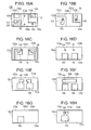
- FIGS. 16A to 16L are exploded views each illustrating a pattern of a dielectric substrate in order from the top while dielectric stacked substrate 130 constituting another left-handed filter according to the fourth embodiment of the present invention is exploded in each dielectric substrate.
- each of the patterns of dielectric substrates is provided in parallel with one another.
- the dielectric substrates illustrated in FIGS. 16A to 16L are sequentially designated by numerals 130a to 130L from the top.
- dielectric substrates 130a to 130L include input port 131, first output port 132a, second output port 132b, and lateral electrodes 133a, 133b, 133c, and 133d (lateral electrodes 133a, 133b, and 133d are insulated from one another).
- dielectric substrate 130a includes first ground electrode 134a.
- dielectric substrate 130b includes second ground electrode 134b.
- dielectric substrate 130k includes third ground electrode 134k.
- dielectric substrate 130L includes fourth ground electrode 134L.
- First ground electrode 134a, second ground electrode 134b, third ground electrode 134k, and fourth ground electrode 134L are each electrically connected to lateral electrodes 133c and 133d to maintain the equal potential.
- First output port 132a and lateral electrode 133a are electrically connected, and second output port 132b and lateral electrode 133b are electrically connected.
- input port 131 is connected to conductive pattern 136 on dielectric substrate 130b through via conductor 135, and conductive pattern 136 is connected to conductive pattern 138 on dielectric substrate 130c through via conductor 137.
- Conductive pattern 138 is connected to first ground electrode 134a, second ground electrode 134b, third ground electrode 134k, and fourth ground electrode 134L through lateral electrode 133c, and conductive pattern 138 is connected to conductive pattern 140 on dielectric substrate 130e through via conductor 139.
- Conductive pattern 140 is disposed opposite conductive pattern 141 on dielectric substrate 130d, and conductive pattern 141 is connected to lateral electrode 133c.
- Conductive pattern 140 is also disposed opposite conductive pattern 142 on dielectric substrate 130f, and conductive pattern 142 is connected to lateral electrode 133c.
- conductive pattern 140 is disposed opposite one end of conductive pattern 143 on dielectric substrate 130f, and the other end of conductive pattern 143 is disposed opposite conductive pattern 144 on dielectric substrate 130e.
- Conductive pattern 144 is disposed opposite conductive pattern 145 on dielectric substrate 130d, and conductive pattern 145 is connected to lateral electrode 133c.
- Conductive pattern 144 is also disposed opposite conductive pattern 146 on dielectric substrate 130f, and conductive pattern 146 is connected to lateral electrode 133c.
- Conductive pattern 144 is connected to conductive pattern 148 on dielectric substrate 130c through via conductor 147, and conductive pattern 148 is connected to lateral electrode 133c. Further, conductive pattern 148 is connected to conductive pattern 150 on dielectric substrate 130b through via conductor 149, and conductive pattern 150 is connected to second output port 132b through via conductor 151.
- Conductive pattern 152 on dielectric substrate 130g which is disposed opposite conductive pattern 142, is disposed opposite conductive pattern 153 on dielectric substrate 130k, and one end of conductive pattern 152 is connected to lateral electrode 133c. Further, conductive pattern 153 is also disposed opposite conductive pattern 154 on dielectric substrate 130i, and one end of conductive pattern 154 is connected to lateral electrode 133c.
- Conductive pattern 153 is connected to conductive pattern 156 on dielectric substrate 130j through via conductor 155, and an end portion of conductive pattern 156 is connected to lateral electrode 133c.
- Conductive pattern 156 is connected to conductive pattern 158 on dielectric substrate 130k through via conductor 157, and conductive pattern 158 is connected to lateral electrode 133a. Further, conductive pattern 158 is connected to first output port 132a through via conductor 159.
- First ground electrode 134a and second ground electrode 134b are connected through via conductor 160, and third ground electrode 134k and fourth ground electrode 134L are connected through via conductor 161.
- dielectric stacked substrate 130 constituting the left-handed filter illustrated in FIGS. 16A to 16L A correspondence relationship between dielectric stacked substrate 130 constituting the left-handed filter illustrated in FIGS. 16A to 16L and the configuration of left-handed resonator 10A illustrated in FIG. 12 will be described below.
- Capacitor 111A that is included in first series body 111 included in first left-handed resonator 10A illustrated in FIG. 12 includes conductive pattern 140 and conductive patterns 141 and 142 disposed opposite conductive pattern 140.
- Inductor 111B that is included in first series body 111 included in first left-handed resonator 10A mainly includes a length component of conductive pattern 140.
- Capacitor 121A that is included in first parallel body 121 included in first left-handed resonator 10A mainly includes conductive pattern 138 and second ground electrode 134b disposed opposite conductive pattern 138.
- Inductor 121B that is included in first parallel body 121 included in first left-handed resonator 10A includes a length component of conductive pattern 138.
- dielectric stacked substrate 130 constituting the left-handed filter illustrated in FIGS. 16A to 16L and the configuration of second left-handed resonator 10B illustrated in FIG. 12 will be described below.
- Capacitor 112A that is included in second series body 112 included in second left-handed resonator 10B illustrated in FIG. 12 includes conductive pattern 144 and conductive patterns 145 and 146 that are disposed opposite conductive pattern 144.
- Inductor 112B that is included in second series body 112 included in second left-handed resonator 10B mainly includes a length component of conductive pattern 144.
- Capacitor 122A that is included in second parallel body 122 included in second left-handed resonator 10B mainly includes conductive pattern 148 and second ground electrode 134b disposed opposite conductive pattern 148.
- Inductor 122B that is included in second parallel body 122 included in second left-handed resonator 10B includes a length component of conductive pattern 148.
- dielectric stacked substrate 130 constituting the left-handed filter illustrated in FIGS. 16A to 16L and the configuration of third left-handed resonator 10C illustrated in FIG. 12 will be described below.
- Capacitor 113A that is included in third series body 113 included in third left-handed resonator 10C illustrated in FIG. 12 mainly includes conductive pattern 153 and conductive patterns 152 and 154 that are disposed opposite conductive pattern 153.
- Inductor 113B that is included in third series body 113 included in third left-handed resonator 10C mainly includes a length component of conductive pattern 153.
- Capacitor 123A that is included in third parallel body 123 included in third left-handed resonator 10C mainly includes conductive pattern 157 and third ground electrode 134k disposed opposite conductive pattern 157.
- Inductor 123B that is included in third parallel body 123 included in third left-handed resonator 10C mainly includes a length component of conductive pattern 156.
- the left-handed filter is formed into the structure in which first left-handed resonator 10A, second left-handed resonator 10B, and third left-handed resonator 10C are incorporated in dielectric stacked substrate 130.
- Inter-step coupling element 15 illustrated in FIG. 12 has the structure in which conductive pattern 143 is disposed opposite conductive pattern 140 and conductive pattern 144 while the dielectric material is interposed therebetween.
- the magnetic field coupling between inductor 121B and inductor 123B corresponds to the magnetic field coupling between the length component of conductive pattern 138 and the length component of conductive pattern 156.
- the degree of the magnetic field coupling can be controlled by adjusting a thickness between dielectric substrate 30d and dielectric substrate 30e to stack dielectric substrate 30d and dielectric substrate 30e.
- Input port 13 of FIG. 12 corresponds to input port 131 of FIG. 16A
- first output port 14A of FIG. 12 corresponds to first output port 132a of FIG. 16A
- second output port 14B of FIG. 12 corresponds to second output port 132b of FIG. 16A
- the left-handed filter illustrated in FIGS. 16A to 16L has the configuration in which third left-handed resonator 10C is disposed above first left-handed resonator 10A, so that the compact left-handed filter can be implemented.
- capacitor 111A and capacitor 113A of FIG. 12 are vertically stacked.
- the signal is outputted from first output port 14A with a phase difference of -90 degrees with respect to the signal supplied to input port 13, and the design is hardly made such that the signal is outputted from second output port 14B with the phase difference of +90 degrees.
- capacitor 111A of FIG. 4 is implemented by the configuration in which conductive pattern 140 of FIG. 16E is sandwiched between conductive patterns 141 and 142 connected to lateral electrode 133c (the electrode connected to the ground).
- capacitor 113A of FIG. 12 is implemented by the configuration in which conductive pattern 144 of FIG. 16E is sandwiched between conductive patterns 145 and 146 connected to lateral electrode 133c (the electrode connected to the ground). Therefore, the coupling between the capacitors can be reduced to implement the easy-to-design left-handed filter.
- the good bandpass characteristic of the balanced-to-unbalanced filter can be obtained in the frequency band of 2.4 to 2.5 GHz used in the wireless LAN.
- FIG. 17 is an equivalent circuit diagram illustrating a left-handed filter according to a sixth embodiment of the present invention.
- the left-handed filter of the seventh embodiment is a filter including input port 613 and output port 614, and inter-step coupling element 617 is interposed between input port 613 and output port 614.
- One end of first series body 611 is electrically connected at connection point 615 between input port 613 and inter-step coupling element 617, and first series body 611 includes capacitor 611A and inductor 611B.
- One end of second series body 6110 is electrically connected at connection point 616 between output port 614 and inter-step coupling element 617, and second series body 6110 includes capacitor 6110A and inductor 6110B.
- first parallel body 612 is electrically connected to the other end of first series body 611, and first parallel body 612 includes capacitor 612A and inductor 612B.
- first parallel body 612 includes capacitor 612A and inductor 612B.
- second parallel body 6120 is electrically connected to the other end of second series body 6110, and second parallel body 6120 includes capacitor 6120A and inductor 6120B.
- the other end of first parallel body 612 is electrically connected to the ground.
- the other end of second parallel body 6120 is electrically connected to the ground.
- First cell 610A includes first series body 611 and first parallel body 612
- second cell 610B includes second series body 6110 and second parallel body 6120.
- Input coupling element 618 is interposed between inter-step coupling element 617 and input port 613, and output coupling element 619 is interposed between inter-step coupling element 617 and output port 614.
- the electromagnetic field coupling is generated between unit cells 610A and 610B.
- first parallel body 612 is connected to the ground through inductor 653 that is of a first parasitic component
- second parallel body 6120 is connected to the ground through inductor 654 serving as a second parasitic component.
- the parallel resonant circuit is equivalently formed by first cell 610A and second cell 610B between which the electromagnetic field coupling is generated and inter-step coupling element 617.
- the impedance of the filter becomes zero when viewed from the input side or the output side, and the frequency at which the signal is passed to the ground exists, so that the number of poles can be increased by one in the passband. As a result, the attenuation characteristic can be improved.
- first parallel body 612 and second parallel body 6120 include inductors 612B and 6120B connected directly to the ground, a large high-frequency current is passed through inductors 612B and 6120B compared with the right-handed filter.
- intensity of the electromagnetic field coupling between unit cells 610A and 610B can be enhanced to increase the number of attenuation poles in the passband, and the frequency can easily be controlled.
- the 0-order resonance coupling between the two unit cells 610A and 610B can easily be controlled by adjusting capacitance values of input coupling element 618, inter-step coupling element 617, and output coupling element 619. Therefore, the left-handed filter in which the passband is formed by the 0-order resonance can be configured. Since the attenuation pole generated by the electromagnetic field coupling between unit cells 610A and 610B and inter-step coupling element 617 can be disposed and controlled, the left-handed filter having more excellent filter characteristic than that of the general left-handed filter can be provided. Not the capacitor, but the inductor may be used as input coupling element 618, inter-step coupling element 617, and output coupling element 619.
- FIG. 18 is an exploded perspective view illustrating a structure of the left-handed filter according to the sixth embodiment of the present invention.
- the left-handed filter has the structure in which the space between grounded conductors 620 and 621 disposed opposite each other is filled with dielectric material 622.
- Conductive pattern 623 corresponds to inductor 611B illustrated in FIG. 17 .
- Conductive pattern 623 and conductive pattern 627 are sandwiched between conductive patterns 624 and 625 that are connected through via conductor 626, thereby forming capacitor 611A illustrated in FIG. 17 .
- Conductive pattern 627 is connected to grounded conductor 621 through via conductor 628, thereby forming inductor 612B illustrated in FIG. 17 .
- Capacitor 612A includes conductive pattern 627 and grounded conductors 620 and 621.
- Capacitor 611A, inductor 611B, capacitor 612A, and inductor 612B correspond to unit cell 610A.
- Unit cells 610B and 610A illustrated in FIG. 17 are formed in a mirror-surface symmetrical manner in relation to line segment A-A' of FIG. 18 , and conductive pattern 629 corresponds to inductor 6110B.
- Conductive pattern 629 and conductive pattern 633 are configured to be sandwiched between conductive patterns 630 and 631 that are connected through via conductor 632, thereby forming capacitor 6110A.
- Conductive pattern 633 is connected to grounded conductor 621 through via conductor 634, thereby forming inductor 6120B.
- Capacitor 6120A includes conductive pattern 633 and grounded conductors 620 and 621.
- Capacitor 6110A, inductor 6110B, capacitor 6120A, and inductor 6120B correspond to unit cell 610B.
- Input coupling element 618 illustrated in FIG. 17 includes a conductive pattern 637 connected through via conductor 636 by input terminal 635 and conductive pattern 623 corresponding to inductor 611B.
- Inter-step coupling element 617 includes conductive pattern 623 constituting a part of unit cell 610A, conductive pattern 629 constituting a part of unit cell 610B, and conductive pattern 638.
- Output coupling element 619 includes conductive pattern 641 connected through via conductor 640 by output terminal 639 and conductive pattern 629 corresponding to inductor 611B.
- via 664 is provided between conductive pattern 627 and grounded conductor 621
- via 671 is provided between conductive pattern 633 and grounded conductor 621.
- the impedance of the filter becomes zero when viewed from the input side or the output side, and the frequency at which the signal is passed to the ground exists, so that the number of poles can be increased by one in the passband.
- the attenuation characteristic can be improved.
- the quarter-wave mode is excited by inductor 653 and unit cell 610A of FIG. 17 , which allows the -1-order mode to be excited by the same number of unit cells as the case in which the 0-order mode is excited. Therefore, the -1-order mode can be excited by half the number of the conventional unit cells. As a result, the no-load Q value can be improved to achieve the miniaturization.
- input coupling element 618 and output coupling element 619 are expressed by the capacitors as illustrated in FIG. 17 . However, when each of the capacitors has a capacitance of 10 pF or more, input coupling element 618 and output coupling element 619 may be removed to directly connect connection points to input port and output port.
- the left-handed filter of the present invention has the effect that the attenuation characteristic can be improved, and the left-handed filter is usefully applied to various electronic instruments such as a cellular telephone.
- FIG. 19 is an equivalent circuit diagram illustrating a left-handed filter according to a seventh embodiment of the present invention.
- the left-handed filter of the seventh embodiment is a filter including input port 713 and output port 714, and inter-step coupling element 717 is interposed between input port 713 and output port 714.
- One end of first parallel body 712 is electrically connected between input port 713 and inter-step coupling element 717, and first parallel body 712 includes capacitor 712A and inductor 712B.
- One end of second parallel body 7120 is electrically connected between output port 714 and inter-step coupling element 717, and second parallel body 7120 includes capacitor 7120A and inductor 7120B.
- first series body 711 is electrically connected to one end of first parallel body 712, and first series body 711 includes capacitor 711A and inductor 711B.
- first series body 711 is electrically connected to one end of second parallel body 7120, and second series body 7110 includes capacitor 7110A and inductor 7110B.
- the other end of first parallel body 712 is electrically connected to the ground.
- the other end of second parallel body 7120 is electrically connected to the ground.
- First cell 710A includes first parallel body 712 and first series body 711
- second cell 710B includes second parallel body 7120 and second series body 7110, and the electromagnetic field coupling is generated between first cell 710A and second cell 710B.
- Input coupling element 718 is interposed between inter-step coupling element 717 and input port 713, and output coupling element 719 is interposed between inter-step coupling element 717 and output port 714.
- first series body 711 is connected to the ground through inductor 753 serving as a first parasitic component
- second series body 7110 is connected to the ground through inductor 754 serving as a second parasitic component.
- the impedance of the filter becomes infinite when the output side is viewed from the input side, and the number of poles can be increased by one in the passband.
- the attenuation characteristic can be improved.
- the quarter-wave mode is excited by inductor 753 and unit cell 710A of FIG. 19 , which allows the -1-order mode to be excited by the same number of unit cells as the case in which the 0-order mode is excited. Therefore, the -1-order mode can be excited by half the number of the conventional unit cells. As a result, the no-load Q value can be improved to achieve the miniaturization.
- first parallel body 712 and first series body 711, and second parallel body 7120 and second series body 7110 constitute the parallel circuits, respectively. Therefore, the passband of the filter can be shifted to the lower side to form the more compact filter.
- the parallel resonant circuit is equivalently formed by first cell 710A and second cell 710B between which the electromagnetic field coupling is generated and inter-step coupling element 717. Accordingly, the impedance of the filter becomes zero when viewed from the input side or the output side, and the frequency at which the signal is passed to the ground exists, so that the number of poles can be increased by one in the passband. As a result, the attenuation characteristic can be improved.
- the 0-order resonance coupling between the two unit cells 710A and 710B can easily be controlled by adjusting capacitance values of input coupling element 718, inter-step coupling element 717, and output coupling element 719. Therefore, the left-handed filter in which the passband is formed by the 0-order resonance can be configured. Since the attenuation pole generated by the electromagnetic field coupling between unit cells 710A and 710B and inter-step coupling element 717 can be disposed and controlled, the left-handed filter having more excellent filter characteristic than that of the general left-handed filter can be provided.
- first parallel body 712 and second parallel body 7120 include inductors 712B and 7120B that are directly connected to the ground, a large high-frequency current is passed through inductors 712B and 7120B compared with the right-handed filter.
- the intensity of the electromagnetic field coupling between unit cells 710A and 710B can be enhanced to increase the number of attenuation poles in the passband, and the frequency can easily be controlled.
- the inductor may be used as input coupling element 718, inter-step coupling element 717, and output coupling element 719.
- FIG. 20 is an exploded perspective view illustrating a structure of the left-handed filter according to the seventh embodiment of the present invention.
- the left-handed filter has the structure in which the space between grounded conductors 720 and 721 disposed opposite each other is filled with dielectric material 722.
- Conductive pattern 723 corresponds to inductor 711B of FIG. 19 .
- Conductive pattern 723 and conductive pattern 727 are sandwiched between conductive patterns 724 and 725 that are connected through via conductor 726, thereby forming capacitor 711A illustrated in FIG. 19 .
- Conductive pattern 727 is connected to grounded conductor 721 through via conductor 728, thereby forming inductor 712B illustrated in FIG. 19 .
- Capacitor 712A includes conductive pattern 727 and grounded conductors 720 and 721.
- Capacitor 711A, inductor 711B, capacitor 712A, and inductor 712B correspond to unit cell 710A.
- Unit cells 710B and 710A illustrated in FIG. 19 are formed in a mirror-surface symmetrical manner in relation to line segment A-A' of FIG. 20 , and conductive pattern 729 corresponds to inductor 7110B.
- Conductive pattern 729 and conductive pattern 733 are configured to be sandwiched between conductive patterns 730 and 731 that are connected through via conductor 732, thereby forming capacitor 7110A.
- Conductive pattern 733 is connected to grounded conductor 721 through via conductor 734, thereby forming inductor 7120B.
- Capacitor 7120A includes conductive pattern 733 and grounded conductors 720 and 721. Capacitor 7110A, inductor 7110B, capacitor 7120A, and inductor 7120B correspond to unit cell 710B.
- Input coupling element 718 illustrated in FIG. 19 includes a conductive pattern 737 that is connected through via conductor 736 by input terminal 735 and conductive pattern 727 corresponding to inductor 712B.
- Inter-step coupling element 717 includes conductive pattern 727 constituting a part of unit cell 710A, conductive pattern 733 constituting a part of unit cell 710B, and conductive pattern 738.
- Output coupling element 719 includes conductive pattern 741 connected through via conductor 740 by output terminal 739 and conductive pattern 733 corresponding to inductor 712B.
- Via 764 is provided between conductive pattern 723 and grounded conductor 721, and via 771 is provided between conductive pattern 729 and grounded conductor 721.
- the parallel resonant circuit is formed by unit cell 710A, and unit cell 710A includes via 764 and conductive pattern 723 constituting inductor 711B illustrated in FIG. 19 , conductive patterns 723, 724, 725, and 727 constituting capacitor 711A and via conductor 726, conductive pattern 727 constituting inductor 712B and via conductor 728, and conductive pattern 727 constituting capacitor 712A and grounded conductors 720 and 721.
- the parallel resonant circuit is also formed by unit cell 710B, and unit cell 710B includes via 771 and conductive pattern 729 constituting inductor 7110B, conductive patterns 729, 730, 731, and 733 constituting capacitor 7110A and via conductor 32, conductive pattern 733 constituting inductor 7120B and via conductor 734, and conductive pattern 723 constituting capacitor 7120A and grounded conductors 720 and 721. Accordingly, the passband of the filter can be shifted to the lower side to implement the more compact filter.
- input coupling element 718 and output coupling element 719 are expressed by the capacitors as illustrated in FIG. 19 . However, when each of the capacitors has the capacitance of 10 pF or more, input coupling element 718 and output coupling element 719 may be removed to directly connect connection points to input port and output port.
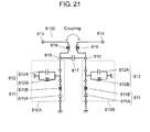
- FIG. 21 is an equivalent circuit diagram of a left-handed filter according to an eighth embodiment of the present invention.
- left-handed filter 8100 of the eighth embodiment includes input port 813, output port 814, inter-step coupling element 817 electrically connected to input port 813 and output port 814, and resonator 810A and resonator 810B that are connected to inter-step coupling element 817.
- Left-handed filter 8100 also includes first inductor 818 that is connected among input port 813, inter-step coupling element 817, and resonator 810A and second inductor 819 that is connected among output port 814, inter-step coupling element 817, and resonator 810B.
- connection point 815 a point at which one end of resonator 810A and one end of inter-step coupling element 817 are connected.
- connection point 816 a point at which one end of resonator 810B and the other end of inter-step coupling element 817 are connected.
- each of resonators 810A and 810B is grounded.
- the other end of each of resonators 810A and 810B may be opened.
- each of resonators 810A and 810B includes one resonator.
- each of resonators 810A and 810B may include a plurality of resonators connected in series.
- Resonator 810A includes parallel body 812 and series body 811.
- Parallel body 812 includes capacitor 812A and inductor 812B, and capacitor 812A and inductor 812B are connected in parallel.
- Series body 811 includes capacitor 811A and inductor 811B, and capacitor 811A and inductor 811B are connected in series.
- one end is connected to one end 815 of inter-step coupling element 817.
- parallel body 812 one end is connected to the other end of series body 811, and the other end is grounded. Since resonator 810B has the same structure as resonator 810A, the description of resonator 810B is omitted.
- series body 811 included in resonator 810A has a configuration in which inductor 811B is connected to parallel body 812 while capacitor 811A is connected to connection point 815.
- series body 811 may have a configuration in which capacitor 811A is connected to parallel body 812 while inductor 811B is connected to connection point 815.
- Resonator 810B may have the similar configuration.
- First inductor 818 is connected between connection point 815 and input port 813.
- Second inductor 819 is connected between connection point 816 and output port 814.
- the disposition relationship between first inductor 818 and second inductor 819 is adjusted such that the magnetic field coupling can be generated between first inductor 818 and second inductor 819. That is, a distance between first inductor 818 and second inductor 819 is shortened.
- the distance between first inductor 818 and second inductor 819 becomes a predetermined value or less, the magnetic field coupling is generated between first inductor 818 and second inductor 819.
- the distance between first inductor 818 and second inductor 819 is more than the predetermined value, the magnetic field coupling is not generated between first inductor 818 and second inductor 819.
- a characteristic of left-handed filter 8100 in generating the magnetic field coupling between first inductor 818 and second inductor 819 will be described below.
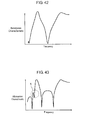
- FIG. 22 is a frequency characteristic diagram when magnetic field coupling between the first inductor 818 and the second inductor 819 is not generated in the left-handed filter according to the eighth embodiment of the present invention.
- FIG. 23 is a frequency characteristic diagram when the magnetic field coupling between the first inductor 818 and the second inductor 819 is generated in the left-handed filter according to the eighth embodiment of the present invention.
- the attenuation pole is newly generated within the passband in the left-handed filter 8100.
- the number of attenuation poles generated in left-handed filter 8100 can be increased by generating the magnetic field coupling between first inductor 818 and second inductor 819. Further, all the attenuation poles including the attenuation poles possessed originally by left-handed filter 8100 can be disposed at any frequency by adjusting the distance between first inductor 818 and second inductor 819. Accordingly, in the left-handed filter of the eighth embodiment, a balance can be established between the improvement of the attenuation characteristic and the adjustment of the attenuation characteristic.
- resonator 810A and resonator 810B are the left-handed resonators that are connected in parallel between input port 813 and output port 814.
- at least three left-handed resonators may be connected in parallel.
- each one inter-step coupling element is connected between the left-handed resonators.
- First inductor 818 is connected among input port 813, the left-handed resonator on the side closest to input port 813, and the inter-step coupling element on the side closest to input port 813.
- Second inductor 819 is connected among output port 814, the left-handed resonator on the side closest to output port 814, and the inter-step coupling element on the side closest to output port 814.
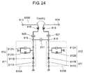
- FIG. 24 is an equivalent circuit diagram of another left-handed filter according to the eighth embodiment of the present invention.
- left-handed filter 8200 further includes input coupling element 820 that is connected between first inductor 818 and connection point 815 and output coupling element 821 that is connected between second inductor 819 and connection point 816.
- input coupling element 820 that is connected between first inductor 818 and connection point 815
- output coupling element 821 that is connected between second inductor 819 and connection point 816.
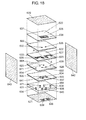
- FIG. 25 is an exploded perspective view illustrating a structure of the left-handed filter according to the eighth embodiment of the present invention.
- left-handed filter 8300 has a structure in which a space between grounded conductor 822 and 823 that are disposed opposite each other is filled with dielectric material 824.
- Input port 825 and output port 826 that are insulated from grounded conductor 823 are provided on the same plane as grounded conductor 823.
- Input port 825 and output port 826 are insulated from each other.
- Conductive pattern 828 is connected to input port 825 through via conductor 827.
- Conductive pattern 828 is connected to conductive pattern 829 and conductive pattern 830, and conductive pattern 828, conductive pattern 829, and conductive pattern 830 are disposed on the same plane.
- Conductive pattern 828 is disposed opposite conductive pattern 831 while dielectric material 824 is interposed therebetween.
- Conductive pattern 829 is disposed opposite conductive pattern 832 while dielectric material 824 is interposed therebetween.
- Conductive pattern 830 is connected to grounded conductor 823 through via conductor 833.
- Conductive pattern 835 is connected to output port 826 through via conductor 834.
- Conductive pattern 835 is connected to conductive pattern 836 and conductive pattern 837, and conductive pattern 835, conductive pattern 836, and conductive pattern 837 are disposed on the same plane. That is, conductive patterns 828, 829, 830, 835, 836, and 837 are disposed on the same plane.
- Conductive pattern 835 is disposed opposite conductive pattern 831 while dielectric material 824 is interposed therebetween.
- Conductive pattern 836 is disposed opposite conductive pattern 838 while dielectric material 824 is interposed therebetween.
- Conductive pattern 837 is connected to grounded conductor 823 through via conductor 839.
- Conductive patterns 831, 832, and 838 are disposed on the same plane.
- Grounded conductors 822 and 823 are connected to lateral electrodes 840 and 841. Accordingly, a potential at grounded conductor 822 is equal to a potential at grounded conductor 823.
- Capacitor 811A of FIG. 21 includes conductive pattern 829 and conductive pattern 832 disposed opposite conductive pattern 829.
- Inductor 811B includes a parasitic inductor possessed by conductive patterns 829 and 832.
- Inductor 812B includes a parasitic inductor possessed by via conductor 833 connected to grounded conductor 823.
- Capacitor 812A mainly includes conductive patterns 829, 830, and 832 and grounded conductors 822 and 823 that are disposed opposite conductive patterns 829, 830, and 832.
- Resonator 810B and resonator 810A are disposed in the line symmetrical manner in relation to line segment A-A', and the configuration of the resonator 810B is similar to that of resonator 810A. Therefore, the description of resonator 810B is omitted.
- Inter-step coupling element 817 is formed by the structure in which conductive pattern 828 and conductive pattern 831 are disposed opposite each other while dielectric material 824 is interposed therebetween and the structure in which conductive pattern 835 and conductive pattern 831 are disposed opposite each other while dielectric material 824 is interposed therebetween.
- First inductor 818 includes a parasitic inductor possessed by via conductor 827.
- Second inductor 819 includes a parasitic inductor possessed by via conductor 834. All the attenuation poles including the attenuation poles possessed originally by left-handed filter 8300 can be disposed at any frequency by adjusting the distance between via conductor 827 and via conductor 834 to stack via conductor 827 and via conductor 834.
- the stacked structure is realized by the above configuration in left-handed filter 8300, it is not necessary to adjust the components of the already-designed left-handed filter.
- the number of attenuation poles generated in left-handed filter 8300 can be increased only by newly providing the inductor while the passband is secured. Further, all the attenuation poles including the attenuation poles possessed originally by left-handed filter 8300 can be disposed at any frequency only by adjusting the distance between the via conductors. Accordingly, it is not necessary to repeat the design. Since the inductor including the via conductor can be accommodated in the space already defined by the design, it is not necessary to secure the new space.
- the compact left-handed filter is maintained, the number of attenuation poles generated is increased while the passband is secured, and all the attenuation poles including the attenuation poles possessed originally by the left-handed filter can be controlled.
- left-handed filter 8300 in which the configuration corresponding to input coupling element 820 or output coupling element 821 is removed can suppress the production cost, maintain the compact left-handed filter, increase the number of attenuation poles generated while the passband is secured, control all the attenuation poles including the attenuation poles possessed originally by left-handed filter 8100, and achieve the further miniaturization.
- the left-handed filter according to the eighth embodiment of the present invention can suppress the production cost, maintain the compact left-handed filter, increase the number of attenuation poles generated while the passband is secured, and control all the attenuation poles including the attenuation poles possessed originally by left-handed filter.
- the left-handed filter of the eighth embodiment is usefully applied to various electronic instruments such as a cellular telephone.
- FIG. 26 is an equivalent circuit illustrating a left-handed filter according to a ninth embodiment of the present invention.
- the left-handed filter of the ninth embodiment is a filter including input port 915 and output port 916, inter-step coupling element 919 is interposed between input port 915 and output port 916, and one end of first series body 911 including capacitor 911A and inductor 911B is electrically connected at connection point 917 between input port 915 and inter-step coupling element 919.
- One end of second series body 9110 including capacitor 9110A and inductor 9110B is electrically connected at connection point 918 between output port 916 and inter-step coupling element 919.
- first parallel body 912 including capacitor 912A and inductor 912B is electrically connected to the other end of first series body 911.
- second parallel body 9120 including capacitor 9120A and inductor 9120B is electrically connected to the other end of second series body 9110.
- the other end of first parallel body 912 is electrically connected to the ground.
- the other end of second parallel body 9120 is electrically connected to the ground.
- First series body 911 and first parallel body 912 constitute first cell 910A
- second series body 9110 and second parallel body 9120 constitute second cell 9100A.
- the other end of first series body 911 is connected to one end of third series body 913 including capacitor 913A and inductor 913B.
- second series body 9110 is connected to one end of fourth series body 9130 including capacitor 9130A and inductor 9130B.
- One end of third parallel body 914 including capacitor 914A and inductor 914B is electrically connected to the other end of third series body 913.
- One end of fourth parallel body 9140 including capacitor 9140A and inductor 9140B is electrically connected to the other end of fourth series body 9130.
- the other end of third parallel body 914 is electrically connected to the ground.
- the other end of fourth parallel body 9140 is electrically connected to the ground.
- Third series body 913 and third parallel body 914 constitute third cell 910B
- fourth series body 9130 and fourth parallel body 9140 constitute fourth cell 9100B.
- Input coupling element 920 is interposed between inter-step coupling element 919 and input port 915, and output coupling element 921 is interposed between inter-step coupling element 919 and output port 916.
- the electromagnetic field coupling is generated between first CRLH resonator 922 including unit cells 910A and 910B and second CRLH resonator 923 including unit cells 9100A and 9100B.
- the -1-order resonance coupling between two CRLH resonators 922 and 923 can easily be controlled by adjusting capacitance values of input coupling element 920, inter-step coupling element 919, and output coupling element 921. Therefore, the left-handed filter in which the passband is formed by the -1-order resonance can be configured. Since the attenuation pole generated by the electromagnetic field coupling between CRLH resonators 922 and 923 and inter-step coupling element 915 can be disposed and controlled, the left-handed filter having more excellent filter characteristic than that of the general left-handed filter can be provided.
- first parallel body 912, second parallel body 9120, third parallel body 914, and fourth parallel body 9140 include inductors 912B, 9120B, 914B, and 9140B that are directly connected to the ground, the large high-frequency current is passed through inductors 912B, 9120B, 914B, and 9140B compared with the right-handed filter.
- the intensity of the electromagnetic field coupling between CRLH resonators 922 and 923 can be enhanced to increase the number of attenuation poles in the passband, and the frequency can easily be controlled.
- the inductor may be used as input coupling element 920, inter-step coupling element 919, and output coupling element 921.
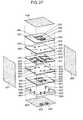
- FIG. 27 is an exploded perspective view illustrating a structure of the left-handed filter according to the ninth embodiment of the present invention.
- the left-handed filter has the structure in which the space between grounded conductors 924 and 925 that are disposed opposite each other is filled with dielectric material 926.
- Conductive pattern 927 corresponds to inductor 911B of FIG. 26 .
- Conductive pattern 927 and conductive pattern 928 are sandwiched between conductive patterns 930 and 931 that are connected through via conductor 929, thereby forming capacitor 912A.
- Conductive pattern 928 is connected to grounded conductor 925 through via conductor 932, thereby forming inductor 912B.
- Capacitor 912A includes conductive pattern 928 and grounded conductors 924 and 925.
- Capacitor 911A, inductor 911B, capacitor 912A, and inductor 912B correspond to unit cell 910A.
- Conductive pattern 928 also corresponds to inductor 913B illustrated in FIG. 26 .
- Conductive pattern 928 and conductive pattern 933 are configured to be sandwiched between conductive patterns 935 and 936 that are connected through via conductor 934, thereby forming capacitor 913A.
- Conductive pattern 933 is connected to grounded conductor 925 through via conductor 937, thereby forming inductor 914B.
- Capacitor 914A illustrated in FIG. 26 includes conductive pattern 933 and grounded conductors 924 and 925.
- Capacitor 913A, inductor 913B, capacitor 914A, and inductor 914B correspond to unit cell 910B.
- Unit cells 910A and 910B constitute first CRLH resonator 922.
- First CRLH resonator 922 and second CRLH resonator 923 illustrated in FIG. 26 are formed in a mirror-surface symmetrical manner in relation to line segment A-A' of FIG. 27 , and conductive pattern 938 corresponds to inductor 9110B.
- Conductive pattern 938 and conductive pattern 939 are configured to be sandwiched between conductive patterns 941 and 942 that are connected through via conductor 940, thereby forming capacitor 9110A.
- Conductive pattern 939 is connected to grounded conductor 925 through via conductor 943, thereby forming inductor 9120B.
- Capacitor 9120A includes conductive pattern 939 and grounded conductors 924 and 925.
- Capacitor 9110A, inductor 9110B, capacitor 9120A, and inductor 9120B correspond to unit cell 9100A.
- Conductive pattern 939 also corresponds to inductor 9130B illustrated in FIG. 26 .
- Conductive pattern 939 and conductive pattern 947 are configured to be sandwiched between conductive patterns 945 and 946 that are connected through via conductor 944, thereby forming capacitor 9130A.
- Conductive pattern 947 is connected to grounded conductor 925 through via conductor 948, thereby forming inductor 9140B.
- Capacitor 9140A includes conductive pattern 947 and grounded conductors 924 and 925.
- Capacitor 9130A, inductor 9130B, capacitor 9140A, and inductor 9140B correspond to unit cell 9100B.
- Unit cells 9100A and 9100B constitute second CRLH resonator 923.
- Input coupling element 920 illustrated in FIG. 26 includes conductive pattern 951 connected through via conductor 950 by input terminal 949 and conductive pattern 927 corresponding to inductor 911B.
- Inter-step coupling element 919 includes conductive pattern 927 constituting a part of unit cell 910A, conductive pattern 938 constituting a part of unit cell 9100A, and conductive pattern 952.
- Output coupling element 921 includes conductive pattern 955 connected through via conductor 954 by output terminal 953 and conductive pattern 938 corresponding to inductor 9110B.
- the electromagnetic field coupling can be generated between first CRLH resonator 922 and second CRLH resonator 923 by incorporating first CRLH resonator 922 and second CRLH resonator 923 in dielectric material 926.
- the attenuation pole can newly be provided by the electromagnetic field coupling and the resonance of inter-step coupling element 919, and the attenuation characteristic can be improved.
- preferably grounded conductors 924 and 925 are connected by lateral electrodes 956 and 957.
- input coupling element 920 and output coupling element 921 are expressed by the capacitors as illustrated in FIG. 26 . However, when each of the capacitors has the capacitance of 10 pF or more, input coupling element 920 and output coupling element 921 may be removed to directly connect connection points to input port and output port.
- FIG. 28 is an equivalent circuit diagram illustrating a left-handed filter according to a tenth embodiment of the present invention.
- the left-handed filter of the tenth embodiment differs from that of the ninth embodiment in that one end of third parallel body 1014 is connected to the ground through inductor 1058 serving as a first parasitic component and one end of fourth parallel body 10140 is connected to the ground through inductor 1059 serving as a second parasitic component.
- the configuration similar to that of the ninth embodiment is designated by the same numeral, and the description thereof is omitted.
- FIG. 29 is an exploded perspective view illustrating a structure of the left-handed filter according to the tenth embodiment of the present invention.
- via conductor 1060 is provided between conductive pattern 1033 and grounded conductor 1025, and via conductor 1061 is provided between conductive pattern 1047 and grounded conductor 1025.
- the 0- order resonance in which the unnecessary passband is formed can be shifted onto the high-frequency side.
- the left-handed filter of the present invention has the effect that the attenuation characteristic can be improved, and the left-handed filter can usefully be applied to various electronic instruments such as a cellular telephone.
- FIG. 30 is an equivalent circuit diagram illustrating a left-handed filter according to an eleventh embodiment of the present invention.
- the left-handed filter of the eleventh embodiment is a filter including input port 1115 and output port 1116, inter-step coupling element 1119 is interposed between input port 1115 and output port 1116, and one end of first parallel body 1112 including capacitor 1112A and inductor 1112B is electrically connected at connection point 1117 between input port 1115 and inter-step coupling element 1119.
- One end of second parallel body 11120 including capacitor 11120A and inductor 11120B is electrically connected at connection point 1118 between output port 1116 and inter-step coupling element 1119.
- first series body 1111 including capacitor 1111A and inductor 1111B is electrically connected to one end of first parallel body 1112.
- second series body 11110 including capacitor 11110A and inductor 11110B is electrically connected to one end of second parallel body 11120.
- the other end of first parallel body 1112 is electrically connected to the ground.
- the other end of second parallel body 11120 is electrically connected to the ground.
- First series body 1111 and first parallel body 1112 constitute first cell 1110A
- second series body 11110 and second parallel body 11120 constitute second cell 11100A.
- the other end of first series body 1111 is connected to one end of third parallel body 1114 including capacitor 1114A and inductor 1114B.
- second series body 11110 is connected to one end of fourth parallel body 11140 including capacitor 11140A and inductor 11140B.
- One end of third series body 1113 is electrically connected to one end of third parallel body 1114 including capacitor 1113A and inductor 1113B.
- One end of fourth series body 11130 including capacitor 11130A and inductor 11130B is electrically connected to one end of fourth parallel body 11140.
- the other end of third parallel body 1114 is electrically connected to the ground.
- the other end of fourth parallel body 11140 is electrically connected to the ground.
- Third series body 1113 and third parallel body 1114 constitute third cell 1110B
- fourth series body 11130 and fourth parallel body 11140 constitute fourth cell 11100B.
- Input coupling element 1120 is interposed between inter-step coupling element 1119 and input port 1115, and output coupling element 1121 is interposed between inter-step coupling element 1119 and output port 1116.
- the electromagnetic field coupling is generated between first CRLH resonator 1122 including unit cells 1110A and 1110B and second CRLH resonator 1123 including unit cells 11100A and 11100B.
- the parallel resonant circuit is equivalently formed by first CRLH resonator 1122 and second CRLH resonator 1123 between which the electromagnetic field coupling is generated and inter-step coupling element 1119. Therefore, the impedance of the filter becomes zero when viewed from the input side or output side, and the frequency at which the signal is passed to the ground exists, so that the number of poles can be increased by one in the passband. As a result, the attenuation characteristic can be improved.
- the -1-order resonance coupling between two CRLH resonators 1122 and 1123 can easily be controlled by adjusting capacitance values of input coupling element 1120, inter-step coupling element 1119, and output coupling element 1121. Therefore, the left-handed filter in which the passband is formed by the -1-order resonance can be configured. Since the attenuation pole generated by the electromagnetic field coupling between CRLH resonators 1122 and 1123 and inter-step coupling element 1119 can be disposed and controlled, the left-handed filter having more excellent filter characteristic than that of the general left-handed filter can be provided.
- first parallel body 1112, second parallel body 11120, third parallel body 1114, and fourth parallel body 11140 include inductors 1112B, 11120B, 1114B, and 11140B that are directly connected to the ground, the large high-frequency current is passed through inductors 1112B, 11120B, 1114B, and 11140B compared with the right-handed filter.
- the intensity of the electromagnetic field coupling between CRLH resonators 1122 and 1123 can be enhanced to increase the number of attenuation poles in the passband, and the frequency can easily be controlled.
- the inductor may be used as input coupling element 1120, inter-step coupling element 1119, and output coupling element 1121.
- FIG. 31 is an exploded perspective view illustrating a structure of the left-handed filter according to the eleventh embodiment of the present invention.
- the left-handed filter has the structure in which the space between grounded conductors 1124 and 1125 that are disposed opposite each other is filled with dielectric material 1126.
- Conductive pattern 1127 is connected to grounded conductor 1125 through via conductor 1132.
- Conductive pattern 1127 corresponds to inductor 1112B of FIG. 30 .
- grounded conductors 1124 and 1125 constitute capacitor 1112A.
- Conductive pattern 1127 and conductive pattern 1128 are sandwiched between conductive patterns 1130 and 1131 that are connected through via conductor 1129, thereby forming capacitor 1111A.
- Conductive pattern 1128 also corresponds to inductor 1111B illustrated in FIG. 30 .
- Capacitor 1111A, inductor 1111B, capacitor 1112A, and inductor 1112B correspond to unit cell 1110A.
- Conductive pattern 1128 is connected to grounded conductor 1125 through via conductor 1137, thereby forming inductor 1114B illustrated in FIG. 30 .
- capacitor 1114A includes conductive pattern 1133 and grounded conductors 1124 and 1125.
- Conductive pattern 1128 and conductive pattern 1133 are configured to be sandwiched between conductive patterns 1135 and 1136 that are connected through via conductor 1134, thereby forming capacitor 1113A.
- Conductive pattern 1133 also corresponds to inductor 1113B.
- Capacitor 1113A, inductor 1113B, capacitor 1114A, and inductor 1114B correspond to unit cell 1110B.
- Unit cells 1110A and 1110B constitute first CRLH resonator 1122.
- First CRLH resonator 1122 and second CRLH resonator 1123 illustrated in FIG. 30 are formed in a mirror-surface symmetrical manner in relation to line segment A-A' of FIG. 31 , and conductive pattern 1138 is connected to grounded conductor 1125 through via conductor 1143.
- Conductive pattern 1138 corresponds to inductor 11120B.
- grounded conductors 1124 and 1125 constitute capacitor 11120A.
- Conductive pattern 1138 and conductive pattern 1139 are configured to be sandwiched between conductive patterns 1141 and 1142 that are connected through via conductor 1140, thereby forming capacitor 11110A.
- Conductive pattern 1139 also corresponds to inductor 11110B.
- Capacitor 11110A, inductor 11110B, capacitor 11120A, and inductor 11120B correspond to unit cell 11100A.
- Conductive pattern 1139 is connected to grounded conductor 1125 through via conductor 1148, thereby forming inductor 11140B illustrated in FIG. 30 .
- Capacitor 11140A includes conductive pattern 1139 and grounded conductors 1124 and 1125.
- Conductive pattern 1139 and conductive pattern 1147 are configured to be sandwiched between conductive patterns 1145 and 1146 that are connected through via conductor 1144, thereby forming capacitor 11130A.
- Conductive pattern 1147 also corresponds to inductor 11130B.
- Capacitor 11130A, inductor 11130B, capacitor 11140A, and inductor 11140B correspond to unit cell 11100B.
- Unit cells 11100A and 11100B constitute second CRLH resonator 1123.
- Input coupling element 1120 illustrated in FIG. 30 includes a conductive pattern 1151 that is connected through via conductor 1150 by input terminal 1149 and conductive pattern 1127 corresponding to inductor 1112B.
- Inter-step coupling element 1119 includes conductive pattern 1127 constituting a part of unit cell 1110A, conductive pattern 1138 constituting a part of unit cell 11100A, and conductive pattern 1152.
- Output coupling element 1121 illustrated in FIG. 30 includes conductive pattern 1155 that is connected through via conductor 1154 by output terminal 1153 and conductive pattern 1138 corresponding to inductor 11120B.
- FIG. 32 is a frequency characteristic diagram of the left-handed filter of the eleventh embodiment.
- the electromagnetic field coupling can be generated between first CRLH resonator 1122 and second CRLH resonator 1123 by incorporating first CRLH resonator 1122 and second CRLH resonator 1123 in dielectric material 1126. Therefore, the attenuation pole can newly be provided by the electromagnetic field coupling and the resonance of inter-step coupling element 1119, and the attenuation characteristic can be improved.
- preferably grounded conductors 1124 and 1125 are connected by lateral electrodes 1156 and 1157.
- input coupling element 1120 and output coupling element 1121 are expressed by the capacitors as illustrated in FIG. 30 . However, when each of the capacitors has the capacitance of 10 pF or more, input coupling element 1120 and output coupling element 1121 may be removed to directly connect connection points to input port and output port.
- FIG. 33 is an equivalent circuit diagram illustrating a left-handed filter according to a twelfth embodiment of the present invention.
- the left-handed filter of the twelfth embodiment differs from that of the eleventh embodiment in that the other end of third series body 1213 is connected to the ground through inductor 1258 serving as a first parasitic component and the other end of fourth series body 12130 is connected to the ground through inductor 1259 that is of a second parasitic component.
- the configuration similar to that of the eleventh embodiment is designated by the same numeral, and the description thereof is omitted.
- FIG. 34 is an exploded perspective view illustrating a structure of the left-handed filter according to the twelfth embodiment of the present invention.
- via conductor 1260 is provided between conductive pattern 1233 and grounded conductor 1225
- via conductor 1261 is provided between conductive pattern 1247 and grounded conductor 1225.
- the left-handed filter has the characteristic of the eleventh embodiment, and the 0-order resonance at which the unnecessary passband is formed can be shifted onto the high-frequency side.
- FIG. 35 is an equivalent circuit diagram illustrating a left-handed filter according to a thirteenth embodiment of the present invention.
- the left-handed filter of the thirteenth embodiment is a filter including input port 1315, first output port 1316A, and second output port 1316B, inter-step coupling element 1319A is interposed between input port 1315 and first output port 1316A, and one end of first series body 1311 including capacitor 1311A and inductor 1311B is electrically connected at connection point 1317 between input port 1315 and inter-step coupling element 1319A.
- One end of second series body 13110 including capacitor 13110A and inductor 13110B is electrically connected at connection point 1318 between first output port 1316A and inter-step coupling element 1319A.
- One end of first parallel body 1312 including capacitor 1312A and inductor 1312B is electrically connected to one end of first series body 1311.
- One end of second parallel body 13120 including capacitor 13120A and inductor 13120B is electrically connected to one end of second series body 13110.
- the other end of first parallel body 1312 is electrically connected to the ground.
- the other end of second parallel body 13120 is electrically connected to the ground.
- First series body 1311 and first parallel body 1312 constitute first cell 1310A
- second series body 13110 and second parallel body 13120 constitute second cell 13100A.
- first series body 1311 is connected to one end of third series body 1313 including capacitor 1313A and inductor 1313B.
- the other end of second series body 13110 is connected to one end of fourth series body 13130 including capacitor 13130A and inductor 13130B.
- One end of third parallel body 1314 including capacitor 1314A and inductor 1314B is electrically connected to one end of third series body 1313.
- One end of fourth parallel body 13140 including capacitor 13140A and inductor 13140B is electrically connected to one end of fourth series body 13130.
- the other end of third parallel body 1314 is electrically connected to the ground.
- the other end of fourth parallel body 13140 is electrically connected to the ground.
- Third series body 1313 and third parallel body 1314 constitute third cell 1310B
- fourth series body 13130 and fourth parallel body 13140 constitute fourth cell 13100B.
- Input coupling element 1320 is interposed between inter-step coupling element 1319A and input port 1315.
- Output coupling element 1321A is interposed between inter-step coupling element 1319A and first output port 1316A.
- Inter-step coupling element 1319B is interposed between the other end of third cell 1310B and the other end of fourth cell 13100B.
- Output coupling element 1321B is interposed between the other end of fourth cell 13100B and second output port 1316B.
- the electromagnetic field coupling is generated between first CRLH resonator 1322 including unit cells 1310A and 1310B and second CRLH resonator 1323 including unit cells 13100A and 13100B. Since the parallel resonant circuit is equivalently formed by first CRLH resonator 1322 and second CRLH resonator 1323 between which the electromagnetic field coupling is generated and inter-step coupling elements 1319A and 1319B, the impedance of the filter becomes zero when viewed from the input side or output side. The frequency at which the signal is passed to the ground exists, so that the number of poles can be increased by one in the passband. As a result, the attenuation characteristic can be improved.
- the -1-order resonance coupling between two CRLH resonators 1322 and 1323 can easily be controlled by adjusting capacitance values of input coupling element 1320, inter-step coupling elements 1319A and 1319B, and output coupling elements 1321A and 1321B. Therefore, the left-handed filter in which the passband is formed by the -1-order resonance can be configured. Since the attenuation pole generated by the electromagnetic field coupling between CRLH resonators 1322 and 1323 and inter-step coupling element 1315 can be disposed and controlled, the left-handed filter having more excellent filter characteristic than that of the general left-handed filter can be provided.
- first parallel body 1312, second parallel body 13120, third parallel body 1314, and fourth parallel body 13140 include inductors 1312B, 13120B, 1314B, and 13140B that are directly connected to the ground, a large high-frequency current is passed through inductors 1312B, 13120B, 1314B, and 13140B compared with the right-handed filter.
- the intensity of the electromagnetic field coupling between CRLH resonators 1322 and 1323 can be enhanced to increase the number of attenuation poles in the passband, and the frequency can easily be controlled.
- the inductor may be used as input coupling element 1320, inter-step coupling elements 1319A and 1319B, and output coupling elements 1321A and 1321B.
- FIG. 36 is an exploded perspective view illustrating a structure of the left-handed filter according to the thirteenth embodiment of the present invention.
- the left-handed filter has the structure in which the space between grounded conductors 1324 and 1325 that are disposed opposite each other is filled with dielectric material 1326.
- Conductive pattern 1327 corresponds to inductor 1311B of FIG. 35 .
- Conductive pattern 1327 and conductive pattern 1328 are sandwiched between conductive patterns 1330 and 1331 that are connected through via conductor 1329, thereby forming capacitor 1311A.
- Conductive pattern 1328 is connected to grounded conductor 1325 through via conductor 1332.
- Conductive pattern 1328 corresponds to inductor 1312B.
- Capacitor 1312A includes conductive pattern 1328 and grounded conductors 1324 and 1325.
- Capacitor 1311A, inductor 1311B, capacitor 1312A, and inductor 1312B correspond to unit cell 1310A.
- Conductive pattern 1328 also corresponds to inductor 1313B illustrated in FIG. 35 .
- Conductive pattern 1328 and conductive pattern 1333 are configured to be sandwiched between conductive patterns 1335 and 1336 that are connected through via conductor 1334, thereby forming capacitor 1313A.
- Conductive pattern 1333 is connected to grounded conductor 1325 through via conductor 1337, thereby forming inductor 1314B.
- Capacitor 1314A includes conductive pattern 1333 and grounded conductors 1324 and 1325.
- Capacitor 1313A, inductor 1313B, capacitor 1314A, and inductor 1314B correspond to unit cell 1310B.
- Unit cells 1310A and 1310B constitute first CRLH resonator 1322.
- First CRLH resonator 1322 and second CRLH resonator 1323 illustrated in FIG. 35 are formed in a mirror-surface symmetrical manner in relation to line segment A-A' of FIG. 36 , and conductive pattern 1338 corresponds to inductor 13110B.
- Conductive pattern 1338 and conductive pattern 1339 are configured to be sandwiched between conductive patterns 1341 and 1342 that are connected through via conductor 1340, thereby forming capacitor 13110A.
- Conductive pattern 1339 is connected to grounded conductor 1325 through via conductor 134.
- Conductive pattern 1339 corresponds to inductor 13120B.
- Capacitor 13120A includes conductive pattern 1339 and grounded conductors 1324 and 1325.
- Capacitor 13110A, inductor 13110B, capacitor 13120A, and inductor 13120B correspond to unit cell 13100A.
- Conductive pattern 1339 also corresponds to inductor 13130B illustrated in FIG. 35 .
- Conductive pattern 1339 and conductive pattern 1347 are configured to be sandwiched between conductive patterns 1345 and 1346 that are connected through via conductor 1344, thereby forming capacitor 13130A.
- Conductive pattern 1347 is connected to grounded conductor 1325 through via conductor 1348, thereby forming inductor 13140B.
- capacitor 13140A includes conductive pattern 1347 and grounded conductors 1324 and 1325.
- Capacitor 13130A, inductor 13130B, capacitor 13140A, and inductor 13140B correspond to unit cell 13100B.
- Unit cells 13100A and 13100B constitute second CRLH resonator 1323.
- Input coupling element 1320 illustrated in FIG. 35 includes conductive pattern 1356 that is connected through via conductor 1355 by input terminal 1354 and conductive pattern 1338 corresponding to inductor 13120B.
- Inter-step coupling element 1319A includes conductive pattern 1327 constituting a part of unit cell 1310A, conductive pattern 1338 constituting a part of unit cell 13100A, and conductive pattern 1352.
- Inter-step coupling element 1319B includes conductive pattern 1333 corresponding to inductor 1314B, conductive pattern 1347 corresponding to inductor 13140B, and conductive pattern 1353.
- Output coupling element 1321A includes conductive pattern 1351 that is connected through via conductor 1350 by first output terminal 1349 and conductive pattern 1327 corresponding to inductor 1312B.
- Output coupling element 1321B includes conductive pattern 1359 that is connected through via conductor 1358 by second output terminal 1357 and conductive pattern 1347 corresponding to inductor 13140B.
- FIG. 37 is a frequency characteristic diagram of the left-handed filter according to the thirteenth embodiment of the present invention.
- the electromagnetic field coupling is generated between first CRLH resonator 1322 and second CRLH resonator 1323 by incorporating first CRLH resonator 1322 and second CRLH resonator 1323 in dielectric material 1326.
- the attenuation pole can newly be provided by the electromagnetic field coupling and the resonance of inter-step coupling element 1319, and the attenuation characteristic can be improved.
- preferably grounded conductors 1324 and 1325 are connected by lateral electrodes 1360 and 1361.
- input coupling element 1320 and output coupling elements 1321A and 1321B are expressed by the capacitors as illustrated in FIG. 35 .
- input coupling element 1320 and output coupling elements 1321A and 1321B may be removed to directly connect the connection points to the input port and the output port.
- the left-handed filter of the present invention has the effect that the attenuation characteristic can be improved, and the left-handed filter can usefully be applied to various electronic instruments such as a cellular telephone.
- FIG. 38 is an equivalent circuit diagram illustrating a left-handed filter according to a fourteenth embodiment of the present invention.
- the left-handed filter of the fourteenth embodiment is a filter including input port 1415, first output port 1416A, and second output port 1416B, inter-step coupling element 1419A is interposed between input port 1415 and first output port 1416A, and one end of first series body 1411 including capacitor 1411A and inductor 1411B is electrically connected at connection point 1417 between input port 1415 and inter-step coupling element 1419A.
- One end of second series body 14110 including capacitor 14110A and inductor 14110B is electrically connected at connection point 1418 between first output port 1416A and inter-step coupling element 1419A.
- first parallel body 1412 including capacitor 1412A and inductor 1412B is electrically connected to one end of first series body 1411.
- second parallel body 14120 including capacitor 14120A and inductor 14120B is electrically connected to one end of second series body 14110.
- the other end of first parallel body 1412 is electrically connected to the ground.
- the other end of second parallel body 14120 is electrically connected to the ground.
- First series body 1411 and first parallel body 1412 constitute first cell 1410A
- second series body 14110 and second parallel body 14120 constitute second cell 14100A.
- first series body 1411 is connected to one end of third series body 1413 including capacitor 1413A and inductor 1413B.
- second series body 14110 is connected to one end of fourth series body 14130 including capacitor 14130A and inductor 14130B.
- One end of third parallel body 1414 including capacitor 1414A and inductor 1414B is electrically connected to one end of third series body 1413.
- One end of fourth parallel body 14140 including capacitor 14140A and inductor 14140B is electrically connected to one end of fourth series body 14130.
- third parallel body 1414 is electrically connected to the ground.
- fourth parallel body 14140 is electrically connected to the ground.
- Third series body 1413 and third parallel body 1414 constitute third cell 1410B, and fourth series body 14130 and fourth parallel body 14140 constitute fourth cell 14100B.
- Input coupling element 1420 is interposed between inter-step coupling element 1419A and input port 1415.
- Output coupling element 1421A is interposed between inter-step coupling element 1419A and first output port 1416A.
- Inter-step coupling element 1419B is interposed between the other end of third cell 1410B and the other end of fourth cell 14100B.
- Output coupling element 1421B is interposed between the other end of fourth cell 14100B and second output port 1416B.
- first CRLH resonator 1422 including unit cells 1410A and 1410B and second
- CRLH resonator 1423 including unit cells 14100A and 14100B. Since the parallel resonant circuit is equivalently formed by first CRLH resonator 1422 and second CRLH resonator 1423 between which the electromagnetic field coupling is generated and inter-step coupling elements 1419A and 1419B, the impedance of the filter becomes zero when viewed from the input side or output side. The frequency at which the signal is passed to the ground exists, so that the number of poles can be increased by one in the passband. As a result, the attenuation characteristic can be improved.
- the -1-order resonance coupling between two CRLH resonators 1422 and 1423 can easily be controlled by adjusting capacitance values of input coupling element 1420, inter-step coupling elements 1419A and 1419B, and output coupling elements 1421A and 1421B. Therefore, the left-handed filter in which the passband is formed by the -1-order resonance can be configured. Since the attenuation pole generated by the electromagnetic field coupling between CRLH resonators 1422 and 1423 and inter-step coupling elements 1419A and 1419B can be disposed and controlled, the left-handed filter having more excellent filter characteristic than that of the general left-handed filter can be provided.
- first parallel body 1412, second parallel body 14120, third parallel body 1414, and fourth parallel body 14140 include inductors 1412B, 14120B, 1414B, and 14140B that are directly connected to the ground, the large high-frequency current is passed through inductors 1412B, 14120B, 1414B, and 14140B compared with the right-handed filter.
- the intensity of the electromagnetic field coupling between CRLH resonators 1422 and 1423 can be enhanced to increase the number of attenuation poles in the passband, and the frequency can easily be controlled.
- the inductor may be used as input coupling element 1420, inter-step coupling elements 1419A and 1419B, and output coupling elements 1421A and 1421B.
- FIG. 39 is an exploded perspective view illustrating a structure of the left-handed filter according to the fourteenth embodiment of the present invention.
- the left-handed filter has the structure in which the space between grounded conductors 1424 and 1425 that are disposed opposite each other is filled with dielectric material 1426, and conductive pattern 1427 is connected to grounded conductor 1425 through via conductor 1432. Further, conductive pattern 1427 corresponds to inductor 1412B of FIG. 38 .
- grounded conductor 1424 and 1425 constitute capacitor 1412A.
- Conductive pattern 1427 and conductive pattern 1428 are sandwiched between conductive patterns 1430 and 1431 that are connected through via conductor 1429, thereby forming capacitor 1411A.
- Conductive pattern 1428 also corresponds to inductor 1411B.
- Capacitor 1411A, inductor 1411B, capacitor 1412A, and inductor 1412B correspond to unit cell 1410A.
- Conductive pattern 1428 is connected to grounded conductor 1425 through via conductor 1437, thereby forming inductor 1414B illustrated in FIG. 38 .
- conductive pattern 1428 conductive pattern 1433 and grounded conductors 1424 and 1425 constitute capacitor 1414A.
- Conductive pattern 1428 and conductive pattern 1433 are sandwiched between conductive patterns 1435 and 1436 that are connected through via conductor 1434, thereby forming capacitor 1413A.
- Conductive pattern 1433 also corresponds to inductor 1413B.
- Capacitor 1413A, inductor 1413B, capacitor 1414A, and inductor 1414B correspond to unit cell 1410B.
- Unit cells 1410A and 1410B constitute first CRLH resonator 1422.
- First CRLH resonator 1422 and second CRLH resonator 1423 illustrated in FIG. 38 are formed in a mirror-surface symmetrical manner in relation to line segment A-A' of FIG. 39 , and conductive pattern 1438 is connected to grounded conductor 1425 through via conductor 1443.
- Conductive pattern 1438 corresponds to inductor 14120B.
- grounded conductor 1424 and 1425 constitute capacitor 14120A.
- Conductive pattern 1438 and conductive pattern 1439 are configured to be sandwiched between conductive patterns 1441 and 1442 that are connected through via conductor 1440, thereby forming capacitor 14110A.
- Conductive pattern 1439 also corresponds to inductor 14110B.
- Capacitor 14110A, inductor 14110B, capacitor 14120A, and inductor 14120B correspond to unit cell 14100A.
- Conductive pattern 1439 is connected to grounded conductor 1425 through via conductor 1448, thereby forming inductor 14140B illustrated in FIG. 38 .
- Capacitor 14140A includes conductive pattern 1439 and grounded conductors 1424 and 1425.
- Conductive pattern 1439 and conductive pattern 1447 are configured to be sandwiched between conductive patterns 1445 and 1446 that are connected through via conductor 1444, thereby forming capacitor 14130A.
- Conductive pattern 1447 also corresponds to inductor 14130B.
- Capacitor 14130A, inductor 14130B, capacitor 14140A, and inductor 14140B correspond to unit cell 14100B.
- Unit cells 14100A and 14100B constitute second CRLH resonator 1423.
- Input coupling element 1420 illustrated in FIG. 38 includes conductive pattern 1451 connected through via conductor 1450 by input terminal 1449 and conductive pattern 1427 corresponding to inductor 1412B.
- Inter-step coupling element 1419A includes conductive pattern 1427 constituting a part of unit cell 1410A, conductive pattern 1438 constituting a part of unit cell 14100A, and conductive pattern 1452.
- Inter-step coupling element 1419B includes conductive pattern 1433 corresponding to inductor 1413B, conductive pattern 1447 corresponding to inductor 14130B, and conductive pattern 1453.
- Output coupling element 1421A includes conductive pattern 1456 that is connected through via conductor 1455 by first output terminal 1454 and conductive pattern 1438 corresponding to inductor 14120B.
- Output coupling element 1421B includes conductive pattern 1459 that is connected through via conductor 1458 by second output terminal 1457 and conductive pattern 1447 corresponding to inductor 14130B.
- FIG. 40 is a frequency characteristic diagram of the left-handed filter according to the fourteenth embodiment of the present invention.
- the electromagnetic field coupling is generated between first CRLH resonator 1422 and second CRLH resonator 1423 by incorporating first CRLH resonator 1422 and second CRLH resonator 1423 in dielectric material 1426.
- the attenuation pole can newly be provided by the electromagnetic field coupling and the resonance of inter-step coupling element 1419, and the attenuation characteristic can be improved.
- preferably grounded conductors 1424 and 1425 are connected by lateral electrodes 1460 and 1461.
- input coupling element 1420 and output coupling elements 1421A and 1421B are expressed by the capacitors as illustrated in FIG. 38 . However, when each of the capacitors has the capacitance of 10 pF or more, input coupling element 1420 and output coupling elements 1421A and 1421B may be removed to directly connect the connection points to the input port and the output port.
- the left-handed filter of the present invention has the effect that the attenuation characteristic can be improved, and the left-handed filter can usefully be applied to various electronic instruments such as a cellular telephone.
- FIG. 41 is an equivalent circuit diagram of a left-handed filter according to a fifteenth embodiment of the present invention.
- left-handed filter 15100 of the fifteenth embodiment includes input port 1513, output port 1514, first inter-step coupling element 1517 electrically connected to input port 1513 and output port 1514, second inter-step coupling element 1520, and third inter-step coupling element 1521.
- Left-handed filter 15100 also includes first left-handed resonator 1510A connected to first inter-step coupling element 1517 and second inter-step coupling element 1520, second left-handed resonator 1510B connected to first inter-step coupling element 1517 and third inter-step coupling element 1521, and third left-handed resonator 1510C connected to second inter-step coupling element 1520 and third inter-step coupling element 1521.
- Left-handed filter 15100 also includes first inductor 1518 that is connected among input port 1513, first inter-step coupling element 1517, second inter-step coupling element 1520, and first left-handed resonator 1510A and second inductor 1519 that is connected among output port 1514, first inter-step coupling element 1517, third inter-step coupling element 1521, and second left-handed resonator 1510B.
- first left-handed resonator 1510A one end is connected to one end of first inter-step coupling element 1517 and one end of second inter-step coupling element 1520, and the other end is grounded.
- connection point 1515 a point at which one end of first left-handed resonator 1510A, one end of first inter-step coupling element 1517, and one end of second inter-step coupling element 1520 are connected.
- second left-handed resonator 1510B one end is connected to the other end of first inter-step coupling element 1517 and one end of third inter-step coupling element 1521, and the other end is grounded.
- connection point 1516 a point at which one end of second left-handed resonator 1510B, the other end of first inter-step coupling element 1517, and one end of third inter-step coupling element 1521 are connected is defined as connection point 1516.
- third left-handed resonator 1510C one end is connected to the other end of second inter-step coupling element 1520 and the other end of third inter-step coupling element 1521, and the other end is grounded.
- each of first left-handed resonator 1510A, second left-handed resonator 1510B, and third left-handed resonator 1510C is grounded.
- the other end of each of first left-handed resonator 1510A, second left-handed resonator 1510B, and third left-handed resonator 1510C may be opened.
- each of first left-handed resonator 1510A, second left-handed resonator 1510B, and third left-handed resonator 1510C includes one left-handed resonator.
- each of first left-handed resonator 1510A, second left-handed resonator 1510B, and third left-handed resonator 1510C may include a plurality of left-handed resonators that are connected in series.
- First left-handed resonator 1510A includes parallel body 15121 and series body 15111.
- Parallel body 15121 includes capacitor 15121A and inductor 15121B, and capacitor 15121A and inductor 15121B are connected in parallel.
- Series body 15111 includes capacitor 15111A and inductor 15111B, and capacitor 15111A and inductor 15111B are connected in series.
- one end is connected to one end of first inter-step coupling element 1517 and one end of second inter-step coupling element 1520.
- parallel body 15121 one end is connected to the other end of series body 15111, and the other end is grounded.
- Second left-handed resonator 1510B includes parallel body 15122 and series body 15112.
- Parallel body 15122 includes capacitor 151212A and inductor 15122B, and capacitor 15122A and inductor 15122B are connected in parallel.
- Series body 15112 includes capacitor 15112A and inductor 15112B, and capacitor 15112A and inductor 15112B are connected in series.
- one end is connected to the other end of first inter-step coupling element 1517 and one end of third inter-step coupling element 1521.
- parallel body 15122 one end is connected to the other end of series body 15112, and the other end is grounded.
- Third left-handed resonator 1510C includes parallel body 15123 and series body 15113.
- Parallel body 15123 includes capacitor 15123A and inductor 15123B, and capacitor 15123A and inductor 15123B are connected in parallel.
- Series body 15113 includes capacitor 15113A and inductor 15113B, and capacitor 15113A and inductor 15113B are connected in series.
- one end is connected to the other end of second inter-step coupling element 1520 and the other end of third inter-step coupling element 1521.
- parallel body 15123 one end is connected to the other end of series body 15113, and the other end is grounded.
- series body 15111 included in first left-handed resonator 1510A has the configuration in which inductor 15111B is connected to parallel body 15121 while capacitor 15111A is connected to connection point 1515.
- series body 15111 may have a configuration in which capacitor 15111A is connected to parallel body 15121 while inductor 15111B is connected to connection point 1515.
- Second left-handed resonator 1510B and third left-handed resonator 1510C may have the similar configuration.
- First inductor 1518 is connected between connection point 1515 and input port 1513.
- Second inductor 1519 is connected between connection point 1516 and output port 1514.
- a disposition relationship among first inductor 1518, second inductor 1519, and inductor 15123B of parallel body 15123 of third left-handed resonator 1510C is adjusted such that the magnetic field coupling is generated among first inductor 1518, second inductor 1519, and inductor 15123B of parallel body 15123 of third left-handed resonator 1510C.
- first inductor 1518, second inductor 1519, and inductor 15123B of parallel body 15123 of third left-handed resonator 1510C come close to one another, the degree of magnetic field coupling is increased in each of first inductor 1518, second inductor 1519, and inductor 15123B of parallel body 15123 of third left-handed resonator 1510C.
- first inductor 1518, second inductor 1519, and inductor 15123B of parallel body 15123 of third left-handed resonator 1510C are disposed distant from one another, the degree of magnetic field coupling is decreased in each of first inductor 1518, second inductor 1519, and inductor 15123B of parallel body 15123 of third left-handed resonator 1510C.
- FIG. 42 is a frequency characteristic diagram when the magnetic field coupling is not generated in the left-handed filter according to the fifteenth embodiment of the present invention.
- FIG. 43 is a frequency characteristic diagram when the magnetic field coupling is generated in the left-handed filter according to the fifteenth embodiment of the present invention.
- the attenuation pole is newly generated in the passband in left-handed filter 15100.
- the number of attenuation poles generated in left-handed filter 15100 can be increased by generating the magnetic field coupling among first inductor 1518, second inductor 1519, and inductor 15123B of parallel body 15123 of third left-handed resonator 1510C.
- All the attenuation poles including the attenuation poles possessed originally by left-handed filter 15100 can be disposed at any frequency by adjusting the distance among first inductor 1518, second inductor 1519, and inductor 15123B of parallel body 15123 of third left-handed resonator 1510C. Accordingly, in the left-handed filter of the fifteenth embodiment, the balance can be established between the improvement of the attenuation characteristic and the adjustment of the attenuation characteristic. Particularly, as illustrated by area X of FIG.
- the attenuation of 30 dB or more can be achieved in the frequency band of 2.4 GHz to 2.5 GHz used in W-LAN, and the attenuation can be prevented in the frequency band of 1.9 GHz to 2.2 GHz for transmission and reception of the cellular telephone. Therefore, interference can be prevented between the W-LAN and the transmission and reception of the cellular telephone, in which the frequency bands are close to each other.
- first left-handed resonator 1510A, second left-handed resonator 1510B, and third left-handed resonator 1510C are the left-handed resonator that is connected in parallel between input port 1513 and output port 1514.
- at least three left-handed resonators may be connected in parallel.
- one inter-step coupling element is connected between the left-handed resonators.
- First inductor 1518 is connected to one end of first inter-step coupling element and one end of second inter-step coupling element.
- Second inductor 1519 is connected to the other end of first inter-step coupling element and one end of third inter-step coupling element.
- the left-handed filter may further include input coupling element that is connected between first inductor 1518 and connection point 1515 and output coupling element that is connected between second inductor 1519 and connection point 1516.
- FIGS. 44A to 44J are exploded views each illustrating a pattern of a dielectric substrate constituting a dielectric stacked substrate in the left-handed filter according to the fifteenth embodiment of the present invention in order from the top.
- patterns of the dielectric substrates are provided in parallel with one another.
- the dielectric substrates illustrated in FIGS. 44A to 44J are sequentially designated by numerals 1530a to 1530j from the top.
- Dielectric substrates 1530a to 1530j include input port 1531, output port 1532, and lateral electrodes 1533a and 1533b. As illustrated in FIGS. 44A and 44J , input port 1531 and output port 1532 extend to an upper surface and a lower surface of dielectric stacked substrate 1530 along a side face of dielectric stacked substrate 1530. As illustrated in FIG. 44A , dielectric substrate 1530a includes first ground electrode 1534. As illustrated in FIG. 44J , dielectric substrate 1530j includes second ground electrode 1535. First ground electrode 1534 and second ground electrode 1535 are connected to lateral electrodes 1533a and 1533b to maintain the equal potential. Input port 1531 and output port 1532 are insulated from first ground electrode 1534, second ground electrode 1535, and lateral electrodes 1533a and 1533b.
- input port 1531 is connected to conductive pattern 1537 through via conductor 1536.
- Output port 1532 is connected to conductive pattern 1539 through via conductor 1538.
- Conductive pattern 1537 is connected to conductive pattern 1541 through via conductor 1540.
- Conductive pattern 1539 is connected to conductive pattern 1543 through via conductor 1542.
- conductive pattern 1541 is connected to conductive pattern 1545 through via conductor 1544.
- Conductive pattern 1543 is connected to conductive pattern 1547 through via conductor 1546.
- One end of conductive pattern 1545 and one end of conductive pattern 1547 are connected to lateral electrode 1533b.
- Conductive pattern 1545 and conductive pattern 1547 are disposed opposite first ground electrode 1534 and second ground electrode 1535.
- conductive pattern 1545 is connected to conductive pattern 1549 through via conductor 1548.
- Conductive pattern 1547 is connected to conductive pattern 1551 through via conductor 1550.
- Conductive pattern 1549 is connected to another conductive pattern 1552 on the same dielectric substrate.
- Conductive pattern 1551 is connected to another conductive pattern 1553 on the same dielectric substrate.
- conductive pattern 1554 is disposed opposite conductive pattern 1552.
- Conductive pattern 1555 is disposed opposite conductive pattern 1553 on the same dielectric substrate as conductive pattern 1554.
- Conductive pattern 1556 is disposed on the same dielectric substrate as conductive patterns 1554 and 1555.
- conductive pattern 1557 is disposed opposite conductive patterns 1549 and 1551.
- conductive pattern 1558 is disposed opposite conductive pattern 1557, first ground electrode 1534, and second ground electrode 1535.
- conductive pattern 1559 is disposed opposite conductive pattern 1558.
- conductive pattern 1558 is connected to second ground electrode 1535 through via conductor 1560.
- Capacitor 15111A included in series body 15111 of first left-handed resonator 1510A illustrated in FIG. 41 includes conductive pattern 1552 and conductive pattern 1554 that is disposed opposite conductive pattern 1552.
- Inductor 15111B included in series body 15111 of first left-handed resonator 1510A mainly includes conductive pattern 1552 and a depth-direction component of conductive pattern 1554.
- Capacitor 15121A included in parallel body 15121 of first left-handed resonator 1510A mainly includes conductive pattern 1545 and first ground electrode 1534 and second ground electrode 1535, and first ground electrode 1534 and second ground electrode 1535 are disposed opposite conductive pattern 1545.
- Inductor 15121B included in parallel body 15121 of first left-handed resonator 1510A includes a depth-direction component of conductive pattern 1545.
- Capacitor 15112A included in series body 15112 of second left-handed resonator 1510B illustrated in FIG. 41 includes conductive pattern 1553 and conductive pattern 1555 disposed opposite conductive pattern 1553.
- Inductor 15112B included in series body 15112 of second left-handed resonator 1510B mainly includes conductive pattern 1553 and a depth-direction component of conductive pattern 1555.
- Capacitor 15122A included in parallel body 15122 of second left-handed resonator 1510B mainly includes conductive pattern 1547 and first ground electrode 1534 and second ground electrode 1535, and first ground electrode 1534 and second ground electrode 1535 are disposed opposite conductive pattern 1547.
- Inductor 15122B included in parallel body 15122 of second left-handed resonator 1510B includes a depth-direction component of conductive pattern 1547.
- Capacitor 15113A included in series body 15113 of third left-handed resonator 1510C illustrated in FIG. 41 includes conductive pattern 1558 and conductive pattern 1559 that is disposed opposite conductive pattern 1558.
- Inductor 15113B included in series body 15113 of third left-handed resonator 1510C mainly includes conductive pattern 1558 and a depth-direction component of conductive pattern 1559.
- Capacitor 15123A included in parallel body 15123 of third left-handed resonator 1510C mainly includes conductive pattern 1558 and first ground electrode 1534 and second ground electrode 1535, and first ground electrode 1534 and second ground electrode 1535 are disposed opposite conductive pattern 1558.
- Inductor 15123B included in parallel body 15123 of third left-handed resonator 1510C includes via conductor 1560.
- First inter-step coupling element 1517 has the structure in which conductive pattern 1556 and conductive pattern 1557 are disposed opposite conductive pattern 1549 and conductive pattern 1551 while the dielectric material is interposed therebetween.
- Second inter-step coupling element 1520 mainly has the structure in which conductive pattern 1557 is disposed opposite conductive pattern 1549 and conductive pattern 1558 while the dielectric material is interposed therebetween.
- Third inter-step coupling element 1521 mainly has the structure in which conductive pattern 1557 is disposed opposite conductive pattern 1551 and conductive pattern 1558 while the dielectric material is interposed therebetween.
- First inductor 1518 includes a parasitic inductor, and the parasitic inductor is formed by conductive pattern 1537, via conductor 1540 connected to conductive pattern 1537, conductive pattern 1541 connected to via conductor 1540, and via conductor 1544 connected to conductive pattern 1541.
- Second inductor 1519 includes a parasitic inductor, and the parasitic inductor is formed by conductive pattern 1539, via conductor 1542 connected to conductive pattern 1539, conductive pattern 1543 connected to via conductor 1542, and via conductor 1546 connected to conductive pattern 1543.
- All the attenuation poles including the attenuation poles possessed originally by the left-handed filter can be disposed at any frequency by adjusting the distance among conductive patterns 1537, 1539, 1541, and 1543, via conductor 1544, via conductor 1546, and via conductor 1560 to stack conductive patterns 1537, 1539, 1541, and 1543, via conductor 1544, via conductor 1546, and via conductor 1560.
- the stacked structure is realized by the above configuration in the left-handed filter, it is not necessary to adjust the components of the already-designed left-handed filter.
- the number of attenuation poles is newly increased in the left-handed filter, and the newly-increased attenuation pole can be controlled. That is, all the attenuation poles including the attenuation poles possessed originally by the left-handed filter can be disposed at any frequency only by adjusting the distance between the conductive pattern and via conductor, which act as the inductor.
- third left-handed resonator 1510C in which the inductor is expressed by via conductor 1560 is used as first left-handed resonator 1510A and second left-handed resonator 1510B, and first left-handed resonator 1510A and second left-handed resonator 1510B have the similar structure, so that third left-handed resonator 1510C can be disposed while stacked on first left-handed resonator 1510A and second left-handed resonator 1510B. Therefore, it is not necessary to secure the new space on the plane.
- the production cost can be suppressed, the compact left-handed filter can be maintained, the number of attenuation poles generated can be increased while the passband is secured, and all the attenuation poles including the attenuation poles possessed originally by the left-handed filter can be controlled.
- the left-handed filter of the present invention can suppress the production cost, maintain the compact left-handed filter, increase the number of attenuation poles generated while the passband is secured, and control all the attenuation poles including the attenuation poles possessed originally by left-handed filter.
- the left-handed filter of the present invention is usefully applied to various electronic instruments such as a cellular telephone.
- FIG. 45 is an equivalent circuit diagram of a left-handed transmission line of a left-handed resonator according to a sixteenth embodiment of the present invention.
- left-handed resonator 16100 of the sixteenth embodiment includes first cell 16101 and second cell 16102 connected to first cell 16101.
- First cell 16101 includes first series body 16110 and first parallel body 16120.
- First series body 16110 includes capacitor 16110a and inductor 16110b
- first parallel body 16120 includes capacitor 16120a and inductor 16120b.
- One end of first parallel body 16120 is connected to input/output port 16170, and the other end of first parallel body 16120 is connected to the ground.
- first parallel body 16120 is connected to one end of first series body 16110. That is, one end of capacitor 16110a and one end of inductor 16110b are connected to one end of capacitor 16120a and one end of inductor 16120b. After one end of first parallel body 16120 is connected to input/output port 16170, one end of first series body 16110 is connected to one end of first parallel body 16120. However, the connection order may be reversed.
- Second cell 16102 includes second series body 16130 and second parallel body 16140.
- Second series body 16130 includes capacitor 16130a and inductor 16130b
- second parallel body 16140 includes capacitor 16140a and inductor 16140b.
- One end of second parallel body 16140 is connected to the other end of first series body 16110, and the other end of second parallel body 16140 is connected to the ground. That is, one end of capacitor 16140a and one end of inductor 16140b are connected to the other end of capacitor 16110a and the other end of inductor 16110b. The other end of capacitor 16140a and the other end of inductor 16140b are connected to the ground.
- One end of second series body 16130 is connected to one end of second parallel body 16140.
- capacitor 16140a and one end of inductor 16140b are connected to one end of capacitor 16130a and one end of inductor 16130b.
- second parallel body 16140 is connected to the other end of first series body 16110 corresponding to the other end of first cell 16101, and one end of second series body 16130 is connected to the other end of second parallel body 16140.
- the connection order may be reversed.
- capacitor 16150 one end is connected to first cell 16101 through input/output port 16170, and the other end is connected to ground 16160.
- a susceptance component of capacitor 16150 is added to a susceptance component of left-handed resonator 16100 by connecting capacitor 16150 in parallel with left-handed resonator 16100.
- a zero point of the susceptance component possessed by left-handed resonator 16100 is shifted onto the low-frequency side, and an amount of change of the susceptance component possessed by left-handed resonator 16100 becomes small near the zero point.
- the other end of second series body 16130 may be connected to the ground through the inductor serving as the parasitic component.
- the resonator excites only left-handed odd-numbered-order resonance and right-handed odd-numbered-order resonance. Therefore, the amount of change of the susceptance component of the resonator can be loosened with respect to the frequency.
- FIG. 46 is an exploded perspective view illustrating a structure of the left-handed resonator according to the sixteenth embodiment of the present invention.
- FIG. 47 is a sectional view taken on line 47-47 of FIG. 46 when a section is viewed from a direction of arrow B. A connection relationship of left-handed resonator 16200 illustrated in FIGS. 46 and 47 will be described.
- Left-handed resonator 16200 has the structure in which the space between grounded conductors 16201 and 16202 that are disposed opposite each other is filled with dielectric material 16203.
- Input/output port 16204 that is insulated from grounded conductor 16202 is provided on the same plane as grounded conductor 16202.
- Conductive pattern 16206 is connected to input/output port 16204 through via conductor 16205.
- Conductive pattern 16207 is provided opposite conductive pattern 16206 while dielectric material 16203 is interposed therebetween.
- Conductive pattern 16208 is disposed opposite conductive pattern 16207 while dielectric material 16203 is interposed therebetween.
- Conductive pattern 16208 is connected to grounded conductor 16201 through via conductor 16209.
- Conductive pattern 16208 is connected to conductive pattern 16211 through via conductor 16210.
- Conductive pattern 16208 is connected to conductive pattern 16213 through via conductor 16212.
- Conductive pattern 16214 that is disposed opposite conductive pattern 16213 while dielectric material 16203 is interposed therebetween is connected to grounded conductor 16202 through via conductor 16215.
- Conductive pattern 16216 is sandwiched between conductive pattern 16211 and conductive pattern 16213 while dielectric material 16203 is interposed therebetween.
- Conductive pattern 16216 is connected to grounded conductor 16201 through via conductor 16217.
- Conductive pattern 16219 is connected to conductive pattern 16216 through via conductor 16218.
- Conductive pattern 16221 is connected to conductive pattern 16216 through via conductor 16220.
- Conductive pattern 16222 is sandwiched between conductive pattern 16219 and conductive pattern 16221 while dielectric material 16203 is interposed therebetween.
- the attenuation of the output can be increased by conductive patterns 16206, 16207, and 16208 when the left-handed resonator 16200 resonated, and the change of the output can clearly be recognized.
- Grounded conductors 16201 and 16202 are connected to lateral electrodes 16223 and 16224. Accordingly, grounded conductor 16201 and grounded conductor 16202 can be maintained at the same potential.
- Capacitor 16110a illustrated in FIG. 45 is formed by the structure in which conductive pattern 16211 and conductive pattern 16216 are disposed opposite each other while dielectric material 16203 is interposed therebetween and the structure in which conductive pattern 16213 and conductive pattern 16216 are disposed opposite each other while dielectric material 16203 is interposed therebetween.
- Inductor 16110b mainly includes a depth-direction component of conductive pattern 16216.
- Capacitor 16120a is mainly formed by the structure in which conductive pattern 16211 and grounded conductor 16201 are disposed opposite each other while dielectric material 16203 is interposed therebetween.
- Inductor 16120b includes via conductor 16209.
- Capacitor 16130a illustrated in FIG. 45 is formed by the structure in which conductive pattern 16219 and conductive pattern 16222 are disposed opposite each other while dielectric material 16203 is interposed therebetween and the structure in which conductive pattern 16221 and conductive pattern 16222 are disposed opposite each other while dielectric material 16203 is interposed therebetween.
- Inductor 16130b mainly includes the depth-direction component of conductive pattern 16216.
- Capacitor 16140a is mainly formed by the structure in which conductive pattern 16219 and grounded conductor 16201 are disposed opposite each other while dielectric material 16203 is interposed therebetween.
- Inductor 16140b includes via conductor 16217.
- Capacitor 16150 illustrated in FIG. 45 is formed by the structure in which conductive pattern 16213 and conductive pattern 16214 are disposed opposite each other while dielectric material 16203 is interposed therebetween.
- capacitor 16150 can be provided using a part of left-handed resonator 16200, it is not necessary to newly secure the space for providing capacitor 16150. Accordingly, the band width can be widened at low production cost without changing the dimensions of the left-handed resonator.
- FIG. 48 is an exploded perspective view illustrating a structure of another left-handed resonator according to the sixteenth embodiment of the present invention.
- FIG. 49 is a sectional view taken on line 49-49 of FIG. 48 when a section is viewed from a direction of arrow D. A connection relationship of left-handed resonator 16300 illustrated in FIGS. 48 and 49 will be described.
- Left-handed resonator 16300 has the structure in which the space between grounded conductors 16301 and 16302 that are disposed opposite each other is filled with dielectric material 16303.
- Input/output port 16304 that is insulated from grounded conductor 16302 is provided on the same plane as grounded conductor 16302.
- Conductive pattern 16306 is connected to input/output port 16304 through via conductor 16305.
- Conductive pattern 16307 is provided opposite conductive pattern 16306 while dielectric material 16303 is interposed therebetween.
- Conductive pattern 16308 is disposed opposite conductive pattern 16307 while dielectric material 16303 is interposed therebetween.
- Conductive pattern 16308 is connected to grounded conductor 16301 through via conductor 16309.
- Conductive pattern 16308 is connected to conductive pattern 16311 through via conductor 16310. Conductive pattern 16308 is connected to conductive pattern 16313 through via conductor 16312. Conductive pattern 16308 is connected to conductive pattern 16315 through via conductor 16314. Conductive pattern 16316 is sandwiched between conductive pattern 16313 and conductive pattern 16315 while dielectric material 16303 is interposed therebetween. Conductive pattern 16316 is connected to grounded conductor 16301 through via conductor 16317. Conductive pattern 16319 is connected to conductive pattern 16316 through via conductor 16318. Conductive pattern 16321 is connected to conductive pattern 16316 through via conductor 16320.
- Conductive pattern 16322 is sandwiched between conductive pattern 16319 and conductive pattern 16321 while dielectric material 16303 is interposed therebetween.
- the attenuation of the output can be increased by conductive patterns 16306, 16307, and 16308 when the left-handed resonator 16300 resonated, and the change of the output can clearly be recognized.
- Capacitor 16110a illustrated in FIG. 45 is formed by the structure in which conductive pattern 16313 and conductive pattern 16316 are disposed opposite each other while dielectric material 16303 is interposed therebetween and the structure in which conductive pattern 16315 and conductive pattern 16316 are disposed opposite each other while dielectric material 16303 is interposed therebetween.
- Inductor 16110b mainly includes a depth-direction component of conductive pattern 16316.
- Capacitor 16120a is mainly formed by the structure in which conductive pattern 16313 and grounded conductor 16301 are disposed opposite each other while dielectric material 16303 is interposed therebetween.
- Inductor 16120b includes via conductor 16309.
- Capacitor 16130a illustrated in FIG. 45 is formed by the structure in which conductive pattern 16319 and conductive pattern 16322 are disposed opposite each other while dielectric material 16303 is interposed therebetween and the structure in which conductive pattern 16321 and conductive pattern 16322 are disposed opposite each other while dielectric material 16303 is interposed therebetween.
- Inductor 16130b mainly includes the depth-direction component of conductive pattern 16316.
- Capacitor 16140a is mainly formed by the structure in which conductive pattern 16319 and grounded conductor 16301 are disposed opposite each other while dielectric material 16303 is interposed therebetween.
- Inductor 16140b includes via conductor 16317.
- Capacitor 16150 illustrated in FIG. 45 is formed by the structure in which conductive pattern 16311 and conductive pattern 16302 that is not part of left-handed resonator 16300 are disposed opposite each other while dielectric material 16303 is interposed therebetween.
- Grounded conductor 16302 has a large area and is not part of left-handed resonator 16300. Therefore, when the capacitor 16150 is formed, the area of conductive pattern 16311 substantially directly becomes the area of capacitor 16150, and the disposition of conductive pattern 16311 is not influenced by the size of left-handed resonator 16300. Accordingly, capacitor 16150 can be formed with the large area in the left-handed resonator 16300.
- Preferably grounded conductors 16301 and 16302 are connected by lateral electrodes 16323 and 16324.
- FIG. 50 is an equivalent circuit diagram of the left-handed filter according to the sixteenth embodiment of the present invention.
- left-handed filter 1620 includes input port 1613, output port 1614, coupling element group 1615 connected to input port 1613 and output port 1614, cell group 1616 connected to coupling element group 1615, capacitor group 1617 connected to coupling element group 1615, and ground group 1618 connected to capacitor group 1617.
- Coupling element group 1615 includes input coupling element 1615a whose one end is connected to input port 1613, inter-step coupling element 1615b whose one end is connected to the other end of input coupling element 1615a, and output coupling element 1615c in which one end is connected to the other end of inter-step coupling element 1615b while the other end is connected to output port 1614.
- Cell group 1616 includes first cell assembly 1616a and second cell assembly 1616b.
- first cell assembly 1616a One end of first cell assembly 1616a is connected to first connection point 1619a that is provided between input coupling element 1615a and inter-step coupling element 1615b.
- second cell assembly 1616b One end of second cell assembly 1616b is connected to second connection point 1619b that is provided between inter-step coupling element 1615b and output coupling element 1615c.
- the other end of first cell assembly 1616a is opened or grounded.
- the other end of second cell assembly 1616b is opened or grounded.
- FIG. 51 is an equivalent circuit diagram illustrating a cell of the left-handed filter according to the sixteenth embodiment of the present invention.
- first cell assembly 1616a includes cell 16401 whose one end is connected to first connection point 1619a and cell 16402 whose one end is series-connected to the other end of cell 16401.
- first cell assembly 1616a is formed by the series-connected two cells 16401 and 16402.
- first cell assembly 1616a may be formed by at least one series-connected cell.
- first cell assembly 1616a is formed by one cell while the -1-order resonant mode is used, the other end of first cell assembly 1616a is grounded.
- first cell assembly 1616a is formed by at least two cells, the other end of first cell assembly 1616a is opened.
- Cell 16401 includes first series body 16410 whose one end is connected to first connection point 1619a and first parallel body 16420 in which one end is connected to first connection point 1619a while the other end is connected to ground 16420c.
- First series body 16410 includes inductor 16410b whose one end is connected to first connection point 1619a and capacitor 16410a whose one end is connected to the other end of inductor 16410b. The dispositions of capacitor 16410a and inductor 16410b may be reversed.
- First parallel body 16420 includes capacitor 16420a in which one end is connected to first connection point 1619a while the other end is connected to ground 16420c and inductor 16420b in which one end is connected to first connection point 1619a while the other end is connected to ground 16420c.
- Cell 16402 includes second series body 16430 whose one end is connected to the other end of capacitor 16410a and second parallel body 16440 in which one end is connected to the other end of capacitor 16410a while the other end is connected to ground 16440c.
- Second series body 16430 includes inductor 16430b whose one end is connected to the other end of capacitor 16410a and capacitor 16430a whose one end is connected to the other end of inductor 16430b. The dispositions of capacitor 16430a and inductor 16430b may be reversed.
- Second parallel body 16440 includes capacitor 16440a in which one end is connected to the other end of capacitor 16410a while the other end is connected to ground 16440c and inductor 16440b in which one end is connected to the other end of capacitor 16410a while the other end is connected to ground 16440c.
- FIG. 52 is another equivalent circuit diagram illustrating the cell of the left-handed filter according to the sixteenth embodiment of the present invention.
- second cell assembly 1616b includes cell 16403 whose one end is connected to second connection point 1619b and cell 16404 whose one end is series-connected to the other end of cell 16403.
- Second cell assembly 1616b is formed by two series-connected cells 16403 and 16404.
- second cell assembly 1616b may be formed by at least one series-connected cell.
- Cell 16403 includes first series body 16450 whose one end is connected to second connection point 1619b and first parallel body 16460 in which one end is connected to second connection point 1619b while the other end is connected to ground 16460c.
- First series body 16450 includes inductor 16450b whose one end is connected to second connection point 1619b and capacitor 16450a whose one end is connected to the other end of inductor 16450b. The dispositions of capacitor 16450a and inductor 16450b may be reversed.
- First parallel body 16460 includes a capacitor 16460a in which one end is connected to second connection point 1619b while the other end is connected to ground 16460c and inductor 16460b in which one end is connected to second connection point 1619b while the other end is connected to ground 16460c.
- Cell 16404 includes second series body 16470 whose one end is connected to the other end of capacitor 16450a and second parallel body 16480 in which one end is connected to the other end of capacitor 16450a while the other end is connected to ground 16480c.
- Second series body 16470 includes inductor 16470b whose one end is connected to the other end of capacitor 16450a and capacitor 16470a whose one end is connected to the other end of inductor 16470b. The dispositions of capacitor 16470a and inductor 16470b may be reversed.
- Second parallel body 16480 includes capacitor 16480a in which one end is connected to the other end of capacitor 16450a while the other end is connected to ground 16480c and inductor 16480b in which one end is connected to the other end of capacitor 16450a while the other end is connected to ground 16480c.
- Capacitor group 1617 illustrated in FIG. 50 includes first capacitor 1617a in which one end is connected to first connection point 1619a while the other end is connected to first ground 1618a and second capacitor 1617b in which one end is connected to first connection point 1619b while the other end is connected to second ground 1618b.
- FIG. 53 is a frequency characteristic diagram of susceptance of the left-handed filter according to the sixteenth embodiment of the present invention.
- the susceptance component in admittances of first cell assembly 1616a and second cell assembly 1616b that are of the left-handed resonator is raised in each frequency band, and the change in frequency becomes smooth in the vicinity where the susceptance component becomes zero. Therefore, the wide band width can be secured in first cell assembly 1616a and second cell assembly 1616b that are of the left-handed resonator.
- the left-handed filter having the same band width can be formed by the smaller number of resonators than the conventional left-handed filter, the miniaturization of the left-handed filter and the reduction of the number of components can be achieved.
- FIG. 54 is an exploded perspective view illustrating a structure of the left,-handed filter according to the sixteenth embodiment of the present invention.
- FIG. 55 is a sectional view taken on line 55-55 of FIG. 54 when a section is viewed from a direction of arrow F.
- a connection relationship of left-handed filter 16500 will be described with reference to FIGS. 54 and 55 .
- Left-handed filter 16500 has the structure in which the space between grounded conductors 16501 and 16502 that are disposed opposite each other is filled with dielectric material 16503.
- Input port 16504a that is insulated from grounded conductor 16502 is provided on the same plane as grounded conductor 16502.
- Conductive pattern 16506a is connected to input port 16504a through via conductor 16505a.
- Conductive pattern 16507 is provided opposite conductive pattern 16506a while dielectric material 16503 is interposed therebetween.
- Conductive pattern 16506a is connected to grounded conductor 16501 through via conductor 16508a.
- Conductive pattern 16506a is connected to conductive pattern 16510a through via conductor 16509a.
- Conductive pattern 16506a is connected to conductive pattern 16512a through via conductor 16511a.
- Conductive pattern 16506a is connected to conductive pattern 16514a through via conductor 16513a.
- Conductive pattern 16515a is disposed opposite conductive pattern 16512a while dielectric material 16503 is interposed therebetween.
- Conductive pattern 16515a is disposed opposite conductive pattern 16514a while dielectric material 16503 is interposed therebetween.
- Conductive pattern 16515a is connected to grounded conductor 16501 through via conductor 16516a.
- Conductive pattern 16515a is connected to conductive pattern 16518a through via conductor 16517a.
- Conductive pattern 16515a is connected to conductive pattern 16520a through via conductor 16519a.
- Conductive pattern 16521a is disposed opposite conductive pattern 16518a while dielectric material 16503 is interposed therebetween.
- Conductive pattern 16521a is disposed opposite conductive pattern 16520a while dielectric material 16503 is interposed therebetween.
- Preferably grounded conductors 16501 and 16502 are connected by lateral electrodes 16522 and 16523.
- Output port 16504b that is insulated from grounded conductor 16502 is provided on the same plane as grounded conductor 16502.
- Conductive pattern 16506b is connected to output port 16504b through via conductor 16505b.
- Conductive pattern 16506b and conductive pattern 16507 are disposed opposite each other while dielectric material 16503 is interposed therebetween.
- Conductive pattern 16506b is connected to grounded conductor 16501 through via conductor 16508b.
- Conductive pattern 16506b is connected to conductive pattern 16510b through via conductor 16509b.
- Conductive pattern 16506b is connected to conductive pattern 16512b through via conductor 16511b.
- Conductive pattern 16506b is connected to conductive pattern 16514b through via conductor 16513b.
- Conductive pattern 16515b is disposed opposite conductive pattern 16512b while dielectric material 16503 is interposed therebetween.
- Conductive pattern 16515b is disposed opposite conductive pattern 16514b while dielectric material 16503 is interposed therebetween.
- Conductive pattern 16515b is connected to grounded conductor 16501 through via conductor 16516b.
- Conductive pattern 16515b is connected to conductive pattern 16518b through via conductor 16517b.
- Conductive pattern 16515b is connected to conductive pattern 16520b through via conductor 16519b.
- Conductive pattern 16521b is disposed opposite conductive pattern 16518b while dielectric material 16503 is interposed therebetween.
- Conductive pattern 16521b is disposed opposite conductive pattern 16520b while dielectric material 16503 is interposed therebetween.
- Preferably grounded conductors 16501 and 16502 are connected by lateral electrodes 16522 and 16523.
- FIGS. 54 and 55 A correspondence relationship between the structure of left-handed filter 16500 illustrated in FIGS. 54 and 55 and the configuration of left-handed filter 1620 illustrated in FIG. 50 will be described below. Which structure in the structures of left-handed filter 16500 illustrated in FIGS. 54 and 55 corresponds to first cell assembly 1616a illustrated in FIG. 51 will be described.
- Capacitor 16410a illustrated in FIG. 51 is formed by the structure in which conductive pattern 16512a and conductive pattern 16515a are disposed opposite each other while dielectric material 16503 is interposed therebetween and the structure in which conductive pattern 16514a and conductive pattern 16515a are disposed opposite each other while dielectric material 16503 is interposed therebetween.
- Inductor 16410b mainly includes a depth-direction component of conductive pattern 16515a.
- Capacitor 16420a is mainly formed by the structure in which conductive pattern 16512a and grounded conductor 16501 are disposed opposite each other while dielectric material 16503 is interposed therebetween.
- Inductor 16420b includes via conductor 16508a.
- Capacitor 16430a is formed by the structure in which conductive pattern 16518a and conductive pattern 16521a are disposed opposite each other while dielectric material 16503 is interposed therebetween and the structure in which conductive pattern 16520a and conductive pattern 16521a are disposed opposite each other while dielectric material 16503 is interposed therebetween.
- Inductor 16430b mainly includes the depth-direction component of conductive pattern 16515a.
- Capacitor 16440a is mainly formed by the structure in which conductive pattern 16518a and grounded conductor 16501 are disposed opposite each other while dielectric material 16503 is interposed therebetween.
- Inductor 16440b includes via conductor 16516a.
- Capacitor 16450a illustrated in FIG. 52 is formed by the structure in which conductive pattern 16512b and conductive pattern 16515b are disposed opposite each other while dielectric material 16503 is interposed therebetween and the structure in which conductive pattern 16514b and conductive pattern 16515b are disposed opposite each other while dielectric material 16503 is interposed therebetween.
- Inductor 16450b mainly includes a depth-direction component of conductive pattern 16515b.
- Capacitor 16460a is mainly formed by the structure in which conductive pattern 16512b and grounded conductor 16501 are disposed opposite each other while dielectric material 16503 is interposed therebetween.
- Inductor 16460b includes via conductor 16508b.
- Capacitor 16470a is formed by the structure in which conductive pattern 16518b and conductive pattern 16521b are disposed opposite each other while dielectric material 16503 is interposed therebetween and the structure in which conductive pattern 16520b and conductive pattern 16521b are disposed opposite each other while dielectric material 16503 is interposed therebetween.
- Inductor 16470b mainly includes the depth-direction component of conductive pattern 16516b.
- Capacitor 16480a is mainly formed by the structure in which conductive pattern 16518b and grounded conductor 16501 are disposed opposite each other while dielectric material 16503 is interposed therebetween.
- Inductor 16480b includes via conductor 16516b.
- Input coupling element 1615a illustrated in FIG. 50 includes via conductor 16505a.
- Output coupling element 1615c includes via conductor 16505b.
- input coupling element 1615a and output coupling element 1615c have the value of about 8 pF while the passband is about 2 GHz, the impedances of input coupling element 1615a and output coupling element 1615c become as small as substantial 0 ⁇ . Therefore, input coupling element 1615a and output coupling element 1615c may be removed according to the values of the passband and capacitor. This called tap feed, and the tap feed is used in the sixteenth embodiment.
- the capacitor constituting input coupling element 1615a is removed, and input coupling element 1615a is formed by via conductor 16505a in which input port 16504a and conductive pattern 16506a are directly connected.
- the capacitor constituting output coupling element 1615c is removed, and output coupling element 1615c is formed by via conductor 16505b in which output port 16504b and conductive pattern 16506b are directly connected.
- Inter-step coupling element 1615b is formed by the structure in which conductive pattern 16506a and conductive pattern 16507 are disposed opposite each other while dielectric material 16503 is interposed therebetween and the structure in which conductive pattern 16506b and conductive pattern 16507 are disposed opposite each other while dielectric material 16503 is interposed therebetween.
- Capacitor 1617a illustrated in FIG. 50 is formed by the structure in which conductive pattern 16510a and grounded conductor 16502 are disposed opposite each other while dielectric material 16503 is interposed therebetween.
- Capacitor 1617b is formed by the structure in which conductive pattern 16510b and grounded conductor 16502 are disposed opposite each other while dielectric material 16503 is interposed therebetween.
- Ground group 1618 includes grounded conductor 16502.
- Preferably grounded conductors 16501 and 16502 are connected by lateral electrodes 16522 and 16523.
- left-handed filter 1620 in which first cell assembly 1616a and second cell assembly 1616b that are of the left-handed resonator are connected in parallel can be implemented by the stacked structure.
- Capacitor 1617a having the structure in which conductive pattern 16510a and grounded conductor 16502 are disposed opposite each other while dielectric material 16503 is interposed therebetween and a capacitor 1617b having the structure in which conductive pattern 16510b and grounded conductor 16502 are disposed opposite each other while dielectric material 16503 is interposed therebetween are provided in the left-handed resonator, which allows the slope of resonant frequency to be loosened.
- the left-handed filter can be designed by the smaller number of left-handed resonators, and the left-handed filter is suitably miniaturized.
- input coupling element 1615a and output coupling element 1615c are directly connected by the via conductor as illustrated in FIGS. 54 and 55 .
- input coupling element 1615a and output coupling element 1615c can directly be connected by the via conductor when the capacitance of each of input coupling element 1615a and output coupling element 1615c becomes 10 pF or more, that is, when the grounded state can be seen in the passband. Therefore, desirably the capacitor is actually provided when the capacitance of each of input coupling element 1615a and output coupling element 1615c is lower than 10 pF.
- first cell assembly 1616a illustrated in FIG. 50 may be connected to the ground through the inductor serving as the parasitic component.
- second cell assembly 1616b may also be connected to the ground through the inductor that is of the parasitic component.
- the resonator excites only the left-handed odd-numbered-order resonance and the right-handed odd-numbered-order resonance. Therefore, since the resonator does not excite the even-numbered-order (in this cases, 0-order) resonance that is of the unnecessary wave, the attenuation characteristic out of the passband is improved.
- the left-handed filter of the present invention has the effect that the band width passed through the left-handed resonator and the filter characteristic of the left-handed filter can be improved, and the left-handed filter is usefully applied to various electronic instruments such as a cellular telephone.
- FIG. 56 is an equivalent circuit diagram of a left-handed resonator according to a seventeenth embodiment of the present invention.
- left-handed resonator 17100 of the seventeenth embodiment includes first parallel body 17111, first series body 17121 connected to one-port terminal 17101 and first parallel body 17111, inductor 17131 connected to first series body 17121, second series body 17122 connected to inductor 17131, second parallel body 17112 connected to second series body 17122, and open end 17141 connected to second parallel body 17112 and second series body 17122.
- a method for connecting the one-port terminal 17101 having input and output function, input/output coupling element 17102 that is electrically connected to one-port terminal 17101, first parallel body 17111 connected to input/output coupling element 17102 can be cited as an example of a method for confirming the characteristic of the resonator.
- First parallel body 17111 includes first capacitor 17111A and first inductor 17111B, and first capacitor 17111A and first inductor 17111B are connected in parallel. In each of first capacitor 17111A and first inductor 17111B, one end is connected to one-port terminal 17101 and one end of first series body 17121, and the other end is grounded.
- First series body 17121 includes second capacitor 17121A and second inductor 17121B, and second capacitor 17121A and second inductor 17121B are connected in series.
- second inductor 17121B one end is connected to one-port terminal 17101 and first parallel body 17111, and the other end is connected to one end of second capacitor 17121A.
- the other end of second capacitor 17121A is connected to one end of inductor 17131.
- Second parallel body 17112 includes third capacitor 17112A and third inductor 17112B, and third capacitor 17112A and third inductor 17112B are connected in parallel.
- third capacitor 17112A and third inductor 17112B one end is connected to open end 17141 and the other end of second series body 17122, and the other end is grounded.
- Second series body 17122 includes fourth capacitor 17122A and fourth inductor 17122B, and fourth capacitor 17122A and fourth inductor 17122B are connected in series.
- fourth capacitor 17122A one end is connected to the other end of inductor 17131, and the other end is connected to one end of fourth inductor 17122B.
- the other end of fourth inductor 17122B is connected to one end of second parallel body 17112 and open end 17141.
- first series body 17121 and second series body 17122 The disposition relationship between first series body 17121 and second series body 17122 is adjusted such that capacitive coupling can be generated between first series body 17121 and second series body 17122. That is, the distance between first series body 17121 and second series body 17122 is shortened.
- the capacitive coupling is generated between first series body 17121 and second series body 17122 when the distance between first series body 17121 and second series body 17122 reaches a predetermined distance or less.
- the capacitive coupling is generated at least between second capacitor 17121A included in first series body 17121 and fourth capacitor 17122A included in second capacitor 17121A and second series body 17122.
- the magnetic field coupling may be generated between second capacitor 17121A and second inductor 17121B, which are included in first series body 17121, and fourth capacitor 17122A and fourth inductor 17122B, which are included in second series body 17122.
- first parallel body 17111 and first series body 17121 can be disposed on the plane that is different from the plane on which second parallel body 17112 and second series body 17122 are disposed, the miniaturization of the left-handed resonator can be achieved.
- FIG. 57 is an entire perspective view of the left-handed resonator according to the seventeenth embodiment of the present invention. That is, FIG. 57 is an exploded perspective view illustrating the state in which left-handed resonator 17200 is taken apart in each layer of the conductive pattern and via conductor.
- left-handed resonator 17200 has the structure in which the space between first ground electrode 17201 and second ground electrode 17202 that are disposed opposite each other is filled with stacked dielectric material 17203. First ground electrode 17201 and second ground electrode 17202 are connected by the lateral electrode (not illustrated) and maintained at the equal potential.
- Terminal 17204 that is insulated from first ground electrode 17201 is provided on the same plane as first ground electrode 17201. Terminal 17204 is used as the one-port terminal that acts as the input port and the output port. Conductive pattern 17206 is connected to terminal 17204 through via conductor 17205.
- Conductive pattern 17208 is connected to conductive pattern 17207 that is disposed opposite conductive pattern 17206. Conductive pattern 17208 is connected to first ground electrode 17201 through via conductor 17209.
- Conductive pattern 17207 is connected to conductive pattern 17211 and conductive pattern 17212 through via conductor 17210. Conductive pattern 17207 is disposed opposite conductive pattern 17211 and conductive pattern 17212 between conductive pattern 17211 and conductive pattern 17212.
- Conductive pattern 17213 is disposed opposite conductive pattern 17211 and conductive pattern 17212 between conductive pattern 17211 and conductive pattern 17212. Conductive pattern 17213 is connected to conductive pattern 17215 through via conductor 17214.
- Conductive pattern 17215 is disposed opposite conductive pattern 17216 and conductive pattern 17217 between conductive pattern 17216 and conductive pattern 17217. Conductive pattern 17216 and conductive pattern 17217 are connected through via conductor 17218. Conductive pattern 17217 is disposed opposite conductive pattern 17212 while insulated from conductive pattern 17212. Conductive pattern 17219 is connected to conductive pattern 17216 and conductive pattern 17217 through via conductor 17218. Conductive pattern 17219 is disposed opposite conductive pattern 17216 and conductive pattern 17217 between conductive pattern 17216 and conductive pattern 17217. Conductive pattern 17220 is connected to conductive pattern 17219. Conductive pattern 17220 is connected to second ground electrode 17202 through via conductor 17221.
- One-port terminal 17101 illustrated in FIG. 56 includes terminal 17204.
- Input/output coupling element 17102 includes conductive pattern 17206 and conductive pattern 17207, which are disposed opposite each other.
- Open end 17141 includes leading end portion 17222 of conductive pattern 17219.
- First capacitor 17111A illustrated in FIG. 56 includes first ground electrode 17201 that is disposed opposite conductive pattern 17207 and conductive pattern 17208 and second ground electrode 17202 that is disposed opposite conductive pattern 17207 and conductive pattern 17208.
- First inductor 17111B includes length components of conductive pattern 17207, conductive pattern 17208, and via conductor 17209.
- Second capacitor 17121A illustrated in FIG. 56 includes conductive pattern 17211 that is disposed opposite conductive pattern 17213 and conductive pattern 17212 that is disposed opposite conductive pattern 17213.
- Second inductor 17121B includes length components of conductive pattern 17211 and conductive pattern 17212.
- Third capacitor 17112A illustrated in FIG. 56 includes first ground electrode 17201 that is disposed opposite conductive pattern 17219 and conductive pattern 17220 and second ground electrode 17202 that is disposed opposite conductive pattern 17219 and conductive pattern 17220.
- Third inductor 17112B includes length components of conductive pattern 17219, conductive pattern 17220, and via conductor 17221.
- Fourth capacitor 17122A illustrated in FIG. 56 includes conductive pattern 17217 that is disposed opposite conductive pattern 17215 and conductive pattern 17216 that is disposed opposite conductive pattern 17215.
- Fourth inductor 17122B includes length components of conductive pattern 17217 and conductive pattern 17216.
- Inductor 17131 illustrated in FIG. 56 includes a length component of via conductor 17214.
- the distance between conductive pattern 17212 constituting second capacitor 17121A and conductive pattern 17217 constituting fourth capacitor 17122A is adjusted to stack the conductive pattern 17212 and conductive pattern 17217 with dielectric material 17203 interposed therebetween, which allows a capacitive coupling amount between conductive pattern 17212 and conductive pattern 17217 to be controlled.
- FIG. 58 is a resonance characteristic diagram of the left-handed resonator according to the seventeenth embodiment of the present invention.
- FIG. 58 as illustrated by curved lines X, Y, and Z indicating the resonance characteristic, as the distance between conductive pattern 17212 and conductive pattern 17217 is increased, the resonance characteristic is shifted from curved line X to curved line Y, and from curved line Y to curved line Z.
- the resonance characteristic of the structure of left-handed resonator 17200 illustrated in FIG. 57 is shifted onto the high-frequency band side with increasing distance between conductive pattern 17212 and conductive pattern 17217.
- left-handed resonator 17200 can simply be reduced to about half of the area of the conventional left-handed resonator, but also a wavelength shortening effect is obtained by the capacitive coupling between conductive pattern 17212 and conductive pattern 17217. Therefore, the area of left-handed resonator 17200 can further be reduced. Accordingly, left-handed resonator 17200 can be miniaturized.
- the balanced-to-unbalanced conversion left-handed filter is formed using left-handed resonator 17200
- an occupied area of the left-handed resonator becomes narrower than that of the left-handed resonator used in the conventional balanced-to-unbalanced conversion left-handed filter, so that the left-handed filter can be miniaturized.
- performance such as a processing speed can be enhanced by the high integration.
- the distance among conductive pattern 17212, conductive pattern 17217, and inductor 17131 may be adjusted and stacked to generate the magnetic field coupling among conductive pattern 17212, conductive pattern 17217, and inductor 17131.
- the wavelength shortening effect can be obtained to further miniaturize left-handed resonator 17200.
- conductive pattern 17208 is connected from conductive pattern 17207, and via conductor 17209 is grounded to first ground electrode 17201 while via conductor 17209 and conductive pattern 17207 are separated from each other.
- conductive pattern 17208 is not provided, but via conductor 17210 may be grounded to first ground electrode 17201 by directly connecting via conductor 17210 to conductive pattern 17207. In such cases, a signal loss can be suppressed.
- conductive pattern 17220 is connected from conductive pattern 17219, and via conductor 17221 is grounded to second ground electrode 17202 while conductive pattern 17219 and via conductor 17221 are separated from each other.
- conductive pattern 17220 is not provided, but via conductor 17221 may be grounded to second ground electrode 17202 by directly connecting via conductor 17221 to conductive pattern 17219. In such cases, the signal loss can also be suppressed.
- one-port input terminal 17101 is used.
- the input port and the output port may separately be provided.
- the input port and the output port that are insulated from first ground electrode 17201 are provided on the same plane as first ground electrode 17201, and two conductive patterns that are disposed opposite conductive pattern 17207 are connected to the input port and output port through via conductors, respectively.
- conductive pattern 17211 that is disposed opposite conductive pattern 17213 and conductive pattern 17212 that is disposed opposite conductive pattern 17213 are used in order to form second capacitor 17121A.
- conductive pattern 17212 that is disposed opposite conductive pattern 17213 may be used.
- conductive pattern 17217 that is disposed opposite conductive pattern 17215 and conductive pattern 17216 that is disposed opposite conductive pattern 17215 are used in order to form fourth capacitor 17122A.
- only conductive pattern 17217 that is disposed opposite conductive pattern 17215 may be used. Therefore, the miniaturization and the cost reduction can further be achieved.
- FIG. 59 is an entire perspective view of another left-handed resonator according to the seventeenth embodiment of the present invention.
- conductive pattern 17213 is connected to conductive pattern 17219 through via conductor 17214.
- Conductive pattern 17220 connected to conductive pattern 17219 is connected to second ground electrode 17202 through via conductor 17221. Accordingly, conductive pattern 17213 is connected to second ground electrode 17202.
- Conductive pattern 17215 is insulated from other conductive patterns and other via conductors. Open end 17141 illustrated in FIG. 56 includes conductive pattern 17215.
- the left-handed filter of the present invention has the effect that the balance can be established between the miniaturization and acquisition of the impedance of the standard set to the filter, and the left-handed filter is usefully applied to various electronic instruments such as a cellular telephone.
- the left-handed resonator and the left-handed filter according to the present invention can be further miniaturized, the left-handed resonator and the left-handed filter are usefully applied to various electronic instruments such as a cellular telephone.
Landscapes
- Physics & Mathematics (AREA)
- Electromagnetism (AREA)
- Engineering & Computer Science (AREA)
- Power Engineering (AREA)
- Control Of Motors That Do Not Use Commutators (AREA)
Abstract
Description
- The present invention relates to a left-handed resonator used in a high-frequency device and a left-handed filter, a left-handed antenna, and an electronic instrument using the left-handed resonator.
-
FIG. 60 is a configuration diagram of a conventional left-handed resonator. With reference toFIG. 60 , conventional left-handed resonator 101 includes a plurality ofunit cells 103, and theunit cell 103 includes a capacitor shunt-connected to a ground, an inductor connected in series, a capacitor connected to the inductor in series, and an inductor shunt-connected to the ground.Dielectric substrate 102 on which left-handed resonator 101 is mounted includesgaps unit cell 103 disposed in an end portion.Gaps handed resonator 101 and a transmission path (not illustrated) connected to left-handed resonator 101. This is because a resonant phenomenon is clearly measured in left-handed resonator 101. Indielectric substrate 102, a grounded conductor is formed on a rear surface of a surface on which left-handed resonator 101 is provided. For example,Patent Document 1 is well known as a prior art document of the subject application. - In conventional left-
handed resonator 101, a length corresponding to a half wavelength of a resonant frequency is required because both ends are open ends or short-circuited ends. Therefore, dimensions of left-handed resonator 101 are enlarged and a conductor loss corresponding to the dimensions of left-handed resonator 101 is generated, which results in a problem in which a no-load Q value is not increased. - Patent Document 1:
U.S. Patent Publication No. 2006/0066422 - In the present invention, the dimensions of the left-handed resonator are miniaturized. A left-handed resonator according to the present invention includes: a series body in which an inductor and a capacitor are connected in series; and a parallel body in which an inductor and a capacitor are connected in parallel, wherein one end of the series body and one end of the parallel body are connected, the other end of the parallel body is grounded, and the other end of the series body is grounded.
- With this configuration, a -1-order mode is excited using only one unit cell including the series body and the parallel body, so that the dimensions of the left-handed resonator can be miniaturized.
-
-
FIG. 1 is an equivalent circuit diagram of a left-handed transmission line in a left-handed resonator according to a first embodiment of the present invention. -
FIG. 2 is an equivalent circuit of a right-handed transmission line. -
FIG. 3 is an equivalent circuit of a left-handed transmission line. -
FIG. 4 is a frequency characteristic diagram of a general left-handed resonator. -
FIG. 5 is a characteristic diagram illustrating a voltage standing wave of the general left-handed resonator. -
FIG. 6 is a configuration diagram of the left-handed resonator according to the first embodiment of the present invention in which -1-order mode is used. -
FIG. 7 is an exploded perspective view illustrating a structure of the left-handed resonator according to the first embodiment of the present invention. -
FIG. 8 is an exploded perspective view illustrating another structure of the left-handed resonator according to the first embodiment of the present invention. -
FIG. 9 is an equivalent circuit diagram of a left-handed filter according to a second embodiment of the present invention. -
FIG. 10 is an exploded perspective view illustrating a structure of the left-handed filter according to the second embodiment of the present invention. -
FIG. 11 is an exploded perspective view illustrating a structure of a left-handed antenna according to a third embodiment of the present invention. -
FIG. 12 is an equivalent circuit diagram of a left-handed filter according to a fourth embodiment of the present invention. -
FIG. 13 is a frequency characteristic diagram of the left-handed filter according to the fourth embodiment of the present invention. -
FIG. 14 is an enlarged view illustrating a bandpass characteristic of the left-handed filter ofFIG. 13 in an area X representing an area near 0 dB. -
FIG. 15A is an exploded view illustrating a pattern of a dielectric substrate in order from the top while a dielectric stacked substrate constituting the left-handed filter according to the fourth embodiment of the present invention is exploded in each dielectric substrate. -
FIG. 15B is an exploded view illustrating a pattern of a dielectric substrate in order from the top while the dielectric stacked substrate constituting the left-handed filter according to the fourth embodiment of the present invention is exploded in each dielectric substrate. -
FIG. 15C is an exploded view illustrating a pattern of a dielectric substrate in order from the top while the dielectric stacked substrate constituting the left-handed filter according to the fourth embodiment of the present invention is exploded in each dielectric substrate. -
FIG. 15D is an exploded view illustrating a pattern of a dielectric substrate in order from the top while the dielectric stacked substrate constituting the left-handed filter according to the fourth embodiment of the present invention is exploded in each dielectric substrate. -
FIG. 15E is an exploded view illustrating a pattern of a dielectric substrate in order from the top while the dielectric stacked substrate constituting the left-handed filter according to the fourth embodiment of the present invention is exploded in each dielectric substrate. -
FIG. 15F is an exploded view illustrating a pattern of a dielectric substrate in order from the top while the dielectric stacked substrate constituting the left-handed filter according to the fourth embodiment of the present invention is exploded in each dielectric substrate. -
FIG. 15G is an exploded view illustrating a pattern of a dielectric substrate in order from the top while the dielectric stacked substrate constituting the left-handed filter according to the fourth embodiment of the present invention is exploded in each dielectric substrate. -
FIG. 16A is an exploded view illustrating a pattern of a dielectric substrate in order from the top while a dielectric stacked substrate constituting another left-handed filter according to the fourth embodiment of the present invention is exploded in each dielectric substrate. -
FIG. 16B is an exploded view illustrating a pattern of a dielectric substrate in order from the top while the dielectric stacked substrate constituting another left-handed filter according to the fourth embodiment of the present invention is exploded in each dielectric substrate. -
FIG. 16C is an exploded view illustrating a pattern of a dielectric substrate in order from the top while the dielectric stacked substrate constituting another left-handed filter according to the fourth embodiment of the present invention is exploded in each dielectric substrate. -
FIG. 16D is an exploded view illustrating a pattern of a dielectric substrate in order from the top while the dielectric stacked substrate constituting another left-handed filter according to the fourth embodiment of the present invention is exploded in each dielectric substrate. -
FIG. 16E is an exploded view illustrating a pattern of a dielectric substrate in order from the top while the dielectric stacked substrate constituting another left-handed filter according to the fourth embodiment of the present invention is exploded in each dielectric substrate. -
FIG. 16F is an exploded view illustrating a pattern of a dielectric substrate in order from the top while the dielectric stacked substrate constituting another left-handed filter according to the fourth embodiment of the present invention is exploded in each dielectric substrate. -
FIG. 16G is an exploded view illustrating a pattern of a dielectric substrate in order from the top while the dielectric stacked substrate constituting another left-handed filter according to the fourth embodiment of the present invention is exploded in each dielectric substrate. -
FIG. 16H is an exploded view illustrating a pattern of a dielectric substrate in order from the top while the dielectric stacked substrate constituting another left-handed filter according to the fourth embodiment of the present invention is exploded in each dielectric substrate. -
FIG. 16I is an exploded view illustrating a pattern of a dielectric substrate in order from the top while the dielectric stacked substrate constituting another left-handed filter according to the fourth embodiment of the present invention is exploded in each dielectric substrate. -
FIG. 16J is an exploded view illustrating a pattern of a dielectric substrate in order from the top while the dielectric stacked substrate constituting another left-handed filter according to the fourth embodiment of the present invention is exploded in each dielectric substrate. -
FIG. 16K is an exploded view illustrating a pattern of a dielectric substrate in order from the top while the dielectric stacked substrate constituting another left-handed filter according to the fourth embodiment of the present invention is exploded in each dielectric substrate. -
FIG. 16L is an exploded view illustrating a pattern of a dielectric substrate in order from the top while the dielectric stacked substrate constituting another left-handed filter according to the fourth embodiment of the present invention is exploded in each dielectric substrate. -
FIG. 17 is an equivalent circuit diagram illustrating a left-handed filter according to a sixth embodiment of the present invention. -
FIG. 18 is an exploded perspective view illustrating a structure of the left-handed filter according to the sixth embodiment of the present invention. -
FIG. 19 is an equivalent circuit diagram illustrating a left-handed filter according to a seventh embodiment of the present invention. -
FIG. 20 is an exploded perspective view illustrating a structure of the left-handed filter according to the seventh embodiment of the present invention. -
FIG. 21 is an equivalent circuit diagram of a left-handed filter according to an eighth embodiment of the present invention. -
FIG. 22 is a frequency characteristic diagram when magnetic field coupling between a first inductor and a second inductor is not generated in the left-handed filter according to the eighth embodiment of the present invention. -
FIG. 23 is a frequency characteristic diagram when the magnetic field coupling between the first inductor and the second inductor is generated in the left-handed filter according to the eighth embodiment of the present invention. -
FIG. 24 is an equivalent circuit diagram of another left-handed filter according to the eighth embodiment of the present invention. -
FIG. 25 is an exploded perspective view illustrating a structure of the left-handed filter according to the eighth embodiment of the present invention. -
FIG. 26 is an equivalent circuit illustrating a left-handed filter according to a ninth embodiment of the present invention. -
FIG. 27 is an exploded perspective view illustrating a structure of the left-handed filter according to the ninth embodiment of the present invention. -
FIG. 28 is an equivalent circuit diagram illustrating a left-handed filter according to a tenth embodiment of the present invention. -
FIG. 29 is an exploded perspective view illustrating a structure of the left-handed filter according to the tenth embodiment of the present invention. -
FIG. 30 is an equivalent circuit diagram illustrating a left-handed filter according to an eleventh embodiment of the present invention. -
FIG. 31 is an exploded perspective view illustrating a structure of the left-handed filter according to the eleventh embodiment of the present invention. -
FIG. 32 is a frequency characteristic diagram of the left-handed filter according to an eleventh embodiment of the present invention. -
FIG. 33 is an equivalent circuit diagram illustrating a left-handed filter according to a twelfth embodiment of the present invention. -
FIG. 34 is an exploded perspective view illustrating a structure of the left-handed filter according to the twelfth embodiment of the present invention. -
FIG. 35 is an equivalent circuit diagram illustrating a left-handed filter according to a thirteenth embodiment of the present invention. -
FIG. 36 is an exploded perspective view illustrating a structure of the left-handed filter according to the thirteenth embodiment of the present invention. -
FIG. 37 is a frequency characteristic diagram of the left-handed filter according to the thirteenth embodiment of the present invention. -
FIG. 38 is an equivalent circuit diagram illustrating a left-handed filter according to a fourteenth embodiment of the present invention. -
FIG. 39 is an exploded perspective view illustrating a structure of the left-handed filter according to the fourteenth embodiment of the present invention. -
FIG. 40 is a frequency characteristic diagram of the left-handed filter according to the fourteenth embodiment of the present invention. -
FIG. 41 is an equivalent circuit diagram of a left-handed filter according to a fifteenth embodiment of the present invention. -
FIG. 42 is a frequency characteristic diagram when the magnetic field coupling is not generated in the left-handed filter according to the fifteenth embodiment of the present invention. -
FIG. 43 is a frequency characteristic diagram when the magnetic field coupling is generated in the left-handed filter according to the fifteenth embodiment of the present invention. -
FIG. 44A is an exploded view illustrating a pattern of a dielectric substrate constituting a dielectric stacked substrate in the left-handed filter according to the fifteenth embodiment of the present invention in order from the top. -
FIG. 44B is an exploded view illustrating a pattern of a dielectric substrate constituting the dielectric stacked substrate in the left-handed filter according to the fifteenth embodiment of the present invention in order from the top. -
FIG. 44C is an exploded view illustrating a pattern of a dielectric substrate constituting the dielectric stacked substrate in the left-handed filter according to the fifteenth embodiment of the present invention in order from the top. -
FIG. 44D is an exploded view illustrating a pattern of a dielectric substrate constituting the dielectric stacked substrate in the left-handed filter of according to the fifteenth embodiment of the present invention in order from the top. -
FIG. 44E is an exploded view illustrating a pattern of a dielectric substrate constituting the dielectric stacked substrate in the left-handed filter according to the fifteenth embodiment of the present invention in order from the top. -
FIG. 44F is an exploded view illustrating a pattern of a dielectric substrate constituting the dielectric stacked substrate in the left-handed filter according to the fifteenth embodiment of the present invention in order from the top. -
FIG. 44G is an exploded view illustrating a pattern of a dielectric substrate constituting the dielectric stacked substrate in the left-handed filter according to the fifteenth embodiment of the present invention in order from the top. -
FIG. 44H is an exploded view illustrating a pattern of a dielectric substrate constituting the dielectric stacked substrate in the left-handed filter according to the fifteenth embodiment of the present invention in order from the top. -
FIG. 44I is an exploded view illustrating a pattern of a dielectric substrate constituting the dielectric stacked substrate in the left-handed filter according to the fifteenth embodiment of the present invention in order from the top. -
FIG. 44J is an exploded view illustrating a pattern of a dielectric substrate constituting the dielectric stacked substrate in the left-handed filter according to the fifteenth embodiment of the present invention in order from the top. -
FIG. 45 is an equivalent circuit diagram of a left-handed transmission line of a left-handed resonator according to a sixteenth embodiment of the present invention. -
FIG. 46 is an exploded perspective view illustrating a structure of the left-handed resonator according to the sixteenth embodiment of the present invention. -
FIG. 47 is a sectional view taken on line 47-47 ofFIG. 46 when a section is viewed from a direction of arrow B. -
FIG. 48 is an exploded perspective view illustrating a structure of another left-handed resonator according to the sixteenth embodiment of the present invention. -
FIG. 49 is a sectional view taken on line 49-49 ofFIG. 48 when a section is viewed from a direction of arrow D. -
FIG. 50 is an equivalent circuit diagram of a left-handed filter according to the sixteenth embodiment of the present invention. -
FIG. 51 is an equivalent circuit diagram illustrating a cell of the left-handed filter according to the sixteenth embodiment of the present invention. -
FIG. 52 is another equivalent circuit diagram illustrating the cell of the left-handed filter according to the sixteenth embodiment of the present invention. -
FIG. 53 is a frequency characteristic diagram of susceptance of the left-handed filter according to the sixteenth embodiment of the present invention. -
FIG. 54 is an exploded perspective view illustrating a structure of the left-handed filter according to the sixteenth embodiment of the present invention. -
FIG. 55 is a sectional view taken on line 55-55 ofFIG. 54 when a section is viewed from a direction of arrow F. -
FIG. 56 is an equivalent circuit diagram of a left-handed resonator according to a seventeenth embodiment of the present invention. -
FIG. 57 is an entire perspective view of the left-handed resonator according to the seventeenth embodiment of the present invention. -
FIG. 58 is a resonance characteristic diagram of the left-handed resonator according to the seventeenth embodiment of the present invention. -
FIG. 59 is an entire perspective view of another left-handed resonator according to the seventeenth embodiment of the present invention. -
FIG. 60 is a configuration diagram of a conventional left-handed resonator. - At first a concept of "unit cell" used in the present invention will be described with reference to
FIG. 1. FIG. 1 is an equivalent circuit diagram of a left-handed transmission line in a left-handed resonator according to a first embodiment of the present invention. With reference toFIG. 1 ,unit cell 3 includesseries body 1 andparallel body 2.Series body 1 includescapacitor 1A andinductor 1B.Parallel body 2 includescapacitor 2A andinductor 2B, andcapacitor 2A andinductor 2B are connected between one end ofseries body 1 and a grounded conductor.Unit cell 3 constitutes a minimum unit structure of a right-handed/left-handed composite line called a metamaterial. The order ofcapacitor 1A andinductor 1B may be reversed. - Then the metamaterial will be described. Usually a substance existing in the natural world has a positive permittivity and a positive permeability and is called a right-handed medium. As used herein, "right-handed" means that a positional relationship of a thumb, a forefinger, and a middle finger of a right hand holds among an electric field direction of an electromagnetic wave, a magnetic field direction of the electromagnetic wave, and a direction in which the electromagnetic wave travels (a phase propagation direction). On the other hand, a medium in which the permittivity and the permeability simultaneously become negative is called a left-handed substance or the metamaterial. As used herein, "left-handed" means that the positional relationship of a thumb, a forefinger, and a middle finger of a left hand holds among the electric field direction of the electromagnetic wave, the magnetic field direction of the electromagnetic wave, and the direction in which the electromagnetic wave travels (the phase propagation direction).
- A substance in which only the permittivity becomes negative or a substance in which only the permeability becomes negative has been founded. Plasma can be cited as an example of the substance in which only the permittivity becomes negative, and ferrite can be cited as an example of the substance in which only the permeability becomes negative. However, the substance in which the permittivity and the permeability simultaneously become negative has not been found yet in the natural world. Therefore, a microstructure is artificially formed to make the apparent permittivity and permeability negative, thereby producing the substance in which the permittivity and the permeability simultaneously become negative. This medium is called an artificial medium.
- An operating principle of a transmission line type metamaterial will be described below.
FIG. 2 is an equivalent circuit of a right-handed transmission line. InFIG. 2 , an electric characteristic of a usual right-handed transmission line can be discussed by an equivalent circuit in which an infinite number of infinitesimalintervals including inductors 1B connected in series andcapacitors 2A shunt-connected to the ground are continued. The structure is referred to as a Pure Right-Handed Transmission Line (PRH TL). - On the other hand,
FIG. 3 is an equivalent circuit of a left-handed transmission line. InFIG. 3 , an electric characteristic of a usual left-handed transmission line can be discussed by an equivalent circuit in which an infinite number of infinitesimalintervals including capacitor 1A connected in series andinductor 2B shunt-connected to the ground are continued. The structure is referred to as a Pure Left-Handed Transmission Line (PLH TL). - However, when series-connected
capacitor 1A is formed as illustrated inFIG. 3 , becausecapacitor 1A has a physical volume, right-handed series inductor 1B is inevitably generated as a parasitic component as illustrated inFIG. 1 . When parallel-connectedinductor 2B is formed as illustrated inFIG. 3 , becauseinductor 2B has the physical volume, right-handedparallel capacitor 2A is inevitably generated as parasitic component as illustrated inFIG. 1 . - Accordingly, as illustrated in
FIG. 1 , the metamaterial of the actually-implementable artificial medium is a Composite Right/Left-Handed Transmission Line (CRLH TL) that includesseries body 1 in whichinductor 1B andcapacitor 1A are connected in series andparallel body 2 in whichinductor 2B andcapacitor 2A are connected in parallel. In the configuration of the CRLHTL, one end ofseries body 1 and one end ofparallel body 2 are connected, and the other end ofparallel body 2 is grounded. - The CRLH transmission line has both the left-handed and right-handed properties. That is, the CRLH transmission line has the right-handed property in a high-frequency region while having the left-handed property in a low-frequency region.
Series body 1 ofFIG. 1 including left-handed capacitor 1A (CL) and right-handed inductor 1B (LR) becomes a series resonant circuit that resonates at an angular frequency ωse = 1/(CL*LR), andparallel body 2 ofFIG. 1 including left-handed inductor 2B (LL) and right-handed capacitor 2A (CR) becomes a parallel resonant circuit that anti-resonates at an angular frequency ωsh = 1/(LL*CR). The case of ωse = ωsh is referred to as a balanced case, and a right-handed frequency region and a left-handed frequency region are continuously connected. On the other hand, the case of ωse ≠ ωsh is referred to as an imbalanced case, and a gap is generated between the right-handed frequency region and the left-handed frequency region, and a region of the gap becomes an attenuation band in which electromagnetic wave cannot be propagated. - When a microgap is made in an input/output port of the CRLH transmission line to form an input/output coupling capacitance, the CRLH transmission line acts as a resonator similarly to the right-handed finite-length line. A minimum order resonance that becomes the half wavelength and a harmonic resonance of an integral multiple of the minimum order resonance are perceived in the right-handed finite-length line resonator.
- On the other hand, in the general left-handed resonator, the number of unique resonant frequencies depends on the number of cells. For example, in general left-
handed resonator 101 including the seven cells (n = 7) sandwiched betweenmicrogaps unit cell 3 illustrated inFIG. 1 is implemented byunit cell 103 illustrated inFIG. 60 , and sevenunit cells 3 are connected. -
FIG. 4 is a frequency characteristic diagram of the general left-handed resonator. InFIG. 4 , +1-order resonance to +6-order resonance, which a standing wave having a half wavelength gets on, exist as right-handed resonance. Meanwhile, -1-order resonance to -6-order resonance, which the standing wave having the half wavelength gets on, exist as left-handed resonance of backward-traveling wave resonance. Further, there is a 0-order mode in which all the cells are vibrated while synchronized to one another at an identical potential. -
FIG. 5 is a characteristic diagram illustrating a voltage standing wave of the general left-handed resonator. InFIG. 5 , although the standing wave does not rise in the 0-order mode, the 0-order mode can be considered as a special resonant mode in which the wavelength becomes infinite. In the general left-handed resonator, the +1-order and -1-order resonant modes similarly have a standing wave distribution illustrated inFIG. 5 . Therefore, in an absolute value of a phase speed of the right-handed forward-traveling wave and the left-handed backward-traveling wave, the left-handed backward-traveling waves become identical at a lower frequency, and the left-handed resonant frequency always becomes lower. - The invention of the application is an extremely-compact resonator focused on this point. Generally, in order to form the resonator having the left-handed resonance, it is necessary to dispose the required number of
unit cells 3 to excite the standing wave of the half wavelength of a certain specific left-handed resonant mode. However, in the configuration of the invention of the application, a multi-step left-handed filter including a plurality of resonators is formed using an inter-step coupling element. -
FIG. 6 is a configuration diagram of the left-handed resonator according to the first embodiment of the present invention in which -1-order mode is used. With reference toFIG. 6 , left-handed resonator 7 of the first embodiment includesseries body 1 in whichinductor 1B andcapacitor 1A are connected in series andparallel body 2 in whichinductor 2B andcapacitor 2A are connected in parallel, and one end ofseries body 1 and one end ofparallel body 2 are connected, the other end ofparallel body 2 is grounded, and the other end ofseries body 1 is grounded. - Accordingly, the -1-order mode can be excited by the same number of unit cells as that of the excitation of the 0-order mode that is of the left-handed minimum order resonance. Thus the number of cells constituting left-
handed resonator 7 of the first embodiment becomes a half of the required number of cells to excite the conventional -1-order mode, and therefore a no-load Q value can be enhanced to miniaturize the left-handed resonator. - In the general left-handed resonator, as illustrated in
FIG. 5 , the -1-order to -7-order pieces of half-wavelength left-handed resonance are obtained by connecting sevenunit cells 103 ofFIG. 60 . The number of pieces of left-handed resonance is equal to the number of unit cells. For example, in order to obtain the -1-order resonance, it is necessary to provide at least two unit cells. - In the -1-order resonance, a half-wavelength electric field distribution (voltage standing wave) exists on the resonator including the two unit cells. Amplitude of the electric field distribution becomes zero at a connection point of the two unit cells. The inventor finds that the -1-order resonance is generated even if the connection point is short-circuited to form the resonator with only one cell.
- Since left-
handed resonator 7 whose one end is short-circuited excites a quarter wavelength mode, the 0-order mode in which all the cells are vibrated while synchronized with one another at the same potential can be suppressed in left-handed resonator 7. Therefore, the left-handed resonator having the -1-order mode in the left-handed resonance can be provided. Therefore, when a filter in which a -1-order resonant frequency is set to a passband is produced using the resonator, the passage of the signal can be prevented at the 0-order resonant frequency. -
FIG. 7 is an exploded perspective view illustrating a structure of the left-handed resonator according to the first embodiment of the present invention. InFIG. 7 , unit cell 3 (seeFIG. 6 ) has the structure in which a space between groundedconductors dielectric materials 10.Conductive pattern 11 corresponds toinductor 1B illustrated inFIG. 1 .Conductive pattern 11 is connected toconductive patterns conductor 13, andconductive pattern 12 is disposed so as to be sandwiched betweenconductive patterns Capacitor 1A illustrated inFIG. 1 includes a coupling betweenconductive pattern 12 andconductive pattern 14 and a coupling betweenconductive pattern 12 andconductive pattern 15. -
Conductive pattern 11 is connected to groundedconductor 9 through viaconductor 16.Inductor 2B illustrated inFIG. 1 includesconductive pattern 12. Further,capacitor 2A illustrated inFIG. 1 mainly includesconductive pattern 14, groundedconductor 8 located oppositeconductive pattern 14,conductive pattern 15, and groundedconductor 9 located oppositeconductive pattern 15. The coupling betweenconductive patterns conductors capacitor 2A. -
Conductive pattern 12 is connected to groundedconductor 9 through viaconductor 17 inFIG. 7 , thereby realizing the grounding at oneend 6 ofunit cell 3 illustrated inFIG. 6 . At this point, in order to set groundedconductors conductors lateral electrodes - Preferably a dielectric tangent of
dielectric material 10 is equal to or lower than 0.1%. Therefore, the no-load Q value of left-handed resonator 7 can be enhanced. Preferably a specific permittivity ofdielectric material 10 ranges from 10 to 100. Therefore, left-handed resonator 7 can be miniaturized. - In the structure of the first embodiment, in order to clearly extract the resonant phenomenon,
conductive pattern 18 andconductive pattern 11 are sandwiched betweenconductive patterns conductive pattern 18 is connected toterminal electrode 22A through viaconductor 21. -
FIG. 8 is an exploded perspective view illustrating another structure of the left-handed resonator of the first embodiment of the present invention. InFIG. 8 ,conductive pattern 24 corresponding toconductive pattern 12 ofFIG. 7 may be connected to groundedconductor 9 throughlateral electrode 25. When left-handed resonator 7 is implemented by structure ofFIG. 8 , inductance component included in viaconductor 17 ofFIG. 7 is eliminated to reduce the dimensions ofinductor 1B ofFIG. 1 , so that the 1-order mode can be shifted to the high-frequency side. - For example, when left-
handed resonator 7 ofFIG. 6 is designed such that the resonant frequency becomes about 2.5 GHz,capacitor 1A becomes about 4.45 pF, andinductor 2B becomes about 0.33 nH. On the other hand, when the parallel resonator including the right-handed capacitor and the inductor is designed such that the resonant frequency becomes about 2.5 GHz, the capacitor becomes about 12 pF, and the inductor becomes about 0.33 nH. - The capacitor value of left-
handed resonator 7 can be decreased when the element values of the right-handed resonator are compared to the element values of left-handed resonator 7 of the present application. -
FIG. 9 is an equivalent circuit diagram of a left-handed filter according to a second embodiment of the present invention. InFIG. 9 , the left-handed filter of the second embodiment is a filter includinginput port 27 andoutput port 28, andinter-step coupling element 31 is interposed betweeninput port 27 andoutput port 28. Oneend 29 of left-handed resonator 7A is electrically connected betweeninput port 27 andinter-step coupling element 31, and oneend 30 of left-handed resonator 7B is electrically connected betweenoutput port 28 andinter-step coupling element 31. The configurations of left-handed resonators handed resonator 7 of the first embodiment. The left-handed filter also has a configuration in whichinput coupling element 32 is interposed between oneend 29 of left-handed resonator 7A andinput port 27 whileoutput coupling element 33 is interposed between oneend 30 of left-handed resonator 7B andoutput port 28. - The left-handed filter having the above-described configuration is operated so as to form the passband at the frequency at which left-
handed resonators - In
FIG. 9 ,input coupling element 32 andoutput coupling element 33 are illustrated as the capacitor. However, wheninput coupling element 32 andoutput coupling element 33 have a value of 8 pF while the passband is set to 2 GHz, because an impedance of the capacitor is as small as substantial 0 Ω,coupling elements coupling elements -
FIG. 10 is an exploded perspective view illustrating a structure of the left-handed filter according to the second embodiment of the present invention. InFIG. 10 , the left-handed filter has a structure in which a space between groundedconductors dielectric material 36. Left-handedresonator 7A includesconductive patterns conductor 39 that connectsconductive pattern 38 and groundedconductor 35. Left-handedresonator 7B includesconductive patterns conductor 41 that connectsconductive pattern 40 and groundedconductor 35.Inter-step coupling element 31 includes the coupling betweenconductive pattern 42 andconductive patterns Input port 27 andoutput port 28 includeterminal electrodes input coupling element 32 andoutput coupling element 33 have the large capacitance value, and the impedance of the capacitor is as small as substantial 0 Ω. Therefore, viaconductors conductive patterns - The left-handed filter of the present application is connected to a signal processing circuit (not illustrated) such as an electronic instrument (not illustrated) to be able to realize the miniaturization of the electronic instrument.
- A left-handed antenna according to a third embodiment of the present invention will be described below with reference to the drawings.
- Since the left-handed antenna of the third embodiment can be implemented by the configuration similar to that of left-
handed resonator 7 of the first embodiment, the description of the equivalent circuit is omitted. A compact antenna can be provided by forming the antenna with left-handed resonator 7 of the first embodiment. -
FIG. 11 is an exploded perspective view illustrating a structure of a left-handed antenna according to the third embodiment of the present invention. InFIG. 11 ,capacitor 49 corresponds tocapacitor 1A illustrated inFIG. 6 . Incapacitor 49, a comb-like conductive pattern is disposed on an upper surface ofdielectric substrate 47, and groundedconductor 48 is disposed on a lower surface ofdielectric substrate 47. A parasitic inductor included incapacitor 49 corresponds toinductor 1B illustrated inFIG. 6 . Further, the parasitic capacitor betweencapacitor 49 and groundedconductor 48 corresponds to capacitor 2A illustrated inFIG. 6 .Conductive pattern 50 electrically connected tocapacitor 49 is connected to groundedconductor 48 through viaconductor 51, thereby forminginductor 2B illustrated inFIG. 6 .Conductive pattern 52 connected to one end ofcapacitor 49 is connected to groundedconductor 48 through viaconductor 53, thereby implementing the left-handed antenna. In the third embodiment, in order to match the left-handed antenna implemented by the above-described configuration with a signal source, the left-handed antenna and the signal source are connected throughcapacitor 54. - The left-handed antenna of the invention of the application is assembled in a signal processing circuit (not illustrated) such as an electronic instrument (not illustrated) to be able to realize the miniaturization of the electronic instrument.
-
FIG. 12 is an equivalent circuit diagram of a left-handed filter according to a fourth embodiment of the present invention. With reference toFIG. 12 , left-handed filter 100 of the fourth embodiment includesinput port 13,first output port 14A, andinter-step coupling element 15 electrically connected to inputport 13 andfirst output port 14A. - Left-handed
filter 100 also includes first left-handed resonator 10A connected betweeninput port 13 andinter-step coupling element 15, second left-handed resonator 10B connected betweenfirst output port 14A andinter-step coupling element 15, and third left-handed resonator 10C connected tosecond output port 14B. - In first left-
handed resonator 10A, one end is connected to inputport 13 and one end ofinter-step coupling element 15, and the other end is grounded. In second left-handed resonator 10B, one end is connected tofirst output port 14A and the other end ofinter-step coupling element 15, and the other end is grounded. In third left-handed resonator 10C, one end is connected tosecond output port 14B, and the other end is grounded. Each of first left-handed resonator 10A, second left-handed resonator 10B, and third left-handed resonator 10C includes one left-handed resonator. Alternatively, each of first left-handed resonator 10A, second left-handed resonator 10B, and third left-handed resonator 10C may include a plurality of left-handed resonators connected in series. First left-handed resonator 10A includes firstparallel body 121 andfirst series body 111. Firstparallel body 121 includescapacitor 121A andinductor 121B, andcapacitor 121A andinductor 121B are connected in parallel.First series body 111 includescapacitor 111A andinductor 111B, andcapacitor 111A andinductor 111B are connected in series. In firstparallel body 121, one end is connected to inputport 13 and one end ofinter-step coupling element 15. Infirst series body 111, one end is connected to inputport 13,inter-step coupling element 15, and the other end of firstparallel body 121, and the other end is grounded. - Second left-
handed resonator 10B includes secondparallel body 122 andsecond series body 112. Secondparallel body 122 includescapacitor 122A andinductor 122B, andcapacitor 122A andinductor 122B are connected in parallel.Second series body 112 includescapacitor 112A andinductor 112B, andcapacitor 112A andinductor 112B are connected in series. In secondparallel body 122, one end is connected tofirst output port 14A and the other end ofinter-step coupling element 15. Insecond series body 112, one end is connected tofirst output port 14A, the other end ofinter-step coupling element 15, and the other end of secondparallel body 122, and the other end is grounded. - Third left-
handed resonator 10C includes thirdparallel body 123 andthird series body 113. Thirdparallel body 123 includescapacitor 123A andinductor 123B, andcapacitor 123A andinductor 123B are connected in parallel.Third series body 113 includescapacitor 113A andinductor 113B, andcapacitor 113A andinductor 113B are connected in series. In thirdparallel body 123, one end is connected tosecond output port 14B. Inthird series body 113, one end is connected tosecond output port 14B and the other end of thirdparallel body 123, and the other end is grounded. - In the fourth embodiment,
first series body 111 included in first left-handed resonator 10A has the configuration in whichinductor 111B is connected to firstparallel body 121 whilecapacitor 111A is grounded. Alternatively,capacitor 111A may be connected to firstparallel body 121 whileinductor 111B is grounded. Similarly, the order of the inductor and capacitor included in the series body may be reversed for second left-handed resonator 10B and third left-handed resonator 10C. - A disposition relationship is adjusted such that the magnetic field coupling is generated between
inductor 121B included in firstparallel body 121 andinductor 123B included in thirdparallel body 123. That is, when a distance betweeninductor 121B andinductor 123B is shortened, a degree of magnetic field coupling betweeninductor 121B andinductor 123B is increased. On the other hand, when the distance betweeninductor 121B andinductor 123B is lengthened, the degree of magnetic field coupling betweeninductor 121B andinductor 123B is decreased. - Therefore, a phase difference between a signal outputted to
first output port 14A from the filter including first left-handed resonator 10A and second left-handed resonator 10B, which are coupled throughinter-step coupling element 15, and a signal outputted tosecond output port 14B from the filter including first left-handed resonator 10A and third left-handed resonator 10C, in which the magnetic field coupling is generated throughinductor 121B andinductor 123B becomes 180 degrees, which allows a differential output to be obtained. - A characteristic of left-
handed filter 100 of the fourth embodiment will be described. -
FIG. 13 is a frequency characteristic diagram of left-handed filter 100 of the fourth embodiment.FIG. 14 is an enlarged view illustrating a bandpass characteristic of left-handed filter 100 ofFIG. 13 in area X representing an area near 0 dB. As can be seen fromFIGS. 13 and 14 , the good bandpass characteristic can be obtained in a frequency band of 2.4 to 2.5 GHz used in wireless LAN. - An input coupling element may be provided between
input port 13 andinter-step coupling element 15. In such cases, a first output coupling element is provided between the first output port andinter-step coupling element 15, and a second output coupling element is provided between the second output port and third left-handed resonator 10C. -
FIGS. 15A to 15G are exploded views each illustrating a pattern of a dielectric substrate in order from the top while dielectricstacked substrate 30 constituting the left-handed filter according to the fourth embodiment of the present invention is exploded in each dielectric substrate. InFIGS. 15A to 15G , patterns of dielectric substrates are provided in parallel with one another. Hereinafter, for the sake of convenience, the dielectric substrates illustrated inFIGS. 15A to 15G are sequentially designated by numerals 30a to 30g from the top. - Dielectric substrates 30a to 30g include
input port 31,first output port 32a,second output port 32b, andlateral electrodes FIG. 15A , dielectric substrate 30a includesfirst ground electrode 34. As illustrated inFIG. 15G , dielectric substrate 30g includessecond ground electrode 35.First ground electrode 34 andsecond ground electrode 35 are connected tolateral electrodes Input port 31 andfirst output port 32a are insulated fromfirst ground electrode 34,second ground electrode 35, andlateral electrodes - As illustrated in
FIGS. 15C to 15G ,input port 31 is connected toconductive pattern 37 on dielectric substrate 30e andconductive pattern 38 on dielectric substrate 30c through viaconductor 36.Conductive pattern 37 is connected tosecond ground electrode 35 through viaconductor 39.Conductive pattern 37 is disposed oppositefirst ground electrode 34 andsecond ground electrode 35.Conductive pattern 40 is connected on a dielectric substrate identical to a dielectric substrate in whichconductive pattern 38 is disposed.Conductive pattern 41 is disposed on dielectric substrate 30d different from the dielectric substrate on whichconductive pattern 40 is disposed, andconductive pattern 41 is disposed oppositeconductive pattern 40 while the dielectric material is interposed therebetween. -
First output port 32a is connected toconductive pattern 43 on dielectric substrate 30f through viaconductor 42.Conductive pattern 43 is connected toconductive pattern 45 on dielectric substrate 30e, the dielectric substrate on whichconductive pattern 45 is disposed, andconductive pattern 46 on dielectric substrate 30c through viaconductor 44.Conductive pattern 45 is connected tofirst ground electrode 34 through viaconductor 47.Conductive pattern 45 is disposed oppositefirst ground electrode 34 andsecond ground electrode 35.Conductive pattern 48 is connected on dielectric substrate 30c identical to a dielectric substrate on whichconductive pattern 46 is disposed.Conductive pattern 49 is disposed on dielectric substrate 30d different from the dielectric substrate on whichconductive pattern 48 is disposed, andconductive pattern 49 is disposed oppositeconductive pattern 48 while the dielectric material is interposed therebetween. -
Second output port 32b is connected toconductive pattern 51 on dielectric substrate 30d through viaconductor 50 and toconductive pattern 52 on dielectric substrate 30b different from the dielectric substrate on whichconductive pattern 51 is disposed.Conductive pattern 51 is connected tofirst ground electrode 34 through viaconductor 53.Conductive pattern 51 is disposed oppositefirst ground electrode 34 andsecond ground electrode 35.Conductive pattern 54 is connected on dielectric substrate 30b identical to a dielectric substrate on whichconductive pattern 52 is disposed.Conductive pattern 55 is disposed on dielectric substrate 30c different from the dielectric substrate on whichconductive pattern 54 is disposed, andconductive pattern 55 is disposed oppositeconductive pattern 54 while the dielectric material is interposed therebetween. - As illustrated in
FIGS. 15B and 15C ,conductive pattern 56 is disposed on dielectric substrate 30b, andconductive pattern 56 is disposed oppositeconductive pattern 38 andconductive pattern 46. - A correspondence relationship between dielectric
stacked substrate 30 constituting the left-handed filter illustrated inFIGS. 15A to 15G and the configuration of left-handed resonator 10A illustrated inFIG. 12 will be described below. -
Capacitor 111A that is included infirst series body 111 included in first left-handed resonator 10A illustrated inFIG. 12 includesconductive pattern 40 andconductive pattern 41 disposed oppositeconductive pattern 40.Inductor 111B that is included infirst series body 111 included in first left-handed resonator 10A mainly includesconductive pattern 38 and length components ofconductive pattern 40 andconductive pattern 41.Capacitor 121A that is included in firstparallel body 121 included in first left-handed resonator 10A mainly includesconductive pattern 37,first ground electrode 34, andsecond ground electrode 35.First ground electrode 34 andsecond ground electrode 35 are disposed oppositeconductive pattern 37.Inductor 121B that is included in firstparallel body 121 included in first left-handed resonator 10A includes viaconductor 36 and a length component ofconductive pattern 37. - A correspondence relationship between dielectric
stacked substrate 30 constituting the left-handed filter illustrated inFIGS. 15A to 15G and the configuration of the second left-handed resonator 10B illustrated inFIG. 12 will be described below. -
Capacitor 112A that is included insecond series body 112 included in second left-handed resonator 10B illustrated inFIG. 12 includesconductive pattern 48 andconductive pattern 49 disposed oppositeconductive pattern 48.Inductor 112B that is included insecond series body 112 included in second left-handed resonator 10B mainly includes length components ofconductive pattern 48 andconductive pattern 49.Capacitor 122A that is included in secondparallel body 122 included in second left-handed resonator 10B mainly includesconductive pattern 45,first ground electrode 34, andsecond ground electrode 35.First ground electrode 34 andsecond ground electrode 35 are disposed oppositeconductive pattern 45.Inductor 122B that is included in secondparallel body 122 included in second left-handed resonator 10B includes viaconductor 47 and a length component ofconductive pattern 45. - A correspondence relationship between dielectric
stacked substrate 30 constituting the left-handed filter illustrated inFIGS. 15A to 15G and the configuration of the third left-handed resonator 10C illustrated inFIG. 12 will be described below. -
Capacitor 113A that is included inthird series body 113 included in third left-handed resonator 10C illustrated inFIG. 12 includesconductive pattern 54 andconductive pattern 55 disposed oppositeconductive pattern 54.Inductor 113B that is included inthird series body 113 included in third left-handed resonator 10C mainly includes length components ofconductive pattern 54 andconductive pattern 55.Capacitor 123A that is included in thirdparallel body 123 included in third left-handed resonator 10C mainly includesconductive pattern 51,first ground electrode 34, andsecond ground electrode 35.First ground electrode 34 andsecond ground electrode 35 are disposed oppositeconductive pattern 51.Inductor 123B that is included in thirdparallel body 123 included in third left-handed resonator 10C illustrated inFIG. 12 includes viaconductor 53 and a length component ofconductive pattern 51. - Accordingly, the left-handed filter is formed into the structure in which first left-
handed resonator 10A, second left-handed resonator 10B, and third left-handed resonator 10C are incorporated in dielectricstacked substrate 30. - A correspondence relationship among dielectric
stacked substrate 30 constituting the left-handed filter illustrated inFIGS. 15A to 15G , the configuration ofinter-step coupling element 15 illustrated inFIG. 12 , and the magnetic field coupling betweeninductor 121B andinductor 123B will be described below. -
Inter-step coupling element 15 illustrated inFIG. 12 has the structure in whichconductive pattern 56 is disposed oppositeconductive pattern 38 andconductive pattern 46 while the dielectric material is interposed therebetween. The magnetic field coupling betweeninductor 121B andinductor 123B corresponds to the magnetic field coupling between the length component of stackedconductive pattern 37 and the length component of stackedconductive pattern 51. The degree of magnetic field coupling can be controlled by adjusting a thickness between dielectric substrate 30d and dielectric substrate 30e to stack dielectric substrate 30d and dielectric substrate 30e. - The good bandpass characteristic of the balanced-to-unbalanced filter can be obtained in the frequency band of 2.4 to 2.5 GHz used in the wireless LAN.
-
FIGS. 16A to 16L are exploded views each illustrating a pattern of a dielectric substrate in order from the top while dielectricstacked substrate 130 constituting another left-handed filter according to the fourth embodiment of the present invention is exploded in each dielectric substrate. InFIGS. 16A to 16L , each of the patterns of dielectric substrates is provided in parallel with one another. For the sake of convenience, the dielectric substrates illustrated inFIGS. 16A to 16L are sequentially designated bynumerals 130a to 130L from the top. - As illustrated in
FIGS. 16A to 16L ,dielectric substrates 130a to 130L includeinput port 131,first output port 132a,second output port 132b, andlateral electrodes lateral electrodes - In
FIG. 16A ,dielectric substrate 130a includesfirst ground electrode 134a. InFIG. 16B ,dielectric substrate 130b includessecond ground electrode 134b. InFIG. 16K ,dielectric substrate 130k includesthird ground electrode 134k. InFIG. 16L ,dielectric substrate 130L includesfourth ground electrode 134L. -
First ground electrode 134a,second ground electrode 134b,third ground electrode 134k, andfourth ground electrode 134L are each electrically connected tolateral electrodes First output port 132a andlateral electrode 133a are electrically connected, andsecond output port 132b andlateral electrode 133b are electrically connected. - As illustrated in
FIGS. 16A to 16L ,input port 131 is connected toconductive pattern 136 ondielectric substrate 130b through viaconductor 135, andconductive pattern 136 is connected toconductive pattern 138 ondielectric substrate 130c through viaconductor 137.Conductive pattern 138 is connected tofirst ground electrode 134a,second ground electrode 134b,third ground electrode 134k, andfourth ground electrode 134L throughlateral electrode 133c, andconductive pattern 138 is connected toconductive pattern 140 ondielectric substrate 130e through viaconductor 139.Conductive pattern 140 is disposed oppositeconductive pattern 141 ondielectric substrate 130d, andconductive pattern 141 is connected tolateral electrode 133c.Conductive pattern 140 is also disposed oppositeconductive pattern 142 ondielectric substrate 130f, andconductive pattern 142 is connected tolateral electrode 133c. - Further,
conductive pattern 140 is disposed opposite one end of conductive pattern 143 ondielectric substrate 130f, and the other end of conductive pattern 143 is disposed oppositeconductive pattern 144 ondielectric substrate 130e.Conductive pattern 144 is disposed oppositeconductive pattern 145 ondielectric substrate 130d, andconductive pattern 145 is connected tolateral electrode 133c.Conductive pattern 144 is also disposed oppositeconductive pattern 146 ondielectric substrate 130f, andconductive pattern 146 is connected tolateral electrode 133c. -
Conductive pattern 144 is connected toconductive pattern 148 ondielectric substrate 130c through viaconductor 147, andconductive pattern 148 is connected tolateral electrode 133c. Further,conductive pattern 148 is connected toconductive pattern 150 ondielectric substrate 130b through viaconductor 149, andconductive pattern 150 is connected tosecond output port 132b through viaconductor 151. -
Conductive pattern 152 ondielectric substrate 130g, which is disposed oppositeconductive pattern 142, is disposed oppositeconductive pattern 153 ondielectric substrate 130k, and one end ofconductive pattern 152 is connected tolateral electrode 133c. Further,conductive pattern 153 is also disposed oppositeconductive pattern 154 ondielectric substrate 130i, and one end ofconductive pattern 154 is connected tolateral electrode 133c. -
Conductive pattern 153 is connected toconductive pattern 156 ondielectric substrate 130j through viaconductor 155, and an end portion ofconductive pattern 156 is connected tolateral electrode 133c.Conductive pattern 156 is connected toconductive pattern 158 ondielectric substrate 130k through viaconductor 157, andconductive pattern 158 is connected tolateral electrode 133a. Further,conductive pattern 158 is connected tofirst output port 132a through viaconductor 159. -
First ground electrode 134a andsecond ground electrode 134b are connected through viaconductor 160, andthird ground electrode 134k andfourth ground electrode 134L are connected through viaconductor 161. - A correspondence relationship between dielectric
stacked substrate 130 constituting the left-handed filter illustrated inFIGS. 16A to 16L and the configuration of left-handed resonator 10A illustrated inFIG. 12 will be described below. -
Capacitor 111A that is included infirst series body 111 included in first left-handed resonator 10A illustrated inFIG. 12 includesconductive pattern 140 andconductive patterns conductive pattern 140.Inductor 111B that is included infirst series body 111 included in first left-handed resonator 10A mainly includes a length component ofconductive pattern 140.Capacitor 121A that is included in firstparallel body 121 included in first left-handed resonator 10A mainly includesconductive pattern 138 andsecond ground electrode 134b disposed oppositeconductive pattern 138.Inductor 121B that is included in firstparallel body 121 included in first left-handed resonator 10A includes a length component ofconductive pattern 138. - A correspondence relationship between dielectric
stacked substrate 130 constituting the left-handed filter illustrated inFIGS. 16A to 16L and the configuration of second left-handed resonator 10B illustrated inFIG. 12 will be described below. -
Capacitor 112A that is included insecond series body 112 included in second left-handed resonator 10B illustrated inFIG. 12 includesconductive pattern 144 andconductive patterns conductive pattern 144.Inductor 112B that is included insecond series body 112 included in second left-handed resonator 10B mainly includes a length component ofconductive pattern 144.Capacitor 122A that is included in secondparallel body 122 included in second left-handed resonator 10B mainly includesconductive pattern 148 andsecond ground electrode 134b disposed oppositeconductive pattern 148.Inductor 122B that is included in secondparallel body 122 included in second left-handed resonator 10B includes a length component ofconductive pattern 148. - A correspondence relationship between dielectric
stacked substrate 130 constituting the left-handed filter illustrated inFIGS. 16A to 16L and the configuration of third left-handed resonator 10C illustrated inFIG. 12 will be described below. -
Capacitor 113A that is included inthird series body 113 included in third left-handed resonator 10C illustrated inFIG. 12 mainly includesconductive pattern 153 andconductive patterns conductive pattern 153.Inductor 113B that is included inthird series body 113 included in third left-handed resonator 10C mainly includes a length component ofconductive pattern 153.Capacitor 123A that is included in thirdparallel body 123 included in third left-handed resonator 10C mainly includesconductive pattern 157 andthird ground electrode 134k disposed oppositeconductive pattern 157.Inductor 123B that is included in thirdparallel body 123 included in third left-handed resonator 10C mainly includes a length component ofconductive pattern 156. - Accordingly, the left-handed filter is formed into the structure in which first left-
handed resonator 10A, second left-handed resonator 10B, and third left-handed resonator 10C are incorporated in dielectricstacked substrate 130. - A correspondence relationship among dielectric
stacked substrate 130 constituting the left-handed filter illustrated inFIGS. 16A to 16L , the configuration ofinter-step coupling element 15 illustrated inFIG. 12 , and the magnetic field coupling betweeninductor 121B andinductor 123B will be described below. -
Inter-step coupling element 15 illustrated inFIG. 12 has the structure in which conductive pattern 143 is disposed oppositeconductive pattern 140 andconductive pattern 144 while the dielectric material is interposed therebetween. The magnetic field coupling betweeninductor 121B andinductor 123B corresponds to the magnetic field coupling between the length component ofconductive pattern 138 and the length component ofconductive pattern 156. The degree of the magnetic field coupling can be controlled by adjusting a thickness between dielectric substrate 30d and dielectric substrate 30e to stack dielectric substrate 30d and dielectric substrate 30e. -
Input port 13 ofFIG. 12 corresponds to inputport 131 ofFIG. 16A ,first output port 14A ofFIG. 12 corresponds tofirst output port 132a ofFIG. 16A , andsecond output port 14B ofFIG. 12 corresponds tosecond output port 132b ofFIG. 16A . The left-handed filter illustrated inFIGS. 16A to 16L has the configuration in which third left-handed resonator 10C is disposed above first left-handed resonator 10A, so that the compact left-handed filter can be implemented. - In the configuration of the left-handed filter illustrated in
FIGS. 16A to 16L ,capacitor 111A andcapacitor 113A ofFIG. 12 are vertically stacked. Whencapacitor 111A andcapacitor 113A are coupled, the signal is outputted fromfirst output port 14A with a phase difference of -90 degrees with respect to the signal supplied to inputport 13, and the design is hardly made such that the signal is outputted fromsecond output port 14B with the phase difference of +90 degrees. - However, in the fifth embodiment according to the invention of the application,
capacitor 111A ofFIG. 4 is implemented by the configuration in whichconductive pattern 140 ofFIG. 16E is sandwiched betweenconductive patterns lateral electrode 133c (the electrode connected to the ground). Similarly,capacitor 113A ofFIG. 12 is implemented by the configuration in whichconductive pattern 144 ofFIG. 16E is sandwiched betweenconductive patterns lateral electrode 133c (the electrode connected to the ground). Therefore, the coupling between the capacitors can be reduced to implement the easy-to-design left-handed filter. - As described above, the good bandpass characteristic of the balanced-to-unbalanced filter can be obtained in the frequency band of 2.4 to 2.5 GHz used in the wireless LAN.
-
FIG. 17 is an equivalent circuit diagram illustrating a left-handed filter according to a sixth embodiment of the present invention. InFIG. 17 , the left-handed filter of the seventh embodiment is a filter includinginput port 613 andoutput port 614, andinter-step coupling element 617 is interposed betweeninput port 613 andoutput port 614. One end offirst series body 611 is electrically connected atconnection point 615 betweeninput port 613 andinter-step coupling element 617, andfirst series body 611 includescapacitor 611A andinductor 611B. One end ofsecond series body 6110 is electrically connected atconnection point 616 betweenoutput port 614 andinter-step coupling element 617, andsecond series body 6110 includescapacitor 6110A andinductor 6110B. One end of firstparallel body 612 is electrically connected to the other end offirst series body 611, and firstparallel body 612 includescapacitor 612A andinductor 612B. One end of secondparallel body 6120 is electrically connected to the other end ofsecond series body 6110, and secondparallel body 6120 includescapacitor 6120A andinductor 6120B. The other end of firstparallel body 612 is electrically connected to the ground. The other end of secondparallel body 6120 is electrically connected to the ground.First cell 610A includesfirst series body 611 and firstparallel body 612, andsecond cell 610B includessecond series body 6110 and secondparallel body 6120.Input coupling element 618 is interposed betweeninter-step coupling element 617 andinput port 613, andoutput coupling element 619 is interposed betweeninter-step coupling element 617 andoutput port 614. The electromagnetic field coupling is generated betweenunit cells - Further, one end of first
parallel body 612 is connected to the ground throughinductor 653 that is of a first parasitic component, and one end of secondparallel body 6120 is connected to the ground throughinductor 654 serving as a second parasitic component. - In the configuration above, the parallel resonant circuit is equivalently formed by
first cell 610A andsecond cell 610B between which the electromagnetic field coupling is generated andinter-step coupling element 617. The impedance of the filter becomes zero when viewed from the input side or the output side, and the frequency at which the signal is passed to the ground exists, so that the number of poles can be increased by one in the passband. As a result, the attenuation characteristic can be improved. - In the left-handed filter according to the sixth embodiment of the present invention, because first
parallel body 612 and secondparallel body 6120 includeinductors inductors unit cells - Further, the 0-order resonance coupling between the two
unit cells input coupling element 618,inter-step coupling element 617, andoutput coupling element 619. Therefore, the left-handed filter in which the passband is formed by the 0-order resonance can be configured. Since the attenuation pole generated by the electromagnetic field coupling betweenunit cells inter-step coupling element 617 can be disposed and controlled, the left-handed filter having more excellent filter characteristic than that of the general left-handed filter can be provided. Not the capacitor, but the inductor may be used asinput coupling element 618,inter-step coupling element 617, andoutput coupling element 619. -
FIG. 18 is an exploded perspective view illustrating a structure of the left-handed filter according to the sixth embodiment of the present invention. InFIG. 18 , the left-handed filter has the structure in which the space between groundedconductors dielectric material 622. Conductive pattern 623 ) corresponds to inductor 611B illustrated inFIG. 17 .Conductive pattern 623 andconductive pattern 627 are sandwiched betweenconductive patterns conductor 626, thereby formingcapacitor 611A illustrated inFIG. 17 . -
Conductive pattern 627 is connected to groundedconductor 621 through viaconductor 628, thereby forminginductor 612B illustrated inFIG. 17 .Capacitor 612A includesconductive pattern 627 and groundedconductors Capacitor 611A,inductor 611B,capacitor 612A, andinductor 612B correspond tounit cell 610A. -
Unit cells FIG. 17 are formed in a mirror-surface symmetrical manner in relation to line segment A-A' ofFIG. 18 , andconductive pattern 629 corresponds to inductor 6110B.Conductive pattern 629 andconductive pattern 633 are configured to be sandwiched betweenconductive patterns conductor 632, thereby formingcapacitor 6110A.Conductive pattern 633 is connected to groundedconductor 621 through viaconductor 634, thereby forminginductor 6120B.Capacitor 6120A includesconductive pattern 633 and groundedconductors Capacitor 6110A,inductor 6110B,capacitor 6120A, andinductor 6120B correspond tounit cell 610B. -
Input coupling element 618 illustrated inFIG. 17 includes aconductive pattern 637 connected through viaconductor 636 byinput terminal 635 andconductive pattern 623 corresponding toinductor 611B.Inter-step coupling element 617 includesconductive pattern 623 constituting a part ofunit cell 610A,conductive pattern 629 constituting a part ofunit cell 610B, andconductive pattern 638.Output coupling element 619 includesconductive pattern 641 connected through viaconductor 640 byoutput terminal 639 andconductive pattern 629 corresponding toinductor 611B. - Furthermore, via 664 is provided between
conductive pattern 627 and groundedconductor 621, and via 671 is provided betweenconductive pattern 633 and groundedconductor 621. - In the configuration above, the impedance of the filter becomes zero when viewed from the input side or the output side, and the frequency at which the signal is passed to the ground exists, so that the number of poles can be increased by one in the passband. As a result, the attenuation characteristic can be improved. The quarter-wave mode is excited by
inductor 653 andunit cell 610A ofFIG. 17 , which allows the -1-order mode to be excited by the same number of unit cells as the case in which the 0-order mode is excited. Therefore, the -1-order mode can be excited by half the number of the conventional unit cells. As a result, the no-load Q value can be improved to achieve the miniaturization. - Herein,
input coupling element 618 andoutput coupling element 619 are expressed by the capacitors as illustrated inFIG. 17 . However, when each of the capacitors has a capacitance of 10 pF or more,input coupling element 618 andoutput coupling element 619 may be removed to directly connect connection points to input port and output port. - The left-handed filter of the present invention has the effect that the attenuation characteristic can be improved, and the left-handed filter is usefully applied to various electronic instruments such as a cellular telephone.
-
FIG. 19 is an equivalent circuit diagram illustrating a left-handed filter according to a seventh embodiment of the present invention. InFIG. 19 , the left-handed filter of the seventh embodiment is a filter includinginput port 713 andoutput port 714, andinter-step coupling element 717 is interposed betweeninput port 713 andoutput port 714. One end of firstparallel body 712 is electrically connected betweeninput port 713 andinter-step coupling element 717, and firstparallel body 712 includescapacitor 712A andinductor 712B. One end of secondparallel body 7120 is electrically connected betweenoutput port 714 andinter-step coupling element 717, and secondparallel body 7120 includescapacitor 7120A andinductor 7120B. One end offirst series body 711 is electrically connected to one end of firstparallel body 712, andfirst series body 711 includescapacitor 711A andinductor 711B. One end ofsecond series body 7110 is electrically connected to one end of secondparallel body 7120, andsecond series body 7110 includescapacitor 7110A andinductor 7110B. The other end of firstparallel body 712 is electrically connected to the ground. The other end of secondparallel body 7120 is electrically connected to the ground.First cell 710A includes firstparallel body 712 andfirst series body 711,second cell 710B includes secondparallel body 7120 andsecond series body 7110, and the electromagnetic field coupling is generated betweenfirst cell 710A andsecond cell 710B.Input coupling element 718 is interposed betweeninter-step coupling element 717 andinput port 713, andoutput coupling element 719 is interposed betweeninter-step coupling element 717 andoutput port 714. - The other end of
first series body 711 is connected to the ground throughinductor 753 serving as a first parasitic component, and the other end ofsecond series body 7110 is connected to the ground throughinductor 754 serving as a second parasitic component. - In the configuration above, the impedance of the filter becomes infinite when the output side is viewed from the input side, and the number of poles can be increased by one in the passband. As a result, the attenuation characteristic can be improved. The quarter-wave mode is excited by
inductor 753 andunit cell 710A ofFIG. 19 , which allows the -1-order mode to be excited by the same number of unit cells as the case in which the 0-order mode is excited. Therefore, the -1-order mode can be excited by half the number of the conventional unit cells. As a result, the no-load Q value can be improved to achieve the miniaturization. - In the configuration above, first
parallel body 712 andfirst series body 711, and secondparallel body 7120 andsecond series body 7110 constitute the parallel circuits, respectively. Therefore, the passband of the filter can be shifted to the lower side to form the more compact filter. - In the configuration above, the parallel resonant circuit is equivalently formed by
first cell 710A andsecond cell 710B between which the electromagnetic field coupling is generated andinter-step coupling element 717. Accordingly, the impedance of the filter becomes zero when viewed from the input side or the output side, and the frequency at which the signal is passed to the ground exists, so that the number of poles can be increased by one in the passband. As a result, the attenuation characteristic can be improved. - The 0-order resonance coupling between the two
unit cells input coupling element 718,inter-step coupling element 717, andoutput coupling element 719. Therefore, the left-handed filter in which the passband is formed by the 0-order resonance can be configured. Since the attenuation pole generated by the electromagnetic field coupling betweenunit cells inter-step coupling element 717 can be disposed and controlled, the left-handed filter having more excellent filter characteristic than that of the general left-handed filter can be provided. - In the left-handed filter according to the seventh embodiment of the present invention, because first
parallel body 712 and secondparallel body 7120 includeinductors inductors unit cells input coupling element 718,inter-step coupling element 717, andoutput coupling element 719. -
FIG. 20 is an exploded perspective view illustrating a structure of the left-handed filter according to the seventh embodiment of the present invention. InFIG. 20 , the left-handed filter has the structure in which the space between groundedconductors dielectric material 722.Conductive pattern 723 corresponds toinductor 711B ofFIG. 19 .Conductive pattern 723 andconductive pattern 727 are sandwiched betweenconductive patterns conductor 726, thereby formingcapacitor 711A illustrated inFIG. 19 . -
Conductive pattern 727 is connected to groundedconductor 721 through viaconductor 728, thereby forminginductor 712B illustrated inFIG. 19 .Capacitor 712A includesconductive pattern 727 and groundedconductors Capacitor 711A,inductor 711B,capacitor 712A, andinductor 712B correspond tounit cell 710A. -
Unit cells FIG. 19 are formed in a mirror-surface symmetrical manner in relation to line segment A-A' ofFIG. 20 , andconductive pattern 729 corresponds to inductor 7110B.Conductive pattern 729 andconductive pattern 733 are configured to be sandwiched betweenconductive patterns conductor 732, thereby formingcapacitor 7110A.Conductive pattern 733 is connected to groundedconductor 721 through viaconductor 734, thereby forminginductor 7120B.Capacitor 7120A includesconductive pattern 733 and groundedconductors Capacitor 7110A,inductor 7110B,capacitor 7120A, andinductor 7120B correspond tounit cell 710B. -
Input coupling element 718 illustrated inFIG. 19 includes aconductive pattern 737 that is connected through viaconductor 736 byinput terminal 735 andconductive pattern 727 corresponding toinductor 712B.Inter-step coupling element 717 includesconductive pattern 727 constituting a part ofunit cell 710A,conductive pattern 733 constituting a part ofunit cell 710B, andconductive pattern 738.Output coupling element 719 includesconductive pattern 741 connected through viaconductor 740 byoutput terminal 739 andconductive pattern 733 corresponding toinductor 712B. - Via 764 is provided between
conductive pattern 723 and groundedconductor 721, and via 771 is provided betweenconductive pattern 729 and groundedconductor 721. - In the configuration above, the parallel resonant circuit is formed by
unit cell 710A, andunit cell 710A includes via 764 andconductive pattern 723 constitutinginductor 711B illustrated inFIG. 19 ,conductive patterns constituting capacitor 711A and viaconductor 726,conductive pattern 727 constitutinginductor 712B and viaconductor 728, andconductive pattern 727 constitutingcapacitor 712A and groundedconductors unit cell 710B, andunit cell 710B includes via 771 andconductive pattern 729constituting inductor 7110B,conductive patterns constituting capacitor 7110A and viaconductor 32,conductive pattern 733constituting inductor 7120B and viaconductor 734, andconductive pattern 723constituting capacitor 7120A and groundedconductors - Herein,
input coupling element 718 andoutput coupling element 719 are expressed by the capacitors as illustrated inFIG. 19 . However, when each of the capacitors has the capacitance of 10 pF or more,input coupling element 718 andoutput coupling element 719 may be removed to directly connect connection points to input port and output port. -
FIG. 21 is an equivalent circuit diagram of a left-handed filter according to an eighth embodiment of the present invention. With reference toFIG. 21 , left-handed filter 8100 of the eighth embodiment includesinput port 813,output port 814,inter-step coupling element 817 electrically connected to inputport 813 andoutput port 814, andresonator 810A andresonator 810B that are connected tointer-step coupling element 817. Left-handedfilter 8100 also includesfirst inductor 818 that is connected amonginput port 813,inter-step coupling element 817, andresonator 810A andsecond inductor 819 that is connected amongoutput port 814,inter-step coupling element 817, andresonator 810B. - In
resonator 810A, one end is connected to one end ofinter-step coupling element 817, and the other end is grounded. At this point, a point at which one end ofresonator 810A and one end ofinter-step coupling element 817 are connected is defined asconnection point 815. Inresonator 810B, one end is connected to the other end ofinter-step coupling element 817, and the other end is grounded. At this point, a point at which one end ofresonator 810B and the other end ofinter-step coupling element 817 are connected is defined asconnection point 816. - In the eighth embodiment, the other end of each of
resonators resonators resonators resonators -
Resonator 810A includesparallel body 812 andseries body 811.Parallel body 812 includescapacitor 812A andinductor 812B, andcapacitor 812A andinductor 812B are connected in parallel.Series body 811 includescapacitor 811A andinductor 811B, andcapacitor 811A andinductor 811B are connected in series. Inseries body 811, one end is connected to oneend 815 ofinter-step coupling element 817. Inparallel body 812, one end is connected to the other end ofseries body 811, and the other end is grounded. Sinceresonator 810B has the same structure asresonator 810A, the description ofresonator 810B is omitted. - In the eighth embodiment,
series body 811 included inresonator 810A has a configuration in whichinductor 811B is connected toparallel body 812 whilecapacitor 811A is connected toconnection point 815. Alternatively,series body 811 may have a configuration in whichcapacitor 811A is connected toparallel body 812 whileinductor 811B is connected toconnection point 815.Resonator 810B may have the similar configuration. -
First inductor 818 is connected betweenconnection point 815 andinput port 813.Second inductor 819 is connected betweenconnection point 816 andoutput port 814. The disposition relationship betweenfirst inductor 818 andsecond inductor 819 is adjusted such that the magnetic field coupling can be generated betweenfirst inductor 818 andsecond inductor 819. That is, a distance betweenfirst inductor 818 andsecond inductor 819 is shortened. When the distance betweenfirst inductor 818 andsecond inductor 819 becomes a predetermined value or less, the magnetic field coupling is generated betweenfirst inductor 818 andsecond inductor 819. On the other hand, when the distance betweenfirst inductor 818 andsecond inductor 819 is more than the predetermined value, the magnetic field coupling is not generated betweenfirst inductor 818 andsecond inductor 819. - A characteristic of left-
handed filter 8100 in generating the magnetic field coupling betweenfirst inductor 818 andsecond inductor 819 will be described below. -
FIG. 22 is a frequency characteristic diagram when magnetic field coupling between thefirst inductor 818 and thesecond inductor 819 is not generated in the left-handed filter according to the eighth embodiment of the present invention.FIG. 23 is a frequency characteristic diagram when the magnetic field coupling between thefirst inductor 818 and thesecond inductor 819 is generated in the left-handed filter according to the eighth embodiment of the present invention. InFIGS. 22 and 23 , when the magnetic field coupling is generated betweenfirst inductor 818 andsecond inductor 819, the attenuation pole is newly generated within the passband in the left-handed filter 8100. Accordingly, the number of attenuation poles generated in left-handed filter 8100 can be increased by generating the magnetic field coupling betweenfirst inductor 818 andsecond inductor 819. Further, all the attenuation poles including the attenuation poles possessed originally by left-handed filter 8100 can be disposed at any frequency by adjusting the distance betweenfirst inductor 818 andsecond inductor 819. Accordingly, in the left-handed filter of the eighth embodiment, a balance can be established between the improvement of the attenuation characteristic and the adjustment of the attenuation characteristic. - In the eighth embodiment,
resonator 810A andresonator 810B are the left-handed resonators that are connected in parallel betweeninput port 813 andoutput port 814. Alternatively, at least three left-handed resonators may be connected in parallel. In such cases, each one inter-step coupling element is connected between the left-handed resonators.First inductor 818 is connected amonginput port 813, the left-handed resonator on the side closest to inputport 813, and the inter-step coupling element on the side closest to inputport 813.Second inductor 819 is connected amongoutput port 814, the left-handed resonator on the side closest tooutput port 814, and the inter-step coupling element on the side closest tooutput port 814. -
FIG. 24 is an equivalent circuit diagram of another left-handed filter according to the eighth embodiment of the present invention. With reference toFIG. 24 , in addition to the configuration of the eighth embodiment illustrated inFIG. 21 , left-handed filter 8200 further includesinput coupling element 820 that is connected betweenfirst inductor 818 andconnection point 815 andoutput coupling element 821 that is connected betweensecond inductor 819 andconnection point 816. In the configuration above, the balance can easily be established between the improvement of the attenuation characteristic and the adjustment of the attenuation characteristic. -
FIG. 25 is an exploded perspective view illustrating a structure of the left-handed filter according to the eighth embodiment of the present invention. InFIG. 25 , left-handed filter 8300 has a structure in which a space between groundedconductor dielectric material 824.Input port 825 andoutput port 826 that are insulated from groundedconductor 823 are provided on the same plane as groundedconductor 823.Input port 825 andoutput port 826 are insulated from each other.Conductive pattern 828 is connected to inputport 825 through viaconductor 827.Conductive pattern 828 is connected toconductive pattern 829 andconductive pattern 830, andconductive pattern 828,conductive pattern 829, andconductive pattern 830 are disposed on the same plane.Conductive pattern 828 is disposed oppositeconductive pattern 831 whiledielectric material 824 is interposed therebetween.Conductive pattern 829 is disposed oppositeconductive pattern 832 whiledielectric material 824 is interposed therebetween.Conductive pattern 830 is connected to groundedconductor 823 through viaconductor 833.Conductive pattern 835 is connected tooutput port 826 through viaconductor 834.Conductive pattern 835 is connected toconductive pattern 836 andconductive pattern 837, andconductive pattern 835,conductive pattern 836, andconductive pattern 837 are disposed on the same plane. That is,conductive patterns Conductive pattern 835 is disposed oppositeconductive pattern 831 whiledielectric material 824 is interposed therebetween.Conductive pattern 836 is disposed oppositeconductive pattern 838 whiledielectric material 824 is interposed therebetween.Conductive pattern 837 is connected to groundedconductor 823 through viaconductor 839.Conductive patterns Grounded conductors lateral electrodes conductor 822 is equal to a potential at groundedconductor 823. - A correspondence relationship between the structure of left-
handed filter 8300 illustrated inFIG. 25 and the configuration ofresonator 810A illustrated inFIG. 21 will be described below. -
Capacitor 811A ofFIG. 21 includesconductive pattern 829 andconductive pattern 832 disposed oppositeconductive pattern 829.Inductor 811B includes a parasitic inductor possessed byconductive patterns Inductor 812B includes a parasitic inductor possessed by viaconductor 833 connected to groundedconductor 823.Capacitor 812A mainly includesconductive patterns conductors conductive patterns Resonator 810B andresonator 810A are disposed in the line symmetrical manner in relation to line segment A-A', and the configuration of theresonator 810B is similar to that ofresonator 810A. Therefore, the description ofresonator 810B is omitted. - A correspondence relationship between the structure of left-
handed filter 8300 illustrated inFIG. 25 and the configuration ofinter-step coupling element 817 illustrated inFIG. 21 will be described below. -
Inter-step coupling element 817 is formed by the structure in whichconductive pattern 828 andconductive pattern 831 are disposed opposite each other whiledielectric material 824 is interposed therebetween and the structure in whichconductive pattern 835 andconductive pattern 831 are disposed opposite each other whiledielectric material 824 is interposed therebetween. - A correspondence relationship among the structure of left-
handed filter 8300 illustrated inFIG. 25 and the configuration offirst inductor 818 and the configuration ofsecond inductor 819 illustrated inFIG. 21 will be described below. -
First inductor 818 includes a parasitic inductor possessed by viaconductor 827.Second inductor 819 includes a parasitic inductor possessed by viaconductor 834. All the attenuation poles including the attenuation poles possessed originally by left-handed filter 8300 can be disposed at any frequency by adjusting the distance between viaconductor 827 and viaconductor 834 to stack viaconductor 827 and viaconductor 834. - When the stacked structure is realized by the above configuration in left-
handed filter 8300, it is not necessary to adjust the components of the already-designed left-handed filter. The number of attenuation poles generated in left-handed filter 8300 can be increased only by newly providing the inductor while the passband is secured. Further, all the attenuation poles including the attenuation poles possessed originally by left-handed filter 8300 can be disposed at any frequency only by adjusting the distance between the via conductors. Accordingly, it is not necessary to repeat the design. Since the inductor including the via conductor can be accommodated in the space already defined by the design, it is not necessary to secure the new space. As described above, production cost is suppressed, the compact left-handed filter is maintained, the number of attenuation poles generated is increased while the passband is secured, and all the attenuation poles including the attenuation poles possessed originally by the left-handed filter can be controlled. - The configuration corresponding to input
coupling element 820 oroutput coupling element 821 illustrated inFIG. 24 does not exist in the structure of left-handed filter 8300. Generallyinput coupling element 820 oroutput coupling element 821 needs a large space to prevent the miniaturization. Accordingly, as illustrated inFIG. 25 , left-handed filter 8300 in which the configuration corresponding to inputcoupling element 820 oroutput coupling element 821 is removed can suppress the production cost, maintain the compact left-handed filter, increase the number of attenuation poles generated while the passband is secured, control all the attenuation poles including the attenuation poles possessed originally by left-handed filter 8100, and achieve the further miniaturization. - The left-handed filter according to the eighth embodiment of the present invention can suppress the production cost, maintain the compact left-handed filter, increase the number of attenuation poles generated while the passband is secured, and control all the attenuation poles including the attenuation poles possessed originally by left-handed filter. The left-handed filter of the eighth embodiment is usefully applied to various electronic instruments such as a cellular telephone.
-
FIG. 26 is an equivalent circuit illustrating a left-handed filter according to a ninth embodiment of the present invention. InFIG. 26 , the left-handed filter of the ninth embodiment is a filter includinginput port 915 andoutput port 916,inter-step coupling element 919 is interposed betweeninput port 915 andoutput port 916, and one end offirst series body 911 includingcapacitor 911A andinductor 911B is electrically connected atconnection point 917 betweeninput port 915 andinter-step coupling element 919. One end ofsecond series body 9110 including capacitor 9110A and inductor 9110B is electrically connected atconnection point 918 betweenoutput port 916 andinter-step coupling element 919. One end of firstparallel body 912 includingcapacitor 912A andinductor 912B is electrically connected to the other end offirst series body 911. One end of secondparallel body 9120 including capacitor 9120A and inductor 9120B is electrically connected to the other end ofsecond series body 9110. The other end of firstparallel body 912 is electrically connected to the ground. The other end of secondparallel body 9120 is electrically connected to the ground.First series body 911 and firstparallel body 912 constitutefirst cell 910A, andsecond series body 9110 and secondparallel body 9120 constitute second cell 9100A. The other end offirst series body 911 is connected to one end ofthird series body 913 includingcapacitor 913A andinductor 913B. The other end ofsecond series body 9110 is connected to one end offourth series body 9130 including capacitor 9130A and inductor 9130B. One end of thirdparallel body 914 includingcapacitor 914A andinductor 914B is electrically connected to the other end ofthird series body 913. One end of fourthparallel body 9140 including capacitor 9140A and inductor 9140B is electrically connected to the other end offourth series body 9130. The other end of thirdparallel body 914 is electrically connected to the ground. The other end of fourthparallel body 9140 is electrically connected to the ground.Third series body 913 and thirdparallel body 914 constitutethird cell 910B, andfourth series body 9130 and fourthparallel body 9140 constitutefourth cell 9100B. -
Input coupling element 920 is interposed betweeninter-step coupling element 919 andinput port 915, andoutput coupling element 921 is interposed betweeninter-step coupling element 919 andoutput port 916. The electromagnetic field coupling is generated betweenfirst CRLH resonator 922 includingunit cells second CRLH resonator 923 includingunit cells 9100A and 9100B. - In the configuration above, because of
inter-step coupling element 919 and the electromagnetic field coupling generated betweenfirst CRLH resonator 922 andsecond CRLH resonator 923, the impedance of the filter becomes zero when viewed from the input side or the output side, and the frequency at which the signal is passed to the ground exists, so that the number of poles can be increased by one in the passband. As a result, the attenuation characteristic can be improved. - The -1-order resonance coupling between two
CRLH resonators input coupling element 920,inter-step coupling element 919, andoutput coupling element 921. Therefore, the left-handed filter in which the passband is formed by the -1-order resonance can be configured. Since the attenuation pole generated by the electromagnetic field coupling betweenCRLH resonators inter-step coupling element 915 can be disposed and controlled, the left-handed filter having more excellent filter characteristic than that of the general left-handed filter can be provided. - In the left-handed filter according to the ninth embodiment of the present invention, because first
parallel body 912, secondparallel body 9120, thirdparallel body 914, and fourthparallel body 9140 includeinductors inductors CRLH resonators input coupling element 920,inter-step coupling element 919, andoutput coupling element 921. -
FIG. 27 is an exploded perspective view illustrating a structure of the left-handed filter according to the ninth embodiment of the present invention. InFIG. 27 , the left-handed filter has the structure in which the space between groundedconductors dielectric material 926.Conductive pattern 927 corresponds toinductor 911B ofFIG. 26 .Conductive pattern 927 andconductive pattern 928 are sandwiched betweenconductive patterns conductor 929, thereby formingcapacitor 912A.Conductive pattern 928 is connected to groundedconductor 925 through viaconductor 932, thereby forminginductor 912B.Capacitor 912A includesconductive pattern 928 and groundedconductors Capacitor 911A,inductor 911B,capacitor 912A, andinductor 912B correspond tounit cell 910A. -
Conductive pattern 928 also corresponds to inductor 913B illustrated inFIG. 26 .Conductive pattern 928 andconductive pattern 933 are configured to be sandwiched betweenconductive patterns conductor 934, thereby formingcapacitor 913A.Conductive pattern 933 is connected to groundedconductor 925 through viaconductor 937, thereby forminginductor 914B.Capacitor 914A illustrated inFIG. 26 includesconductive pattern 933 and groundedconductors Capacitor 913A,inductor 913B,capacitor 914A, andinductor 914B correspond tounit cell 910B.Unit cells first CRLH resonator 922. -
First CRLH resonator 922 andsecond CRLH resonator 923 illustrated inFIG. 26 are formed in a mirror-surface symmetrical manner in relation to line segment A-A' ofFIG. 27 , andconductive pattern 938 corresponds to inductor 9110B.Conductive pattern 938 andconductive pattern 939 are configured to be sandwiched betweenconductive patterns conductor 940, thereby forming capacitor 9110A.Conductive pattern 939 is connected to groundedconductor 925 through viaconductor 943, thereby forming inductor 9120B. Capacitor 9120A includesconductive pattern 939 and groundedconductors -
Conductive pattern 939 also corresponds to inductor 9130B illustrated inFIG. 26 .Conductive pattern 939 andconductive pattern 947 are configured to be sandwiched betweenconductive patterns conductor 944, thereby forming capacitor 9130A.Conductive pattern 947 is connected to groundedconductor 925 through viaconductor 948, thereby forming inductor 9140B. Capacitor 9140A includesconductive pattern 947 and groundedconductors unit cell 9100B.Unit cells 9100A and 9100B constitutesecond CRLH resonator 923. -
Input coupling element 920 illustrated inFIG. 26 includesconductive pattern 951 connected through viaconductor 950 byinput terminal 949 andconductive pattern 927 corresponding toinductor 911B.Inter-step coupling element 919 includesconductive pattern 927 constituting a part ofunit cell 910A,conductive pattern 938 constituting a part of unit cell 9100A, andconductive pattern 952.Output coupling element 921 includesconductive pattern 955 connected through viaconductor 954 byoutput terminal 953 andconductive pattern 938 corresponding to inductor 9110B. - In the ninth embodiment, the electromagnetic field coupling can be generated between
first CRLH resonator 922 andsecond CRLH resonator 923 by incorporatingfirst CRLH resonator 922 andsecond CRLH resonator 923 indielectric material 926. At this point, as illustrated inFIG. 9 , the attenuation pole can newly be provided by the electromagnetic field coupling and the resonance ofinter-step coupling element 919, and the attenuation characteristic can be improved. In such cases, preferably groundedconductors lateral electrodes - Herein,
input coupling element 920 andoutput coupling element 921 are expressed by the capacitors as illustrated inFIG. 26 . However, when each of the capacitors has the capacitance of 10 pF or more,input coupling element 920 andoutput coupling element 921 may be removed to directly connect connection points to input port and output port. -
FIG. 28 is an equivalent circuit diagram illustrating a left-handed filter according to a tenth embodiment of the present invention. InFIG. 28 , the left-handed filter of the tenth embodiment differs from that of the ninth embodiment in that one end of thirdparallel body 1014 is connected to the ground throughinductor 1058 serving as a first parasitic component and one end of fourthparallel body 10140 is connected to the ground throughinductor 1059 serving as a second parasitic component. In the tenth embodiment, the configuration similar to that of the ninth embodiment is designated by the same numeral, and the description thereof is omitted. -
FIG. 29 is an exploded perspective view illustrating a structure of the left-handed filter according to the tenth embodiment of the present invention. InFIG. 29 , viaconductor 1060 is provided betweenconductive pattern 1033 and grounded conductor 1025, and via conductor 1061 is provided betweenconductive pattern 1047 and grounded conductor 1025.
In the configuration above, the 0- order resonance in which the unnecessary passband is formed can be shifted onto the high-frequency side. - The left-handed filter of the present invention has the effect that the attenuation characteristic can be improved, and the left-handed filter can usefully be applied to various electronic instruments such as a cellular telephone.
-
FIG. 30 is an equivalent circuit diagram illustrating a left-handed filter according to an eleventh embodiment of the present invention. InFIG. 30 , the left-handed filter of the eleventh embodiment is a filter includinginput port 1115 andoutput port 1116,inter-step coupling element 1119 is interposed betweeninput port 1115 andoutput port 1116, and one end of firstparallel body 1112 includingcapacitor 1112A andinductor 1112B is electrically connected atconnection point 1117 betweeninput port 1115 andinter-step coupling element 1119. One end of secondparallel body 11120 includingcapacitor 11120A andinductor 11120B is electrically connected atconnection point 1118 betweenoutput port 1116 andinter-step coupling element 1119. One end offirst series body 1111 includingcapacitor 1111A andinductor 1111B is electrically connected to one end of firstparallel body 1112. One end ofsecond series body 11110 includingcapacitor 11110A andinductor 11110B is electrically connected to one end of secondparallel body 11120. The other end of firstparallel body 1112 is electrically connected to the ground. The other end of secondparallel body 11120 is electrically connected to the ground.First series body 1111 and firstparallel body 1112 constitutefirst cell 1110A, andsecond series body 11110 and secondparallel body 11120 constitutesecond cell 11100A. The other end offirst series body 1111 is connected to one end of third parallel body 1114 including capacitor 1114A and inductor 1114B. The other end ofsecond series body 11110 is connected to one end of fourthparallel body 11140 includingcapacitor 11140A andinductor 11140B. One end ofthird series body 1113 is electrically connected to one end of third parallel body 1114 including capacitor 1113A andinductor 1113B. One end offourth series body 11130 includingcapacitor 11130A andinductor 11130B is electrically connected to one end of fourthparallel body 11140. The other end of third parallel body 1114 is electrically connected to the ground. The other end of fourthparallel body 11140 is electrically connected to the ground.Third series body 1113 and third parallel body 1114 constitutethird cell 1110B, andfourth series body 11130 and fourthparallel body 11140 constitutefourth cell 11100B. -
Input coupling element 1120 is interposed betweeninter-step coupling element 1119 andinput port 1115, andoutput coupling element 1121 is interposed betweeninter-step coupling element 1119 andoutput port 1116. The electromagnetic field coupling is generated between first CRLH resonator 1122 includingunit cells unit cells - In the configuration above, the parallel resonant circuit is equivalently formed by first CRLH resonator 1122 and second CRLH resonator 1123 between which the electromagnetic field coupling is generated and
inter-step coupling element 1119. Therefore, the impedance of the filter becomes zero when viewed from the input side or output side, and the frequency at which the signal is passed to the ground exists, so that the number of poles can be increased by one in the passband. As a result, the attenuation characteristic can be improved. - The -1-order resonance coupling between two CRLH resonators 1122 and 1123 can easily be controlled by adjusting capacitance values of
input coupling element 1120,inter-step coupling element 1119, andoutput coupling element 1121. Therefore, the left-handed filter in which the passband is formed by the -1-order resonance can be configured. Since the attenuation pole generated by the electromagnetic field coupling between CRLH resonators 1122 and 1123 andinter-step coupling element 1119 can be disposed and controlled, the left-handed filter having more excellent filter characteristic than that of the general left-handed filter can be provided. - In the left-handed filter according to the eleventh embodiment of the present invention, since first
parallel body 1112, secondparallel body 11120, third parallel body 1114, and fourthparallel body 11140 includeinductors inductors input coupling element 1120,inter-step coupling element 1119, andoutput coupling element 1121. -
FIG. 31 is an exploded perspective view illustrating a structure of the left-handed filter according to the eleventh embodiment of the present invention. InFIG. 31 , the left-handed filter has the structure in which the space between groundedconductors dielectric material 1126.Conductive pattern 1127 is connected to groundedconductor 1125 through viaconductor 1132.Conductive pattern 1127 corresponds toinductor 1112B ofFIG. 30 . Inconductive pattern 1127, groundedconductors capacitor 1112A.Conductive pattern 1127 andconductive pattern 1128 are sandwiched betweenconductive patterns conductor 1129, thereby formingcapacitor 1111A.Conductive pattern 1128 also corresponds to inductor 1111B illustrated inFIG. 30 .Capacitor 1111A,inductor 1111B,capacitor 1112A, andinductor 1112B correspond tounit cell 1110A. -
Conductive pattern 1128 is connected to groundedconductor 1125 through viaconductor 1137, thereby forming inductor 1114B illustrated inFIG. 30 . Inconductive pattern 1128, capacitor 1114A includesconductive pattern 1133 and groundedconductors Conductive pattern 1128 andconductive pattern 1133 are configured to be sandwiched betweenconductive patterns conductor 1134, thereby forming capacitor 1113A.Conductive pattern 1133 also corresponds to inductor 1113B. Capacitor 1113A,inductor 1113B, capacitor 1114A, and inductor 1114B correspond tounit cell 1110B.Unit cells - First CRLH resonator 1122 and second CRLH resonator 1123 illustrated in
FIG. 30 are formed in a mirror-surface symmetrical manner in relation to line segment A-A' ofFIG. 31 , andconductive pattern 1138 is connected to groundedconductor 1125 through viaconductor 1143.Conductive pattern 1138 corresponds to inductor 11120B. Inconductive pattern 1138, groundedconductors capacitor 11120A.Conductive pattern 1138 andconductive pattern 1139 are configured to be sandwiched betweenconductive patterns conductor 1140, thereby formingcapacitor 11110A.Conductive pattern 1139 also corresponds to inductor 11110B.Capacitor 11110A,inductor 11110B,capacitor 11120A, andinductor 11120B correspond tounit cell 11100A. -
Conductive pattern 1139 is connected to groundedconductor 1125 through viaconductor 1148, thereby forminginductor 11140B illustrated inFIG. 30 .Capacitor 11140A includesconductive pattern 1139 and groundedconductors Conductive pattern 1139 andconductive pattern 1147 are configured to be sandwiched betweenconductive patterns conductor 1144, thereby formingcapacitor 11130A.Conductive pattern 1147 also corresponds to inductor 11130B.Capacitor 11130A,inductor 11130B,capacitor 11140A, andinductor 11140B correspond tounit cell 11100B.Unit cells -
Input coupling element 1120 illustrated inFIG. 30 includes aconductive pattern 1151 that is connected through viaconductor 1150 byinput terminal 1149 andconductive pattern 1127 corresponding toinductor 1112B.Inter-step coupling element 1119 includesconductive pattern 1127 constituting a part ofunit cell 1110A,conductive pattern 1138 constituting a part ofunit cell 11100A, andconductive pattern 1152.Output coupling element 1121 illustrated inFIG. 30 includesconductive pattern 1155 that is connected through viaconductor 1154 byoutput terminal 1153 andconductive pattern 1138 corresponding toinductor 11120B. -
FIG. 32 is a frequency characteristic diagram of the left-handed filter of the eleventh embodiment. InFIG. 32 , the electromagnetic field coupling can be generated between first CRLH resonator 1122 and second CRLH resonator 1123 by incorporating first CRLH resonator 1122 and second CRLH resonator 1123 indielectric material 1126. Therefore, the attenuation pole can newly be provided by the electromagnetic field coupling and the resonance ofinter-step coupling element 1119, and the attenuation characteristic can be improved. At this point, preferably groundedconductors lateral electrodes - Herein,
input coupling element 1120 andoutput coupling element 1121 are expressed by the capacitors as illustrated inFIG. 30 . However, when each of the capacitors has the capacitance of 10 pF or more,input coupling element 1120 andoutput coupling element 1121 may be removed to directly connect connection points to input port and output port. -
FIG. 33 is an equivalent circuit diagram illustrating a left-handed filter according to a twelfth embodiment of the present invention. With reference toFIG. 33 , the left-handed filter of the twelfth embodiment differs from that of the eleventh embodiment in that the other end ofthird series body 1213 is connected to the ground throughinductor 1258 serving as a first parasitic component and the other end offourth series body 12130 is connected to the ground throughinductor 1259 that is of a second parasitic component. In the twelfth embodiment, the configuration similar to that of the eleventh embodiment is designated by the same numeral, and the description thereof is omitted. -
FIG. 34 is an exploded perspective view illustrating a structure of the left-handed filter according to the twelfth embodiment of the present invention. InFIG. 34 , viaconductor 1260 is provided betweenconductive pattern 1233 and grounded conductor 1225, and viaconductor 1261 is provided betweenconductive pattern 1247 and grounded conductor 1225. - In the configuration above, the left-handed filter has the characteristic of the eleventh embodiment, and the 0-order resonance at which the unnecessary passband is formed can be shifted onto the high-frequency side.
-
FIG. 35 is an equivalent circuit diagram illustrating a left-handed filter according to a thirteenth embodiment of the present invention. InFIG. 35 , the left-handed filter of the thirteenth embodiment is a filter includinginput port 1315,first output port 1316A, andsecond output port 1316B,inter-step coupling element 1319A is interposed betweeninput port 1315 andfirst output port 1316A, and one end offirst series body 1311 includingcapacitor 1311A andinductor 1311B is electrically connected atconnection point 1317 betweeninput port 1315 andinter-step coupling element 1319A. One end ofsecond series body 13110 includingcapacitor 13110A andinductor 13110B is electrically connected atconnection point 1318 betweenfirst output port 1316A andinter-step coupling element 1319A. One end of firstparallel body 1312 includingcapacitor 1312A andinductor 1312B is electrically connected to one end offirst series body 1311. - One end of second
parallel body 13120 includingcapacitor 13120A andinductor 13120B is electrically connected to one end ofsecond series body 13110. The other end of firstparallel body 1312 is electrically connected to the ground. The other end of secondparallel body 13120 is electrically connected to the ground.First series body 1311 and firstparallel body 1312 constitutefirst cell 1310A, andsecond series body 13110 and secondparallel body 13120 constitutesecond cell 13100A. - The other end of
first series body 1311 is connected to one end ofthird series body 1313 includingcapacitor 1313A andinductor 1313B. The other end ofsecond series body 13110 is connected to one end offourth series body 13130 includingcapacitor 13130A andinductor 13130B. One end of thirdparallel body 1314 includingcapacitor 1314A andinductor 1314B is electrically connected to one end ofthird series body 1313. One end of fourthparallel body 13140 includingcapacitor 13140A andinductor 13140B is electrically connected to one end offourth series body 13130. The other end of thirdparallel body 1314 is electrically connected to the ground. The other end of fourthparallel body 13140 is electrically connected to the ground.Third series body 1313 and thirdparallel body 1314 constitutethird cell 1310B, andfourth series body 13130 and fourthparallel body 13140 constitutefourth cell 13100B. -
Input coupling element 1320 is interposed betweeninter-step coupling element 1319A andinput port 1315.Output coupling element 1321A is interposed betweeninter-step coupling element 1319A andfirst output port 1316A.Inter-step coupling element 1319B is interposed between the other end ofthird cell 1310B and the other end offourth cell 13100B.Output coupling element 1321B is interposed between the other end offourth cell 13100B andsecond output port 1316B. - In the configuration above, because the number of unit cells constituting the CRLH resonator becomes two, the 0-order left-handed resonance and the -1-order left-handed resonance are generated. As a result, the pieces of 0-order resonance in which the vibration is generated at the same potential cancel each other when the signal is extracted by the differential, and only the -1-order resonance in which the vibration is generated such that the potential amplitude becomes the reverse phase at both ends of the resonator can be extracted.
- Additionally, the electromagnetic field coupling is generated between
first CRLH resonator 1322 includingunit cells second CRLH resonator 1323 includingunit cells first CRLH resonator 1322 andsecond CRLH resonator 1323 between which the electromagnetic field coupling is generated andinter-step coupling elements - The -1-order resonance coupling between two
CRLH resonators input coupling element 1320,inter-step coupling elements output coupling elements CRLH resonators inter-step coupling element 1315 can be disposed and controlled, the left-handed filter having more excellent filter characteristic than that of the general left-handed filter can be provided. - In the left-handed filter according to the thirteenth embodiment of the present invention, because first
parallel body 1312, secondparallel body 13120, thirdparallel body 1314, and fourthparallel body 13140 includeinductors inductors CRLH resonators input coupling element 1320,inter-step coupling elements output coupling elements -
FIG. 36 is an exploded perspective view illustrating a structure of the left-handed filter according to the thirteenth embodiment of the present invention. InFIG. 36 , the left-handed filter has the structure in which the space between groundedconductors dielectric material 1326.Conductive pattern 1327 corresponds toinductor 1311B ofFIG. 35 .Conductive pattern 1327 andconductive pattern 1328 are sandwiched betweenconductive patterns conductor 1329, thereby formingcapacitor 1311A.Conductive pattern 1328 is connected to groundedconductor 1325 through viaconductor 1332.Conductive pattern 1328 corresponds toinductor 1312B.Capacitor 1312A includesconductive pattern 1328 and groundedconductors Capacitor 1311A,inductor 1311B,capacitor 1312A, andinductor 1312B correspond tounit cell 1310A. -
Conductive pattern 1328 also corresponds to inductor 1313B illustrated inFIG. 35 .Conductive pattern 1328 andconductive pattern 1333 are configured to be sandwiched betweenconductive patterns conductor 1334, thereby formingcapacitor 1313A.Conductive pattern 1333 is connected to groundedconductor 1325 through viaconductor 1337, thereby forminginductor 1314B.Capacitor 1314A includesconductive pattern 1333 and groundedconductors Capacitor 1313A,inductor 1313B,capacitor 1314A, andinductor 1314B correspond tounit cell 1310B.Unit cells first CRLH resonator 1322. -
First CRLH resonator 1322 andsecond CRLH resonator 1323 illustrated inFIG. 35 are formed in a mirror-surface symmetrical manner in relation to line segment A-A' ofFIG. 36 , andconductive pattern 1338 corresponds to inductor 13110B.Conductive pattern 1338 andconductive pattern 1339 are configured to be sandwiched betweenconductive patterns conductor 1340, thereby formingcapacitor 13110A.Conductive pattern 1339 is connected to groundedconductor 1325 through via conductor 134.Conductive pattern 1339 corresponds to inductor 13120B.Capacitor 13120A includesconductive pattern 1339 and groundedconductors Capacitor 13110A,inductor 13110B,capacitor 13120A, andinductor 13120B correspond tounit cell 13100A. -
Conductive pattern 1339 also corresponds to inductor 13130B illustrated inFIG. 35 .Conductive pattern 1339 andconductive pattern 1347 are configured to be sandwiched betweenconductive patterns conductor 1344, thereby formingcapacitor 13130A.Conductive pattern 1347 is connected to groundedconductor 1325 through viaconductor 1348, thereby forminginductor 13140B. Further,capacitor 13140A includesconductive pattern 1347 and groundedconductors Capacitor 13130A,inductor 13130B,capacitor 13140A, andinductor 13140B correspond tounit cell 13100B.Unit cells second CRLH resonator 1323. -
Input coupling element 1320 illustrated inFIG. 35 includesconductive pattern 1356 that is connected through viaconductor 1355 byinput terminal 1354 andconductive pattern 1338 corresponding toinductor 13120B.Inter-step coupling element 1319A includesconductive pattern 1327 constituting a part ofunit cell 1310A,conductive pattern 1338 constituting a part ofunit cell 13100A, andconductive pattern 1352.Inter-step coupling element 1319B includesconductive pattern 1333 corresponding toinductor 1314B,conductive pattern 1347 corresponding toinductor 13140B, andconductive pattern 1353.Output coupling element 1321A includesconductive pattern 1351 that is connected through viaconductor 1350 byfirst output terminal 1349 andconductive pattern 1327 corresponding toinductor 1312B.Output coupling element 1321B includesconductive pattern 1359 that is connected through viaconductor 1358 bysecond output terminal 1357 andconductive pattern 1347 corresponding toinductor 13140B. -
FIG. 37 is a frequency characteristic diagram of the left-handed filter according to the thirteenth embodiment of the present invention. InFIG. 37 , the electromagnetic field coupling is generated betweenfirst CRLH resonator 1322 andsecond CRLH resonator 1323 by incorporatingfirst CRLH resonator 1322 andsecond CRLH resonator 1323 indielectric material 1326. The attenuation pole can newly be provided by the electromagnetic field coupling and the resonance of inter-step coupling element 1319, and the attenuation characteristic can be improved. At this point, preferably groundedconductors lateral electrodes - Herein,
input coupling element 1320 andoutput coupling elements FIG. 35 . However, when each of the capacitors has the capacitance of 10 pF or more,input coupling element 1320 andoutput coupling elements - The left-handed filter of the present invention has the effect that the attenuation characteristic can be improved, and the left-handed filter can usefully be applied to various electronic instruments such as a cellular telephone.
-
FIG. 38 is an equivalent circuit diagram illustrating a left-handed filter according to a fourteenth embodiment of the present invention. InFIG. 38 , the left-handed filter of the fourteenth embodiment is a filter includinginput port 1415,first output port 1416A, andsecond output port 1416B,inter-step coupling element 1419A is interposed betweeninput port 1415 andfirst output port 1416A, and one end of first series body 1411 includingcapacitor 1411A andinductor 1411B is electrically connected atconnection point 1417 betweeninput port 1415 andinter-step coupling element 1419A. One end ofsecond series body 14110 includingcapacitor 14110A andinductor 14110B is electrically connected atconnection point 1418 betweenfirst output port 1416A andinter-step coupling element 1419A. One end of firstparallel body 1412 includingcapacitor 1412A andinductor 1412B is electrically connected to one end of first series body 1411. One end of secondparallel body 14120 includingcapacitor 14120A andinductor 14120B is electrically connected to one end ofsecond series body 14110. The other end of firstparallel body 1412 is electrically connected to the ground. The other end of secondparallel body 14120 is electrically connected to the ground. First series body 1411 and firstparallel body 1412 constitutefirst cell 1410A, andsecond series body 14110 and secondparallel body 14120 constitutesecond cell 14100A. - The other end of first series body 1411 is connected to one end of
third series body 1413 includingcapacitor 1413A andinductor 1413B. The other end ofsecond series body 14110 is connected to one end offourth series body 14130 includingcapacitor 14130A andinductor 14130B. One end of thirdparallel body 1414 includingcapacitor 1414A andinductor 1414B is electrically connected to one end ofthird series body 1413. One end of fourthparallel body 14140 includingcapacitor 14140A andinductor 14140B is electrically connected to one end offourth series body 14130. - The other end of third
parallel body 1414 is electrically connected to the ground. The other end of fourthparallel body 14140 is electrically connected to the ground.Third series body 1413 and thirdparallel body 1414 constitutethird cell 1410B, andfourth series body 14130 and fourthparallel body 14140 constitutefourth cell 14100B. -
Input coupling element 1420 is interposed betweeninter-step coupling element 1419A andinput port 1415.Output coupling element 1421A is interposed betweeninter-step coupling element 1419A andfirst output port 1416A.Inter-step coupling element 1419B is interposed between the other end ofthird cell 1410B and the other end offourth cell 14100B.Output coupling element 1421B is interposed between the other end offourth cell 14100B andsecond output port 1416B. - In the configuration above, because the number of unit cells constituting the CRLH resonator becomes two, the 0-order left-handed resonance and the -1-order left-handed resonance are generated. As a result, the pieces of 0-order resonance in which the vibration is generated at the same potential cancel each other when the signal is extracted by the differential, and only the -1-order frequency in which the vibration is generated such that the potential amplitude becomes the reverse phase at both ends of the resonator can be extracted.
- Additionally, the electromagnetic field coupling is generated between
first CRLH resonator 1422 includingunit cells -
CRLH resonator 1423 includingunit cells first CRLH resonator 1422 andsecond CRLH resonator 1423 between which the electromagnetic field coupling is generated andinter-step coupling elements - The -1-order resonance coupling between two
CRLH resonators input coupling element 1420,inter-step coupling elements output coupling elements CRLH resonators inter-step coupling elements - In the left-handed filter according to the fourteenth embodiment of the present invention, because first
parallel body 1412, secondparallel body 14120, thirdparallel body 1414, and fourthparallel body 14140 includeinductors inductors CRLH resonators input coupling element 1420,inter-step coupling elements output coupling elements -
FIG. 39 is an exploded perspective view illustrating a structure of the left-handed filter according to the fourteenth embodiment of the present invention. InFIG. 39 , the left-handed filter has the structure in which the space between groundedconductors dielectric material 1426, andconductive pattern 1427 is connected to groundedconductor 1425 through viaconductor 1432. Further,conductive pattern 1427 corresponds toinductor 1412B ofFIG. 38 . Inconductive pattern 1427, groundedconductor capacitor 1412A.Conductive pattern 1427 andconductive pattern 1428 are sandwiched betweenconductive patterns conductor 1429, thereby formingcapacitor 1411A.Conductive pattern 1428 also corresponds to inductor 1411B.Capacitor 1411A,inductor 1411B,capacitor 1412A, andinductor 1412B correspond tounit cell 1410A. -
Conductive pattern 1428 is connected to groundedconductor 1425 through viaconductor 1437, thereby forminginductor 1414B illustrated inFIG. 38 . Inconductive pattern 1428,conductive pattern 1433 and groundedconductors capacitor 1414A.Conductive pattern 1428 andconductive pattern 1433 are sandwiched betweenconductive patterns conductor 1434, thereby formingcapacitor 1413A.Conductive pattern 1433 also corresponds to inductor 1413B.Capacitor 1413A,inductor 1413B,capacitor 1414A, andinductor 1414B correspond tounit cell 1410B.Unit cells first CRLH resonator 1422. -
First CRLH resonator 1422 andsecond CRLH resonator 1423 illustrated inFIG. 38 are formed in a mirror-surface symmetrical manner in relation to line segment A-A' ofFIG. 39 , andconductive pattern 1438 is connected to groundedconductor 1425 through viaconductor 1443.Conductive pattern 1438 corresponds to inductor 14120B. Inconductive pattern 1438, groundedconductor capacitor 14120A.Conductive pattern 1438 andconductive pattern 1439 are configured to be sandwiched betweenconductive patterns conductor 1440, thereby formingcapacitor 14110A.Conductive pattern 1439 also corresponds to inductor 14110B.Capacitor 14110A,inductor 14110B,capacitor 14120A, andinductor 14120B correspond tounit cell 14100A. -
Conductive pattern 1439 is connected to groundedconductor 1425 through viaconductor 1448, thereby forminginductor 14140B illustrated inFIG. 38 .Capacitor 14140A includesconductive pattern 1439 and groundedconductors Conductive pattern 1439 andconductive pattern 1447 are configured to be sandwiched betweenconductive patterns conductor 1444, thereby formingcapacitor 14130A.Conductive pattern 1447 also corresponds to inductor 14130B.Capacitor 14130A,inductor 14130B,capacitor 14140A, andinductor 14140B correspond tounit cell 14100B.Unit cells second CRLH resonator 1423. -
Input coupling element 1420 illustrated inFIG. 38 includesconductive pattern 1451 connected through viaconductor 1450 byinput terminal 1449 andconductive pattern 1427 corresponding toinductor 1412B.Inter-step coupling element 1419A includesconductive pattern 1427 constituting a part ofunit cell 1410A,conductive pattern 1438 constituting a part ofunit cell 14100A, andconductive pattern 1452.Inter-step coupling element 1419B includesconductive pattern 1433 corresponding toinductor 1413B,conductive pattern 1447 corresponding toinductor 14130B, andconductive pattern 1453.Output coupling element 1421A includesconductive pattern 1456 that is connected through viaconductor 1455 byfirst output terminal 1454 andconductive pattern 1438 corresponding toinductor 14120B.Output coupling element 1421B includesconductive pattern 1459 that is connected through viaconductor 1458 bysecond output terminal 1457 andconductive pattern 1447 corresponding toinductor 14130B. -
FIG. 40 is a frequency characteristic diagram of the left-handed filter according to the fourteenth embodiment of the present invention. InFIG. 40 , the electromagnetic field coupling is generated betweenfirst CRLH resonator 1422 andsecond CRLH resonator 1423 by incorporatingfirst CRLH resonator 1422 andsecond CRLH resonator 1423 indielectric material 1426. The attenuation pole can newly be provided by the electromagnetic field coupling and the resonance of inter-step coupling element 1419, and the attenuation characteristic can be improved. In such cases, preferably groundedconductors lateral electrodes - Herein,
input coupling element 1420 andoutput coupling elements FIG. 38 . However, when each of the capacitors has the capacitance of 10 pF or more,input coupling element 1420 andoutput coupling elements - The left-handed filter of the present invention has the effect that the attenuation characteristic can be improved, and the left-handed filter can usefully be applied to various electronic instruments such as a cellular telephone.
-
FIG. 41 is an equivalent circuit diagram of a left-handed filter according to a fifteenth embodiment of the present invention. With reference toFIG. 41 , left-handed filter 15100 of the fifteenth embodiment includesinput port 1513,output port 1514, firstinter-step coupling element 1517 electrically connected to inputport 1513 andoutput port 1514, secondinter-step coupling element 1520, and thirdinter-step coupling element 1521. Left-handedfilter 15100 also includes first left-handed resonator 1510A connected to firstinter-step coupling element 1517 and secondinter-step coupling element 1520, second left-handed resonator 1510B connected to firstinter-step coupling element 1517 and thirdinter-step coupling element 1521, and third left-handed resonator 1510C connected to secondinter-step coupling element 1520 and thirdinter-step coupling element 1521. Left-handedfilter 15100 also includesfirst inductor 1518 that is connected amonginput port 1513, firstinter-step coupling element 1517, secondinter-step coupling element 1520, and first left-handed resonator 1510A andsecond inductor 1519 that is connected amongoutput port 1514, firstinter-step coupling element 1517, thirdinter-step coupling element 1521, and second left-handed resonator 1510B. - In first left-
handed resonator 1510A, one end is connected to one end of firstinter-step coupling element 1517 and one end of secondinter-step coupling element 1520, and the other end is grounded. At this point, a point at which one end of first left-handed resonator 1510A, one end of firstinter-step coupling element 1517, and one end of secondinter-step coupling element 1520 are connected is defined asconnection point 1515. In second left-handed resonator 1510B, one end is connected to the other end of firstinter-step coupling element 1517 and one end of thirdinter-step coupling element 1521, and the other end is grounded. At this point, a point at which one end of second left-handed resonator 1510B, the other end of firstinter-step coupling element 1517, and one end of thirdinter-step coupling element 1521 are connected is defined asconnection point 1516. In third left-handed resonator 1510C, one end is connected to the other end of secondinter-step coupling element 1520 and the other end of thirdinter-step coupling element 1521, and the other end is grounded. - In the fifteenth embodiment, the other end of each of first left-
handed resonator 1510A, second left-handed resonator 1510B, and third left-handed resonator 1510C is grounded. Alternatively, the other end of each of first left-handed resonator 1510A, second left-handed resonator 1510B, and third left-handed resonator 1510C may be opened. Furthermore, each of first left-handed resonator 1510A, second left-handed resonator 1510B, and third left-handed resonator 1510C includes one left-handed resonator. Alternatively, each of first left-handed resonator 1510A, second left-handed resonator 1510B, and third left-handed resonator 1510C may include a plurality of left-handed resonators that are connected in series. - First left-
handed resonator 1510A includesparallel body 15121 andseries body 15111.Parallel body 15121 includescapacitor 15121A andinductor 15121B, andcapacitor 15121A andinductor 15121B are connected in parallel.Series body 15111 includescapacitor 15111A andinductor 15111B, andcapacitor 15111A andinductor 15111B are connected in series. Inseries body 15111, one end is connected to one end of firstinter-step coupling element 1517 and one end of secondinter-step coupling element 1520. Inparallel body 15121, one end is connected to the other end ofseries body 15111, and the other end is grounded. - Second left-
handed resonator 1510B includesparallel body 15122 andseries body 15112.Parallel body 15122 includes capacitor 151212A andinductor 15122B, andcapacitor 15122A andinductor 15122B are connected in parallel.Series body 15112 includescapacitor 15112A andinductor 15112B, andcapacitor 15112A andinductor 15112B are connected in series. Inseries body 15112, one end is connected to the other end of firstinter-step coupling element 1517 and one end of thirdinter-step coupling element 1521. Inparallel body 15122, one end is connected to the other end ofseries body 15112, and the other end is grounded. - Third left-
handed resonator 1510C includesparallel body 15123 andseries body 15113.Parallel body 15123 includescapacitor 15123A andinductor 15123B, andcapacitor 15123A andinductor 15123B are connected in parallel.Series body 15113 includescapacitor 15113A andinductor 15113B, andcapacitor 15113A andinductor 15113B are connected in series. Inseries body 15113, one end is connected to the other end of secondinter-step coupling element 1520 and the other end of thirdinter-step coupling element 1521. Inparallel body 15123, one end is connected to the other end ofseries body 15113, and the other end is grounded. - In the fifteenth embodiment,
series body 15111 included in first left-handed resonator 1510A has the configuration in whichinductor 15111B is connected toparallel body 15121 whilecapacitor 15111A is connected toconnection point 1515. Alternatively,series body 15111 may have a configuration in whichcapacitor 15111A is connected toparallel body 15121 whileinductor 15111B is connected toconnection point 1515.
Second left-handed resonator 1510B and third left-handed resonator 1510C may have the similar configuration. -
First inductor 1518 is connected betweenconnection point 1515 andinput port 1513.Second inductor 1519 is connected betweenconnection point 1516 andoutput port 1514. A disposition relationship amongfirst inductor 1518,second inductor 1519, andinductor 15123B ofparallel body 15123 of third left-handed resonator 1510C is adjusted such that the magnetic field coupling is generated amongfirst inductor 1518,second inductor 1519, andinductor 15123B ofparallel body 15123 of third left-handed resonator 1510C. Whenfirst inductor 1518,second inductor 1519, andinductor 15123B ofparallel body 15123 of third left-handed resonator 1510C come close to one another, the degree of magnetic field coupling is increased in each offirst inductor 1518,second inductor 1519, andinductor 15123B ofparallel body 15123 of third left-handed resonator 1510C. On the other hand, whenfirst inductor 1518,second inductor 1519, andinductor 15123B ofparallel body 15123 of third left-handed resonator 1510C are disposed distant from one another, the degree of magnetic field coupling is decreased in each offirst inductor 1518,second inductor 1519, andinductor 15123B ofparallel body 15123 of third left-handed resonator 1510C. -
FIG. 42 is a frequency characteristic diagram when the magnetic field coupling is not generated in the left-handed filter according to the fifteenth embodiment of the present invention.FIG. 43 is a frequency characteristic diagram when the magnetic field coupling is generated in the left-handed filter according to the fifteenth embodiment of the present invention. InFIGS. 42 and 43 , when the magnetic field coupling is generated amongfirst inductor 1518,second inductor 1519, andinductor 15123B ofparallel body 15123 of third left-handed resonator 1510C, the attenuation pole is newly generated in the passband in left-handed filter 15100. Accordingly, the number of attenuation poles generated in left-handed filter 15100 can be increased by generating the magnetic field coupling amongfirst inductor 1518,second inductor 1519, andinductor 15123B ofparallel body 15123 of third left-handed resonator 1510C. - All the attenuation poles including the attenuation poles possessed originally by left-
handed filter 15100 can be disposed at any frequency by adjusting the distance amongfirst inductor 1518,second inductor 1519, andinductor 15123B ofparallel body 15123 of third left-handed resonator 1510C. Accordingly, in the left-handed filter of the fifteenth embodiment, the balance can be established between the improvement of the attenuation characteristic and the adjustment of the attenuation characteristic. Particularly, as illustrated by area X ofFIG. 43 , the attenuation of 30 dB or more can be achieved in the frequency band of 2.4 GHz to 2.5 GHz used in W-LAN, and the attenuation can be prevented in the frequency band of 1.9 GHz to 2.2 GHz for transmission and reception of the cellular telephone. Therefore, interference can be prevented between the W-LAN and the transmission and reception of the cellular telephone, in which the frequency bands are close to each other. - In the fifteenth embodiment, first left-
handed resonator 1510A, second left-handed resonator 1510B, and third left-handed resonator 1510C are the left-handed resonator that is connected in parallel betweeninput port 1513 andoutput port 1514. Alternatively, at least three left-handed resonators may be connected in parallel. In such cases, one inter-step coupling element is connected between the left-handed resonators.First inductor 1518 is connected to one end of first inter-step coupling element and one end of second inter-step coupling element.Second inductor 1519 is connected to the other end of first inter-step coupling element and one end of third inter-step coupling element. In the fifteenth embodiment, the left-handed filter may further include input coupling element that is connected betweenfirst inductor 1518 andconnection point 1515 and output coupling element that is connected betweensecond inductor 1519 andconnection point 1516. -
FIGS. 44A to 44J are exploded views each illustrating a pattern of a dielectric substrate constituting a dielectric stacked substrate in the left-handed filter according to the fifteenth embodiment of the present invention in order from the top. InFIGS. 44A to 44J , patterns of the dielectric substrates are provided in parallel with one another. Hereinafter, for the sake of convenience, the dielectric substrates illustrated inFIGS. 44A to 44J are sequentially designated by numerals 1530a to 1530j from the top. - Dielectric substrates 1530a to 1530j include
input port 1531,output port 1532, andlateral electrodes FIGS. 44A and44J ,input port 1531 andoutput port 1532 extend to an upper surface and a lower surface of dielectricstacked substrate 1530 along a side face of dielectricstacked substrate 1530. As illustrated inFIG. 44A , dielectric substrate 1530a includesfirst ground electrode 1534. As illustrated inFIG. 44J , dielectric substrate 1530j includessecond ground electrode 1535.First ground electrode 1534 andsecond ground electrode 1535 are connected tolateral electrodes Input port 1531 andoutput port 1532 are insulated fromfirst ground electrode 1534,second ground electrode 1535, andlateral electrodes - As illustrated in
FIGS. 44H to 44J ,input port 1531 is connected toconductive pattern 1537 through viaconductor 1536.Output port 1532 is connected toconductive pattern 1539 through viaconductor 1538.Conductive pattern 1537 is connected to conductive pattern 1541 through viaconductor 1540.Conductive pattern 1539 is connected toconductive pattern 1543 through viaconductor 1542. - As illustrated in
FIGS. 44G to 44I , conductive pattern 1541 is connected toconductive pattern 1545 through viaconductor 1544.Conductive pattern 1543 is connected toconductive pattern 1547 through viaconductor 1546. One end ofconductive pattern 1545 and one end ofconductive pattern 1547 are connected tolateral electrode 1533b.Conductive pattern 1545 andconductive pattern 1547 are disposed oppositefirst ground electrode 1534 andsecond ground electrode 1535. - As illustrated in
FIGS. 44E to 44G ,conductive pattern 1545 is connected toconductive pattern 1549 through viaconductor 1548.Conductive pattern 1547 is connected toconductive pattern 1551 through viaconductor 1550.Conductive pattern 1549 is connected to anotherconductive pattern 1552 on the same dielectric substrate.Conductive pattern 1551 is connected to anotherconductive pattern 1553 on the same dielectric substrate. - As illustrated in
FIGS. 44 and44F ,conductive pattern 1554 is disposed oppositeconductive pattern 1552.Conductive pattern 1555 is disposed oppositeconductive pattern 1553 on the same dielectric substrate asconductive pattern 1554.Conductive pattern 1556 is disposed on the same dielectric substrate asconductive patterns FIGS. 44D and 44E ,conductive pattern 1557 is disposed oppositeconductive patterns FIGS. 44A, 44B, 44D , and44J ,conductive pattern 1558 is disposed oppositeconductive pattern 1557,first ground electrode 1534, andsecond ground electrode 1535. As illustrated inFIGS. 44B and 44C ,conductive pattern 1559 is disposed oppositeconductive pattern 1558. As illustrated inFIGS. 44B to 44J ,conductive pattern 1558 is connected tosecond ground electrode 1535 through viaconductor 1560. -
Capacitor 15111A included inseries body 15111 of first left-handed resonator 1510A illustrated inFIG. 41 includesconductive pattern 1552 andconductive pattern 1554 that is disposed oppositeconductive pattern 1552.Inductor 15111B included inseries body 15111 of first left-handed resonator 1510A mainly includesconductive pattern 1552 and a depth-direction component ofconductive pattern 1554.Capacitor 15121A included inparallel body 15121 of first left-handed resonator 1510A mainly includesconductive pattern 1545 andfirst ground electrode 1534 andsecond ground electrode 1535, andfirst ground electrode 1534 andsecond ground electrode 1535 are disposed oppositeconductive pattern 1545.Inductor 15121B included inparallel body 15121 of first left-handed resonator 1510A includes a depth-direction component ofconductive pattern 1545. -
Capacitor 15112A included inseries body 15112 of second left-handed resonator 1510B illustrated inFIG. 41 includesconductive pattern 1553 andconductive pattern 1555 disposed oppositeconductive pattern 1553.Inductor 15112B included inseries body 15112 of second left-handed resonator 1510B mainly includesconductive pattern 1553 and a depth-direction component ofconductive pattern 1555.Capacitor 15122A included inparallel body 15122 of second left-handed resonator 1510B mainly includesconductive pattern 1547 andfirst ground electrode 1534 andsecond ground electrode 1535, andfirst ground electrode 1534 andsecond ground electrode 1535 are disposed oppositeconductive pattern 1547.Inductor 15122B included inparallel body 15122 of second left-handed resonator 1510B includes a depth-direction component ofconductive pattern 1547. -
Capacitor 15113A included inseries body 15113 of third left-handed resonator 1510C illustrated inFIG. 41 includesconductive pattern 1558 andconductive pattern 1559 that is disposed oppositeconductive pattern 1558.Inductor 15113B included inseries body 15113 of third left-handed resonator 1510C mainly includesconductive pattern 1558 and a depth-direction component ofconductive pattern 1559.Capacitor 15123A included inparallel body 15123 of third left-handed resonator 1510C mainly includesconductive pattern 1558 andfirst ground electrode 1534 andsecond ground electrode 1535, andfirst ground electrode 1534 andsecond ground electrode 1535 are disposed oppositeconductive pattern 1558.Inductor 15123B included inparallel body 15123 of third left-handed resonator 1510C includes viaconductor 1560. - First
inter-step coupling element 1517 has the structure in whichconductive pattern 1556 andconductive pattern 1557 are disposed oppositeconductive pattern 1549 andconductive pattern 1551 while the dielectric material is interposed therebetween. Secondinter-step coupling element 1520 mainly has the structure in whichconductive pattern 1557 is disposed oppositeconductive pattern 1549 andconductive pattern 1558 while the dielectric material is interposed therebetween. Thirdinter-step coupling element 1521 mainly has the structure in whichconductive pattern 1557 is disposed oppositeconductive pattern 1551 andconductive pattern 1558 while the dielectric material is interposed therebetween. -
First inductor 1518 includes a parasitic inductor, and the parasitic inductor is formed byconductive pattern 1537, viaconductor 1540 connected toconductive pattern 1537, conductive pattern 1541 connected to viaconductor 1540, and viaconductor 1544 connected to conductive pattern 1541.Second inductor 1519 includes a parasitic inductor, and the parasitic inductor is formed byconductive pattern 1539, viaconductor 1542 connected toconductive pattern 1539,conductive pattern 1543 connected to viaconductor 1542, and viaconductor 1546 connected toconductive pattern 1543. - All the attenuation poles including the attenuation poles possessed originally by the left-handed filter can be disposed at any frequency by adjusting the distance among
conductive patterns conductor 1544, viaconductor 1546, and viaconductor 1560 to stackconductive patterns conductor 1544, viaconductor 1546, and viaconductor 1560. - When the stacked structure is realized by the above configuration in the left-handed filter, it is not necessary to adjust the components of the already-designed left-handed filter. The number of attenuation poles is newly increased in the left-handed filter, and the newly-increased attenuation pole can be controlled. That is, all the attenuation poles including the attenuation poles possessed originally by the left-handed filter can be disposed at any frequency only by adjusting the distance between the conductive pattern and via conductor, which act as the inductor. Further, third left-
handed resonator 1510C in which the inductor is expressed by viaconductor 1560 is used as first left-handed resonator 1510A and second left-handed resonator 1510B, and first left-handed resonator 1510A and second left-handed resonator 1510B have the similar structure, so that third left-handed resonator 1510C can be disposed while stacked on first left-handed resonator 1510A and second left-handed resonator 1510B. Therefore, it is not necessary to secure the new space on the plane. - Accordingly, the production cost can be suppressed, the compact left-handed filter can be maintained, the number of attenuation poles generated can be increased while the passband is secured, and all the attenuation poles including the attenuation poles possessed originally by the left-handed filter can be controlled.
- The left-handed filter of the present invention can suppress the production cost, maintain the compact left-handed filter, increase the number of attenuation poles generated while the passband is secured, and control all the attenuation poles including the attenuation poles possessed originally by left-handed filter. The left-handed filter of the present invention is usefully applied to various electronic instruments such as a cellular telephone.
-
FIG. 45 is an equivalent circuit diagram of a left-handed transmission line of a left-handed resonator according to a sixteenth embodiment of the present invention. With reference toFIG. 45 , left-handed resonator 16100 of the sixteenth embodiment includesfirst cell 16101 andsecond cell 16102 connected tofirst cell 16101.First cell 16101 includesfirst series body 16110 and firstparallel body 16120.First series body 16110 includescapacitor 16110a andinductor 16110b, and firstparallel body 16120 includescapacitor 16120a andinductor 16120b. One end of firstparallel body 16120 is connected to input/output port 16170, and the other end of firstparallel body 16120 is connected to the ground. That is, one end ofcapacitor 16120a and one end ofinductor 16120b are connected to input/output port 16170. The other end ofcapacitor 16120a and the other end ofinductor 16120b are connected to the ground. One end of firstparallel body 16120 is connected to one end offirst series body 16110. That is, one end ofcapacitor 16110a and one end ofinductor 16110b are connected to one end ofcapacitor 16120a and one end ofinductor 16120b. After one end of firstparallel body 16120 is connected to input/output port 16170, one end offirst series body 16110 is connected to one end of firstparallel body 16120. However, the connection order may be reversed. -
Second cell 16102 includessecond series body 16130 and secondparallel body 16140.Second series body 16130 includescapacitor 16130a andinductor 16130b, and secondparallel body 16140 includescapacitor 16140a andinductor 16140b. One end of secondparallel body 16140 is connected to the other end offirst series body 16110, and the other end of secondparallel body 16140 is connected to the ground. That is, one end ofcapacitor 16140a and one end ofinductor 16140b are connected to the other end ofcapacitor 16110a and the other end ofinductor 16110b. The other end ofcapacitor 16140a and the other end ofinductor 16140b are connected to the ground. One end ofsecond series body 16130 is connected to one end of secondparallel body 16140. That is, one end ofcapacitor 16140a and one end ofinductor 16140b are connected to one end ofcapacitor 16130a and one end ofinductor 16130b. After one end of secondparallel body 16140 is connected to the other end offirst series body 16110 corresponding to the other end offirst cell 16101, and one end ofsecond series body 16130 is connected to the other end of secondparallel body 16140. However, the connection order may be reversed. - In
capacitor 16150, one end is connected tofirst cell 16101 through input/output port 16170, and the other end is connected toground 16160. A susceptance component ofcapacitor 16150 is added to a susceptance component of left-handed resonator 16100 by connectingcapacitor 16150 in parallel with left-handed resonator 16100. As a result, a zero point of the susceptance component possessed by left-handed resonator 16100 is shifted onto the low-frequency side, and an amount of change of the susceptance component possessed by left-handed resonator 16100 becomes small near the zero point. - The other end of
second series body 16130 may be connected to the ground through the inductor serving as the parasitic component. In such cases, the resonator excites only left-handed odd-numbered-order resonance and right-handed odd-numbered-order resonance. Therefore, the amount of change of the susceptance component of the resonator can be loosened with respect to the frequency. -
FIG. 46 is an exploded perspective view illustrating a structure of the left-handed resonator according to the sixteenth embodiment of the present invention.FIG. 47 is a sectional view taken on line 47-47 ofFIG. 46 when a section is viewed from a direction of arrow B. A connection relationship of left-handed resonator 16200 illustrated inFIGS. 46 and47 will be described. - Left-handed
resonator 16200 has the structure in which the space between groundedconductors dielectric material 16203. Input/output port 16204 that is insulated from groundedconductor 16202 is provided on the same plane as groundedconductor 16202.Conductive pattern 16206 is connected to input/output port 16204 through viaconductor 16205.Conductive pattern 16207 is provided oppositeconductive pattern 16206 whiledielectric material 16203 is interposed therebetween.Conductive pattern 16208 is disposed oppositeconductive pattern 16207 whiledielectric material 16203 is interposed therebetween.Conductive pattern 16208 is connected to groundedconductor 16201 through viaconductor 16209.Conductive pattern 16208 is connected toconductive pattern 16211 through viaconductor 16210.Conductive pattern 16208 is connected toconductive pattern 16213 through viaconductor 16212.Conductive pattern 16214 that is disposed oppositeconductive pattern 16213 whiledielectric material 16203 is interposed therebetween is connected to groundedconductor 16202 through viaconductor 16215.Conductive pattern 16216 is sandwiched betweenconductive pattern 16211 andconductive pattern 16213 whiledielectric material 16203 is interposed therebetween.Conductive pattern 16216 is connected to groundedconductor 16201 through viaconductor 16217.Conductive pattern 16219 is connected toconductive pattern 16216 through viaconductor 16218.Conductive pattern 16221 is connected toconductive pattern 16216 through viaconductor 16220.Conductive pattern 16222 is sandwiched betweenconductive pattern 16219 andconductive pattern 16221 whiledielectric material 16203 is interposed therebetween. The attenuation of the output can be increased byconductive patterns handed resonator 16200 resonated, and the change of the output can clearly be recognized.Grounded conductors lateral electrodes conductor 16201 and groundedconductor 16202 can be maintained at the same potential. - A correspondence relationship between the structure of left-
handed resonator 16200 illustrated inFIGS. 46 and47 and the configuration of left-handed resonator 16100 illustrated inFIG. 45 will be described below. -
Capacitor 16110a illustrated inFIG. 45 is formed by the structure in whichconductive pattern 16211 andconductive pattern 16216 are disposed opposite each other whiledielectric material 16203 is interposed therebetween and the structure in whichconductive pattern 16213 andconductive pattern 16216 are disposed opposite each other whiledielectric material 16203 is interposed therebetween.Inductor 16110b mainly includes a depth-direction component ofconductive pattern 16216.Capacitor 16120a is mainly formed by the structure in whichconductive pattern 16211 and groundedconductor 16201 are disposed opposite each other whiledielectric material 16203 is interposed therebetween.Inductor 16120b includes viaconductor 16209. -
Capacitor 16130a illustrated inFIG. 45 is formed by the structure in whichconductive pattern 16219 andconductive pattern 16222 are disposed opposite each other whiledielectric material 16203 is interposed therebetween and the structure in whichconductive pattern 16221 andconductive pattern 16222 are disposed opposite each other whiledielectric material 16203 is interposed therebetween.Inductor 16130b mainly includes the depth-direction component ofconductive pattern 16216.Capacitor 16140a is mainly formed by the structure in whichconductive pattern 16219 and groundedconductor 16201 are disposed opposite each other whiledielectric material 16203 is interposed therebetween.Inductor 16140b includes viaconductor 16217. -
Capacitor 16150 illustrated inFIG. 45 is formed by the structure in whichconductive pattern 16213 andconductive pattern 16214 are disposed opposite each other whiledielectric material 16203 is interposed therebetween. Thus, when left-handed resonator 16200 is formed by the stacked structure, becausecapacitor 16150 can be provided using a part of left-handed resonator 16200, it is not necessary to newly secure the space for providingcapacitor 16150. Accordingly, the band width can be widened at low production cost without changing the dimensions of the left-handed resonator. -
FIG. 48 is an exploded perspective view illustrating a structure of another left-handed resonator according to the sixteenth embodiment of the present invention.FIG. 49 is a sectional view taken on line 49-49 ofFIG. 48 when a section is viewed from a direction of arrow D. A connection relationship of left-handed resonator 16300 illustrated inFIGS. 48 and49 will be described. - Left-handed
resonator 16300 has the structure in which the space between groundedconductors dielectric material 16303. Input/output port 16304 that is insulated from groundedconductor 16302 is provided on the same plane as groundedconductor 16302.Conductive pattern 16306 is connected to input/output port 16304 through viaconductor 16305.Conductive pattern 16307 is provided oppositeconductive pattern 16306 whiledielectric material 16303 is interposed therebetween.Conductive pattern 16308 is disposed oppositeconductive pattern 16307 whiledielectric material 16303 is interposed therebetween.Conductive pattern 16308 is connected to groundedconductor 16301 through viaconductor 16309.Conductive pattern 16308 is connected toconductive pattern 16311 through viaconductor 16310.Conductive pattern 16308 is connected toconductive pattern 16313 through viaconductor 16312.Conductive pattern 16308 is connected toconductive pattern 16315 through viaconductor 16314.Conductive pattern 16316 is sandwiched betweenconductive pattern 16313 andconductive pattern 16315 whiledielectric material 16303 is interposed therebetween.Conductive pattern 16316 is connected to groundedconductor 16301 through viaconductor 16317.Conductive pattern 16319 is connected toconductive pattern 16316 through viaconductor 16318.Conductive pattern 16321 is connected toconductive pattern 16316 through viaconductor 16320.Conductive pattern 16322 is sandwiched betweenconductive pattern 16319 andconductive pattern 16321 whiledielectric material 16303 is interposed therebetween. The attenuation of the output can be increased byconductive patterns handed resonator 16300 resonated, and the change of the output can clearly be recognized. - A correspondence relationship between the structure of left-
handed resonator 16300 illustrated inFIGS. 48 and49 and the configuration of left-handed resonator 16100 illustrated inFIG. 45 will be described below. -
Capacitor 16110a illustrated inFIG. 45 is formed by the structure in whichconductive pattern 16313 andconductive pattern 16316 are disposed opposite each other whiledielectric material 16303 is interposed therebetween and the structure in whichconductive pattern 16315 andconductive pattern 16316 are disposed opposite each other whiledielectric material 16303 is interposed therebetween.Inductor 16110b mainly includes a depth-direction component ofconductive pattern 16316.Capacitor 16120a is mainly formed by the structure in whichconductive pattern 16313 and groundedconductor 16301 are disposed opposite each other whiledielectric material 16303 is interposed therebetween.Inductor 16120b includes viaconductor 16309. -
Capacitor 16130a illustrated inFIG. 45 is formed by the structure in whichconductive pattern 16319 andconductive pattern 16322 are disposed opposite each other whiledielectric material 16303 is interposed therebetween and the structure in whichconductive pattern 16321 andconductive pattern 16322 are disposed opposite each other whiledielectric material 16303 is interposed therebetween.Inductor 16130b mainly includes the depth-direction component ofconductive pattern 16316.Capacitor 16140a is mainly formed by the structure in whichconductive pattern 16319 and groundedconductor 16301 are disposed opposite each other whiledielectric material 16303 is interposed therebetween.Inductor 16140b includes viaconductor 16317. -
Capacitor 16150 illustrated inFIG. 45 is formed by the structure in whichconductive pattern 16311 andconductive pattern 16302 that is not part of left-handed resonator 16300 are disposed opposite each other whiledielectric material 16303 is interposed therebetween. Groundedconductor 16302 has a large area and is not part of left-handed resonator 16300. Therefore, when thecapacitor 16150 is formed, the area ofconductive pattern 16311 substantially directly becomes the area ofcapacitor 16150, and the disposition ofconductive pattern 16311 is not influenced by the size of left-handed resonator 16300. Accordingly,capacitor 16150 can be formed with the large area in the left-handed resonator 16300. Preferably groundedconductors lateral electrodes - An entire configuration of the left-handed filter of the sixteenth embodiment will be described below.
FIG. 50 is an equivalent circuit diagram of the left-handed filter according to the sixteenth embodiment of the present invention. With reference toFIG. 50 , left-handed filter 1620 includesinput port 1613,output port 1614,coupling element group 1615 connected to inputport 1613 andoutput port 1614,cell group 1616 connected tocoupling element group 1615,capacitor group 1617 connected tocoupling element group 1615, andground group 1618 connected tocapacitor group 1617. Couplingelement group 1615 includesinput coupling element 1615a whose one end is connected to inputport 1613,inter-step coupling element 1615b whose one end is connected to the other end ofinput coupling element 1615a, andoutput coupling element 1615c in which one end is connected to the other end ofinter-step coupling element 1615b while the other end is connected tooutput port 1614.Cell group 1616 includesfirst cell assembly 1616a andsecond cell assembly 1616b. - One end of
first cell assembly 1616a is connected tofirst connection point 1619a that is provided betweeninput coupling element 1615a andinter-step coupling element 1615b. One end ofsecond cell assembly 1616b is connected tosecond connection point 1619b that is provided betweeninter-step coupling element 1615b andoutput coupling element 1615c. The other end offirst cell assembly 1616a is opened or grounded. The other end ofsecond cell assembly 1616b is opened or grounded. -
FIG. 51 is an equivalent circuit diagram illustrating a cell of the left-handed filter according to the sixteenth embodiment of the present invention. With reference toFIG. 51 ,first cell assembly 1616a includescell 16401 whose one end is connected tofirst connection point 1619a andcell 16402 whose one end is series-connected to the other end ofcell 16401. In the sixteenth embodiment,first cell assembly 1616a is formed by the series-connected twocells first cell assembly 1616a may be formed by at least one series-connected cell. Whenfirst cell assembly 1616a is formed by one cell while the -1-order resonant mode is used, the other end offirst cell assembly 1616a is grounded. Whenfirst cell assembly 1616a is formed by at least two cells, the other end offirst cell assembly 1616a is opened. -
Cell 16401 includesfirst series body 16410 whose one end is connected tofirst connection point 1619a and firstparallel body 16420 in which one end is connected tofirst connection point 1619a while the other end is connected to ground 16420c.First series body 16410 includesinductor 16410b whose one end is connected tofirst connection point 1619a andcapacitor 16410a whose one end is connected to the other end ofinductor 16410b. The dispositions ofcapacitor 16410a andinductor 16410b may be reversed. - First
parallel body 16420 includescapacitor 16420a in which one end is connected tofirst connection point 1619a while the other end is connected to ground 16420c andinductor 16420b in which one end is connected tofirst connection point 1619a while the other end is connected to ground 16420c.Cell 16402 includessecond series body 16430 whose one end is connected to the other end ofcapacitor 16410a and secondparallel body 16440 in which one end is connected to the other end ofcapacitor 16410a while the other end is connected to ground 16440c. -
Second series body 16430 includesinductor 16430b whose one end is connected to the other end ofcapacitor 16410a andcapacitor 16430a whose one end is connected to the other end ofinductor 16430b. The dispositions ofcapacitor 16430a andinductor 16430b may be reversed. - Second
parallel body 16440 includescapacitor 16440a in which one end is connected to the other end ofcapacitor 16410a while the other end is connected to ground 16440c andinductor 16440b in which one end is connected to the other end ofcapacitor 16410a while the other end is connected to ground 16440c. -
FIG. 52 is another equivalent circuit diagram illustrating the cell of the left-handed filter according to the sixteenth embodiment of the present invention. With reference toFIG. 52 ,second cell assembly 1616b includescell 16403 whose one end is connected tosecond connection point 1619b andcell 16404 whose one end is series-connected to the other end ofcell 16403.
Second cell assembly 1616b is formed by two series-connectedcells second cell assembly 1616b may be formed by at least one series-connected cell. -
Cell 16403 includesfirst series body 16450 whose one end is connected tosecond connection point 1619b and firstparallel body 16460 in which one end is connected tosecond connection point 1619b while the other end is connected to ground 16460c.First series body 16450 includesinductor 16450b whose one end is connected tosecond connection point 1619b andcapacitor 16450a whose one end is connected to the other end ofinductor 16450b. The dispositions ofcapacitor 16450a andinductor 16450b may be reversed. - First
parallel body 16460 includes acapacitor 16460a in which one end is connected tosecond connection point 1619b while the other end is connected to ground 16460c andinductor 16460b in which one end is connected tosecond connection point 1619b while the other end is connected to ground 16460c. -
Cell 16404 includessecond series body 16470 whose one end is connected to the other end ofcapacitor 16450a and secondparallel body 16480 in which one end is connected to the other end ofcapacitor 16450a while the other end is connected to ground 16480c. -
Second series body 16470 includesinductor 16470b whose one end is connected to the other end ofcapacitor 16450a andcapacitor 16470a whose one end is connected to the other end ofinductor 16470b. The dispositions ofcapacitor 16470a andinductor 16470b may be reversed. - Second
parallel body 16480 includescapacitor 16480a in which one end is connected to the other end ofcapacitor 16450a while the other end is connected to ground 16480c andinductor 16480b in which one end is connected to the other end ofcapacitor 16450a while the other end is connected to ground 16480c. -
Capacitor group 1617 illustrated inFIG. 50 includesfirst capacitor 1617a in which one end is connected tofirst connection point 1619a while the other end is connected tofirst ground 1618a and second capacitor 1617b in which one end is connected tofirst connection point 1619b while the other end is connected tosecond ground 1618b. -
FIG. 53 is a frequency characteristic diagram of susceptance of the left-handed filter according to the sixteenth embodiment of the present invention. As illustrated by a solid line ofFIG. 53 , the susceptance component in admittances offirst cell assembly 1616a andsecond cell assembly 1616b that are of the left-handed resonator is raised in each frequency band, and the change in frequency becomes smooth in the vicinity where the susceptance component becomes zero. Therefore, the wide band width can be secured infirst cell assembly 1616a andsecond cell assembly 1616b that are of the left-handed resonator. Accordingly, the left-handed filter having the same band width can be formed by the smaller number of resonators than the conventional left-handed filter, the miniaturization of the left-handed filter and the reduction of the number of components can be achieved. -
FIG. 54 is an exploded perspective view illustrating a structure of the left,-handed filter according to the sixteenth embodiment of the present invention.FIG. 55 is a sectional view taken on line 55-55 ofFIG. 54 when a section is viewed from a direction of arrow F. A connection relationship of left-handed filter 16500 will be described with reference toFIGS. 54 and55 . Left-handedfilter 16500 has the structure in which the space between groundedconductors dielectric material 16503. -
Input port 16504a that is insulated from groundedconductor 16502 is provided on the same plane as groundedconductor 16502.Conductive pattern 16506a is connected to inputport 16504a through viaconductor 16505a.Conductive pattern 16507 is provided oppositeconductive pattern 16506a whiledielectric material 16503 is interposed therebetween.Conductive pattern 16506a is connected to groundedconductor 16501 through viaconductor 16508a.Conductive pattern 16506a is connected toconductive pattern 16510a through viaconductor 16509a.Conductive pattern 16506a is connected toconductive pattern 16512a through viaconductor 16511a.Conductive pattern 16506a is connected toconductive pattern 16514a through viaconductor 16513a. -
Conductive pattern 16515a is disposed oppositeconductive pattern 16512a whiledielectric material 16503 is interposed therebetween.Conductive pattern 16515a is disposed oppositeconductive pattern 16514a whiledielectric material 16503 is interposed therebetween.Conductive pattern 16515a is connected to groundedconductor 16501 through viaconductor 16516a.Conductive pattern 16515a is connected toconductive pattern 16518a through viaconductor 16517a.Conductive pattern 16515a is connected toconductive pattern 16520a through viaconductor 16519a. -
Conductive pattern 16521a is disposed oppositeconductive pattern 16518a whiledielectric material 16503 is interposed therebetween.Conductive pattern 16521a is disposed oppositeconductive pattern 16520a whiledielectric material 16503 is interposed therebetween. Preferably groundedconductors lateral electrodes -
Output port 16504b that is insulated from groundedconductor 16502 is provided on the same plane as groundedconductor 16502.Conductive pattern 16506b is connected tooutput port 16504b through viaconductor 16505b.Conductive pattern 16506b andconductive pattern 16507 are disposed opposite each other whiledielectric material 16503 is interposed therebetween.Conductive pattern 16506b is connected to groundedconductor 16501 through viaconductor 16508b.Conductive pattern 16506b is connected toconductive pattern 16510b through viaconductor 16509b.Conductive pattern 16506b is connected to conductive pattern 16512b through viaconductor 16511b.Conductive pattern 16506b is connected toconductive pattern 16514b through viaconductor 16513b. -
Conductive pattern 16515b is disposed opposite conductive pattern 16512b whiledielectric material 16503 is interposed therebetween.Conductive pattern 16515b is disposed oppositeconductive pattern 16514b whiledielectric material 16503 is interposed therebetween.Conductive pattern 16515b is connected to groundedconductor 16501 through viaconductor 16516b.Conductive pattern 16515b is connected toconductive pattern 16518b through viaconductor 16517b.Conductive pattern 16515b is connected toconductive pattern 16520b through viaconductor 16519b. -
Conductive pattern 16521b is disposed oppositeconductive pattern 16518b whiledielectric material 16503 is interposed therebetween.Conductive pattern 16521b is disposed oppositeconductive pattern 16520b whiledielectric material 16503 is interposed therebetween. Preferably groundedconductors lateral electrodes - A correspondence relationship between the structure of left-
handed filter 16500 illustrated inFIGS. 54 and55 and the configuration of left-handed filter 1620 illustrated inFIG. 50 will be described below. Which structure in the structures of left-handed filter 16500 illustrated inFIGS. 54 and55 corresponds tofirst cell assembly 1616a illustrated inFIG. 51 will be described. -
Capacitor 16410a illustrated inFIG. 51 is formed by the structure in whichconductive pattern 16512a andconductive pattern 16515a are disposed opposite each other whiledielectric material 16503 is interposed therebetween and the structure in whichconductive pattern 16514a andconductive pattern 16515a are disposed opposite each other whiledielectric material 16503 is interposed therebetween.Inductor 16410b mainly includes a depth-direction component ofconductive pattern 16515a.Capacitor 16420a is mainly formed by the structure in whichconductive pattern 16512a and groundedconductor 16501 are disposed opposite each other whiledielectric material 16503 is interposed therebetween.Inductor 16420b includes viaconductor 16508a.Capacitor 16430a is formed by the structure in whichconductive pattern 16518a andconductive pattern 16521a are disposed opposite each other whiledielectric material 16503 is interposed therebetween and the structure in whichconductive pattern 16520a andconductive pattern 16521a are disposed opposite each other whiledielectric material 16503 is interposed therebetween.Inductor 16430b mainly includes the depth-direction component ofconductive pattern 16515a.Capacitor 16440a is mainly formed by the structure in whichconductive pattern 16518a and groundedconductor 16501 are disposed opposite each other whiledielectric material 16503 is interposed therebetween.Inductor 16440b includes viaconductor 16516a. - Which structure in the structures of left-
handed filter 16500 illustrated inFIGS. 54 and55 corresponds tosecond cell assembly 1616b illustrated inFIG. 51 will be described below. -
Capacitor 16450a illustrated inFIG. 52 is formed by the structure in which conductive pattern 16512b andconductive pattern 16515b are disposed opposite each other whiledielectric material 16503 is interposed therebetween and the structure in whichconductive pattern 16514b andconductive pattern 16515b are disposed opposite each other whiledielectric material 16503 is interposed therebetween.Inductor 16450b mainly includes a depth-direction component ofconductive pattern 16515b.Capacitor 16460a is mainly formed by the structure in which conductive pattern 16512b and groundedconductor 16501 are disposed opposite each other whiledielectric material 16503 is interposed therebetween.Inductor 16460b includes viaconductor 16508b.Capacitor 16470a is formed by the structure in whichconductive pattern 16518b andconductive pattern 16521b are disposed opposite each other whiledielectric material 16503 is interposed therebetween and the structure in whichconductive pattern 16520b andconductive pattern 16521b are disposed opposite each other whiledielectric material 16503 is interposed therebetween.Inductor 16470b mainly includes the depth-direction component ofconductive pattern 16516b.Capacitor 16480a is mainly formed by the structure in whichconductive pattern 16518b and groundedconductor 16501 are disposed opposite each other whiledielectric material 16503 is interposed therebetween.Inductor 16480b includes viaconductor 16516b. - Which structure in the structures of left-
handed filter 1620 illustrated inFIGS. 54 and55 corresponds to thecoupling element group 1615 illustrated inFIG. 50 will be described below. -
Input coupling element 1615a illustrated inFIG. 50 includes viaconductor 16505a.Output coupling element 1615c includes viaconductor 16505b. Wheninput coupling element 1615a andoutput coupling element 1615c have the value of about 8 pF while the passband is about 2 GHz, the impedances ofinput coupling element 1615a andoutput coupling element 1615c become as small as substantial 0 Ω. Therefore,input coupling element 1615a andoutput coupling element 1615c may be removed according to the values of the passband and capacitor. This called tap feed, and the tap feed is used in the sixteenth embodiment. Accordingly, the capacitor constitutinginput coupling element 1615a is removed, andinput coupling element 1615a is formed by viaconductor 16505a in whichinput port 16504a andconductive pattern 16506a are directly connected. The capacitor constitutingoutput coupling element 1615c is removed, andoutput coupling element 1615c is formed by viaconductor 16505b in whichoutput port 16504b andconductive pattern 16506b are directly connected.Inter-step coupling element 1615b is formed by the structure in whichconductive pattern 16506a andconductive pattern 16507 are disposed opposite each other whiledielectric material 16503 is interposed therebetween and the structure in whichconductive pattern 16506b andconductive pattern 16507 are disposed opposite each other whiledielectric material 16503 is interposed therebetween. - Which structure in the structures of left-
handed filter 1620 illustrated inFIGS. 54 and55 corresponds to thecapacitor group 1617 illustrated inFIG. 50 will be described below. -
Capacitor 1617a illustrated inFIG. 50 is formed by the structure in whichconductive pattern 16510a and groundedconductor 16502 are disposed opposite each other whiledielectric material 16503 is interposed therebetween. Capacitor 1617b is formed by the structure in whichconductive pattern 16510b and groundedconductor 16502 are disposed opposite each other whiledielectric material 16503 is interposed therebetween.Ground group 1618 includes groundedconductor 16502. Preferably groundedconductors lateral electrodes - In the configuration above, left-
handed filter 1620 in whichfirst cell assembly 1616a andsecond cell assembly 1616b that are of the left-handed resonator are connected in parallel can be implemented by the stacked structure.Capacitor 1617a having the structure in whichconductive pattern 16510a and groundedconductor 16502 are disposed opposite each other whiledielectric material 16503 is interposed therebetween and a capacitor 1617b having the structure in whichconductive pattern 16510b and groundedconductor 16502 are disposed opposite each other whiledielectric material 16503 is interposed therebetween are provided in the left-handed resonator, which allows the slope of resonant frequency to be loosened. Accordingly, the left-handed filter can be designed by the smaller number of left-handed resonators, and the left-handed filter is suitably miniaturized. - In the sixteenth embodiment,
input coupling element 1615a andoutput coupling element 1615c are directly connected by the via conductor as illustrated inFIGS. 54 and55 . However,input coupling element 1615a andoutput coupling element 1615c can directly be connected by the via conductor when the capacitance of each ofinput coupling element 1615a andoutput coupling element 1615c becomes 10 pF or more, that is, when the grounded state can be seen in the passband. Therefore, desirably the capacitor is actually provided when the capacitance of each ofinput coupling element 1615a andoutput coupling element 1615c is lower than 10 pF. - The other end of
first cell assembly 1616a illustrated inFIG. 50 may be connected to the ground through the inductor serving as the parasitic component. The other end ofsecond cell assembly 1616b may also be connected to the ground through the inductor that is of the parasitic component. In such a configuration, the resonator excites only the left-handed odd-numbered-order resonance and the right-handed odd-numbered-order resonance. Therefore, since the resonator does not excite the even-numbered-order (in this cases, 0-order) resonance that is of the unnecessary wave, the attenuation characteristic out of the passband is improved. - The left-handed filter of the present invention has the effect that the band width passed through the left-handed resonator and the filter characteristic of the left-handed filter can be improved, and the left-handed filter is usefully applied to various electronic instruments such as a cellular telephone.
-
FIG. 56 is an equivalent circuit diagram of a left-handed resonator according to a seventeenth embodiment of the present invention. With reference toFIG. 56 , left-handed resonator 17100 of the seventeenth embodiment includes firstparallel body 17111,first series body 17121 connected to one-port terminal 17101 and firstparallel body 17111,inductor 17131 connected tofirst series body 17121,second series body 17122 connected toinductor 17131, secondparallel body 17112 connected tosecond series body 17122, andopen end 17141 connected to secondparallel body 17112 andsecond series body 17122. - A method for connecting the one-
port terminal 17101 having input and output function, input/output coupling element 17102 that is electrically connected to one-port terminal 17101, firstparallel body 17111 connected to input/output coupling element 17102 can be cited as an example of a method for confirming the characteristic of the resonator. - First
parallel body 17111 includesfirst capacitor 17111A andfirst inductor 17111B, andfirst capacitor 17111A andfirst inductor 17111B are connected in parallel. In each offirst capacitor 17111A andfirst inductor 17111B, one end is connected to one-port terminal 17101 and one end offirst series body 17121, and the other end is grounded. -
First series body 17121 includessecond capacitor 17121A andsecond inductor 17121B, andsecond capacitor 17121A andsecond inductor 17121B are connected in series. Insecond inductor 17121B, one end is connected to one-port terminal 17101 and firstparallel body 17111, and the other end is connected to one end ofsecond capacitor 17121A. The other end ofsecond capacitor 17121A is connected to one end ofinductor 17131. - Second
parallel body 17112 includesthird capacitor 17112A andthird inductor 17112B, andthird capacitor 17112A andthird inductor 17112B are connected in parallel. In each ofthird capacitor 17112A andthird inductor 17112B, one end is connected to openend 17141 and the other end ofsecond series body 17122, and the other end is grounded. -
Second series body 17122 includesfourth capacitor 17122A andfourth inductor 17122B, andfourth capacitor 17122A andfourth inductor 17122B are connected in series. Infourth capacitor 17122A, one end is connected to the other end ofinductor 17131, and the other end is connected to one end offourth inductor 17122B. The other end offourth inductor 17122B is connected to one end of secondparallel body 17112 andopen end 17141. - The disposition relationship between
first series body 17121 andsecond series body 17122 is adjusted such that capacitive coupling can be generated betweenfirst series body 17121 andsecond series body 17122. That is, the distance betweenfirst series body 17121 andsecond series body 17122 is shortened. The capacitive coupling is generated betweenfirst series body 17121 andsecond series body 17122 when the distance betweenfirst series body 17121 andsecond series body 17122 reaches a predetermined distance or less. At this point, the capacitive coupling is generated at least betweensecond capacitor 17121A included infirst series body 17121 andfourth capacitor 17122A included insecond capacitor 17121A andsecond series body 17122. The magnetic field coupling may be generated betweensecond capacitor 17121A andsecond inductor 17121B, which are included infirst series body 17121, andfourth capacitor 17122A andfourth inductor 17122B, which are included insecond series body 17122. - Therefore, because first
parallel body 17111 andfirst series body 17121 can be disposed on the plane that is different from the plane on which secondparallel body 17112 andsecond series body 17122 are disposed, the miniaturization of the left-handed resonator can be achieved. -
FIG. 57 is an entire perspective view of the left-handed resonator according to the seventeenth embodiment of the present invention. That is,FIG. 57 is an exploded perspective view illustrating the state in which left-handed resonator 17200 is taken apart in each layer of the conductive pattern and via conductor. InFIG. 57 , left-handed resonator 17200 has the structure in which the space betweenfirst ground electrode 17201 andsecond ground electrode 17202 that are disposed opposite each other is filled with stackeddielectric material 17203.First ground electrode 17201 andsecond ground electrode 17202 are connected by the lateral electrode (not illustrated) and maintained at the equal potential. -
Terminal 17204 that is insulated fromfirst ground electrode 17201 is provided on the same plane asfirst ground electrode 17201.Terminal 17204 is used as the one-port terminal that acts as the input port and the output port.Conductive pattern 17206 is connected toterminal 17204 through viaconductor 17205. -
Conductive pattern 17208 is connected toconductive pattern 17207 that is disposed oppositeconductive pattern 17206.Conductive pattern 17208 is connected tofirst ground electrode 17201 through viaconductor 17209. -
Conductive pattern 17207 is connected toconductive pattern 17211 andconductive pattern 17212 through viaconductor 17210.Conductive pattern 17207 is disposed oppositeconductive pattern 17211 andconductive pattern 17212 betweenconductive pattern 17211 andconductive pattern 17212. -
Conductive pattern 17213 is disposed oppositeconductive pattern 17211 andconductive pattern 17212 betweenconductive pattern 17211 andconductive pattern 17212.Conductive pattern 17213 is connected toconductive pattern 17215 through viaconductor 17214. -
Conductive pattern 17215 is disposed oppositeconductive pattern 17216 andconductive pattern 17217 betweenconductive pattern 17216 andconductive pattern 17217.Conductive pattern 17216 andconductive pattern 17217 are connected through viaconductor 17218.Conductive pattern 17217 is disposed oppositeconductive pattern 17212 while insulated fromconductive pattern 17212.Conductive pattern 17219 is connected toconductive pattern 17216 andconductive pattern 17217 through viaconductor 17218.Conductive pattern 17219 is disposed oppositeconductive pattern 17216 andconductive pattern 17217 betweenconductive pattern 17216 andconductive pattern 17217.Conductive pattern 17220 is connected toconductive pattern 17219.Conductive pattern 17220 is connected tosecond ground electrode 17202 through viaconductor 17221. - One-
port terminal 17101 illustrated inFIG. 56 includesterminal 17204. Input/output coupling element 17102 includesconductive pattern 17206 andconductive pattern 17207, which are disposed opposite each other.Open end 17141 includesleading end portion 17222 ofconductive pattern 17219. -
First capacitor 17111A illustrated inFIG. 56 includesfirst ground electrode 17201 that is disposed oppositeconductive pattern 17207 andconductive pattern 17208 andsecond ground electrode 17202 that is disposed oppositeconductive pattern 17207 andconductive pattern 17208.First inductor 17111B includes length components ofconductive pattern 17207,conductive pattern 17208, and viaconductor 17209. -
Second capacitor 17121A illustrated inFIG. 56 includesconductive pattern 17211 that is disposed oppositeconductive pattern 17213 andconductive pattern 17212 that is disposed oppositeconductive pattern 17213.Second inductor 17121B includes length components ofconductive pattern 17211 andconductive pattern 17212. -
Third capacitor 17112A illustrated inFIG. 56 includesfirst ground electrode 17201 that is disposed oppositeconductive pattern 17219 andconductive pattern 17220 andsecond ground electrode 17202 that is disposed oppositeconductive pattern 17219 andconductive pattern 17220.Third inductor 17112B includes length components ofconductive pattern 17219,conductive pattern 17220, and viaconductor 17221. -
Fourth capacitor 17122A illustrated inFIG. 56 includesconductive pattern 17217 that is disposed oppositeconductive pattern 17215 andconductive pattern 17216 that is disposed oppositeconductive pattern 17215.Fourth inductor 17122B includes length components ofconductive pattern 17217 andconductive pattern 17216. -
Inductor 17131 illustrated inFIG. 56 includes a length component of viaconductor 17214. The distance betweenconductive pattern 17212 constitutingsecond capacitor 17121A andconductive pattern 17217 constitutingfourth capacitor 17122A is adjusted to stack theconductive pattern 17212 andconductive pattern 17217 withdielectric material 17203 interposed therebetween, which allows a capacitive coupling amount betweenconductive pattern 17212 andconductive pattern 17217 to be controlled. -
FIG. 58 is a resonance characteristic diagram of the left-handed resonator according to the seventeenth embodiment of the present invention. InFIG. 58 , as illustrated by curved lines X, Y, and Z indicating the resonance characteristic, as the distance betweenconductive pattern 17212 andconductive pattern 17217 is increased, the resonance characteristic is shifted from curved line X to curved line Y, and from curved line Y to curved line Z. In other words, the resonance characteristic of the structure of left-handed resonator 17200 illustrated inFIG. 57 is shifted onto the high-frequency band side with increasing distance betweenconductive pattern 17212 andconductive pattern 17217. - In the structure above, not only the area of left-
handed resonator 17200 can simply be reduced to about half of the area of the conventional left-handed resonator, but also a wavelength shortening effect is obtained by the capacitive coupling betweenconductive pattern 17212 andconductive pattern 17217. Therefore, the area of left-handed resonator 17200 can further be reduced. Accordingly, left-handed resonator 17200 can be miniaturized. - When the balanced-to-unbalanced conversion left-handed filter is formed using left-
handed resonator 17200, an occupied area of the left-handed resonator becomes narrower than that of the left-handed resonator used in the conventional balanced-to-unbalanced conversion left-handed filter, so that the left-handed filter can be miniaturized. In an electronic instrument such as a cellular telephone on which the left-handed filter of the seventeenth embodiment is mounted, performance such as a processing speed can be enhanced by the high integration. - Alternatively, the distance among
conductive pattern 17212,conductive pattern 17217, andinductor 17131 may be adjusted and stacked to generate the magnetic field coupling amongconductive pattern 17212,conductive pattern 17217, andinductor 17131. In such cases, the wavelength shortening effect can be obtained to further miniaturize left-handed resonator 17200. - In the seventeenth embodiment,
conductive pattern 17208 is connected fromconductive pattern 17207, and viaconductor 17209 is grounded tofirst ground electrode 17201 while viaconductor 17209 andconductive pattern 17207 are separated from each other. Alternatively,conductive pattern 17208 is not provided, but viaconductor 17210 may be grounded tofirst ground electrode 17201 by directly connecting viaconductor 17210 toconductive pattern 17207. In such cases, a signal loss can be suppressed. Furthermore,conductive pattern 17220 is connected fromconductive pattern 17219, and viaconductor 17221 is grounded tosecond ground electrode 17202 whileconductive pattern 17219 and viaconductor 17221 are separated from each other. Alternatively,conductive pattern 17220 is not provided, but viaconductor 17221 may be grounded tosecond ground electrode 17202 by directly connecting viaconductor 17221 toconductive pattern 17219. In such cases, the signal loss can also be suppressed. - In the seventeenth embodiment, one-
port input terminal 17101 is used. Alternatively, the input port and the output port may separately be provided. In such cases, in left-handed resonator 17200 illustrated inFIG. 57 , the input port and the output port that are insulated fromfirst ground electrode 17201 are provided on the same plane asfirst ground electrode 17201, and two conductive patterns that are disposed oppositeconductive pattern 17207 are connected to the input port and output port through via conductors, respectively. - In the seventeenth embodiment,
conductive pattern 17211 that is disposed oppositeconductive pattern 17213 andconductive pattern 17212 that is disposed oppositeconductive pattern 17213 are used in order to formsecond capacitor 17121A. Alternatively, onlyconductive pattern 17212 that is disposed oppositeconductive pattern 17213 may be used. Furthermore,conductive pattern 17217 that is disposed oppositeconductive pattern 17215 andconductive pattern 17216 that is disposed oppositeconductive pattern 17215 are used in order to formfourth capacitor 17122A. Alternatively, onlyconductive pattern 17217 that is disposed oppositeconductive pattern 17215 may be used. Therefore, the miniaturization and the cost reduction can further be achieved. -
FIG. 59 is an entire perspective view of another left-handed resonator according to the seventeenth embodiment of the present invention. InFIG. 59 ,conductive pattern 17213 is connected toconductive pattern 17219 through viaconductor 17214.Conductive pattern 17220 connected toconductive pattern 17219 is connected tosecond ground electrode 17202 through viaconductor 17221. Accordingly,conductive pattern 17213 is connected tosecond ground electrode 17202.Conductive pattern 17215 is insulated from other conductive patterns and other via conductors.Open end 17141 illustrated inFIG. 56 includesconductive pattern 17215. - The left-handed filter of the present invention has the effect that the balance can be established between the miniaturization and acquisition of the impedance of the standard set to the filter, and the left-handed filter is usefully applied to various electronic instruments such as a cellular telephone.
- Since the left-handed resonator and the left-handed filter according to the present invention can be further miniaturized, the left-handed resonator and the left-handed filter are usefully applied to various electronic instruments such as a cellular telephone.
-
- 1
- Series body
- 1A and 2A
- Capacitor
- 1B and 2B
- Inductor
- 2
- Parallel body
- 3
- Unit cell
- 7
- Left-handed resonator
Claims (6)
- A left-handed resonator comprising:a series body in which an inductor and a capacitor are connected in series; anda parallel body in which an inductor and a capacitor are connected in parallel, whereinone end of the series body and one end of the parallel body are connected, the other end of the parallel body is grounded, and the other end of the series body is grounded.
- The left-handed resonator according to claim 1, wherein the left-handed resonator resonates in a -1-order mode.
- A left-handed filter comprising:an input port;a first output port;a second output port;an inter-step coupling element that is connected between the input port and the first output portthe first left-handed resonator according to claim 1 that includes a first series body and a first parallel body, an inductor and an capacitor of the first series body being connected in series, an inductor and a capacitor of the first parallel body being connected in parallel to the first series body, the first series body and the first parallel body being connected between the input port and one end of the inter-step coupling element;the second left-handed resonator according to claim 1 that includes a second series body and a second parallel body, an inductor and an capacitor of the second series body being connected in series, an inductor and a capacitor of the second parallel body being connected in parallel to the second series body, the second series body and the second parallel body being connected between the first output port and the other end of the inter-step coupling element; andthe third left-handed resonator according to claim 1 that includes a third series body and a third parallel body, an inductor and an capacitor of the third series body being connected in series, an inductor and a capacitor of the third parallel body being connected in parallel to the third series body, the third series body and the third parallel body being connected to the second output port, whereinmagnetic field coupling is generated between the inductor of the first parallel body and the inductor of the third parallel body.
- A left-handed filter comprising an input port and an output port,
wherein
a coupling element is interposed between the input port and the output port,
one end of a first series body including a capacitor and an inductor is electrically connected between the input port and the coupling element,
an input coupling element is electrically connected between one end of the first series body and the input port,
one end of a second series body including a capacitor and an inductor is electrically connected between the output port and the coupling element,
an output coupling element is electrically connected between one end of the second series body and the output port,
one end of a first parallel body including a capacitor and an inductor is electrically connected to the other end of the first series body,
one end of a second parallel body including a capacitor and an inductor is electrically connected to the other end of the second series body,
the other end of the first parallel body is electrically connected to a ground,
the other end of the second parallel body is electrically connected to the ground,
the first series body and the first parallel body constitute a first cell, the second series body and the second parallel body constitute a second cell, and
electromagnetic field coupling is generated between the first cell and the second cell. - The left-handed filter according to claim 4, wherein one end of the first parallel body is electrically connected to one end of the first series body instead of being electrically connected to the other end of the first series body, and
one end of the second parallel body is electrically connected to one end of the second series body instead of being electrically connected to the other end of the second series body. - A left-handed filter comprising:an input port;an output port;at least the two left-handed resonators according to claim 1 that are connected in parallel between the input port and the output port;at least one coupling element that is connected between one end of the left-handed resonator and one end of the adjacent left-handed resonator;a first inductor that is connected between the input port and a coupling element located on a side closest to the input port in the coupling elements; anda second inductor that is connected between the output port and a coupling element located on a side closest to the output port in the coupling elements, whereinmagnetic field coupling is generated between the first inductor and the second inductor, andthe other end of the left-handed resonator is grounded.
Applications Claiming Priority (6)
| Application Number | Priority Date | Filing Date | Title |
|---|---|---|---|
| JP2008124302 | 2008-05-12 | ||
| JP2008124301 | 2008-05-12 | ||
| JP2008188110 | 2008-07-22 | ||
| JP2008209636 | 2008-08-18 | ||
| JP2008261457 | 2008-10-08 | ||
| PCT/JP2009/002037 WO2009139139A1 (en) | 2008-05-12 | 2009-05-11 | Left-handed resonator and left-handed filter using the same |
Publications (2)
| Publication Number | Publication Date |
|---|---|
| EP2273606A1 true EP2273606A1 (en) | 2011-01-12 |
| EP2273606A4 EP2273606A4 (en) | 2013-03-06 |
Family
ID=41318514
Family Applications (1)
| Application Number | Title | Priority Date | Filing Date |
|---|---|---|---|
| EP09746346A Withdrawn EP2273606A4 (en) | 2008-05-12 | 2009-05-11 | SEMICONDUCTOR LASER AND METHOD FOR MANUFACTURING THE SAME |
Country Status (6)
| Country | Link |
|---|---|
| US (1) | US8604896B2 (en) |
| EP (1) | EP2273606A4 (en) |
| JP (1) | JP5387572B2 (en) |
| KR (1) | KR20110005856A (en) |
| CN (1) | CN102027632B (en) |
| WO (1) | WO2009139139A1 (en) |
Families Citing this family (10)
| Publication number | Priority date | Publication date | Assignee | Title |
|---|---|---|---|---|
| KR101166112B1 (en) | 2010-03-24 | 2012-07-23 | 주식회사 텔레웍스 | Stacked band pass filter, diplexer, multiplexer |
| KR101166111B1 (en) | 2010-03-24 | 2012-07-23 | 주식회사 텔레웍스 | Stacked high pass filter for high frequency |
| KR20110113340A (en) * | 2010-04-09 | 2011-10-17 | 한국전자통신연구원 | Bandpass Filter based on CrH Structure Resonator and Duplexer Using the Same |
| US11082014B2 (en) * | 2013-09-12 | 2021-08-03 | Dockon Ag | Advanced amplifier system for ultra-wide band RF communication |
| US9666939B2 (en) * | 2015-02-17 | 2017-05-30 | Joinset Co., Ltd. | Antenna bandwidth expander |
| KR102080428B1 (en) * | 2016-03-14 | 2020-02-21 | 가부시키가이샤 무라타 세이사쿠쇼 | Variable Frequency LC Filters, High Frequency Front End Modules and Communications Devices |
| US10305015B1 (en) | 2017-11-30 | 2019-05-28 | International Business Machines Corporation | Low loss architecture for superconducting qubit circuits |
| US10263170B1 (en) | 2017-11-30 | 2019-04-16 | International Business Machines Corporation | Bumped resonator structure |
| CN109755727B (en) * | 2018-12-29 | 2021-06-01 | 荣耀终端有限公司 | Antenna assembly and mobile terminal |
| CN115149967B (en) * | 2021-03-30 | 2023-11-21 | 诺思(天津)微系统有限责任公司 | Cellular communication system filter and local area network signal extractor and communication device |
Family Cites Families (16)
| Publication number | Priority date | Publication date | Assignee | Title |
|---|---|---|---|---|
| EP0917235B1 (en) * | 1993-08-24 | 2003-01-22 | Matsushita Electric Industrial Co., Ltd. | Laminated dielectric antenna duplexer |
| JP3144744B2 (en) * | 1993-11-02 | 2001-03-12 | 日本碍子株式会社 | Multilayer dielectric filter |
| JP3702767B2 (en) * | 2000-09-12 | 2005-10-05 | 株式会社村田製作所 | LC filter circuit and multilayer LC filter |
| JP2007523574A (en) * | 2004-02-23 | 2007-08-16 | ジョージア テック リサーチ コーポレイション | Passive signal processing components for RF / wireless multiband applications based on liquid crystalline polymers and multilayer polymers |
| US7330090B2 (en) | 2004-03-26 | 2008-02-12 | The Regents Of The University Of California | Zeroeth-order resonator |
| EP1782434A1 (en) * | 2004-08-09 | 2007-05-09 | George V. Eleftheriades | Negative-refraction metamaterials using continuous metallic grids over ground for controlling and guiding electromagnetic radiation |
| US20060077020A1 (en) * | 2004-10-13 | 2006-04-13 | Cyntec Company | Circuits and manufacturing configurations of compact band-pass filter |
| US7593696B2 (en) * | 2005-02-10 | 2009-09-22 | Alcatel-Lucent Usa Inc. | Tunable radio frequency filter |
| CN2805106Y (en) * | 2005-06-24 | 2006-08-09 | 浙江大学 | Microwave trap based upon right/left-hand compound transmission line |
| EP1962422B1 (en) | 2005-12-08 | 2009-09-16 | Mitsubishi Electric Corporation | Band-pass filter |
| US7446712B2 (en) * | 2005-12-21 | 2008-11-04 | The Regents Of The University Of California | Composite right/left-handed transmission line based compact resonant antenna for RF module integration |
| JP4629571B2 (en) * | 2005-12-26 | 2011-02-09 | 三菱電機株式会社 | Microwave circuit |
| JP4541307B2 (en) * | 2006-02-28 | 2010-09-08 | 三菱電機株式会社 | High frequency resonator and high frequency oscillator |
| US7911386B1 (en) * | 2006-05-23 | 2011-03-22 | The Regents Of The University Of California | Multi-band radiating elements with composite right/left-handed meta-material transmission line |
| US7952526B2 (en) * | 2006-08-30 | 2011-05-31 | The Regents Of The University Of California | Compact dual-band resonator using anisotropic metamaterial |
| JP5045349B2 (en) * | 2007-10-01 | 2012-10-10 | パナソニック株式会社 | Left-handed filter |
-
2009
- 2009-05-11 US US12/989,690 patent/US8604896B2/en not_active Expired - Fee Related
- 2009-05-11 JP JP2010511878A patent/JP5387572B2/en not_active Expired - Fee Related
- 2009-05-11 WO PCT/JP2009/002037 patent/WO2009139139A1/en not_active Ceased
- 2009-05-11 KR KR1020107025407A patent/KR20110005856A/en not_active Withdrawn
- 2009-05-11 CN CN200980117238XA patent/CN102027632B/en not_active Expired - Fee Related
- 2009-05-11 EP EP09746346A patent/EP2273606A4/en not_active Withdrawn
Also Published As
| Publication number | Publication date |
|---|---|
| US8604896B2 (en) | 2013-12-10 |
| CN102027632A (en) | 2011-04-20 |
| EP2273606A4 (en) | 2013-03-06 |
| JP5387572B2 (en) | 2014-01-15 |
| JPWO2009139139A1 (en) | 2011-09-15 |
| WO2009139139A1 (en) | 2009-11-19 |
| US20110043304A1 (en) | 2011-02-24 |
| KR20110005856A (en) | 2011-01-19 |
| CN102027632B (en) | 2013-10-30 |
Similar Documents
| Publication | Publication Date | Title |
|---|---|---|
| EP2273606A1 (en) | Left-handed resonator and left-handed filter using the same | |
| US8334733B2 (en) | Left-handed filter for use in mobile phone provided with wide band and improved propagation characteristics | |
| JP4236663B2 (en) | Electronic devices and filters | |
| JP4579198B2 (en) | Multilayer bandpass filter | |
| US7902944B2 (en) | Stacked resonator | |
| US7541896B2 (en) | Stacked resonator and filter | |
| JP4621155B2 (en) | Variable filter | |
| JPH0372701A (en) | Parallel multistage band-pass filter | |
| US20140035703A1 (en) | Multiple-Mode Filter for Radio Frequency Integrated Circuits | |
| WO2012102385A1 (en) | Transmission line resonator, bandpass filter using transmission line resonator, splitter, balanced-to-unbalanced transformer, power distributor, unbalanced-to-balanced transformer, frequency mixer, and balance-type filter | |
| US8130061B2 (en) | Filter | |
| EP1906485A1 (en) | Stacked filter | |
| KR20110113340A (en) | Bandpass Filter based on CrH Structure Resonator and Duplexer Using the Same | |
| JP3949296B2 (en) | Antenna device | |
| JP2002330001A (en) | Band-pass filter and communication equipment | |
| JP2006148959A (en) | Antenna system | |
| JP2010028417A (en) | Left-handed system resonator, and left-handed system filter | |
| JPH10126104A (en) | Multilayer dielectric filter | |
| JP2008219519A (en) | Filter | |
| JP2010093537A (en) | Left-handed filter | |
| JP2003174306A (en) | Resonator, filter, duplexer, and high-frequency circuit apparatus | |
| JP2009273082A (en) | Left-handed system filter | |
| JP2009273083A (en) | Left-handed system filter | |
| JP2009273081A (en) | Left-handed system filter | |
| JP2009273080A (en) | Left-handed system filter |
Legal Events
| Date | Code | Title | Description |
|---|---|---|---|
| PUAI | Public reference made under article 153(3) epc to a published international application that has entered the european phase |
Free format text: ORIGINAL CODE: 0009012 |
|
| 17P | Request for examination filed |
Effective date: 20101105 |
|
| AK | Designated contracting states |
Kind code of ref document: A1 Designated state(s): AT BE BG CH CY CZ DE DK EE ES FI FR GB GR HR HU IE IS IT LI LT LU LV MC MK MT NL NO PL PT RO SE SI SK TR |
|
| AX | Request for extension of the european patent |
Extension state: AL BA RS |
|
| DAX | Request for extension of the european patent (deleted) | ||
| A4 | Supplementary search report drawn up and despatched |
Effective date: 20130206 |
|
| RIC1 | Information provided on ipc code assigned before grant |
Ipc: H03H 5/02 20060101ALI20130131BHEP Ipc: H03H 7/42 20060101ALI20130131BHEP Ipc: H01P 1/20 20060101ALI20130131BHEP Ipc: H01P 7/08 20060101ALI20130131BHEP Ipc: H03H 7/01 20060101ALI20130131BHEP Ipc: H01P 7/00 20060101AFI20130131BHEP |
|
| RAP1 | Party data changed (applicant data changed or rights of an application transferred) |
Owner name: PANASONIC INTELLECTUAL PROPERTY MANAGEMENT CO., LT |
|
| RAP1 | Party data changed (applicant data changed or rights of an application transferred) |
Owner name: PANASONIC INTELLECTUAL PROPERTY MANAGEMENT CO., LT |
|
| STAA | Information on the status of an ep patent application or granted ep patent |
Free format text: STATUS: THE APPLICATION HAS BEEN WITHDRAWN |
|
| 18W | Application withdrawn |
Effective date: 20170302 |