EP0917235B1 - Laminated dielectric antenna duplexer - Google Patents
Laminated dielectric antenna duplexer Download PDFInfo
- Publication number
- EP0917235B1 EP0917235B1 EP99101062A EP99101062A EP0917235B1 EP 0917235 B1 EP0917235 B1 EP 0917235B1 EP 99101062 A EP99101062 A EP 99101062A EP 99101062 A EP99101062 A EP 99101062A EP 0917235 B1 EP0917235 B1 EP 0917235B1
- Authority
- EP
- European Patent Office
- Prior art keywords
- filter
- dielectric
- electrodes
- transmission
- layers
- Prior art date
- Legal status (The legal status is an assumption and is not a legal conclusion. Google has not performed a legal analysis and makes no representation as to the accuracy of the status listed.)
- Expired - Lifetime
Links
Images


Classifications
-
- H—ELECTRICITY
- H01—ELECTRIC ELEMENTS
- H01P—WAVEGUIDES; RESONATORS, LINES, OR OTHER DEVICES OF THE WAVEGUIDE TYPE
- H01P1/00—Auxiliary devices
- H01P1/20—Frequency-selective devices, e.g. filters
- H01P1/201—Filters for transverse electromagnetic waves
- H01P1/203—Strip line filters
- H01P1/20327—Electromagnetic interstage coupling
- H01P1/20336—Comb or interdigital filters
- H01P1/20345—Multilayer filters
-
- H—ELECTRICITY
- H01—ELECTRIC ELEMENTS
- H01P—WAVEGUIDES; RESONATORS, LINES, OR OTHER DEVICES OF THE WAVEGUIDE TYPE
- H01P1/00—Auxiliary devices
- H01P1/20—Frequency-selective devices, e.g. filters
- H01P1/201—Filters for transverse electromagnetic waves
- H01P1/203—Strip line filters
- H01P1/20327—Electromagnetic interstage coupling
- H01P1/20354—Non-comb or non-interdigital filters
- H01P1/20381—Special shape resonators
-
- H—ELECTRICITY
- H01—ELECTRIC ELEMENTS
- H01P—WAVEGUIDES; RESONATORS, LINES, OR OTHER DEVICES OF THE WAVEGUIDE TYPE
- H01P1/00—Auxiliary devices
- H01P1/20—Frequency-selective devices, e.g. filters
- H01P1/201—Filters for transverse electromagnetic waves
- H01P1/205—Comb or interdigital filters; Cascaded coaxial cavities
- H01P1/2056—Comb filters or interdigital filters with metallised resonator holes in a dielectric block
-
- H—ELECTRICITY
- H01—ELECTRIC ELEMENTS
- H01P—WAVEGUIDES; RESONATORS, LINES, OR OTHER DEVICES OF THE WAVEGUIDE TYPE
- H01P1/00—Auxiliary devices
- H01P1/20—Frequency-selective devices, e.g. filters
- H01P1/213—Frequency-selective devices, e.g. filters combining or separating two or more different frequencies
- H01P1/2135—Frequency-selective devices, e.g. filters combining or separating two or more different frequencies using strip line filters
Definitions
- This invention relates to a dielectric antenna duplexer used mainly in high frequency radio devices such as mobile telephones.
- An antenna duplexer is a device for sharing one antenna by a transmitter and a receiver, and it is composed of a transmission filter and a reception filter.
- the invention is particularly directed to a laminated dielectric antenna duplexer having a laminate structure by laminating a dielectric sheet and an electrode layer and baking into one body.
- the antenna duplexer is used widely in many hand-held telephones and car-mounted telephones.
- An example of a conventional antenna duplexer is described below with reference to a drawing.
- Fig. 9 is a perspective exploded view of a conventional antenna duplexer.
- reference numerals 701 to 706 are dielectric coaxial resonators
- 707 is a coupling substrate
- 708 is a metallic case
- 709 is a metallic cover
- 710 to 712 are series capacitors
- 713 and 714 are inductors
- 715 to 718 are coupling capacitors
- 721 to 726 are coupling pins
- 731 is a transmission terminal
- 732 is an antenna terminal
- 733 is a reception terminal
- 741 to 747 are electrode patterns formed on the coupling substrate 707.
- the dielectric coaxial resonators 701, 702, 703, series capacitors 710, 711, 712, and inductors 713, 714 are combined to form a transmission band elimination filter.
- the dielectric coaxial resonators 704, 705, 706, and coupling capacitors 715, 716, 717, 718 compose a reception band pass filter.
- One end of the transmission filter is connected to a transmission terminal which is electrically connected with a transmitter, and the other end of the transmission filter is connected to one end of a reception filter, and is also connected to an antenna terminal electrically connected to the antenna.
- the other end of the reception filter is connected to a reception terminal which is electrically connected to a receiver.
- the transmission band elimination filter shows a small insertion loss to the transmission signal in the transmission frequency band, and can transmit the transmission signal from the transmission terminal to the antenna terminal while hardly attenuating it.
- the transmission band elimination filter shows a larger insertion loss to the reception signal in the reception frequency band, and reflects almost all input signal in the reception frequency band, and therefore the reception signal entering from the antenna terminal returns to the reception band pass filter.
- the reception band filter shows a small insertion loss to the reception signal in the reception frequency band, and transmits the reception signal from the antenna terminal to the reception terminal while hardly attenuating it.
- the transmission signal in the transmission frequency band shows a large insertion loss, and reflects almost all input signal in the transmission frequency band, so that the transmission signals coming from the transmission filter is sent out to the antenna terminal.
- the dielectric filter is a constituent element of the antenna duplexer, and is also used widely as an independent filter in mobile telephones and radio devices, and there is a demand that they be smaller in size and higher in performance.
- a conventional block type dielectric filter possessing a different constitution from the above described structure is described below.
- Fig. 10 is a perspective oblique view of a block type dielectric filter of the prior art.
- reference numeral 1200 is a dielectric block, 1201 to 1204 are penetration holes, and 1211 to 1214, and 1221, 1222, 1230 are electrodes.
- the dielectric block 1200 is entirely covered with electrodes, including the surface of the penetration holes 1201 to 1204, except for peripheral parts of the electrodes on the surface of which the electrodes 1221, 1222 and others are formed.
- the operation of the thus constituted dielectric filter is described below.
- the surface electrodes in the penetration holes 1201 to 1204 serve as the resonator, and the electrode 1230 serves as the shield electrode.
- the electrodes 1211 to 1214 are to lower the resonance frequency of the resonator composed of the electrodes in the penetration holes, and functions as the loading capacity electrode.
- a 1/4 wavelength front end short-circuit transmission line is not coupled at the resonance frequency and shows a band stop characteristic, but by thus lowering the resonance frequency, an electromagnetic field coupling between transmission lines occurs in the filter passing band, so that a band pass filter is created.
- the electrodes 1221, 1222 are input and output coupling capacity electrodes, and input and output coupling is effected by the capacity between these electrodes and the resonator, and the loading capacity electrode.
- the operating principle of this filter is a modified version of a comb-line filter disclosed in the literature (for example, G.L. Matthaei, "Comb-Line Band-pass Filters of Narrow or Moderate Bandwidth”; the Microwave Journal, August 1963).
- the block type filter in this design is a comb-line filter composed of a dielectric ceramic (for example, see U. S. Patent 4,431,977).
- the comb-line filter always requires a loading capacity for lowering the resonance frequency in order to realize the band pass characteristic.
- Fig. 11 shows the transmission characteristic of the comb-line type dielectric filter in the prior art.
- the transmission characteristic shows the Chebyshev characteristic increasing steadily as the attenuation outside the bandwidth departs from the center frequency.
- the flat type laminate dielectric filter that can be made thinner than the coaxial type is expected henceforth, and several attempts have been made to design such a device.
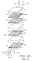
- a conventional example of a laminated dielectric filter is described below. The following explanation relates to a laminated "LC filter” (trade mark) that is put into practical use as a laminated dielectric filter by forming lumped element type capacitors and inductors in a laminate structure.
- Fig. 12 is a perspective exploded view showing the structure of a conventional laminate "LC filter".
- reference numerals 1 and 2 are thick dielectric layers.
- inductor electrodes 3a, 3b, and capacitor electrodes 4a, 4b are formed on a dielectric sheet 4, capacitor electrodes 5a, 5b on a dielectric sheet 5, and shield electrodes 7a, 7b on a dielectric sheet 7.
- the confronting capacitor electrodes 4a and 5a, and 4b and 5b respectively compose parallel plate capacitors.
- Each parallel plate capacitor functions as a resonance circuit as connected in series to the inductor electrodes 3a, 3b through side electrodes 8a, 8b.
- Two inductors are coupled magnetically.
- the side electrode 8b is a grounding electrode, and the side electrode 8c is connected to terminals 3c, 3d connected to the inductor electrode to compose a band pass filter as input and output terminals (for example, Japanese Laid-open Patent No. 3-72706(1991)).
- FIG. 13(a) and (b) shows the structure of a conventional laminated dielectric filter.
- 1/4 wavelength strip lines 820, 821 are formed on a dielectric substrate 819.
- Input and output electrodes 823, 824 are formed on the same plane as the strip lines 820, 821.
- the strip line 820 is composed of a first portion 820a (L 1 indicates the length of 820a) having a first line width W 1 (Z 1 indicates the characteristic impedance of W 1 ) confronting the input and output electrodes 823, a second portion 820b (L 2 indicates the length of 820b) having a second line width narrower than the first line width W 1 , and a third portion 820c having a third line width narrower than the first line width W 1 but broader than the second line width W 2 (Z 2 indicates the characteristic impedance of W 2 ).
- the strip line 821 is composed of a first portion 821a having a first line width W 1 confronting the input and output electrodes 824, a second portion 821b having a second line width narrower than the first line width W 1 , and a third portion 821c having a third line width narrower than the first line width W 1 but broader than the second line width W 2 .
- the strip lines 820, 821 are connected with a short-circuit electrode 822, and the resonator 801b is in a pi-shape.
- a dielectric substrate 819 is covered by grounding electrodes 825, 826 at both surfaces.
- side electrodes 827,828 are formed, and the grounding electrodes 825, 826, and short-circuit electrodes 822 are connected.
- side electrodes to be connected with the input and output electrodes 823, 824 respectively are formed.
- the strip lines 820, 821 are capacitively coupled with the input and output electrodes 823, 824, respectively, thereby constituting a filter as described for example, in U. S. Patent 5,248,949.
- US-4 701 727 discloses a stripline tapped-line filter including a first substrate upon which a plurality of N hairpin resonators are disposed alternately on opposite surfaces of the first substrate. Each one of the hairpin resonators is in a parallel coupled relationship with an adjacent hairpin resonator disposed on an opposite surface of the first substrate. The first and last hairpin resonators each have an interconnected member disposed on the substrate for respectively coupling a signal into and out of the plurality of N hairpin resonators. Second and third substrates are included with each being respectively located adjacent to ones of the plurality of N hairpin resonators on opposite surfaces of the first substrate. First and second groundplanes are included with each respectively located adjacent the second and third substrates.
- An aspect of this invention provides a laminated dielectric antenna duplexer by providing a laminate by laminating and baking integrally a plurality of dielectric sheets, at least three layers or more of shield electrode layers, and at least two layers or more of strip line resonator electrode layers, dividing the laminate into upper and lower laminate parts by at least one layer of shield electrode layer, providing a reception filter in one part of the laminate by at least one layer of strip line resonator electrode layer, providing a transmission filter in another part of the laminate by at least one layer of the strip line resonator electrode layer, and shielding the upper and lower parts of the laminate by using the shield electrode layers, thereby laminating the reception filter and transmission filter in upper and lower layers.
- the laminated dielectric filter antenna duplexer of the embodiment by forming the reception filter and transmission filter into one body in a vertical laminate structure, an antenna duplexer of small size, thin type, and low cost can be attained. By being shielded entirely, moreover, this can be formed as surface mounting device (SMD), and coupling elements of input and output are all formed in the inner layer electrode patterns, so that external parts are not necessary.
- SMD surface mounting device
- the transmission terminal and reception terminal are comprised of side electrodes of different sides.
- the laminated dielectric filter antenna duplexer of the invention as set forth in this embodiment, by forming the : transmission terminal and reception terminal by side electrodes of different sides, sufficient isolation is established between the transmission terminal and reception terminal.
- the strip line resonator electrode layers are comprised of plural front end short-circuit strip line resonators, respectively. and the short-circuit end directions of the strip line resonator to be coupled directly with the transmission terminal and the strip line resonator to be coupled directly with the reception terminal are set in mutually different side directions.
- the capacitive coupling system can be formed through coupling capacitors, and hence the magnetic coupling line that is required in the comb-line filter is not necessary, and both transmission filter and reception filter can be reduced in size.
- the laminate is divided into two upper and lower laminate parts by a separation layer comprised by a plurality of dielectric sheets enclosed in at least two layers of shield electrode layers, and an impedance matching element formed by an electrode pattern on the dielectric sheet of the separation layer.
- a separation layer comprised by a plurality of dielectric sheets enclosed in at least two layers of shield electrode layers, and an impedance matching element formed by an electrode pattern on the dielectric sheet of the separation layer.
- Fig. 1 is a perspective exploded view of a laminated dielectric antenna duplexer in a first embodiment of the invention.
- Fig. 2 is an equivalent circuit diagram of the laminated dielectric antenna duplexer in the first embodiment of the invention.
- Fig. 3 is a perspective exploded view of a laminated dielectric antenna duplexer in a second embodiment of the invention.
- Fig. 4 is an equivalent circuit diagram of the laminated dielectric antenna duplexer in the second embodiment of the invention.
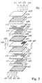
- Fig. 5 is a perspective exploded view of a laminated dielectric antenna duplexer in a third embodiment of the invention.
- Fig. 6 is an equivalent circuit diagram of the laminated dielectric antenna duplexer in the third embodiment of the invention.
- Fig. 7 is a perspective exploded view of a laminated dielectric antenna duplexer in a fourth embodiment of the invention.
- Fig. 8 is a perspective exploded view of a laminated dielectric antenna duplexer in a fifth embodiment of the invention.
- Fig. 9 is a perspective exploded view of a dielectric antenna duplexer of the prior art.
- Fig. 10 is a perspective view of a block dielectric filter of the prior art.
- Fig. 11 is a graph showing transmission characteristic and reflection characteristic of a comb-line dielectric filter of the prior art.
- Fig. 12 is a perspective exploded view of a laminated LC filter of the prior art.
- Fig. 13 (a) and (b) are a perspective view of a laminated dielectric filter of the prior art.
- An antenna duplexer is comprises a combination of a transmission filter and a reception filter.
- FIG. 1 is a perspective exploded view of a laminated dielectric antenna duplexer 500 in the first embodiment of the invention.
- reference numerals 401 through 408 are dielectric sheets
- 411 to 413 and 421 to 423 are strip line resonator electrodes
- 431, 432 and 441, 442 are coupling capacitor electrodes
- 433 and 443 are loading capacitor electrodes
- 451 to 453 are shield electrodes
- 461 is an antenna terminal electrode
- 471 is a transmission terminal electrode
- 481 is a reception terminal electrode
- 462 and 472 to 474, and 482 to 484 are grounding terminal electrodes.
- the dielectric sheets and electrode layers are laminated in the sequence shown in Fig. 1, and are baked integrally.
- Fig. 2 is an equivalent circuit diagram of the laminated dielectric antenna duplexer 500 in the first embodiment of the invention. In thus constituted laminated dielectric antenna duplexer, the operation is described below while referring to Fig. 1 and Fig. 2.
- the strip line resonators 511, 512, 513 composed of the strip line resonator electrodes 411, 412, 413 are resonators composed of front end short-circuit transmission lines shorter than the quarter wavelength, and are formed closely to each other on a dielectric sheet 402.
- the strip line resonators are lowered in resonance frequency by loading capacitor 533, 534, 535 formed between the loading capacitor electrode 433 and strip line resonator electrodes 411, 412, 413, while the adjacent strip line resonators are mutually coupled in electromagnetic field, and a band pass characteristic is shown.
- a coupling capacitor 531 is formed between the coupling electrode 431 and strip line resonator electrode 411, and is electrically connected to an antenna 503 through an antenna terminal 551.
- a coupling capacitor 532 is formed, and is electrically connected to a transmitter 504 through a transmission terminal 552. In this way, a comb-line type transmission filter 501 having a band pass characteristic is formed.
- strip line resonators 521, 522, 523 composed of strip line resonator electrodes 421, 422, 423 are resonators composed of front end short-circuit transmission lines shorter than the quarter wavelength, and are formed closely to each other on a dielectric sheet 405.
- the strip line resonators are lowered in resonance frequency by loading capacitor 543, 544, 545 formed between the loading capacitor electrode 443 and strip line resonator electrodes 421, 422, 423, while the adjacent strip line resonators are mutually coupled in electromagnetic field, and a band pass characteristic is shown.
- a coupling capacitor 541 is formed between the coupling electrode 441 and strip line resonator electrode 421, and is electrically connected to the antenna 503 through the antenna terminal 551.
- a coupling capacitor 542 is formed, and is electrically connected to a receiver 505 through a reception terminal 553. In this way, a comb-line type reception filter 502 having a band pass characteristic is formed.
- the capacity coupling embodiment through coupling capacitors 531, 532, and 541, 542 does not require a coupling line as compared with the magnetic field coupling embodiment generally employed in the comb-line filter, so that both transmission filter and reception filter can be reduced in size.
- One end of the transmission filter 501 is connected to the transmission terminal 552 electrically connected with the transmitter 504, and the other end of the transmission filter 501 is connected to one end of the reception filter 502, and is also connected to the antenna terminal 551 electrically connected to the antenna 503.
- the other end of the reception filter 502 is connected to the reception terminal 553 electrically connected to the receiver 505.
- the transmission filter 501 shows a small insertion loss to the transmission signal in the transmission frequency band which is a passing band, so that the transmission signal can be transmitted from the transmission terminal 552 to the antenna terminal 551 without being attenuated practically.
- the reception signal in the reception frequency band shows a large insertion loss, and the input signal in the reception frequency band is reflected almost completely, and therefore the reception signal entered from the antenna terminal 551 returns to the reception filter 502.
- the reception filter 502 shows a small insertion loss to the reception signal in the reception frequency band, and the reception signal can be transmitted from the antenna terminal 551 to the reception terminal 553 without being attenuated practically.
- the transmission signal in the transmission frequency band shows a large insertion loss, and the input signal in the transmission frequency band is reflected almost completely, and therefore the transmission signal coming from the transmission filter 501 is sent out to the antenna terminal 551.
- the direction of the short-circuit ends of the strip line resonator electrodes 411, 412, 413 for composing the transmission filter 501, and the direction of the short-circuit ends of the strip line resonator electrodes 421, 422, 423 for composing the reception filter 502 are mutually opposite directions.
- the take-out directions of the coupling electrodes 431 and 441 for composing the coupling capacitors 531 and 541 connected to the antenna terminal 551 are set in the same side direction
- the take-out direction of the coupling electrode 442 for composing the coupling capacitor 542 to be connected to the reception terminal 553 may be set on the side of the opposite direction. Therefore, the distance between the transmission terminal electrode 471 and the reception terminal electrode 481 can be extended, so that sufficient isolation may be maintained between the transmission terminal and reception terminal.
- the height of the transmission filter block and the reception filter block is about 2 mm at minimum due to the limit of fine processing of coaxial forming of the ceramic. Therefore, when placed up and down, the total height exceeds 4 mm.
- the thickness of each dielectric sheet is about 30 mm, and the total height can be easily kept within 2 mm.
- input and output coupling elements are composed in inner layer electrode patterns, and external parts are not needed.
- the structure comprising a plurality of dielectric sheets, at least three layers of shield electrode layers, and at least two layers of strip line resonator electrode layers
- the structure is divided into a top and bottom by at least one layer of shield electrode layer.
- the dielectric sheets, shield electrode layers, and strip line resonator electrode layers are laminated and baked into one body to form the reception filter and transmission filter, the reception filter and transmission filter are laminated in upper and lower layers, and therefore a small and thin antenna duplexer of low cost is realized.
- the side of forming the short-circuit end of the front end short-circuit strip line resonator coupled with the reception terminal in the strip line resonator electrode layers for composing the reception filter, and the side for forming the short-circuit end of the front end short-circuit strip line resonator coupled with the transmission terminal in the strip line resonator electrode layers for composing the transmission filter are set in different directions, and the transmission terminal and reception terminal are formed of side electrodes of different sides, so that a sufficient isolation is kept between the transmission terminal and reception terminal.
- the reception filter is laminated on the transmission filter, but, to the contrary, the transmission filter may be laminated on the reception filter, which is similarly applied to the succeeding embodiments.
- FIG. 3 is a perspective exploded view of a laminated dielectric antenna duplexer 554 in the second embodiment of the invention, and those elements corresponding to the elements in Fig. 1 are identified with the same reference numerals.
- Fig. 4 is an equivalent circuit diagram of the laminated dielectric antenna duplexer 554 of the second embodiment, and those elements corresponding to the elements in Fig. 2 are identified with the same reference numerals.
- Fig. 3 differs from Fig. 1 in that the structure is divided into a top and bottom by a separation layer 489 composed by enclosing two dielectric sheets 485, 486 with two layers of shield electrode layers 452, 488, and that an inductor 555 formed of an electrode 487 is added as an impedance matching element on the intermediate dielectric sheet 485 of the separation layer 439.
- a separation layer 489 composed by enclosing two dielectric sheets 485, 486 with two layers of shield electrode layers 452, 488, and that an inductor 555 formed of an electrode 487 is added as an impedance matching element on the intermediate dielectric sheet 485 of the separation layer 439.
- the operation of the thus constituted laminated dielectric antenna duplexer 554 is the same as in the first embodiment except that the inductor 555 is added. As the inductor 555 is inserted between the antenna terminal and the ground, the impedance matching of the antenna 503 with the transmission filter 501 and reception filter 502 is achieved more favorably.
- the structure is divided into a top and bottom by a separation layer enclosing the plurality of dielectric sheets with at least two layers of shield electrode layers, the dielectric sheets, shield electrode layers, and strip line resonator electrode layers are laminated and baked into one body to compose reception filter and transmission filter, the reception filter and transmission filter are laminated in upper and lower layers, and moreover an inductor is formed as impedance matching element on the intermediate dielectric sheet of the separation layer, so that a favorable matching characteristic may be realized, aside from the same effects as in the first embodiment.
- FIG. 5 is a perspective exploded view of a laminated dielectric antenna duplexer 556 showing the third embodiment of the invention, and those elements corresponding to the elements in Fig. 1 and Fig. 3 are identified with the same reference numerals.
- Fig. 6 is an equivalent circuit diagram of the laminated dielectric antenna duplexer 556 in the third embodiment. Those elements corresponding to the elements in Fig. 2 and Fig. 4 are identified with the same reference numerals.
- Fig. 5 differs from Fig. 3 in that the structure is divided into a top and bottom by a separation layer 496 composed by holding three dielectric sheets 490, 491, 492 with two shield electrode layers 452, 495, and that a capacitor 557 formed of electrodes 493, 494 is added as impedance matching element on the intermediate dielectric sheets 499, 491 of the separation layer 496.
- a separation layer 496 composed by holding three dielectric sheets 490, 491, 492 with two shield electrode layers 452, 495, and that a capacitor 557 formed of electrodes 493, 494 is added as impedance matching element on the intermediate dielectric sheets 499, 491 of the separation layer 496.
- the operation of the thus constituted laminated dielectric antenna duplexer 554 is the same as in the first embodiment except that the capacitor 557 is added. As the capacitor 557 is inserted between the antenna terminal and the ground, the impedance matching of the antenna 503 with the transmission filter 501 and reception filter 502 is achieved more favorably.
- the structure is divided into a top and bottom by a separation layer enclosing the plurality of dielectric sheets with at least two layers of shield electrode layers, the dielectric sheets, shield electrode layers, and strip line resonator electrode layers are laminated and baked into one body to compose reception filter and transmission filter, the reception filter and transmission filter are laminated in upper and lower layers, and moreover a capacitor is formed as impedance matching element on the intermediate dielectric sheet of the separation layer, so that the same effects as in the first embodiment and second embodiment may be achieved.
- the transmission filters and reception filters are comb-line type band pass filters for coupling the strip line resonators in the electromagnetic field, but band pass filters of other type than comb-line type for coupling with inductor or capacitor may be used, or band elimination filter or low pass filter may be also used.
- band pass filters of other type than comb-line type for coupling with inductor or capacitor may be used, or band elimination filter or low pass filter may be also used.
- FIG. 7 is a perspective exploded view of the laminated dielectric antenna duplexer showing the fourth embodiment of the invention.
- strip line resonator electrodes 611a to 611f are formed on a dielectric sheet 600a and a dielectric sheet 600f, and each consists of broad parts 612a to 612f, and narrow parts 613a to 613f.
- the short-circuit end side of the narrow parts is connected and grounded to side electrodes 605a to 605f as grounding terminals, through broad common grounding electrodes 616a, 616b.
- Electric field coupling between adjacent strip line resonators is achieved through second electrodes 641a, 642a formed on the dielectric sheet 600c, and second electrodes 641b, 642b formed on the dielectric sheet 600h.
- the adjacent strip line resonators are mutually coupled in electromagnetic field, and is coupled in electric field through interstage coupling capacitor, and coupling of strip line resonators is achieved by the combination of electromagnetic field coupling and electric field coupling.
- an attenuation pole may be constituted in the transmission characteristic.
- third electrodes 643a, 643b are partly formed and grounded in the remaining regions of forming the second electrodes.
- Parallel flat plate capacitors composed between the third electrodes and strip line resonator electrodes function as parallel loading capacitors for lowering the resonance frequency of the strip line resonator. Therefore, the length of the strip line resonator may be set shorter than the quarter wavelength, so that the filter may be reduced in size.
- Fourth electrodes 602a to 602d formed in the region contacting the strip line resonator electrode on the dielectric sheets 600c, 600h compose an input and output coupling capacitor together with the strip line resonator electrode.
- the fourth electrode 602a is connected to a side electrode 604b as a reception terminal
- the fourth electrode 602c is connected to a side electrode 604c as a transmission terminal
- the fourth electrodes 602b, 602d are connected to a side electrode 604a as an antenna terminal.
- the structure is divided into a top and bottom by a separation layer constituted by enclosing two dielectric sheets 600j, 600d by two layers of shield electrode layers 644b, 644c, and an inductor is formed by an electrode 617 as an impedance matching element on the dielectric sheet 600j.
- Shield electrodes 644a, 644d are formed to cover the whole surface on the dielectric sheets 600b, 600i.
- the upper shield electrode layer 644a made of inner layer electrode not sufficient in mechanical strength is protected.
- the shield electrodes 644a to 644d are connected and grounded to the side electrodes 605a to 605g.
- a reception filter is composed of dielectric sheets 600a to 600e and electrodes formed thereon, and a transmission filter is composed of dielectric sheets 600f to 600i and electrodes formed thereon.
- the inductor composed of the electrode 617 formed on the dielectric sheet 600j is inserted between the antenna terminal and ground, the impedance matching of the antenna with the transmission filter and reception filter may be achieved favorably.
- the laminated dielectric antenna duplexer of the embodiment has the same effects as in the second embodiment, an attenuation pole is formed in the transmission characteristic, and excellent selectivity is achieved.
- FIG. 8 is a perspective exploded view of the laminated dielectric antenna duplexer of the fifth embodiment of the invention.
- strip line resonator electrodes 651a to 651f are formed on dielectric sheets 650c, 650e, 650g, and dielectric sheets 650g, 650q, 650s, and each one is composed of broad parts 652a to 652f, and narrow parts 653a to 653f.
- the short-circuit end side of the narrow parts is connected and grounded to side electrodes 658c to 658e as grounding terminals through broad grounding electrodes 654a to 654f.
- input and output coupling capacity electrodes 655a to 655d confronting the strip line resonator electrodes are formed on the dielectric sheets 650b, 650h, 650m, 650t.
- the input and output coupling capacity electrode 655d is connected to the side electrode 657c as reception terminal
- the input and output coupling capacity electrode 655a is connected to the side electrode 657b as a transmission terminal
- the input and output coupling capacity electrodes 655b, 655c are connected to the side electrode 657a as an antenna terminal.
- loading capacitor electrodes 659a, 650d are formed in the region contacting the strip line resonator electrodes on the dielectric sheets 650d, 650f, 650p, 650r.
- the loading capacitor electrodes 659a, 650d are connected and grounded to the side electrodes 658a, 658b. These capacitors function to lower the resonance frequency of the strip line resonator. Therefore, the length of the strip line resonator can be cut further shorter than the shortening by the SIR structure, so that the filter may be further reduced in size.
- the electromagnetic field coupling amounts of the first transmission lines and second transmission lines are independently set, and a passing band and attenuation pole are generated in the transmission characteristic.
- the strip line resonator electrodes 651a, 651f are laminated up and down by aligning the direction of the grounding ends, and the broad parts 652a to 652f, and narrow parts 653a to 653f are mutually coupled in electromagnetic field.
- the electromagnetic field coupling amount of the strip lines is adjusted by shifting the strip line position in the vertical direction. By shifting the line center lines of the broad parts and narrow parts of the strip lines from the same line, the electromagnetic field coupling of the broad parts of the strip lines, and the electromagnetic field coupling of the narrow parts can be set independently. By thus setting the coupling amount independently, it is possible to design to form an attenuation pole at a desired frequency.
- independent electromagnetic field coupling of the open end side broad parts and grounding end side narrow parts not only the band passing characteristic is shown in the passing region, but also an attenuation pole may be formed at a desired frequency of transmission characteristic. Therefore, a selectivity characteristic superior to Chebyshev characteristic may are obtained.
- the structure is divided into a top and bottom by a separation layer constituted by enclosing two dielectric sheets 650j, 650d by two layers of shield electrode layers 656b, 656c, and a inductor is formed by an electrode 660 as an impedance matching element on the dielectric sheet 650j.
- Shield electrodes 656a, 656d are formed to cover the whole surface on the dielectric sheets 650a, 650u.
- the upper shield electrode layer 656d made of inner layer electrode not sufficient in mechanical strength is protected.
- the shield electrodes 656a to 656d are connected and grounded to the side electrodes 658a to 658i.
- a reception filter is composed of dielectric sheets 650k to 650v and electrodes formed thereon, and a transmission filter is composed of dielectric sheets 650a to 650i and electrodes formed thereon.
- the inductor composed of the electrode 660 formed on the dielectric sheet 650j is inserted between the antenna terminal and ground, the impedance matching of the antenna with the transmission filter and reception filter may be achieved favorably.
- the laminated dielectric antenna duplexer of the embodiment has the same effects as in the second embodiment, an attenuation pole is formed in the transmission characteristic, and an excellent selectivity may be realized.
Description
- This invention relates to a dielectric antenna duplexer used mainly in high frequency radio devices such as mobile telephones. An antenna duplexer is a device for sharing one antenna by a transmitter and a receiver, and it is composed of a transmission filter and a reception filter. The invention is particularly directed to a laminated dielectric antenna duplexer having a laminate structure by laminating a dielectric sheet and an electrode layer and baking into one body.
- Along with the advancement of mobile communications, recently, the antenna duplexer is used widely in many hand-held telephones and car-mounted telephones. An example of a conventional antenna duplexer is described below with reference to a drawing.
- Fig. 9 is a perspective exploded view of a conventional antenna duplexer. In Fig. 9,
reference numerals 701 to 706 are dielectric coaxial resonators, 707 is a coupling substrate, 708 is a metallic case, 709 is a metallic cover, 710 to 712 are series capacitors, 713 and 714 are inductors, 715 to 718 are coupling capacitors, 721 to 726 are coupling pins, 731 is a transmission terminal, 732 is an antenna terminal, 733 is a reception terminal, and 741 to 747 are electrode patterns formed on thecoupling substrate 707. - The dielectric
coaxial resonators series capacitors coaxial resonators coupling capacitors 715, 716, 717, 718 compose a reception band pass filter. - One end of the transmission filter is connected to a transmission terminal which is electrically connected with a transmitter, and the other end of the transmission filter is connected to one end of a reception filter, and is also connected to an antenna terminal electrically connected to the antenna. The other end of the reception filter is connected to a reception terminal which is electrically connected to a receiver.
- The operation of an antenna duplexer is described below. First of all, the transmission band elimination filter shows a small insertion loss to the transmission signal in the transmission frequency band, and can transmit the transmission signal from the transmission terminal to the antenna terminal while hardly attenuating it. By contrast, it shows a larger insertion loss to the reception signal in the reception frequency band, and reflects almost all input signal in the reception frequency band, and therefore the reception signal entering from the antenna terminal returns to the reception band pass filter.
- On the other hand, the reception band filter shows a small insertion loss to the reception signal in the reception frequency band, and transmits the reception signal from the antenna terminal to the reception terminal while hardly attenuating it. The transmission signal in the transmission frequency band shows a large insertion loss, and reflects almost all input signal in the transmission frequency band, so that the transmission signals coming from the transmission filter is sent out to the antenna terminal.
- In this design, however, in manufacturing dielectric coaxial resonators, there is a limitation in fine processing of ceramics, and hence it is hard to reduce its size. Downsizing is also difficult because many parts are used such as capacitors and inductors, and another problem is the difficulty in lowering the assembling cost.
- The dielectric filter is a constituent element of the antenna duplexer, and is also used widely as an independent filter in mobile telephones and radio devices, and there is a demand that they be smaller in size and higher in performance. Referring now to a different drawing, an example of a conventional block type dielectric filter possessing a different constitution from the above described structure is described below.
- Fig. 10 is a perspective oblique view of a block type dielectric filter of the prior art. In Fig. 10,
reference numeral 1200 is a dielectric block, 1201 to 1204 are penetration holes, and 1211 to 1214, and 1221, 1222, 1230 are electrodes. Thedielectric block 1200 is entirely covered with electrodes, including the surface of the penetration holes 1201 to 1204, except for peripheral parts of the electrodes on the surface of which theelectrodes 1221, 1222 and others are formed. - The operation of the thus constituted dielectric filter is described below. The surface electrodes in the penetration holes 1201 to 1204 serve as the resonator, and the
electrode 1230 serves as the shield electrode. Theelectrodes 1211 to 1214 are to lower the resonance frequency of the resonator composed of the electrodes in the penetration holes, and functions as the loading capacity electrode. By nature, a 1/4 wavelength front end short-circuit transmission line is not coupled at the resonance frequency and shows a band stop characteristic, but by thus lowering the resonance frequency, an electromagnetic field coupling between transmission lines occurs in the filter passing band, so that a band pass filter is created. Theelectrodes 1221, 1222 are input and output coupling capacity electrodes, and input and output coupling is effected by the capacity between these electrodes and the resonator, and the loading capacity electrode. - The operating principle of this filter is a modified version of a comb-line filter disclosed in the literature (for example, G.L. Matthaei, "Comb-Line Band-pass Filters of Narrow or Moderate Bandwidth"; the Microwave Journal, August 1963). The block type filter in this design is a comb-line filter composed of a dielectric ceramic (for example, see U. S. Patent 4,431,977). The comb-line filter always requires a loading capacity for lowering the resonance frequency in order to realize the band pass characteristic.
- Fig. 11 shows the transmission characteristic of the comb-line type dielectric filter in the prior art. The transmission characteristic shows the Chebyshev characteristic increasing steadily as the attenuation outside the bandwidth departs from the center frequency.
- In this construction, however, it is not possible to realize the elliptical function characteristic possessing the attenuation pole near the bandwidth of the transmission characteristic, and hence the range of selection is not sufficient for filter performance.
- Also, in such dielectric filter, for smaller and thinner constitution, the flat type laminate dielectric filter that can be made thinner than the coaxial type is expected henceforth, and several attempts have been made to design such a device. A conventional example of a laminated dielectric filter is described below. The following explanation relates to a laminated "LC filter" (trade mark) that is put into practical use as a laminated dielectric filter by forming lumped element type capacitors and inductors in a laminate structure.
- Fig. 12 is a perspective exploded view showing the structure of a conventional laminate "LC filter". In Fig. 12,
reference numerals 1 and 2 are thick dielectric layers. On adielectric sheet 3 are formedinductor electrodes capacitor electrodes capacitor electrodes dielectric sheet 5, andshield electrodes dielectric sheet 7. By stacking up all these dielectric layers and dielectric sheets together with adielectric sheet 6 for protecting the electrodes, an entirely laminated structure is formed. - The operation of the thus constituted dielectric filter is described below. First, the confronting
capacitor electrodes inductor electrodes side electrodes side electrode 8b is a grounding electrode, and theside electrode 8c is connected toterminals 3c, 3d connected to the inductor electrode to compose a band pass filter as input and output terminals (for example, Japanese Laid-open Patent No. 3-72706(1991)). - In such a constitution, however, when the inductor electrodes are brought closer to each other to narrow the interval in order to reduce in its size, the magnetic field coupling between the resonators becomes too large, and it is hard to realize a favorable band pass characteristic narrow in the bandwidth. It is moreover difficult to heighten the unloaded Q value of the inductor electrodes, and hence the filter insertion loss is large.
- Another different conventional example of a laminated dielectric filter is described below with reference to an accompanying drawing. Fig. 13(a) and (b) shows the structure of a conventional laminated dielectric filter. In Fig. 13(a) and (b), 1/4
wavelength strip lines dielectric substrate 819. Input andoutput electrodes strip lines strip line 820 is composed of a first portion 820a (L1 indicates the length of 820a) having a first line width W1 (Z1 indicates the characteristic impedance of W1) confronting the input andoutput electrodes 823, a second portion 820b (L2 indicates the length of 820b) having a second line width narrower than the first line width W1, and athird portion 820c having a third line width narrower than the first line width W1 but broader than the second line width W2 (Z2 indicates the characteristic impedance of W2). Similarly, thestrip line 821 is composed of afirst portion 821a having a first line width W1 confronting the input andoutput electrodes 824, asecond portion 821b having a second line width narrower than the first line width W1, and a third portion 821c having a third line width narrower than the first line width W1 but broader than the second line width W2. Thestrip lines circuit electrode 822, and the resonator 801b is in a pi-shape. Adielectric substrate 819 is covered bygrounding electrodes grounding electrodes circuit electrodes 822 are connected. On theother side 819b, side electrodes to be connected with the input andoutput electrodes strip lines output electrodes - In such constitution, however, same as the conventional block type dielectric filter, the elliptical function characteristic possessing the attenuation pole near the passing band of the transmission characteristic cannot be realized. and hence the scope of performance of the filter is not wide enough.
- US-4 701 727 discloses a stripline tapped-line filter including a first substrate upon which a plurality of N hairpin resonators are disposed alternately on opposite surfaces of the first substrate. Each one of the hairpin resonators is in a parallel coupled relationship with an adjacent hairpin resonator disposed on an opposite surface of the first substrate. The first and last hairpin resonators each have an interconnected member disposed on the substrate for respectively coupling a signal into and out of the plurality of N hairpin resonators. Second and third substrates are included with each being respectively located adjacent to ones of the plurality of N hairpin resonators on opposite surfaces of the first substrate. First and second groundplanes are included with each respectively located adjacent the second and third substrates.
- Jpn. J. Appl. Phys. Vol. 31 (1992) pp. 3152-3155 discloses that resonant devices of band-pass filters and antenna duplexers can be miniaturized by multilayer microwave devices.
- IEEE Transactions on Microwave Theory and Techniques 41 (1993) February, No. 2 pp. 215-223 relates to quasi-planar realizations of combline bandpass filters and diplexers using multiple coupled suspended substrate striplines. In its Fig. 2 a three-dimensional view of a combline diplexer configuration with the top cover taken off is shown.
- It is a primary object of the invention to provide an antenna duplexer at low cost which has an excellent band pass characteristic with small insection loss and high bandwidth selectivity. Another object is to provide a laminated dielectric antenna duplexer and laminate dielectric filters having a small and thin flat structure.
- The objects are achieved by the features of the claims.
- An aspect of this invention provides a laminated dielectric antenna duplexer by providing a laminate by laminating and baking integrally a plurality of dielectric sheets, at least three layers or more of shield electrode layers, and at least two layers or more of strip line resonator electrode layers, dividing the laminate into upper and lower laminate parts by at least one layer of shield electrode layer, providing a reception filter in one part of the laminate by at least one layer of strip line resonator electrode layer, providing a transmission filter in another part of the laminate by at least one layer of the strip line resonator electrode layer, and shielding the upper and lower parts of the laminate by using the shield electrode layers, thereby laminating the reception filter and transmission filter in upper and lower layers. In the laminated dielectric filter antenna duplexer of the embodiment, by forming the reception filter and transmission filter into one body in a vertical laminate structure, an antenna duplexer of small size, thin type, and low cost can be attained. By being shielded entirely, moreover, this can be formed as surface mounting device (SMD), and coupling elements of input and output are all formed in the inner layer electrode patterns, so that external parts are not necessary.
- It is preferable that the transmission terminal and reception terminal are comprised of side electrodes of different sides. In the laminated dielectric filter antenna duplexer of the invention as set forth in this embodiment, by forming the : transmission terminal and reception terminal by side electrodes of different sides, sufficient isolation is established between the transmission terminal and reception terminal.
- It is preferable that the strip line resonator electrode layers are comprised of plural front end short-circuit strip line resonators, respectively. and the short-circuit end directions of the strip line resonator to be coupled directly with the transmission terminal and the strip line resonator to be coupled directly with the reception terminal are set in mutually different side directions. The capacitive coupling system can be formed through coupling capacitors, and hence the magnetic coupling line that is required in the comb-line filter is not necessary, and both transmission filter and reception filter can be reduced in size.
- It is preferable that the laminate is divided into two upper and lower laminate parts by a separation layer comprised by a plurality of dielectric sheets enclosed in at least two layers of shield electrode layers, and an impedance matching element formed by an electrode pattern on the dielectric sheet of the separation layer. In the laminated dielectric filter antenna duplexer of this embodiment. by forming an inductor cr capacitor as an impedance matching element on the dielectric sheet between separation layers, a favorable matching characteristic between the antenna terminals between the transmission filter and reception filter can be realized.
- Fig. 1 is a perspective exploded view of a laminated dielectric antenna duplexer in a first embodiment of the invention.
- Fig. 2 is an equivalent circuit diagram of the laminated dielectric antenna duplexer in the first embodiment of the invention.
- Fig. 3 is a perspective exploded view of a laminated dielectric antenna duplexer in a second embodiment of the invention.
- Fig. 4 is an equivalent circuit diagram of the laminated dielectric antenna duplexer in the second embodiment of the invention.
- Fig. 5 is a perspective exploded view of a laminated dielectric antenna duplexer in a third embodiment of the invention.
- Fig. 6 is an equivalent circuit diagram of the laminated dielectric antenna duplexer in the third embodiment of the invention.
- Fig. 7 is a perspective exploded view of a laminated dielectric antenna duplexer in a fourth embodiment of the invention.
- Fig. 8 is a perspective exploded view of a laminated dielectric antenna duplexer in a fifth embodiment of the invention.
- Fig. 9 is a perspective exploded view of a dielectric antenna duplexer of the prior art.
- Fig. 10 is a perspective view of a block dielectric filter of the prior art.
- Fig. 11 is a graph showing transmission characteristic and reflection characteristic of a comb-line dielectric filter of the prior art.
- Fig. 12 is a perspective exploded view of a laminated LC filter of the prior art.
- Fig. 13 (a) and (b) are a perspective view of a laminated dielectric filter of the prior art.
- An antenna duplexer is comprises a combination of a transmission filter and a reception filter.
- A laminated dielectric antenna duplexer in a first embodiment of the invention is described with reference to drawings. Fig. 1 is a perspective exploded view of a laminated
dielectric antenna duplexer 500 in the first embodiment of the invention. In Fig. 1,reference numerals 401 through 408 are dielectric sheets, 411 to 413 and 421 to 423 are strip line resonator electrodes, 431, 432 and 441, 442 are coupling capacitor electrodes, 433 and 443 are loading capacitor electrodes, 451 to 453 are shield electrodes, 461 is an antenna terminal electrode, 471 is a transmission terminal electrode, 481 is a reception terminal electrode, and 462 and 472 to 474, and 482 to 484 are grounding terminal electrodes. The dielectric sheets and electrode layers are laminated in the sequence shown in Fig. 1, and are baked integrally. - Fig. 2 is an equivalent circuit diagram of the laminated
dielectric antenna duplexer 500 in the first embodiment of the invention. In thus constituted laminated dielectric antenna duplexer, the operation is described below while referring to Fig. 1 and Fig. 2. - The
strip line resonators line resonator electrodes dielectric sheet 402. The strip line resonators are lowered in resonance frequency by loadingcapacitor loading capacitor electrode 433 and stripline resonator electrodes coupling capacitor 531 is formed between thecoupling electrode 431 and stripline resonator electrode 411, and is electrically connected to anantenna 503 through anantenna terminal 551. Likewise, between thecoupling electrode 432 and stripline resonator electrode 413, acoupling capacitor 532 is formed, and is electrically connected to atransmitter 504 through atransmission terminal 552. In this way, a comb-linetype transmission filter 501 having a band pass characteristic is formed. - On the other hand,
strip line resonators line resonator electrodes dielectric sheet 405. The strip line resonators are lowered in resonance frequency by loadingcapacitor loading capacitor electrode 443 and stripline resonator electrodes coupling capacitor 541 is formed between thecoupling electrode 441 and stripline resonator electrode 421, and is electrically connected to theantenna 503 through theantenna terminal 551. Likewise, between thecoupling electrode 442 and stripline resonator electrode 423, acoupling capacitor 542 is formed, and is electrically connected to areceiver 505 through areception terminal 553. In this way, a comb-linetype reception filter 502 having a band pass characteristic is formed. - The capacity coupling embodiment through
coupling capacitors - One end of the
transmission filter 501 is connected to thetransmission terminal 552 electrically connected with thetransmitter 504, and the other end of thetransmission filter 501 is connected to one end of thereception filter 502, and is also connected to theantenna terminal 551 electrically connected to theantenna 503. The other end of thereception filter 502 is connected to thereception terminal 553 electrically connected to thereceiver 505. - The
transmission filter 501 shows a small insertion loss to the transmission signal in the transmission frequency band which is a passing band, so that the transmission signal can be transmitted from thetransmission terminal 552 to theantenna terminal 551 without being attenuated practically. The reception signal in the reception frequency band shows a large insertion loss, and the input signal in the reception frequency band is reflected almost completely, and therefore the reception signal entered from theantenna terminal 551 returns to thereception filter 502. - The
reception filter 502 shows a small insertion loss to the reception signal in the reception frequency band, and the reception signal can be transmitted from theantenna terminal 551 to thereception terminal 553 without being attenuated practically. The transmission signal in the transmission frequency band shows a large insertion loss, and the input signal in the transmission frequency band is reflected almost completely, and therefore the transmission signal coming from thetransmission filter 501 is sent out to theantenna terminal 551. - In the first embodiment shown in Fig. 1, the direction of the short-circuit ends of the strip
line resonator electrodes transmission filter 501, and the direction of the short-circuit ends of the stripline resonator electrodes reception filter 502 are mutually opposite directions. Accordingly, when the take-out directions of thecoupling electrodes coupling capacitors antenna terminal 551 are set in the same side direction, the take-out direction of thecoupling electrode 432 for composing thecoupling capacitor 532 connected to thetransmission terminal 552, and the take-out direction of thecoupling electrode 442 for composing thecoupling capacitor 542 to be connected to thereception terminal 553 may be set on the side of the opposite direction. Therefore, the distance between thetransmission terminal electrode 471 and thereception terminal electrode 481 can be extended, so that sufficient isolation may be maintained between the transmission terminal and reception terminal. - The construction in the prior art by merely adhering up and down the transmission filter block and reception filter block of the antenna duplexer is compared with the laminated dielectric antenna duplexer conforming to the constitution of the invention.
- First, in the prior art, the height of the transmission filter block and the reception filter block is about 2 mm at minimum due to the limit of fine processing of coaxial forming of the ceramic. Therefore, when placed up and down, the total height exceeds 4 mm. In the constitution of the invention, by contrast, the thickness of each dielectric sheet is about 30 mm, and the total height can be easily kept within 2 mm.
- In the conventional example, for taking out and connecting the terminals, it is required to lay around outside of the filter block by using external parts, and a shield case for shielding the entire structure is needed, but in the constitution of the invention, for terminal connection, patterns of inner layer electrodes are connected to the side electrodes, and the entire structure can be shielded to compose a surface mounted device (SMD).
- In the constitution of the invention, input and output coupling elements are composed in inner layer electrode patterns, and external parts are not needed.
- Thus, according to the embodiment, comprising a plurality of dielectric sheets, at least three layers of shield electrode layers, and at least two layers of strip line resonator electrode layers, the structure is divided into a top and bottom by at least one layer of shield electrode layer. The dielectric sheets, shield electrode layers, and strip line resonator electrode layers are laminated and baked into one body to form the reception filter and transmission filter, the reception filter and transmission filter are laminated in upper and lower layers, and therefore a small and thin antenna duplexer of low cost is realized.
- The side of forming the short-circuit end of the front end short-circuit strip line resonator coupled with the reception terminal in the strip line resonator electrode layers for composing the reception filter, and the side for forming the short-circuit end of the front end short-circuit strip line resonator coupled with the transmission terminal in the strip line resonator electrode layers for composing the transmission filter are set in different directions, and the transmission terminal and reception terminal are formed of side electrodes of different sides, so that a sufficient isolation is kept between the transmission terminal and reception terminal.
- In the embodiment, the reception filter is laminated on the transmission filter, but, to the contrary, the transmission filter may be laminated on the reception filter, which is similarly applied to the succeeding embodiments.
- A laminated dielectric antenna duplexer in a second embodiment of the invention is described while referring to drawings. Fig. 3 is a perspective exploded view of a laminated
dielectric antenna duplexer 554 in the second embodiment of the invention, and those elements corresponding to the elements in Fig. 1 are identified with the same reference numerals. Fig. 4 is an equivalent circuit diagram of the laminateddielectric antenna duplexer 554 of the second embodiment, and those elements corresponding to the elements in Fig. 2 are identified with the same reference numerals. - Fig. 3 differs from Fig. 1 in that the structure is divided into a top and bottom by a
separation layer 489 composed by enclosing twodielectric sheets inductor 555 formed of anelectrode 487 is added as an impedance matching element on theintermediate dielectric sheet 485 of the separation layer 439. - The operation of the thus constituted laminated
dielectric antenna duplexer 554 is the same as in the first embodiment except that theinductor 555 is added. As theinductor 555 is inserted between the antenna terminal and the ground, the impedance matching of theantenna 503 with thetransmission filter 501 andreception filter 502 is achieved more favorably. - Thus, by comprising a plurality of dielectric sheets, at least four layers of shield electrode layers, and at least two layers of strip line resonator electrode layers, the structure is divided into a top and bottom by a separation layer enclosing the plurality of dielectric sheets with at least two layers of shield electrode layers, the dielectric sheets, shield electrode layers, and strip line resonator electrode layers are laminated and baked into one body to compose reception filter and transmission filter, the reception filter and transmission filter are laminated in upper and lower layers, and moreover an inductor is formed as impedance matching element on the intermediate dielectric sheet of the separation layer, so that a favorable matching characteristic may be realized, aside from the same effects as in the first embodiment.
- A laminated dielectric antenna duplexer in a third embodiment of the invention is described below. Fig. 5 is a perspective exploded view of a laminated
dielectric antenna duplexer 556 showing the third embodiment of the invention, and those elements corresponding to the elements in Fig. 1 and Fig. 3 are identified with the same reference numerals. Fig. 6 is an equivalent circuit diagram of the laminateddielectric antenna duplexer 556 in the third embodiment. Those elements corresponding to the elements in Fig. 2 and Fig. 4 are identified with the same reference numerals. - Fig. 5 differs from Fig. 3 in that the structure is divided into a top and bottom by a
separation layer 496 composed by holding threedielectric sheets capacitor 557 formed ofelectrodes intermediate dielectric sheets 499, 491 of theseparation layer 496. - The operation of the thus constituted laminated
dielectric antenna duplexer 554 is the same as in the first embodiment except that thecapacitor 557 is added. As thecapacitor 557 is inserted between the antenna terminal and the ground, the impedance matching of theantenna 503 with thetransmission filter 501 andreception filter 502 is achieved more favorably. - Thus, by comprising a plurality of dielectric sheets, at least four layers of shield electrode layers, and at least two layers of strip line resonator electrode layers, the structure is divided into a top and bottom by a separation layer enclosing the plurality of dielectric sheets with at least two layers of shield electrode layers, the dielectric sheets, shield electrode layers, and strip line resonator electrode layers are laminated and baked into one body to compose reception filter and transmission filter, the reception filter and transmission filter are laminated in upper and lower layers, and moreover a capacitor is formed as impedance matching element on the intermediate dielectric sheet of the separation layer, so that the same effects as in the first embodiment and second embodiment may be achieved.
- In the laminated dielectric antenna duplexers in the first to third embodiments, the transmission filters and reception filters are comb-line type band pass filters for coupling the strip line resonators in the electromagnetic field, but band pass filters of other type than comb-line type for coupling with inductor or capacitor may be used, or band elimination filter or low pass filter may be also used. Various modifications of the transmission filter and reception filter are evident, and are included in the scope of the invention. Embodiments employing such modifications.
- A laminated dielectric antenna duplexer in an fourth embodiment of the invention is described below. Fig. 7 is a perspective exploded view of the laminated dielectric antenna duplexer showing the fourth embodiment of the invention.
- In the constitution of the transmission filter and reception filter, strip
line resonator electrodes 611a to 611f are formed on adielectric sheet 600a and adielectric sheet 600f, and each consists ofbroad parts 612a to 612f, andnarrow parts 613a to 613f. The short-circuit end side of the narrow parts is connected and grounded toside electrodes 605a to 605f as grounding terminals, through broadcommon grounding electrodes 616a, 616b. - Electric field coupling between adjacent strip line resonators is achieved through
second electrodes dielectric sheet 600c, andsecond electrodes dielectric sheet 600h. The adjacent strip line resonators are mutually coupled in electromagnetic field, and is coupled in electric field through interstage coupling capacitor, and coupling of strip line resonators is achieved by the combination of electromagnetic field coupling and electric field coupling. As a result, by the resonance phenomenon due to combination of electromagnetic field coupling and electric field coupling, an attenuation pole may be constituted in the transmission characteristic. - In the regions contacting the strip line resonator electrodes on the
dielectric sheets third electrodes - Fourth electrodes 602a to 602d formed in the region contacting the strip line resonator electrode on the
dielectric sheets fourth electrode 602c is connected to a side electrode 604c as a transmission terminal, and thefourth electrodes side electrode 604a as an antenna terminal. - In the constitution of the laminated dielectric antenna duplexer of the embodiment, the structure is divided into a top and bottom by a separation layer constituted by enclosing two
dielectric sheets electrode 617 as an impedance matching element on thedielectric sheet 600j.Shield electrodes 644a, 644d are formed to cover the whole surface on thedielectric sheets protective dielectric sheet 600e, the uppershield electrode layer 644a made of inner layer electrode not sufficient in mechanical strength is protected. Theshield electrodes 644a to 644d are connected and grounded to theside electrodes 605a to 605g. - A reception filter is composed of
dielectric sheets 600a to 600e and electrodes formed thereon, and a transmission filter is composed ofdielectric sheets 600f to 600i and electrodes formed thereon. As the inductor composed of theelectrode 617 formed on thedielectric sheet 600j is inserted between the antenna terminal and ground, the impedance matching of the antenna with the transmission filter and reception filter may be achieved favorably. - Thus, the laminated dielectric antenna duplexer of the embodiment has the same effects as in the second embodiment, an attenuation pole is formed in the transmission characteristic, and excellent selectivity is achieved.
- A laminated dielectric antenna duplexer in a fifth embodiment of the invention is described below. Fig. 8 is a perspective exploded view of the laminated dielectric antenna duplexer of the fifth embodiment of the invention.
- In the constitution of the transmission filter and reception filter, strip
line resonator electrodes 651a to 651f are formed ondielectric sheets dielectric sheets broad parts 652a to 652f, andnarrow parts 653a to 653f. The short-circuit end side of the narrow parts is connected and grounded toside electrodes 658c to 658e as grounding terminals throughbroad grounding electrodes 654a to 654f. - On the
dielectric sheets coupling capacity electrodes 655a to 655d confronting the strip line resonator electrodes are formed. The input and outputcoupling capacity electrode 655d is connected to theside electrode 657c as reception terminal, the input and outputcoupling capacity electrode 655a is connected to theside electrode 657b as a transmission terminal, and the input and outputcoupling capacity electrodes 655b, 655c are connected to theside electrode 657a as an antenna terminal. - In the region contacting the strip line resonator electrodes on the
dielectric sheets loading capacitor electrodes loading capacitor electrodes side electrodes - In the transmission filter and reception filter of the embodiment, in SIR structure, the electromagnetic field coupling amounts of the first transmission lines and second transmission lines are independently set, and a passing band and attenuation pole are generated in the transmission characteristic. The strip
line resonator electrodes broad parts 652a to 652f, andnarrow parts 653a to 653f are mutually coupled in electromagnetic field. - The electromagnetic field coupling amount of the strip lines is adjusted by shifting the strip line position in the vertical direction. By shifting the line center lines of the broad parts and narrow parts of the strip lines from the same line, the electromagnetic field coupling of the broad parts of the strip lines, and the electromagnetic field coupling of the narrow parts can be set independently. By thus setting the coupling amount independently, it is possible to design to form an attenuation pole at a desired frequency. By independent electromagnetic field coupling of the open end side broad parts and grounding end side narrow parts, not only the band passing characteristic is shown in the passing region, but also an attenuation pole may be formed at a desired frequency of transmission characteristic. Therefore, a selectivity characteristic superior to Chebyshev characteristic may are obtained.
- In the constitution of the laminated dielectric antenna duplexer in the embodiment, the structure is divided into a top and bottom by a separation layer constituted by enclosing two
dielectric sheets electrode 660 as an impedance matching element on thedielectric sheet 650j.Shield electrodes 656a, 656d are formed to cover the whole surface on thedielectric sheets protective dielectric sheet 650v, the uppershield electrode layer 656d made of inner layer electrode not sufficient in mechanical strength is protected. The shield electrodes 656a to 656d are connected and grounded to theside electrodes 658a to 658i. - A reception filter is composed of
dielectric sheets 650k to 650v and electrodes formed thereon, and a transmission filter is composed ofdielectric sheets 650a to 650i and electrodes formed thereon. As the inductor composed of theelectrode 660 formed on thedielectric sheet 650j is inserted between the antenna terminal and ground, the impedance matching of the antenna with the transmission filter and reception filter may be achieved favorably. - Thus, the laminated dielectric antenna duplexer of the embodiment has the same effects as in the second embodiment, an attenuation pole is formed in the transmission characteristic, and an excellent selectivity may be realized.
Claims (4)
- A laminated dielectric antenna duplexer comprising a laminate formed by a plurality of dielectric sheets (401...408), at least three layers of shield electrode layers (451...453), and at least two layers of strip line resonator electrode layers, wherein the laminate is divided in upper and lower laminate parts by at least one layer (452) of shield electrode layer, constituting a reception filter (502) in one part of the laminate by at least one layer of strip line resonator electrode layer and constituting a transmission filter (501) in the other part of the laminate by at least one layer of the strip line resonator electrode layer, and the upper and lower parts of the laminate are shielded by the shield electrode layers (453, 451), which laminate the reception filter (502) and the transmission filter (501) in upper and lower layers, respectively.
- The laminated dielectric antenna duplexer of claim 1, wherein the transmission terminal (552) and the reception terminal (553) are composed of side electrodes (471, 481) at the upper and lower laminate parts, respectively.
- The laminated dielectric antenna duplexer of claim 2, wherein the strip line resonator electrode layers are composed of plural front end short-circuit strip line resonator electrodes, respectively, and the short-circuit ends of the strip line resonator electrodes (411...413), to be coupled directly with the transmission terminal (552), and the strip line resonator electrodes (421...423), to be coupled directly with the reception terminal (553), are set in mutually different sides of dielectric layers (402, 405), respectively.
- The antenna duplexer of claim 1, 2 or 3, wherein the shield electrode layers comprise at least four layers or more, the laminate is divided into two upper and lower laminate parts by a separation layer (489) composed of a plurality of dielectric sheets (485, 486) enclosed in at least two layers of shield electrode layers (452, 488), and an impedance matching element (555) is formed by an electrode pattern (487) on the dielectric sheet (485) of the separation layer (489) for matching of the antenna with the transmission filter (501) and the reception filter (502).
Applications Claiming Priority (13)
| Application Number | Priority Date | Filing Date | Title |
|---|---|---|---|
| JP20929293 | 1993-08-24 | ||
| JP209292/93 | 1993-08-24 | ||
| JP20929293 | 1993-08-24 | ||
| JP287948/93 | 1993-11-17 | ||
| JP28794893 | 1993-11-17 | ||
| JP28794893 | 1993-11-17 | ||
| JP29080093 | 1993-11-19 | ||
| JP290800/93 | 1993-11-19 | ||
| JP29080093 | 1993-11-19 | ||
| JP55534/94 | 1994-03-25 | ||
| JP5553494 | 1994-03-25 | ||
| JP5553494 | 1994-03-25 | ||
| EP94113131A EP0641035B1 (en) | 1993-08-24 | 1994-08-23 | A laminated antenna duplexer and a dielectric filter |
Related Parent Applications (1)
| Application Number | Title | Priority Date | Filing Date |
|---|---|---|---|
| EP94113131A Division EP0641035B1 (en) | 1993-08-24 | 1994-08-23 | A laminated antenna duplexer and a dielectric filter |
Publications (3)
| Publication Number | Publication Date |
|---|---|
| EP0917235A2 EP0917235A2 (en) | 1999-05-19 |
| EP0917235A3 EP0917235A3 (en) | 1999-05-26 |
| EP0917235B1 true EP0917235B1 (en) | 2003-01-22 |
Family
ID=27463215
Family Applications (5)
| Application Number | Title | Priority Date | Filing Date |
|---|---|---|---|
| EP94113131A Expired - Lifetime EP0641035B1 (en) | 1993-08-24 | 1994-08-23 | A laminated antenna duplexer and a dielectric filter |
| EP99101059A Expired - Lifetime EP0917232B1 (en) | 1993-08-24 | 1994-08-23 | Laminated dielectric filter |
| EP99101061A Expired - Lifetime EP0917234B1 (en) | 1993-08-24 | 1994-08-23 | Laminated dielectric filter |
| EP99101060A Expired - Lifetime EP0917233B1 (en) | 1993-08-24 | 1994-08-23 | Laminated dielectric filter |
| EP99101062A Expired - Lifetime EP0917235B1 (en) | 1993-08-24 | 1994-08-23 | Laminated dielectric antenna duplexer |
Family Applications Before (4)
| Application Number | Title | Priority Date | Filing Date |
|---|---|---|---|
| EP94113131A Expired - Lifetime EP0641035B1 (en) | 1993-08-24 | 1994-08-23 | A laminated antenna duplexer and a dielectric filter |
| EP99101059A Expired - Lifetime EP0917232B1 (en) | 1993-08-24 | 1994-08-23 | Laminated dielectric filter |
| EP99101061A Expired - Lifetime EP0917234B1 (en) | 1993-08-24 | 1994-08-23 | Laminated dielectric filter |
| EP99101060A Expired - Lifetime EP0917233B1 (en) | 1993-08-24 | 1994-08-23 | Laminated dielectric filter |
Country Status (3)
| Country | Link |
|---|---|
| US (3) | US5719539A (en) |
| EP (5) | EP0641035B1 (en) |
| DE (5) | DE69426283T2 (en) |
Families Citing this family (126)
| Publication number | Priority date | Publication date | Assignee | Title |
|---|---|---|---|---|
| US6026311A (en) * | 1993-05-28 | 2000-02-15 | Superconductor Technologies, Inc. | High temperature superconducting structures and methods for high Q, reduced intermodulation resonators and filters |
| US7231238B2 (en) | 1989-01-13 | 2007-06-12 | Superconductor Technologies, Inc. | High temperature spiral snake superconducting resonator having wider runs with higher current density |
| DE69426283T2 (en) * | 1993-08-24 | 2001-03-15 | Matsushita Electric Ind Co Ltd | Layered antenna switch and dielectric filter |
| JPH07273502A (en) * | 1994-03-29 | 1995-10-20 | Murata Mfg Co Ltd | Low pass filter |
| JP3067575B2 (en) * | 1995-03-08 | 2000-07-17 | 株式会社村田製作所 | Dielectric filter |
| DE69615914T2 (en) * | 1995-05-16 | 2002-04-04 | Matsushita Electric Ind Co Ltd | Radio transmission device for time division multiple access system |
| DE69734846T2 (en) * | 1996-02-27 | 2006-08-31 | Hitachi Metals, Ltd. | Crossover for dual-band mobile terminals |
| EP0846348A1 (en) * | 1996-06-12 | 1998-06-10 | Koninklijke Philips Electronics N.V. | Ceramic stripline filter |
| DE69708104T2 (en) * | 1996-07-31 | 2002-07-11 | Matsushita Electric Ind Co Ltd | MULTI-LAYER TWO-BAND BAND PASS FILTER |
| US6396458B1 (en) * | 1996-08-09 | 2002-05-28 | Centurion Wireless Technologies, Inc. | Integrated matched antenna structures using printed circuit techniques |
| DE69736617T2 (en) * | 1996-10-18 | 2007-01-04 | Matsushita Electric Industrial Co., Ltd., Kadoma | Dielectric laminated band elimination filter with electromagnetic coupling between resonators |
| JPH10145110A (en) * | 1996-11-05 | 1998-05-29 | Murata Mfg Co Ltd | Composite dielectric filter |
| KR100198944B1 (en) * | 1996-11-05 | 1999-06-15 | 이계철 | Duplexer |
| JP3186607B2 (en) * | 1996-11-08 | 2001-07-11 | 株式会社村田製作所 | Distributed constant line type filter |
| DE69738021T2 (en) | 1997-01-07 | 2008-05-29 | Matsushita Electric Industrial Co., Ltd., Kadoma | MULTILAYER FILTER |
| US5898406A (en) * | 1997-03-13 | 1999-04-27 | Nokia Mobile Phones Limited | Antenna mounted diplexer |
| JPH11136002A (en) * | 1997-10-30 | 1999-05-21 | Philips Japan Ltd | Dielectric filter and method for adjusting passband characteristic of dielectric filter |
| JPH11163602A (en) * | 1997-11-26 | 1999-06-18 | Murata Mfg Co Ltd | Distribution constant line type filter |
| JP3750335B2 (en) | 1998-01-05 | 2006-03-01 | 株式会社村田製作所 | Band stop dielectric filter, dielectric duplexer, and communication device |
| JPH11205006A (en) * | 1998-01-20 | 1999-07-30 | Matsushita Electric Ind Co Ltd | Laminated filter |
| US6222431B1 (en) * | 1998-02-27 | 2001-04-24 | Matsushita Electric Industrial Co., Ltd. | Balanced dielectric filter |
| US6294967B1 (en) * | 1998-03-18 | 2001-09-25 | Ngk Insulators, Ltd. | Laminated type dielectric filter |
| JPH11346104A (en) * | 1998-05-29 | 1999-12-14 | Philips Japan Ltd | Dielectric filter |
| US6255917B1 (en) | 1999-01-12 | 2001-07-03 | Teledyne Technologies Incorporated | Filter with stepped impedance resonators and method of making the filter |
| DE60037367T2 (en) * | 1999-07-08 | 2008-12-04 | Matsushita Electric Industrial Co., Ltd., Kadoma | Laminated filter, duplexer and mobile system with it |
| JP3578673B2 (en) | 1999-08-05 | 2004-10-20 | 松下電器産業株式会社 | Dielectric laminated filter and manufacturing method thereof |
| JP2001156569A (en) * | 1999-11-26 | 2001-06-08 | Murata Mfg Co Ltd | Layered lc composite component |
| DE60036448T2 (en) * | 1999-11-29 | 2008-06-19 | Matsushita Electric Industrial Co., Ltd., Kadoma | Laminated notch filter and cellular telephone provided therewith |
| JP2001168669A (en) * | 1999-12-09 | 2001-06-22 | Murata Mfg Co Ltd | Multilayer duplexer |
| US6597259B1 (en) | 2000-01-11 | 2003-07-22 | James Michael Peters | Selective laminated filter structures and antenna duplexer using same |
| WO2001052343A1 (en) * | 2000-01-14 | 2001-07-19 | Teledyne Technologies Incorporated | An improved filter and method of making the filter |
| DK174005B1 (en) | 2000-01-21 | 2002-04-08 | Ericsson Telefon Ab L M | Waveguide type duplex filter |
| JP3577262B2 (en) * | 2000-07-07 | 2004-10-13 | シャープ株式会社 | Filter circuit and high frequency communication circuit device using the same |
| JP2002043806A (en) * | 2000-07-19 | 2002-02-08 | Murata Mfg Co Ltd | Characteristics-adjusting method of electronic component |
| EP1304761B1 (en) * | 2000-07-24 | 2009-03-25 | Panasonic Corporation | Laminated band pass filter, high frequency radio equipment, and method of manufacturing laminated band pass filter |
| US7198924B2 (en) | 2000-12-11 | 2007-04-03 | Invitrogen Corporation | Methods and compositions for synthesis of nucleic acid molecules using multiple recognition sites |
| JP2002118486A (en) * | 2000-10-06 | 2002-04-19 | Matsushita Electric Ind Co Ltd | High-frequency composite switch module |
| US20020158305A1 (en) * | 2001-01-05 | 2002-10-31 | Sidharth Dalmia | Organic substrate having integrated passive components |
| EP1223591A3 (en) * | 2001-01-11 | 2007-06-06 | Matsushita Electric Industrial Co., Ltd. | Multilayer electronic component and communication apparatus |
| CN1319208C (en) * | 2001-03-02 | 2007-05-30 | 松下电器产业株式会社 | Dielectric filter, antenna duplexer and communication device with filter |
| JP2003016133A (en) * | 2001-04-27 | 2003-01-17 | Tdk Corp | High-frequency electronic component and its designing method |
| US6784759B2 (en) * | 2001-07-27 | 2004-08-31 | Matsushita Electric Industrial Co., Ltd. | Antenna duplexer and communication apparatus |
| US8107901B2 (en) * | 2001-08-20 | 2012-01-31 | Motorola Solutions, Inc. | Feedback loop with adjustable bandwidth |
| US7099645B2 (en) * | 2001-12-25 | 2006-08-29 | Ngk Spark Plug Co., Ltd. | Multilayer LC filter |
| US7236068B2 (en) | 2002-01-17 | 2007-06-26 | Paratek Microwave, Inc. | Electronically tunable combine filter with asymmetric response |
| JP2003218604A (en) * | 2002-01-25 | 2003-07-31 | Ngk Insulators Ltd | Laminated dielectric resonator and laminated dielectric filter |
| US20030222732A1 (en) * | 2002-05-29 | 2003-12-04 | Superconductor Technologies, Inc. | Narrow-band filters with zig-zag hairpin resonator |
| US6798317B2 (en) * | 2002-06-25 | 2004-09-28 | Motorola, Inc. | Vertically-stacked filter employing a ground-aperture broadside-coupled resonator device |
| US7260890B2 (en) * | 2002-06-26 | 2007-08-28 | Georgia Tech Research Corporation | Methods for fabricating three-dimensional all organic interconnect structures |
| US6900708B2 (en) * | 2002-06-26 | 2005-05-31 | Georgia Tech Research Corporation | Integrated passive devices fabricated utilizing multi-layer, organic laminates |
| US6987307B2 (en) * | 2002-06-26 | 2006-01-17 | Georgia Tech Research Corporation | Stand-alone organic-based passive devices |
| US6583498B1 (en) | 2002-08-09 | 2003-06-24 | International Business Machine Corporation | Integrated circuit packaging with tapered striplines of constant impedance |
| DE10241674A1 (en) * | 2002-09-09 | 2004-03-25 | Epcos Ag | Multiple-resonance filter formed as multilayer component, has three or more multilayer capacitors, with outer capacitors having same capacitance |
| US7012481B2 (en) * | 2002-10-04 | 2006-03-14 | Matsushita Electric Industrial Co., Ltd. | Duplexer, and laminate-type high-frequency device and communication equipment using the same |
| JP2004135102A (en) * | 2002-10-10 | 2004-04-30 | Alps Electric Co Ltd | Bandpass filter |
| US6975267B2 (en) * | 2003-02-05 | 2005-12-13 | Northrop Grumman Corporation | Low profile active electronically scanned antenna (AESA) for Ka-band radar systems |
| US7489914B2 (en) * | 2003-03-28 | 2009-02-10 | Georgia Tech Research Corporation | Multi-band RF transceiver with passive reuse in organic substrates |
| WO2005014796A2 (en) | 2003-08-08 | 2005-02-17 | Invitrogen Corporation | Methods and compositions for seamless cloning of nucleic acid molecules |
| JP3866231B2 (en) * | 2003-09-04 | 2007-01-10 | Tdk株式会社 | Multilayer bandpass filter |
| EP1697534B1 (en) | 2003-12-01 | 2010-06-02 | Life Technologies Corporation | Nucleic acid molecules containing recombination sites and methods of using the same |
| US8345433B2 (en) * | 2004-07-08 | 2013-01-01 | Avx Corporation | Heterogeneous organic laminate stack ups for high frequency applications |
| TWM265706U (en) * | 2004-08-06 | 2005-05-21 | Hon Hai Prec Ind Co Ltd | Comb-line wireless filter |
| US7369018B2 (en) * | 2004-08-19 | 2008-05-06 | Matsushita Electric Industrial Co., Ltd. | Dielectric filter |
| KR100671234B1 (en) * | 2004-10-07 | 2007-01-18 | 한국전자통신연구원 | Communication apparatus using the transmission medium and a method for the same |
| US7606184B2 (en) * | 2005-01-04 | 2009-10-20 | Tdk Corporation | Multiplexers employing bandpass-filter architectures |
| US7652548B2 (en) * | 2005-04-25 | 2010-01-26 | Kyocera Corporation | Bandpass filter, high-frequency module, and wireless communications equipment |
| US7312676B2 (en) | 2005-07-01 | 2007-12-25 | Tdk Corporation | Multilayer band pass filter |
| US20070120627A1 (en) * | 2005-11-28 | 2007-05-31 | Kundu Arun C | Bandpass filter with multiple attenuation poles |
| KR100794521B1 (en) * | 2005-12-17 | 2008-01-16 | 삼성전자주식회사 | Capacitor array |
| US7321284B2 (en) * | 2006-01-31 | 2008-01-22 | Tdk Corporation | Miniature thin-film bandpass filter |
| JP4211994B2 (en) * | 2006-01-31 | 2009-01-21 | Tdk株式会社 | High frequency filter |
| WO2007103953A2 (en) * | 2006-03-09 | 2007-09-13 | Insight Neuroimaging Systems, Llc | Microstrip coil designs for mri devices |
| US7439840B2 (en) | 2006-06-27 | 2008-10-21 | Jacket Micro Devices, Inc. | Methods and apparatuses for high-performing multi-layer inductors |
| US7808434B2 (en) * | 2006-08-09 | 2010-10-05 | Avx Corporation | Systems and methods for integrated antennae structures in multilayer organic-based printed circuit devices |
| JP4618441B2 (en) * | 2006-09-29 | 2011-01-26 | Tdk株式会社 | Multilayer filter |
| US7989895B2 (en) * | 2006-11-15 | 2011-08-02 | Avx Corporation | Integration using package stacking with multi-layer organic substrates |
| US7817438B2 (en) * | 2006-12-21 | 2010-10-19 | Asia Optical Co., Inc. | Transceiver module and PCB structure thereof |
| WO2008093459A1 (en) * | 2007-02-01 | 2008-08-07 | Murata Manufacturing Co., Ltd. | Resonance element and method for manufacturing the same |
| US8493744B2 (en) * | 2007-04-03 | 2013-07-23 | Tdk Corporation | Surface mount devices with minimum lead inductance and methods of manufacturing the same |
| US7688160B2 (en) * | 2007-04-12 | 2010-03-30 | Stats Chippac, Ltd. | Compact coils for high performance filters |
| TW200843193A (en) * | 2007-04-16 | 2008-11-01 | Zyxel Communications Corp | Antenna module and apparatus using the same |
| US7656236B2 (en) | 2007-05-15 | 2010-02-02 | Teledyne Wireless, Llc | Noise canceling technique for frequency synthesizer |
| WO2009054203A1 (en) * | 2007-10-23 | 2009-04-30 | Murata Manufacturing Co., Ltd. | Laminated electronic component and method for manufacturing the same |
| EP2068393A1 (en) | 2007-12-07 | 2009-06-10 | Panasonic Corporation | Laminated RF device with vertical resonators |
| US20090184779A1 (en) * | 2008-01-23 | 2009-07-23 | Samsung Electro-Mechanics Co., Ltd. | Wireless communication module |
| US20090236692A1 (en) * | 2008-03-24 | 2009-09-24 | Sheng-Fu Su | Rc filtering device having air gap construction for over voltage protection |
| US8179045B2 (en) * | 2008-04-22 | 2012-05-15 | Teledyne Wireless, Llc | Slow wave structure having offset projections comprised of a metal-dielectric composite stack |
| DE102008020597B4 (en) * | 2008-04-24 | 2017-11-23 | Epcos Ag | circuitry |
| CN102027632B (en) * | 2008-05-12 | 2013-10-30 | 松下电器产业株式会社 | Left-handed resonator and left-handed filter using same |
| JP4821828B2 (en) * | 2008-10-15 | 2011-11-24 | 株式会社村田製作所 | Stripline filter |
| JP2010098407A (en) * | 2008-10-15 | 2010-04-30 | Murata Mfg Co Ltd | Strip line filter |
| US7786839B2 (en) * | 2008-12-28 | 2010-08-31 | Pratt & Whitney Rocketdyne, Inc. | Passive electrical components with inorganic dielectric coating layer |
| US8547188B2 (en) * | 2009-02-23 | 2013-10-01 | Tdk Corporation | Filter with integrated loading capacitors |
| US8823470B2 (en) | 2010-05-17 | 2014-09-02 | Cts Corporation | Dielectric waveguide filter with structure and method for adjusting bandwidth |
| TWI400457B (en) * | 2010-11-19 | 2013-07-01 | Ind Tech Res Inst | A device and method of extracting the dielectric constant of material |
| US9030279B2 (en) | 2011-05-09 | 2015-05-12 | Cts Corporation | Dielectric waveguide filter with direct coupling and alternative cross-coupling |
| US9130255B2 (en) | 2011-05-09 | 2015-09-08 | Cts Corporation | Dielectric waveguide filter with direct coupling and alternative cross-coupling |
| US9030278B2 (en) | 2011-05-09 | 2015-05-12 | Cts Corporation | Tuned dielectric waveguide filter and method of tuning the same |
| US9130256B2 (en) | 2011-05-09 | 2015-09-08 | Cts Corporation | Dielectric waveguide filter with direct coupling and alternative cross-coupling |
| US9466864B2 (en) | 2014-04-10 | 2016-10-11 | Cts Corporation | RF duplexer filter module with waveguide filter assembly |
| US10050321B2 (en) | 2011-12-03 | 2018-08-14 | Cts Corporation | Dielectric waveguide filter with direct coupling and alternative cross-coupling |
| US9130258B2 (en) | 2013-09-23 | 2015-09-08 | Cts Corporation | Dielectric waveguide filter with direct coupling and alternative cross-coupling |
| US9666921B2 (en) | 2011-12-03 | 2017-05-30 | Cts Corporation | Dielectric waveguide filter with cross-coupling RF signal transmission structure |
| US9583805B2 (en) | 2011-12-03 | 2017-02-28 | Cts Corporation | RF filter assembly with mounting pins |
| US10116028B2 (en) | 2011-12-03 | 2018-10-30 | Cts Corporation | RF dielectric waveguide duplexer filter module |
| US9202660B2 (en) | 2013-03-13 | 2015-12-01 | Teledyne Wireless, Llc | Asymmetrical slow wave structures to eliminate backward wave oscillations in wideband traveling wave tubes |
| CN103594762B (en) * | 2013-11-22 | 2015-11-11 | 东南大学 | A kind of controlled hybrid electromagnetic coupling filter |
| CN105356018B (en) * | 2014-08-19 | 2020-03-17 | 德昌电机(深圳)有限公司 | Microwave filter and motor using same |
| WO2016152206A1 (en) * | 2015-03-25 | 2016-09-29 | 株式会社村田製作所 | Diplexer |
| US11081769B2 (en) | 2015-04-09 | 2021-08-03 | Cts Corporation | RF dielectric waveguide duplexer filter module |
| US10483608B2 (en) | 2015-04-09 | 2019-11-19 | Cts Corporation | RF dielectric waveguide duplexer filter module |
| CN106816674A (en) * | 2017-02-13 | 2017-06-09 | 石家庄创天电子科技有限公司 | A kind of many transmission zero wave filters |
| US10581132B2 (en) | 2017-05-11 | 2020-03-03 | Eagantu Ltd. | Tuneable band pass filter |
| WO2018208368A1 (en) * | 2017-05-11 | 2018-11-15 | Eagantu Ltd. | Compact band pass filter |
| CN108808269A (en) * | 2018-06-11 | 2018-11-13 | 西安电子科技大学 | Multilayered structure integrating filtering antenna based on filtering balun |
| RU2688826C1 (en) * | 2018-06-18 | 2019-05-22 | Федеральное государственное автономное образовательное учреждение высшего образования "Сибирский федеральный университет" | Microstrip band-pass filter |
| US10833417B2 (en) | 2018-07-18 | 2020-11-10 | City University Of Hong Kong | Filtering dielectric resonator antennas including a loop feed structure for implementing radiation cancellation |
| WO2020159809A1 (en) | 2019-01-28 | 2020-08-06 | Avx Corporation | Multilayer ceramic capacitor having ultra-broadband performance |
| CN116612991A (en) | 2019-01-28 | 2023-08-18 | 京瓷Avx元器件公司 | Multilayer ceramic capacitor with ultra-wideband performance |
| WO2020159813A1 (en) | 2019-01-28 | 2020-08-06 | Avx Corporation | Multilayer ceramic capacitor having ultra-broadband performance |
| WO2020159807A1 (en) | 2019-01-28 | 2020-08-06 | Avx Corporation | Multilayer ceramic capacitor having ultra-broadband performance |
| US11211201B2 (en) | 2019-01-28 | 2021-12-28 | Avx Corporation | Multilayer ceramic capacitor having ultra-broadband performance |
| US11705280B2 (en) | 2019-04-25 | 2023-07-18 | KYOCERA AVX Components Corporation | Multilayer capacitor having open mode electrode configuration and flexible terminations |
| US11437691B2 (en) | 2019-06-26 | 2022-09-06 | Cts Corporation | Dielectric waveguide filter with trap resonator |
| CN111478000B (en) * | 2020-04-21 | 2021-09-28 | 南京智能高端装备产业研究院有限公司 | Multi-zero-point band-pass balance filter adopting double-layer circular patches |
| CN112910435B (en) * | 2021-01-25 | 2023-03-17 | 武汉光谷航天三江激光产业技术研究院有限公司 | Duplexer device and network implementation method thereof |
Family Cites Families (26)
| Publication number | Priority date | Publication date | Assignee | Title |
|---|---|---|---|---|
| JPS5895403A (en) * | 1981-12-01 | 1983-06-07 | Matsushita Electric Ind Co Ltd | Coaxial dielectric resonator |
| US4431977A (en) * | 1982-02-16 | 1984-02-14 | Motorola, Inc. | Ceramic bandpass filter |
| JPS58166803A (en) * | 1982-03-27 | 1983-10-03 | Fujitsu Ltd | Dielectric filter |
| SU1185440A1 (en) * | 1982-10-01 | 1985-10-15 | Inst Radiotekh Elektron | Band-pass filter |
| JPS6152003A (en) * | 1984-08-21 | 1986-03-14 | Murata Mfg Co Ltd | Dielectric filter |
| US4742562A (en) * | 1984-09-27 | 1988-05-03 | Motorola, Inc. | Single-block dual-passband ceramic filter useable with a transceiver |
| US4701727A (en) * | 1984-11-28 | 1987-10-20 | General Dynamics, Pomona Division | Stripline tapped-line hairpin filter |
| JPS63128801A (en) * | 1986-11-19 | 1988-06-01 | Matsushita Electric Ind Co Ltd | Filter |
| US5144268A (en) * | 1987-12-14 | 1992-09-01 | Motorola, Inc. | Bandpass filter utilizing capacitively coupled stepped impedance resonators |
| JPH02106701U (en) * | 1989-02-10 | 1990-08-24 | ||
| JP2819641B2 (en) * | 1989-08-11 | 1998-10-30 | 株式会社村田製作所 | Bandpass filter |
| JPH03121705U (en) * | 1990-03-27 | 1991-12-12 | ||
| EP0499643B1 (en) * | 1990-09-10 | 1996-08-21 | TDK Corporation | Band-pass filter |
| JP3126155B2 (en) * | 1991-01-31 | 2001-01-22 | ティーディーケイ株式会社 | High frequency filter |
| JP2502824B2 (en) * | 1991-03-13 | 1996-05-29 | 松下電器産業株式会社 | Flat type dielectric filter |
| US5344695A (en) * | 1991-03-29 | 1994-09-06 | Ngk Insulators, Ltd. | Dielectric filter having coupling electrodes for connecting resonator electrodes, and method of adjusting frequency characteristic of the filter |
| JP2606044B2 (en) * | 1991-04-24 | 1997-04-30 | 松下電器産業株式会社 | Dielectric filter |
| US5300903A (en) * | 1991-06-27 | 1994-04-05 | Murata Manufacturing Co., Ltd. | Band-pass filter |
| DE4135435A1 (en) * | 1991-10-26 | 1993-04-29 | Aeg Mobile Communication | Strip line, comb type filter - is in form of screened strip line in resonator up to capacitor terminals |
| JP2721626B2 (en) * | 1992-03-31 | 1998-03-04 | 日本碍子株式会社 | Multilayer dielectric filter |
| JP3210414B2 (en) * | 1992-04-30 | 2001-09-17 | 日本特殊陶業株式会社 | Stripline filter |
| US5484764A (en) * | 1992-11-13 | 1996-01-16 | Space Systems/Loral, Inc. | Plural-mode stacked resonator filter including superconductive material resonators |
| JP3115149B2 (en) * | 1993-03-31 | 2000-12-04 | 日本碍子株式会社 | Multilayer dielectric filter |
| JPH0758506A (en) * | 1993-08-09 | 1995-03-03 | Oki Electric Ind Co Ltd | Lc type dielectric filter and antenna multicoupler using it |
| DE69426283T2 (en) * | 1993-08-24 | 2001-03-15 | Matsushita Electric Ind Co Ltd | Layered antenna switch and dielectric filter |
| US5416454A (en) * | 1994-03-31 | 1995-05-16 | Motorola, Inc. | Stripline filter with a high side transmission zero |
-
1994
- 1994-08-23 DE DE69426283T patent/DE69426283T2/en not_active Expired - Lifetime
- 1994-08-23 US US08/294,711 patent/US5719539A/en not_active Expired - Lifetime
- 1994-08-23 EP EP94113131A patent/EP0641035B1/en not_active Expired - Lifetime
- 1994-08-23 DE DE69432060T patent/DE69432060T2/en not_active Expired - Lifetime
- 1994-08-23 EP EP99101059A patent/EP0917232B1/en not_active Expired - Lifetime
- 1994-08-23 DE DE69433305T patent/DE69433305T2/en not_active Expired - Lifetime
- 1994-08-23 EP EP99101061A patent/EP0917234B1/en not_active Expired - Lifetime
- 1994-08-23 EP EP99101060A patent/EP0917233B1/en not_active Expired - Lifetime
- 1994-08-23 DE DE69432059T patent/DE69432059T2/en not_active Expired - Lifetime
- 1994-08-23 EP EP99101062A patent/EP0917235B1/en not_active Expired - Lifetime
- 1994-08-23 DE DE69432058T patent/DE69432058T2/en not_active Expired - Lifetime
-
1997
- 1997-11-07 US US08/966,380 patent/US6020799A/en not_active Expired - Lifetime
-
1999
- 1999-08-24 US US09/379,766 patent/US6304156B1/en not_active Expired - Lifetime
Also Published As
| Publication number | Publication date |
|---|---|
| EP0917235A3 (en) | 1999-05-26 |
| EP0641035B1 (en) | 2000-11-15 |
| EP0917234A3 (en) | 1999-05-26 |
| DE69426283T2 (en) | 2001-03-15 |
| EP0917233A2 (en) | 1999-05-19 |
| EP0917232A2 (en) | 1999-05-19 |
| DE69432060T2 (en) | 2003-11-20 |
| EP0917232B1 (en) | 2003-11-05 |
| DE69432058T2 (en) | 2004-01-22 |
| DE69432059D1 (en) | 2003-02-27 |
| US5719539A (en) | 1998-02-17 |
| EP0917233B1 (en) | 2003-01-22 |
| EP0917233A3 (en) | 1999-05-26 |
| DE69433305D1 (en) | 2003-12-11 |
| DE69433305T2 (en) | 2004-08-26 |
| EP0641035A2 (en) | 1995-03-01 |
| EP0917234B1 (en) | 2003-01-22 |
| EP0917232A3 (en) | 1999-05-26 |
| DE69432060D1 (en) | 2003-02-27 |
| EP0917234A2 (en) | 1999-05-19 |
| DE69432059T2 (en) | 2003-11-20 |
| EP0641035A3 (en) | 1996-04-03 |
| DE69432058D1 (en) | 2003-02-27 |
| EP0917235A2 (en) | 1999-05-19 |
| US6020799A (en) | 2000-02-01 |
| DE69426283D1 (en) | 2000-12-21 |
| US6304156B1 (en) | 2001-10-16 |
Similar Documents
| Publication | Publication Date | Title |
|---|---|---|
| EP0917235B1 (en) | Laminated dielectric antenna duplexer | |
| EP1742354B1 (en) | Multilayer band pass filter | |
| US4879533A (en) | Surface mount filter with integral transmission line connection | |
| US5412358A (en) | Layered stripline filter | |
| JP3529848B2 (en) | Dielectric filter | |
| Nishikawa | RF front end circuit components miniaturized using dielectric resonators for cellular portable telephones | |
| US8629738B2 (en) | Complex resonator, bandpass filter, and diplexer, and wireless communication module and wireless communication device using same | |
| JP3735354B2 (en) | Dielectric filter | |
| JPH088605A (en) | Laminated dielectric filter | |
| JP3464820B2 (en) | Dielectric laminated resonator and dielectric filter | |
| JP4442066B2 (en) | Dual-mode bandpass filter, characteristic adjustment method for dual-mode bandpass filter, duplexer, and wireless communication apparatus | |
| WO2023079903A1 (en) | Dielectric filter | |
| JP3696864B2 (en) | Multilayer dielectric antenna duplexer | |
| JPH05335804A (en) | Lamination type dielectric filter | |
| US20230344101A1 (en) | Printed Microstrip Filter | |
| US8130062B2 (en) | Microstripline filter | |
| JP3349345B2 (en) | Surface mount type dielectric filter | |
| JPH06252603A (en) | Laminated dielectric filter | |
| JPH06268411A (en) | Laminated band stop filter | |
| JPH11225034A (en) | Lamination type band pass filter | |
| JP2006140567A (en) | Multilayer dielectric filter | |
| JP2002299904A (en) | High frequency parts | |
| JP2002232205A (en) | Laminated dielectric filter |
Legal Events
| Date | Code | Title | Description |
|---|---|---|---|
| PUAI | Public reference made under article 153(3) epc to a published international application that has entered the european phase |
Free format text: ORIGINAL CODE: 0009012 |
|
| PUAL | Search report despatched |
Free format text: ORIGINAL CODE: 0009013 |
|
| AC | Divisional application: reference to earlier application |
Ref document number: 641035 Country of ref document: EP |
|
| AK | Designated contracting states |
Kind code of ref document: A2 Designated state(s): DE FR GB SE |
|
| AK | Designated contracting states |
Kind code of ref document: A3 Designated state(s): DE FR GB SE |
|
| 17P | Request for examination filed |
Effective date: 19990611 |
|
| RIN1 | Information on inventor provided before grant (corrected) |
Inventor name: FUJINO, TAKASHI Inventor name: AIZAWA, KIMIO Inventor name: NAKAMURA, TOSHIAKI Inventor name: NAKAKUBO, HIDEAKI Inventor name: KUSHITANI, HIROSHI Inventor name: SATOH, YUKI Inventor name: SASAKI, ATSUSHI Inventor name: ISHIZAKI, TOSHIO |
|
| 17Q | First examination report despatched |
Effective date: 20000519 |
|
| GRAG | Despatch of communication of intention to grant |
Free format text: ORIGINAL CODE: EPIDOS AGRA |
|
| GRAG | Despatch of communication of intention to grant |
Free format text: ORIGINAL CODE: EPIDOS AGRA |
|
| GRAG | Despatch of communication of intention to grant |
Free format text: ORIGINAL CODE: EPIDOS AGRA |
|
| GRAH | Despatch of communication of intention to grant a patent |
Free format text: ORIGINAL CODE: EPIDOS IGRA |
|
| GRAH | Despatch of communication of intention to grant a patent |
Free format text: ORIGINAL CODE: EPIDOS IGRA |
|
| GRAA | (expected) grant |
Free format text: ORIGINAL CODE: 0009210 |
|
| AC | Divisional application: reference to earlier application |
Ref document number: 641035 Country of ref document: EP |
|
| AK | Designated contracting states |
Kind code of ref document: B1 Designated state(s): DE FR GB SE |
|
| REG | Reference to a national code |
Ref country code: GB Ref legal event code: FG4D |
|
| REF | Corresponds to: |
Ref document number: 69432060 Country of ref document: DE Date of ref document: 20030227 Kind code of ref document: P |
|
| REG | Reference to a national code |
Ref country code: SE Ref legal event code: TRGR |
|
| ET | Fr: translation filed | ||
| PLBE | No opposition filed within time limit |
Free format text: ORIGINAL CODE: 0009261 |
|
| STAA | Information on the status of an ep patent application or granted ep patent |
Free format text: STATUS: NO OPPOSITION FILED WITHIN TIME LIMIT |
|
| 26N | No opposition filed |
Effective date: 20031023 |
|
| PGFP | Annual fee paid to national office [announced via postgrant information from national office to epo] |
Ref country code: SE Payment date: 20120813 Year of fee payment: 19 Ref country code: GB Payment date: 20120822 Year of fee payment: 19 |
|
| PGFP | Annual fee paid to national office [announced via postgrant information from national office to epo] |
Ref country code: FR Payment date: 20120823 Year of fee payment: 19 Ref country code: DE Payment date: 20120816 Year of fee payment: 19 |
|
| REG | Reference to a national code |
Ref country code: SE Ref legal event code: EUG |
|
| GBPC | Gb: european patent ceased through non-payment of renewal fee |
Effective date: 20130823 |
|
| PG25 | Lapsed in a contracting state [announced via postgrant information from national office to epo] |
Ref country code: SE Free format text: LAPSE BECAUSE OF NON-PAYMENT OF DUE FEES Effective date: 20130824 Ref country code: DE Free format text: LAPSE BECAUSE OF NON-PAYMENT OF DUE FEES Effective date: 20140301 |
|
| REG | Reference to a national code |
Ref country code: DE Ref legal event code: R119 Ref document number: 69432060 Country of ref document: DE Effective date: 20140301 |
|
| REG | Reference to a national code |
Ref country code: FR Ref legal event code: ST Effective date: 20140430 |
|
| PG25 | Lapsed in a contracting state [announced via postgrant information from national office to epo] |
Ref country code: GB Free format text: LAPSE BECAUSE OF NON-PAYMENT OF DUE FEES Effective date: 20130823 |
|
| PG25 | Lapsed in a contracting state [announced via postgrant information from national office to epo] |
Ref country code: FR Free format text: LAPSE BECAUSE OF NON-PAYMENT OF DUE FEES Effective date: 20130902 |