EP2273539A1 - Method for formation of oxide film for silicon wafer - Google Patents
Method for formation of oxide film for silicon wafer Download PDFInfo
- Publication number
- EP2273539A1 EP2273539A1 EP09735085A EP09735085A EP2273539A1 EP 2273539 A1 EP2273539 A1 EP 2273539A1 EP 09735085 A EP09735085 A EP 09735085A EP 09735085 A EP09735085 A EP 09735085A EP 2273539 A1 EP2273539 A1 EP 2273539A1
- Authority
- EP
- European Patent Office
- Prior art keywords
- oxide film
- silicon wafer
- surface roughness
- forming
- oxidizing conditions
- Prior art date
- Legal status (The legal status is an assumption and is not a legal conclusion. Google has not performed a legal analysis and makes no representation as to the accuracy of the status listed.)
- Granted
Links
Images


Classifications
-
- H—ELECTRICITY
- H10—SEMICONDUCTOR DEVICES; ELECTRIC SOLID-STATE DEVICES NOT OTHERWISE PROVIDED FOR
- H10P—GENERIC PROCESSES OR APPARATUS FOR THE MANUFACTURE OR TREATMENT OF DEVICES COVERED BY CLASS H10
- H10P74/00—Testing or measuring during manufacture or treatment of wafers, substrates or devices
- H10P74/20—Testing or measuring during manufacture or treatment of wafers, substrates or devices characterised by the properties tested or measured, e.g. structural or electrical properties
- H10P74/203—Structural properties, e.g. testing or measuring thicknesses, line widths, warpage, bond strengths or physical defects
-
- H—ELECTRICITY
- H10—SEMICONDUCTOR DEVICES; ELECTRIC SOLID-STATE DEVICES NOT OTHERWISE PROVIDED FOR
- H10P—GENERIC PROCESSES OR APPARATUS FOR THE MANUFACTURE OR TREATMENT OF DEVICES COVERED BY CLASS H10
- H10P14/00—Formation of materials, e.g. in the shape of layers or pillars
- H10P14/60—Formation of materials, e.g. in the shape of layers or pillars of insulating materials
- H10P14/63—Formation of materials, e.g. in the shape of layers or pillars of insulating materials characterised by the formation processes
- H10P14/6302—Non-deposition formation processes
- H10P14/6304—Formation by oxidation, e.g. oxidation of the substrate
- H10P14/6306—Formation by oxidation, e.g. oxidation of the substrate of the semiconductor materials
- H10P14/6308—Formation by oxidation, e.g. oxidation of the substrate of the semiconductor materials of Group IV semiconductors
-
- H—ELECTRICITY
- H10—SEMICONDUCTOR DEVICES; ELECTRIC SOLID-STATE DEVICES NOT OTHERWISE PROVIDED FOR
- H10P—GENERIC PROCESSES OR APPARATUS FOR THE MANUFACTURE OR TREATMENT OF DEVICES COVERED BY CLASS H10
- H10P74/00—Testing or measuring during manufacture or treatment of wafers, substrates or devices
- H10P74/23—Testing or measuring during manufacture or treatment of wafers, substrates or devices characterised by multiple measurements, corrections, marking or sorting processes
-
- H—ELECTRICITY
- H10—SEMICONDUCTOR DEVICES; ELECTRIC SOLID-STATE DEVICES NOT OTHERWISE PROVIDED FOR
- H10P—GENERIC PROCESSES OR APPARATUS FOR THE MANUFACTURE OR TREATMENT OF DEVICES COVERED BY CLASS H10
- H10P14/00—Formation of materials, e.g. in the shape of layers or pillars
- H10P14/60—Formation of materials, e.g. in the shape of layers or pillars of insulating materials
- H10P14/63—Formation of materials, e.g. in the shape of layers or pillars of insulating materials characterised by the formation processes
- H10P14/6302—Non-deposition formation processes
- H10P14/6304—Formation by oxidation, e.g. oxidation of the substrate
- H10P14/6306—Formation by oxidation, e.g. oxidation of the substrate of the semiconductor materials
- H10P14/6308—Formation by oxidation, e.g. oxidation of the substrate of the semiconductor materials of Group IV semiconductors
- H10P14/6309—Formation by oxidation, e.g. oxidation of the substrate of the semiconductor materials of Group IV semiconductors of silicon in uncombined form, i.e. pure silicon
-
- H—ELECTRICITY
- H10—SEMICONDUCTOR DEVICES; ELECTRIC SOLID-STATE DEVICES NOT OTHERWISE PROVIDED FOR
- H10P—GENERIC PROCESSES OR APPARATUS FOR THE MANUFACTURE OR TREATMENT OF DEVICES COVERED BY CLASS H10
- H10P14/00—Formation of materials, e.g. in the shape of layers or pillars
- H10P14/60—Formation of materials, e.g. in the shape of layers or pillars of insulating materials
- H10P14/63—Formation of materials, e.g. in the shape of layers or pillars of insulating materials characterised by the formation processes
- H10P14/6302—Non-deposition formation processes
- H10P14/6322—Formation by thermal treatments
-
- H—ELECTRICITY
- H10—SEMICONDUCTOR DEVICES; ELECTRIC SOLID-STATE DEVICES NOT OTHERWISE PROVIDED FOR
- H10P—GENERIC PROCESSES OR APPARATUS FOR THE MANUFACTURE OR TREATMENT OF DEVICES COVERED BY CLASS H10
- H10P14/00—Formation of materials, e.g. in the shape of layers or pillars
- H10P14/60—Formation of materials, e.g. in the shape of layers or pillars of insulating materials
- H10P14/69—Inorganic materials
- H10P14/692—Inorganic materials composed of oxides, glassy oxides or oxide-based glasses
- H10P14/6921—Inorganic materials composed of oxides, glassy oxides or oxide-based glasses containing silicon
- H10P14/69215—Inorganic materials composed of oxides, glassy oxides or oxide-based glasses containing silicon the material being a silicon oxide, e.g. SiO2
Definitions
- the present invention relates to a method for forming, e.g., a thin oxide film on a silicon wafer.
- Semiconductor devices such as an MOS (Metal Oxide Semiconductor) capacitor or a transistor are formed on a main surface of a semiconductor silicon wafer.
- a thickness of an insulator film such as a gate oxide film formed in such semiconductor devices is reduced with realization of high densities of the semiconductor devices and, on the other hand, decreasing a power supply voltage is difficult, whereby the insulator film is used with a high electric field intensity. Therefore, an insulator film having a higher quality is required.
- an oxidation rate has a relationship of ⁇ 111> > ⁇ 100> irrespective of wet oxidation or dry oxidation.
- This plane orientation dependence of oxidation rate has been explained with a silicon atom density difference between crystal planes of respective plane orientations.
- a surface density is 7.85 ⁇ 10 14 (/cm 2 ) in ⁇ 111> while a surface density is 6.8 ⁇ 10 14 (/cm 2 ) in ⁇ 100>, and the oxidation rate rises as the surface density increases.
- a dopant acts in a direction along which the oxidation rate is accelerated
- the dopant is phosphorus
- a degree of an increase in oxidation rate rises as a temperature is reduced, and a rate increasing effect is decreased as the temperature is increased.
- Arsenic has the same tendency.
- the rate increasing effect is maintained even though the temperature is high.
- a method for forming an oxide film on a silicon wafer comprising: measuring surface roughness of the silicon wafer and/or crystallinity in a surface layer portion of the silicon wafer in advance; adjusting oxidizing conditions for the silicon wafer based on the measurement value; and forming the oxide film on the silicon wafer under the adjusted oxidizing conditions.
- the oxidizing conditions can be adjusted based on the surface roughness and/or the crystallinity of the silicon wafer, the measurement can be performed by the simple method and the oxidizing conditions can be accurately adjusted. Furthermore, according to the method of the present invention, since the oxidizing conditions can be adjusted based on the surface roughness or the crystallinity, even if wafers have the same material or the same crystal orientation which has been utilized as a conventional parameter, oxidation rates of the respective wafers can be grasped, each oxide film can be accurately formed, and even a thin oxide film can be formed with a uniform film thickness on each wafer.
- the surface roughness or the crystallinity can be adjusted by e.g., repolishing after the measurement and before the formation of the oxide film, whereby the oxidation rate for the wafer can be adjusted and the oxide film having a good quality can be formed.
- the oxidizing conditions for the silicon wafer can be accurately adjusted by measuring both of them or checking one of them. Further, an oxidation rate of a wafer having excellent surface roughness or crystallinity becomes uniform within a wafer plane, and an oxide film having a thickness that is uniform within the wafer plane can be readily formed, whereby a wafer having excellent surface roughness or crystallinity can be sorted to form an oxide film.
- the surface roughness of the silicon wafer is measured by using an AFM to measure an Ra value of the surface roughness of the silicon wafer.
- the Ra value of the surface roughness of the silicon wafer can be measured by the generally adopted AFM.
- the oxidizing conditions for the silicon wafer based on whether the measured Ra value of the surface roughness is not more than 0.17 nm.
- the oxidation rate is sufficiently small, a film thickness of the oxide film can be readily controlled, the oxide film that is uniform within the wafer plane can be readily formed, and hence the oxidizing conditions can be further easily adjusted by, e.g., sorting each wafer on which the oxide film is to be formed together based on the above-described value.
- the crystallinity in the surface layer portion of the silicon wafer is measured by measuring a full width at half maximum of a rocking curve obtained by X-ray diffraction measurement.
- a numerical value accurately indicating the crystallinity can be grasped, thus further readily adjusting the oxidizing conditions.
- the oxidizing conditions for the silicon wafer based on whether the measured full width at half maximum of the rocking curve is not more than 0.00074°.
- the full width at half maximum of the rocking curve obtained by the X-ray diffraction measurement is not more than 0.00074° as described above, a film thickness of the oxide film can be easily controlled since the oxidation rate is sufficiently low, the oxide film that is uniform within the wafer plane can be easily formed, and hence the oxidizing conditions can be further readily adjusted by, e.g., sorting wafers that are put into the same batch based on the above-described value.
- a thickness of the oxide film to be formed it is preferable to set a thickness of the oxide film to be formed to 5 nm or below. Even in the case of an ultrathin oxide film of 5 nm or below, according to the method for forming an oxide film of the present invention, the oxidation rate for each silicon wafer can be accurately grasped and thereby the oxide film that has a good film thickness accuracy and is uniform within the wafer plane can be formed.
- the oxidizing conditions can be adjusted based on the surface roughness or the crystallinity before forming the oxide film on the silicon wafer, as different from the conventional oxidation rate parameter using a dope amount or a crystal orientation, oxidation rate of wafers having the same material or the same crystal orientation can be grasped, and the oxide film having a desired thickness can be accurately formed by the simple method.
- wafers having good surface roughness or crystallinity have oxidation rates, which are substantially the same within the planes thereof, such wafers can be selected to form the excellent oxide film having a thickness that is uniform within the wafer plane.
- the oxide film having a film thickness that is uniform within the wafer plane can be efficiently formed based on the simple method.
- even an ultrathin oxide film of 5 nm or below can be formed by accurately controlling its thickness.
- the present inventors formed an oxide film on each of wafers having different surface roughness values under the same conditions. Consequently, as shown in FIG. 1 representing a relationship between an oxide film thickness and surface roughness, they discovered that the oxidation rate and the surface roughness have a correlation since a formed oxide film is thin (a lower oxidation rate) in a wafer having a smaller surface roughness value.
- surface roughness of a silicon wafer and crystallinity in a surface layer portion of the silicon wafer were examined.
- the surface roughness was examined by measuring an Ra value by an AFM, and the crystallinity was examined by performing X-ray diffraction measurement with respect to a portion of the wafer near the outermost surface in an In-Plane arrangement to obtain a full width at half maximum of a rocking curve.
- a Cu ray was used as the X-ray. Consequently, as shown in FIG. 3 depicting a relationship between the surface roughness and the full width at half maximum, it can be understood that both of them have a good correlation.
- the present inventors discovered that, when the surface roughness of a silicon wafer and/or the crystallinity in a surface layer portion of the silicon wafer is measured and oxidizing conditions are adjusted based on a measurement value to form the oxide film, the oxide film having a uniform and accurate thickness can be formed even tough it is an ultrathin oxide film, thereby bringing the present invention to completion.
- surface roughness of a silicon wafer and/or crystallinity in a surface layer portion of the silicon wafer is first measured. Both or one of the surface roughness and the crystallinity may be measured. Both of them have a close correlation, an oxidation rate can be sufficiently grasped by just measuring one of them, and both of them may be measured for a further accuracy.
- the surface roughness of the silicon wafer by measuring an Ra value of the surface roughness by using an AFM (Atomic Force Microscope).
- AFM Anatomic Force Microscope
- the crystallinity in the surface layer portion of the silicon wafer by measuring a full width at half maximum of a rocking curve obtained by X-ray diffraction measurement.
- a full width at half maximum of a rocking curve obtained by the X-ray diffraction measurement is used as described above, the crystallinity of the wafer surface layer portion can be accurately grasped as a numerical value.
- a method of this X-ray diffraction measurement is not restricted in particular, for example, a Cu ray may be used as the X-ray, and the measurement can be performed in an In-Plane arrangement.
- FIG. 2 shows an outline of the X-ray diffraction measurement in this case. An X-ray reflecting position in FIG. 2 changes when an Si crystal lattice expands or contracts due to a damage.
- oxidizing conditions for the silicon wafer are adjusted based on a measurement value obtained from the measurement as described above. Since an oxidation rate of the silicon wafer is low when the surface roughness is small (the crystallinity is good), the oxidizing conditions can be readily adjusted based on the measurement value obtained from the measurement as described above. At this time, the oxidizing conditions to be adjusted are not restricted in particular, and an oxidation time, an oxidation temperature and others can be adjusted. Additionally, the oxidizing conditions can be adjusted by e.g., oxidizing wafers having substantially the same surface roughness (the crystallinity) in the same batch to form an oxide film having a uniform thickness on each of wafers in the batch. Further, for example, when wafers having the same surface roughness/crystallinity are utilized as film thickness monitors, dissociation of film thicknesses from actual wafers can be dissipated, thereby suppressing unevenness in oxide film between batches.
- the Ra value of the surface roughness is measured by using the AFM
- the Ra value is not more than 0.17 nm as described above, since the oxidation rate is sufficiently small as shown in FIG. 1 , a film thickness of the oxide film can be readily controlled, and the oxide film that is uniform within a wafer plane can be easily formed, whereby the oxidizing conditions can be further readily adjusted by, e.g., sorting wafers that are put into the same batch based on the above-described value.
- the oxidizing conditions for the silicon wafer based on whether this full width at half maximum is not more than 0.00074°.
- the Ra value of the surface roughness of this surface is approximately 0.17 nm or below as shown in FIG.
- the oxidation rate is thus sufficiently low, a film thickness of the oxide film can be easily controlled, and the oxide film that is uniform within the wafer plane can be readily formed, whereby the oxidizing conditions can be further easily adjusted by, e.g., sorting wafers that are put into the same batch based on the above-described value.
- an ultrathin oxide film may be formed on each wafer having the measurement value or a lower value alone, each wafer having the measurement value or a larger value may be subjected to, e.g., repolishing so that each wafer has the measurement value or a smaller value, and the oxide film can be formed thereon.
- the oxide film is formed on each silicon wafer under the thus adjusted oxidizing conditions.
- a method for forming the oxide film is not restricted in particular, and a wafer can be subjected to, e.g., dry oxidation in a vertical heat treating furnace, thereby forming the oxide film under the adjusted oxidizing conditions.
- the oxide film having a thickness of 5 nm or below it is preferable to form the oxide film having a thickness of 5 nm or below.
- an oxide film having an accurate thickness can be formed with high precision when forming an ultrathin oxide film of 5 nm or below, and an oxide film thickness within a wafer plane can have excellent uniformity. Therefore, it is possible to sufficiently cope with a recent cutting-edge device using an ultrathin oxide film.
- the oxidizing conditions can be adjusted by measuring the surface roughness and/or the crystallinity, the oxidizing conditions can be accurately adjusted by the simple method, thereby accurately controlling a thickness of the oxide film.
- Samples are first fabricated.
- P-type boron-doped semiconductor silicon wafers each having a diameter of 200 mm were prepared as samples.
- the thus prepared semiconductor silicon wafers were subjected to polishing and others to provide wafers on 5 standards (A, B, C, D and E) having different surface roughness values obtained by measurement using an AFM.
- These semiconductor silicon wafers were placed on a boat to be put into a vertical heat treating furnace, a film thickness of 3 nm was determined as a target, and a heat treatment was performed at 800 °C in a dry oxygen atmosphere (an oxygen partial pressure of 0.1 atom: diluted oxidation) to form an oxide film on each wafer main surface.
- FIG. 1 shows a relationship between this oxide film thickness and the surface roughness.
- a thickness of the oxide film is small (an oxidation rate is low) as the surface roughness is small (as the surface is flat). Therefore, it can be also understood that using such a measurement result enables adjusting oxidizing conditions.
- each oxide film was further formed by dry oxidation at 800°C until reaching a thickness of 5 nm, thereby forming each gate oxide film.
- these semiconductor wafers (A, B, C, D and E) were put into a CVD furnace, and a polysilicon layer was grown on each gate oxide film while doping phosphorus.
- a thickness of the grown polysilicon layer was approximately 300 nm, and a resistance value was approximately 25 Q/sq in terms of sheet resistance.
- these semiconductor silicon wafers (A, B, C, D and E) were subjected to patterning using a photolithography technology and polysilicon layer removal based on etching, and 100 MOS capacitors using the polysilicon layer as an electrode were fabricated within each semiconductor silicon wafer plane.
- polysilicon etching after photolithography wet etching using a hydrofluoricnitric acid was performed.
- a resist was applied to each semiconductor silicon wafer main surface, and wet etching using a diluted hydrofluoric acid was carried out to remove the silicon oxide film on the wafer back surface.
- An electric field stress was applied to the gate oxide film by using a constant-current TDDB method for applying a constant current to each processed semiconductor wafer (A, B, C, D or E) until the gate oxide film is destroyed.
- the applied current stress was 0.001 A/cm 2 , and a measurement temperature was set to 100°C while considering a reduction in measurement time.
- a tester connected to a fully-automatic prober was used for the measurement.
- An electrode area in this example was 4 mm 2 .
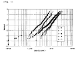
- FIG. 4 shows a measurement result as a Weibull plot.
- FIG. 4 is called the Weibull plot and it is often used when describing a semiconductor device failure distribution such as TDDB.
- Its abscissa represents a charge amount Qbd (C/cm 2 ) applied to the oxide film as an index while its ordinate represents lnln (1/(1-F(t))).
- F(t) represents a cumulative failure rate and, for example, a Weibull value when the cumulative failure rate is 50% is -0.37.
Landscapes
- Formation Of Insulating Films (AREA)
- Testing Or Measuring Of Semiconductors Or The Like (AREA)
Abstract
Description
- The present invention relates to a method for forming, e.g., a thin oxide film on a silicon wafer.
- Semiconductor devices such as an MOS (Metal Oxide Semiconductor) capacitor or a transistor are formed on a main surface of a semiconductor silicon wafer. A thickness of an insulator film such as a gate oxide film formed in such semiconductor devices is reduced with realization of high densities of the semiconductor devices and, on the other hand, decreasing a power supply voltage is difficult, whereby the insulator film is used with a high electric field intensity. Therefore, an insulator film having a higher quality is required.
- As a reduction in film thickness of silicon oxide films involved by miniaturization advances, an unevenness allowable range for an oxide film thickness closes on a value corresponding to several atoms as an absolute value. Further, since insulation properties are degraded due to a direct tunnel current and gate leak increases in time of applying an electric field to an oxide film with a reduction in film thickness, new High-k materials have been studied with respect to a limit as the insulator film. However, in case that such new materials are used, a silicon oxide film is grown thinly and a High-k material is grown thereon. Therefore, accurately forming a thin oxide film is becoming more important.
- An oxidation technique and others have been examined as control over growth of such an oxide film. Although a crystal orientation (B. E. Deal, J. Electrochem. Soc., 125, 576 (1978)., and E. A. Irene et. al., J. Electrochem. Soc., 133, 1253 (1986)., and S. I. Raider et. al., J. Electrochem. Soc., 127, 1783 (1980).) and a dopant (B. E. Deal et. al., J. Electrochem. Soc., 112, 430 (1965)., and C.P. Ho et. al., J. Electrochem. Soc., 125, 665 (1978)., and Seong S. Choi et. al., Appl. Phys. Lett., 51, 1001 (1987)., and C. P. Ho et. al., J. Electrochem. Soc., 126, 1516, 1523 (1979).) and others are well known as influences of a silicon wafer itself, parameters other than those described above have been rarely reported in the era of a so-called ultrathin oxide film having a thickness of nearly 5 nm or below.
- In regard to crystal orientation dependence, an oxidation rate has a relationship of <111> > <100> irrespective of wet oxidation or dry oxidation. This plane orientation dependence of oxidation rate has been explained with a silicon atom density difference between crystal planes of respective plane orientations. A surface density is 7.85×10¹⁴(/cm2) in <111> while a surface density is 6.8×10¹⁴(/cm2) in <100>, and the oxidation rate rises as the surface density increases.
- However, there is complexity between <110> plane and <111> plane. The surface density is 7.85×10¹⁹(/cm2) in <111> while a surface density is 9.6×10¹⁴(/cm2) in <110>, and an oxidation rate relationship can be assumed to be <110> > <111> in terms of the surface density argument. This order is provided when an oxide film is as thin as approximately 15 nm, but the order is reversed and <111> > <110> is achieved when the film thickness increases. Such a complicated behavior has been still argued.
- Further, although a dopant acts in a direction along which the oxidation rate is accelerated, in more detail, if the dopant is phosphorus, a degree of an increase in oxidation rate rises as a temperature is reduced, and a rate increasing effect is decreased as the temperature is increased. Arsenic has the same tendency. On the other hand, in case of boron, the rate increasing effect is maintained even though the temperature is high.
- Furthermore, according to recent studies (e.g, "Growth Kinetics of Very Thin Silicon Oxide Layers Monitored in Real-time by RHEED-AES" by Takakuwa, Surface Science, 23, 536 (2002).), models in which both vacancies that are point defects produced due to an interface damage and emitted Si atoms play the role of promoting an oxidizing reaction have been proposed. These models attempt an explanation of an oxidation mechanism in a thin-film region in particular which cannot be explained with a conventional Deal-Grove model as detailed analysis of the oxidizing reaction advances.
- However, the above-described conventional parameters alone are insufficient to provide a uniform film thickness when forming, e.g., an ultrathin oxide film, and new parameters for accurately adjusting oxidizing conditions are required.
- Therefore, in view of the above-described problems, it is an object of the present invention to provide a method for forming an oxide film by which oxidizing conditions can be adjusted based on a state of a surface and/or a surface layer of a silicon wafer before forming an oxide film and, e.g., an ultrathin oxide film can be thereby accurately formed.
- To achieve this object, according to the present invention, there is provided a method for forming an oxide film on a silicon wafer, comprising: measuring surface roughness of the silicon wafer and/or crystallinity in a surface layer portion of the silicon wafer in advance; adjusting oxidizing conditions for the silicon wafer based on the measurement value; and forming the oxide film on the silicon wafer under the adjusted oxidizing conditions.
- As described above, according to the method for forming an oxide film of the present invention, since the oxidizing conditions can be adjusted based on the surface roughness and/or the crystallinity of the silicon wafer, the measurement can be performed by the simple method and the oxidizing conditions can be accurately adjusted. Furthermore, according to the method of the present invention, since the oxidizing conditions can be adjusted based on the surface roughness or the crystallinity, even if wafers have the same material or the same crystal orientation which has been utilized as a conventional parameter, oxidation rates of the respective wafers can be grasped, each oxide film can be accurately formed, and even a thin oxide film can be formed with a uniform film thickness on each wafer. Moreover, as different from a conventional oxidation rate parameter, the surface roughness or the crystallinity can be adjusted by e.g., repolishing after the measurement and before the formation of the oxide film, whereby the oxidation rate for the wafer can be adjusted and the oxide film having a good quality can be formed.
- Additionally, since the crystallinity and the surface roughness have a close relationship, the oxidizing conditions for the silicon wafer can be accurately adjusted by measuring both of them or checking one of them.
Further, an oxidation rate of a wafer having excellent surface roughness or crystallinity becomes uniform within a wafer plane, and an oxide film having a thickness that is uniform within the wafer plane can be readily formed, whereby a wafer having excellent surface roughness or crystallinity can be sorted to form an oxide film. - At this time, it is preferable that the surface roughness of the silicon wafer is measured by using an AFM to measure an Ra value of the surface roughness of the silicon wafer.
As described above, according to the present invention, to measure the surface roughness, the Ra value of the surface roughness of the silicon wafer can be measured by the generally adopted AFM. - At this time, it is preferable to adjust the oxidizing conditions for the silicon wafer based on whether the measured Ra value of the surface roughness is not more than 0.17 nm.
As described above, when the Ra value of the surface roughness measured by the AFM is not more than 0.17 nm, the oxidation rate is sufficiently small, a film thickness of the oxide film can be readily controlled, the oxide film that is uniform within the wafer plane can be readily formed, and hence the oxidizing conditions can be further easily adjusted by, e.g., sorting each wafer on which the oxide film is to be formed together based on the above-described value. - Furthermore, it is preferable that the crystallinity in the surface layer portion of the silicon wafer is measured by measuring a full width at half maximum of a rocking curve obtained by X-ray diffraction measurement.
When the crystallinity is measured by measuring a full width at half maximum of the rocking curve obtained by the X-ray diffraction measurement as described above, a numerical value accurately indicating the crystallinity can be grasped, thus further readily adjusting the oxidizing conditions. - At this time, it is preferable to adjust the oxidizing conditions for the silicon wafer based on whether the measured full width at half maximum of the rocking curve is not more than 0.00074°.
When the full width at half maximum of the rocking curve obtained by the X-ray diffraction measurement is not more than 0.00074° as described above, a film thickness of the oxide film can be easily controlled since the oxidation rate is sufficiently low, the oxide film that is uniform within the wafer plane can be easily formed, and hence the oxidizing conditions can be further readily adjusted by, e.g., sorting wafers that are put into the same batch based on the above-described value. - At this time, it is preferable to set a thickness of the oxide film to be formed to 5 nm or below.
Even in the case of an ultrathin oxide film of 5 nm or below, according to the method for forming an oxide film of the present invention, the oxidation rate for each silicon wafer can be accurately grasped and thereby the oxide film that has a good film thickness accuracy and is uniform within the wafer plane can be formed. - As described above, according to the method for forming an oxide film on a silicon wafer of the present invention, since the oxidizing conditions can be adjusted based on the surface roughness or the crystallinity before forming the oxide film on the silicon wafer, as different from the conventional oxidation rate parameter using a dope amount or a crystal orientation, oxidation rate of wafers having the same material or the same crystal orientation can be grasped, and the oxide film having a desired thickness can be accurately formed by the simple method. Moreover, since wafers having good surface roughness or crystallinity have oxidation rates, which are substantially the same within the planes thereof, such wafers can be selected to form the excellent oxide film having a thickness that is uniform within the wafer plane. Therefore, in the present invention, if the measurement is performed and a result is poor surface roughness or poor crystallinity, e.g., repolishing is performed and thereby the oxide film having a film thickness that is uniform within the wafer plane can be efficiently formed based on the simple method. In particular, according to the present invention, even an ultrathin oxide film of 5 nm or below can be formed by accurately controlling its thickness.
-
-
FIG. 1 is a graph showing a relationship between surface roughness and an oxide film thickness of a silicon wafer; -
FIG. 2 is a view showing an outline of X-ray diffraction measurement; -
FIG. 3 is a graph showing a relationship between a full width at half maximum of a rocking curve and surface roughness; and -
FIG. 4 is a graph showing Weibull plot of a TDDB evaluation result. - For example, when forming an ultrathin oxide film, there is a problem that unevenness in film thickness is observed in the formed oxide film due to a difference in oxidation rate between respective wafers even though the wafers have the same specifications.
- In regard to this point, to first examine a relationship between surface roughness and an oxidation rate, the present inventors formed an oxide film on each of wafers having different surface roughness values under the same conditions. Consequently, as shown in
FIG. 1 representing a relationship between an oxide film thickness and surface roughness, they discovered that the oxidation rate and the surface roughness have a correlation since a formed oxide film is thin (a lower oxidation rate) in a wafer having a smaller surface roughness value. - Then, surface roughness of a silicon wafer and crystallinity in a surface layer portion of the silicon wafer were examined. The surface roughness was examined by measuring an Ra value by an AFM, and the crystallinity was examined by performing X-ray diffraction measurement with respect to a portion of the wafer near the outermost surface in an In-Plane arrangement to obtain a full width at half maximum of a rocking curve. A Cu ray was used as the X-ray.
Consequently, as shown inFIG. 3 depicting a relationship between the surface roughness and the full width at half maximum, it can be understood that both of them have a good correlation. This result reveals a fact that, as findings of an oxidation mechanism, especially a behavior on an initial stage of oxidation, a wafer having large surface roughness has a high oxidation rate, but this tendency has a close relationship with silicon surface crystallinity. That is, it was considered that, when the crystallinity is disordered (the surface roughness is increased), silicon-silicon bonding is apt to be cleaved and oxygen atoms can readily enter this cleavage whereby the oxidation rate increases. - As a result of the above-described review, the present inventors discovered that, when the surface roughness of a silicon wafer and/or the crystallinity in a surface layer portion of the silicon wafer is measured and oxidizing conditions are adjusted based on a measurement value to form the oxide film, the oxide film having a uniform and accurate thickness can be formed even tough it is an ultrathin oxide film, thereby bringing the present invention to completion.
- Although an embodiment of a method for forming an oxide film on a silicon wafer according to the present invention will now be described in detail hereinafter, the present invention is not restricted thereto.
- In the method for forming an oxide film according to the present invention, surface roughness of a silicon wafer and/or crystallinity in a surface layer portion of the silicon wafer is first measured.
Both or one of the surface roughness and the crystallinity may be measured. Both of them have a close correlation, an oxidation rate can be sufficiently grasped by just measuring one of them, and both of them may be measured for a further accuracy. - At this time, it is preferable to measure the surface roughness of the silicon wafer by measuring an Ra value of the surface roughness by using an AFM (Atomic Force Microscope). As described above, the Ra value that is generally utilized to represent the surface roughness can be readily obtained by using the AFM.
- Further, it is preferable to measure the crystallinity in the surface layer portion of the silicon wafer by measuring a full width at half maximum of a rocking curve obtained by X-ray diffraction measurement.
When a full width at half maximum of a rocking curve obtained by the X-ray diffraction measurement is used as described above, the crystallinity of the wafer surface layer portion can be accurately grasped as a numerical value.
Although a method of this X-ray diffraction measurement is not restricted in particular, for example, a Cu ray may be used as the X-ray, and the measurement can be performed in an In-Plane arrangement.FIG. 2 shows an outline of the X-ray diffraction measurement in this case. An X-ray reflecting position inFIG. 2 changes when an Si crystal lattice expands or contracts due to a damage. - Then, in the present invention, oxidizing conditions for the silicon wafer are adjusted based on a measurement value obtained from the measurement as described above.
Since an oxidation rate of the silicon wafer is low when the surface roughness is small (the crystallinity is good), the oxidizing conditions can be readily adjusted based on the measurement value obtained from the measurement as described above. At this time, the oxidizing conditions to be adjusted are not restricted in particular, and an oxidation time, an oxidation temperature and others can be adjusted. Additionally, the oxidizing conditions can be adjusted by e.g., oxidizing wafers having substantially the same surface roughness (the crystallinity) in the same batch to form an oxide film having a uniform thickness on each of wafers in the batch.
Further, for example, when wafers having the same surface roughness/crystallinity are utilized as film thickness monitors, dissociation of film thicknesses from actual wafers can be dissipated, thereby suppressing unevenness in oxide film between batches. - At this time, when the Ra value of the surface roughness is measured by using the AFM, it is preferable to adjust the oxidizing conditions for the silicon wafer based on whether the Ra value is not more than 0.17 nm.
When the Ra value is not more than 0.17 nm as described above, since the oxidation rate is sufficiently small as shown inFIG. 1 , a film thickness of the oxide film can be readily controlled, and the oxide film that is uniform within a wafer plane can be easily formed, whereby the oxidizing conditions can be further readily adjusted by, e.g., sorting wafers that are put into the same batch based on the above-described value. - Furthermore, when a full width at half maximum of the rocking curve is measured based on the X-ray diffraction measurement, it is preferable to adjust the oxidizing conditions for the silicon wafer based on whether this full width at half maximum is not more than 0.00074°.
When the full width at half maximum of the silicon wafer surface layer portion is not more than 0.00074° as described above, the Ra value of the surface roughness of this surface is approximately 0.17 nm or below as shown inFIG. 3 , the oxidation rate is thus sufficiently low, a film thickness of the oxide film can be easily controlled, and the oxide film that is uniform within the wafer plane can be readily formed, whereby the oxidizing conditions can be further easily adjusted by, e.g., sorting wafers that are put into the same batch based on the above-described value. - Additionally, for example, an ultrathin oxide film may be formed on each wafer having the measurement value or a lower value alone, each wafer having the measurement value or a larger value may be subjected to, e.g., repolishing so that each wafer has the measurement value or a smaller value, and the oxide film can be formed thereon.
- Then, in the present invention, the oxide film is formed on each silicon wafer under the thus adjusted oxidizing conditions.
At this time, a method for forming the oxide film is not restricted in particular, and a wafer can be subjected to, e.g., dry oxidation in a vertical heat treating furnace, thereby forming the oxide film under the adjusted oxidizing conditions. - At this time, it is preferable to form the oxide film having a thickness of 5 nm or below.
As described above, since the oxidation rate can be accurately grasped by using the method for forming an oxide film according to the present invention, an oxide film having an accurate thickness can be formed with high precision when forming an ultrathin oxide film of 5 nm or below, and an oxide film thickness within a wafer plane can have excellent uniformity. Therefore, it is possible to sufficiently cope with a recent cutting-edge device using an ultrathin oxide film. - As described above, according to the present invention, since the oxidizing conditions can be adjusted by measuring the surface roughness and/or the crystallinity, the oxidizing conditions can be accurately adjusted by the simple method, thereby accurately controlling a thickness of the oxide film.
- The present invention will now be more specifically explained hereinafter based on an example, but the present invention is not restricted thereto.
- Samples are first fabricated. P-type boron-doped semiconductor silicon wafers each having a diameter of 200 mm were prepared as samples.
The thus prepared semiconductor silicon wafers were subjected to polishing and others to provide wafers on 5 standards (A, B, C, D and E) having different surface roughness values obtained by measurement using an AFM. These semiconductor silicon wafers were placed on a boat to be put into a vertical heat treating furnace, a film thickness of 3 nm was determined as a target, and a heat treatment was performed at 800 °C in a dry oxygen atmosphere (an oxygen partial pressure of 0.1 atom: diluted oxidation) to form an oxide film on each wafer main surface. Then, an ellipsometer (λ=633 nm) was utilized to measure an oxide film thickness on each wafer (A, B, C, D or E).FIG. 1 shows a relationship between this oxide film thickness and the surface roughness. - As apparent from
FIG. 1 , it can be understood that a thickness of the oxide film is small (an oxidation rate is low) as the surface roughness is small (as the surface is flat). Therefore, it can be also understood that using such a measurement result enables adjusting oxidizing conditions. - A surface layer portion of each of these semiconductor silicon wafers (A, B, C, D and E) before a heat treatment was subjected to In-plane diffraction (see
FIG. 2 ) as X-ray diffraction measurement to obtain a rocking curve, and its full width at half maximum was measured.FIG. 3 shows a relationship between the full width at half maximum and the surface roughness at this time.
As apparent fromFIG. 3 , it can be understood that the surface roughness and crystallinity have a close correlation, and both of them can be measured to be used as oxidation rate parameters. - Then, these semiconductor wafers (A, B, C, D and E) were placed on the boat and put into the vertical heat treating furnace, each oxide film was further formed by dry oxidation at 800°C until reaching a thickness of 5 nm, thereby forming each gate oxide film.
Subsequently, these semiconductor wafers (A, B, C, D and E) were put into a CVD furnace, and a polysilicon layer was grown on each gate oxide film while doping phosphorus. A thickness of the grown polysilicon layer was approximately 300 nm, and a resistance value was approximately 25 Q/sq in terms of sheet resistance. - Then, these semiconductor silicon wafers (A, B, C, D and E) were subjected to patterning using a photolithography technology and polysilicon layer removal based on etching, and 100 MOS capacitors using the polysilicon layer as an electrode were fabricated within each semiconductor silicon wafer plane. It is to be noted that, as polysilicon etching after photolithography, wet etching using a hydrofluoricnitric acid was performed. At last, to remove the silicon oxide film formed on each semiconductor silicon wafer back surface, a resist was applied to each semiconductor silicon wafer main surface, and wet etching using a diluted hydrofluoric acid was carried out to remove the silicon oxide film on the wafer back surface.
- An electric field stress was applied to the gate oxide film by using a constant-current TDDB method for applying a constant current to each processed semiconductor wafer (A, B, C, D or E) until the gate oxide film is destroyed. The applied current stress was 0.001 A/cm2, and a measurement temperature was set to 100°C while considering a reduction in measurement time. A tester connected to a fully-automatic prober was used for the measurement. An electrode area in this example was 4 mm2.
FIG. 4 shows a measurement result as a Weibull plot. -
FIG. 4 is called the Weibull plot and it is often used when describing a semiconductor device failure distribution such as TDDB. Its abscissa represents a charge amount Qbd (C/cm2) applied to the oxide film as an index while its ordinate represents lnln (1/(1-F(t))). Here, F(t) represents a cumulative failure rate and, for example, a Weibull value when the cumulative failure rate is 50% is -0.37. - As can be seen from
FIG. 4 , degradation in TDDB characteristics (a reduction in reliability) was observed in the wafers A and B each having Ra equal to or above 0.18 nm and a full width at half maximum higher than 0.00074°. As a result, it can be understood that a degree of degradation in TDDB characteristics is small in a silicon wafer having Ra of 0.17 nm or below and a full width at half maximum of 0.00074° or below. That is considered to be because an oxidation rate is sufficiently low and control over an oxide film thickness is easy in such a silicon wafer, an accurate film thickness can be thus obtained, and the oxidation rate is relatively uniform within a wafer plane, whereby film thickness uniformity of the oxide film is high. - It is to be noted that the present invention is not restricted to the foregoing embodiment. The embodiment is just an exemplification, and any examples that have substantially the same configuration and demonstrate the same functions and effects as the technical concept described in claims of the present invention are included in the technical scope of the present invention.
Claims (6)
- A method for forming an oxide film on a silicon wafer, comprising: measuring surface roughness of the silicon wafer and/or crystallinity in a surface layer portion of the silicon wafer in advance; adjusting oxidizing conditions for the silicon wafer based on the measurement value; and forming the oxide film on the silicon wafer under the adjusted oxidizing conditions.
- The method for forming an oxide film on a silicon wafer according to claim 1, wherein the surface roughness of the silicon wafer is measured by using an AFM to measure an Ra value of the surface roughness of the silicon wafer.
- The method for forming an oxide film on a silicon wafer according to claim 2, wherein the oxidizing conditions for the silicon wafer are adjusted based on whether the measured Ra value of the surface roughness is not more than 0.17 nm.
- The method for forming an oxide film on a silicon wafer according to any one of claims 1 to 3, wherein the crystallinity in the surface layer portion of the silicon wafer is measured by measuring a full width at half maximum of a rocking curve obtained by X-ray diffraction measurement.
- The method for forming an oxide film on a silicon wafer according to claim 4, wherein the oxidizing conditions for the silicon wafer are adjusted based on whether the measured full width at half maximum of the rocking curve is not more than 0.00074°.
- The method for forming an oxide film on a silicon wafer according to any one of claims 1 to 5, wherein a thickness of the oxide film to be formed is set to 5 nm or below.
Applications Claiming Priority (2)
| Application Number | Priority Date | Filing Date | Title |
|---|---|---|---|
| JP2008115672A JP5272496B2 (en) | 2008-04-25 | 2008-04-25 | Method for forming oxide film on silicon wafer |
| PCT/JP2009/001281 WO2009130847A1 (en) | 2008-04-25 | 2009-03-24 | Method for formation of oxide film for silicon wafer |
Publications (3)
| Publication Number | Publication Date |
|---|---|
| EP2273539A1 true EP2273539A1 (en) | 2011-01-12 |
| EP2273539A4 EP2273539A4 (en) | 2013-03-27 |
| EP2273539B1 EP2273539B1 (en) | 2017-06-28 |
Family
ID=41216590
Family Applications (1)
| Application Number | Title | Priority Date | Filing Date |
|---|---|---|---|
| EP09735085.4A Active EP2273539B1 (en) | 2008-04-25 | 2009-03-24 | Method for formation of oxide film for silicon wafer |
Country Status (6)
| Country | Link |
|---|---|
| US (1) | US8043871B2 (en) |
| EP (1) | EP2273539B1 (en) |
| JP (1) | JP5272496B2 (en) |
| KR (1) | KR101559985B1 (en) |
| CN (1) | CN102017098B (en) |
| WO (1) | WO2009130847A1 (en) |
Families Citing this family (9)
| Publication number | Priority date | Publication date | Assignee | Title |
|---|---|---|---|---|
| US8921992B2 (en) | 2013-03-14 | 2014-12-30 | Raytheon Company | Stacked wafer with coolant channels |
| US9842762B1 (en) * | 2016-11-11 | 2017-12-12 | Globalfoundries Inc. | Method of manufacturing a semiconductor wafer having an SOI configuration |
| JP6692306B2 (en) * | 2017-02-09 | 2020-05-13 | 株式会社東芝 | Semiconductor device, manufacturing method of semiconductor device, inverter circuit, drive device, vehicle, and elevator |
| KR102014926B1 (en) | 2017-10-31 | 2019-08-27 | 에스케이실트론 주식회사 | Method for predicting thickness of oxide layer of silicon wafer |
| CN108054112B (en) * | 2017-12-21 | 2021-11-30 | 重庆超硅半导体有限公司 | Method for testing minority carrier lifetime of IC-level silicon wafer |
| KR102094153B1 (en) * | 2018-10-16 | 2020-03-27 | 한국표준과학연구원 | Method for Forming High-k Insulating Film of MOS Transistor |
| CN111106027A (en) * | 2019-12-23 | 2020-05-05 | 武汉大学 | A measurement and modification system for SOI top silicon wafer |
| CN112857270B (en) * | 2021-01-08 | 2022-12-09 | 上海科技大学 | Method for in-situ real-time quantitative detection of film roughness by using RHEED |
| JP7616022B2 (en) * | 2021-11-08 | 2025-01-17 | 信越半導体株式会社 | Method for evaluating oxide film thickness and method for manufacturing silicon substrate with oxide film |
Family Cites Families (6)
| Publication number | Priority date | Publication date | Assignee | Title |
|---|---|---|---|---|
| JPH0513395A (en) * | 1991-07-02 | 1993-01-22 | Tadahiro Omi | Silicon wafer and cleaning method |
| JP3417665B2 (en) * | 1994-07-07 | 2003-06-16 | 株式会社東芝 | Method for manufacturing semiconductor device |
| US6020247A (en) * | 1996-08-05 | 2000-02-01 | Texas Instruments Incorporated | Method for thin film deposition on single-crystal semiconductor substrates |
| AU2003264642B2 (en) * | 2002-12-02 | 2009-08-06 | Tadahiro Ohmi | Semiconductor Device and Method of Manufacturing the Same |
| US6723666B1 (en) * | 2003-03-06 | 2004-04-20 | Advanced Micro Devices, Inc. | Method for reducing gate oxide surface irregularities |
| WO2006099171A2 (en) * | 2005-03-11 | 2006-09-21 | The Arizona Boar Of Regents, A Body Corporate Acting On Behalf Of Arizona State University | NOVEL GeSiSn-BASED COMPOUNDS, TEMPLATES, AND SEMICONDUCTOR STRUCTURES |
-
2008
- 2008-04-25 JP JP2008115672A patent/JP5272496B2/en active Active
-
2009
- 2009-03-24 WO PCT/JP2009/001281 patent/WO2009130847A1/en not_active Ceased
- 2009-03-24 KR KR1020107023274A patent/KR101559985B1/en active Active
- 2009-03-24 US US12/921,492 patent/US8043871B2/en active Active
- 2009-03-24 EP EP09735085.4A patent/EP2273539B1/en active Active
- 2009-03-24 CN CN2009801141292A patent/CN102017098B/en active Active
Also Published As
| Publication number | Publication date |
|---|---|
| EP2273539B1 (en) | 2017-06-28 |
| WO2009130847A1 (en) | 2009-10-29 |
| KR20110014978A (en) | 2011-02-14 |
| US8043871B2 (en) | 2011-10-25 |
| CN102017098B (en) | 2013-01-30 |
| EP2273539A4 (en) | 2013-03-27 |
| JP5272496B2 (en) | 2013-08-28 |
| JP2009267125A (en) | 2009-11-12 |
| US20110033958A1 (en) | 2011-02-10 |
| CN102017098A (en) | 2011-04-13 |
| KR101559985B1 (en) | 2015-10-13 |
Similar Documents
| Publication | Publication Date | Title |
|---|---|---|
| US8043871B2 (en) | Method for forming oxide film on silicon wafer | |
| US7103484B1 (en) | Non-contact methods for measuring electrical thickness and determining nitrogen content of insulating films | |
| Nieh et al. | Electrical characterization and material evaluation of zirconium oxynitride gate dielectric in TaN-gated NMOSFETs with high-temperature forming gas annealing | |
| Osada et al. | Effect of stress in the deposited silicon nitride films on boron diffusion of silicon | |
| Wilk et al. | Electrical characteristics of high-quality sub-25-/spl Aring/oxides grown by ultraviolet ozone exposure at low temperature | |
| Miura et al. | Effect of mechanical stress on reliability of gate-oxide film in MOS transistors | |
| Van Elshocht et al. | Metallorganic chemical vapor deposition of dysprosium scandate high-k layers using mmp-type precursors | |
| Clark et al. | Physical and electrical effects of the Dep-Anneal-Dep-Anneal (DADA) process for HfO2 in high K/metal gate stacks | |
| Cherif et al. | Investigation of structural properties, electrical and dielectrical characteristics of Al/Dy2O3/porous Si heterostructure | |
| Tarek et al. | Bilayer gate dielectric of ZrO2 and Ho2O3 on 4H–SiC substrate: structural and electrical characterization | |
| Cresswell et al. | CD reference materials for sub-10th um applications | |
| CN114068343B (en) | Monitoring method of thickness of gate dielectric layer | |
| US6821892B1 (en) | Intelligent wet etching tool as a function of chemical concentration, temperature and film loss | |
| CN107492492A (en) | The monitoring method of annealing device technological ability | |
| US7745236B2 (en) | Floating gate process methodology | |
| CN119534398B (en) | A method for measuring the size of oxygen precipitation in silicon wafers | |
| JPH08321443A (en) | Method for manufacturing semiconductor device | |
| JP5217353B2 (en) | Insulating film formation method | |
| De Witte et al. | In-line electrical metrology for high-K gate dielectrics deposited by atomic layer CVD | |
| Hoff | Growth and metrology of silicon oxides on silicon carbide | |
| JP5729098B2 (en) | Evaluation method of silicon single crystal wafer | |
| Wu et al. | Characterization of ultrathin oxide prepared by low‐temperature wafer loading and nitrogen preannealing before oxidation | |
| Mairhofer | Electronic transport phenomena in ultrascaled aluminum layers | |
| Tallarida et al. | Surface morphology of nitrided thin thermal SiO2 studied by atomic force microscopy | |
| Trabzon et al. | The degradation of MOSFETs induced by the via etching of interlayer low-k polymers |
Legal Events
| Date | Code | Title | Description |
|---|---|---|---|
| PUAI | Public reference made under article 153(3) epc to a published international application that has entered the european phase |
Free format text: ORIGINAL CODE: 0009012 |
|
| 17P | Request for examination filed |
Effective date: 20101021 |
|
| AK | Designated contracting states |
Kind code of ref document: A1 Designated state(s): AT BE BG CH CY CZ DE DK EE ES FI FR GB GR HR HU IE IS IT LI LT LU LV MC MK MT NL NO PL PT RO SE SI SK TR |
|
| AX | Request for extension of the european patent |
Extension state: AL BA RS |
|
| DAX | Request for extension of the european patent (deleted) | ||
| A4 | Supplementary search report drawn up and despatched |
Effective date: 20130225 |
|
| RIC1 | Information provided on ipc code assigned before grant |
Ipc: H01L 21/66 20060101ALI20130219BHEP Ipc: H01L 21/316 20060101AFI20130219BHEP |
|
| 17Q | First examination report despatched |
Effective date: 20131114 |
|
| RAP1 | Party data changed (applicant data changed or rights of an application transferred) |
Owner name: SHIN-ETSU HANDOTAI CO., LTD. |
|
| GRAP | Despatch of communication of intention to grant a patent |
Free format text: ORIGINAL CODE: EPIDOSNIGR1 |
|
| STAA | Information on the status of an ep patent application or granted ep patent |
Free format text: STATUS: GRANT OF PATENT IS INTENDED |
|
| INTG | Intention to grant announced |
Effective date: 20170125 |
|
| GRAS | Grant fee paid |
Free format text: ORIGINAL CODE: EPIDOSNIGR3 |
|
| GRAA | (expected) grant |
Free format text: ORIGINAL CODE: 0009210 |
|
| STAA | Information on the status of an ep patent application or granted ep patent |
Free format text: STATUS: THE PATENT HAS BEEN GRANTED |
|
| AK | Designated contracting states |
Kind code of ref document: B1 Designated state(s): AT BE BG CH CY CZ DE DK EE ES FI FR GB GR HR HU IE IS IT LI LT LU LV MC MK MT NL NO PL PT RO SE SI SK TR |
|
| REG | Reference to a national code |
Ref country code: GB Ref legal event code: FG4D |
|
| REG | Reference to a national code |
Ref country code: CH Ref legal event code: EP |
|
| REG | Reference to a national code |
Ref country code: AT Ref legal event code: REF Ref document number: 905541 Country of ref document: AT Kind code of ref document: T Effective date: 20170715 |
|
| REG | Reference to a national code |
Ref country code: IE Ref legal event code: FG4D |
|
| REG | Reference to a national code |
Ref country code: DE Ref legal event code: R096 Ref document number: 602009046852 Country of ref document: DE |
|
| PG25 | Lapsed in a contracting state [announced via postgrant information from national office to epo] |
Ref country code: GR Free format text: LAPSE BECAUSE OF FAILURE TO SUBMIT A TRANSLATION OF THE DESCRIPTION OR TO PAY THE FEE WITHIN THE PRESCRIBED TIME-LIMIT Effective date: 20170929 Ref country code: FI Free format text: LAPSE BECAUSE OF FAILURE TO SUBMIT A TRANSLATION OF THE DESCRIPTION OR TO PAY THE FEE WITHIN THE PRESCRIBED TIME-LIMIT Effective date: 20170628 Ref country code: LT Free format text: LAPSE BECAUSE OF FAILURE TO SUBMIT A TRANSLATION OF THE DESCRIPTION OR TO PAY THE FEE WITHIN THE PRESCRIBED TIME-LIMIT Effective date: 20170628 Ref country code: HR Free format text: LAPSE BECAUSE OF FAILURE TO SUBMIT A TRANSLATION OF THE DESCRIPTION OR TO PAY THE FEE WITHIN THE PRESCRIBED TIME-LIMIT Effective date: 20170628 Ref country code: NO Free format text: LAPSE BECAUSE OF FAILURE TO SUBMIT A TRANSLATION OF THE DESCRIPTION OR TO PAY THE FEE WITHIN THE PRESCRIBED TIME-LIMIT Effective date: 20170928 |
|
| REG | Reference to a national code |
Ref country code: NL Ref legal event code: MP Effective date: 20170628 |
|
| REG | Reference to a national code |
Ref country code: LT Ref legal event code: MG4D |
|
| REG | Reference to a national code |
Ref country code: AT Ref legal event code: MK05 Ref document number: 905541 Country of ref document: AT Kind code of ref document: T Effective date: 20170628 |
|
| PG25 | Lapsed in a contracting state [announced via postgrant information from national office to epo] |
Ref country code: NL Free format text: LAPSE BECAUSE OF FAILURE TO SUBMIT A TRANSLATION OF THE DESCRIPTION OR TO PAY THE FEE WITHIN THE PRESCRIBED TIME-LIMIT Effective date: 20170628 Ref country code: SE Free format text: LAPSE BECAUSE OF FAILURE TO SUBMIT A TRANSLATION OF THE DESCRIPTION OR TO PAY THE FEE WITHIN THE PRESCRIBED TIME-LIMIT Effective date: 20170628 Ref country code: BG Free format text: LAPSE BECAUSE OF FAILURE TO SUBMIT A TRANSLATION OF THE DESCRIPTION OR TO PAY THE FEE WITHIN THE PRESCRIBED TIME-LIMIT Effective date: 20170928 Ref country code: LV Free format text: LAPSE BECAUSE OF FAILURE TO SUBMIT A TRANSLATION OF THE DESCRIPTION OR TO PAY THE FEE WITHIN THE PRESCRIBED TIME-LIMIT Effective date: 20170628 |
|
| PG25 | Lapsed in a contracting state [announced via postgrant information from national office to epo] |
Ref country code: RO Free format text: LAPSE BECAUSE OF FAILURE TO SUBMIT A TRANSLATION OF THE DESCRIPTION OR TO PAY THE FEE WITHIN THE PRESCRIBED TIME-LIMIT Effective date: 20170628 Ref country code: CZ Free format text: LAPSE BECAUSE OF FAILURE TO SUBMIT A TRANSLATION OF THE DESCRIPTION OR TO PAY THE FEE WITHIN THE PRESCRIBED TIME-LIMIT Effective date: 20170628 Ref country code: EE Free format text: LAPSE BECAUSE OF FAILURE TO SUBMIT A TRANSLATION OF THE DESCRIPTION OR TO PAY THE FEE WITHIN THE PRESCRIBED TIME-LIMIT Effective date: 20170628 Ref country code: SK Free format text: LAPSE BECAUSE OF FAILURE TO SUBMIT A TRANSLATION OF THE DESCRIPTION OR TO PAY THE FEE WITHIN THE PRESCRIBED TIME-LIMIT Effective date: 20170628 Ref country code: AT Free format text: LAPSE BECAUSE OF FAILURE TO SUBMIT A TRANSLATION OF THE DESCRIPTION OR TO PAY THE FEE WITHIN THE PRESCRIBED TIME-LIMIT Effective date: 20170628 |
|
| REG | Reference to a national code |
Ref country code: FR Ref legal event code: PLFP Year of fee payment: 10 |
|
| PG25 | Lapsed in a contracting state [announced via postgrant information from national office to epo] |
Ref country code: PL Free format text: LAPSE BECAUSE OF FAILURE TO SUBMIT A TRANSLATION OF THE DESCRIPTION OR TO PAY THE FEE WITHIN THE PRESCRIBED TIME-LIMIT Effective date: 20170628 Ref country code: IS Free format text: LAPSE BECAUSE OF FAILURE TO SUBMIT A TRANSLATION OF THE DESCRIPTION OR TO PAY THE FEE WITHIN THE PRESCRIBED TIME-LIMIT Effective date: 20171028 Ref country code: IT Free format text: LAPSE BECAUSE OF FAILURE TO SUBMIT A TRANSLATION OF THE DESCRIPTION OR TO PAY THE FEE WITHIN THE PRESCRIBED TIME-LIMIT Effective date: 20170628 Ref country code: ES Free format text: LAPSE BECAUSE OF FAILURE TO SUBMIT A TRANSLATION OF THE DESCRIPTION OR TO PAY THE FEE WITHIN THE PRESCRIBED TIME-LIMIT Effective date: 20170628 |
|
| REG | Reference to a national code |
Ref country code: DE Ref legal event code: R097 Ref document number: 602009046852 Country of ref document: DE |
|
| PG25 | Lapsed in a contracting state [announced via postgrant information from national office to epo] |
Ref country code: DK Free format text: LAPSE BECAUSE OF FAILURE TO SUBMIT A TRANSLATION OF THE DESCRIPTION OR TO PAY THE FEE WITHIN THE PRESCRIBED TIME-LIMIT Effective date: 20170628 |
|
| PLBE | No opposition filed within time limit |
Free format text: ORIGINAL CODE: 0009261 |
|
| STAA | Information on the status of an ep patent application or granted ep patent |
Free format text: STATUS: NO OPPOSITION FILED WITHIN TIME LIMIT |
|
| 26N | No opposition filed |
Effective date: 20180329 |
|
| PG25 | Lapsed in a contracting state [announced via postgrant information from national office to epo] |
Ref country code: SI Free format text: LAPSE BECAUSE OF FAILURE TO SUBMIT A TRANSLATION OF THE DESCRIPTION OR TO PAY THE FEE WITHIN THE PRESCRIBED TIME-LIMIT Effective date: 20170628 |
|
| REG | Reference to a national code |
Ref country code: CH Ref legal event code: PL |
|
| GBPC | Gb: european patent ceased through non-payment of renewal fee |
Effective date: 20180324 |
|
| PG25 | Lapsed in a contracting state [announced via postgrant information from national office to epo] |
Ref country code: MC Free format text: LAPSE BECAUSE OF FAILURE TO SUBMIT A TRANSLATION OF THE DESCRIPTION OR TO PAY THE FEE WITHIN THE PRESCRIBED TIME-LIMIT Effective date: 20170628 |
|
| REG | Reference to a national code |
Ref country code: BE Ref legal event code: MM Effective date: 20180331 |
|
| REG | Reference to a national code |
Ref country code: IE Ref legal event code: MM4A |
|
| PG25 | Lapsed in a contracting state [announced via postgrant information from national office to epo] |
Ref country code: LU Free format text: LAPSE BECAUSE OF NON-PAYMENT OF DUE FEES Effective date: 20180324 |
|
| PG25 | Lapsed in a contracting state [announced via postgrant information from national office to epo] |
Ref country code: IE Free format text: LAPSE BECAUSE OF NON-PAYMENT OF DUE FEES Effective date: 20180324 |
|
| PG25 | Lapsed in a contracting state [announced via postgrant information from national office to epo] |
Ref country code: BE Free format text: LAPSE BECAUSE OF NON-PAYMENT OF DUE FEES Effective date: 20180331 Ref country code: CH Free format text: LAPSE BECAUSE OF NON-PAYMENT OF DUE FEES Effective date: 20180331 Ref country code: LI Free format text: LAPSE BECAUSE OF NON-PAYMENT OF DUE FEES Effective date: 20180331 Ref country code: GB Free format text: LAPSE BECAUSE OF NON-PAYMENT OF DUE FEES Effective date: 20180324 |
|
| PG25 | Lapsed in a contracting state [announced via postgrant information from national office to epo] |
Ref country code: MT Free format text: LAPSE BECAUSE OF NON-PAYMENT OF DUE FEES Effective date: 20180324 |
|
| PG25 | Lapsed in a contracting state [announced via postgrant information from national office to epo] |
Ref country code: TR Free format text: LAPSE BECAUSE OF FAILURE TO SUBMIT A TRANSLATION OF THE DESCRIPTION OR TO PAY THE FEE WITHIN THE PRESCRIBED TIME-LIMIT Effective date: 20170628 |
|
| PG25 | Lapsed in a contracting state [announced via postgrant information from national office to epo] |
Ref country code: HU Free format text: LAPSE BECAUSE OF FAILURE TO SUBMIT A TRANSLATION OF THE DESCRIPTION OR TO PAY THE FEE WITHIN THE PRESCRIBED TIME-LIMIT; INVALID AB INITIO Effective date: 20090324 Ref country code: PT Free format text: LAPSE BECAUSE OF FAILURE TO SUBMIT A TRANSLATION OF THE DESCRIPTION OR TO PAY THE FEE WITHIN THE PRESCRIBED TIME-LIMIT Effective date: 20170628 |
|
| PG25 | Lapsed in a contracting state [announced via postgrant information from national office to epo] |
Ref country code: CY Free format text: LAPSE BECAUSE OF FAILURE TO SUBMIT A TRANSLATION OF THE DESCRIPTION OR TO PAY THE FEE WITHIN THE PRESCRIBED TIME-LIMIT Effective date: 20170628 Ref country code: MK Free format text: LAPSE BECAUSE OF NON-PAYMENT OF DUE FEES Effective date: 20170628 |
|
| REG | Reference to a national code |
Ref country code: DE Ref legal event code: R079 Ref document number: 602009046852 Country of ref document: DE Free format text: PREVIOUS MAIN CLASS: H01L0021316000 Ipc: H10P0014692000 |
|
| PGFP | Annual fee paid to national office [announced via postgrant information from national office to epo] |
Ref country code: DE Payment date: 20260128 Year of fee payment: 18 |
|
| PGFP | Annual fee paid to national office [announced via postgrant information from national office to epo] |
Ref country code: FR Payment date: 20260209 Year of fee payment: 18 |