EP2269755A2 - Wire cut electric discharge machine with machining state discrimination function - Google Patents
Wire cut electric discharge machine with machining state discrimination function Download PDFInfo
- Publication number
- EP2269755A2 EP2269755A2 EP10164081A EP10164081A EP2269755A2 EP 2269755 A2 EP2269755 A2 EP 2269755A2 EP 10164081 A EP10164081 A EP 10164081A EP 10164081 A EP10164081 A EP 10164081A EP 2269755 A2 EP2269755 A2 EP 2269755A2
- Authority
- EP
- European Patent Office
- Prior art keywords
- voltage
- machining
- output means
- voltage application
- machining gap
- Prior art date
- Legal status (The legal status is an assumption and is not a legal conclusion. Google has not performed a legal analysis and makes no representation as to the accuracy of the status listed.)
- Granted
Links
Images







Classifications
-
- B—PERFORMING OPERATIONS; TRANSPORTING
- B23—MACHINE TOOLS; METAL-WORKING NOT OTHERWISE PROVIDED FOR
- B23H—WORKING OF METAL BY THE ACTION OF A HIGH CONCENTRATION OF ELECTRIC CURRENT ON A WORKPIECE USING AN ELECTRODE WHICH TAKES THE PLACE OF A TOOL; SUCH WORKING COMBINED WITH OTHER FORMS OF WORKING OF METAL
- B23H1/00—Electrical discharge machining, i.e. removing metal with a series of rapidly recurring electrical discharges between an electrode and a workpiece in the presence of a fluid dielectric
- B23H1/02—Electric circuits specially adapted therefor, e.g. power supply, control, preventing short circuits or other abnormal discharges
- B23H1/022—Electric circuits specially adapted therefor, e.g. power supply, control, preventing short circuits or other abnormal discharges for shaping the discharge pulse train
-
- B—PERFORMING OPERATIONS; TRANSPORTING
- B23—MACHINE TOOLS; METAL-WORKING NOT OTHERWISE PROVIDED FOR
- B23H—WORKING OF METAL BY THE ACTION OF A HIGH CONCENTRATION OF ELECTRIC CURRENT ON A WORKPIECE USING AN ELECTRODE WHICH TAKES THE PLACE OF A TOOL; SUCH WORKING COMBINED WITH OTHER FORMS OF WORKING OF METAL
- B23H1/00—Electrical discharge machining, i.e. removing metal with a series of rapidly recurring electrical discharges between an electrode and a workpiece in the presence of a fluid dielectric
- B23H1/02—Electric circuits specially adapted therefor, e.g. power supply, control, preventing short circuits or other abnormal discharges
- B23H1/024—Detection of, and response to, abnormal gap conditions, e.g. short circuits
Definitions
- a so-called "resonance phenomenon” often occurs between a machining power supply and the machining gap.
- a discharge gap length, a workpiece thickness, the state of the flow of the machining fluid, and so on are changed, an electric constant of the machining gap is changed, and a variation of the machining voltage is unavoidable.
- a positive voltage 134 and a negative voltage 136 are alternately output, and an off time 132 is provided after each output of the positive voltage 134 and the negative voltage 136.
- the length of time to apply the positive voltage 134 and the negative voltage 136 is represented by ta, and the length of the off time is represented by tb.
- the machining gap voltage between the wire electrode and the workpiece becomes a trapezoidal wave shaped voltage 138 shown in FIG. 2B .
- FIG. 3B shows the machining gap voltage Vbb of an AC high-frequency voltage 150 (used conventionally) shown in FIG. 11B .
- the machining gap voltages 152, 154, and 156 upon the occurrence of discharge are shown in FIG. 3B .
- the electrostatic attraction force acts between the wire electrode and the workpiece. And so, the wire electrode is bend toward the workpiece by the force, which degrades straightness accuracy.
- the electrostatic attraction force is proportional to the square of the average gap voltage.
- the first D latch 22 receives an output signal 'i' from a Q terminal ofthefirstSRlatch20, the latch instruction 'b' and the reset instruction 'c' from the voltage application timing generator 1.
- the second D latch 23 receives an output signal 'e' from the first comparator 10, the latch instruction 'b', and the reset instruction ⁇ c'.
- the output signals 'h' and 'l' are inverted respectively by the first and second inverters 40 and 41, and then output signals 'm' and 'n' as inversion signals are output from the first and second inverters 40 and 41.
- the output signals 'm' and 'n' and the voltage application instruction 'a' are input to a three-input AND gate 36, and an output signal 'o' from the three-input AND gate 36 is input to the second monostable multi-vibrator 51.
- the second monostable multi-vibrator 51 outputs an output signal 'p'.
- the output signal 'h' is used as a signal (that is, an open signal 'h') for use in the determination of whether or not the machining gap 7 is in an open state.
- the output signal 'p' is used as a signal (that is, a discharge signal 'p') for use in the determination of whether or not the machining gap 7 is in a discharge state.
- the output signal 'l' isusedasasignal (that is, a short signal 'l') for use in the determination of whether or not the machining gap 7 is in a short state.
- the open signal 'h', the discharge signal 'p', and the short signal 'l' are counted by a counting circuit (not shown).
- the machining gap 7 is in a short state, and when the output 'd' of the voltage divider 8 is less than the reference voltage V1 of the first comparator 10, the first SR latch 20 is not set, and the output signal 'i' is held at a low level. In that case, the output 'j' of the *Q terminal of the first D latch 22 is held at a high level and is not changed. Moreover, since the output signal ⁇ f' of the Q terminal of the second D latch 23 is low level, only the output 'k' of the second AND gate 31 is high level (see, 'k1'), and the short signal 'l' is output from the third monostable multi-vibrator 52 (see, ⁇ 11').
- the switching element 4 is turned on based on the voltage application instruction 'a' from the voltage application timing generator 1, the machining gap voltage Vbb is increased, and the output signal 'd' of the voltage divider 8 is more than the respective levels of the reference voltages V1 and V2 of the first and second comparators 10 and 12.
- the first and second SR latches 20 and 21 are set, and the output signal 'i' from the first SR latch 20 and the output signal 'r' from the second SR latch 21 are high level.
- such a case is considered that although the output signal 'd' of the voltage divider 8 is more than the reference voltage V1 of the first comparator 10 by virtue of the application of voltage to the machining gap 7, it does not reaches the reference voltage V2 of the second comparator 12, and the next latch instruction 'b' is output while this state is maintained (in other words, a case in which the output signal 'd' is maintained between the reference values V1 and V2).
- the first SR latch 20 is set, and since the output signal 'e' of the first comparator 10 is high level, the first and second D latches 22 and 23 set a high level signal.
- the second SR latch 21 is not set, and since the output signal 'q' of the second comparator 12 is low level, the third and fourth D latches 24 and 25 set a low level signal.
Landscapes
- Engineering & Computer Science (AREA)
- Mechanical Engineering (AREA)
- Electrical Discharge Machining, Electrochemical Machining, And Combined Machining (AREA)
Abstract
Description
- The present invention relates to a wire cut electric discharge machine. More particularly, the invention relates to a wire cut electric discharge machine with a machining state discrimination function.
- In electric discharge machining, a voltage is applied to an electrode and a workpiece in a machining fluid to generate an arc discharge. The workpiece is melted by heat of the electric discharge, and, at the same time, the machining fluid is rapidly heated to cause vaporizing explosion, and to blow the melted workpiece. This operation is frequently repeated, whereby the machining of the workpiece is progressed. Since small discharge craters generated by electric discharge gather to form a machined surface, the sizes of the respective discharge craters determine the surface roughness.
- In wire cut discharge machining as a kind of the electric discharge machining, there has been known that an AC high-frequency voltage which is a power supply output voltage is applied to between a wire electrode and a workpiece (a machining gap), and electric discharge having a short time width is frequently repeated, whereby a finely machined surface can be obtained.
-
FIG. 11A shows an example of the AC high-frequency voltage generated by a power supply of a wire cut electric discharge machine. A power supply repeatedly outputs as a power supply output voltage 100 a positive voltage and a negative voltage with a predetermined frequency. A rectangular wave which is the powersupply output voltage 100 generated by the power supply passes through a wiring cable in a section to the machining gap, whereby the machining gap is subjected to application of the rectangular wave serving as avoltage 102 having a waveform of a blunt sinusoidal wave shape as shown inFIG. 11B . - For example, Japanese Patent Application Laid-Open No.
61-260915 - In the wire cut electric discharge machine, in general, an average voltage of the machining gap is measured to determine the machining state, and the feed speed of the wire electrode is controlled, or the machining conditions are changed and controlled. However, when the AC high-frequency voltage is not less than several MHz, a rectifier circuit for use in acquisition of the average voltage does not respond, and therefore there is a problem that measurement error is increased.
- Moreover, for high frequencies, a so-called "resonance phenomenon" often occurs between a machining power supply and the machining gap. When a discharge gap length, a workpiece thickness, the state of the flow of the machining fluid, and so on are changed, an electric constant of the machining gap is changed, and a variation of the machining voltage is unavoidable. Thus, it becomes more difficult to determine the machining state from the average voltage.
- In a finish machining using the AC high-frequency voltage, a measurement circuit does not respond well, and therefore it is hard to accurately measure the average voltage. Even when the average voltage can be measured, the average voltage may be varied due to the influence of the "resonance phenomenon", and thus it is difficult to determine the machining state from the average voltage. Therefore, it is hard to discriminate the machining state and perform feedback control, and thus the feed rate of the wire electrode should be kept constant. This hinders improvement of machining accuracy.
- In order to solve the above problem, International Publication No.
W2004/022275 - Meanwhile, Japanese Patent Application Laid-Open No.
2002-254250 - As described above, when machining is performed at the AC high-frequency voltage in the electric discharge machine, it is hard to discriminate the machining state in detail. Thus, there is room for significant improvement in terms of machining accuracy.
- In view of the above prior art problems, an object of the present invention is to provide a wire cut electric discharge machine which classifies and discriminates machining gap states for each voltage application and can determine a machining state.
- The wire cut electric discharge machine according to the present invention, which can determine the machining state, applies a high-frequency voltage to a machining gap between a wire electrode and a workpiece, disposed at a predetermined interval from the wire electrode, to produce discharge, and to machine the workpiece. The machine includes voltage application means and machining gap voltage detection means. The application means applies a bipolar voltage, having both positive and negative polarities, to the machining gap with a period of not more than 1 microsecond so that an off time of at least not less than the application time is provided between individual voltage applications. The machining gap voltage detection means detects a machining gap voltage generated in the machining gap.
- In the first aspect of the wire cut electric discharge machine according to the present invention, the machine includes three-state discrimination signal output means and counting means. Based on the machining gap voltage detected by the machining gap voltage detection means, the three-state discrimination signal output means classifies machining states into three states of "open", "discharge", and "short" for each voltage application performed by the voltage application means and outputs a state discrimination signal corresponding to each of the states. The counting means counts each of the state discrimination signals output from the three-state discrimination signal output means to obtain state discrimination data.
- The three-state discrimination signal output means may have a discrimination level whose absolute value is not more than a no-load voltage and not less than an arc voltage. In the timing of starting the voltage application to the machining gap, (1) the three-state discrimination signal output means outputs an "open" signal when the absolute value of the machining gap voltage is not less than the discrimination level, (2) the three-state discrimination signal output means outputs a "short" signal when the absolute value has never exceeded the discrimination level since the start of the last voltage application, and (3) the three-state discrimination signal output means outputs a "discharge" signal in cases not corresponding to any of the above cases (1) and (2).
- At least one value of the state discrimination data obtained by the counting means and a previously-set reference value may be compared with each other, and at least one of the feed speed of the wire electrode, the length of the off time, the flow rate of a machining fluid, and a positive and negative power supply voltage set value of the voltage application means may be changed.
- In the second aspect of the wire cut electric discharge machine according to the present invention, the machine includes four-state discrimination signal output means and counting means. Based on the machining gap voltage detected by the machining gap voltage detection means, the four-state discrimination signal output means classifies machining states into four states of "open", "discharge", "immediate discharge", and "short" for each voltage application performed by the voltage application means and outputs a state discrimination signal corresponding to each of the states. The counting means counts each of the state discrimination signals output from the four-state discrimination signal output means to obtain state discrimination data.
- The four-state discrimination signal output means may have two discrimination levels including high and low levels whose absolute value is not more than a no-load voltage and not less than an arc voltage. In the timing of starting the voltage application to the machining gap, (1) the four-state discrimination signal output means outputs an "open" signal when the absolute value of the machining gap voltage is not less than the high level, (2) the four-state discrimination signal output means outputs a "short" signal when the absolute value has never exceeded the low level since the start of the last voltage application, (3) the four-state discrimination signal output means outputs a "discharge" signal when the absolute value has once exceeded the high level and is not more than the low level at the time of the next voltage application since the start of the last voltage application, and (4) the four-state discrimination signal output means outputs an "immediate discharge" signal in cases not corresponding to any of the above cases (1) to (3).
- At least one value of the state discrimination data obtained by the counting means and a previously-set reference value may be compared with each other, and at least one of the feed speed of the wire electrode, the length of the off time, the flow rate of a machining fluid, and a positive and negative power supply voltage set value of the voltage application means may be changed.
- In the third aspect of the wire cut electric discharge machine according to the present invention, the machine includes five-state discrimination signal output means and counting means. Based on the machining gap voltage detected by the machining gap voltage detection means, the five-state discrimination signal output means classifies machining states into five states of "open", "leakage", "discharge", "immediate discharge", and "short" for each voltage application performed by the voltage application means and outputs a state discrimination signal corresponding to each of the states. The counting means counts each of the state discrimination signals output from the five-state discrimination signal output means to obtain state discrimination data.
- The five-state discrimination signal output means may have two discrimination levels including high and low levels whose absolute value is not more than a no-load voltage and not less than an arc voltage. In the timing of starting the voltage application to the machining gap, (1) the five-state discrimination signal output means outputs an "open" signal when the absolute value of the machining gap voltage is not less than the high level, (2) the five-state discrimination signal output means outputs a "leakage" signal when the machining gap voltage is not more than the high level and not less than the low level, (3) the five-state discrimination signal output means outputs a "short" signal when the absolute value has never exceeded the low level since the start of the last voltage application, (4) the four-state discrimination signal output means outputs a "discharge" signal when the absolute value has once exceeded the high level and is not more than the low level at the time of the next voltage application since the start of the last voltage application, and (5) the four-state discrimination signal output means outputs an "immediate discharge" signal in cases not corresponding to any of the above cases (1) to (4).
- At least one value of the state discrimination data obtained by the counting means and a previously-set reference value may be compared with each other, and at least one of the feed speed of the wire electrode, the length of the off time, the flow rate of a machining fluid, and a positive and negative power supply voltage set value of the voltage application means may be changed.
- The present invention can provide a wire cut electric discharge machine which classifies and discriminates machining gap states for each voltage application and can determine a machining state.
-
-
FIG. 1 shows an example of a bipolar voltage application circuit used in an embodiment of a wire cut electric discharge machine according to the present invention; -
FIG. 2A shows a power supply output voltage in the case where a DC power supply of the bipolar voltage application circuit ofFIG. 1 is switched, whereby a bipolar AC voltage is applied to a machining gap between a wire electrode and a workpiece; -
FIG. 2B shows a view showing that the voltage of the machining gap has a trapezoidal wave shape by virtue of the power supply output voltage shown inFIG. 2A ; -
FIG. 3A shows a machining gap voltage which is a machining gap voltage of a trapezoidal wave shaped voltage, used in an embodiment of the wire cut electric discharge machine with a machining state discrimination function, and is a machining gap voltage upon the occurrence of discharge; -
FIG. 3B shows a machining gap voltage which is a machining gap voltage of an AC high-frequencyvoltage shown inFIG. 11B and is a machining gap voltage upon the occurrence of discharge; -
FIG. 4 is a view for explaining one embodiment of the wire cut electric discharge machine with three-state discrimination signal output means; -
FIG. 5 is a timing chart showing the operation of the three-state discrimination signal output means shown inFIG. 4 ; -
FIG. 6 is a view for explaining one embodiment of the wire cut electric discharge machine with four-state discrimination signal output means; -
FIGS. 7A and7B are timing charts showing the operation of the four-state discrimination signal output means shown inFIG. 6 ; -
FIG. 8 is a view for explaining one embodiment of the wire cut electric discharge machine with five-state discrimination signal output means; -
FIGS. 9A and9B are timing charts showing the operation of the five-state discrimination signal output means shown inFIG. 8 ; -
FIG. 10 is a block diagram of the relevant portion of a controller of the wire cut electric discharge machine in one embodiment of the present invention; -
FIG. 11A is a view showing an example of the AC high-frequency voltage generated by a power supply of the prior art wire cut electric discharge machine and including positive and negative voltages repeated with a predetermined frequency; and -
FIG. 11B is a view showing that the voltage of the machining gap has a waveform of a blunt sinusoidal wave shape by virtue of the power supply output voltage shown inFIG. 11A . - The present invention is characterized in that an off time of at least not less than a voltage application time is provided between applications of a bipolar voltage having positive and negative polarities, and machining is performed so that a voltage waveform has a trapezoidal wave shape. The present invention is further characterized in that states of a machining gap are classified into some categories for each voltage application, whereby a machining state is recognized without depending on an average voltage.
- An example of a bipolar voltage application circuit used in an embodiment of the present invention is shown in
FIG. 1 . - A bipolar voltage application circuit 9 includes a pair of
DC power supplies 3, a pair of switchingelements 4, a dampingresistance 5, and afeed cable 6.Reference symbols workpiece 7B is disposed with a predetermined distance from thewire electrode 7A, and amachining gap 7 is formed between thewire electrode 7A and theworkpiece 7B. The pair of switchingelements 4 shown by 4 (+) and 4 (-) inFIG. 1 is on/off controlled by a control circuit (not shown) to switch theDC power supplies 3 shown by 3 (+) and 3 (-) inFIG. 1 , whereby a bipolar AC voltage is applied to the machining gap 7 (see,FIG. 2A ). - The
feed cable 6 in the bipolar voltage application circuit 9 includes an inductance L, a resistance R, and a line-to-line capacitance C1 as physical quantities. Themachining gap 7 includes a stray capacitance C2 and a leakage resistance R2 as physical quantities, and the stray capacitance C2 and the leakage resistance R2 exist between the opposed surfaces of theelectrode 7A and theworkpiece 7B. Since a high peak machining current with sharp rising edge is advantageous to rough machining, the bipolar voltage application circuit 9 is constituted so that the impedance of the entire circuit is kept as low as possible. Consequently, although the inductance L and the resistance R are small, the line-to-line capacitance C1 is increased. Therefore, when the energy output from the power supply is reduced to improve surface roughness like finishing, it is difficult to drive the stray capacitance C2 at high speed. When the line-to-line capacitance C1 is also taken into account, a frequency of an AC high-frequency voltage which can be applied to themachining gap 7 is limited to about 200 to 300 kHz. - Thus, in finish machining, by switching to the
feed cable 6 with the small line-to-line capacitance C1 or by improving circuit design in a manner such that the stray capacitance C2 of themachining gap 7 is kept as low as possible, the bipolar voltage application circuit 9 is configured so that the AC high-frequency voltage of not less than 500 kHz can be applied in general. - In the bipolar voltage application circuit 9 configured to be used in the finish machining, when positive and negative voltages are applied to the
machining gap 7 while an off time is provided between the application of the positive and negative voltages, charge is first accumulated in the line-to-line capacitance C1 and the stray capacitance C2 during the application of the voltage, and a machining gap voltage Vbb of themachining gap 7 is increased. Thereafter, after entering the off period, the application of the voltage is stopped, whereby the charge accumulated in the line-to-line capacitance C1 and the stray capacitance C2 is discharged through the leakage resistance R2 to gradually reduce the voltage. However, as in the present invention, when the voltage application period is short and not more than 1 microsecond, an off time is relatively short, and thus the voltage drop during the off period is small and can be almost ignored. - Further, when the damping
resistance 5 is inserted in series into a circuit to thereby prevent occurrence of vibration due to the application of voltage and a transient state of off, the machining gap voltage Vbb can have an almost trapezoidal wave shape (see,FIG. 2B ). The higher the resistance value Rof the dampingresistance 5, the larger the vibration suppression effect; however, when the resistance value R is increased, the change rate of a voltage is reduced, whereby the waveform is blunted. - Thus, in the bipolar voltage application circuit 9 (see,
FIG. 1 ), if the resistance value R of the damping resistance is set as follows, for attaining a critical condition,
where L is circuit inductance of, for example, a feed cable, and C is the sum of the line-to-line capacitance C1 of the feed cable and the stray capacitance C2 of the machining gap, then the fastest response can be obtained while suppressing the vibration. However, when a thickness of a workpiece or a discharge gap length is changed during machining, the stray capacitance C2 in themachining gap 7 is also changed. Therefore, although it is difficult to always satisfy the critical condition, a slight deviation would not cause any significant influence on the machining properties even if the waveform is slightly vibrated, and thus there is no practical problem. - A power supply output voltage and a machining gap voltage upon switching the
DC power supply 3 in the bipolar voltage application circuit 9 ofFIG. 1 will be described usingFIGS. 2A and 2B . - In a power
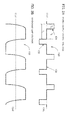
supply output voltage 130 shown inFIG. 2A , apositive voltage 134 and anegative voltage 136 are alternately output, and anoff time 132 is provided after each output of thepositive voltage 134 and thenegative voltage 136. The length of time to apply thepositive voltage 134 and thenegative voltage 136 is represented by ta, and the length of the off time is represented by tb. ta + tb = tc represents one period and is equal to the time from the application of the positive voltage to the application of the negative voltage. - By virtue of the power
supply output voltage 130 shown inFIG. 2A , the machining gap voltage between the wire electrode and the workpiece becomes a trapezoidal wave shapedvoltage 138 shown inFIG. 2B . - Next, the voltage change in a machining gap upon the occurrence of discharge in the machining gap will be described using
FIGS. 3A and 3B . -
FIG. 3A shows the machining gap voltage Vbb of a trapezoidal wave shapedvoltage 158 used in the present embodiment. Themachining gap voltages FIG. 3A . -
FIG. 3B shows the machining gap voltage Vbb of an AC high-frequency voltage 150 (used conventionally) shown inFIG. 11B . Themachining gap voltages FIG. 3B . - When the voltage is applied to the gap, the electrostatic attraction force acts between the wire electrode and the workpiece. And so, the wire electrode is bend toward the workpiece by the force, which degrades straightness accuracy. In general, the electrostatic attraction force is proportional to the square of the average gap voltage.
- In the machining gap voltage Vbb of the trapezoidal wave shaped
voltage 158 shown inFIG. 3A , compared with the machining gap voltage Vbb of the AC high-frequency voltage 150 shown inFIG. 3B , voltage reduction per one discharge is larger. Moreover, as a discharge frequency is increased, the electrostatic attraction force of the wire electrode is rapidly reduced, and straightness accuracy is improved. The offtimes voltage 158, whereby a discharge arc is reliably extinguished, and thus individual discharge positions are dispersed to hardly cause discharge concentration. If the concentration of the discharge points occurs, the surface roughness may be degraded. - In the usual AC high-frequency voltage used in the prior art (see,
FIGS. 11B and3B ), since an instantaneous value of the machining gap voltage Vbb is always changed, it is very difficult to determine the presence of discharge or the machining state from the change of voltage. In general, discharge often occurs near the peak value of the machining gap voltage Vbb. Although the machining gap voltage Vbb drops near the arc voltage at once due to discharge, after the peak of voltage, the voltage drops without discharge. Therefore, if the occurrence of discharge is slightly delayed, the difference between the voltage when discharge occurs and the voltage when discharge does not occur is reduced. Moreover, since the voltage changes at high speed, a slight deviation of determination timing may cause erroneous determination. Therefore, when the frequency is high in an AC high-frequency wave, it becomes virtually impossible to detect - Meanwhile, as in a trapezoidal wave shaped voltage used in the present embodiment (see,
FIGS. 2B and3A ), when the voltage application period is not more than 1 microsecond, after the power supply is turned off, a substantial amount of charge still remains in the stray capacitance C2 of themachining gap 7 before the next application of voltage. Therefore, if no discharge occurs, the machining gap voltage Vbb is maintained at approximately the peak value. Meanwhile, if discharge occurs, the machining gap voltage Vbb is maintained at not more than the arc voltage before the next voltage application. Therefore, a voltage change accompanying a change of the machining state is clear, and the change of the machining state can be accurately grasped by observing the machining gap voltage Vbb in the timing of starting the voltage application. - Hereinafter, means that determines the change of the machining state and is used in the embodiment of the present invention will be described. This means that determines the change of the machining state includes three-state discrimination signal output means (see,
FIG. 4 ), four-state discrimination signal output means (see,FIG. 6 ), and five-state discrimination signal output means (see,FIG. 8 ). - First, the three-state discrimination signal output means will be described with reference to
FIGS. 4 and5 . -
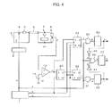
FIG. 4 is a view for explaining an embodiment of a wire cut electric discharge machine with the three-state discrimination signal output means.FIG. 5 is a timing chart showing the operation of the three-state discrimination signal output means shown inFIG. 4 . - The three-state discrimination signal output means shown in
FIG. 4 classifies the machining states into three states of "open", "discharge", and "short" and is constituted of acomparator 10, anSR latch 20, first and second D latches 22 and 23, and first, second, and thirdmonostable multi-vibrators comparator 10, theSR latch 20, the first and second D latches 22 and 23, and the first, second, and thirdmonostable multi-vibrators - As shown in
FIG. 4 , a voltageapplication timing generator 1 is a circuit that outputs a voltage application instruction 'a' for use in the driving of adriver circuit 2 that controls ON/OFF of aswitching element 4, outputs a latch instruction 'b' to theSR latch 20 and theD latch circuits D latch circuits - The voltage application instruction 'a' is output from the voltage
application timing generator 1 to drive the switchingelement 4 through thedriver circuit 2, and to apply a voltage to themachining gap 7. The machining gap voltage Vbb is divided into predetermined voltages by avoltage divider 8 to be input to thefirst comparator 10. A reference voltage V1 of thefirst comparator 10 is set to be not less than the arc voltage and not more than a power supply voltage E of theDC power supply 3. Specifically, since the machining gap voltage Vbb is divided into the predetermined voltages by thevoltage divider 8, the reference voltage V1 is set based on the values of the arc voltage and theDC power supply 3 corresponding to the division ratio. An output terminal of thefirst comparator circuit 10 is connected to an S terminal of thefirst SR latch 20 and a D terminal of thesecond D latch 23. - The
first D latch 22 receives an output signal 'i' from a Q terminal ofthefirstSRlatch20, the latch instruction 'b' and the reset instruction 'c' from the voltageapplication timing generator 1. Thesecond D latch 23 receives an output signal 'e' from thefirst comparator 10, the latch instruction 'b', and the reset instruction `c'. - A first AND
gate 30 receives an output signal 'f' from thesecond D latch 23 and the voltage application instruction `a' from the voltageapplication timing generator 1, and a second ANDgate 31 receives an output signal 'j' from thefirst D latch 22 and the voltage application instruction 'a' from the voltageapplication timing generator 1. - The first monostable multi-vibrator 50 receives an output signal 'g' from the first AND
gate 30 and outputs an output signal 'h' from the firstmonostable multi-vibrator 50. The third monostable multi-vibrator 52 receives an output signal 'k' from the second ANDgate 31 and outputs an output signal 'l' from the third monostable multi-vibrator52 . The output signals 'h' and 'l' respectively from the first and thirdmonostable multi-vibrators second inverters second inverters second inverters gate 36, and an output signal 'o' from the three-input ANDgate 36 is input to the secondmonostable multi-vibrator 51. The second monostable multi-vibrator 51 outputs an output signal 'p'. - The output signal 'h' is used as a signal (that is, an open signal 'h') for use in the determination of whether or not the
machining gap 7 is in an open state. The output signal 'p' is used as a signal (that is, a discharge signal 'p') for use in the determination of whether or not themachining gap 7 is in a discharge state. The output signal 'l' isusedasasignal (that is, a short signal 'l') for use in the determination of whether or not themachining gap 7 is in a short state. The open signal 'h', the discharge signal 'p', and the short signal 'l' are counted by a counting circuit (not shown). - Next, the operation of three-state discrimination signal output means will be described using
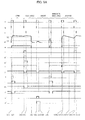
FIGS. 4 and5 . - As shown in a signal waveform 'a' of
FIG. 5 , when the voltageapplication timing generator 1 outputs the voltage application instruction 'a', thedriver circuit 2 is driven to control ON/OFF of the switching element 4 (see, 'a1'). When the switchingelement 4 is turned on by the voltage application instruction 'a' through thedriver circuit 2, the machining gap voltage Vbb is increased by theDC power supply 3. - When the output signal 'd' of the
voltage divider 8 is more than the reference voltage V1 of thefirst comparator 10, the output signal 'e' of thefirst comparator 10 is changed from low level to high level. Thefirst SR latch 20 is then set with the output signal 'e'. Consequently, a Q output 'i' of thefirst SR latch 20 is changed from low level to high level. The low and high levels respectively mean low and high potentials in an operating voltage of an electronic circuit. - If the voltage application instruction 'a' of the voltage
application timing generator 1 is returned to OFF (see, 'a2'), the charge accumulated in the stray capacitance C2 of themachining gap 7 remains. Therefore, the machining gap voltage Vbb is gradually reduced as long as no discharge occurs in themachining gap 7, and the output signals 'd', 'e', and 'i' are not changed. - Thereafter, the latch instruction 'b' is output from the voltage
application timing generator 1 to thefirst SR latch 20, thefirst D latch 22, and thesecond D latch 23 immediately before the next voltage application instruction 'a' (see, 'a3'). The latch instruction 'b' is input to a reset terminal of thefirst SR latch 20, a CK terminal of thefirst D latch 22, and a CK terminal of thesecond D latch 23. According to this constitution, the output 'e' of thefirst comparator 10 is held in thesecond D latch 23, and the output 'i' of thefirst SR latch 20 is held in thefirst D latch 22. Moreover, the output signal 'j' of a *Q terminal of thefirst D latch 22 is changed from high level to low level, and, at the same time, thefirst SR latch 20 is reset. Although the output 'i' of thefirst SR latch 20 is temporarily dropped to a low level, the output 'e' of thefirst comparator 10 is kept in a high level state, and therefore the output 'i' of thefirst SR latch 20 is immediately set to return to a high level. - The next moment, when the voltage application instruction 'a' of the voltage
application timing generator 1 reaches a high level (see, 'a3'), the output `f' of thesecond D latch 23 is also high level. Therefore, the output 'g' of the first ANDgate 30 is also high level to trigger the first monostable multi-vibrator 50, and to output the open signal 'h'. Meanwhile, since the output signal 'j' of the *Q terminal of thefirst D latch 22 is low level, the output signal 'k' of the second ANDgate 31 is held at a low level, and the short signal 'l' is not output from the third monostable multi-vibrator 52 (namely, the short signal 'l' is held at a low level). - Since the open signal 'h' from the secondmonostable multi-vibrator 51 reaches a high level, the input 'm' of the three-input AND
gate 36 is dropped to a low level. The output 'o' is held at a low level. The second monostable multi-vibrator 51 is thus not triggered, and the discharge signal 'p' is not output from the secondmonostable multi-vibrator 51. - The reset instruction 'c' is then output simultaneously with OFF of the voltage application instruction 'a' from the voltage application timing generator 1 (see, 'a4'), and the first and second D latches 22 and 23 are reset. The output 'j' of the *Q terminal of the
first D latch 22 is returned to a high level, and the output 'f' of the Q terminal of thesecond D latch 23 is returned to a low level. - Subsequently, when discharge occurs in the
machining gap 7, the machining gap voltage Vbb drops near the arc voltage at once (see, 'd1'), and the output 'e' of thefirst comparator 10 is returned to a low level. At that time, since the switchingelement 4 is already turned off, the voltage does not increase even if the discharge is terminated, and the machining gap voltage Vbb is kept at not more than the arc voltage. - Thereafter, when the latch instruction 'b' is output immediately before the next voltage application instruction 'a' from the voltage application timing generator 1 (see, 'a5'), the output 'e' of the
first comparator 10 is low level, and therefore, the Q output 'f' of thesecond D latch 23 is also low level. Meanwhile, since the output 'i' of thefirst SR latch 20 is held at a high level, the output signal 'j' of the *Q terminal of thefirst D latch 22 is dropped to a low level as in the previous time. - When the voltage application instruction 'a' then reaches a high level (see, 'a5'), the output signal 'f' of the Q terminal of the
second D latch 23 and the output signal 'j' of the *Q terminal of thefirst D latch 22 are low level this time. Therefore, since the output 'g' of the first ANDgate 30 and the output signal 'k' of the second ANDgate 31 are low level, the open signal 'h' from the first monostable multi-vibrator 50 and the short signal 'l' from the third monostable multi-vibrator 52 are not output. - On the other hand, the open signal 'h' and the short signal 'l' are input respectively to the
inverters gate 36 is high level to trigger the second monostable multi-vibrator 51, and to output the discharge signal 'p'. - Subsequently, the
machining gap 7 is in a short state, and when the output 'd' of thevoltage divider 8 is less than the reference voltage V1 of thefirst comparator 10, thefirst SR latch 20 is not set, and the output signal 'i' is held at a low level. In that case, the output 'j' of the *Q terminal of thefirst D latch 22 is held at a high level and is not changed. Moreover, since the output signal `f' of the Q terminal of thesecond D latch 23 is low level, only the output 'k' of the second ANDgate 31 is high level (see, 'k1'), and the short signal 'l' is output from the third monostable multi-vibrator 52 (see, `11'). - Next, four-state discrimination signal output means will be described with reference to
FIGS. 6 ,7A , and7B . -
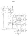
FIG. 6 is a view for explaining an embodiment of a wire cut electric discharge machine with the four-state discrimination signal outputmeans.FIGS. 7A and7B are timing charts showing the operation of the four-state discrimination signal output means shown inFIG. 6 . - Regarding the three states of "open", "discharge", and "short" obtained by the classification by the three-state discrimination signal output means shown in
FIG. 4 , the four-state discrimination signal output means shown inFIG. 6 classifies the "discharge" state in more detail into "discharge" and "immediate discharge", whereby the entire machining state is classified into four states of "open", "discharge", "immediate discharge", and "short". - The four-state discrimination signal output means shown in
FIG. 6 includes the components of the three-state discrimination signal output means shown inFIG. 4 , asecond comparator 12, asecond SR latch 21, athird D latch 24, a four-input ANDgate 33, a fourth monostable multi-vibrator 53, and a fifth monostable multi-vibrator 54. Moreover, the four-state discrimination signal output means uses a three-input ANDgate 32 instead of the three-input ANDgate 36, uses the fourth monostable multi-vibrator 53 instead of the second monostable multi-vibrator 51, and includes athird inverter 42 added as an input of the four-input ANDgate 33 inputting the signal to the fifth monostable multi-vibrator 54. - The voltage application instruction 'a' is output from the voltage
application timing generator 1 to drive the switchingelement 4 through thedriver circuit 2, and thus a voltage based on the power supply voltage E of theDC power supply 3 is applied to themachining gap 7. The machining gap voltage Vbb is divided into predetermined voltages by thevoltage divider 8 to be input to the first andsecond comparators first comparator 10 is set to be not less than the arc voltage, and a reference voltage V2 of thesecond comparator 12 is set to a value lower than the power supply voltage E and considering the voltage drop of the machining gap voltage Vbb during the off time (see,FIG. 2A ). Since the machining gap voltage Vbb is divided into the predetermined voltages by thevoltage divider 8, the reference voltages V1 and V2 are set based on values corresponding to the division ratio. - The machining gap voltage Vbb is increased, and when the output signal 'd' of the
voltage divider 8 is more than the reference voltage V1 of thefirst comparator 10, the output signal 'e' of thefirst comparator 10 is changed from low level to high level. Thefirst SR latch 20 is then set with the output signal 'e'. Consequently, the output signal 'i' of the Q terminal of thefirst SR latch 20 is changed from low level to high level. Moreover, the machining gap voltage Vbb is increased, and when the output signal 'd' of thevoltage divider 8 is more than the reference voltage V2 of thesecond comparator 12, an output signal 'q' of thesecond comparator 12 is changed from low level to high level, and likewise, thesecond SR latch 21 is set. Consequently, an output signal 'r' of a Q terminal of thesecond SR latch 21 is changed from low level to high level. - If the voltage application instruction 'a' from the voltage
application timing generator 1 is returned to OFF, the charge accumulated in the stray capacitance C2 of themachining gap 7 remains. Therefore, the machining gap voltage Vbb is gradually reduced as long as no discharge occurs, and the output signals 'e', 'i', 'q', and 'r' are not changed. - Thereafter, when the latch instruction 'b' is output from the voltage
application timing generator 1 immediately before the next voltage application instruction 'a', the output signal 'e' of thefirst comparator 10 is held in thesecond D latch 23, and the output signal 'i' of the Q terminal of thefirst SR latch 20 is held in thefirst D latch 22. Moreover, the output signal 'j' of the *Q terminal of thefirst D latch 22 is changed from high level to low level, and, at the same time, thefirst SR latch 20 is reset. According to this constitution, although the output signal 'i' of the Q terminal of thefirst SR latch 20 is temporarily dropped to a low level, the output of thefirst comparator 10 is held at a high level, and therefore the output signal 'i' of thefirst SR latch 20 is immediately set to return to a high level. Likewise, the output signal 'r' of the Q terminal of thesecond SR latch 21 is held in thethird D latch 24, and, at the same time, thesecond SR latch 21 is reset; however, since the output of thesecond comparator 12 is held at a high level, the output signal 'r' is immediately set again. - The next moment, when the voltage application instruction 'a' reaches a high level, the output signal 'f' of the Q terminal of the
second D latch 23 is also high level, and therefore, the output signal 'g' of the first ANDgate 30 is also high level. The output signal 'g' triggers the first monostable multi-vibrator 50 to output the open signal 'h'. Meanwhile, since the output signal 't' of a *Q terminal of thesecond D latch 23 is low level, the output signal 'o'' of the three-input ANDgate 32 is low level, and consequently, a discharge signal 'p'' is not output from thefourthmonostable multi-vibrator 53. Since the output signal 'j' of the *Q terminal of thefirst D latch 22 is low level, the output signal 'k' of the second ANDgate 31 is held at a low level, and the short signal '1' is not output from the thirdmonos table multi-vibrator 52. - Moreover, since the open signal 'h' is high level, the inversion signal 'm' is low level. The output signal 'v' of the four-input AND
gate 33 is held at a low level, and an immediate discharge signal 'w' is not output from the fifth monostable multi-vibrator 54. The reset instruction 'c' is then output simultaneously with OFF of the voltage application instruction 'a' from the voltageapplication timing generator 1, and the first, second, and third D latches 22, 23, and 24 are reset. The output signal `j' of the *Q terminal of thefirst D latch 22 is returned to a high level, the output signal 'f' of the Q terminal of thesecond D latch 23 is returned to a low level, the output signal 't' of the *Q terminal is returned to a high level, and the output signal 's' of the Q terminal of thethird D latch 24 is returned to a low level. - Subsequently, when discharge occurs in the
machining gap 7, the machining gap voltage Vbb drops near the arc voltage at once, and the output signal 'e' of thefirst comparator 10 and the output signal 'q' of thesecond comparator 12 are returned to low levels. At that time, since the switchingelement 4 is already turned off, the voltage does not increase even if the discharge is terminated, and the machining gap voltage Vbb is kept at not more than the arc voltage. Thereafter, when the latch instruction 'b' is output immediately before the next voltage application instruction 'a' , the output signal 'e' of thefirst comparator 10 is low level; therefore, the output signal 'f' of the Q terminal of thesecond D latch 23 is low level, and the output signal 't' of the *Q terminal is high level. Meanwhile, since the output signal 'i' of thefirst SR latch 20 and the output signal 'r' of thesecond SR latch 21 are held at a high level, the output signal 'j' of the *Q terminal of thefirst D latch 22 is low level, and the output signal 's' of the Q terminal of thethird D latch 24 is high level. - When the voltage application instruction 'a' then reaches a high level, the output signal 'f' from the Q terminal of the
second D latch 23 and the output signal 'j' from the *Q terminal of thefirst D latch 22 are low level this time. Meanwhile, the output signals' from the Q terminal of thethird D latch 24 and the output signal 't' from the *Q terminal of thesecond D latch 23 are high level. Therefore, the output signal 'g' of the first ANDgate 30 and the output signal 'k' of the second ANDgate 31 are low level, and only the output signal 'o'' of the three-input ANDgate 32 is high level. The discharge signal 'p'' is output from the fourth monostable multi-vibrator 53. - Subsequently, the
machining gap 7 is in a short state, and when the output signal 'd' of thevoltage divider 8 is less than the reference voltage V1 of thefirst comparator 10, the output signals 'e' and 'q' from the first andsecond comparators first D latch 22 and only the output signal 't' of the *Q terminal of thesecond D latch 23 are high level. Thus, when the voltage application instruction 'a' is high level, only the output signal 'k' of the second ANDgate 31 is high level, and the short signal 'l' is output. - Moreover, by virtue of the application of voltage, the output signal 'd' of the
voltage divider 8 is more than the reference voltage V1 of thefirst comparator 10, and thefirst SR latch 20 is set. Thereafter, when discharge occurs before reaching the reference voltage V2 of thesecond comparator 12, eventually only the output signal 't' of the *Q terminal of thesecond D latch 23 is high level. Therefore, the output signals 'g', 'k', and 'o'' of the first, second, and third ANDgates thirdmonostable multi-vibrators gate 33 is high level, and the immediate discharge signal 'w' is output from the fifth monostable multi-vibrator 54. - Next, five state discrimination signal output means will be described with reference to
FIGS. 8 ,9A , and9B . -
FIG. 8 is a view for explaining an embodiment of a wire cut electric discharge machine with the five-state discrimination signal output means.FIGS. 9A and9B are timing charts showing the operation of the five-state discrimination signal output means shown inFIG. 8 . - The five-state discrimination signal output means shown in
FIG. 8 uses afourth D latch 25, an ANDgate 38, and a seventh monostable multi-vibrator 56 instead of thesecond D latch 23, the first ANDgate 30, and the firstmonostable multi-vibrator 50 of the four-state discrimination signal output means shown inFIG. 6 . The five-state discrimination signal output means further includes a three-input ANDgate 37 and an eighthmonostable multi-vibrator 57. Moreover, the five-state discrimination signal output means uses a five-input ANDgate 35 and a ninth monostable multi-vibrator 58 instead of the four-input ANDgate 33 and the fifthmonostable multi-vibrator 54 ofFIG. 6 . Namely, compared with the four-state discrimination signal output means ofFIG. 6 , in the five-state discrimination signal output means ofFIG. 8 , thefourth D latch 25 holding the output signal 'q' of thesecond comparator 12 and a leakage signal output circuit are added, and the open discrimination circuit is changed; however, the other discrimination outputs are the same as those of the four-state discrimination signal output means. Namely, the output signal 'h'' represents an open state, 'p'' represents a discharge state, 'α' represents a leakage state, 'l' represents a short state, and 'w'' represents an immediate discharge state. Thus, with regard to the five-state discrimination signal output means, only an open state signal and a leakage state signal will be described. - The switching
element 4 is turned on based on the voltage application instruction 'a' from the voltageapplication timing generator 1, the machining gap voltage Vbb is increased, and the output signal 'd' of thevoltage divider 8 is more than the respective levels of the reference voltages V1 and V2 of the first andsecond comparators first SR latch 20 and the output signal 'r' from thesecond SR latch 21 are high level. - When that state is maintained until the next voltage application without occurrence of discharge, all D latches including the first to fourth D latches 22 to 25 set a high level signal by the output of the latch instruction 'b' immediately before the application instruction from the voltage application instruction 'a' from the voltage
application timing generator 1. Consequently, the output signals 'f' , 's', and 'x' of the Q terminals of the second, third, and fourth D latches 23, 24, and 25 are high levels, and the output signals 'j', 't', and 'y' of the *Q terminals of the first, second, and fourth D latches 22, 23, and, 25 are low levels. Therefore, when the voltage application instruction 'a' is high level, only the output signal 'g'' of the ANDgate 38 is high level, and the open signal 'h'' is output from the seventh monostable multi-vibrator 56. - Next, such a case is considered that the output signal 'd' from the
voltage divider 8 is more than the respective levels of the reference voltages V1 and V2 of the first andsecond comparators machining gap 7, the output signal 'd' is then gradually reduced, and when the next latch instruction 'b' is output, the output signal 'd' is reduced to not more than the level of the reference voltage V2. The first and second SR latches 20 and 21 are set, and since the output signal 'e' of thefirst comparator 10 is high level, the first, second, and third D latches 22, 23, and 24 set a high level signal. However, since the output signal 'q' of thesecond comparator 12 is low level, only thefourth D latch 25 sets a low level signal. - Consequently, the output signal 'f' of the Q terminal of the
second D latch 23, the output signal 's' of the Q terminal of thethird D latch 24, and the output signal 'y' of the *Q terminal of thefourth D latch 25 are high level. Meanwhile, the output signal 'j' of the *Q terminal of thefirst D latch 22, the output signal 't' of the *Q terminal of thesecond D latche 23, and the output signal 'x' of the *Q terminal of thefourth D latch 25 are low level. When the voltage application instruction 'a' is high level, only the output signal 'z' of the ANDgate 37 is high level, and the leakage signal 'α' is output from the eighth monostable multi-vibrator 57 this time. - Moreover, such a case is considered that although the output signal 'd' of the
voltage divider 8 is more than the reference voltage V1 of thefirst comparator 10 by virtue of the application of voltage to themachining gap 7, it does not reaches the reference voltage V2 of thesecond comparator 12, and the next latch instruction 'b' is output while this state is maintained (in other words, a case in which the output signal 'd' is maintained between the reference values V1 and V2). In that case, thefirst SR latch 20 is set, and since the output signal 'e' of thefirst comparator 10 is high level, the first and second D latches 22 and 23 set a high level signal. However, thesecond SR latch 21 is not set, and since the output signal 'q' of thesecond comparator 12 is low level, the third and fourth D latches 24 and 25 set a low level signal. - Consequently, the output signal 'f' of the Q terminal of the
second D latch 23 and the output signal 'y' of the *Q terminal of thefourth D latch 25 are high level, and the output signal 'j' of the Q terminal of thefirst D latch 22, the output signal 's' of the Q terminal of thethird D latch 24, the output signal 't' of the *Q terminal of thesecond D latch 23, and the output signal 'x' of the Q terminal of thefourth D latch 25 are low level. When the voltage application instruction 'a' is high level, only the output signal 'z' of the ANDgate 37 is high level again, and the leakage signal 'α' is output from theeighthmonostable multi-vibrator 57. -
FIG. 10 is a block diagram of the relevant portion of a controller of the wire cut electric discharge machine in one embodiment of the present invention. - As shown in
FIG. 10 , acontroller 80 includes aCPU 81, and amemory 82 constituted of a ROM and a RAM, adisplay 83,input device 84 such as a keyboard, aninterface 85 which inputs or outputs a machining program and so on from an external storage medium, respective axe control means 86, machining fluid flow rate control means 88 that controls the flow rate of a machining fluid, and apower circuit 98, which are connected to theCPU 81 through abus 89. A guide position of a work table and a wire electrode is controlled by the respective axes control means 86, and consequently, the position and speed of the wire electrode relative to the work table are determined. - The
power circuit 98 has been described usingFIGS. 4 ,6 , and8 and includes a voltage application circuit that applies voltage to a machining gap, a various-state detection circuit, and a counting circuit. - The respective axes control means 86 controls motors respectively driving X, Y, Z, U, and V axes and includes feedback control means for the position of each axis (X, Y, Z, U, and V axes), the speed, and the current. In the X and Y axes, a table (not shown) on which the
workpiece 7B (see,FIG. 1 ) is placed is driven in X-axis and Y-axis directions perpendicular to each other. In the Z axis, an upper guide is moved in a direction perpendicular to the X and Y axes. The U and V axes are used for taper machining and perpendicular to each other. The respective axes control means 86 is connected to aservo motor 94 for each axis through aservo amp 90 for each axis. Theservomotors 94 each include a position/speed detector, so that position and speed are fed back to respective axis control circuits. However, the description about the feedback is omitted inFIG. 10 . - The
power circuit 98 transmits to thecontroller 80 results obtained by counting three-state discrimination signals, four-state discrimination signals, or five-state discrimination signals for a predetermined time by means of the counting circuit. In thecontroller 80, based on the counting result of each state transmitted from thepower circuit 98, the counting is performed for a longer time if necessary to detect a trend in each state, and to obtain state discrimination data. Thecontroller 80 compares the state discrimination data with previously-set reference data to thereby control a relative feed speed of thewire electrode 7A with respect to theworkpiece 7B, control the off time of the power supply voltage, regulate the flow rate of the machining fluid, and change a set value of the positive and negative power supply voltages. - As described above, by virtue of the classification of the machining states, the machining state of the
machining gap 7 can be analogized more directly and in more detail than the prior art using an average voltage. For example, even when the leakage state, number of times of discharging, or number of times of short is increased, the average voltage drops. Thus, although it is hard to determine what are the reasons from the average voltage, the reason can be clearly determined in the case of the present invention, and a suitable response can be given as described later. However, the state is frequently shifted during machining due to the influences of a vibration state of a wire and a retention state of machining sludge, and therefore, if the machining state is tobe directly controlled based on individual results obtained for each voltage application, a system is vibrated to easily lose stability. Thus, it is empirically found that the machining state can be controlled better byperforming a control operation based on a number of results, for example, several tens to several hundreds of results. - The examples of the control operations will be shown as follows:
- ·When the ratio of the "open state" is increased, it is analogized that the discharge gap is increased, and thus, the feed speed of the wire electrode is increased, or the off time is prolonged, whereby the machining amount per unit distance is reduced;
- ·When the "short state" is increased, on the other hand, it is analogized that the machining gap is reduced, and therefore, the feed speed of the wire electrode is reduced, and, at the same time, the off time is reduced, or the power supply voltage is increased, whereby the machining amount per unit time is increased;
- ·When the "leakage state" is increased, machining sludge are highly likely to be retained, and therefore, intensity of machining fluid is increased to facilitate discharge of the machining sludge;
- ·When the ratio of the "immediate discharge state" is increased, it is analogized that the likelihood of shifting to the "short state" is increased, and therefore, a measure upon the "short" is taken early;
- ·As an alternate way, the feed speed is controlled so that the ratio of the "discharge state" is always constant, whereby stable machining may be maintained.
Claims (7)
- A wire cut electric discharge machine, which applies a high-frequency voltage to a machining gap between a wire electrode and a workpiece, disposed at a predetermined interval from the wire electrode, to produce discharge, and to machine the workpiece, comprising:voltage application means that applies a voltage having positive and negative polarities to the machining gap with a period of not more than 1 microsecond so that an off time of at least not less than the application time is provided between individual voltage applications;machining gap voltage detection means that detects a machining gap voltage generated in the machining gap;discrimination signal output means that, based on the machining gap voltage detected by the machining gap voltage detection means, classifies machining states into three states of "open", "discharge", and "short" for each voltage application performed by the voltage application means and outputs a state discrimination signal corresponding to each of the states; andcounting means that counts each of the state discrimination signals output from the discrimination signal output means to obtain state discrimination data.
- The wire cut electric discharge machine according to claim 1, wherein the discrimination signal output means has a discrimination level whose absolute value is not more than a no-load voltage and not less than an arc voltage, and in the timing of starting the voltage application to the machining gap,
the discrimination signal output means outputs an "open" signal when the absolute value of the machining gap voltage is not less than the discrimination level,
the discrimination signal output means outputs a "short" signal when the absolute value has never exceeded the discrimination level since the start of the last voltage application, and
the discrimination signal output means outputs a "discharge" signal in cases not corresponding to any of the above cases. - A wire cut electric discharge machine according to claim 1, wherein the discrimination signal output means is operable to classify machining states into four states of "open", "discharge", "immediate discharge", and "short" for each voltage application performed by the voltage application means.
- The wire cut electric discharge machine according to claim 3, wherein the discrimination signal output means has two discrimination levels including high and low levels whose absolute value is not more than a no-load voltage and not less than an arc voltage, and in the timing of starting the voltage application to the machining gap,
the discrimination signal output means outputs an "open" signal when the absolute value of the machining gap voltage is not less than the high level,
the discrimination signal output means outputs a "short" signal when the absolute value has never exceeded the low level since the start of the last voltage application,
the discrimination signal output means outputs a "discharge" signal when the absolute value has once exceeded the high level and is not more than the low level at the time of the next voltage application since the start of the last voltage application, and
the discrimination signal output means outputs an "immediate discharge" signal in cases not corresponding to any of the above cases. - A wire cut electric discharge machine according to claim 1, wherein the discrimination signal output means is operable to classify machining states into five states of "open", "leakage", "discharge", "immediate discharge", and "short" for each voltage application performed by the voltage application means.
- The wire cut electric discharge machine according to claim 5, wherein the discrimination signal output means has two discrimination levels including high and low levels whose absolute value is not more than a no-load voltage and not less than an arc voltage, and in the timing of starting the voltage application to the machining gap,
the discrimination signal output means outputs an "open" signal when the absolute value of the machining gap voltage is not less than the high level,
the discrimination signal output means outputs a "leakage" signal when the machining gap voltage is not more than the high level and not less than the low level,
the discrimination signal output means outputs a "short" signal when the absolute value has never exceeded the low level since the start of the last voltage application,
the discrimination signal output means outputs a "discharge" signal when the absolute value has once exceeded the high level and is not more than the low level at the time of the next voltage application since the start of the last voltage application, and
the discrimination signal output means outputs an "immediate discharge" signal in cases not corresponding to any of the above cases. - The wire cut electric discharge machine according to any one of claims 1, 3, and 5, wherein at least one value of the state discrimination data obtained by the counting means and a previously-set reference value are compared with each other, and at least one of the feed speed of the wire electrode, the length of the off time, the flow rate of a machining fluid, and a positive and negative power supply voltage set value of the voltage application means is changed.
Applications Claiming Priority (1)
| Application Number | Priority Date | Filing Date | Title |
|---|---|---|---|
| JP2009136605A JP4648468B2 (en) | 2009-06-05 | 2009-06-05 | Wire-cut electrical discharge machine with machining status judgment function |
Publications (3)
| Publication Number | Publication Date |
|---|---|
| EP2269755A2 true EP2269755A2 (en) | 2011-01-05 |
| EP2269755A3 EP2269755A3 (en) | 2012-10-10 |
| EP2269755B1 EP2269755B1 (en) | 2014-06-25 |
Family
ID=43126954
Family Applications (1)
| Application Number | Title | Priority Date | Filing Date |
|---|---|---|---|
| EP10164081.1A Active EP2269755B1 (en) | 2009-06-05 | 2010-05-27 | Wire cut electric discharge machine with machining state discrimination function |
Country Status (4)
| Country | Link |
|---|---|
| EP (1) | EP2269755B1 (en) |
| JP (1) | JP4648468B2 (en) |
| CN (1) | CN101905360B (en) |
| TW (1) | TWI436843B (en) |
Cited By (7)
| Publication number | Priority date | Publication date | Assignee | Title |
|---|---|---|---|---|
| EP2581162A1 (en) * | 2011-10-13 | 2013-04-17 | Fanuc Corporation | Wire electrical discharge machine that adjusts flow rate of working fluid based on machining state |
| US8735762B2 (en) | 2012-02-01 | 2014-05-27 | Fanuc Corporation | Wire electric discharge machine capable of detecting machining state and determining average voltage in machining gap |
| EP2752266A3 (en) * | 2013-01-08 | 2014-10-29 | Fanuc Corporation | Power supply device for electric discharge machining |
| EP2829348A3 (en) * | 2013-07-24 | 2015-02-11 | Fanuc Corporation | Wire electric discharge machine including average discharge delay time calculating unit |
| EP3135416A1 (en) * | 2015-08-25 | 2017-03-01 | Fanuc Corporation | Wire electric discharge machine operating with constant inter-pole distance |
| US9950378B2 (en) | 2015-04-02 | 2018-04-24 | Fanuc Corporation | Wire electric discharge machine |
| CN114131124A (en) * | 2020-09-03 | 2022-03-04 | 株式会社沙迪克 | Electric discharge machine |
Families Citing this family (12)
| Publication number | Priority date | Publication date | Assignee | Title |
|---|---|---|---|---|
| CN102601472B (en) * | 2011-01-19 | 2015-08-26 | 通用电气公司 | Electrical discharge machining system and method |
| CN103240474B (en) * | 2012-02-13 | 2018-07-10 | 严政 | A kind of spark erosion equipment discharging gap control method |
| CN102890220A (en) * | 2012-07-05 | 2013-01-23 | 宁波虎兴数控科技有限公司 | System for online test of linear cutting machine |
| JP5930913B2 (en) * | 2012-08-10 | 2016-06-08 | 三菱電機株式会社 | Wire electrical discharge machine |
| CN103962659B (en) * | 2014-05-13 | 2017-02-15 | 东莞华中科技大学制造工程研究院 | Method for electric spark machining control |
| JP6230481B2 (en) * | 2014-05-15 | 2017-11-15 | 三菱電機株式会社 | Multi-wire electric discharge machine |
| JP6063068B2 (en) * | 2015-04-02 | 2017-01-18 | ファナック株式会社 | Wire electric discharge machine |
| JP6426770B2 (en) * | 2017-02-06 | 2018-11-21 | ファナック株式会社 | Servo controller |
| CN107322109B (en) * | 2017-08-17 | 2023-04-25 | 江苏冬庆数控机床有限公司 | Circuit and method for inhibiting/eliminating flanging of orifice of electric spark perforation processing surface |
| JP6945489B2 (en) * | 2018-04-27 | 2021-10-06 | 三菱電機株式会社 | Multi-wire electric discharge machine |
| CN109202192B (en) * | 2018-10-31 | 2019-09-17 | 清华大学 | Fine electric spark servo scanning machined parameters preferred method and system |
| CN115156648B (en) * | 2022-07-15 | 2024-10-11 | 歌尔股份有限公司 | Mold processing method, apparatus, and computer-readable storage medium |
Citations (3)
| Publication number | Priority date | Publication date | Assignee | Title |
|---|---|---|---|---|
| JPS61260915A (en) | 1985-05-15 | 1986-11-19 | Mitsubishi Electric Corp | Power source for electric discharge machining |
| JP2002254250A (en) | 2000-12-25 | 2002-09-10 | Fanuc Ltd | Control unit for wire electric discharge machine |
| WO2004022275A1 (en) | 2002-08-30 | 2004-03-18 | Mitsubishi Denki Kabushiki Kaisha | Wire electric discharge machine |
Family Cites Families (14)
| Publication number | Priority date | Publication date | Assignee | Title |
|---|---|---|---|---|
| US3705286A (en) * | 1971-01-21 | 1972-12-05 | Iwao Kondo | Electric discharge machining device |
| JPS5596228A (en) * | 1979-01-08 | 1980-07-22 | Hitachi Seiko Ltd | Discharge working method |
| JPS5748424A (en) * | 1980-09-03 | 1982-03-19 | Hitachi Seiko Ltd | Control system for electric discharge machine |
| JPS59205223A (en) * | 1983-05-02 | 1984-11-20 | Mitsubishi Electric Corp | Electric discharge machining device |
| WO1989011371A1 (en) * | 1988-05-16 | 1989-11-30 | Charmilles Technologies Sa | Device and process for continuous adaptive control for an edm-wire cutting machine |
| JPH0475822A (en) * | 1990-07-12 | 1992-03-10 | I N R Kenkyusho:Kk | Electric discharge machining device |
| JP2939310B2 (en) * | 1990-08-14 | 1999-08-25 | 株式会社ソディック | Electric discharge machine |
| JP3293416B2 (en) * | 1994-08-09 | 2002-06-17 | 三菱電機株式会社 | Discharge state detection device for electric discharge machine |
| JPH0911043A (en) * | 1995-06-29 | 1997-01-14 | Nec Corp | Electric discharge machining method and electric discharge machining device |
| JP2000079514A (en) * | 1998-09-01 | 2000-03-21 | Mitsubishi Electric Corp | Electric discharge machine |
| JP3835452B2 (en) * | 2002-06-12 | 2006-10-18 | 三菱電機株式会社 | Machining power supply device for wire electric discharge machine |
| GB0504600D0 (en) * | 2005-03-04 | 2005-04-13 | Univ Strathclyde | Detecting partial discharge in high voltage cables |
| JP2007044813A (en) * | 2005-08-10 | 2007-02-22 | Fanuc Ltd | Electric discharge machining device |
| CN100427961C (en) * | 2006-09-20 | 2008-10-22 | 重庆大学 | On-line Monitoring Method of Gas Insulated Combined Electrical Apparatus Based on Virtual Instrument Technology |
-
2009
- 2009-06-05 JP JP2009136605A patent/JP4648468B2/en active Active
-
2010
- 2010-04-28 TW TW99113520A patent/TWI436843B/en active
- 2010-05-27 EP EP10164081.1A patent/EP2269755B1/en active Active
- 2010-06-04 CN CN2010101988443A patent/CN101905360B/en active Active
Patent Citations (3)
| Publication number | Priority date | Publication date | Assignee | Title |
|---|---|---|---|---|
| JPS61260915A (en) | 1985-05-15 | 1986-11-19 | Mitsubishi Electric Corp | Power source for electric discharge machining |
| JP2002254250A (en) | 2000-12-25 | 2002-09-10 | Fanuc Ltd | Control unit for wire electric discharge machine |
| WO2004022275A1 (en) | 2002-08-30 | 2004-03-18 | Mitsubishi Denki Kabushiki Kaisha | Wire electric discharge machine |
Cited By (13)
| Publication number | Priority date | Publication date | Assignee | Title |
|---|---|---|---|---|
| US8680422B2 (en) | 2011-10-13 | 2014-03-25 | Fanuc Corporation | Wire electrical discharge machine that adjusts flow rate of working fluid based on machining state |
| EP2581162A1 (en) * | 2011-10-13 | 2013-04-17 | Fanuc Corporation | Wire electrical discharge machine that adjusts flow rate of working fluid based on machining state |
| US8735762B2 (en) | 2012-02-01 | 2014-05-27 | Fanuc Corporation | Wire electric discharge machine capable of detecting machining state and determining average voltage in machining gap |
| EP2752266A3 (en) * | 2013-01-08 | 2014-10-29 | Fanuc Corporation | Power supply device for electric discharge machining |
| US9486869B2 (en) | 2013-01-08 | 2016-11-08 | Fanuc Corporation | Power supply device for electric discharge machining |
| US10543546B2 (en) | 2013-07-24 | 2020-01-28 | Fanuc Corporation | Wire electric discharge machine including average discharge delay time calculating unit |
| EP2829348A3 (en) * | 2013-07-24 | 2015-02-11 | Fanuc Corporation | Wire electric discharge machine including average discharge delay time calculating unit |
| US9833853B2 (en) | 2013-07-24 | 2017-12-05 | Fanuc Corporation | Wire electric discharge machine including average discharge delay time calculating unit |
| US10792744B2 (en) | 2013-07-24 | 2020-10-06 | Fanuc Corporation | Wire electric discharge machine including average discharge delay time calculating unit |
| US9950378B2 (en) | 2015-04-02 | 2018-04-24 | Fanuc Corporation | Wire electric discharge machine |
| EP3135416A1 (en) * | 2015-08-25 | 2017-03-01 | Fanuc Corporation | Wire electric discharge machine operating with constant inter-pole distance |
| US10315263B2 (en) | 2015-08-25 | 2019-06-11 | Fanuc Corporation | Wire electric discharge machine operating with constant inter-pole distance |
| CN114131124A (en) * | 2020-09-03 | 2022-03-04 | 株式会社沙迪克 | Electric discharge machine |
Also Published As
| Publication number | Publication date |
|---|---|
| JP2010280046A (en) | 2010-12-16 |
| TW201102199A (en) | 2011-01-16 |
| TWI436843B (en) | 2014-05-11 |
| EP2269755A3 (en) | 2012-10-10 |
| CN101905360A (en) | 2010-12-08 |
| JP4648468B2 (en) | 2011-03-09 |
| CN101905360B (en) | 2012-07-04 |
| EP2269755B1 (en) | 2014-06-25 |
Similar Documents
| Publication | Publication Date | Title |
|---|---|---|
| EP2269755B1 (en) | Wire cut electric discharge machine with machining state discrimination function | |
| JP5204321B1 (en) | Wire electrical discharge machine that detects the machining state and calculates the average voltage between the electrodes | |
| EP2505293B1 (en) | Wire electric discharge machine capable of detecting machining state | |
| JP5739563B2 (en) | Wire electric discharge machine equipped with means for calculating average discharge delay time | |
| EP2223764B1 (en) | Wire electric discharge machine | |
| US9272349B2 (en) | Numerical control device, wire electric discharge machining apparatus using the same, and wire electric discharge machining method using the same | |
| JP4833198B2 (en) | Power control device for electrical discharge machine | |
| JP4833197B2 (en) | Power control device for electrical discharge machine | |
| CN103909313B (en) | Electric discharge machining source apparatus | |
| JP5357298B2 (en) | Wire electrical discharge machine to detect machining status | |
| CN104837588B (en) | Electric discharge device | |
| CN104837588A (en) | Electrical discharge machining device |
Legal Events
| Date | Code | Title | Description |
|---|---|---|---|
| PUAI | Public reference made under article 153(3) epc to a published international application that has entered the european phase |
Free format text: ORIGINAL CODE: 0009012 |
|
| AK | Designated contracting states |
Kind code of ref document: A2 Designated state(s): AL AT BE BG CH CY CZ DE DK EE ES FI FR GB GR HR HU IE IS IT LI LT LU LV MC MK MT NL NO PL PT RO SE SI SK SM TR |
|
| AX | Request for extension of the european patent |
Extension state: BA ME RS |
|
| RAP1 | Party data changed (applicant data changed or rights of an application transferred) |
Owner name: FANUC CORPORATION |
|
| PUAL | Search report despatched |
Free format text: ORIGINAL CODE: 0009013 |
|
| AK | Designated contracting states |
Kind code of ref document: A3 Designated state(s): AL AT BE BG CH CY CZ DE DK EE ES FI FR GB GR HR HU IE IS IT LI LT LU LV MC MK MT NL NO PL PT RO SE SI SK SM TR |
|
| AX | Request for extension of the european patent |
Extension state: BA ME RS |
|
| RIC1 | Information provided on ipc code assigned before grant |
Ipc: B23H 1/02 20060101AFI20120831BHEP |
|
| 17P | Request for examination filed |
Effective date: 20130404 |
|
| 17Q | First examination report despatched |
Effective date: 20130530 |
|
| GRAP | Despatch of communication of intention to grant a patent |
Free format text: ORIGINAL CODE: EPIDOSNIGR1 |
|
| INTG | Intention to grant announced |
Effective date: 20140110 |
|
| GRAS | Grant fee paid |
Free format text: ORIGINAL CODE: EPIDOSNIGR3 |
|
| GRAA | (expected) grant |
Free format text: ORIGINAL CODE: 0009210 |
|
| AK | Designated contracting states |
Kind code of ref document: B1 Designated state(s): AL AT BE BG CH CY CZ DE DK EE ES FI FR GB GR HR HU IE IS IT LI LT LU LV MC MK MT NL NO PL PT RO SE SI SK SM TR |
|
| REG | Reference to a national code |
Ref country code: GB Ref legal event code: FG4D |
|
| REG | Reference to a national code |
Ref country code: CH Ref legal event code: EP |
|
| REG | Reference to a national code |
Ref country code: CH Ref legal event code: NV Representative=s name: DR. LUSUARDI AG, CH Ref country code: AT Ref legal event code: REF Ref document number: 674310 Country of ref document: AT Kind code of ref document: T Effective date: 20140715 |
|
| REG | Reference to a national code |
Ref country code: IE Ref legal event code: FG4D |
|
| REG | Reference to a national code |
Ref country code: DE Ref legal event code: R096 Ref document number: 602010016932 Country of ref document: DE Effective date: 20140731 |
|
| PG25 | Lapsed in a contracting state [announced via postgrant information from national office to epo] |
Ref country code: GR Free format text: LAPSE BECAUSE OF FAILURE TO SUBMIT A TRANSLATION OF THE DESCRIPTION OR TO PAY THE FEE WITHIN THE PRESCRIBED TIME-LIMIT Effective date: 20140926 Ref country code: NO Free format text: LAPSE BECAUSE OF FAILURE TO SUBMIT A TRANSLATION OF THE DESCRIPTION OR TO PAY THE FEE WITHIN THE PRESCRIBED TIME-LIMIT Effective date: 20140925 Ref country code: CY Free format text: LAPSE BECAUSE OF FAILURE TO SUBMIT A TRANSLATION OF THE DESCRIPTION OR TO PAY THE FEE WITHIN THE PRESCRIBED TIME-LIMIT Effective date: 20140625 Ref country code: FI Free format text: LAPSE BECAUSE OF FAILURE TO SUBMIT A TRANSLATION OF THE DESCRIPTION OR TO PAY THE FEE WITHIN THE PRESCRIBED TIME-LIMIT Effective date: 20140625 Ref country code: LT Free format text: LAPSE BECAUSE OF FAILURE TO SUBMIT A TRANSLATION OF THE DESCRIPTION OR TO PAY THE FEE WITHIN THE PRESCRIBED TIME-LIMIT Effective date: 20140625 |
|
| REG | Reference to a national code |
Ref country code: AT Ref legal event code: MK05 Ref document number: 674310 Country of ref document: AT Kind code of ref document: T Effective date: 20140625 |
|
| REG | Reference to a national code |
Ref country code: NL Ref legal event code: VDEP Effective date: 20140625 |
|
| REG | Reference to a national code |
Ref country code: LT Ref legal event code: MG4D |
|
| PG25 | Lapsed in a contracting state [announced via postgrant information from national office to epo] |
Ref country code: SE Free format text: LAPSE BECAUSE OF FAILURE TO SUBMIT A TRANSLATION OF THE DESCRIPTION OR TO PAY THE FEE WITHIN THE PRESCRIBED TIME-LIMIT Effective date: 20140625 Ref country code: LV Free format text: LAPSE BECAUSE OF FAILURE TO SUBMIT A TRANSLATION OF THE DESCRIPTION OR TO PAY THE FEE WITHIN THE PRESCRIBED TIME-LIMIT Effective date: 20140625 Ref country code: HR Free format text: LAPSE BECAUSE OF FAILURE TO SUBMIT A TRANSLATION OF THE DESCRIPTION OR TO PAY THE FEE WITHIN THE PRESCRIBED TIME-LIMIT Effective date: 20140625 |
|
| PG25 | Lapsed in a contracting state [announced via postgrant information from national office to epo] |
Ref country code: ES Free format text: LAPSE BECAUSE OF FAILURE TO SUBMIT A TRANSLATION OF THE DESCRIPTION OR TO PAY THE FEE WITHIN THE PRESCRIBED TIME-LIMIT Effective date: 20140625 Ref country code: CZ Free format text: LAPSE BECAUSE OF FAILURE TO SUBMIT A TRANSLATION OF THE DESCRIPTION OR TO PAY THE FEE WITHIN THE PRESCRIBED TIME-LIMIT Effective date: 20140625 Ref country code: RO Free format text: LAPSE BECAUSE OF FAILURE TO SUBMIT A TRANSLATION OF THE DESCRIPTION OR TO PAY THE FEE WITHIN THE PRESCRIBED TIME-LIMIT Effective date: 20140625 Ref country code: PT Free format text: LAPSE BECAUSE OF FAILURE TO SUBMIT A TRANSLATION OF THE DESCRIPTION OR TO PAY THE FEE WITHIN THE PRESCRIBED TIME-LIMIT Effective date: 20141027 Ref country code: SK Free format text: LAPSE BECAUSE OF FAILURE TO SUBMIT A TRANSLATION OF THE DESCRIPTION OR TO PAY THE FEE WITHIN THE PRESCRIBED TIME-LIMIT Effective date: 20140625 Ref country code: EE Free format text: LAPSE BECAUSE OF FAILURE TO SUBMIT A TRANSLATION OF THE DESCRIPTION OR TO PAY THE FEE WITHIN THE PRESCRIBED TIME-LIMIT Effective date: 20140625 |
|
| PG25 | Lapsed in a contracting state [announced via postgrant information from national office to epo] |
Ref country code: IS Free format text: LAPSE BECAUSE OF FAILURE TO SUBMIT A TRANSLATION OF THE DESCRIPTION OR TO PAY THE FEE WITHIN THE PRESCRIBED TIME-LIMIT Effective date: 20141025 Ref country code: NL Free format text: LAPSE BECAUSE OF FAILURE TO SUBMIT A TRANSLATION OF THE DESCRIPTION OR TO PAY THE FEE WITHIN THE PRESCRIBED TIME-LIMIT Effective date: 20140625 Ref country code: PL Free format text: LAPSE BECAUSE OF FAILURE TO SUBMIT A TRANSLATION OF THE DESCRIPTION OR TO PAY THE FEE WITHIN THE PRESCRIBED TIME-LIMIT Effective date: 20140625 Ref country code: AT Free format text: LAPSE BECAUSE OF FAILURE TO SUBMIT A TRANSLATION OF THE DESCRIPTION OR TO PAY THE FEE WITHIN THE PRESCRIBED TIME-LIMIT Effective date: 20140625 |
|
| REG | Reference to a national code |
Ref country code: DE Ref legal event code: R097 Ref document number: 602010016932 Country of ref document: DE |
|
| PG25 | Lapsed in a contracting state [announced via postgrant information from national office to epo] |
Ref country code: IT Free format text: LAPSE BECAUSE OF FAILURE TO SUBMIT A TRANSLATION OF THE DESCRIPTION OR TO PAY THE FEE WITHIN THE PRESCRIBED TIME-LIMIT Effective date: 20140625 Ref country code: DK Free format text: LAPSE BECAUSE OF FAILURE TO SUBMIT A TRANSLATION OF THE DESCRIPTION OR TO PAY THE FEE WITHIN THE PRESCRIBED TIME-LIMIT Effective date: 20140625 |
|
| PLBE | No opposition filed within time limit |
Free format text: ORIGINAL CODE: 0009261 |
|
| STAA | Information on the status of an ep patent application or granted ep patent |
Free format text: STATUS: NO OPPOSITION FILED WITHIN TIME LIMIT |
|
| 26N | No opposition filed |
Effective date: 20150326 |
|
| PG25 | Lapsed in a contracting state [announced via postgrant information from national office to epo] |
Ref country code: BE Free format text: LAPSE BECAUSE OF FAILURE TO SUBMIT A TRANSLATION OF THE DESCRIPTION OR TO PAY THE FEE WITHIN THE PRESCRIBED TIME-LIMIT Effective date: 20140625 |
|
| REG | Reference to a national code |
Ref country code: DE Ref legal event code: R097 Ref document number: 602010016932 Country of ref document: DE Effective date: 20150326 |
|
| PG25 | Lapsed in a contracting state [announced via postgrant information from national office to epo] |
Ref country code: SI Free format text: LAPSE BECAUSE OF FAILURE TO SUBMIT A TRANSLATION OF THE DESCRIPTION OR TO PAY THE FEE WITHIN THE PRESCRIBED TIME-LIMIT Effective date: 20140625 |
|
| GBPC | Gb: european patent ceased through non-payment of renewal fee |
Effective date: 20150527 |
|
| PG25 | Lapsed in a contracting state [announced via postgrant information from national office to epo] |
Ref country code: MC Free format text: LAPSE BECAUSE OF FAILURE TO SUBMIT A TRANSLATION OF THE DESCRIPTION OR TO PAY THE FEE WITHIN THE PRESCRIBED TIME-LIMIT Effective date: 20140625 Ref country code: LU Free format text: LAPSE BECAUSE OF FAILURE TO SUBMIT A TRANSLATION OF THE DESCRIPTION OR TO PAY THE FEE WITHIN THE PRESCRIBED TIME-LIMIT Effective date: 20150527 |
|
| REG | Reference to a national code |
Ref country code: IE Ref legal event code: MM4A |
|
| REG | Reference to a national code |
Ref country code: FR Ref legal event code: ST Effective date: 20160129 |
|
| PG25 | Lapsed in a contracting state [announced via postgrant information from national office to epo] |
Ref country code: GB Free format text: LAPSE BECAUSE OF NON-PAYMENT OF DUE FEES Effective date: 20150527 Ref country code: IE Free format text: LAPSE BECAUSE OF NON-PAYMENT OF DUE FEES Effective date: 20150527 |
|
| PG25 | Lapsed in a contracting state [announced via postgrant information from national office to epo] |
Ref country code: FR Free format text: LAPSE BECAUSE OF NON-PAYMENT OF DUE FEES Effective date: 20150601 |
|
| PG25 | Lapsed in a contracting state [announced via postgrant information from national office to epo] |
Ref country code: MT Free format text: LAPSE BECAUSE OF FAILURE TO SUBMIT A TRANSLATION OF THE DESCRIPTION OR TO PAY THE FEE WITHIN THE PRESCRIBED TIME-LIMIT Effective date: 20140625 |
|
| PG25 | Lapsed in a contracting state [announced via postgrant information from national office to epo] |
Ref country code: SM Free format text: LAPSE BECAUSE OF FAILURE TO SUBMIT A TRANSLATION OF THE DESCRIPTION OR TO PAY THE FEE WITHIN THE PRESCRIBED TIME-LIMIT Effective date: 20140625 Ref country code: BG Free format text: LAPSE BECAUSE OF FAILURE TO SUBMIT A TRANSLATION OF THE DESCRIPTION OR TO PAY THE FEE WITHIN THE PRESCRIBED TIME-LIMIT Effective date: 20140625 Ref country code: HU Free format text: LAPSE BECAUSE OF FAILURE TO SUBMIT A TRANSLATION OF THE DESCRIPTION OR TO PAY THE FEE WITHIN THE PRESCRIBED TIME-LIMIT; INVALID AB INITIO Effective date: 20100527 |
|
| PG25 | Lapsed in a contracting state [announced via postgrant information from national office to epo] |
Ref country code: TR Free format text: LAPSE BECAUSE OF FAILURE TO SUBMIT A TRANSLATION OF THE DESCRIPTION OR TO PAY THE FEE WITHIN THE PRESCRIBED TIME-LIMIT Effective date: 20140625 |
|
| PG25 | Lapsed in a contracting state [announced via postgrant information from national office to epo] |
Ref country code: MK Free format text: LAPSE BECAUSE OF FAILURE TO SUBMIT A TRANSLATION OF THE DESCRIPTION OR TO PAY THE FEE WITHIN THE PRESCRIBED TIME-LIMIT Effective date: 20140625 |
|
| PG25 | Lapsed in a contracting state [announced via postgrant information from national office to epo] |
Ref country code: AL Free format text: LAPSE BECAUSE OF FAILURE TO SUBMIT A TRANSLATION OF THE DESCRIPTION OR TO PAY THE FEE WITHIN THE PRESCRIBED TIME-LIMIT Effective date: 20140625 |
|
| REG | Reference to a national code |
Ref country code: DE Ref legal event code: R082 Ref document number: 602010016932 Country of ref document: DE Representative=s name: HL KEMPNER PATENTANWAELTE, SOLICITORS (ENGLAND, DE Ref country code: DE Ref legal event code: R082 Ref document number: 602010016932 Country of ref document: DE Representative=s name: HL KEMPNER PARTG MBB, DE Ref country code: DE Ref legal event code: R082 Ref document number: 602010016932 Country of ref document: DE Representative=s name: HL KEMPNER PATENTANWALT, RECHTSANWALT, SOLICIT, DE |
|
| PGFP | Annual fee paid to national office [announced via postgrant information from national office to epo] |
Ref country code: DE Payment date: 20250423 Year of fee payment: 16 |
|
| PGFP | Annual fee paid to national office [announced via postgrant information from national office to epo] |
Ref country code: CH Payment date: 20250601 Year of fee payment: 16 |