EP2267796A2 - Separation method of nitride semiconductor layer, semiconductor device, manufacturing method thereof, semiconductor wafer, and manufacturing method thereof - Google Patents
Separation method of nitride semiconductor layer, semiconductor device, manufacturing method thereof, semiconductor wafer, and manufacturing method thereof Download PDFInfo
- Publication number
- EP2267796A2 EP2267796A2 EP10167073A EP10167073A EP2267796A2 EP 2267796 A2 EP2267796 A2 EP 2267796A2 EP 10167073 A EP10167073 A EP 10167073A EP 10167073 A EP10167073 A EP 10167073A EP 2267796 A2 EP2267796 A2 EP 2267796A2
- Authority
- EP
- European Patent Office
- Prior art keywords
- layer
- nitride semiconductor
- substrate
- semiconductor layer
- graphene
- Prior art date
- Legal status (The legal status is an assumption and is not a legal conclusion. Google has not performed a legal analysis and makes no representation as to the accuracy of the status listed.)
- Withdrawn
Links
Images










Classifications
-
- H—ELECTRICITY
- H10—SEMICONDUCTOR DEVICES; ELECTRIC SOLID-STATE DEVICES NOT OTHERWISE PROVIDED FOR
- H10H—INORGANIC LIGHT-EMITTING SEMICONDUCTOR DEVICES HAVING POTENTIAL BARRIERS
- H10H20/00—Individual inorganic light-emitting semiconductor devices having potential barriers, e.g. light-emitting diodes [LED]
- H10H20/01—Manufacture or treatment
- H10H20/011—Manufacture or treatment of bodies, e.g. forming semiconductor layers
- H10H20/013—Manufacture or treatment of bodies, e.g. forming semiconductor layers having light-emitting regions comprising only Group III-V materials
- H10H20/0133—Manufacture or treatment of bodies, e.g. forming semiconductor layers having light-emitting regions comprising only Group III-V materials with a substrate not being Group III-V materials
- H10H20/01335—Manufacture or treatment of bodies, e.g. forming semiconductor layers having light-emitting regions comprising only Group III-V materials with a substrate not being Group III-V materials the light-emitting regions comprising nitride materials
-
- H—ELECTRICITY
- H10—SEMICONDUCTOR DEVICES; ELECTRIC SOLID-STATE DEVICES NOT OTHERWISE PROVIDED FOR
- H10D—INORGANIC ELECTRIC SEMICONDUCTOR DEVICES
- H10D62/00—Semiconductor bodies, or regions thereof, of devices having potential barriers
- H10D62/80—Semiconductor bodies, or regions thereof, of devices having potential barriers characterised by the materials
- H10D62/83—Semiconductor bodies, or regions thereof, of devices having potential barriers characterised by the materials being Group IV materials, e.g. B-doped Si or undoped Ge
-
- H—ELECTRICITY
- H10—SEMICONDUCTOR DEVICES; ELECTRIC SOLID-STATE DEVICES NOT OTHERWISE PROVIDED FOR
- H10D—INORGANIC ELECTRIC SEMICONDUCTOR DEVICES
- H10D62/00—Semiconductor bodies, or regions thereof, of devices having potential barriers
- H10D62/80—Semiconductor bodies, or regions thereof, of devices having potential barriers characterised by the materials
- H10D62/85—Semiconductor bodies, or regions thereof, of devices having potential barriers characterised by the materials being Group III-V materials, e.g. GaAs
- H10D62/8503—Nitride Group III-V materials, e.g. AlN or GaN
-
- H—ELECTRICITY
- H10—SEMICONDUCTOR DEVICES; ELECTRIC SOLID-STATE DEVICES NOT OTHERWISE PROVIDED FOR
- H10D—INORGANIC ELECTRIC SEMICONDUCTOR DEVICES
- H10D62/00—Semiconductor bodies, or regions thereof, of devices having potential barriers
- H10D62/80—Semiconductor bodies, or regions thereof, of devices having potential barriers characterised by the materials
- H10D62/881—Semiconductor bodies, or regions thereof, of devices having potential barriers characterised by the materials being a two-dimensional material
- H10D62/882—Graphene
-
- H—ELECTRICITY
- H10—SEMICONDUCTOR DEVICES; ELECTRIC SOLID-STATE DEVICES NOT OTHERWISE PROVIDED FOR
- H10H—INORGANIC LIGHT-EMITTING SEMICONDUCTOR DEVICES HAVING POTENTIAL BARRIERS
- H10H20/00—Individual inorganic light-emitting semiconductor devices having potential barriers, e.g. light-emitting diodes [LED]
- H10H20/01—Manufacture or treatment
- H10H20/011—Manufacture or treatment of bodies, e.g. forming semiconductor layers
- H10H20/018—Bonding of wafers
-
- H—ELECTRICITY
- H10—SEMICONDUCTOR DEVICES; ELECTRIC SOLID-STATE DEVICES NOT OTHERWISE PROVIDED FOR
- H10P—GENERIC PROCESSES OR APPARATUS FOR THE MANUFACTURE OR TREATMENT OF DEVICES COVERED BY CLASS H10
- H10P14/00—Formation of materials, e.g. in the shape of layers or pillars
- H10P14/20—Formation of materials, e.g. in the shape of layers or pillars of semiconductor materials
-
- H—ELECTRICITY
- H10—SEMICONDUCTOR DEVICES; ELECTRIC SOLID-STATE DEVICES NOT OTHERWISE PROVIDED FOR
- H10P—GENERIC PROCESSES OR APPARATUS FOR THE MANUFACTURE OR TREATMENT OF DEVICES COVERED BY CLASS H10
- H10P14/00—Formation of materials, e.g. in the shape of layers or pillars
- H10P14/20—Formation of materials, e.g. in the shape of layers or pillars of semiconductor materials
- H10P14/22—Formation of materials, e.g. in the shape of layers or pillars of semiconductor materials using physical deposition, e.g. vacuum deposition or sputtering
-
- H—ELECTRICITY
- H10—SEMICONDUCTOR DEVICES; ELECTRIC SOLID-STATE DEVICES NOT OTHERWISE PROVIDED FOR
- H10P—GENERIC PROCESSES OR APPARATUS FOR THE MANUFACTURE OR TREATMENT OF DEVICES COVERED BY CLASS H10
- H10P14/00—Formation of materials, e.g. in the shape of layers or pillars
- H10P14/20—Formation of materials, e.g. in the shape of layers or pillars of semiconductor materials
- H10P14/24—Formation of materials, e.g. in the shape of layers or pillars of semiconductor materials using chemical vapour deposition [CVD]
-
- H—ELECTRICITY
- H10—SEMICONDUCTOR DEVICES; ELECTRIC SOLID-STATE DEVICES NOT OTHERWISE PROVIDED FOR
- H10P—GENERIC PROCESSES OR APPARATUS FOR THE MANUFACTURE OR TREATMENT OF DEVICES COVERED BY CLASS H10
- H10P14/00—Formation of materials, e.g. in the shape of layers or pillars
- H10P14/20—Formation of materials, e.g. in the shape of layers or pillars of semiconductor materials
- H10P14/29—Formation of materials, e.g. in the shape of layers or pillars of semiconductor materials characterised by the substrates
- H10P14/2901—Materials
- H10P14/2902—Materials being Group IVA materials
- H10P14/2904—Silicon carbide
-
- H—ELECTRICITY
- H10—SEMICONDUCTOR DEVICES; ELECTRIC SOLID-STATE DEVICES NOT OTHERWISE PROVIDED FOR
- H10P—GENERIC PROCESSES OR APPARATUS FOR THE MANUFACTURE OR TREATMENT OF DEVICES COVERED BY CLASS H10
- H10P14/00—Formation of materials, e.g. in the shape of layers or pillars
- H10P14/20—Formation of materials, e.g. in the shape of layers or pillars of semiconductor materials
- H10P14/32—Formation of materials, e.g. in the shape of layers or pillars of semiconductor materials characterised by intermediate layers between substrates and deposited layers
- H10P14/3202—Materials thereof
- H10P14/3204—Materials thereof being Group IVA semiconducting materials
- H10P14/3206—Carbon, e.g. diamond-like carbon
-
- H—ELECTRICITY
- H10—SEMICONDUCTOR DEVICES; ELECTRIC SOLID-STATE DEVICES NOT OTHERWISE PROVIDED FOR
- H10P—GENERIC PROCESSES OR APPARATUS FOR THE MANUFACTURE OR TREATMENT OF DEVICES COVERED BY CLASS H10
- H10P14/00—Formation of materials, e.g. in the shape of layers or pillars
- H10P14/20—Formation of materials, e.g. in the shape of layers or pillars of semiconductor materials
- H10P14/34—Deposited materials, e.g. layers
- H10P14/3402—Deposited materials, e.g. layers characterised by the chemical composition
- H10P14/3414—Deposited materials, e.g. layers characterised by the chemical composition being group IIIA-VIA materials
- H10P14/3416—Nitrides
-
- H—ELECTRICITY
- H10—SEMICONDUCTOR DEVICES; ELECTRIC SOLID-STATE DEVICES NOT OTHERWISE PROVIDED FOR
- H10P—GENERIC PROCESSES OR APPARATUS FOR THE MANUFACTURE OR TREATMENT OF DEVICES COVERED BY CLASS H10
- H10P14/00—Formation of materials, e.g. in the shape of layers or pillars
- H10P14/20—Formation of materials, e.g. in the shape of layers or pillars of semiconductor materials
- H10P14/38—Formation of materials, e.g. in the shape of layers or pillars of semiconductor materials characterised by treatments done after the formation of the materials
Definitions
- the present invention relates to a separation method of nitride semiconductor layer, a semiconductor device and a manufacturing method thereof.
- the present invention also relates to a semiconductor wafer, and a manufacturing method thereof.
- Patent Document No. 1 discloses a manufacturing method of an LED (Light Emitting Diode), in which a buffer layer, an n-type nitride semiconductor layer, an active layer, a p-type nitride semiconductor layer, an n-type contact layer are grown on a sapphire substrate in this order so as to form a semiconductor wafer. Further, these layers are etched so as to partially remove the n-type contract layer, the p-type nitride semiconductor layer and the active layer, and to expose the n-type nitride semiconductor layer.
- LED Light Emitting Diode
- an Al (aluminum) electrode is formed on the exposed surface of the n-type nitride semiconductor layer and on the surface of the n-type contact layer using a deposition method. Thereafter, a heat treatment is performed to ensure a sufficient contact.
- MOCVD Metal Organic Chemical Vapor Deposition
- a laser lift-off method in which a laser beam is irradiated onto a backside of the sapphire substrate to thereby decompose the nitride semiconductor layer in the vicinity of the sapphire substrate, by which the semiconductor epitaxial layers can be separated from the sapphire substrate.
- the laser beam irradiation onto the backside of the sapphire substrate causes GaN (gallium nitride) to be decomposed into Ga (gallium) and N (nitrogen) at an interface between the sapphire substrate and the nitride semiconductor layer. Since a melting point of Ga is at a room temperature, the semiconductor epitaxial layers can be separated from the sapphire substrate.
- a separation surface of the semiconductor epitaxial layers separated from the sapphire substrate does not have a sufficient flatness (i.e., on the order of nanometers).
- the separation surface of the semiconductor epitaxial layers has a flatness on the order of nanometers. If the separation surface of the semiconductor epitaxial layers (separated from the first substrate) does not have a flatness on the order of nanometers, a sufficient intermolecular force (i.e., a joint force) is not obtained.
- Patent Document No. 1 it is necessary to perform a surface treatment to enhance the flatness of the separation surface of the semiconductor epitaxial layers, after the above described separation process using the lift-off method.
- Patent Document No. 2 discloses a manufacturing method of a nitride semiconductor device, in which a stack of an amorphous nitride layer and a GaN buffer layer is formed on a surface of a sapphire substrate, and then nitride semiconductor layers are grown on the stack.
- the present invention is intended to provide a separation method of a nitride semiconductor layer, a semiconductor device and a manufacturing method thereof capable of facilitating separation of the nitride semiconductor layer from a substrate.
- the present invention is intended to provide a semiconductor wafer and a manufacturing method thereof capable of producing high quality single crystal nitride semiconductor substantially free from crystal defects by means of crystal growth on a lattice mismatched substrate.
- the present invention provides a separation method of a nitride semiconductor layer.
- the separation method includes the steps of: growing a graphene layer in the form of a single layer or two or more layers on a surface of a first substrate, forming a nitride semiconductor layer on the graphene layer so that the nitride semiconductor layer is bonded to the graphene layer with a bonding force due to regularity of potential at atomic level at an interface therebetween without utilizing covalent bonding, and separating the nitride semiconductor layer from the first substrate with a force which is greater than the bonding force between the nitride semiconductor layer and the graphene layer, or greater than a bonding force between layers of the graphene layer.
- the present invention also provides a manufacturing method of a nitride semiconductor device.
- the manufacturing method includes the above described separation method of the nitride semiconductor layer.
- the manufacturing method further includes the step of joining the nitride semiconductor layer to a surface of a second substrate.
- the present invention also relates to a manufacturing method of a semiconductor device, the manufacturing method comprising the steps of: growing a graphene layer in the form of a single layer or two or more layers on a surface of a first substrate, forming a nitride semiconductor layer on the graphene layer so that the nitride semiconductor layer is bonded to the graphene layer with a bonding force due to regularity of potential at atomic level at an interface therebetween without utilizing covalent bonding, joining a surface of the nitride semiconductor layer to a surface of a second substrate, and separating the nitride semiconductor layer from the first substrate with a force which is greater than the bonding force between the nitride semiconductor layer and the graphene layer.
- the present invention also provides a semiconductor device including a nitride semiconductor layer formed by growing the nitride semiconductor layer on a graphene layer in the form of a single layer or two or more layers on a first substrate so that the nitride semiconductor layer is bonded to the graphene layer with a bonding force due to regularity of potential at atomic level at an interface therebetween without utilizing covalent bonding, separating the nitride semiconductor layer from the first substrate with a force which is greater than the bonding force between the nitride semiconductor layer and the graphene layer, or greater than a bonding force between layers of the graphene layer, and joining the nitride semiconductor layer to a surface of the second substrate.
- the present invention also provides a manufacturing method of a semiconductor wafer in which a single crystal semiconductor layer is grown on a surface of a semiconductor substrate.
- the manufacturing method includes the steps of: providing a graphene layer on the surface of the semiconductor substrate, forming a first layer of the single crystal semiconductor layer on the graphene layer in such a manner that one constituent element of a crystal of the single crystal semiconductor layer is adsorbed to a center portion of a honeycomb structure of carbon atoms of the graphene layer, and the other constituent element of the crystal is bonded to the one constituent element, and growing the single crystal semiconductor layer on a surface of the first layer.
- the present invention also provides a semiconductor wafer in which a single crystal semiconductor layer is grown on a surface of a substrate.
- the semiconductor wafer includes the substrate, a graphene layer provided on a surface of the substrate, and the single crystal semiconductor layer grown on a surface of the graphene layer.
- the single crystal semiconductor layer is formed in such a manner that one constituent element of a crystal of the single crystal semiconductor layer is adsorbed to a center portion of a honeycomb structure of carbon atoms of the graphene layer, and the other constituent element of the crystal is bonded to the one constituent element.
- FIGS. 1A through 13B are views for illustrating a separation method of a semiconductor layer (i.e., a semiconductor thin film) and a manufacturing method of a nitride semiconductor device according to the first embodiment of the present invention.
- FIG. 1A shows a graphene-layer-grown substrate 200 (i.e., a substrate with an epitaxial graphene layer) according to the first embodiment of the present invention.
- the graphene-layer-grown substrate 200 includes a SiC substrate 101 as a first substrate (i.e., a semiconductor substrate) and an epitaxial graphene layer 110 formed on the substrate 101.
- the epitaxial graphene layer 110 is in the form of a single layer, or two or more layers.
- the epitaxial graphene layer 110 includes three graphene layers 111a, 111b and 111c.
- FIG. 1B schematically shows a structure of the epitaxial graphene layer 110.
- the epitaxial graphene layer 110 includes three graphene layers 111a, 111b and 111c which are layered.
- the graphene layers 111a, 111b and 111c are not covalently-joined, but are joined to each other by weak force such as van der Waals force.
- Each of the graphene layers 111a, 111b and 111c forms a two-dimensional sheet composed of carbon (C) atoms which are bonded into hexagonal honeycomb-like structure.
- C carbon
- the carbon atoms of the graphene sheet 111a are shown by black circles
- the carbon atoms of the graphene sheet 111b are shown by dotted circles
- carbon atoms of the graphene sheet 111c are shown by white circles.
- a graphene is a new material with a unique band-structure and described as massless fermions.
- a graphene substantially has electrical properties (for example, ballistic transport) similar to that of carbon nanotubes (CNT) having a cylindrical shape.
- CNT carbon nanotubes
- a graphene has a sheet-like structure, and therefore compatible with microfabrication process (for conventional LSI), which is advantageous in facilitating integration.
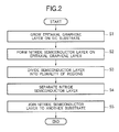
- FIG. 2 is a flow chart showing a manufacturing method of the nitride semiconductor substrate according to the first embodiment.
- the graphene layers 111a, 111b and 111c are grown on the SIC substrate 101 (step S1). Then, a nitride semiconductor layer 114 is grown on a surface of the graphene layers 111a, 111b and 111c (step S2). Then, the nitride semiconductor layer 114 is divided into a plurality of regions (step S3). Then, the nitride semiconductor layer 114 having been divided into regions is separated from the SiC substrate 101 (step S4). Then, the nitride semiconductor layer 114 is joined to another substrate, i.e., a second substrate which is different from the SiC substrate 101 (step S5).
- a second substrate which is different from the SiC substrate 101
- the nitride semiconductor layer 114 (particularly, GaN) has a hexagonal crystal structure whose symmetry is close to that of the epitaxial graphene layer 110, and therefore the nitride semiconductor layer 114 is joined to the graphene layer 110 only by physical bonding. For this reason, after the nitride semiconductor layer 114 is separated from the epitaxial graphene layer 110, crystal defects are not generated on a separation surface of the nitride semiconductor layer 114. That is, the separation surface the nitride semiconductor layer 114 has a flatness on the order of nanometer. Therefore, the nitride semiconductor layer 114 (having been separated from the graphene layer 110) can be joined to the second substrate 130 (described later) by intermolecular force.
- the epitaxial graphene layer 110 (i.e., the graphene layers 111a, 111b and 111c) is grown on the SiC substrate 101, so that the graphene-layer-grown substrate 200 ( FIG. 1A ) is obtained.
- the epitaxial graphene layer 110 is formed by performing high-temperature hydrogen etching process and high-temperature heating process on a surface of the SiC substrate 101 (see, Japanese Laid-Open Patent Publication No. 2009-62247 ).
- step S2 the process (step S2) for growing the nitride semiconductor layer 114 on the surface of the graphene-layer-grown substrate 200 ( FIG. 1A ) will be described with respect to FIG. 3 .
- a description herein will be made under the assumption that the nitride semiconductor is GaN.
- the graphene-layer-grown substrate 200 is placed in a crystal growth apparatus such as an MBE (Molecular Beam Epitaxy) apparatus or MOCVD (Metal Organic Chemical Vapor Deposition)apparatus. Then, the graphene-layer-grown substrate 200 is heated in the crystal growth apparatus, and gallium (Ga) and activated nitrogen are supplied to the crystal growth apparatus.
- the activated nitrogen is supplied by an electron cyclotron resonance (ECR) or a high-frequency excited radical source.
- ECR electron cyclotron resonance
- gallium (Ga) is adsorbed to a center portion of the honeycomb structure of carbon atoms of the graphene layer, so that a first layer having six-fold symmetry is formed. Further, activated nitrogen (N) is bonded to the first layer of gallium (Ga), so that a first layer of hexagonal GaN (h-GaN) is formed.
- Gallium (Ga) is not covalently bonded to the epitaxial graphene layer 110 (the graphene layers 111a, 111b and 111c), and therefore crystal defects due to lattice mismatch does not occur. For this reason, the nitride semiconductor layer 114 can be separated from the graphene layers 111a, 111b and 111c without causing crystal defects.
- the separated nitride semiconductor layer 114 has a separation surface with a flatness on the order of nanometers, and therefore the nitride semiconductor layer 114 can be joined to another substrate (i.e., the second substrate 130 described later) using intermolecular force.
- a single crystal GaN layer with a predetermined number of layers is formed. Since the first layer of GaN has no crystal defects (due to lattice mismatch), the resultant nitride semiconductor (GaN) layer has substantially no crystal defects. Thus, a high quality single crystal semiconductor layer is obtained.
- the nitride semiconductor layer 114 having a predetermined structure is formed on the surface of the epitaxial graphene layer 110 as shown in FIG. 3 . As a result, a nitride-semiconductor-layer/graphene-layer grown substrate 150 is formed as shown in FIG. 3 .
- FIGS. 4A and 4B show examples of the nitride semiconductor layer 114 that constitute light emitting elements.
- a nitride semiconductor layer 114A shown in FIG. 4A includes an n-type GaN layer 502, an n-type Al s Ga 1-s N (1 ⁇ s ⁇ 0) layer 503, a multiquantum well layer 504, a p-type Al t Ga 1-t N (1 ⁇ t ⁇ 0) layer 505 and a p-type GaN layer 506 which are layered in this order.
- the n-type GaN layer 502 and the n-type Al s Ga 1-s N layer 503 are doped with Si.
- the p-type Al t Ga 1-t N layer 505 and the p-type GaN layer 506 are doped with Mg.
- the multiquantum well layer 504 is composed of, for example, Ga y In 1-y N/Ga x In 1-x N/.../Ga x In 1-x N/Ga y In 1-y N/Ga x In 1-x N (1 ⁇ y ⁇ x ⁇ 0).
- a nitride semiconductor layer 114B shown in FIG. 4B includes a buffer layer 501 between the epitaxial graphene layer 110 ( FIG. 3 ) and the n-type GaN layer 502 of the nitride semiconductor layer 114A ( FIG. 4A ).
- the buffer layer 501 contains at least Ga.
- the buffer layer 501 is composed of, for example, Ga i In 1-i N (1 ⁇ i ⁇ 0) or Al j Ga 1-j N (1 ⁇ j ⁇ 0).
- a nitride semiconductor layer 114C shown in FIG. 4C includes a buffer layer 601 (for example, Ga i In 1-i N (1 ⁇ i ⁇ 0) or Al j Ga 1-j N (1 ⁇ j ⁇ 0)), an n-type GaN layer 602, an n-type Ga x In 1-x N (1 ⁇ x ⁇ 0) layer 603, a p-type Al y Ga 1-y N (1 ⁇ y ⁇ 0) layer 604 and a p-type GaN layer 605 which are layered in this order.
- the n-type GaN layer 602 is doped with Si.
- the p-type Al y Ga 1-y N layer 604 and the p-type GaN layer 605 are doped with Mg.
- the buffer layer 601 can be omitted as necessary.
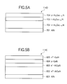
- FIG. 5A, 5B , 6A and 6B show examples of the nitride semiconductor layer that constitute other elements than light emitting elements.
- a nitride semiconductor layer 114D shown in FIG. 5A is used as, for example, a photodiode.
- the nitride semiconductor layer 114D includes a buffer layer 701 (for example, Ga i In 1-i N (1 ⁇ i ⁇ 0) or Al j Ga 1-j N (1 ⁇ j ⁇ 0)), an n-type Al x Ga 1-x N (1 ⁇ x ⁇ 0) layer 702, an i-type (intrinsic) Al y Ga 1-y N (1 ⁇ y ⁇ 0) layer 703 and a p-type Al x Ga 1-x N (1 ⁇ x ⁇ 0) layer 704 which are layered in this order.
- the buffer layer 701 can be omitted as necessary.
- a nitride semiconductor layer 114E shown in FIG. 5B is used as, for example, an HB-type (Hetero-Bipolar type) phototransistor.
- the nitride semiconductor layer 114E includes a buffer layer 801 (for example, Ga i In 1-i N (1 ⁇ i ⁇ 0) or Al j Ga 1-j N (1 ⁇ j ⁇ 0)), an n + -type Al x Ga 1-x N (1 ⁇ x ⁇ 0) layer 802, an n - -type Al y Ga 1-y N (1 ⁇ y ⁇ 0) layer 803, a p-type GaN layer 804 and p + -GaN layer 805 which are layered in this order.
- the buffer layer 801 can be omitted as necessary.
- a nitride semiconductor layer 114F shown in FIG. 6A is used as, for example, HEMT (High Electron Mobility Transistor).
- the nitride semiconductor layer 114F includes an undoped GaN layer 902, an undoped Al x Ga 1-x N (1 ⁇ x ⁇ 0) layer 903 and an n-type GaN layer 904 which are layered in this order.
- a nitride semiconductor layer 114G shown in FIG. 6B is used as, for example, MESFET (Metal Semiconductor Field Effect Transistor).
- the nitride semiconductor layer 114G includes an undoped GaN layer 1002 and an n-type GaN layer 1003 which are layered in this order.
- a buffer layer for example, Ga i In 1-i N (1 ⁇ i ⁇ 0) or Al j Ga 1-j N (1 ⁇ j ⁇ 0) below the undoped GaN layer 902 or the undoped GaN layer 1002.
- the step S3 ( FIG. 2 ) for dividing the nitride semiconductor layer 114 into a plurality of regions (with predetermined shapes) can be omitted in this embodiment.
- a supporting body adhesion layer 122 is formed on the stack of the nitride semiconductor layer 114 and the epitaxial graphene layer 110 on the SiC substrate 101.
- the supporting body adhesion layer 122 exhibits high adherence with the nitride semiconductor layer 114.
- An adhesive force (i.e., adhesive strength) between the surface of the supporting body adhesion layer 122 and the surface of the nitride semiconductor layer 114 is preferably greater than intermolecular force between the nitride semiconductor layer 114 and the graphene layer 111.
- the supporting body adhesion layer 122 is preferably composed of material with adhesiveness such as organic coating material that can be removed (exfoliated) using a removing liquid, or adhesive agent that exhibits removability when applied with heat, ultraviolet rays or the like.
- a supporting body 124 is adhered to the surface of the supporting body adhesion layer 122, for supporting the nitride semiconductor layer 114 (or the stack of the nitride semiconductor layer 114 and the epitaxial graphene layer 110) during the separation process thereof.
- the supporting body 124 has a function to support the nitride semiconductor layer 114 (or the stack of the nitride semiconductor layer 114 and the epitaxial graphene layer 110) after separation.
- the supporting body 124 preferably has an adhesion surface adhering to the supporting body adhesion layer 122 with an adhesive strength greater than intermolecular force between the respective graphene layers 111a, 111b and 111c.
- the supporting body 124 is preferably composed of a glass substrate, a ceramic substrate, a quartz substrate, a semiconductor substrate such as Si or the like.
- FIGS. 8A and 8B show a process in which the supporting body 124 is pulled upward so as to separate the nitride semiconductor layer 114 from the SiC substrate 101 (step S4 in FIG. 2 ).
- the supporting body 124 is pulled away from the SiC substrate 101 with a force F greater than the intermolecular force between the graphene layers 111a, 111b and 111c as shown in FIG. 8A , so that the graphene layer 111a and the graphene layer 111b are separated from each other.
- the nitride semiconductor layer 114 is separated from the graphene layer 111a as shown in FIG. 8B .
- FIG. 8A shows a state where the nitride semiconductor layer 114 and the graphene layer 111a are separated from the SiC substrate 101.
- the nitride semiconductor layer 114 and the graphene layers 111a and 111b are separated from the SiC substrate 101.
- FIGS. 9A and 9B are schematic views for illustrating intermolecular force between the nitride semiconductor layer 114 and the graphene layer 111a.
- FIG. 9A shows an interface between the nitride semiconductor layer 114 and the graphene layer 111a.
- FIG. 9B shows a state where, for example, the SiC substrate 101 and the graphene layer 111c are directly joined to each other.
- the nitride semiconductor layer 114 (particularly, GaN) has a crystal structure of hexagonal column. On each end surface of the hexagonal column, nitrogen (N) atoms are bonded to each other two-dimensionally in a hexagonal shape. In the graphene layer 111a, carbon (C) atoms are bonded to each other two-dimensionally in a hexagonal shape (see, FIG. 1B ). Therefore, as shown in FIG. 9A , nitrogen atoms (arranged in a hexagon) are disposed in between carbon atoms.
- the nitride semiconductor layer 114 and the graphene layer 111a are not covalently bonded to each other, but are physically bonded to each other due to regularity of potential at the surfaces (i.e., regularity of potential at atomic level at an interface therebetween).
- FIG. 9B shows a state where, for example, the SiC substrate 101 and the graphene layer 111c are directly joined to each other.
- the SiC substrate 101 has a crystal structure of tetrahedron. If the layers of SiC are stacked so that two layers form a stacking period, the SiC substrate 101 has a hexagonal symmetry. Therefore, the SiC substrate 101 is similar to the graphene layer 111c in having the hexagonal symmetry. However, the SiC substrate 101 does not have a hexagonal symmetry at a joint surface (i.e., a single layer). Therefore, the SiC substrate 101 and the graphene layer 111c are covalently bonded to each other. In other words, the SiC substrate 101 and the graphene layer 111c are not only bonded to each other by a weak force due to the regularity of potential, but also bonded to each other by a strong force via bonds.
- the bonding between the nitride semiconductor layer 114 and the graphene layer 111a, and the bonding between the graphene layers 111a and 111b are relatively weak.
- the bonding between the SiC substrate 101 and the graphene layer 111c is strong.
- a metamorphic layer is formed between the nitride semiconductor layer 114 and the graphene layer 111a, and therefore the bonding between the nitride semiconductor layer 114 and the graphene layer 111a is stronger than the bonding between the graphene layers 111a and 111b.
- the graphene layers 111a and 111b can be separated from each other, or the nitride semiconductor layer 103 can be separated from the graphene layer 111a, without forming crystal defects on the separation surface. Therefore, the separation surface has a flatness on the order of nanometers.
- the nitride semiconductor layer 114 is brought into direct contact with the surface of another substrate (i.e., the second substrate 130) as shown in FIG. 11A , and is fixed to the surface of the second substrate 130.
- the nitride semiconductor layer 114 and the graphene layer 111a are separated from the SiC substrate 101 (see FIG. 8A )
- the nitride semiconductor layer 114 and the graphene layer 111a are brought into direct contact with the surface of another substrate (i.e., the second substrate 130) as shown in FIG. 11B , and is fixed to the surface of the second substrate 130.
- step S5 the surface of the second substrate 130 and surface of the nitride semiconductor layer 114 (or the surface of the graphene layer 111a) are joined to each other by intermolecular force (see, step S5 ( FIG. 2 )).
- the nitride semiconductor layer 114 (or the nitride semiconductor layer 114 and the graphene layer 111a) can be brought into direct contact with a surface of a joining layer 132 formed on the second substrate 130 as shown in FIG. 12 , so as to be directly joined to the surface of the joining layer 132 by intermolecular force.
- the surface of the nitride semiconductor layer 114 (or the nitride semiconductor layer 114 and the graphene layer 111a) has a flatness on the order of nanometers.
- the flatness on the order of nanometers means that the surface roughness (to be more specific, a maximum valley depth Rrv, i.e., a maximum peak-to-valley difference) measured using an atomic force microscope (AFM) is smaller than 10 nm. It is more preferred that the surface roughness Rrv of the surface of the joining layer 132 formed on the second substrate 130 is smaller than or equal to 3 nm.
- the second substrate 130 is preferably, for example, a Si substrate, a ceramic substrate such as AlN substrate, a glass substrate, a quartz substrate, a plastic substrate or a metal substrate.
- the joining layer 132 formed on the second substrate 130 is preferably composed of material selected among, for example, SiO 2 , SiN, SiON, PSG, BSG, SOG, metal or organic substance.
- the joining layer 132 is formed using, for example, plasma CVD method, CVD method or sputtering method.
- the nitride semiconductor layer 114 (or the graphene layer 111a) is joined to the second substrate 130 (or the joining layer 132) by means of atomic diffusion or compound formation via the interface, instead of intermolecular force.
- the supporting body adhesion layer 122 and the supporting body 124 are removed from the surface of the nitride semiconductor layer 114, as shown in FIGS. 13A and 13B .
- the removing of the,supporting body adhesion layer 122 and the supporting body 124 can be performed by removing the supporting body adhesion layer 122 using removing liquid, heat or ultraviolet rays.
- the supporting body adhesion layer 122 and the supporting body 124 are removed using removing liquid (etching liquid)
- removing liquid etching liquid
- FIG. 13A shows a nitride semiconductor substrate 160A in which the nitride semiconductor layer 114 is joined to the surface of the second substrate 130.
- FIG. 13B shows a nitride semiconductor substrate 160B in which the stack of the nitride semiconductor layer 114 and the graphene layer 111a is joined to the surface of the second substrate 130.
- FIG. 14A shows a nitride semiconductor substrate 160C in which the stack of the nitride semiconductor layer 114 and the graphene layer 111a is joined to the surface of the second substrate 130 via the joining layer 132.
- FIG. 14B shows a nitride semiconductor substrate 160D in which the nitride semiconductor layer 114 is joined to the surface of the second substrate 130 via the joining layer 132.
- the nitride semiconductor layer 114 is joined to the second substrate 130 by intermolecular force.
- the stack of the nitride semiconductor layer 114 and the graphene layer 111a is joined to the second substrate 130 by intermolecular force.
- the stack of the nitride semiconductor layer 114 and the graphene layer 111a is joined to the second substrate 130 via the joining layer 132 by intermolecular force.
- the nitride semiconductor layer 114 is joined to the second substrate 130 via the joining layer 132 by intermolecular force.
- the nitride semiconductor substrates 160B and 160C FIGS. 13B and 14A ) in which the stack of the nitride semiconductor layer 114 and the graphene layer 111a is joined to the second substrate 130, functional devices such as graphene transistors can be manufactured.
- the nitride semiconductor layer 114 is grown on the epitaxial graphene layer 110 having been grown on the SiC substrate 101 (the first substrate), and the nitride semiconductor layer 114 is separated from the SiC substrate 101 using a force greater than the intermolecular force between the graphene layers 111a, 111b and 111c or greater the intermolecular force between the graphene layer 111a and the nitride semiconductor layer 114. Therefore, the nitride semiconductor layer 114 can be easily separated from the SiC substrate 101.
- the separation surface of the nitride semiconductor layer 114 or the graphene layer 111a has a flatness on the order of nanometers (i.e., i.e., a surface roughness smaller than 10 nm), and therefore the nitride semiconductor layer 114 (or the nitride semiconductor layer 114 and the graphene layer 111a) can easily be joined to the second substrate 130 via intermolecular force or the like.
- the supporting body adhesion layer 122 is integrally formed with the supporting body 124.
- the epitaxial graphene layer 110 is grown on the SiC substrate 101 (i.e., the first substrate), and the nitride semiconductor layer 114 is grown on the epitaxial graphene layer 110.
- the nitride semiconductor layer 114 is configured as, for example, the nitride semiconductor layer 114A, 114B, 114C, 114D, 114E, 114F or 114G shown in FIGS. 4A through 6F .
- the nitride semiconductor layer 114 is fabricated into predetermined element shapes so that a plurality of elements are formed on the nitride semiconductor layer 114.
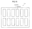
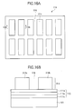
- the nitride semiconductor layer 114 is divided into a plurality of element formation regions 214 and a non-element formation region 216.
- the element formation regions 214 are respectively formed as isolated islands 314.
- the non-element formation region 216 is formed so as to include isolating grooves that isolate respective isolated islands 314.
- respective isolated islands 314 have elongated rectangular shapes, and arranged in two rows and six columns.
- FIG. 16A is a plan view showing the nitride semiconductor layer 114.
- FIG. 16B is a sectional view of the graphene-layer-grown substrate with the nitride semiconductor layer 114 taken along line 16B-16B in FIG. 16A .
- the isolating grooves 316 are illustrated so as to reach an upper surface of the epitaxial graphene layer 110.
- the isolating grooves 316 can be formed so as to reach the surface (or inside) of the SiC substrate 101.
- the isolating grooves 316 are not limited to vertically extending grooves.
- the supporting body adhesion layer 122 and the supporting body 124 are formed thereon as described in the first embodiment. Thereafter, the isolated islands 314 (the nitride semiconductor layer 114) are separated from the SiC substrate 101 with a force greater than the intermolecular force between the graphene layers 111a and 111b (see, FIG. 8A ). Alternatively, the isolated islands 314 (the nitride semiconductor layer 114) are separated from the SiC substrate 101 with a force greater than the intermolecular force between the graphene layer 111a and the nitride semiconductor layer 114 (see, FIG. 8B ). With such a process, the isolated islands 314 are separated from the SiC substrate 101.
- the isolated islands 314 are separated from the SiC substrate 101
- the isolated islands 314 are joined to predetermined positions on the surface of another substrate (i.e., the second substrate 130) as described in the first embodiment, so as to form a nitride semiconductor substrate 160E.
- the isolated islands 314 are joined to predetermined positions on the surface of the joining layer 132 on the second substrate 130 as described in the first embodiment, so as to form a nitride semiconductor substrate 160E.
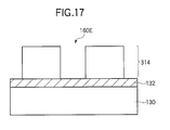
- FIG. 17 shows a nitride semiconductor substrate 160E in which the isolated islands 314 are joined to the surface of the joining layer 132 formed on the second substrate 130.
- the separation surfaces of the isolated islands 314 have surface roughness (to be more specific, the maximum valley roughness Rrv, i.e, the maximum peak-to-valley difference) smaller than 10 nm when measured using the atomic force microscope (AFM). Since the isolated islands 314 have such flat separation surfaces, excellent joint can be obtained between the separation surfaces of the isolated islands 314 and the second substrate 130 (or the joining layer 132).
- the nitride semiconductor layer 114 (divided into the isolated islands 314 by the isolation grooves 316) is described to form elements such as light emitting elements or electron elements, it means that the isolated islands 314 are completed as the elements which are operable.
- the nitride semiconductor layer 114 is described to be in the process of forming the elements (such as light emitting elements or electron elements), it means that the isolated islands 314 have not yet been completed as the elements, and it also means that the nitride semiconductor layer 114 has not yet fabricated into predetermined elements.
- the nitride semiconductor layer 114 is fabricated into the isolated islands 314 having predetermined shapes by forming the grooves 316, in addition to the process according to the first embodiment. Accordingly, the nitride semiconductor layer 114 (that forms the elements or that is in the process of forming the elements) can be easily separated from the SiC substrate 101.
- the third embodiment of the present invention is different from the first and second embodiment in the following aspects.
- the nitride semiconductor layer 114 is grown on the epitaxial graphene layer 110 having been grown on the SiC substrate 101 (i.e., the first substrate), so as to form a nitride-semiconductor-layer/graphene-layer grown substrate 400.
- a surface of the nitride-semiconductor-layer/graphene-layer grown substrate 400 i.e., a surface of the nitride semiconductor layer 114 opposite to the graphene layer 111a side
- the SiC substrate 101 is separated from the nitride semiconductor layer 104.
- the third embodiment will be described with reference to FIGS. 18A, 18B , 19A and 19B .
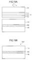
- FIG. 18A shows a process in which the nitride-semiconductor-layer/graphene-layer grown substrate 400 (in which the epitaxial graphene layer 110 and the nitride semiconductor layer 114 are formed on the SiC substrate 101) is jointed to the second substrate 130 with the joining layer 432.
- the joining layer 432 has a function to joint the second substrate 130 and the nitride semiconductor layer 114 to each other with a force which is greater than a force required for separating the SiC substrate 101 as described later ( FIG. 19A ).
- FIG. 18B shows a process in which the surface of the nitride semiconductor layer 114 is jointed to the joining layer 432.
- the second substrate 130, the joining layer 432, the epitaxial graphene layer 110 and the SiC substrate 101 are layered from the bottom to the top in this order.
- the SiC substrate 101 is pulled away from the second substrate 130 with the force F greater than the intermolecular force between the graphene layers 111a and 111b or greater the intermolecular force between the graphene layer 111a and the nitride semiconductor layer 114, so as to separate the SiC substrate 101 from the second substrate 130.
- the force F is smaller than the joint force between the SiC substrate 101 and the graphene layer 111c.
- FIG. 19B shows a state after the SiC substrate 101 is separated from the second substrate 130, so that a nitride semiconductor substrate 160F is formed.
- the nitride semiconductor substrate 160F includes the second substrate 130, the joining layer 432 and the nitride semiconductor layer 114 which are layered from the bottom to the top in this order.
- the nitride semiconductor layer 114 can be divided into a plurality of regions as described in the second embodiment.
- the nitride semiconductor layer 114 can be configured as light emitting elements or electron elements.
- the nitride semiconductor layer 114 is formed on the surface of the epitaxial graphene layer 110 having been grown on the SiC substrate 101 so as to form the nitride-semiconductor-layer/graphene-layer grown substrate 400, and the surface of the nitride semiconductor layer 114 opposite to the graphene layer 111a is joined to the second substrate 130 (or the joint surface 432 formed on the second substrate 130). Thereafter, the SiC substrate 101 is separated from the nitride semiconductor layer 114. Accordingly, in addition to the advantageous of the first and second embodiments, a process for forming the supporting body (for supporting the nitride semiconductor layer during the separation process) can be omitted.
- FIGS. 20A through 20E are schematic views for illustrating the manufacturing method of the graphene substrate 100 according to the fourth embodiment.
- FIG. 21 shows the single crystal nitride semiconductor wafer 300 in which the nitrides semiconductor layer 114 is formed on the surface of the graphene substrate 100.
- FIG. 22 is a flow chart showing a manufacturing process of the single crystal nitride semiconductor wafer 300 using the graphene substrate 100.
- the epitaxial graphene layer 110 (including the graphene layers 111a, 111b and 111c) is formed on the surface of the SiC substrate 101, so as to form a graphene-layer-grown substrate 200 (step S11).
- a metal adhesion layer 120 is formed on the surface of the epitaxial graphene layer 110 on the SiC substrate 101 (step S12).
- the metal adhesion layer 120 is composed of material that tends to diffuse into the inside of the epitaxial graphene layer 110 from the surface of the epitaxial graphene layer 110.
- the metal adhesion layer 120 is used for separating the graphene layer 111a from the other graphene layers 111b and 111c as described later.
- the metal adhesion layer 120 is composed of, for example, a titan (Ti) layer, and is formed on the entire surface of a wafer (i.e., on the epitaxial graphene layer 110 on the SiC substrate 101) by vacuum deposition. Titan (Ti) of the metal adhesion layer (i.e., the Ti layer) 120 is diffused into the graphene layer 111a, with the result that the metal adhesion layer 120 and the graphene layer 111a are strongly joined to each other due to adhering effect such as anchoring effect. In other words, the metal adhesion layer 120 and the graphene layer 111a are joined to each other with a stronger force than the intermolecular force between the graphene layers 111a, 111b and 111c.
- Ti titan
- the supporting body adhesion layer 122 is formed on the surface of the metal adhesion layer 120 (step S13).
- the supporting body adhesion layer 122 exhibits high adhesion with the metal adhesion layer 120.
- the supporting body 124 is adhered to the surface of the supporting body adhesion layer 122.
- the supporting body 124 is provided for supporting the graphene layer 111a when the graphene layer 111a is separated from the other graphene layers 111b and 111c as described later.
- the supporting body 124 is pulled away from the SiC substrate 101 with a force F greater than the intermolecular force between the graphene layers 111a, 111b and 111c, so as to separate the graphene layer 111a from the graphene layer 111b (step S14).
- the metal adhesion layer 120 and the graphene layer 111a are separated from the SiC substrate 101 in FIG. 20C , it is also possible that the metal adhesion layer 120 and a plurality of graphene layers (for example, the graphene layers 111a and 111b) are separated from the SiC substrate 101.
- the SiC substrate 101 has a crystal structure of tetrahedron. If the layers of SiC are stacked so that two layers form a stacking period, the SiC substrate 101 has a hexagonal symmetry. Therefore, the SiC substrate 101 is similar to the graphene layer 111c in having the hexagonal symmetry. However, the SiC substrate 101 does not have a hexagonal symmetry at a joint surface (i.e., a single layer). Therefore, the SiC substrate 101 and the graphene layer 111c are covalently bonded to each other.
- the SiC substrate 101 and the graphene layer 111c are not only bonded to each other by a weak force due to regularity of potential, but also bonded to each other by a strong force via bonds.
- the bonding between the respective graphene layers 111a, 111b and 111c is relatively weak.
- the bonding between the SiC substrate 101 and the graphene layer 111c is strong.
- the joining layer 132 is formed on the surface of another substrate, i.e., the second substrate 130 (step S14). Thereafter, the graphene layer 111a is brought into direct contact with the surface of the joining layer 132, so that the graphene layer 111a is fixed to the surface of the joining layer 132 (step S15). The surface of the joining layer 132 and the surface of the graphene layer 111a are joined to each other by the intermolecular force.
- the joining layer 132 provides excellent joint with the second substrate 130 and the graphene layer 111a. In this regard, "excellent joint" means that a joint strength is uniform throughout joint surfaces, void does not generated at the joint interfaces, and no crack occurs at the joint surfaces.
- the second substrate 130 is, for example, a Si substrate.
- the joining layer 132 is, for example, a SiO 2 layer.
- the metal adhesion layer 120, the supporting body adhesion layer 122 and the supporting body 124 are removed from the surface of the graphene layer 111a (step S16).
- the metal adhesion layer 120 is removed by chemical etching using acid such as hydrofluoric acid, with the result that the metal adhesion layer 120, the supporting body adhesion layer 122 and the supporting body 124 are removed.
- the graphene substrate 100 in which the graphene layer 111a is formed on the second substrate 130 is obtained (step S17).
- the single crystal semiconductor layer 114 is grown on the surface of the graphene substrate 100, so as to form a single crystal nitride semiconductor wafer 300 (step S18).
- the joining layer 132 formed on the second surface 130 and the graphene layer 111a are jointed to each other by intermolecular force, and the graphene layer 111a and the nitrides semiconductor layer 114 are joined to each other by intermolecular force.
- the surface of the graphene layer 111a has a flatness on the order of nanometers.
- the flatness on the order of nanometers means that the surface roughness (to be more specific, the maximum valley depth Rrv, i.e., the maximum peak-to-valley difference) measured using the atomic force microscope (AFM) is smaller than 10 nm. It is more preferred that the surface roughness Rrv of the joining layer 132 formed on the second substrate 130 is smaller than or equal to 3 nm.
- the second substrate 130 is preferably, for example, a Si substrate, a ceramic substrate such as AlN substrate, a glass substrate, a quartz substrate, a plastic substrate or a metal substrate.
- the joining layer 132 formed on the second substrate 130 is preferably composed of material selected among, for example, SiO 2 , SiN, SiON, PSG, BSG, SOG, metal and organic substance.
- the joining layer 132 is formed using, for example, plasma CVD method, CVD method or sputtering method.
- the joining layer 132 and the graphene layer 111a are joined to each other by means of atomic diffusion or compound formation via the interface, instead of intermolecular force.
- the graphene substrate 100 is placed into the crystal growth apparatus such as an MBE apparatus or MOCVD apparatus.
- the graphene substrate 100 is heated in the crystal growth apparatus, and gallium (Ga) and activated nitrogen are supplied into the crystal growth apparatus.
- the activated nitrogen is supplied by an electron cyclotron resonance (ECR) or a high-frequency excited radical source.
- ECR electron cyclotron resonance
- the nitride semiconductor layer 114 (particularly, GaN) has a crystal structure of hexagonal column. On each end surface of the hexagonal column, nitrogen (N) atoms are bonded to each other two-dimensionally in a hexagonal shape. In the graphene layer 111a, carbon (C) atoms are bonded to each other two-dimensionally in a hexagonal shape (see FIG. 1B ). Nitrogen atoms (arranged in a hexagon) are disposed in between carbon atoms. Therefore, the nitride semiconductor layer 114 and the graphene layer 111a are not covalently bonded to each other, but are physically bonded to each other due to regularity of potential at the surfaces (i.e., regularity of potential at atomic level at the interface therebetween).
- Gallium (Ga) is not covalently bonded to the graphene layer 111a, and therefore crystal defects due to lattice mismatch does not occur.
- second and third GaN layers and succeeding GaN layers if needed
- a single crystal GaN layer with a predetermined number of layers is formed.
- the resultant GaN layer has remarkably few crystal defects, i.e., a high quality single crystal semiconductor layer is obtained.
- a semiconductor wafer in which a high quality single crystal nitride gallium (GaN) layer with substantially no crystal defects is' formed on a surface of a large diameter Si substrate.
- the single crystal nitride semiconductor layer 114 is grown on the surface of the graphene substrate 100 in which the graphene layer 111a is joined to the surface of the second substrate 130 by means of intermolecular force.
- a low-cost, large-diameter Si substrate can be used as the second substrate 130, and therefore a low-cost, large-diameter single crystal nitride semiconductor layer growth wafer can be obtained.
- the second substrate 130 can be selected among various options, and therefore optimum substrate best suited for application can be selected.
- the fourth embodiment can be applied to crystal growth of other nitride semiconductor layer 114, for example, Al x Ga 1-x N (1 ⁇ x ⁇ 0), In x Ga 1-x N (1 ⁇ x ⁇ 0) and Al x In 1-x N (1 ⁇ x ⁇ 0).
- the nitride semiconductor layer 114 is grown on the graphene layer 111a due to regularity of specific potential at the surfaces of the graphene layer 111a and the nitride semiconductor layer 114, without utilizing covalent bonding. Therefore, the fourth embodiment can be applied to crystal growth of other semiconductor layer (i.e., other than the nitride semiconductor layer) such as III-V group compound semiconductor layer, II-VI group compound semiconductor layer or IV-IV group compound semiconductor layer.
- other semiconductor layer i.e., other than the nitride semiconductor layer
- the fifth embodiment of the present invention is different from the fourth embodiment in that the single crystal nitride semiconductor layer is grown on the substrate on which the epitaxial graphene layer has been formed.
- the fifth embodiment will be described with reference to FIGS. 23A and 23B .
- FIG. 23A shows the graphene-layer-grown substrate 200.
- the epitaxial graphene layer 110 is formed on the surface of the SiC substrate 101 using the method having been described in the fourth embodiment, so as to form the graphene-layer-grown substrate 200.
- the epitaxial graphene layer 110 includes three graphene layers 111a, 111b and 111c.
- gallium nitride (GaN) is formed on the surface of the graphene-layer-grown substrate 200 using the MBE method or MOCVD method.
- gallium (Ga) and activated nitrogen are introduced into the crystal growth apparatus, gallium (Ga) is adsorbed onto a center portion of the honeycomb structure of carbon atoms of the graphene layer 111a, so that a first layer having six-fold symmetry is formed.
- activated nitrogen is adsorbed onto the first layer of gallium (Ga), so that a first layer of hexagonal GaN (h-GaN) is formed.
- the activated nitrogen is supplied by an electron cyclotron resonance (ECR) or a high-frequency excited radical source.
- Second and third GaN layers (and succeeding GaN layers if needed) on the first GaN layer, a single crystal GaN layer with a predetermined number of layers is formed.
- FIG. 23B shows a semiconductor wafer 400 in which the nitride semiconductor layer 114 is formed on the surface of the graphene-layer-grown substrate 200.
- the nitrides semiconductor layer 114 is composed of a semiconductor material selected among, for example, Al x Ga 1-x N (1 ⁇ x ⁇ 0), Al x In 1-x N (1 ⁇ x ⁇ 0) and In x Ga 1-x N (1 ⁇ x ⁇ 0), either alone or in combination. Further, the nitrides semiconductor layer 114 can be composed of a compound semiconductor material that contains nitrogen.
- the single crystal semiconductor wafer 400 can be manufactured without a transferring (i.e., separating and joining) process of the graphene layer 111a. Therefore, even if lattice mismatch exists, a high quality single crystal semiconductor layer (in which the epitaxial graphene layer 110 is joined to the SiC substrate 101 by intermolecular force) with substantially no crystal defects can be manufactured.
- the SiC substrate 101 has been used.
Landscapes
- Recrystallisation Techniques (AREA)
- Led Devices (AREA)
Abstract
Description
- The present invention relates to a separation method of nitride semiconductor layer, a semiconductor device and a manufacturing method thereof.
- The present invention also relates to a semiconductor wafer, and a manufacturing method thereof.
- As an example of a conventional manufacturing method of a semiconductor device, Patent Document No. 1 discloses a manufacturing method of an LED (Light Emitting Diode), in which a buffer layer, an n-type nitride semiconductor layer, an active layer, a p-type nitride semiconductor layer, an n-type contact layer are grown on a sapphire substrate in this order so as to form a semiconductor wafer. Further, these layers are etched so as to partially remove the n-type contract layer, the p-type nitride semiconductor layer and the active layer, and to expose the n-type nitride semiconductor layer. Then, an Al (aluminum) electrode is formed on the exposed surface of the n-type nitride semiconductor layer and on the surface of the n-type contact layer using a deposition method. Thereafter, a heat treatment is performed to ensure a sufficient contact.
- The growth of the above described layers (i.e., semiconductor epitaxial layers) is carried out using an MOCVD (Metal Organic Chemical Vapor Deposition) method. Using such a method, a nitride LED with high light emission efficiency is manufactured.
- Recently, there is a need for integration of LEDs formed of different materials or integration of semiconductor devices with different functions. For this reason, it is preferred to separate the epitaxial semiconductor layers from the sapphire substrate (referred to as a first substrate), and to fix the semiconductor epitaxial layers to another substrate (referred to a second substrate).
- Conventionally, there is proposed a laser lift-off method, in which a laser beam is irradiated onto a backside of the sapphire substrate to thereby decompose the nitride semiconductor layer in the vicinity of the sapphire substrate, by which the semiconductor epitaxial layers can be separated from the sapphire substrate. To be more specific, the laser beam irradiation onto the backside of the sapphire substrate causes GaN (gallium nitride) to be decomposed into Ga (gallium) and N (nitrogen) at an interface between the sapphire substrate and the nitride semiconductor layer. Since a melting point of Ga is at a room temperature, the semiconductor epitaxial layers can be separated from the sapphire substrate.
- In this method, however, a separation surface of the semiconductor epitaxial layers separated from the sapphire substrate does not have a sufficient flatness (i.e., on the order of nanometers).
- In order to join the nitride semiconductor epitaxial layers to a second substrate different from the first substrate (the sapphire substrate) using intermolecular force, it is preferred that the separation surface of the semiconductor epitaxial layers has a flatness on the order of nanometers. If the separation surface of the semiconductor epitaxial layers (separated from the first substrate) does not have a flatness on the order of nanometers, a sufficient intermolecular force (i.e., a joint force) is not obtained.
- Therefore, in the method disclosed in Patent Document No. 1, it is necessary to perform a surface treatment to enhance the flatness of the separation surface of the semiconductor epitaxial layers, after the above described separation process using the lift-off method.
- Meanwhile, a semiconductor crystal growth technology has been developed mainly for growing semiconductor layers on a lattice-matched substrate. Recently, a non-equilibrium epitaxial growth technology such as MBE (Molecular Beam Epitaxy) or MOCVD (Metal Organic Chemical Vapor Deposition) has been developed for growing semiconductor layers on a lattice mismatched substrate. In this regard, for example, Patent Document No. 2 discloses a manufacturing method of a nitride semiconductor device, in which a stack of an amorphous nitride layer and a GaN buffer layer is formed on a surface of a sapphire substrate, and then nitride semiconductor layers are grown on the stack.
- However, in the method disclosed in Patent Document No. 2, there is a lattice mismatch of approximately 10% between the nitride semiconductor layers and the sapphire substrate. When crystal growth is performed while maintaining a covalent bonding with the substrate, crystal defects may be formed due to such a lattice mismatch at an interface. Therefore, there is a limit in enhancement of crystal characteristics of the grown nitride semiconductor layers.
- In this regard, a high quality and large diameter nitride semiconductor wafer is still in the process of development. Therefore, there has been a demand for a crystal growth technology of high quality and large diameter single crystal nitride semiconductor on a lattice mismatched substrate.
- Patent Document No. 1: Japanese Laid-Open Patent Publication No.
2006-135311 - Patent Document No. 2: Japanese Laid-Open Patent Publication No.
H09-18053 - The present invention is intended to provide a separation method of a nitride semiconductor layer, a semiconductor device and a manufacturing method thereof capable of facilitating separation of the nitride semiconductor layer from a substrate.
- Further, the present invention is intended to provide a semiconductor wafer and a manufacturing method thereof capable of producing high quality single crystal nitride semiconductor substantially free from crystal defects by means of crystal growth on a lattice mismatched substrate.
- The present invention provides a separation method of a nitride semiconductor layer. The separation method includes the steps of: growing a graphene layer in the form of a single layer or two or more layers on a surface of a first substrate, forming a nitride semiconductor layer on the graphene layer so that the nitride semiconductor layer is bonded to the graphene layer with a bonding force due to regularity of potential at atomic level at an interface therebetween without utilizing covalent bonding, and separating the nitride semiconductor layer from the first substrate with a force which is greater than the bonding force between the nitride semiconductor layer and the graphene layer, or greater than a bonding force between layers of the graphene layer.
- The present invention also provides a manufacturing method of a nitride semiconductor device. The manufacturing method includes the above described separation method of the nitride semiconductor layer. The manufacturing method further includes the step of joining the nitride semiconductor layer to a surface of a second substrate.
- The present invention also relates to a manufacturing method of a semiconductor device, the manufacturing method comprising the steps of: growing a graphene layer in the form of a single layer or two or more layers on a surface of a first substrate, forming a nitride semiconductor layer on the graphene layer so that the nitride semiconductor layer is bonded to the graphene layer with a bonding force due to regularity of potential at atomic level at an interface therebetween without utilizing covalent bonding, joining a surface of the nitride semiconductor layer to a surface of a second substrate, and separating the nitride semiconductor layer from the first substrate with a force which is greater than the bonding force between the nitride semiconductor layer and the graphene layer.
- The present invention also provides a semiconductor device including a nitride semiconductor layer formed by growing the nitride semiconductor layer on a graphene layer in the form of a single layer or two or more layers on a first substrate so that the nitride semiconductor layer is bonded to the graphene layer with a bonding force due to regularity of potential at atomic level at an interface therebetween without utilizing covalent bonding, separating the nitride semiconductor layer from the first substrate with a force which is greater than the bonding force between the nitride semiconductor layer and the graphene layer, or greater than a bonding force between layers of the graphene layer, and joining the nitride semiconductor layer to a surface of the second substrate.
- The present invention also provides a manufacturing method of a semiconductor wafer in which a single crystal semiconductor layer is grown on a surface of a semiconductor substrate. The manufacturing method includes the steps of: providing a graphene layer on the surface of the semiconductor substrate, forming a first layer of the single crystal semiconductor layer on the graphene layer in such a manner that one constituent element of a crystal of the single crystal semiconductor layer is adsorbed to a center portion of a honeycomb structure of carbon atoms of the graphene layer, and the other constituent element of the crystal is bonded to the one constituent element, and growing the single crystal semiconductor layer on a surface of the first layer.
- The present invention also provides a semiconductor wafer in which a single crystal semiconductor layer is grown on a surface of a substrate. The semiconductor wafer includes the substrate, a graphene layer provided on a surface of the substrate, and the single crystal semiconductor layer grown on a surface of the graphene layer. The single crystal semiconductor layer is formed in such a manner that one constituent element of a crystal of the single crystal semiconductor layer is adsorbed to a center portion of a honeycomb structure of carbon atoms of the graphene layer, and the other constituent element of the crystal is bonded to the one constituent element.
- Further scope of applicability of the present invention will become apparent from the detailed description given hereinafter. However, it should be understood that the detailed description and specific embodiments, while indicating preferred embodiments of the invention, are given by way of illustration only, since various changes and modifications within the spirit and scope of the invention will become apparent to those skilled in the art from this detailed description.
- In the attached drawings:
-
FIG. 1A is a sectional view showing a graphene-layer-grown substrate according to a first embodiment of the present invention; -
FIG. 1B is a schematic perspective view showing a structure of the epitaxial graphene layer; -
FIG. 2 is a flow chart showing a manufacturing method of a nitride semiconductor substrate according to the first embodiment of the present invention; -
FIG. 3 is a sectional view showing the graphene-layer-grown substrate with a nitride semiconductor layer according to the first embodiment of the present invention; -
FIGS. 4A, 4B and 4C are sectional views respectively showing examples of the nitride semiconductor layer according to the first embodiment of the present invention; -
FIGS. 5A and 5B are sectional views respectively showing examples of the nitride semiconductor layer according to the first embodiment of the present invention; -
FIGS. 6A and 6B are sectional views respectively showing examples of the nitride semiconductor layer according to the first embodiment of the present invention; -
FIG. 7A is a sectional view showing the graphene-layer grown substrate with the nitride semiconductor layer on which a supporting body adhesion layer is provided, according to the first embodiment of the present invention; -
FIG. 7B is a sectional view showing the graphene-layer-grown substrate with the nitride semiconductor layer on which the supporting body adhesion layer and a supporting body are provided, according to the first embodiment of the present invention; -
FIG. 8A is a sectional view showing a process where the supporting body is pulled so as to cause a separation between graphene layers at a bonding surface, according to the first embodiment of the present invention; -
FIG. 8B is a sectional view showing a process in which the supporting body is pulled so as to cause a separation of the nitride semiconductor layer from the epitaxial graphene layer at a bonding surface therebetween, according to the first embodiment of the present invention; -
FIGS. 9A and 9B are schematic views showing states at the bonding surface between the nitride semiconductor layer and the epitaxial graphene layer, according to the first embodiment of the present invention; -
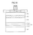
FIG. 10 is a sectional view for illustrating a process separating the nitride semiconductor layer from a SiC substrate by means of vacuum suction, according to the first embodiment of the present invention; -
FIGS. 11A and 11B are sectional views respectively showing a process in which the nitride semiconductor layer is joined to a second substrate, according to the first embodiment of the present invention; -
FIG. 12 is a sectional view showing a structure of the second substrate with a joining layer formed thereon, according to the first embodiment of the present invention; -
FIGS. 13A and 13B are sectional views respectively showing structures of the second substrate with the nitride semiconductor layer joined thereto, according to the first embodiment of the present invention; -
FIGS. 14A and 14B are sectional views respectively showing structures of the second substrate with the nitride semiconductor layer joined thereto via joining layers, according to the first embodiment of the present invention; -
FIG. 15 is a plan view showing a nitride semiconductor layer divided into isolated islands, according to the second embodiment of the present invention; -
FIG. 16A is a plan view showing the nitride semiconductor layer divided into isolated islands, according to the second embodiment of the present invention; -
FIG. 16B is a sectional view showing the graphene-layer-grown substrate with the nitride semiconductor layer divided into isolated islands taken alongline 16B-16B inFIG. 16A ; -
FIG. 17 is a sectional view showing the nitride semiconductor substrate with isolated islands, according to the second embodiment; -
FIGS. 18A and 18B are sectional views respectively showing a process in which a stack of a SiC substrate, an epitaxial graphene layer and a nitride semiconductor layer is joined to a second substrate, according to the third embodiment of the present invention; -
FIGS. 19A and 19B are sectional views respectively showing a process in which SiC substrate is separated from the nitride semiconductor layer, according to the third embodiment of the present invention; -
FIGS. 20A through 20E are sectional views for illustrating a manufacturing process of a semiconductor substrate according to the fourth embodiment of the present invention; -
FIG. 21 is a sectional view showing a single crystal nitride semiconductor wafer according to the third embodiment of the present invention; -
FIG. 22 is a flow chart showing a manufacturing process of the single crystal nitride semiconductor wafer according to the third embodiment of the present invention; -
FIG. 23A is a sectional view showing a graphene-layer grown substrate according to the fifth embodiment of the present invention; and -
FIG. 23B is a sectional view showing a single crystal semiconductor wafer according to the fifth embodiment of the present invention. - Hereinafter, embodiments of the present invention will be described with reference to drawings. The present invention is not limited to the embodiment described below, and modifications and improvements may be made to the invention without departing from the spirit and scope of the invention.
-
FIGS. 1A through 13B are views for illustrating a separation method of a semiconductor layer (i.e., a semiconductor thin film) and a manufacturing method of a nitride semiconductor device according to the first embodiment of the present invention. -
FIG. 1A shows a graphene-layer-grown substrate 200 (i.e., a substrate with an epitaxial graphene layer) according to the first embodiment of the present invention. The graphene-layer-grownsubstrate 200 includes aSiC substrate 101 as a first substrate (i.e., a semiconductor substrate) and anepitaxial graphene layer 110 formed on thesubstrate 101. Theepitaxial graphene layer 110 is in the form of a single layer, or two or more layers. In this example, theepitaxial graphene layer 110 includes threegraphene layers -
FIG. 1B schematically shows a structure of theepitaxial graphene layer 110. Theepitaxial graphene layer 110 includes threegraphene layers graphene layers FIG. 1B , the carbon atoms of thegraphene sheet 111a are shown by black circles, the carbon atoms of thegraphene sheet 111b are shown by dotted circles, and carbon atoms of thegraphene sheet 111c are shown by white circles. - A graphene is a new material with a unique band-structure and described as massless fermions. A graphene substantially has electrical properties (for example, ballistic transport) similar to that of carbon nanotubes (CNT) having a cylindrical shape. Unlike CNTs, a graphene has a sheet-like structure, and therefore compatible with microfabrication process (for conventional LSI), which is advantageous in facilitating integration.
- Next, a method of separating a nitride semiconductor layer from the SiC substrate, and joining the nitride semiconductor layer to another substrate will be described with reference to
FIG. 2. FIG. 2 is a flow chart showing a manufacturing method of the nitride semiconductor substrate according to the first embodiment. - First, the
graphene layers nitride semiconductor layer 114 is grown on a surface of thegraphene layers nitride semiconductor layer 114 is divided into a plurality of regions (step S3). Then, thenitride semiconductor layer 114 having been divided into regions is separated from the SiC substrate 101 (step S4). Then, thenitride semiconductor layer 114 is joined to another substrate, i.e., a second substrate which is different from the SiC substrate 101 (step S5). The nitride semiconductor layer 114 (particularly, GaN) has a hexagonal crystal structure whose symmetry is close to that of theepitaxial graphene layer 110, and therefore thenitride semiconductor layer 114 is joined to thegraphene layer 110 only by physical bonding. For this reason, after thenitride semiconductor layer 114 is separated from theepitaxial graphene layer 110, crystal defects are not generated on a separation surface of thenitride semiconductor layer 114. That is, the separation surface thenitride semiconductor layer 114 has a flatness on the order of nanometer. Therefore, the nitride semiconductor layer 114 (having been separated from the graphene layer 110) can be joined to the second substrate 130 (described later) by intermolecular force. - In the step S1, the epitaxial graphene layer 110 (i.e., the
graphene layers SiC substrate 101, so that the graphene-layer-grown substrate 200 (FIG. 1A ) is obtained. Theepitaxial graphene layer 110 is formed by performing high-temperature hydrogen etching process and high-temperature heating process on a surface of the SiC substrate 101 (see, Japanese Laid-Open Patent Publication No.2009-62247 - Here, the process (step S2) for growing the
nitride semiconductor layer 114 on the surface of the graphene-layer-grown substrate 200 (FIG. 1A ) will be described with respect toFIG. 3 . A description herein will be made under the assumption that the nitride semiconductor is GaN. The graphene-layer-grownsubstrate 200 is placed in a crystal growth apparatus such as an MBE (Molecular Beam Epitaxy) apparatus or MOCVD (Metal Organic Chemical Vapor Deposition)apparatus. Then, the graphene-layer-grownsubstrate 200 is heated in the crystal growth apparatus, and gallium (Ga) and activated nitrogen are supplied to the crystal growth apparatus. The activated nitrogen is supplied by an electron cyclotron resonance (ECR) or a high-frequency excited radical source. - In this process, gallium (Ga) is adsorbed to a center portion of the honeycomb structure of carbon atoms of the graphene layer, so that a first layer having six-fold symmetry is formed. Further, activated nitrogen (N) is bonded to the first layer of gallium (Ga), so that a first layer of hexagonal GaN (h-GaN) is formed. Gallium (Ga) is not covalently bonded to the epitaxial graphene layer 110 (the
graphene layers nitride semiconductor layer 114 can be separated from thegraphene layers nitride semiconductor layer 114 has a separation surface with a flatness on the order of nanometers, and therefore thenitride semiconductor layer 114 can be joined to another substrate (i.e., thesecond substrate 130 described later) using intermolecular force. - By growing second and third GaN layers (and succeeding GaN layers if needed) on the first GaN layer, a single crystal GaN layer with a predetermined number of layers is formed. Since the first layer of GaN has no crystal defects (due to lattice mismatch), the resultant nitride semiconductor (GaN) layer has substantially no crystal defects. Thus, a high quality single crystal semiconductor layer is obtained. With such a process, the
nitride semiconductor layer 114 having a predetermined structure is formed on the surface of theepitaxial graphene layer 110 as shown inFIG. 3 . As a result, a nitride-semiconductor-layer/graphene-layer grown substrate 150 is formed as shown inFIG. 3 . -
FIGS. 4A and 4B show examples of thenitride semiconductor layer 114 that constitute light emitting elements. - A
nitride semiconductor layer 114A shown inFIG. 4A includes an n-type GaN layer 502, an n-type AlsGa1-sN (1≥s≥0)layer 503, amultiquantum well layer 504, a p-type AltGa1-tN (1≥t≥0)layer 505 and a p-type GaN layer 506 which are layered in this order. The n-type GaN layer 502 and the n-type AlsGa1-sN layer 503 are doped with Si. The p-type AltGa1-tN layer 505 and the p-type GaN layer 506 are doped with Mg. Themultiquantum well layer 504 is composed of, for example, GayIn1-yN/GaxIn1-xN/.../GaxIn1-xN/GayIn1-yN/GaxIn1-xN (1≥y≥x≥0). - A
nitride semiconductor layer 114B shown inFIG. 4B includes abuffer layer 501 between the epitaxial graphene layer 110 (FIG. 3 ) and the n-type GaN layer 502 of thenitride semiconductor layer 114A (FIG. 4A ). Thebuffer layer 501 contains at least Ga. Thebuffer layer 501 is composed of, for example, GaiIn1-iN (1≥i≥0) or AljGa1-jN (1≥j≥0). - A
nitride semiconductor layer 114C shown inFIG. 4C includes a buffer layer 601 (for example, GaiIn1-iN (1≥i≥0) or AljGa1-jN (1≥j≥0)), an n-type GaN layer 602, an n-type GaxIn1-xN (1≥x≥0)layer 603, a p-type AlyGa1-yN (1≥y≥0) layer 604 and a p-type GaN layer 605 which are layered in this order. The n-type GaN layer 602 is doped with Si. The p-type AlyGa1-yN layer 604 and the p-type GaN layer 605 are doped with Mg. Thebuffer layer 601 can be omitted as necessary. -
FIG. 5A, 5B ,6A and 6B show examples of the nitride semiconductor layer that constitute other elements than light emitting elements. - A
nitride semiconductor layer 114D shown inFIG. 5A is used as, for example, a photodiode. Thenitride semiconductor layer 114D includes a buffer layer 701 (for example, GaiIn1-iN (1≥i≥0) or AljGa1-jN (1≥j≥0)), an n-type AlxGa1-xN (1≥x≥0)layer 702, an i-type (intrinsic) AlyGa1-yN (1≥y≥0)layer 703 and a p-type AlxGa1-xN (1≥x≥0)layer 704 which are layered in this order. Thebuffer layer 701 can be omitted as necessary. - A
nitride semiconductor layer 114E shown inFIG. 5B is used as, for example, an HB-type (Hetero-Bipolar type) phototransistor. Thenitride semiconductor layer 114E includes a buffer layer 801 (for example, GaiIn1-iN (1≥i≥0) or AljGa1-jN (1≥j≥0)), an n+-type AlxGa1-xN (1≥x≥0)layer 802, an n--type AlyGa1-yN (1≥y≥0) layer 803, a p-type GaN layer 804 and p+-GaN layer 805 which are layered in this order. Thebuffer layer 801 can be omitted as necessary. - A
nitride semiconductor layer 114F shown inFIG. 6A is used as, for example, HEMT (High Electron Mobility Transistor). Thenitride semiconductor layer 114F includes anundoped GaN layer 902, an undoped AlxGa1-xN (1≥x≥0)layer 903 and an n-type GaN layer 904 which are layered in this order. - A
nitride semiconductor layer 114G shown inFIG. 6B is used as, for example, MESFET (Metal Semiconductor Field Effect Transistor). Thenitride semiconductor layer 114G includes anundoped GaN layer 1002 and an n-type GaN layer 1003 which are layered in this order. In thenitride semiconductor layers FIGS. 6A and 6B , it is also possible to provide a buffer layer (for example, GaiIn1-iN (1≥i≥0) or AljGa1-jN (1≥j≥0)) below theundoped GaN layer 902 or theundoped GaN layer 1002. - The step S3 (
FIG. 2 ) for dividing thenitride semiconductor layer 114 into a plurality of regions (with predetermined shapes) can be omitted in this embodiment. - Next, a separation of the
nitride semiconductor layer 114 from the SIC substrate 101 (step S4 inFIG. 2 ) will be described. - First, a supporting
body adhesion layer 122 is formed on the stack of thenitride semiconductor layer 114 and theepitaxial graphene layer 110 on theSiC substrate 101. The supportingbody adhesion layer 122 exhibits high adherence with thenitride semiconductor layer 114. - An adhesive force (i.e., adhesive strength) between the surface of the supporting
body adhesion layer 122 and the surface of thenitride semiconductor layer 114 is preferably greater than intermolecular force between thenitride semiconductor layer 114 and the graphene layer 111. The supportingbody adhesion layer 122 is preferably composed of material with adhesiveness such as organic coating material that can be removed (exfoliated) using a removing liquid, or adhesive agent that exhibits removability when applied with heat, ultraviolet rays or the like. - Further, as shown in
FIG. 7B , a supportingbody 124 is adhered to the surface of the supportingbody adhesion layer 122, for supporting the nitride semiconductor layer 114 (or the stack of thenitride semiconductor layer 114 and the epitaxial graphene layer 110) during the separation process thereof. The supportingbody 124 has a function to support the nitride semiconductor layer 114 (or the stack of thenitride semiconductor layer 114 and the epitaxial graphene layer 110) after separation. The supportingbody 124 preferably has an adhesion surface adhering to the supportingbody adhesion layer 122 with an adhesive strength greater than intermolecular force between therespective graphene layers body 124 is preferably composed of a glass substrate, a ceramic substrate, a quartz substrate, a semiconductor substrate such as Si or the like. -
FIGS. 8A and 8B show a process in which the supportingbody 124 is pulled upward so as to separate thenitride semiconductor layer 114 from the SiC substrate 101 (step S4 inFIG. 2 ). - After the stack of the
epitaxial graphene layer 110, thenitride semiconductor layer 114, the supportingbody adhesion layer 122 and the supportingbody 124 is formed, the supportingbody 124 is pulled away from theSiC substrate 101 with a force F greater than the intermolecular force between thegraphene layers FIG. 8A , so that thegraphene layer 111a and thegraphene layer 111b are separated from each other. Alternatively, if the supportingbody 124 is pulled away from theSiC substrate 101 with a force F greater than the intermolecular force between thenitride semiconductor substrate 114 and the epitaxial graphene layer 110 (i.e., theuppermost graphene layer 111a), thenitride semiconductor layer 114 is separated from thegraphene layer 111a as shown inFIG. 8B . - In this regard,
FIG. 8A shows a state where thenitride semiconductor layer 114 and thegraphene layer 111a are separated from theSiC substrate 101. However, it is also possible that thenitride semiconductor layer 114 and thegraphene layers SiC substrate 101. -
FIGS. 9A and 9B are schematic views for illustrating intermolecular force between thenitride semiconductor layer 114 and thegraphene layer 111a.FIG. 9A shows an interface between thenitride semiconductor layer 114 and thegraphene layer 111a.FIG. 9B shows a state where, for example, theSiC substrate 101 and thegraphene layer 111c are directly joined to each other. - The nitride semiconductor layer 114 (particularly, GaN) has a crystal structure of hexagonal column. On each end surface of the hexagonal column, nitrogen (N) atoms are bonded to each other two-dimensionally in a hexagonal shape. In the
graphene layer 111a, carbon (C) atoms are bonded to each other two-dimensionally in a hexagonal shape (see,FIG. 1B ). Therefore, as shown inFIG. 9A , nitrogen atoms (arranged in a hexagon) are disposed in between carbon atoms. Therefore, thenitride semiconductor layer 114 and thegraphene layer 111a are not covalently bonded to each other, but are physically bonded to each other due to regularity of potential at the surfaces (i.e., regularity of potential at atomic level at an interface therebetween). -
FIG. 9B shows a state where, for example, theSiC substrate 101 and thegraphene layer 111c are directly joined to each other. TheSiC substrate 101 has a crystal structure of tetrahedron. If the layers of SiC are stacked so that two layers form a stacking period, theSiC substrate 101 has a hexagonal symmetry. Therefore, theSiC substrate 101 is similar to thegraphene layer 111c in having the hexagonal symmetry. However, theSiC substrate 101 does not have a hexagonal symmetry at a joint surface (i.e., a single layer). Therefore, theSiC substrate 101 and thegraphene layer 111c are covalently bonded to each other. In other words, theSiC substrate 101 and thegraphene layer 111c are not only bonded to each other by a weak force due to the regularity of potential, but also bonded to each other by a strong force via bonds. - To be more specific, the bonding between the
nitride semiconductor layer 114 and thegraphene layer 111a, and the bonding between thegraphene layers SiC substrate 101 and thegraphene layer 111c is strong. In this regard, a metamorphic layer is formed between thenitride semiconductor layer 114 and thegraphene layer 111a, and therefore the bonding between thenitride semiconductor layer 114 and thegraphene layer 111a is stronger than the bonding between thegraphene layers - Accordingly, for example, when the supporting
substrate 124 is pulled upward by vacuum adsorption as shown inFIG. 10 , thegraphene layers graphene layer 111a, without forming crystal defects on the separation surface. Therefore, the separation surface has a flatness on the order of nanometers. - After the
nitride semiconductor layer 114 is separated from the SiC substrate 101 (seeFIG. 8B ), thenitride semiconductor layer 114 is brought into direct contact with the surface of another substrate (i.e., the second substrate 130) as shown inFIG. 11A , and is fixed to the surface of thesecond substrate 130. Alternatively, after thenitride semiconductor layer 114 and thegraphene layer 111a are separated from the SiC substrate 101 (seeFIG. 8A ), thenitride semiconductor layer 114 and thegraphene layer 111a are brought into direct contact with the surface of another substrate (i.e., the second substrate 130) as shown inFIG. 11B , and is fixed to the surface of thesecond substrate 130. With such a process, the surface of thesecond substrate 130 and surface of the nitride semiconductor layer 114 (or the surface of thegraphene layer 111a) are joined to each other by intermolecular force (see, step S5 (FIG. 2 )). - In this regard, the nitride semiconductor layer 114 (or the
nitride semiconductor layer 114 and thegraphene layer 111a) can be brought into direct contact with a surface of a joininglayer 132 formed on thesecond substrate 130 as shown inFIG. 12 , so as to be directly joined to the surface of the joininglayer 132 by intermolecular force. - If the nitride semiconductor layer 114 (or the
nitride semiconductor layer 114 and thegraphene layer 111a) is joined to thesecond substrate 130 by intermolecular force, it is preferred that the surface of the nitride semiconductor layer 114 (or thegraphene layer 111a) has a flatness on the order of nanometers. In this regard, "the flatness on the order of nanometers" means that the surface roughness (to be more specific, a maximum valley depth Rrv, i.e., a maximum peak-to-valley difference) measured using an atomic force microscope (AFM) is smaller than 10 nm. It is more preferred that the surface roughness Rrv of the surface of the joininglayer 132 formed on thesecond substrate 130 is smaller than or equal to 3 nm. - The
second substrate 130 is preferably, for example, a Si substrate, a ceramic substrate such as AlN substrate, a glass substrate, a quartz substrate, a plastic substrate or a metal substrate. The joininglayer 132 formed on thesecond substrate 130 is preferably composed of material selected among, for example, SiO2, SiN, SiON, PSG, BSG, SOG, metal or organic substance. The joininglayer 132 is formed using, for example, plasma CVD method, CVD method or sputtering method. - In this regard, it is also possible that the nitride semiconductor layer 114 (or the
graphene layer 111a) is joined to the second substrate 130 (or the joining layer 132) by means of atomic diffusion or compound formation via the interface, instead of intermolecular force. - After the nitride semiconductor layer 114 (or the
nitride semiconductor layer 114 and thegraphene layer 111a) is joined to the second substrate 130 (or the joininglayer 132 on the second substrate 130), the supportingbody adhesion layer 122 and the supportingbody 124 are removed from the surface of thenitride semiconductor layer 114, as shown inFIGS. 13A and 13B . The removing of the,supportingbody adhesion layer 122 and the supportingbody 124 can be performed by removing the supportingbody adhesion layer 122 using removing liquid, heat or ultraviolet rays. In the case where the supportingbody adhesion layer 122 and the supportingbody 124 are removed using removing liquid (etching liquid), it is advantageous that the supportingbody 124 is made of material having corrosion-resistance against removing liquid, since the supportingbody 124 can be reused. -
FIG. 13A shows anitride semiconductor substrate 160A in which thenitride semiconductor layer 114 is joined to the surface of thesecond substrate 130.FIG. 13B shows anitride semiconductor substrate 160B in which the stack of thenitride semiconductor layer 114 and thegraphene layer 111a is joined to the surface of thesecond substrate 130.FIG. 14A shows anitride semiconductor substrate 160C in which the stack of thenitride semiconductor layer 114 and thegraphene layer 111a is joined to the surface of thesecond substrate 130 via the joininglayer 132.FIG. 14B shows anitride semiconductor substrate 160D in which thenitride semiconductor layer 114 is joined to the surface of thesecond substrate 130 via the joininglayer 132. - In the
nitride semiconductor substrate 160A shown inFIG. 13A , thenitride semiconductor layer 114 is joined to thesecond substrate 130 by intermolecular force. In thenitride semiconductor substrate 160B shown inFIG. 13B , the stack of thenitride semiconductor layer 114 and thegraphene layer 111a is joined to thesecond substrate 130 by intermolecular force. In thenitride semiconductor substrate 160C shown inFIG. 14A , the stack of thenitride semiconductor layer 114 and thegraphene layer 111a is joined to thesecond substrate 130 via the joininglayer 132 by intermolecular force. In thenitride semiconductor substrate 160D shown inFIG. 14B , thenitride semiconductor layer 114 is joined to thesecond substrate 130 via the joininglayer 132 by intermolecular force. Using, thenitride semiconductor substrates FIGS. 13B and14A ) in which the stack of thenitride semiconductor layer 114 and thegraphene layer 111a is joined to thesecond substrate 130, functional devices such as graphene transistors can be manufactured. - According to the first embodiment of the present invention, the
nitride semiconductor layer 114 is grown on theepitaxial graphene layer 110 having been grown on the SiC substrate 101 (the first substrate), and thenitride semiconductor layer 114 is separated from theSiC substrate 101 using a force greater than the intermolecular force between thegraphene layers graphene layer 111a and thenitride semiconductor layer 114. Therefore, thenitride semiconductor layer 114 can be easily separated from theSiC substrate 101. - Further, the separation surface of the
nitride semiconductor layer 114 or thegraphene layer 111a has a flatness on the order of nanometers (i.e., i.e., a surface roughness smaller than 10 nm), and therefore the nitride semiconductor layer 114 (or thenitride semiconductor layer 114 and thegraphene layer 111a) can easily be joined to thesecond substrate 130 via intermolecular force or the like. - In the above described first embodiment, it is also possible that the supporting
body adhesion layer 122 is integrally formed with the supportingbody 124. - In the second embodiment of the present invention, a description will be made of a process in which the
nitride semiconductor layer 114 is divided into a plurality of regions having predetermined shapes. The drawings of the first embodiment are herein referred to as necessary. - As was described in the first embodiment, the
epitaxial graphene layer 110 is grown on the SiC substrate 101 (i.e., the first substrate), and thenitride semiconductor layer 114 is grown on theepitaxial graphene layer 110. Thenitride semiconductor layer 114 is configured as, for example, thenitride semiconductor layer FIGS. 4A through 6F . - The
nitride semiconductor layer 114 is fabricated into predetermined element shapes so that a plurality of elements are formed on thenitride semiconductor layer 114. - In
FIG. 15 , thenitride semiconductor layer 114 is divided into a plurality ofelement formation regions 214 and anon-element formation region 216. Theelement formation regions 214 are respectively formed asisolated islands 314. Thenon-element formation region 216 is formed so as to include isolating grooves that isolate respectiveisolated islands 314. In this example, respectiveisolated islands 314 have elongated rectangular shapes, and arranged in two rows and six columns. - The formation of the
isolated islands 314 is performed by photolithographic process and dry etching process.FIG. 16A is a plan view showing thenitride semiconductor layer 114.FIG. 16B is a sectional view of the graphene-layer-grown substrate with thenitride semiconductor layer 114 taken alongline 16B-16B inFIG. 16A . - In
FIG. 16B , the isolatinggrooves 316 are illustrated so as to reach an upper surface of theepitaxial graphene layer 110. However, the isolatinggrooves 316 can be formed so as to reach the surface (or inside) of theSiC substrate 101. Further, the isolatinggrooves 316 are not limited to vertically extending grooves. - After the
isolated islands 314 of the nitride semiconductor layer are formed, the supportingbody adhesion layer 122 and the supportingbody 124 are formed thereon as described in the first embodiment. Thereafter, the isolated islands 314 (the nitride semiconductor layer 114) are separated from theSiC substrate 101 with a force greater than the intermolecular force between thegraphene layers FIG. 8A ). Alternatively, the isolated islands 314 (the nitride semiconductor layer 114) are separated from theSiC substrate 101 with a force greater than the intermolecular force between thegraphene layer 111a and the nitride semiconductor layer 114 (see,FIG. 8B ). With such a process, theisolated islands 314 are separated from theSiC substrate 101. - After the isolated islands 314 (i.e., the nitride semiconductor layer 114) are separated from the
SiC substrate 101, theisolated islands 314 are joined to predetermined positions on the surface of another substrate (i.e., the second substrate 130) as described in the first embodiment, so as to form anitride semiconductor substrate 160E. Alternatively, theisolated islands 314 are joined to predetermined positions on the surface of the joininglayer 132 on thesecond substrate 130 as described in the first embodiment, so as to form anitride semiconductor substrate 160E.FIG. 17 shows anitride semiconductor substrate 160E in which theisolated islands 314 are joined to the surface of the joininglayer 132 formed on thesecond substrate 130. As in the first embodiment, the separation surfaces of the isolated islands 314 (having been separated from the SiC substrate 101) have surface roughness (to be more specific, the maximum valley roughness Rrv, i.e, the maximum peak-to-valley difference) smaller than 10 nm when measured using the atomic force microscope (AFM). Since theisolated islands 314 have such flat separation surfaces, excellent joint can be obtained between the separation surfaces of theisolated islands 314 and the second substrate 130 (or the joining layer 132). - In this regard, when the nitride semiconductor layer 114 (divided into the
isolated islands 314 by the isolation grooves 316) is described to form elements such as light emitting elements or electron elements, it means that theisolated islands 314 are completed as the elements which are operable. When thenitride semiconductor layer 114 is described to be in the process of forming the elements (such as light emitting elements or electron elements), it means that theisolated islands 314 have not yet been completed as the elements, and it also means that thenitride semiconductor layer 114 has not yet fabricated into predetermined elements. - As described above, according to the second embodiment of the present invention, the
nitride semiconductor layer 114 is fabricated into theisolated islands 314 having predetermined shapes by forming thegrooves 316, in addition to the process according to the first embodiment. Accordingly, the nitride semiconductor layer 114 (that forms the elements or that is in the process of forming the elements) can be easily separated from theSiC substrate 101. - The third embodiment of the present invention is different from the first and second embodiment in the following aspects. The
nitride semiconductor layer 114 is grown on theepitaxial graphene layer 110 having been grown on the SiC substrate 101 (i.e., the first substrate), so as to form a nitride-semiconductor-layer/graphene-layer grown substrate 400. Then, a surface of the nitride-semiconductor-layer/graphene-layer grown substrate 400 (i.e., a surface of thenitride semiconductor layer 114 opposite to thegraphene layer 111a side) is joined to the surface of another substrate, i.e., the second substrate 130 (or the joininglayer 432 formed on the surface of the second substrate 130). Thereafter, theSiC substrate 101 is separated from the nitride semiconductor layer 104. Hereinafter, the third embodiment will be described with reference toFIGS. 18A, 18B ,19A and 19B . -
FIG. 18A shows a process in which the nitride-semiconductor-layer/graphene-layer grown substrate 400 (in which theepitaxial graphene layer 110 and thenitride semiconductor layer 114 are formed on the SiC substrate 101) is jointed to thesecond substrate 130 with the joininglayer 432. The joininglayer 432 has a function to joint thesecond substrate 130 and thenitride semiconductor layer 114 to each other with a force which is greater than a force required for separating theSiC substrate 101 as described later (FIG. 19A ). -
FIG. 18B shows a process in which the surface of thenitride semiconductor layer 114 is jointed to the joininglayer 432. In this state, thesecond substrate 130, the joininglayer 432, theepitaxial graphene layer 110 and theSiC substrate 101 are layered from the bottom to the top in this order. - As shown in
FIG. 19A , theSiC substrate 101 is pulled away from thesecond substrate 130 with the force F greater than the intermolecular force between thegraphene layers graphene layer 111a and thenitride semiconductor layer 114, so as to separate theSiC substrate 101 from thesecond substrate 130. In this regard, the force F is smaller than the joint force between theSiC substrate 101 and thegraphene layer 111c. -
FIG. 19B shows a state after theSiC substrate 101 is separated from thesecond substrate 130, so that anitride semiconductor substrate 160F is formed. - The
nitride semiconductor substrate 160F includes thesecond substrate 130, the joininglayer 432 and thenitride semiconductor layer 114 which are layered from the bottom to the top in this order. Thenitride semiconductor layer 114 can be divided into a plurality of regions as described in the second embodiment. Thenitride semiconductor layer 114 can be configured as light emitting elements or electron elements. - According to the third embodiment of the present invention, the
nitride semiconductor layer 114 is formed on the surface of theepitaxial graphene layer 110 having been grown on theSiC substrate 101 so as to form the nitride-semiconductor-layer/graphene-layer grown substrate 400, and the surface of thenitride semiconductor layer 114 opposite to thegraphene layer 111a is joined to the second substrate 130 (or thejoint surface 432 formed on the second substrate 130). Thereafter, theSiC substrate 101 is separated from thenitride semiconductor layer 114. Accordingly, in addition to the advantageous of the first and second embodiments, a process for forming the supporting body (for supporting the nitride semiconductor layer during the separation process) can be omitted. - Next, a manufacturing method of a
graphene substrate 100 and a single crystalnitride semiconductor wafer 300 using thegraphene substrate 100 according to the fourth embodiment will be described with reference toFIGS. 20A through 22 . -
FIGS. 20A through 20E are schematic views for illustrating the manufacturing method of thegraphene substrate 100 according to the fourth embodiment.FIG. 21 shows the single crystalnitride semiconductor wafer 300 in which thenitrides semiconductor layer 114 is formed on the surface of thegraphene substrate 100.FIG. 22 is a flow chart showing a manufacturing process of the single crystalnitride semiconductor wafer 300 using thegraphene substrate 100. - First, the epitaxial graphene layer 110 (including the
graphene layers SiC substrate 101, so as to form a graphene-layer-grown substrate 200 (step S11). Then, as shown inFIG. 20A , ametal adhesion layer 120 is formed on the surface of theepitaxial graphene layer 110 on the SiC substrate 101 (step S12). Themetal adhesion layer 120 is composed of material that tends to diffuse into the inside of theepitaxial graphene layer 110 from the surface of theepitaxial graphene layer 110. Themetal adhesion layer 120 is used for separating thegraphene layer 111a from the other graphene layers 111b and 111c as described later. Themetal adhesion layer 120 is composed of, for example, a titan (Ti) layer, and is formed on the entire surface of a wafer (i.e., on theepitaxial graphene layer 110 on the SiC substrate 101) by vacuum deposition. Titan (Ti) of the metal adhesion layer (i.e., the Ti layer) 120 is diffused into thegraphene layer 111a, with the result that themetal adhesion layer 120 and thegraphene layer 111a are strongly joined to each other due to adhering effect such as anchoring effect. In other words, themetal adhesion layer 120 and thegraphene layer 111a are joined to each other with a stronger force than the intermolecular force between thegraphene layers - Then, as shown in
FIG. 20B , the supportingbody adhesion layer 122 is formed on the surface of the metal adhesion layer 120 (step S13). The supportingbody adhesion layer 122 exhibits high adhesion with themetal adhesion layer 120. Further, the supportingbody 124 is adhered to the surface of the supportingbody adhesion layer 122. The supportingbody 124 is provided for supporting thegraphene layer 111a when thegraphene layer 111a is separated from the other graphene layers 111b and 111c as described later. - Then, as shown in
FIG. 20C , the supportingbody 124 is pulled away from theSiC substrate 101 with a force F greater than the intermolecular force between thegraphene layers graphene layer 111a from thegraphene layer 111b (step S14). Although themetal adhesion layer 120 and thegraphene layer 111a are separated from theSiC substrate 101 inFIG. 20C , it is also possible that themetal adhesion layer 120 and a plurality of graphene layers (for example, thegraphene layers SiC substrate 101. - As described in the first embodiment, the
SiC substrate 101 has a crystal structure of tetrahedron. If the layers of SiC are stacked so that two layers form a stacking period, theSiC substrate 101 has a hexagonal symmetry. Therefore, theSiC substrate 101 is similar to thegraphene layer 111c in having the hexagonal symmetry. However, theSiC substrate 101 does not have a hexagonal symmetry at a joint surface (i.e., a single layer). Therefore, theSiC substrate 101 and thegraphene layer 111c are covalently bonded to each other. In other words, theSiC substrate 101 and thegraphene layer 111c are not only bonded to each other by a weak force due to regularity of potential, but also bonded to each other by a strong force via bonds. To be more specific, the bonding between therespective graphene layers SiC substrate 101 and thegraphene layer 111c is strong. - Then, as shown in
FIG. 20D , the joininglayer 132 is formed on the surface of another substrate, i.e., the second substrate 130 (step S14). Thereafter, thegraphene layer 111a is brought into direct contact with the surface of the joininglayer 132, so that thegraphene layer 111a is fixed to the surface of the joining layer 132 (step S15). The surface of the joininglayer 132 and the surface of thegraphene layer 111a are joined to each other by the intermolecular force. The joininglayer 132 provides excellent joint with thesecond substrate 130 and thegraphene layer 111a. In this regard, "excellent joint" means that a joint strength is uniform throughout joint surfaces, void does not generated at the joint interfaces, and no crack occurs at the joint surfaces. Thesecond substrate 130 is, for example, a Si substrate. The joininglayer 132 is, for example, a SiO2 layer. - Then, as shown in
FIG. 20E , themetal adhesion layer 120, the supportingbody adhesion layer 122 and the supportingbody 124 are removed from the surface of thegraphene layer 111a (step S16). To be more specific, themetal adhesion layer 120 is removed by chemical etching using acid such as hydrofluoric acid, with the result that themetal adhesion layer 120, the supportingbody adhesion layer 122 and the supportingbody 124 are removed. With such a process, thegraphene substrate 100 in which thegraphene layer 111a is formed on thesecond substrate 130 is obtained (step S17). - Then, as shown in
FIG. 21 , the singlecrystal semiconductor layer 114 is grown on the surface of thegraphene substrate 100, so as to form a single crystal nitride semiconductor wafer 300 (step S18). The joininglayer 132 formed on thesecond surface 130 and thegraphene layer 111a are jointed to each other by intermolecular force, and thegraphene layer 111a and thenitrides semiconductor layer 114 are joined to each other by intermolecular force. - Since the
nitride semiconductor layer 114 and thegraphene layer 111a are bonded to each other by intermolecular force, it is preferred that the surface of thegraphene layer 111a has a flatness on the order of nanometers. In this regard, "the flatness on the order of nanometers" means that the surface roughness (to be more specific, the maximum valley depth Rrv, i.e., the maximum peak-to-valley difference) measured using the atomic force microscope (AFM) is smaller than 10 nm. It is more preferred that the surface roughness Rrv of the joininglayer 132 formed on thesecond substrate 130 is smaller than or equal to 3 nm. - The
second substrate 130 is preferably, for example, a Si substrate, a ceramic substrate such as AlN substrate, a glass substrate, a quartz substrate, a plastic substrate or a metal substrate. The joininglayer 132 formed on thesecond substrate 130 is preferably composed of material selected among, for example, SiO2, SiN, SiON, PSG, BSG, SOG, metal and organic substance. The joininglayer 132 is formed using, for example, plasma CVD method, CVD method or sputtering method. - In this regard, it is also possible that the joining
layer 132 and thegraphene layer 111a (or thegraphene layer 111a and the nitride semiconductor layer 114) are joined to each other by means of atomic diffusion or compound formation via the interface, instead of intermolecular force. - Hereinafter, the crystal growth of a gallium nitride (GaN) thin film will be described. The
graphene substrate 100 is placed into the crystal growth apparatus such as an MBE apparatus or MOCVD apparatus. Thegraphene substrate 100 is heated in the crystal growth apparatus, and gallium (Ga) and activated nitrogen are supplied into the crystal growth apparatus. The activated nitrogen is supplied by an electron cyclotron resonance (ECR) or a high-frequency excited radical source. - The nitride semiconductor layer 114 (particularly, GaN) has a crystal structure of hexagonal column. On each end surface of the hexagonal column, nitrogen (N) atoms are bonded to each other two-dimensionally in a hexagonal shape. In the
graphene layer 111a, carbon (C) atoms are bonded to each other two-dimensionally in a hexagonal shape (seeFIG. 1B ). Nitrogen atoms (arranged in a hexagon) are disposed in between carbon atoms. Therefore, thenitride semiconductor layer 114 and thegraphene layer 111a are not covalently bonded to each other, but are physically bonded to each other due to regularity of potential at the surfaces (i.e., regularity of potential at atomic level at the interface therebetween). Gallium (Ga) is not covalently bonded to thegraphene layer 111a, and therefore crystal defects due to lattice mismatch does not occur. By growing second and third GaN layers (and succeeding GaN layers if needed) on the first GaN layer, a single crystal GaN layer with a predetermined number of layers is formed. - Since no crystal defects (due to lattice mismatch) occurs in the first layer of GaN, the resultant GaN layer has remarkably few crystal defects, i.e., a high quality single crystal semiconductor layer is obtained. With such a process, it becomes possible to obtain, for example, a semiconductor wafer in which a high quality single crystal nitride gallium (GaN) layer with substantially no crystal defects is' formed on a surface of a large diameter Si substrate.
- According to the fourth embodiment of the present invention, the single crystal
nitride semiconductor layer 114 is grown on the surface of thegraphene substrate 100 in which thegraphene layer 111a is joined to the surface of thesecond substrate 130 by means of intermolecular force. This provides the following advantages: - The
nitride semiconductor layer 114 is grown on thegraphene layer 111a due to regularity of specific potential at the surfaces of thegraphene layer 111a and thenitride semiconductor layer 114. Since no covalent bonding is involved, crystal defects (due to lattice mismatch) can be prevented. - A low-cost, large-diameter Si substrate can be used as the
second substrate 130, and therefore a low-cost, large-diameter single crystal nitride semiconductor layer growth wafer can be obtained. - The
second substrate 130 can be selected among various options, and therefore optimum substrate best suited for application can be selected. - In the above described fourth embodiment, description has been made of an example where the nitride gallium (GaN) layer is formed on the surface of the
graphene layer 111a. However, the fourth embodiment can be applied to crystal growth of othernitride semiconductor layer 114, for example, AlxGa1-xN (1≥x≥0), InxGa1-xN (1≥x≥0) and AlxIn1-xN (1≥x≥0). - Further, in the fourth embodiment, the
nitride semiconductor layer 114 is grown on thegraphene layer 111a due to regularity of specific potential at the surfaces of thegraphene layer 111a and thenitride semiconductor layer 114, without utilizing covalent bonding. Therefore, the fourth embodiment can be applied to crystal growth of other semiconductor layer (i.e., other than the nitride semiconductor layer) such as III-V group compound semiconductor layer, II-VI group compound semiconductor layer or IV-IV group compound semiconductor layer. - The fifth embodiment of the present invention is different from the fourth embodiment in that the single crystal nitride semiconductor layer is grown on the substrate on which the epitaxial graphene layer has been formed.
- The fifth embodiment will be described with reference to
FIGS. 23A and 23B . -
FIG. 23A shows the graphene-layer-grownsubstrate 200. As shown inFIG. 23A , theepitaxial graphene layer 110 is formed on the surface of theSiC substrate 101 using the method having been described in the fourth embodiment, so as to form the graphene-layer-grownsubstrate 200. Here, theepitaxial graphene layer 110 includes threegraphene layers - Then, the graphene-layer-grown
substrate 200 is placed in the crystal growth apparatus, and gallium nitride (GaN) is formed on the surface of the graphene-layer-grownsubstrate 200 using the MBE method or MOCVD method. By introducing gallium (Ga) and activated nitrogen into the crystal growth apparatus, gallium (Ga) is adsorbed onto a center portion of the honeycomb structure of carbon atoms of thegraphene layer 111a, so that a first layer having six-fold symmetry is formed. Further, activated nitrogen is adsorbed onto the first layer of gallium (Ga), so that a first layer of hexagonal GaN (h-GaN) is formed. The activated nitrogen is supplied by an electron cyclotron resonance (ECR) or a high-frequency excited radical source. - By growing second and third GaN layers (and succeeding GaN layers if needed) on the first GaN layer, a single crystal GaN layer with a predetermined number of layers is formed.
-
FIG. 23B shows asemiconductor wafer 400 in which thenitride semiconductor layer 114 is formed on the surface of the graphene-layer-grownsubstrate 200. Thenitrides semiconductor layer 114 is composed of a semiconductor material selected among, for example, AlxGa1-xN (1≥x≥0), AlxIn1-xN (1≥x≥0) and InxGa1-xN (1≥x≥0), either alone or in combination. Further, thenitrides semiconductor layer 114 can be composed of a compound semiconductor material that contains nitrogen. - In the fifth embodiment of the present invention, although the usable substrate is limited as compared with the fourth embodiment, the single
crystal semiconductor wafer 400 can be manufactured without a transferring (i.e., separating and joining) process of thegraphene layer 111a. Therefore, even if lattice mismatch exists, a high quality single crystal semiconductor layer (in which theepitaxial graphene layer 110 is joined to theSiC substrate 101 by intermolecular force) with substantially no crystal defects can be manufactured. - In the above described fifth embodiment, the
SiC substrate 101 has been used. However, it is also possible to use a Si substrate instead of theSiC substrate 101, to form theepitaxial graphene layer 110 on the surface of the Si substrate, and to perform the crystal growth of the above described semiconductor layer thereon. - While the preferred embodiments of the present invention have been illustrated in detail, it should be apparent that modifications and improvements may be made to the invention without departing from the spirit and scope of the invention as described in the following claims.
Claims (13)
- A separation method of a nitride semiconductor layer (114), said separation method comprising the steps of:growing a graphene layer (110) in the form of a single layer or two or more layers on a surface of a first substrate (101);forming a nitride semiconductor layer (114) on said graphene layer (110) so that said nitride semiconductor layer (110) is bonded to said graphene layer (111) with a bonding force due to regularity of potential at atomic level at an interface therebetween without utilizing covalent bonding; andseparating said nitride semiconductor layer (114) from said first substrate (101) with a force which is greater than said bonding force between said nitride semiconductor layer (114) and said graphene layer (110), or greater than a bonding force between layers (111a, 111b, 111c) of said graphene layer (110).
- A manufacturing method of a nitride semiconductor device, said manufacturing method comprising said separation method of said nitride semiconductor layer (114) according to claim 1,
said manufacturing method further comprising the step of:joining said nitride semiconductor layer (114) to a surface of a second substrate (130). - The manufacturing method according to claim 2, wherein said first substrate (101) is a SiC substrate (101), and
wherein said nitride semiconductor layer (114) includes a plurality of layers including a layer joined to said graphene layer (110), and said layer joined to said graphene layer (110) is composed of a nitride layer (502, 602, 702, 802, 902, 1002). - A manufacturing method of a semiconductor device, said manufacturing method comprising the steps of:growing a graphene layer (110) in the form of a single layer or two or more layers on a surface of a first substrate (101);forming a nitride semiconductor layer (114) on said graphene layer (110) so that said nitride semiconductor layer (114) is bonded to said graphene layer (110) with a bonding force due to regularity of potential at atomic level at an interface therebetween without utilizing covalent bonding;joining a surface of said nitride semiconductor layer (114) to a surface of a second substrate (130); andseparating said nitride semiconductor layer (114) from said first substrate (101) with a force which is greater than said bonding force between said nitride semiconductor layer (114) and said graphene layer (110).
- The manufacturing method according to claim 2 or 4, further comprising the step of:dividing said nitride semiconductor layer (114) into a plurality of regions (214).
- The manufacturing method according to any one of claims 2 to 5, wherein said nitride semiconductor layer (114) has a part or whole body of a light emitting element or electron element.
- A semiconductor device comprising:a nitride semiconductor layer (114) formed by:growing said nitride semiconductor layer (114) on a graphene layer (110) in the form of a single layer or two or more layers on a first substrate (101) so that said nitride semiconductor layer (114) is bonded to said graphene layer (110) with a bonding force due to regularity of potential at atomic level at an interface therebetween without utilizing covalent bonding;separating said nitride semiconductor layer (114) from said first substrate (101) with a force which is greater than said bonding force between said nitride semiconductor layer (114) and said graphene layer (110), or greater than a bonding force between respective layers (111a, 111b, 111c) of said graphene layer (110); andjoining said nitride semiconductor layer (114) to a surface of a second substrate (130).
- A manufacturing method of a semiconductor wafer (300, 400) in which a single crystal semiconductor layer (114) is grown on a surface of a substrate (130), said manufacturing method comprising the steps of:providing a graphene layer (110) on said surface of said substrate (130);forming a first layer of said single crystal semiconductor layer (114) on said graphene layer (110) in such a manner that one constituent element of a crystal of said single crystal semiconductor layer (114) is adsorbed to a center portion of a honeycomb structure of carbon atoms of said graphene layer (110), and the other constituent element of said crystal is bonded to said one constituent element; andgrowing said single crystal semiconductor layer (114) on a surface of said first layer.
- The manufacturing method according to claim 8, further comprising the steps of:separating said graphene layer (110) from another substrate (101); andjoining said graphene layer (110) to said substrate (130) by intermolecular force.
- The manufacturing method according to claim 8 or 9, wherein said semiconductor layer (101) is composed of a nitride semiconductor layer (101) containing at least one element selected among of In, Ga and Al.
- A semiconductor wafer (300, 400) in which a single crystal semiconductor layer (114) is grown on a surface of a substrate (130),
said semiconductor wafer (400) comprising:said substrate (130);a graphene layer (110) provided on said surface of said substrate (130); anda single crystal semiconductor layer (114) grown on a surface of said graphene layer (110);wherein said single crystal semiconductor layer (114) is formed in such a manner that one constituent element of a crystal of said single crystal semiconductor layer (114) is adsorbed to a center portion of a honeycomb structure of carbon atoms of said graphene layer (110), and the other constituent element of said crystal is bonded to said one constituent element. - The semiconductor wafer (300, 400) according to claim 11, wherein said graphene layer (110) is bonded to a surface of said substrate (130) by intermolecular force.
- The semiconductor wafer (400) according to claim 11 or 12, wherein said semiconductor layer (114) is composed of a nitride semiconductor layer (114) containing at least one element selected among of In, Ga and Al.
Applications Claiming Priority (2)
| Application Number | Priority Date | Filing Date | Title |
|---|---|---|---|
| JP2009148455A JP5070247B2 (en) | 2009-06-23 | 2009-06-23 | Semiconductor device manufacturing method and semiconductor device |
| JP2009148666A JP5091920B2 (en) | 2009-06-23 | 2009-06-23 | Manufacturing method of semiconductor wafer |
Publications (2)
| Publication Number | Publication Date |
|---|---|
| EP2267796A2 true EP2267796A2 (en) | 2010-12-29 |
| EP2267796A3 EP2267796A3 (en) | 2012-03-28 |
Family
ID=43012770
Family Applications (1)
| Application Number | Title | Priority Date | Filing Date |
|---|---|---|---|
| EP10167073A Withdrawn EP2267796A3 (en) | 2009-06-23 | 2010-06-23 | Separation method of nitride semiconductor layer, semiconductor device, manufacturing method thereof, semiconductor wafer, and manufacturing method thereof |
Country Status (3)
| Country | Link |
|---|---|
| US (1) | US8409366B2 (en) |
| EP (1) | EP2267796A3 (en) |
| CN (1) | CN101931035B (en) |
Cited By (5)
| Publication number | Priority date | Publication date | Assignee | Title |
|---|---|---|---|---|
| WO2014030040A1 (en) * | 2012-08-24 | 2014-02-27 | Soitec | Methods of forming semiconductor structures and devices including graphene, and related structures and devices |
| EP3011587B1 (en) * | 2013-06-21 | 2021-12-01 | Norwegian University of Science and Technology (NTNU) | Iii-v or ii-vi compound semiconductor films on graphitic substrates |
| US11239391B2 (en) | 2017-04-10 | 2022-02-01 | Norwegian University Of Science And Technology (Ntnu) | Nanostructure |
| US11594657B2 (en) | 2015-07-13 | 2023-02-28 | Crayonano As | Nanowires/nanopyramids shaped light emitting diodes and photodetectors |
| US12471405B2 (en) | 2019-09-23 | 2025-11-11 | Squidled SAS | Composition of matter |
Families Citing this family (60)
| Publication number | Priority date | Publication date | Assignee | Title |
|---|---|---|---|---|
| KR101180176B1 (en) * | 2010-10-26 | 2012-09-05 | 주식회사 엘지실트론 | Compound semiconductor devices and methods of fabricating the same |
| GB201021112D0 (en) | 2010-12-13 | 2011-01-26 | Ntnu Technology Transfer As | Nanowires |
| CN102181924B (en) * | 2011-03-30 | 2013-02-06 | 苏州纳维科技有限公司 | Growth method of graphene and graphene |
| CN102201503A (en) * | 2011-03-30 | 2011-09-28 | 苏州纳维科技有限公司 | III-nitride substrate growing method, substrate and LED (light emitting diode) |
| CN102769081A (en) * | 2011-05-03 | 2012-11-07 | 山东华光光电子有限公司 | Structure using graphite alkene as buffer layer epitaxy GaN (gallium nitride) and preparation method of structure |
| US8791450B2 (en) * | 2011-09-22 | 2014-07-29 | Sensor Electronic Technology, Inc. | Deep ultraviolet light emitting diode |
| US9287455B2 (en) * | 2011-09-22 | 2016-03-15 | Sensor Electronic Technology, Inc. | Deep ultraviolet light emitting diode |
| US9705032B2 (en) | 2011-09-22 | 2017-07-11 | Sensor Electronic Technology, Inc. | Deep ultraviolet light emitting diode |
| JP5903818B2 (en) * | 2011-09-26 | 2016-04-13 | 富士通株式会社 | Compound semiconductor device and manufacturing method thereof |
| KR101920713B1 (en) | 2011-12-23 | 2018-11-22 | 삼성전자주식회사 | Graphene device and method of manufacturing the same |
| KR101878741B1 (en) | 2012-01-26 | 2018-07-16 | 삼성전자주식회사 | Transistor and method of manufacturing the same |
| KR101946005B1 (en) | 2012-01-26 | 2019-02-08 | 삼성전자주식회사 | Graphene device and method of manufacturing the same |
| KR101952363B1 (en) * | 2012-04-03 | 2019-05-22 | 삼성전자주식회사 | Graphene semiconductor device and manufacturing method thereof, and organic light emitting display and memory including graphene semiconductor device |
| WO2013157014A1 (en) * | 2012-04-20 | 2013-10-24 | Tata Institute Of Fundamental Research | Group iii-nitride semiconducting material and a method of manufacturing the same |
| CN103378224B (en) * | 2012-04-25 | 2016-06-29 | 清华大学 | The preparation method of epitaxial structure |
| CN103378239B (en) * | 2012-04-25 | 2016-06-08 | 清华大学 | Epitaxial structure |
| CN103374751B (en) * | 2012-04-25 | 2016-06-15 | 清华大学 | The preparation method with the epitaxial structure of micro-structure |
| CN103378237B (en) * | 2012-04-25 | 2016-04-13 | 清华大学 | epitaxial structure |
| GB201211038D0 (en) | 2012-06-21 | 2012-08-01 | Norwegian Univ Sci & Tech Ntnu | Solar cells |
| JP6042994B2 (en) * | 2012-10-26 | 2016-12-14 | アールエフエイチアイシー コーポレイション | Semiconductor device with improved reliability and operating life and method for manufacturing the same |
| KR101920720B1 (en) * | 2012-12-27 | 2018-11-21 | 삼성전자주식회사 | Method of transferring graphene and method of manufacturing device using the same |
| KR101919426B1 (en) * | 2013-01-08 | 2018-11-19 | 삼성전자주식회사 | Graphene electronic device and Manufacturing method of the same |
| US8916451B2 (en) * | 2013-02-05 | 2014-12-23 | International Business Machines Corporation | Thin film wafer transfer and structure for electronic devices |
| US10957816B2 (en) * | 2013-02-05 | 2021-03-23 | International Business Machines Corporation | Thin film wafer transfer and structure for electronic devices |
| KR102036110B1 (en) | 2013-02-22 | 2019-10-24 | 엘지전자 주식회사 | Growing substrate having heterostructure, nitride semiconductor device and method for manufacturing the same |
| US20140264456A1 (en) * | 2013-03-15 | 2014-09-18 | Semiconductor Components Industries, Llc | Method of forming a high electron mobility semiconductor device |
| US9059013B2 (en) * | 2013-03-21 | 2015-06-16 | International Business Machines Corporation | Self-formation of high-density arrays of nanostructures |
| US9096050B2 (en) | 2013-04-02 | 2015-08-04 | International Business Machines Corporation | Wafer scale epitaxial graphene transfer |
| US9337274B2 (en) | 2013-05-15 | 2016-05-10 | Globalfoundries Inc. | Formation of large scale single crystalline graphene |
| US9574287B2 (en) * | 2013-09-26 | 2017-02-21 | Globalfoundries Inc. | Gallium nitride material and device deposition on graphene terminated wafer and method of forming the same |
| KR102144478B1 (en) * | 2013-11-12 | 2020-08-14 | 삼성디스플레이 주식회사 | Touch panel and method of preparing touch panel |
| US9064698B1 (en) | 2014-03-30 | 2015-06-23 | International Business Machines Corporation | Thin-film gallium nitride structures grown on graphene |
| CN104409580B (en) * | 2014-11-12 | 2017-02-01 | 无锡格菲电子薄膜科技有限公司 | GaN-based LED (light-emitting diode) epitaxial wafer and preparation method thereof |
| CN104393128B (en) * | 2014-11-19 | 2017-03-15 | 江苏巨晶新材料科技有限公司 | A kind of nitride LED epitaxial structure of use SiC substrate and preparation method thereof |
| CN104409594A (en) * | 2014-11-20 | 2015-03-11 | 北京中科天顺信息技术有限公司 | SiC substrate-based nitride LED (Light Emitting Diode) film flip chip and preparation method thereof |
| CN104637794A (en) * | 2015-01-27 | 2015-05-20 | 北京中科天顺信息技术有限公司 | Vertical chip structure for nitride LED (light-emitting diode) and preparation method of vertical chip structure |
| US10347791B2 (en) | 2015-07-13 | 2019-07-09 | Crayonano As | Nanowires or nanopyramids grown on graphitic substrate |
| BR112018001815A2 (en) | 2015-07-31 | 2018-09-18 | Crayonano As | process for cultivating nanowires or nanopiramids on graphite substrates |
| JP2019514228A (en) * | 2016-03-08 | 2019-05-30 | シーアン、ユニバーシティーXidian University | Gallium nitride growth method on graphene and magnetron sputtered aluminum nitride |
| CN105810687A (en) * | 2016-03-11 | 2016-07-27 | 武汉华星光电技术有限公司 | Manufacturing method of flexible substrate |
| CN108391452A (en) * | 2016-12-02 | 2018-08-10 | Tdk株式会社 | Magnetization reversal element, magnetoresistance effect element, integrated element and method for manufacturing integrated element |
| CN106803478B (en) * | 2016-12-05 | 2019-12-06 | 南京大学 | GaN nanostructure array growth method |
| CN106835268A (en) * | 2017-01-17 | 2017-06-13 | 苏州瑞而美光电科技有限公司 | A kind of preparation method of group III-nitride substrate |
| KR101934644B1 (en) * | 2017-07-31 | 2019-01-02 | 울산과학기술원 | Graphene hall device, method for preparing the same and semiconductor device comprising the same |
| CN107369748A (en) * | 2017-09-04 | 2017-11-21 | 湘能华磊光电股份有限公司 | A kind of LED epitaxial growth methods based on graphene |
| CN108281376A (en) * | 2018-01-22 | 2018-07-13 | 南京工业大学 | A kind of preparation method of semiconductor device |
| KR102557754B1 (en) * | 2018-08-03 | 2023-07-20 | 삼성디스플레이 주식회사 | Light emitting element, Method of manufacturing the same and Display device comprising the Light emitting element |
| WO2020070986A1 (en) * | 2018-10-02 | 2020-04-09 | 株式会社フィルネックス | Method for manufacturing semiconductor element and semiconductor substrate |
| EP3867064A4 (en) * | 2018-10-16 | 2022-07-13 | Massachusetts Institute of Technology | EPITAXIAL GROWTH MODEL USING A CARBON BUFFER ON A SUBLIMATED SIC SUBSTRATE |
| WO2020138202A1 (en) | 2018-12-28 | 2020-07-02 | 国立研究開発法人産業技術総合研究所 | Graphite thin film/silicon substrate laminate, method for producing same and substrate for high exhaust heat-type electronic devices |
| CN110010729A (en) * | 2019-03-28 | 2019-07-12 | 王晓靁 | RGB full-color InGaN-based LED and preparation method thereof |
| CN110164811A (en) * | 2019-05-23 | 2019-08-23 | 芜湖启迪半导体有限公司 | A kind of production method for the method and GaN HEMT device that silicon carbide substrates are recycled |
| EP3754721A1 (en) * | 2019-06-17 | 2020-12-23 | Infineon Technologies AG | Semiconductor device and method for fabricating a wafer |
| JP7617356B2 (en) | 2019-10-01 | 2025-01-20 | 日亜化学工業株式会社 | Image display device manufacturing method and image display device |
| JP7490960B2 (en) * | 2020-01-15 | 2024-05-28 | 日本電気株式会社 | Production method |
| US12476165B2 (en) | 2020-03-23 | 2025-11-18 | Mitsubishi Electric Corporation | Nitride semiconductor device, and method of manufacturing nitride semiconductor device |
| CN111682061B (en) * | 2020-05-18 | 2021-12-31 | 华为技术有限公司 | Nitride epitaxial wafer, preparation method thereof and semiconductor device |
| CN111584627A (en) * | 2020-05-28 | 2020-08-25 | 西安电子科技大学芜湖研究院 | Approximate homoepitaxy HEMT device structure and preparation method thereof |
| CN115863399A (en) * | 2023-02-24 | 2023-03-28 | 成都功成半导体有限公司 | A method and device for bonding GaN layers on a diamond substrate |
| CN116487336A (en) * | 2023-03-31 | 2023-07-25 | 瑞砻科技股份有限公司 | Intelligent substrate |
Citations (3)
| Publication number | Priority date | Publication date | Assignee | Title |
|---|---|---|---|---|
| JPH0918053A (en) | 1995-06-27 | 1997-01-17 | Hitachi Ltd | Nitride-based compound semiconductor light emitting device and method of manufacturing the same |
| JP2006135311A (en) | 2004-10-08 | 2006-05-25 | Mitsubishi Cable Ind Ltd | Light-emitting diode using nitride semiconductor |
| JP2009062247A (en) | 2007-09-10 | 2009-03-26 | Univ Of Fukui | Graphene sheet manufacturing method |
Family Cites Families (13)
| Publication number | Priority date | Publication date | Assignee | Title |
|---|---|---|---|---|
| JPH11243253A (en) | 1998-02-25 | 1999-09-07 | Sony Corp | Method for growing nitride-based III-V compound semiconductor, method for manufacturing semiconductor device, substrate for growing nitride-based III-V compound semiconductor, and method for manufacturing substrate for growing nitride-based III-V compound semiconductor |
| US6500694B1 (en) | 2000-03-22 | 2002-12-31 | Ziptronix, Inc. | Three dimensional device integration method and integrated device |
| US6562648B1 (en) | 2000-08-23 | 2003-05-13 | Xerox Corporation | Structure and method for separation and transfer of semiconductor thin films onto dissimilar substrate materials |
| US20030064535A1 (en) | 2001-09-28 | 2003-04-03 | Kub Francis J. | Method of manufacturing a semiconductor device having a thin GaN material directly bonded to an optimized substrate |
| JP2003198038A (en) | 2001-12-28 | 2003-07-11 | Sharp Corp | Semiconductor light emitting device, mount member for semiconductor light emitting device, and method of manufacturing semiconductor light emitting device |
| JP2006049435A (en) * | 2004-08-02 | 2006-02-16 | Sony Corp | Carbon nanotube, method for arranging the same, field effect transistor using the same, method for manufacturing the same, and semiconductor device |
| EP1681712A1 (en) * | 2005-01-13 | 2006-07-19 | S.O.I. Tec Silicon on Insulator Technologies S.A. | Method of producing substrates for optoelectronic applications |
| JP2006344618A (en) | 2005-06-07 | 2006-12-21 | Fujifilm Holdings Corp | Functional film-containing structure and method for producing functional film |
| US7619257B2 (en) * | 2006-02-16 | 2009-11-17 | Alcatel-Lucent Usa Inc. | Devices including graphene layers epitaxially grown on single crystal substrates |
| JP2008263126A (en) | 2007-04-13 | 2008-10-30 | Oki Data Corp | Semiconductor device, method for manufacturing semiconductor device, LED head, and image forming apparatus |
| JP2008294110A (en) | 2007-05-23 | 2008-12-04 | Nippon Telegr & Teleph Corp <Ntt> | Electronic device substrate and manufacturing method thereof |
| JP2009081285A (en) | 2007-09-26 | 2009-04-16 | Sumitomo Electric Ind Ltd | Substrate and manufacturing method thereof |
| US7781061B2 (en) * | 2007-12-31 | 2010-08-24 | Alcatel-Lucent Usa Inc. | Devices with graphene layers |
-
2010
- 2010-06-22 US US12/801,716 patent/US8409366B2/en not_active Expired - Fee Related
- 2010-06-23 EP EP10167073A patent/EP2267796A3/en not_active Withdrawn
- 2010-06-23 CN CN201010217359.6A patent/CN101931035B/en not_active Expired - Fee Related
Patent Citations (3)
| Publication number | Priority date | Publication date | Assignee | Title |
|---|---|---|---|---|
| JPH0918053A (en) | 1995-06-27 | 1997-01-17 | Hitachi Ltd | Nitride-based compound semiconductor light emitting device and method of manufacturing the same |
| JP2006135311A (en) | 2004-10-08 | 2006-05-25 | Mitsubishi Cable Ind Ltd | Light-emitting diode using nitride semiconductor |
| JP2009062247A (en) | 2007-09-10 | 2009-03-26 | Univ Of Fukui | Graphene sheet manufacturing method |
Cited By (5)
| Publication number | Priority date | Publication date | Assignee | Title |
|---|---|---|---|---|
| WO2014030040A1 (en) * | 2012-08-24 | 2014-02-27 | Soitec | Methods of forming semiconductor structures and devices including graphene, and related structures and devices |
| EP3011587B1 (en) * | 2013-06-21 | 2021-12-01 | Norwegian University of Science and Technology (NTNU) | Iii-v or ii-vi compound semiconductor films on graphitic substrates |
| US11594657B2 (en) | 2015-07-13 | 2023-02-28 | Crayonano As | Nanowires/nanopyramids shaped light emitting diodes and photodetectors |
| US11239391B2 (en) | 2017-04-10 | 2022-02-01 | Norwegian University Of Science And Technology (Ntnu) | Nanostructure |
| US12471405B2 (en) | 2019-09-23 | 2025-11-11 | Squidled SAS | Composition of matter |
Also Published As
| Publication number | Publication date |
|---|---|
| CN101931035A (en) | 2010-12-29 |
| EP2267796A3 (en) | 2012-03-28 |
| US20100320445A1 (en) | 2010-12-23 |
| US8409366B2 (en) | 2013-04-02 |
| CN101931035B (en) | 2015-04-01 |
Similar Documents
| Publication | Publication Date | Title |
|---|---|---|
| US8409366B2 (en) | Separation method of nitride semiconductor layer, semiconductor device, manufacturing method thereof, semiconductor wafer, and manufacturing method thereof | |
| JP5070247B2 (en) | Semiconductor device manufacturing method and semiconductor device | |
| KR102809444B1 (en) | Graphene-based layer transfer system and method | |
| JP6683382B2 (en) | SEMICONDUCTOR LAMINATED STRUCTURE, METHOD FOR SEPARATING NITRIDE SEMICONDUCTOR LAYER USING THE SAME, AND DEVICE | |
| TWI464903B (en) | Epitaxial substrate and preparation method thereof, and application of epitaxial substrate as growth epitaxial layer | |
| US10903073B2 (en) | Systems and methods of dislocation filtering for layer transfer | |
| KR102533932B1 (en) | Strain relief epitaxial lift-off with pre-patterned mesas | |
| US20140203408A1 (en) | Method of producing composite wafer and composite wafer | |
| US20200266217A1 (en) | Fabrication of thin-film electronic devices with non-destructive wafer reuse | |
| JP5091920B2 (en) | Manufacturing method of semiconductor wafer | |
| WO2013187079A1 (en) | Method for producing composite substrate and composite substrate | |
| TW201343989A (en) | Method for preparing epitaxial structure with microstructure | |
| KR20220137070A (en) | Nitride semiconductor device and manufacturing method thereof | |
| JP4866935B2 (en) | Cubic silicon carbide single crystal thin film manufacturing method and semiconductor device | |
| US9570293B2 (en) | Method for making epitaxial base | |
| TW201241876A (en) | A epitaxialstructure and method for making the same | |
| JP7203511B2 (en) | Aluminum nitride template and device | |
| US20160133792A1 (en) | Semiconductor substrate and method of fabricating the same | |
| WO2013187076A1 (en) | Semiconductor substrate, method of manufacturing semiconductor substrate, and method of manufacturing composite substrate | |
| JPWO2013187078A1 (en) | Semiconductor substrate, semiconductor substrate manufacturing method, and composite substrate manufacturing method | |
| JP2010287731A (en) | Substrate product manufacturing method, substrate product, and semiconductor device | |
| JP5875249B2 (en) | Semiconductor substrate, semiconductor device and manufacturing method thereof | |
| KR20240114864A (en) | Substrate, method of manufacturing the substrate semiconductor devices and method of manufacturing semiconductor device |
Legal Events
| Date | Code | Title | Description |
|---|---|---|---|
| PUAI | Public reference made under article 153(3) epc to a published international application that has entered the european phase |
Free format text: ORIGINAL CODE: 0009012 |
|
| AK | Designated contracting states |
Kind code of ref document: A2 Designated state(s): AL AT BE BG CH CY CZ DE DK EE ES FI FR GB GR HR HU IE IS IT LI LT LU LV MC MK MT NL NO PL PT RO SE SI SK SM TR |
|
| AX | Request for extension of the european patent |
Extension state: BA ME RS |
|
| PUAL | Search report despatched |
Free format text: ORIGINAL CODE: 0009013 |
|
| AK | Designated contracting states |
Kind code of ref document: A3 Designated state(s): AL AT BE BG CH CY CZ DE DK EE ES FI FR GB GR HR HU IE IS IT LI LT LU LV MC MK MT NL NO PL PT RO SE SI SK SM TR |
|
| AX | Request for extension of the european patent |
Extension state: BA ME RS |
|
| RIC1 | Information provided on ipc code assigned before grant |
Ipc: H01L 29/16 20060101ALN20120222BHEP Ipc: H01L 33/32 20100101ALI20120222BHEP Ipc: H01L 33/00 20100101ALI20120222BHEP Ipc: H01L 29/20 20060101ALI20120222BHEP Ipc: H01L 21/20 20060101ALI20120222BHEP Ipc: H01L 21/02 20060101AFI20120222BHEP |
|
| 17P | Request for examination filed |
Effective date: 20120920 |
|
| STAA | Information on the status of an ep patent application or granted ep patent |
Free format text: STATUS: THE APPLICATION HAS BEEN WITHDRAWN |
|
| 18W | Application withdrawn |
Effective date: 20151218 |