EP2267478B1 - System and method for preparing conductive structures using radiation curable phase change gel inks - Google Patents
System and method for preparing conductive structures using radiation curable phase change gel inks Download PDFInfo
- Publication number
- EP2267478B1 EP2267478B1 EP10166277A EP10166277A EP2267478B1 EP 2267478 B1 EP2267478 B1 EP 2267478B1 EP 10166277 A EP10166277 A EP 10166277A EP 10166277 A EP10166277 A EP 10166277A EP 2267478 B1 EP2267478 B1 EP 2267478B1
- Authority
- EP
- European Patent Office
- Prior art keywords
- phase change
- ink
- groups
- marking material
- curable
- Prior art date
- Legal status (The legal status is an assumption and is not a legal conclusion. Google has not performed a legal analysis and makes no representation as to the accuracy of the status listed.)
- Not-in-force
Links
- 0 C*c(cc1)ccc1C(C(C)(C)O)=O Chemical compound C*c(cc1)ccc1C(C(C)(C)O)=O 0.000 description 2
Images


Classifications
-
- H—ELECTRICITY
- H05—ELECTRIC TECHNIQUES NOT OTHERWISE PROVIDED FOR
- H05K—PRINTED CIRCUITS; CASINGS OR CONSTRUCTIONAL DETAILS OF ELECTRIC APPARATUS; MANUFACTURE OF ASSEMBLAGES OF ELECTRICAL COMPONENTS
- H05K3/00—Apparatus or processes for manufacturing printed circuits
- H05K3/10—Apparatus or processes for manufacturing printed circuits in which conductive material is applied to the insulating support in such a manner as to form the desired conductive pattern
- H05K3/12—Apparatus or processes for manufacturing printed circuits in which conductive material is applied to the insulating support in such a manner as to form the desired conductive pattern using thick film techniques, e.g. printing techniques to apply the conductive material or similar techniques for applying conductive paste or ink patterns
- H05K3/1258—Apparatus or processes for manufacturing printed circuits in which conductive material is applied to the insulating support in such a manner as to form the desired conductive pattern using thick film techniques, e.g. printing techniques to apply the conductive material or similar techniques for applying conductive paste or ink patterns by using a substrate provided with a shape pattern, e.g. grooves, banks, resist pattern
-
- C—CHEMISTRY; METALLURGY
- C09—DYES; PAINTS; POLISHES; NATURAL RESINS; ADHESIVES; COMPOSITIONS NOT OTHERWISE PROVIDED FOR; APPLICATIONS OF MATERIALS NOT OTHERWISE PROVIDED FOR
- C09D—COATING COMPOSITIONS, e.g. PAINTS, VARNISHES OR LACQUERS; FILLING PASTES; CHEMICAL PAINT OR INK REMOVERS; INKS; CORRECTING FLUIDS; WOODSTAINS; PASTES OR SOLIDS FOR COLOURING OR PRINTING; USE OF MATERIALS THEREFOR
- C09D11/00—Inks
- C09D11/02—Printing inks
- C09D11/10—Printing inks based on artificial resins
- C09D11/101—Inks specially adapted for printing processes involving curing by wave energy or particle radiation, e.g. with UV-curing following the printing
-
- C—CHEMISTRY; METALLURGY
- C09—DYES; PAINTS; POLISHES; NATURAL RESINS; ADHESIVES; COMPOSITIONS NOT OTHERWISE PROVIDED FOR; APPLICATIONS OF MATERIALS NOT OTHERWISE PROVIDED FOR
- C09D—COATING COMPOSITIONS, e.g. PAINTS, VARNISHES OR LACQUERS; FILLING PASTES; CHEMICAL PAINT OR INK REMOVERS; INKS; CORRECTING FLUIDS; WOODSTAINS; PASTES OR SOLIDS FOR COLOURING OR PRINTING; USE OF MATERIALS THEREFOR
- C09D11/00—Inks
- C09D11/30—Inkjet printing inks
- C09D11/34—Hot-melt inks
-
- C—CHEMISTRY; METALLURGY
- C09—DYES; PAINTS; POLISHES; NATURAL RESINS; ADHESIVES; COMPOSITIONS NOT OTHERWISE PROVIDED FOR; APPLICATIONS OF MATERIALS NOT OTHERWISE PROVIDED FOR
- C09D—COATING COMPOSITIONS, e.g. PAINTS, VARNISHES OR LACQUERS; FILLING PASTES; CHEMICAL PAINT OR INK REMOVERS; INKS; CORRECTING FLUIDS; WOODSTAINS; PASTES OR SOLIDS FOR COLOURING OR PRINTING; USE OF MATERIALS THEREFOR
- C09D11/00—Inks
- C09D11/52—Electrically conductive inks
-
- H—ELECTRICITY
- H05—ELECTRIC TECHNIQUES NOT OTHERWISE PROVIDED FOR
- H05K—PRINTED CIRCUITS; CASINGS OR CONSTRUCTIONAL DETAILS OF ELECTRIC APPARATUS; MANUFACTURE OF ASSEMBLAGES OF ELECTRICAL COMPONENTS
- H05K2203/00—Indexing scheme relating to apparatus or processes for manufacturing printed circuits covered by H05K3/00
- H05K2203/01—Tools for processing; Objects used during processing
- H05K2203/0104—Tools for processing; Objects used during processing for patterning or coating
- H05K2203/013—Inkjet printing, e.g. for printing insulating material or resist
-
- H—ELECTRICITY
- H05—ELECTRIC TECHNIQUES NOT OTHERWISE PROVIDED FOR
- H05K—PRINTED CIRCUITS; CASINGS OR CONSTRUCTIONAL DETAILS OF ELECTRIC APPARATUS; MANUFACTURE OF ASSEMBLAGES OF ELECTRICAL COMPONENTS
- H05K2203/00—Indexing scheme relating to apparatus or processes for manufacturing printed circuits covered by H05K3/00
- H05K2203/05—Patterning and lithography; Masks; Details of resist
- H05K2203/0562—Details of resist
- H05K2203/0568—Resist used for applying paste, ink or powder
-
- H—ELECTRICITY
- H05—ELECTRIC TECHNIQUES NOT OTHERWISE PROVIDED FOR
- H05K—PRINTED CIRCUITS; CASINGS OR CONSTRUCTIONAL DETAILS OF ELECTRIC APPARATUS; MANUFACTURE OF ASSEMBLAGES OF ELECTRICAL COMPONENTS
- H05K2203/00—Indexing scheme relating to apparatus or processes for manufacturing printed circuits covered by H05K3/00
- H05K2203/09—Treatments involving charged particles
- H05K2203/092—Particle beam, e.g. using an electron beam or an ion beam
-
- H—ELECTRICITY
- H05—ELECTRIC TECHNIQUES NOT OTHERWISE PROVIDED FOR
- H05K—PRINTED CIRCUITS; CASINGS OR CONSTRUCTIONAL DETAILS OF ELECTRIC APPARATUS; MANUFACTURE OF ASSEMBLAGES OF ELECTRICAL COMPONENTS
- H05K3/00—Apparatus or processes for manufacturing printed circuits
- H05K3/10—Apparatus or processes for manufacturing printed circuits in which conductive material is applied to the insulating support in such a manner as to form the desired conductive pattern
- H05K3/12—Apparatus or processes for manufacturing printed circuits in which conductive material is applied to the insulating support in such a manner as to form the desired conductive pattern using thick film techniques, e.g. printing techniques to apply the conductive material or similar techniques for applying conductive paste or ink patterns
- H05K3/1241—Apparatus or processes for manufacturing printed circuits in which conductive material is applied to the insulating support in such a manner as to form the desired conductive pattern using thick film techniques, e.g. printing techniques to apply the conductive material or similar techniques for applying conductive paste or ink patterns by ink-jet printing or drawing by dispensing
- H05K3/125—Apparatus or processes for manufacturing printed circuits in which conductive material is applied to the insulating support in such a manner as to form the desired conductive pattern using thick film techniques, e.g. printing techniques to apply the conductive material or similar techniques for applying conductive paste or ink patterns by ink-jet printing or drawing by dispensing by ink-jet printing
Definitions
- Disclosed herein is a system and method for preparing electrically conductive structures using radiation curable phase change gel inks.
- a system and method for preparing electronic circuitry, for example radio frequency identification tags, using radiation curable phase change gel inks is disclosed herein.
- Methods used for fabrication of electronic circuitry include, for example, subtractive methods such as foil etching or additive methods such as flexographic printing of conductive ink.
- Etching processes generally comprise providing an etch mask to block selected areas of a substrate surface in a desired pattern, etching the substrate to remove material not masked, and removing the masking material from the surface.
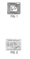
- An example of an etched foil radio frequency identification (RFID) tag is illustrated in FIG. 1 .
- Foil etching is wasteful and poses environmental disadvantages since most of the material, typically aluminum or copper, is discarded.
- Etch masks have been produced using ink jet printing devices.
- Ink jet printing devices are known in the art, and thus extensive description of such devices is not required herein.
- Phase change inks are desirable for ink jet printers because they remain in a solid phase at room temperature during shipping, long term storage, and the like.
- the problems associated with nozzle clogging as a result of ink evaporation with liquid ink jet inks are largely eliminated, thereby improving the reliability of the ink jet printing.
- the droplets solidify immediately upon contact with the substrate, so that migration of ink along the printing medium is prevented and dot quality is improved.
- Radiation curable inks generally comprise at least one curable monomer, a colorant, and a radiation activated initiator, specifically a photoinitiator, that initiates polymerization of curable components of the ink, specifically of the curable monomer.
- R 1 is an alkylene, arylene, arylalkylene, or alkylarylene group
- R 2 and R 2 ' each, independently of the other, are alkylene, arylene, arylalkylene, or alkylarylene groups
- R 3 and R 3 ' each, independently of the other, are either (a) photoinitiating groups, or (b) groups which are alkyl, aryl, arylalkyl, or alkylaryl groups, provided that at least one of R 3 and R 3 ' is a photoinitiating group
- X and X' each, independently of the other, is an oxygen atom or a group of the formula -NR 4 -, wherein R 4 is a hydrogen atom, an alkyl group, an aryl group, an arylalkyl group, or an alkylaryl group.
- phase change ink comprising a colorant, an initiator, and an ink vehicle, said ink vehicle comprising (a) at least one radically curable monomer compound, and (b) a compound of the formula
- R 1 is an alkylene, arylene, arylalkylene, or alkylarylene group
- R 2 and R 2 ' each, independently of the other, are alkylene, arylene, arylalkylene, or alkylarylene groups
- R 3 and R 3 ' each, independently of the other, are either (a) photoinitiating groups, or (b) groups which are alkyl, aryl, arylalkyl, or alkylaryl groups, provided that at least one of R 3 and R 3 ' is a photoinitiating group
- X and X' each, independently of the other, is an oxygen atom or a group of the formula -NR 4 -, wherein R 4 is a hydrogen atom, an alkyl group, an aryl group, an arylalkyl group, or an alkylaryl group.
- R 1 is an alkyl group having at least one ethylenic unsaturation, an arylalkyl group having at least one ethylenic unsaturation, or an alkylaryl group having at least one ethylenic unsaturation
- R 2 and R 3 each, independently of the others, are alkylene groups, arylene groups, arylalkylene groups, or alkylarylene groups
- n is an integer representing the number of repeat amide units and is at least 1, said process comprising: (a) reacting a diacid of the formula HOOC-R 2 -COOH
- R 1 and R 1 ' each, independently of the other, is an alkyl group having at least one ethylenic unsaturation, an arylalkyl group having at least one ethylenic unsaturation, or an alkylaryl group having at least one ethylenic unsaturation
- R 2 , R 2 ', and R 3 each, independently of the others, are alkylene groups, arylene groups, arylalkylene groups, or alkylarylene groups
- n is an integer representing the number of repeat amide units and is at least 1.
- U. S. Patent 6,742,884 of William S. Wong, et al. entitled “Apparatus for Printing Etch Masks Using Phase-Change Materials,” is directed to a method and system for masking a surface to be etched.
- a droplet source ejects droplets of a masking material for deposit on a thin-film or other substrate surface to be etched.
- the temperature of the thin-film or substrate surface is controlled such that the droplets rapidly freeze upon contact with the thin-film or substrate surface.
- the thin-film or substrate is then etched. After etching the masking material is removed. See Abstract of Wong. See also U. S. Patent 6,872,320 of William S. Wong, et al. , entitled “Method for Printing Etch Masks Using Phase-Change Materials,”.
- U. S. Patent 7,033,516 of William S. Wong, et al. entitled “Inexpensive Fabrication of Large-area Pixel Arrays For Displays And Sensors,” discloses a method for fabricating an array of electronic devices, typically a display or sensor.
- a droplet source ejects droplets of a masking material for deposit on a thin film or substrate surface to mask element of the array of electronic devices.
- the temperature of the thin-film or substrate surface is controlled such that the droplets rapidly freeze upon contact with the thin-film or substrate surface.
- the thin-film or substrate is then etched. After etching, the masking material is removed. See Abstract of Wong.
- FIG. 2 is a surface profile of a printed RFID antenna shown in Sangoi et al. illustrating printing irregularities therein. See Fig. 6 , page 517 of Sangoi et al.
- U. S. Patent 20040160465 discloses a method of preparing conductive structures on a substrate by printing radiation curable phase change material in a pattern of fillable channels on the surface of the substrate, curing the phase change material and depositing a conductive material in the fillable channels.
- a need remains for an improved system and method suitable for preparing conductive structures.
- a need remains for preparing conductive structures using thermally stable molds or dams that can withstand the elevated temperatures required for annealing conductive ink.
- a need remains for an improved system and method for digitally preparing conductive structures.
- Described is a method for preparing conductive structures on a substrate comprising printing a radiation curable phase change gel marking material in a pattern of fillable channels on a surface of a substrate; curing the radiation curable phase change gel marking material; depositing a conductive material in the fillable channels; annealing the conductive material; and optionally, removing the radiation curable phase change gel marking material.
- a system for preparing conductive structures on a substrate comprising a radiation curable phase change gel marking material source to print the radiation curable phase change gel marking material in a pattern on a surface of a substrate wherein the pattern creates fillable channels; a curing device for curing the radiation curable phase change gel marking material; a conductive material source to deposit the conductive material in the fillable channels; a heat source for annealing the conductive material; and optionally, a device for removing the radiation curable phase change gel marking material.
- Figure 1 is an illustration of an etched foil radio frequency identification tag.
- Figure 2 is a surface metrology image showing surface irregularities on a portion of a printed radio frequency identification antenna.
- Figure 3 is a block diagram illustrating an embodiment of the present system for preparing conductive structures using radiation curable phase change gel marking material.
- Figure 4 is a flow diagram illustrating an embodiment of the present method for preparing conductive structures using radiation curable phase change gel marking material.
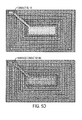
- FIGS. 5A through 5D illustrate an embodiment of the present method wherein the digital dam functions as an insulating layer.
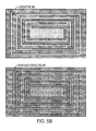
- Figure 6 is a micrograph of a solid ink dam prepared by jetting solid black ink in a pattern on a substrate.
- Figure 7 is a micrograph of a device prepared by jetting a printed dam pattern of solid black on a substrate, dispensing conductive ink in the dams, and annealing the conductive ink.
- the radiation curable phase change gel marking material is an ultraviolet curable phase gel ink or an electron beam radiation curable phase change gel ink.
- radiation curable phase change gel inks are provided as phase change ink marking materials used to prepare digital dams having a desired pattern. The dams are then filled with conductive material and annealed to form thick conductive metallic features, electronic circuitry, and electronic devices, including, but not limited to, radio frequency identification (RFID) tags.
- RFID radio frequency identification
- the radiation curable phase change gel ink marking materials have wide substrate latitude which allows the phase change ink digital dam pattern to be printed on any substrate that can withstand the subsequent annealing process.
- the present disclosure provides a system and method for preparation of conductive structures in one pass.
- the radiation curable phase change gel marking materials are comprised of an optional colorant, radiation curable monomers, prepolymers, and/or oligomers, a photoinitiator package, a reactive wax, and a gellant. Pigments or other functional particles may be optionally included depending on the desired application.
- the rheological properties of the radiation curable phase change marking materials can be tuned to achieve robust jetting at elevated temperatures (for example, in embodiments, about 85 °C) and a degree of mechanical stability (for example, in embodiments, about 10 5 to about 10 6 centipoise) at ambient substrate temperatures (i.e. room temperature).
- the increase in viscosity to from about 10 5 to from about 10 6 centipoise allows the digital dam patterned structure to be built up.
- the structures Before curing, the structures may have a consistency resembling tooth paste and can be altered by touch. After curing, the structures are quite robust.
- the gel nature of the radiation curable phase change gel marking materials at room temperature prevents spread or migration of the printed droplet and allows for facile build-up of the digital dam patterned structures. Due to the radiation curable nature of this material, the printed object can be cured by any suitable or desired method, such as by exposure to ultraviolet radiation, thermal radiation, or electron beam radiation at any point in the fabrication process resulting in robust patterned features with a high degree of mechanical strength.
- the radiation curable phase change gel marking materials herein can be cured after completion of each separate printing pass used to form the digital dam if desired. Alternately, in the interest of time, the inks can be cured upon completion of all printing passes.
- the method herein comprises printing one pass or a printing a number of successive passes of the radiation curable phase change gel marking material to form digital dams having a selected pattern.
- the dam pattern template can be prepared using computer software and the printheads programmed to print along the x axis and y axis in one or more printing passes.
- the pattern of fillable channels (or digital dams) is created using from about one to about five printing passes.
- the pattern of fillable channels is created using one printing pass.
- patterns of virtually any design can be created, from a micro-sized scale to a macro-sized scale and can include simple patterns to patterns having complex geometries.
- the radiation curable phase change gel ink jet marking materials and method herein further advantageously provide a noncontact, additive process (as opposed to subtractive process such as etching) providing the built-in ability to deliver metered amounts of the present ink materials to a precise location in time and space.
- phase change ink marking materials employed herein can comprise any suitable curable monomer or oligomer.
- suitable materials include radiation curable monomer compounds, such as acrylate and methacrylate monomer compounds, which are suitable for use as phase change ink carriers.
- relatively nonpolar acrylate and methacrylate monomers include (but are not limited to) isobornyl acrylate, isobornyl methacrylate, lauryl acrylate, lauryl methacrylate, isodecylacrylate, isodecylmethacrylate, caprolactone acrylate, 2-phenoxyethyl acrylate, isooctylacrylate, isooctylmethacrylate, butyl acrylate, and the like, as well as mixtures and combinations thereof.
- multifunctional acrylate and methacrylate monomers and oligomers can be included in the phase change ink carrier as reactive diluents and as materials that can increase the crosslink density of the cured image, thereby enhancing the toughness of the cured images.
- Different monomer and oligomers can also be added to tune the plasticity or elasticity of the cured objects.
- Suitable multifunctional acrylate and methacrylate monomers and oligomers include (but are not limited to) pentaerythritol tetraacrylate, pentaerythritol tetramethacrylate, 1,2-ethylene glycol diacrylate, 1,2-ethylene glycol dimethacrylate, 1,6-hexanediol diacrylate, 1,6-hexanediol dimethacrylate, 1,12-dodecanol diacrylate, 1,12-dodecanol dimethacrylate, tris(2-hydroxy ethyl) isocyanurate triacrylate, propoxylated neopentyl glycol diacrylate (available from Sartomer Co. Inc.
- SR 9003 hexanediol diacrylate
- tripropylene glycol diacrylate dipropylene glycol diacrylate
- amine modified polyether acrylates available as PO 83 F, LR 8869, and/or LR 8889 (all available from BASF Corporation)
- trimethylolpropane triacrylate glycerol propoxylate triacrylate
- dipentaerythritol pentaacrylate dipentaerythritol hexaacrylate
- ethoxylated pentaerythritol tetraacrylate available from Sartomer Co. Inc. as SR 494
- the reactive diluent is added in any desired or effective amount, in one embodiment at least about 1 percent by weight of the carrier, and in another embodiment at least about 35 percent by weight of the carrier, and in one embodiment no more than about 80 percent by weight of the carrier, and in another embodiment no more than about 70 percent by weight of the carrier, although the amount of diluent can be outside of these ranges.
- the phase change ink marking materials contain at least one compound that can exhibit gel-like behavior in that it undergoes a relatively sharp increase in viscosity over a relatively narrow temperature range when dissolved in a liquid such as those compounds that behave as curable monomers when exposed to radiation such as ultraviolet light.
- a liquid curable monomer is a propoxylated neopentyl glycol diacrylate such as SR9003®, commercially available from Sartomer Co. Inc.
- some compounds as disclosed herein undergo a change in viscosity of at least about 10 3 centipoise, in another embodiment at least about 10 5 centipoise, and in yet another embodiment at least about 10 6 centipoise over a temperature range of in one embodiment at least about 30°C, in another embodiment at least about 10°C, and in yet another embodiment at least about 5°C, although the viscosity change and temperature range can be outside of these ranges, and compounds that do not undergo changes within these ranges are also included herein.
- At least some embodiments of the compounds disclosed herein can form a semi-solid gel at a first temperature.
- this temperature is below the specific temperature at which the ink is jetted.
- the semi-solid gel phase is a physical gel that exists as a dynamic equilibrium comprising one or more solid gellant molecules and a liquid solvent.
- the semi-solid gel phase is a dynamic networked assembly of molecular components held together by noncovalent interactions such as hydrogen bonding, Van der Waals interactions, aromatic non-bonding interactions, ionic or coordination bonding, London dispersion forces, or the like, which, upon stimulation by physical forces, such as temperature, mechanical agitation, or the like, or chemical forces, such as pH, ionic strength, or the like, can undergo reversible transitions from liquid to semi-solid state at the macroscopic level.
- the solutions containing the gellant molecules exhibit a thermally reversible transition between the semi-solid gel state and the liquid state when the temperature is varied above or below the gel point of the solution. This reversible cycle of transitioning between semi-solid gel phase and liquid phase can be repeated many times in the solution formulation.
- the ink vehicles disclosed herein can comprise any suitable photoinitiator.
- suitable photoinitiator examples include, but are not limited to, Irgacure® 127, Irgacure® 379, and Irgacure® 819, all commercially available from Ciba Specialty Chemicals, among others.
- Suitable initiators include (but are not limited to) benzophenones, benzyl ketones, monomeric hydroxyl ketones, polymeric hydroxyl ketones, ⁇ -alkoxy benzyl ketones, ⁇ -amino ketones, acyl phosphine oxides, metallocenes, benzoin ethers, benzil ketals, ⁇ -hydroxyalkylphenones, ⁇ -aminoalkylphenones, acylphosphine photoinitiators sold under the trade designations of Irgacure® and Darocur® available from Ciba Specialty Chemicals, and the like.
- 1-hydroxy-cyclohexylphenylketone benzophenone, 2-benzyl-2-(dimethylamino)-1-(4-(4-morphorlinyl)phenyl)-1-butanone, 2-methyl-1-(4-methylthio)phenyl-2-(4-morphorlinyl)-1-propanone, diphenyl-(2,4,6-trimethylbenzoyl) phosphine oxide, phenyl bis(2,4,6-trimethylbenzoyl) phosphine oxide, benzyl-dimethylketal, isopropylthioxanthone, 2,4,6-trimethylbenzoyldiphenylphosphine oxide (available as BASF LUCIRIN® TPO), 2,4,6-trimethylbenzoylethoxyphenylphosphine oxide (available as BASF LUCIRIN® TPO-L), bis(2,4,6-trimethylbenzoyl)-phenyl-phosphine oxide
- the phase change inks can also contain an amine synergist, which are co-initiators which can donate a hydrogen atom to a photoinitiator and thereby form a radical species that initiates polymerization, and can also consume dissolved oxygen, which inhibits free-radical polymerization, thereby increasing the speed of polymerization.
- amine synergists include (but are not limited to) ethyl-4-dimethylaminobenzoate, 2-ethylhexyl-4-dimethylaminobenzoate, and the like, as well as mixtures thereof.
- Initiators for inks disclosed herein can absorb radiation at any desired or effective wavelength, in one embodiment at least about 200 nanometers, and in one embodiment no more than about 560 nanometers, and in another embodiment no more than about 420 nanometers, although the wavelength can be outside of these ranges.
- the photoinitiator is present in the phase change ink in any desired or effective amount, in one embodiment at least about 0.5 percent by weight of the ink composition, and in another embodiment at least about 1 percent by weight of the ink composition, and in one embodiment no more than about 15 percent by weight of the ink composition, and in another embodiment no more than about 10 percent by weight of the ink composition, although the amount can be outside of these ranges.
- the reactive wax comprises a curable wax component that is miscible with the other components and that will polymerize with the curable monomer to form a polymer. Inclusion of the wax promotes an increase in viscosity of the ink as it cools from the jetting temperature.
- Suitable examples of waxes include, but are not limited to, those that are functionalized with curable groups.
- the curable groups may include, but are not limited to, acrylate, methacrylate, alkene, allylic ether, epoxide and oxetane.
- These waxes can be synthesized by the reaction of a wax equipped with a transformable functional group, such as carboxylic acid or hydroxyl.
- Suitable examples of hydroxyl-terminated polyethylene waxes that may be functionalized with a curable group include, but are not limited to, mixtures of carbon chains with the structure CH 3 -(CH 2 ) n -CH 2 OH, where there is a mixture of chain lengths, n, where the average chain length is in selected embodiments in the range of about 16 to about 50, and linear low molecular weight polyethylene, of similar average chain length.
- Suitable examples of such waxes include, but are not limited to, UNILIN® 350, UNFLIN® 425, UNILIN® 550 and UNILIN® 700 with Mn approximately equal to 375, 460, 550 and 700 g/mol, respectively. All of these waxes are commercially available from Baker-Petrolite.
- Guerbet alcohols characterized as 2,2-dialkyl-1-ethanols, are also suitable compounds. Specific embodiments of Guerbet alcohols include those containing 16 to 36 carbons, many of which are commercially available from Jarchem Industries Inc., Newark, NJ. In embodiments, PRIPOL® 2033 is selected, PRIPOL® 2033 being a C-36 dimer diol mixture including isomers of the formula
- Suitable examples of carboxylic acid-terminated polyethylene waxes that may be functionalized with a curable group include, but are not limited to, mixtures of carbon chains with the structure CH 3 -(CH 2 ) n -COOH, where there is a mixture of chain lengths, n, where the average chain length is in selected embodiments in the range of about 16 to about 50, and linear low molecular weight polyethylene, of similar average chain length.
- Suitable examples of such waxes include, but are not limited to, UNICID® 350, UNICID® 425, UNICID® 550 and UNICID® 700 with Mn equal to approximately 390, 475, 565 and 720 g/mol, respectively.
- Guerbet acids characterized as 2,2-dialkyl ethanoic acids, are also suitable compounds.
- Selected Guerbet acids include those containing 16 to 36 carbons, many of which are commercially available from Jarchem Industries Inc., Newark, NJ.
- PRIPOL® 1009 C-36 dimer acid mixture including isomers of the formula
- the optional curable wax is included in the ink in an amount of from, for example, about 1 to about 25% by weight of the ink, or from about 2 to about 20% by weight of the ink, or from about 2.5 to about 15% by weight of the ink, although the amounts can be outside of these ranges.
- the curable monomer or prepolymer and curable wax together can form more than about 50% by weight of the ink, or at least 70% by weight of the ink, or at least 80% by weight of the ink, although not limited.
- any suitable gellant can be used for the ink vehicles disclosed herein.
- a gellant such as described in U. S. Patent Publication 20070120910, published May 31, 2007 , entitled “Phase Change Inks Containing Photoinitiator With Phase Change Properties and Gellant Affinity,” with the named inventors Peter G. Odell, Eniko Toma, and Jennifer L. Belelie, can be used, wherein the gellant is a compound of the formula
- R 1 is:
- R 2 and R 2 ' each, independently of the other, are:
- R 3 and R 3 ' each, independently of the other, are either:
- R 3 and R 3 ' is a photoinitiating group
- X and X' each, independently of the other, is an oxygen atom or a group of the formula -NR 4 -, wherein R 4 is:
- R 2 and R 2 ' are the same as each other; in another specific embodiment, R 2 and R 2 ' are different from each other. In one specific embodiment, R 3 and R 3 ' are the same as each other; in another specific embodiment, R 3 and R 3 ' are different from each other.
- R 2 and R 2 ' are each groups of the formula -C 34 H 56+a - and are branched alkylene groups which may include unsaturations and cyclic groups, wherein a is an integer of 0, 1, 2, 3, 4, 5, 6, 7, 8, 9, 10, 11, or 12, including (but not limited to) isomers of the formula
- R 1 is an ethylene (-CH 2 CH 2 -) group.
- R 3 and R 3 ' are both
- the compound is of the formula
- -C 34 H 56+a - represents a branched alkylene group which may include unsaturations and cyclic groups, wherein a is an integer of 0, 1, 2, 3, 4, 5, 6, 7, 8, 9, 10, 11, or 12, including (but not limited to) isomers of the formula
- -C 34 H 56+a - represents a branched alkylene group which may include unsaturations and cyclic groups, wherein a is an integer of 0, 1, 2, 3, 4, 5, 6, 7, 8, 9, 10, 11, or 12 and wherein m is an integer, including but not limited to embodiments wherein m is 2, including (but not limited to) isomers of the formula
- -C 34 H 56+a - represents a branched alkylene group which may include unsaturations and cyclic groups, wherein a is an integer of 0, 1, 2, 3, 4, 5, 6, 7, 8, 9, 10, 11, or 12 and wherein n is an integer, including but not limited to embodiments wherein n is 2 and wherein n is 5, including (but not limited to) isomers of the formula
- -C 34 H 56+a - represents a branched alkylene group which may include unsaturations and cyclic groups, wherein a is an integer of 0, 1, 2, 3, 4, 5, 6, 7, 8, 9, 10, 11, or 12 and wherein p is an integer, including but not limited to embodiments wherein p is 2 and wherein p is 3, including (but not limited to) isomers of the formula
- -C 34 H 56+a - represents a branched alkylene group which may include unsaturations and cyclic groups, wherein a is an integer of 0, 1, 2, 3, 4, 5, 6, 7, 8, 9, 10, 11, or 12 and wherein q is an integer, including but not limited to embodiments wherein q is 2 and wherein q is 3, including (but not limited to) isomers of the formula
- -C 34 H 56+a - represents a branched alkylene group which may include unsaturations and cyclic groups, wherein a is an integer of 0, 1, 2, 3, 4, 5, 6, 7, 8, 9, 10, 11, or 12 and wherein r is an integer, including but not limited to embodiments wherein r is 2 and wherein r is 3, including (but not limited to) isomers of the formula
- gellants herein can comprise materials disclosed U. S. Patent Publication 20070123606, published May 31, 2007 , entitled “Phase Change Inks Containing Curable Amide Gellant Compounds,” with the named inventors Eniko Toma, Jennifer L. Belelie, and Peter G. Odell, including a compound of the formula
- R 1 and R 1 ' each, independently of the other, is an alkyl group having at least one ethylenic unsaturation, an arylalkyl group having at least one ethylenic unsaturation, or an alkylaryl group having at least one ethylenic unsaturation
- R 2 , R 2 ', and R 3 each, independently of the others, are alkylene groups, arylene groups, arylalkylene groups, or alkylarylene groups
- n is an integer representing the number of repeat amide units and is at least 1.
- the gellant compounds as disclosed herein can be prepared by any desired or effective method.
- gellants can be prepared as described in U. S. Patent 7,259,275 , entitled “Method for Preparing Curable Amide Gellant Compounds,” with the named inventors Jennifer L. Belelie, Adela Goredema, Peter G. Odell, and Eniko Toma, which describes a process for preparing a compound of the formula
- R 1 is an alkyl group having at least one ethylenic unsaturation, an arylalkyl group having at least one ethylenic unsaturation, or an alkylaryl group having at least one ethylenic unsaturation
- R 2 and R 3 each, independently of the others, are alkylene groups, arylene groups, arylalkylene groups, or alkylarylene groups
- n is an integer representing the number of repeat amide units and is at least 1, said process comprising: (a) reacting a diacid of the formula HOOC-R 2 -COOH
- a colorant is included in the in the radiation curable phase change gel ink marking materials in any desired amount, for example from about 0.5 to about 75% by weight of the marking material, for example from about 1 to about 50% or from about 1 to about 25%, by weight of the marking material.
- any suitable colorant can be used in embodiments herein, including dyes, pigments, or combinations thereof.
- examples may include any dye or pigment capable of being dispersed or dissolved in the vehicle.
- suitable pigments include, for example, Paliogen Violet 5100 (BASF); Paliogen Violet 5890 (BASF); Heliogen Green L8730 (BASF); Lithol Scarlet D3700 (BASF); SUNFAST® Blue 15:4 (Sun Chemical 249-0592); HOSTAPERM Blue B2G-D (Clariant); Permanent Red P-F7RK; HOSTAPERM Violet BL (Clariant); Lithol Scarlet 4440 (BASF); Bon Red C (Dominion Color Company); Oracet Pink RF (Ciba); Paliogen Red 3871 K (BASF); SUNFAST ® Blue 15:3 (Sun Chemical 249-1284); Paliogen Red 3340 (BASF); SUNFAST ® Carbazole Violet 23 (Sun Chemical 246-1670); Lithol Fast
- Suitable dyes include Usharect Blue 86 (Direct Blue 86), available from Ushanti Color; Intralite Turquoise 8GL (Direct Blue 86), available from Classic Dyestuffs; Chemictive Brilliant Red 7BH (Reactive Red 4), available from Chemiequip; Levafix Black EB, available from Bayer; Reactron Red H8B (Reactive Red 31), available from Atlas Dye-Chem; D&C Red #28 (Acid Red 92), available from Warner-Jenkinson; Direct Brilliant Pink B, available from Global Colors; Acid Tartrazine, available from Metrochem Industries; Cartasol Yellow 6GF Clariant; Carta Blue 2GL, available from Clariant; and the like.
- Example solvent dyes include spirit soluble dyes such as Neozapon Red 492 (BASF); Orasol Red G (Ciba); Direct Brilliant Pink B (Global Colors); Aizen Spilon Red C-BH (Hodogaya Chemical); Kayanol Red 3BL (Nippon Kayaku); Spirit Fast Yellow 3G; Aizen Spilon Yellow C-GNH (Hodogaya Chemical); Cartasol Brilliant Yellow 4GF (Clariant); Pergasol Yellow CGP (Ciba); Orasol Black RLP (Ciba); Savinyl Black RLS (Clariant); Morfast Black Conc.
- spirit soluble dyes such as Neozapon Red 492 (BASF); Orasol Red G (Ciba); Direct Brilliant Pink B (Global Colors); Aizen Spilon Red C-BH (Hodogaya Chemical); Kayanol Red 3BL (Nippon Kayaku); Spirit Fast Yellow 3G; Aizen Spilon Yellow C-GNH (Hodogaya Chemical); Carta
- the radiation curable phase change gel inks herein can also optionally contain an antioxidant.
- the optional antioxidants can protect the images from oxidation and can also protect the ink components from oxidation during the heating portion of the ink preparation process.
- suitable antioxidant stabilizers include (but are not limited to) NAUGARD® 524, NAUGARD® 635, NAUGARD® A, NAUGARD® I-403, and NAUGARD® 959, commercially available from Crompton Corporation, Middlebury, CT; IRGANOX® 1010 and IRGASTAB® UV 10, commercially available from Ciba Specialty Chemicals; GENORAD 16 and GENORAD 40 commercially available from Rahn AG, Zurich, Switzerland, and the like, as well as mixtures thereof.
- the optional antioxidant is present in the ink in any desired or effective amount, in one embodiment at least about 0.01 percent by weight of the ink carrier, in another embodiment at least about 0.1 percent by weight of the ink carrier, and in yet another embodiment at least about 1 percent by weight of the ink carrier, and in one embodiment no more than about 20 percent by weight of the ink carrier, in another embodiment no more than about 5 percent by weight of the ink carrier, and in yet another embodiment no more than about 3 percent by weight of the ink carrier, although the amount can be outside of these ranges.
- the radiation curable phase change gel inks can also, if desired, contain additives to take advantage of the known functionality associated with such additives.
- additives may include, for example, defoamers, slip and leveling agents, pigment dispersants, surfactants, and the like, as well as mixtures thereof.
- the inks can also include additional monomeric or polymeric materials as desired.
- curable describes, for example, a material that may be cured via polymerization, including for example free radical routes, and/or in which polymerization is photoinitiated though use of a radiation-sensitive photoinitiator.
- radiation-curable refers, for example, to all forms of curing upon exposure to a radiation source, including light and heat sources and including in the presence or absence of initiators.
- Exemplary radiation-curing routes include, but are not limited to, curing using ultraviolet (UV) light, for example having a wavelength of 200-400 nm or more rarely visible light, optionally in the presence of photoinitiators and/or sensitizers, curing using electron-beam radiation, optionally in the absence of photoinitiators, curing using thermal curing, in the presence or absence of high-temperature thermal initiators (and which may be largely inactive at the jetting temperature), and appropriate combinations thereof.
- UV ultraviolet
- curing of the ink can be effected by exposure of the ink image to actinic radiation at any desired or effective wavelength, in one embodiment at least about 200 nanometers, and one embodiment no more than about 480 nanometers, although the wavelength can be outside of these ranges.
- Exposure to actinic radiation can be for any desired or effective period of time, in one embodiment for at least about 0.2 second, in another embodiment for at least about 1 second, and in yet another embodiment for at least about 5 seconds, and in one embodiment for no more than about 30 seconds, and in another embodiment for no more than about 15 seconds, although the exposure period can be outside of these ranges.
- viscosity refers to a complex viscosity, which is the typical measurement provided by a mechanical rheometer that is capable of subjecting a sample to a steady shear strain or a small amplitude sinusoidal deformation.
- the shear strain is applied by the operator to the motor and the sample deformation (torque) is measured by the transducer.
- examples of such instruments are the Rheometrics Fluid Rheometer RFS3 or the ARES mechanical spectrometer, both made by Rheometrics, a division of TA Instruments.
- a controlled-stress instrument where the shear stress is applied and the resultant strain is measured, may be used.
- rheometers examples include the majority of the current rheometers, the main manufacturers being Anton Parr GmbH, Bohlin Instruments, a division of Malvern Instruments, ATS Rheosystems and TA Instruments.
- a rheometer provides a periodic measurement of viscosity at various plate rotation frequencies, ⁇ , rather than the transient measurement of, for instance, a capillary viscometer.
- the reciprocating plate rheometer is able to measure both the in phase and out of phase fluid response to stress or displacement.
- a viscometer that can measure only the transient measurement of, for instance, a capillary or shear viscosity, such as those made by Brookfield Engineering Laboratories or Cannon Instrument Company can also be used.
- the ink compositions generally have melt viscosities at the jetting temperature (in one embodiment no lower than about 50°C, in another embodiment no lower than about 60°C, and in yet another embodiment no lower than about 70°C, and in one embodiment no higher than about 120°C, and in another embodiment no higher than about 110°C, although the jetting temperature can be outside of these ranges) in one embodiment of no more than about 30 centipoise, in another embodiment of no more than about 20 centipoise, and in yet another embodiment of no more than about 15 centipoise, and in one embodiment of no less than about 2 centipoise, in another embodiment of no less than about 5 centipoise, and in yet another embodiment of no less than about 7 centipoise, although the melt viscosity can be outside of these ranges.
- the inks are jetted at low temperatures, in particular at temperatures below about 110°C, in one embodiment from about 40°C to about 110°C, in another embodiment from about 50°C to about 110°C, and in yet another embodiment from about 60°C to about 90°C, although the jetting temperature can be outside of these ranges.
- the conventional use of temperature differential between the jetted ink and the substrate upon which the ink is jetted to effect a rapid phase change in the ink i.e., from liquid to solid
- the gellant can thus be used to effect a rapid viscosity increase in the jetted ink upon the substrate.
- jetted ink droplets can be pinned into position on a receiving substrate that is maintained at a temperature cooler than the ink jetting temperature of the ink through the action of a phase change transition in which the ink undergoes a significant viscosity change from a liquid state to a gel state (or semi-solid state).
- the temperature at which the ink forms the gel state is any temperature below the jetting temperature of the ink, in one embodiment any temperature that is about 5°C or more below the jetting temperature of the ink.
- the gel state can be formed at a temperature of at least about 25°C, and in another embodiment at a temperature of at least about 30°C, and in one embodiment of no more than about 100°C, in another embodiment of no more than about 70°C, and in yet another embodiment of no more than about 50°C, although the temperature can be outside of these ranges.
- a rapid and large increase in ink viscosity occurs upon cooling from the jetting temperature, at which the ink is in a liquid state, to the gel temperature, at which the ink is in the gel state.
- the viscosity increase is in one specific embodiment at least a 10 2.5 -fold increase in viscosity.
- the ultra-violet curable phase change marking materials can be prepared by any desired or suitable method.
- the ink ingredients can be mixed together, followed by heating, to a temperature in one embodiment of at least about 80°C, and in one embodiment of no more than about 120°C, although the temperature can be outside of these ranges, and stirring until a homogeneous ink composition is obtained, followed by cooling the ink to ambient temperature (typically from about 20°C to about 25°C).
- the inks are gels at ambient temperature.
- the dams are filled with conductive material and the conductive material is annealed to form an electronic structure on the substrate.
- the digital dams are removed.
- a section of the digital dam acts as insulator, enabling the formation of a conductive overpass without creating a short circuit with the underlying conductive trace. This is especially useful for creating capacitor layers for RFID tags, for example.
- the radiation curable phase change gel ink can be printed with topographical 'hills' and 'valleys' that can serve to 'shape' the flow of the conductive ink in order to create insulating layers.
- Figures 5A through 5B illustrate a series of plates showing an embodiment where the digital dam behaves as an insulating layer.
- a channel is created by deposition of an ultraviolet curable gel phase change ink dam (top plate) in a desired pattern followed by curing (bottom plate).
- Conductive ink is then deposited in the dam created by the ultraviolet curable gel phase change ink dam and annealed, Figure 5B , top plate and bottom plate, respectively.
- a subsequent layer (or layers) of ultraviolet curable phase change gel ink is deposited to create a dam overly having holes or vias and a contoured well for conductive ink to flow as desired, as shown in Figure 5C , top plate.
- the dam overlay ultraviolet curable phase change gel ink is then cured, as shown in Figure 5C , bottom plate.
- Conductive ink is then deposited, Figure 5D (top plate) and annealed Figure 5D (bottom plate) and this process can be repeated as desired to create additional circuitry.
- the conductive material can comprise any suitable material including, but not limited to, gold, silver, platinum, palladium, nickel, copper, cobalt, indium, tin, zinc, titanium, chromium, tantalum, tungsten, iron, rhodium, iridium, ruthenium, osmium, and lead.
- Further examples include nanoparticle ink material, for example wherein a nanoparticles composition comprising a metal which exhibits a low bulk resistivity such as, e.g., a bulk resistivity of less than about 15 micro- ⁇ cm, e.g., less than about 10 micro- Q cm, or less than about 5 micro- Q cm.
- Non-limiting examples of metals for use in nanoparticle ink materials include transition metals as well as main group metals such as, e.g., silver, gold, copper, nickel, cobalt, palladium, platinum, indium, tin, zinc, titanium, chromium, tantalum, tungsten, iron, rhodium, iridium, ruthenium, osmium, and lead.
- transition metals as well as main group metals such as, e.g., silver, gold, copper, nickel, cobalt, palladium, platinum, indium, tin, zinc, titanium, chromium, tantalum, tungsten, iron, rhodium, iridium, ruthenium, osmium, and lead.
- the conductive material comprises a nanoparticles ink comprising gold, silver, platinum, palladium, nickel, copper, cobalt, indium, tin, zinc, titanium, chromium, tantalum, tungsten, iron, rhodium, iridium, ruthenium, osmium, or lead.
- the conductive material can comprise, in embodiments, metal nanoparticles compositions disclosed in U. S. Patent Publication 20060189113 of Karel Vanheusden et al., Published August 24, 2006 ,.
- the conductive material can comprise metal nanoparticles having a core-shell structure.
- the conductive material can comprise, in embodiments, metal nanoparticles compositions disclosed in U. S. Patent Publication 20070212562 of In-Keun Shim et al., Published September 13, 2007 .
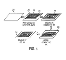
- FIG. 1 shows a system 100 for creating a substrate 102 having a conductive structure thereon.
- An ultra-violet curable phase change marking material source 104 such as an ink jet printer, is provided for printing a pattern of fillable channels or dams on the substrate 102.
- Any suitable substrate can be employed including plain papers such as XEROX® 4024 papers, XEROX® Image Series papers, Courtland 4024 DP paper, ruled notebook paper, bond paper, silica coated papers such as Sharp Company silica coated paper, JuJo paper, HAMMERMILL LASERPRINT® paper, and the like, glossy coated papers such as XEROX® Digital Color Gloss, Sappi Warren Papers LUSTROGLOSS®, and the like, transparency materials, fabrics, textile products, plastics, polymeric films, inorganic substrates such as metals, glass, and wood, as well as meltable or dissolvable substrates, such as waxes or salts, in the case of removable supports for free standing objects, and the like.
- plain papers such as XEROX® 4024 papers, XEROX® Image Series papers, Courtland 4024 DP paper, ruled notebook paper, bond paper, silica coated papers such as Sharp Company silica coated paper, JuJo paper, HAMMERMILL LASER
- any desired printing system can be employed for patterning the digital dams including systems suitable for preparing three-dimensional objects, such as a solid object printer.
- the printer can comprise a thermal ink jet printer, piezoelectric ink jet printer, acoustic ink jet printer, thermal transfer printer, gravure printer, electrostatographic printing methods, and the like.
- the printer comprises a piezoelectric ink jet printing apparatus.
- the printer described in U. S. Patent Publication 20080218540 of Gabriel Iftime, et al., published September 11, 2008 entirety, is employed.
- the ink jet printing apparatus described therein includes at least an ink jet print head and a print region surface toward which ink is jetted from the ink jet print head, wherein a height distance between the ink jet print head and the print region surface is adjustable.
- the ink jet print head is adjustable in spacing with respect to the print region surface so as to permit the ink jet print head to be moved from the a first position for regular height printing to a second height distance that is greater than (that is, the spacing between the ink jet print head and the print region surface is greater than) the first height distance.
- the second height distance is not fixed, and can be varied as necessary for a given printing. Moreover, the second height distance can itself be changed during a printing, as necessary. For example, it may be desirable to adjust the height distance from the first position to a second position as an image is built-up by the ink jet print head, and then as the image continues to be built-up, to adjust the ink jet print head from the second position to a third position in which the spacing from the print region surface is even further increased, and so on as necessary to complete build-up of the object.
- the printer 104 includes an x, y, z movable substrate stage.
- the printhead or target stage is movable in three dimensions, x, y, and z, enabling the preparation of a pattern of any desired size and configuration.
- multiple passes of the print head can be used to prepare channels by depositing successive layers of ink so that the pattern has a desired print height and geometry.
- the ultra-violet curable phase change marking material is printed to form a pattern of fillable channels having a channel depth of from about 1 to about 50 micrometers, although the depth can be outside of this range.
- the pattern of fillable channels is creating using from about 1 to about 5 printing passes, although not limited.
- Computer control of the ink jet print head or heads is employed to deposit the appropriate amount and/or layers of ink in the desired pattern so as to obtain the pattern with the desired print heights and overall geometries therein.
- Curing device 106 is employed for curing the printed substrate by exposing the printed substrate to UV curable light.
- Any suitable curing device can be used, for example, a UV Fusion LC-6B Benchtop Conveyor equipped with UV Fusion Light Hammer 6 Ultraviolet Lamp System employing a "D" bulb, although not limited.
- the channels can be filled with the conductive material using any suitable method such as by immersing the patterned substrate in a conductive material or by printing the conductive material.
- the conductive ink is deposited by printing the conductive ink using a single printing pass or using multiple printing passes.
- conductive ink source 108 deposits conductive material into the fillable channels.
- the conductive ink source can comprise a printer or any other device suitable for disposing the conductive material into the channels such as a doctor blade or wiper.
- the conductive ink can also be depositing in a separate printing operation, or by an analog process such as with a flood coater.
- Annealing device 110 is employed to anneal the deposited conductive ink to create a substrate having patterned conductive structure 116. Any suitable annealing device can be used, such as a hot plate or an oven.
- the ultra-violet curable phase change marking material can be removed, if desired.
- Any suitable device or method can be used to remove the ultra-violet curable phase change marking material.
- oven 112 can be used to burn off the ultra-violet curable phase change marking material from the prepared substrate 116.
- a wash station 114 can be used to wash off the ultra-violet curable phase change marking material with a solvent wash that is inert to the conductive marking material.
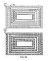
- FIG. 4 is a flow diagram illustrating the present method for preparing conductive structures using phase change marking material.
- substrate 200 is printed with a pattern 202 of fillable channels 204 formed by printing ultra-violet curable gellant phase change marking material thereon.
- the printed substrate 200 is immersed in conductive ink providing filled channels 206.
- the conductive ink is annealed as shown at block 208.
- the ultra-violet curable phase change marking material is removed.
- a solid ink dam was prepared by jetting solid black ink (Phaser® 8860 black ink available from Xerox® Corporation) in a pattern on Xerox Durapaper® paper using a Phaser® 8400 solid ink printer, jetting at 112°C and 24kHz.
- Figure 6 is a micrograph of the printed dam. A copper nanoparticle ink was dispensed within the dam in a single pass using a micropipette.
- the copper nanoparticle ink was annealed on a hot plate (Super-Nuova Digital hotplate, from Thermo Scientific) at 150 °C for 15 minutes providing a conductive structure having a 10 ohm resistance measured using an Omega 880 handheld digital multimeter.
- FIG. 7 is a micrograph of the annealed ink.
- a cyan ultra-violet curable phase change gellant ink A is prepared in accordance with the present disclosure as follows.
- An ultra-violet curable phase change gellant ink is prepared containing 7.5 percent by weight curable amide gellant as described in Example VIII of U. S. Patent 7,279,587 , 5 percent by weight Unilin 350® acrylate wax prepared as described in U. S.
- Patent Publication 2007120925 5 percent by weight pentafunctional acrylate monomer (SR 399LV® dipentaerythritol pentaacrylate available from Sartomer Co., Inc.), 52.8 percent by weight difunctional acrylate monomer (propoxylated neopentyl glycol diacrylate SR 9003® available from Sartomer Co., Inc.), 3 percent by weight IRGACURE® 379 photoinitiator (obtained from Ciba Specialty Chemicals), 1 percent by weight IRGACURE® 819 photoinitiator (obtained from Ciba Specialty Chemicals), 3.5 percent by weight IRGACURE® 127 photoinitiator (obtained from Ciba Specialty Chemicals), 2 percent by weight DAROCUR® ITX photoinitiator (obtained from Ciba Specialty Chemicals) 0.2 percent by weight UV stabilizer (IRGASTAB® UV10, obtained from Ciba Specialty Chemicals), and 20 percent by weight cyan pigment dis
- a UV curable ink dam is prepared by jetting the ultra-violet curable cyan gellant ink A in a pattern on Xerox Durapaper® taped to the drum of a modified Phaser® 8400 printer, at a temperature of 85°C, and a jetting frequency of 24kHz.
- the final dam thickness after 7 passes is approximately 70 micrometers.
- the Durapaper® is removed from the drum, and the printed dam is cured by passing through a Fusions UV Lighthammer® available from Fusions UV Systems, Inc., equipped with a 600W mercury D-bulb at a conveyor belt speed of 10fpm.
- a soluble silver precursor ink (Inktec® IJP-010, from InkTec Corporation) is applied to the dam using a micropipette. Through capillary action, the ink is drawn into the channels of the dam. The excess ink is wiped off, and, the dam containing the ink is heated to 120°C for 15 minutes to anneal the ink, forming a continuous conductive trace.
- the measured sheet resistance of the conductive area is 32.3 ohms/sq, measured using a CPS Resistivity Test Fixture fitted with a C4S 4-Point Probe Head (from Cascade Microtech Inc.) connected to a Keithley 236 source measure unit digital multimeter
- a clear ultra-violet curable phase change gellant ink composition B is prepared in accordance with the present disclosure as follows.
- An ultra-violet curable phase change gellant ink is prepared containing 7.5 percent by weight curable amide gellant as described in Example VIII of U. S. Patent 7,279,587 , 5 percent by weight Unilin 350® acrylate wax prepared as described in U. S.
- Patent Publication 2007120925 5 percent by weight pentafunctional acrylate monomer (SR 399LV® dipentaerythritol pentaacrylate available from Sartomer Co., Inc.), 77.8 percent by weight difunctional acrylate monomer (propoxylated neopentyl glycol diacrylate SR 9003® available from Sartomer Co., Inc.), 1 percent by weight IRGACURE® 819 photoinitiator (obtained from Ciba Specialty Chemicals), 3.5 percent by weight IRGACURE® 127 photoinitiator (obtained from Ciba Specialty Chemicals), and 0.2 percent by weight UV stabilizer (IRGASTAB® UV10, obtained from Ciba Specialty Chemicals. All of the components are stirred together at 90°C for 1 hour.
- pentafunctional acrylate monomer SR 399LV® dipentaerythritol pentaacrylate available from Sartomer Co., Inc.
- difunctional acrylate monomer prop
- An ultra-violet curable ink dam is prepared by jetting the ultra-violet curable clear gel ink B in a pattern on Xerox Durapaper® taped to the drum of a modified Phaser® 8400 printer, at a temperature of 85°C, and a jetting frequency of 24kHz.
- the final dam thickness after 7 passes is approximately 70 micrometers.
- the Durapaper® is removed from the drum, and the printed dam is cured by passing through a Fusions UV Lighthammer® available from Fusions UV Systems, Inc., equipped with a 600W mercury D-bulb at a conveyor belt speed of 10fpm.
- a soluble silver precursor ink (Inktec® IJP-010, from InkTec Corporation) is applied to the dam using a micropipette. Through capillary action, the ink is drawn into the channels of the dam. The excess ink is wiped off and the dam containing the ink is heated to 120°C for 15 minutes to anneal the ink, forming a continuous conductive trace.
- the measured sheet resistance of the conductive area is 30.1 ohms/sq, measured using a CPS Resistivity Test Fixture fitted with a C4S 4-Point Probe Head (from Cascade Microtech, Inc.) connected to a Keithley 236 source measure unit digital multimeter
Landscapes
- Chemical & Material Sciences (AREA)
- Engineering & Computer Science (AREA)
- Life Sciences & Earth Sciences (AREA)
- Materials Engineering (AREA)
- Wood Science & Technology (AREA)
- Organic Chemistry (AREA)
- Manufacturing & Machinery (AREA)
- Microelectronics & Electronic Packaging (AREA)
- Inks, Pencil-Leads, Or Crayons (AREA)
- Ink Jet Recording Methods And Recording Media Thereof (AREA)
- Manufacturing Of Printed Wiring (AREA)
- Macromonomer-Based Addition Polymer (AREA)
- Manufacturing Cores, Coils, And Magnets (AREA)
- Manufacturing Of Electric Cables (AREA)
Applications Claiming Priority (1)
| Application Number | Priority Date | Filing Date | Title |
|---|---|---|---|
| US12/489,638 US20100323102A1 (en) | 2009-06-23 | 2009-06-23 | System and Method for Preparing Conductive Structures Using Radiation Curable Phase Change Gel Inks |
Publications (3)
| Publication Number | Publication Date |
|---|---|
| EP2267478A2 EP2267478A2 (en) | 2010-12-29 |
| EP2267478A3 EP2267478A3 (en) | 2011-02-02 |
| EP2267478B1 true EP2267478B1 (en) | 2012-08-22 |
Family
ID=42932150
Family Applications (1)
| Application Number | Title | Priority Date | Filing Date |
|---|---|---|---|
| EP10166277A Not-in-force EP2267478B1 (en) | 2009-06-23 | 2010-06-17 | System and method for preparing conductive structures using radiation curable phase change gel inks |
Country Status (6)
Families Citing this family (25)
| Publication number | Priority date | Publication date | Assignee | Title |
|---|---|---|---|---|
| US8827391B2 (en) * | 2007-05-23 | 2014-09-09 | Xerox Corporation | Concurrently digitally printing/marking an image with a circuit |
| US8652574B2 (en) * | 2010-01-19 | 2014-02-18 | Xerox Corporation | Ink compositions |
| US8361562B2 (en) | 2010-01-19 | 2013-01-29 | Xerox Corporation | Ink compositions |
| US9649811B2 (en) * | 2011-04-17 | 2017-05-16 | Stratasys Ltd. | System and method for additive manufacturing of an object |
| US8581000B2 (en) * | 2011-06-06 | 2013-11-12 | Xerox Corporation | Process for preparing amide gellant compounds with aromatic end groups |
| US8635761B2 (en) | 2011-09-19 | 2014-01-28 | Xerox Corporation | System and method for formation of electrical conductors on a substrate |
| US9511582B2 (en) | 2012-07-30 | 2016-12-06 | Eastman Kodak Company | Ink formulations for flexographic printing of high-resolution conducting patterns |
| GB2520747C (en) * | 2013-11-29 | 2020-03-18 | Pragmatic Printing Ltd | Antenna and apparatus comprising antenna |
| EP3090609B1 (en) * | 2014-01-02 | 2017-06-28 | Philips Lighting Holding B.V. | Method for manufacturing a non-planar printed circuit board assembly |
| JP6303656B2 (ja) * | 2014-03-14 | 2018-04-04 | コニカミノルタ株式会社 | ゾルゲル相転移型インクジェットインクを用いたインクジェット記録方法 |
| WO2015199711A1 (en) * | 2014-06-27 | 2015-12-30 | Hewlett-Packard Development Company, L.P. | Radio frequency identification capsule |
| US20160009930A1 (en) * | 2014-07-09 | 2016-01-14 | Patrick Pagani | Radio frequency indentification (rfid) ink |
| KR101556909B1 (ko) * | 2014-07-31 | 2015-10-02 | 주식회사 밀다 | 밀고 당기는 모티스락 |
| US10462909B2 (en) * | 2014-11-14 | 2019-10-29 | Fuji Corporation | Wiring board manufacturing method and wiring board manufacturing device |
| US10174205B2 (en) * | 2015-10-19 | 2019-01-08 | Xerox Corporation | Printing process |
| US10308827B2 (en) | 2015-10-30 | 2019-06-04 | Xerox Corporation | Ink jet ink compositions for digital manufacturing of transparent objects |
| WO2018147835A1 (en) | 2017-02-07 | 2018-08-16 | Hewlett-Packard Development Company, L.P. | Fluidic conductive trace based radio-frequency identification |
| DE102017217847A1 (de) * | 2017-10-06 | 2019-04-11 | Rohde & Schwarz Gmbh & Co. Kg | Verfahren zum Herstellen eines teilweise hochleitfähig beschichteten Bauteils und Verwendung eines Tintenstrahldruckers |
| CN107864595A (zh) * | 2017-11-15 | 2018-03-30 | 深圳市迈安热控科技有限公司 | 热管传导散热装置 |
| US20200031040A1 (en) * | 2018-07-24 | 2020-01-30 | Xerox Corporation | Printing process and system |
| US10821658B2 (en) * | 2018-07-24 | 2020-11-03 | Xerox Corporation | Conductive three-dimensional articles |
| US20200102468A1 (en) * | 2018-10-02 | 2020-04-02 | Xerox Corporation | Dielectric ink composition |
| US10577515B1 (en) * | 2018-10-02 | 2020-03-03 | Xerox Corporation | Dielectric ink composition |
| CN113173004B (zh) * | 2021-04-26 | 2022-05-06 | 中国农业大学 | 一种导电微结构的制备方法和系统 |
| WO2023042159A1 (en) * | 2021-09-16 | 2023-03-23 | Sml Brand Identification Solutions Limited | Fabric-based rfid tags and methods of manufacture |
Family Cites Families (19)
| Publication number | Priority date | Publication date | Assignee | Title |
|---|---|---|---|---|
| GB0030095D0 (en) * | 2000-12-09 | 2001-01-24 | Xaar Technology Ltd | Method of ink jet printing |
| JP3625196B2 (ja) * | 2000-12-28 | 2005-03-02 | セイコーエプソン株式会社 | Rfidタグの形成方法、rfidタグの形成装置、スピーカの形成方法、およびスピーカの形成装置 |
| US6742884B2 (en) * | 2001-04-19 | 2004-06-01 | Xerox Corporation | Apparatus for printing etch masks using phase-change materials |
| US6872320B2 (en) * | 2001-04-19 | 2005-03-29 | Xerox Corporation | Method for printing etch masks using phase-change materials |
| US20060159838A1 (en) * | 2005-01-14 | 2006-07-20 | Cabot Corporation | Controlling ink migration during the formation of printable electronic features |
| US6911385B1 (en) * | 2002-08-22 | 2005-06-28 | Kovio, Inc. | Interface layer for the fabrication of electronic devices |
| WO2006076611A2 (en) * | 2005-01-14 | 2006-07-20 | Cabot Corporation | Production of metal nanoparticles |
| US7259275B2 (en) * | 2005-11-30 | 2007-08-21 | Xerox Corporation | Method for preparing curable amide gellant compounds |
| US7271284B2 (en) * | 2005-11-30 | 2007-09-18 | Xerox Corporation | Process for making curable amide gellant compounds |
| US7276614B2 (en) * | 2005-11-30 | 2007-10-02 | Xerox Corporation | Curable amide gellant compounds |
| US7625956B2 (en) * | 2005-11-30 | 2009-12-01 | Xerox Corporation | Phase change inks containing photoinitiator with phase change properties and gellant affinity |
| US7279587B2 (en) * | 2005-11-30 | 2007-10-09 | Xerox Corporation | Photoinitiator with phase change properties and gellant affinity |
| US7559639B2 (en) | 2005-11-30 | 2009-07-14 | Xerox Corporation | Radiation curable ink containing a curable wax |
| US7714040B2 (en) * | 2005-11-30 | 2010-05-11 | Xerox Corporation | Phase change inks containing curable amide gellant compounds |
| US7820731B2 (en) * | 2005-12-15 | 2010-10-26 | Xerox Corporation | Radiation curable inks |
| KR100781586B1 (ko) * | 2006-02-24 | 2007-12-05 | 삼성전기주식회사 | 코어-셀 구조의 금속 나노입자 및 이의 제조방법 |
| JP2008103641A (ja) * | 2006-10-20 | 2008-05-01 | Asahi Kasei Chemicals Corp | インクジェット印刷用被印刷基材の製造方法 |
| US8061791B2 (en) * | 2007-03-07 | 2011-11-22 | Xerox Corporation | Dual printer for regular and raised print |
| US7812064B2 (en) * | 2007-08-07 | 2010-10-12 | Xerox Corporation | Phase change ink compositions |
-
2009
- 2009-06-23 US US12/489,638 patent/US20100323102A1/en not_active Abandoned
-
2010
- 2010-06-16 CA CA2708056A patent/CA2708056C/en not_active Expired - Fee Related
- 2010-06-16 JP JP2010136835A patent/JP2011009743A/ja active Pending
- 2010-06-17 EP EP10166277A patent/EP2267478B1/en not_active Not-in-force
- 2010-06-22 KR KR1020100059128A patent/KR20100138799A/ko not_active Withdrawn
- 2010-06-23 CN CN2010102113985A patent/CN101932201A/zh active Pending
Also Published As
| Publication number | Publication date |
|---|---|
| US20100323102A1 (en) | 2010-12-23 |
| EP2267478A2 (en) | 2010-12-29 |
| CA2708056C (en) | 2014-01-14 |
| JP2011009743A (ja) | 2011-01-13 |
| EP2267478A3 (en) | 2011-02-02 |
| CA2708056A1 (en) | 2010-12-23 |
| KR20100138799A (ko) | 2010-12-31 |
| CN101932201A (zh) | 2010-12-29 |
Similar Documents
| Publication | Publication Date | Title |
|---|---|---|
| EP2267478B1 (en) | System and method for preparing conductive structures using radiation curable phase change gel inks | |
| EP2161312B1 (en) | Ultra-Violet Curable Gellant Inks for Three-Dimensional Printing and Digital Fabrication Applications | |
| EP2161315B1 (en) | Ultra-violet curable gellant inks for creating tactile text and images for packaging applications | |
| EP2161314B1 (en) | Ultra-violet curable gellant inks for tactile and regular print applications as security features for signature and document authentication | |
| US9012527B2 (en) | Curable compositions for three-dimensional printing | |
| CA2676889C (en) | Ultra-violet curable gellant inks for braille, raised print, and regular print applications | |
| EP2256170B1 (en) | Tunable fluorescent UV curable gel inks containing fluorescent monomers for food packaging applications | |
| US7887176B2 (en) | Imaging on flexible packaging substrates | |
| US8142557B2 (en) | Radiation curable ink containing gellant and radiation curable wax | |
| US7531582B2 (en) | Radiation curable phase change inks containing curable epoxy-polyamide composite gellants | |
| US7905948B2 (en) | Phase change ink compositions | |
| EP2223976B1 (en) | Method of forming images using curable ink with gellant | |
| US20120282448A1 (en) | Methods for fabricating three-dimensional objects | |
| US20080204538A1 (en) | Printing on corrugated substrates | |
| US20110243629A1 (en) | Process For Preparing Braille Images Using Inline Digital Coating | |
| US10738204B2 (en) | Printing process for preparing controlled scattering effects | |
| US8507584B2 (en) | Phase change inks containing amide gellant compounds with aromatic end groups |
Legal Events
| Date | Code | Title | Description |
|---|---|---|---|
| PUAI | Public reference made under article 153(3) epc to a published international application that has entered the european phase |
Free format text: ORIGINAL CODE: 0009012 |
|
| AK | Designated contracting states |
Kind code of ref document: A2 Designated state(s): AL AT BE BG CH CY CZ DE DK EE ES FI FR GB GR HR HU IE IS IT LI LT LU LV MC MK MT NL NO PL PT RO SE SI SK SM TR |
|
| AX | Request for extension of the european patent |
Extension state: BA ME RS |
|
| PUAL | Search report despatched |
Free format text: ORIGINAL CODE: 0009013 |
|
| AK | Designated contracting states |
Kind code of ref document: A3 Designated state(s): AL AT BE BG CH CY CZ DE DK EE ES FI FR GB GR HR HU IE IS IT LI LT LU LV MC MK MT NL NO PL PT RO SE SI SK SM TR |
|
| AX | Request for extension of the european patent |
Extension state: BA ME RS |
|
| 17P | Request for examination filed |
Effective date: 20110802 |
|
| REG | Reference to a national code |
Ref country code: DE Ref legal event code: R079 Ref document number: 602010002410 Country of ref document: DE Free format text: PREVIOUS MAIN CLASS: G01S0013750000 Ipc: H05K0003120000 |
|
| GRAP | Despatch of communication of intention to grant a patent |
Free format text: ORIGINAL CODE: EPIDOSNIGR1 |
|
| RIC1 | Information provided on ipc code assigned before grant |
Ipc: G01S 13/75 20060101AFI20111220BHEP Ipc: H05K 3/10 20060101ALI20111220BHEP Ipc: H05K 3/12 20060101ALI20111220BHEP |
|
| RIC1 | Information provided on ipc code assigned before grant |
Ipc: H05K 3/12 20060101AFI20111223BHEP |
|
| GRAS | Grant fee paid |
Free format text: ORIGINAL CODE: EPIDOSNIGR3 |
|
| GRAA | (expected) grant |
Free format text: ORIGINAL CODE: 0009210 |
|
| AK | Designated contracting states |
Kind code of ref document: B1 Designated state(s): AL AT BE BG CH CY CZ DE DK EE ES FI FR GB GR HR HU IE IS IT LI LT LU LV MC MK MT NL NO PL PT RO SE SI SK SM TR |
|
| REG | Reference to a national code |
Ref country code: GB Ref legal event code: FG4D |
|
| REG | Reference to a national code |
Ref country code: CH Ref legal event code: EP |
|
| REG | Reference to a national code |
Ref country code: IE Ref legal event code: FG4D |
|
| REG | Reference to a national code |
Ref country code: AT Ref legal event code: REF Ref document number: 572520 Country of ref document: AT Kind code of ref document: T Effective date: 20120915 |
|
| REG | Reference to a national code |
Ref country code: DE Ref legal event code: R096 Ref document number: 602010002410 Country of ref document: DE Effective date: 20121018 |
|
| REG | Reference to a national code |
Ref country code: NL Ref legal event code: VDEP Effective date: 20120822 |
|
| REG | Reference to a national code |
Ref country code: AT Ref legal event code: MK05 Ref document number: 572520 Country of ref document: AT Kind code of ref document: T Effective date: 20120822 |
|
| REG | Reference to a national code |
Ref country code: LT Ref legal event code: MG4D Effective date: 20120822 |
|
| PG25 | Lapsed in a contracting state [announced via postgrant information from national office to epo] |
Ref country code: FI Free format text: LAPSE BECAUSE OF FAILURE TO SUBMIT A TRANSLATION OF THE DESCRIPTION OR TO PAY THE FEE WITHIN THE PRESCRIBED TIME-LIMIT Effective date: 20120822 Ref country code: IS Free format text: LAPSE BECAUSE OF FAILURE TO SUBMIT A TRANSLATION OF THE DESCRIPTION OR TO PAY THE FEE WITHIN THE PRESCRIBED TIME-LIMIT Effective date: 20121222 Ref country code: NO Free format text: LAPSE BECAUSE OF FAILURE TO SUBMIT A TRANSLATION OF THE DESCRIPTION OR TO PAY THE FEE WITHIN THE PRESCRIBED TIME-LIMIT Effective date: 20121122 Ref country code: LT Free format text: LAPSE BECAUSE OF FAILURE TO SUBMIT A TRANSLATION OF THE DESCRIPTION OR TO PAY THE FEE WITHIN THE PRESCRIBED TIME-LIMIT Effective date: 20120822 Ref country code: HR Free format text: LAPSE BECAUSE OF FAILURE TO SUBMIT A TRANSLATION OF THE DESCRIPTION OR TO PAY THE FEE WITHIN THE PRESCRIBED TIME-LIMIT Effective date: 20120822 Ref country code: AT Free format text: LAPSE BECAUSE OF FAILURE TO SUBMIT A TRANSLATION OF THE DESCRIPTION OR TO PAY THE FEE WITHIN THE PRESCRIBED TIME-LIMIT Effective date: 20120822 |
|
| PG25 | Lapsed in a contracting state [announced via postgrant information from national office to epo] |
Ref country code: SI Free format text: LAPSE BECAUSE OF FAILURE TO SUBMIT A TRANSLATION OF THE DESCRIPTION OR TO PAY THE FEE WITHIN THE PRESCRIBED TIME-LIMIT Effective date: 20120822 Ref country code: BE Free format text: LAPSE BECAUSE OF FAILURE TO SUBMIT A TRANSLATION OF THE DESCRIPTION OR TO PAY THE FEE WITHIN THE PRESCRIBED TIME-LIMIT Effective date: 20120822 Ref country code: SE Free format text: LAPSE BECAUSE OF FAILURE TO SUBMIT A TRANSLATION OF THE DESCRIPTION OR TO PAY THE FEE WITHIN THE PRESCRIBED TIME-LIMIT Effective date: 20120822 Ref country code: LV Free format text: LAPSE BECAUSE OF FAILURE TO SUBMIT A TRANSLATION OF THE DESCRIPTION OR TO PAY THE FEE WITHIN THE PRESCRIBED TIME-LIMIT Effective date: 20120822 Ref country code: GR Free format text: LAPSE BECAUSE OF FAILURE TO SUBMIT A TRANSLATION OF THE DESCRIPTION OR TO PAY THE FEE WITHIN THE PRESCRIBED TIME-LIMIT Effective date: 20121123 Ref country code: PT Free format text: LAPSE BECAUSE OF FAILURE TO SUBMIT A TRANSLATION OF THE DESCRIPTION OR TO PAY THE FEE WITHIN THE PRESCRIBED TIME-LIMIT Effective date: 20121224 |
|
| PG25 | Lapsed in a contracting state [announced via postgrant information from national office to epo] |
Ref country code: NL Free format text: LAPSE BECAUSE OF FAILURE TO SUBMIT A TRANSLATION OF THE DESCRIPTION OR TO PAY THE FEE WITHIN THE PRESCRIBED TIME-LIMIT Effective date: 20120822 |
|
| PG25 | Lapsed in a contracting state [announced via postgrant information from national office to epo] |
Ref country code: RO Free format text: LAPSE BECAUSE OF FAILURE TO SUBMIT A TRANSLATION OF THE DESCRIPTION OR TO PAY THE FEE WITHIN THE PRESCRIBED TIME-LIMIT Effective date: 20120822 Ref country code: EE Free format text: LAPSE BECAUSE OF FAILURE TO SUBMIT A TRANSLATION OF THE DESCRIPTION OR TO PAY THE FEE WITHIN THE PRESCRIBED TIME-LIMIT Effective date: 20120822 Ref country code: DK Free format text: LAPSE BECAUSE OF FAILURE TO SUBMIT A TRANSLATION OF THE DESCRIPTION OR TO PAY THE FEE WITHIN THE PRESCRIBED TIME-LIMIT Effective date: 20120822 Ref country code: CZ Free format text: LAPSE BECAUSE OF FAILURE TO SUBMIT A TRANSLATION OF THE DESCRIPTION OR TO PAY THE FEE WITHIN THE PRESCRIBED TIME-LIMIT Effective date: 20120822 Ref country code: ES Free format text: LAPSE BECAUSE OF FAILURE TO SUBMIT A TRANSLATION OF THE DESCRIPTION OR TO PAY THE FEE WITHIN THE PRESCRIBED TIME-LIMIT Effective date: 20121203 |
|
| PG25 | Lapsed in a contracting state [announced via postgrant information from national office to epo] |
Ref country code: SK Free format text: LAPSE BECAUSE OF FAILURE TO SUBMIT A TRANSLATION OF THE DESCRIPTION OR TO PAY THE FEE WITHIN THE PRESCRIBED TIME-LIMIT Effective date: 20120822 Ref country code: IT Free format text: LAPSE BECAUSE OF FAILURE TO SUBMIT A TRANSLATION OF THE DESCRIPTION OR TO PAY THE FEE WITHIN THE PRESCRIBED TIME-LIMIT Effective date: 20120822 Ref country code: PL Free format text: LAPSE BECAUSE OF FAILURE TO SUBMIT A TRANSLATION OF THE DESCRIPTION OR TO PAY THE FEE WITHIN THE PRESCRIBED TIME-LIMIT Effective date: 20120822 |
|
| PLBE | No opposition filed within time limit |
Free format text: ORIGINAL CODE: 0009261 |
|
| STAA | Information on the status of an ep patent application or granted ep patent |
Free format text: STATUS: NO OPPOSITION FILED WITHIN TIME LIMIT |
|
| 26N | No opposition filed |
Effective date: 20130523 |
|
| PG25 | Lapsed in a contracting state [announced via postgrant information from national office to epo] |
Ref country code: BG Free format text: LAPSE BECAUSE OF FAILURE TO SUBMIT A TRANSLATION OF THE DESCRIPTION OR TO PAY THE FEE WITHIN THE PRESCRIBED TIME-LIMIT Effective date: 20121122 |
|
| REG | Reference to a national code |
Ref country code: DE Ref legal event code: R097 Ref document number: 602010002410 Country of ref document: DE Effective date: 20130523 |
|
| PG25 | Lapsed in a contracting state [announced via postgrant information from national office to epo] |
Ref country code: CY Free format text: LAPSE BECAUSE OF FAILURE TO SUBMIT A TRANSLATION OF THE DESCRIPTION OR TO PAY THE FEE WITHIN THE PRESCRIBED TIME-LIMIT Effective date: 20120822 |
|
| PG25 | Lapsed in a contracting state [announced via postgrant information from national office to epo] |
Ref country code: MC Free format text: LAPSE BECAUSE OF FAILURE TO SUBMIT A TRANSLATION OF THE DESCRIPTION OR TO PAY THE FEE WITHIN THE PRESCRIBED TIME-LIMIT Effective date: 20120822 |
|
| REG | Reference to a national code |
Ref country code: IE Ref legal event code: MM4A |
|
| PG25 | Lapsed in a contracting state [announced via postgrant information from national office to epo] |
Ref country code: IE Free format text: LAPSE BECAUSE OF NON-PAYMENT OF DUE FEES Effective date: 20130617 |
|
| REG | Reference to a national code |
Ref country code: CH Ref legal event code: PL |
|
| PG25 | Lapsed in a contracting state [announced via postgrant information from national office to epo] |
Ref country code: MT Free format text: LAPSE BECAUSE OF FAILURE TO SUBMIT A TRANSLATION OF THE DESCRIPTION OR TO PAY THE FEE WITHIN THE PRESCRIBED TIME-LIMIT Effective date: 20120822 |
|
| PG25 | Lapsed in a contracting state [announced via postgrant information from national office to epo] |
Ref country code: CH Free format text: LAPSE BECAUSE OF NON-PAYMENT OF DUE FEES Effective date: 20140630 Ref country code: LI Free format text: LAPSE BECAUSE OF NON-PAYMENT OF DUE FEES Effective date: 20140630 |
|
| PG25 | Lapsed in a contracting state [announced via postgrant information from national office to epo] |
Ref country code: SM Free format text: LAPSE BECAUSE OF FAILURE TO SUBMIT A TRANSLATION OF THE DESCRIPTION OR TO PAY THE FEE WITHIN THE PRESCRIBED TIME-LIMIT Effective date: 20120822 |
|
| PG25 | Lapsed in a contracting state [announced via postgrant information from national office to epo] |
Ref country code: TR Free format text: LAPSE BECAUSE OF FAILURE TO SUBMIT A TRANSLATION OF THE DESCRIPTION OR TO PAY THE FEE WITHIN THE PRESCRIBED TIME-LIMIT Effective date: 20120822 |
|
| PG25 | Lapsed in a contracting state [announced via postgrant information from national office to epo] |
Ref country code: LU Free format text: LAPSE BECAUSE OF NON-PAYMENT OF DUE FEES Effective date: 20130617 Ref country code: MK Free format text: LAPSE BECAUSE OF FAILURE TO SUBMIT A TRANSLATION OF THE DESCRIPTION OR TO PAY THE FEE WITHIN THE PRESCRIBED TIME-LIMIT Effective date: 20120822 Ref country code: HU Free format text: LAPSE BECAUSE OF FAILURE TO SUBMIT A TRANSLATION OF THE DESCRIPTION OR TO PAY THE FEE WITHIN THE PRESCRIBED TIME-LIMIT; INVALID AB INITIO Effective date: 20100617 |
|
| REG | Reference to a national code |
Ref country code: FR Ref legal event code: PLFP Year of fee payment: 7 |
|
| REG | Reference to a national code |
Ref country code: FR Ref legal event code: PLFP Year of fee payment: 8 |
|
| REG | Reference to a national code |
Ref country code: FR Ref legal event code: PLFP Year of fee payment: 9 |
|
| PGFP | Annual fee paid to national office [announced via postgrant information from national office to epo] |
Ref country code: DE Payment date: 20180522 Year of fee payment: 9 |
|
| PGFP | Annual fee paid to national office [announced via postgrant information from national office to epo] |
Ref country code: FR Payment date: 20180525 Year of fee payment: 9 |
|
| PG25 | Lapsed in a contracting state [announced via postgrant information from national office to epo] |
Ref country code: AL Free format text: LAPSE BECAUSE OF FAILURE TO SUBMIT A TRANSLATION OF THE DESCRIPTION OR TO PAY THE FEE WITHIN THE PRESCRIBED TIME-LIMIT Effective date: 20120822 |
|
| PGFP | Annual fee paid to national office [announced via postgrant information from national office to epo] |
Ref country code: GB Payment date: 20180522 Year of fee payment: 9 |
|
| REG | Reference to a national code |
Ref country code: DE Ref legal event code: R119 Ref document number: 602010002410 Country of ref document: DE |
|
| GBPC | Gb: european patent ceased through non-payment of renewal fee |
Effective date: 20190617 |
|
| PG25 | Lapsed in a contracting state [announced via postgrant information from national office to epo] |
Ref country code: DE Free format text: LAPSE BECAUSE OF NON-PAYMENT OF DUE FEES Effective date: 20200101 Ref country code: GB Free format text: LAPSE BECAUSE OF NON-PAYMENT OF DUE FEES Effective date: 20190617 |
|
| PG25 | Lapsed in a contracting state [announced via postgrant information from national office to epo] |
Ref country code: FR Free format text: LAPSE BECAUSE OF NON-PAYMENT OF DUE FEES Effective date: 20190630 |