EP2264491B1 - Diffraktionsfilter nullter Ordnung und Herstellungsverfahren dafür - Google Patents
Diffraktionsfilter nullter Ordnung und Herstellungsverfahren dafür Download PDFInfo
- Publication number
- EP2264491B1 EP2264491B1 EP10165817.7A EP10165817A EP2264491B1 EP 2264491 B1 EP2264491 B1 EP 2264491B1 EP 10165817 A EP10165817 A EP 10165817A EP 2264491 B1 EP2264491 B1 EP 2264491B1
- Authority
- EP
- European Patent Office
- Prior art keywords
- index
- low
- matter
- zero
- layer
- Prior art date
- Legal status (The legal status is an assumption and is not a legal conclusion. Google has not performed a legal analysis and makes no representation as to the accuracy of the status listed.)
- Revoked
Links
- 238000000034 method Methods 0.000 title description 53
- 238000004519 manufacturing process Methods 0.000 title description 21
- 239000000463 material Substances 0.000 claims description 92
- 230000000694 effects Effects 0.000 claims description 13
- 239000002086 nanomaterial Substances 0.000 claims description 3
- 239000010410 layer Substances 0.000 description 95
- 239000000758 substrate Substances 0.000 description 40
- 239000002904 solvent Substances 0.000 description 32
- 238000000576 coating method Methods 0.000 description 26
- 239000011248 coating agent Substances 0.000 description 24
- 229920000642 polymer Polymers 0.000 description 23
- 230000003993 interaction Effects 0.000 description 16
- ZWEHNKRNPOVVGH-UHFFFAOYSA-N 2-Butanone Chemical compound CCC(C)=O ZWEHNKRNPOVVGH-UHFFFAOYSA-N 0.000 description 15
- -1 for example Substances 0.000 description 13
- 239000011368 organic material Substances 0.000 description 12
- 239000002105 nanoparticle Substances 0.000 description 11
- RTZKZFJDLAIYFH-UHFFFAOYSA-N Diethyl ether Chemical compound CCOCC RTZKZFJDLAIYFH-UHFFFAOYSA-N 0.000 description 10
- XEKOWRVHYACXOJ-UHFFFAOYSA-N Ethyl acetate Chemical compound CCOC(C)=O XEKOWRVHYACXOJ-UHFFFAOYSA-N 0.000 description 10
- 239000007787 solid Substances 0.000 description 10
- OKKJLVBELUTLKV-UHFFFAOYSA-N Methanol Chemical compound OC OKKJLVBELUTLKV-UHFFFAOYSA-N 0.000 description 9
- GWEVSGVZZGPLCZ-UHFFFAOYSA-N Titan oxide Chemical compound O=[Ti]=O GWEVSGVZZGPLCZ-UHFFFAOYSA-N 0.000 description 9
- 238000007639 printing Methods 0.000 description 9
- CSCPPACGZOOCGX-UHFFFAOYSA-N Acetone Chemical compound CC(C)=O CSCPPACGZOOCGX-UHFFFAOYSA-N 0.000 description 8
- HEDRZPFGACZZDS-UHFFFAOYSA-N Chloroform Chemical compound ClC(Cl)Cl HEDRZPFGACZZDS-UHFFFAOYSA-N 0.000 description 8
- LFQSCWFLJHTTHZ-UHFFFAOYSA-N Ethanol Chemical compound CCO LFQSCWFLJHTTHZ-UHFFFAOYSA-N 0.000 description 8
- YXFVVABEGXRONW-UHFFFAOYSA-N Toluene Chemical compound CC1=CC=CC=C1 YXFVVABEGXRONW-UHFFFAOYSA-N 0.000 description 8
- 238000000151 deposition Methods 0.000 description 8
- 238000004049 embossing Methods 0.000 description 8
- 239000011888 foil Substances 0.000 description 8
- VLKZOEOYAKHREP-UHFFFAOYSA-N n-Hexane Chemical compound CCCCCC VLKZOEOYAKHREP-UHFFFAOYSA-N 0.000 description 8
- 230000008569 process Effects 0.000 description 8
- 239000000020 Nitrocellulose Substances 0.000 description 7
- 230000008021 deposition Effects 0.000 description 7
- 239000011159 matrix material Substances 0.000 description 7
- 229920001220 nitrocellulos Polymers 0.000 description 7
- CXQXSVUQTKDNFP-UHFFFAOYSA-N octamethyltrisiloxane Chemical compound C[Si](C)(C)O[Si](C)(C)O[Si](C)(C)C CXQXSVUQTKDNFP-UHFFFAOYSA-N 0.000 description 7
- 239000004014 plasticizer Substances 0.000 description 7
- 229920002689 polyvinyl acetate Polymers 0.000 description 7
- SOGAXMICEFXMKE-UHFFFAOYSA-N Butylmethacrylate Chemical compound CCCCOC(=O)C(C)=C SOGAXMICEFXMKE-UHFFFAOYSA-N 0.000 description 6
- YMWUJEATGCHHMB-UHFFFAOYSA-N Dichloromethane Chemical compound ClCCl YMWUJEATGCHHMB-UHFFFAOYSA-N 0.000 description 6
- KFZMGEQAYNKOFK-UHFFFAOYSA-N Isopropanol Chemical compound CC(C)O KFZMGEQAYNKOFK-UHFFFAOYSA-N 0.000 description 6
- 239000012080 ambient air Substances 0.000 description 6
- 239000004205 dimethyl polysiloxane Substances 0.000 description 6
- 235000013870 dimethyl polysiloxane Nutrition 0.000 description 6
- 238000002156 mixing Methods 0.000 description 6
- 230000003287 optical effect Effects 0.000 description 6
- 238000004987 plasma desorption mass spectroscopy Methods 0.000 description 6
- 229920001490 poly(butyl methacrylate) polymer Polymers 0.000 description 6
- 229920000435 poly(dimethylsiloxane) Polymers 0.000 description 6
- 229920003229 poly(methyl methacrylate) Polymers 0.000 description 6
- 239000004926 polymethyl methacrylate Substances 0.000 description 6
- 230000008961 swelling Effects 0.000 description 6
- LRHPLDYGYMQRHN-UHFFFAOYSA-N N-Butanol Chemical compound CCCCO LRHPLDYGYMQRHN-UHFFFAOYSA-N 0.000 description 5
- 239000012790 adhesive layer Substances 0.000 description 5
- 238000007646 gravure printing Methods 0.000 description 5
- 229920002451 polyvinyl alcohol Polymers 0.000 description 5
- XLYOFNOQVPJJNP-UHFFFAOYSA-N water Substances O XLYOFNOQVPJJNP-UHFFFAOYSA-N 0.000 description 5
- IMNFDUFMRHMDMM-UHFFFAOYSA-N N-Heptane Chemical compound CCCCCCC IMNFDUFMRHMDMM-UHFFFAOYSA-N 0.000 description 4
- OFBQJSOFQDEBGM-UHFFFAOYSA-N Pentane Chemical compound CCCCC OFBQJSOFQDEBGM-UHFFFAOYSA-N 0.000 description 4
- 239000004793 Polystyrene Substances 0.000 description 4
- 239000004372 Polyvinyl alcohol Substances 0.000 description 4
- WYURNTSHIVDZCO-UHFFFAOYSA-N Tetrahydrofuran Chemical compound C1CCOC1 WYURNTSHIVDZCO-UHFFFAOYSA-N 0.000 description 4
- MVPPADPHJFYWMZ-UHFFFAOYSA-N chlorobenzene Chemical compound ClC1=CC=CC=C1 MVPPADPHJFYWMZ-UHFFFAOYSA-N 0.000 description 4
- 238000004132 cross linking Methods 0.000 description 4
- JHIVVAPYMSGYDF-UHFFFAOYSA-N cyclohexanone Chemical compound O=C1CCCCC1 JHIVVAPYMSGYDF-UHFFFAOYSA-N 0.000 description 4
- 239000000203 mixture Substances 0.000 description 4
- 230000003595 spectral effect Effects 0.000 description 4
- 239000000126 substance Substances 0.000 description 4
- 239000004408 titanium dioxide Substances 0.000 description 4
- WEVYAHXRMPXWCK-UHFFFAOYSA-N Acetonitrile Chemical compound CC#N WEVYAHXRMPXWCK-UHFFFAOYSA-N 0.000 description 3
- UHOVQNZJYSORNB-UHFFFAOYSA-N Benzene Chemical compound C1=CC=CC=C1 UHOVQNZJYSORNB-UHFFFAOYSA-N 0.000 description 3
- QGJOPFRUJISHPQ-UHFFFAOYSA-N Carbon disulfide Chemical compound S=C=S QGJOPFRUJISHPQ-UHFFFAOYSA-N 0.000 description 3
- XDTMQSROBMDMFD-UHFFFAOYSA-N Cyclohexane Chemical compound C1CCCCC1 XDTMQSROBMDMFD-UHFFFAOYSA-N 0.000 description 3
- LYCAIKOWRPUZTN-UHFFFAOYSA-N Ethylene glycol Chemical compound OCCO LYCAIKOWRPUZTN-UHFFFAOYSA-N 0.000 description 3
- 108010010803 Gelatin Proteins 0.000 description 3
- PEDCQBHIVMGVHV-UHFFFAOYSA-N Glycerine Chemical compound OCC(O)CO PEDCQBHIVMGVHV-UHFFFAOYSA-N 0.000 description 3
- ZMXDDKWLCZADIW-UHFFFAOYSA-N N,N-Dimethylformamide Chemical compound CN(C)C=O ZMXDDKWLCZADIW-UHFFFAOYSA-N 0.000 description 3
- CTQNGGLPUBDAKN-UHFFFAOYSA-N O-Xylene Chemical group CC1=CC=CC=C1C CTQNGGLPUBDAKN-UHFFFAOYSA-N 0.000 description 3
- URLKBWYHVLBVBO-UHFFFAOYSA-N Para-Xylene Chemical compound CC1=CC=C(C)C=C1 URLKBWYHVLBVBO-UHFFFAOYSA-N 0.000 description 3
- JFZHPFOXAAIUMB-UHFFFAOYSA-N Phenylethylmalonamide Chemical compound CCC(C(N)=O)(C(N)=O)C1=CC=CC=C1 JFZHPFOXAAIUMB-UHFFFAOYSA-N 0.000 description 3
- 238000004040 coloring Methods 0.000 description 3
- 238000009826 distribution Methods 0.000 description 3
- 239000010408 film Substances 0.000 description 3
- 239000008273 gelatin Substances 0.000 description 3
- 229920000159 gelatin Polymers 0.000 description 3
- 235000019322 gelatine Nutrition 0.000 description 3
- 235000011852 gelatine desserts Nutrition 0.000 description 3
- 239000007788 liquid Substances 0.000 description 3
- 239000002060 nanoflake Substances 0.000 description 3
- 229920001483 poly(ethyl methacrylate) polymer Polymers 0.000 description 3
- 229920000915 polyvinyl chloride Polymers 0.000 description 3
- VYPSYNLAJGMNEJ-UHFFFAOYSA-N silicon dioxide Inorganic materials O=[Si]=O VYPSYNLAJGMNEJ-UHFFFAOYSA-N 0.000 description 3
- VZGDMQKNWNREIO-UHFFFAOYSA-N tetrachloromethane Chemical compound ClC(Cl)(Cl)Cl VZGDMQKNWNREIO-UHFFFAOYSA-N 0.000 description 3
- 238000000411 transmission spectrum Methods 0.000 description 3
- RFFLAFLAYFXFSW-UHFFFAOYSA-N 1,2-dichlorobenzene Chemical compound ClC1=CC=CC=C1Cl RFFLAFLAYFXFSW-UHFFFAOYSA-N 0.000 description 2
- RYHBNJHYFVUHQT-UHFFFAOYSA-N 1,4-Dioxane Chemical compound C1COCCO1 RYHBNJHYFVUHQT-UHFFFAOYSA-N 0.000 description 2
- FFWSICBKRCICMR-UHFFFAOYSA-N 5-methyl-2-hexanone Chemical compound CC(C)CCC(C)=O FFWSICBKRCICMR-UHFFFAOYSA-N 0.000 description 2
- RGSFGYAAUTVSQA-UHFFFAOYSA-N Cyclopentane Chemical compound C1CCCC1 RGSFGYAAUTVSQA-UHFFFAOYSA-N 0.000 description 2
- IAZDPXIOMUYVGZ-UHFFFAOYSA-N Dimethylsulphoxide Chemical compound CS(C)=O IAZDPXIOMUYVGZ-UHFFFAOYSA-N 0.000 description 2
- ZHNUHDYFZUAESO-UHFFFAOYSA-N Formamide Chemical compound NC=O ZHNUHDYFZUAESO-UHFFFAOYSA-N 0.000 description 2
- NHTMVDHEPJAVLT-UHFFFAOYSA-N Isooctane Chemical compound CC(C)CC(C)(C)C NHTMVDHEPJAVLT-UHFFFAOYSA-N 0.000 description 2
- 229920003171 Poly (ethylene oxide) Polymers 0.000 description 2
- 239000004642 Polyimide Substances 0.000 description 2
- MCMNRKCIXSYSNV-UHFFFAOYSA-N Zirconium dioxide Chemical compound O=[Zr]=O MCMNRKCIXSYSNV-UHFFFAOYSA-N 0.000 description 2
- RDOXTESZEPMUJZ-UHFFFAOYSA-N anisole Chemical compound COC1=CC=CC=C1 RDOXTESZEPMUJZ-UHFFFAOYSA-N 0.000 description 2
- DKPFZGUDAPQIHT-UHFFFAOYSA-N butyl acetate Chemical compound CCCCOC(C)=O DKPFZGUDAPQIHT-UHFFFAOYSA-N 0.000 description 2
- 229950005499 carbon tetrachloride Drugs 0.000 description 2
- 239000002131 composite material Substances 0.000 description 2
- 229920001795 coordination polymer Polymers 0.000 description 2
- 230000008878 coupling Effects 0.000 description 2
- 238000010168 coupling process Methods 0.000 description 2
- 238000005859 coupling reaction Methods 0.000 description 2
- DIOQZVSQGTUSAI-UHFFFAOYSA-N decane Chemical compound CCCCCCCCCC DIOQZVSQGTUSAI-UHFFFAOYSA-N 0.000 description 2
- 230000001419 dependent effect Effects 0.000 description 2
- 238000004090 dissolution Methods 0.000 description 2
- 230000007613 environmental effect Effects 0.000 description 2
- 238000010438 heat treatment Methods 0.000 description 2
- ZXEKIIBDNHEJCQ-UHFFFAOYSA-N isobutanol Chemical compound CC(C)CO ZXEKIIBDNHEJCQ-UHFFFAOYSA-N 0.000 description 2
- 239000004922 lacquer Substances 0.000 description 2
- 239000011344 liquid material Substances 0.000 description 2
- 239000002245 particle Substances 0.000 description 2
- XNLICIUVMPYHGG-UHFFFAOYSA-N pentan-2-one Chemical compound CCCC(C)=O XNLICIUVMPYHGG-UHFFFAOYSA-N 0.000 description 2
- 239000000049 pigment Substances 0.000 description 2
- 229920000371 poly(diallyldimethylammonium chloride) polymer Polymers 0.000 description 2
- 229920001601 polyetherimide Polymers 0.000 description 2
- 229920001721 polyimide Polymers 0.000 description 2
- 229920002223 polystyrene Polymers 0.000 description 2
- 230000001902 propagating effect Effects 0.000 description 2
- BDERNNFJNOPAEC-UHFFFAOYSA-N propan-1-ol Chemical compound CCCO BDERNNFJNOPAEC-UHFFFAOYSA-N 0.000 description 2
- 239000012056 semi-solid material Substances 0.000 description 2
- 238000001228 spectrum Methods 0.000 description 2
- 229920002994 synthetic fiber Polymers 0.000 description 2
- 239000010409 thin film Substances 0.000 description 2
- 230000001131 transforming effect Effects 0.000 description 2
- 238000001771 vacuum deposition Methods 0.000 description 2
- 238000009834 vaporization Methods 0.000 description 2
- 230000008016 vaporization Effects 0.000 description 2
- AJDIZQLSFPQPEY-UHFFFAOYSA-N 1,1,2-Trichlorotrifluoroethane Chemical compound FC(F)(Cl)C(F)(Cl)Cl AJDIZQLSFPQPEY-UHFFFAOYSA-N 0.000 description 1
- WSLDOOZREJYCGB-UHFFFAOYSA-N 1,2-Dichloroethane Chemical compound ClCCCl WSLDOOZREJYCGB-UHFFFAOYSA-N 0.000 description 1
- VFWCMGCRMGJXDK-UHFFFAOYSA-N 1-chlorobutane Chemical compound CCCCCl VFWCMGCRMGJXDK-UHFFFAOYSA-N 0.000 description 1
- XNWFRZJHXBZDAG-UHFFFAOYSA-N 2-METHOXYETHANOL Chemical compound COCCO XNWFRZJHXBZDAG-UHFFFAOYSA-N 0.000 description 1
- PTTPXKJBFFKCEK-UHFFFAOYSA-N 2-Methyl-4-heptanone Chemical compound CC(C)CC(=O)CC(C)C PTTPXKJBFFKCEK-UHFFFAOYSA-N 0.000 description 1
- MMSGPUZNNKBAMN-UHFFFAOYSA-N 3-ethyl-4-hydroxyheptane-2,3,4-tricarboxylic acid Chemical compound CCC(C(O)=O)C(O)(C(O)=O)C(CC)(CC)C(O)=O MMSGPUZNNKBAMN-UHFFFAOYSA-N 0.000 description 1
- MKXAREWNUVZNTJ-UHFFFAOYSA-N 5-acetyl-7-butyl-6-hydroxyundecane-4,5,6-tricarboxylic acid Chemical compound CCCCC(CCCC)(C(O)=O)C(O)(C(O)=O)C(CCCC)(C(C)=O)C(O)=O MKXAREWNUVZNTJ-UHFFFAOYSA-N 0.000 description 1
- NIXOWILDQLNWCW-UHFFFAOYSA-M Acrylate Chemical compound [O-]C(=O)C=C NIXOWILDQLNWCW-UHFFFAOYSA-M 0.000 description 1
- 239000004923 Acrylic lacquer Substances 0.000 description 1
- ZFOZVQLOBQUTQQ-UHFFFAOYSA-N Citronensaeure-tributylester Natural products CCCCOC(=O)CC(O)(C(=O)OCCCC)CC(=O)OCCCC ZFOZVQLOBQUTQQ-UHFFFAOYSA-N 0.000 description 1
- ONKUXPIBXRRIDU-UHFFFAOYSA-N Diethyl decanedioate Chemical compound CCOC(=O)CCCCCCCCC(=O)OCC ONKUXPIBXRRIDU-UHFFFAOYSA-N 0.000 description 1
- ZAFNJMIOTHYJRJ-UHFFFAOYSA-N Diisopropyl ether Chemical compound CC(C)OC(C)C ZAFNJMIOTHYJRJ-UHFFFAOYSA-N 0.000 description 1
- NIQCNGHVCWTJSM-UHFFFAOYSA-N Dimethyl phthalate Chemical compound COC(=O)C1=CC=CC=C1C(=O)OC NIQCNGHVCWTJSM-UHFFFAOYSA-N 0.000 description 1
- 239000004593 Epoxy Substances 0.000 description 1
- JOYRKODLDBILNP-UHFFFAOYSA-N Ethyl urethane Chemical compound CCOC(N)=O JOYRKODLDBILNP-UHFFFAOYSA-N 0.000 description 1
- 229920000877 Melamine resin Polymers 0.000 description 1
- NTIZESTWPVYFNL-UHFFFAOYSA-N Methyl isobutyl ketone Chemical compound CC(C)CC(C)=O NTIZESTWPVYFNL-UHFFFAOYSA-N 0.000 description 1
- UIHCLUNTQKBZGK-UHFFFAOYSA-N Methyl isobutyl ketone Natural products CCC(C)C(C)=O UIHCLUNTQKBZGK-UHFFFAOYSA-N 0.000 description 1
- BZLVMXJERCGZMT-UHFFFAOYSA-N Methyl tert-butyl ether Chemical compound COC(C)(C)C BZLVMXJERCGZMT-UHFFFAOYSA-N 0.000 description 1
- FXHOOIRPVKKKFG-UHFFFAOYSA-N N,N-Dimethylacetamide Chemical compound CN(C)C(C)=O FXHOOIRPVKKKFG-UHFFFAOYSA-N 0.000 description 1
- SECXISVLQFMRJM-UHFFFAOYSA-N N-Methylpyrrolidone Chemical compound CN1CCCC1=O SECXISVLQFMRJM-UHFFFAOYSA-N 0.000 description 1
- 229920002302 Nylon 6,6 Polymers 0.000 description 1
- 239000004696 Poly ether ether ketone Substances 0.000 description 1
- XBDQKXXYIPTUBI-UHFFFAOYSA-M Propionate Chemical compound CCC([O-])=O XBDQKXXYIPTUBI-UHFFFAOYSA-M 0.000 description 1
- DNIAPMSPPWPWGF-UHFFFAOYSA-N Propylene glycol Chemical compound CC(O)CO DNIAPMSPPWPWGF-UHFFFAOYSA-N 0.000 description 1
- JUJWROOIHBZHMG-UHFFFAOYSA-N Pyridine Chemical compound C1=CC=NC=C1 JUJWROOIHBZHMG-UHFFFAOYSA-N 0.000 description 1
- XUIMIQQOPSSXEZ-UHFFFAOYSA-N Silicon Chemical compound [Si] XUIMIQQOPSSXEZ-UHFFFAOYSA-N 0.000 description 1
- 229910000831 Steel Inorganic materials 0.000 description 1
- RSWGJHLUYNHPMX-ONCXSQPRSA-N abietic acid Chemical compound C([C@@H]12)CC(C(C)C)=CC1=CC[C@@H]1[C@]2(C)CCC[C@@]1(C)C(O)=O RSWGJHLUYNHPMX-ONCXSQPRSA-N 0.000 description 1
- 238000010521 absorption reaction Methods 0.000 description 1
- KXKVLQRXCPHEJC-UHFFFAOYSA-N acetic acid trimethyl ester Natural products COC(C)=O KXKVLQRXCPHEJC-UHFFFAOYSA-N 0.000 description 1
- 239000002253 acid Substances 0.000 description 1
- 239000000853 adhesive Substances 0.000 description 1
- 230000001070 adhesive effect Effects 0.000 description 1
- 238000005054 agglomeration Methods 0.000 description 1
- 230000002776 aggregation Effects 0.000 description 1
- 239000003570 air Substances 0.000 description 1
- 229920000180 alkyd Polymers 0.000 description 1
- 229910052782 aluminium Inorganic materials 0.000 description 1
- PNEYBMLMFCGWSK-UHFFFAOYSA-N aluminium oxide Inorganic materials [O-2].[O-2].[O-2].[Al+3].[Al+3] PNEYBMLMFCGWSK-UHFFFAOYSA-N 0.000 description 1
- 238000010923 batch production Methods 0.000 description 1
- JUPQTSLXMOCDHR-UHFFFAOYSA-N benzene-1,4-diol;bis(4-fluorophenyl)methanone Chemical compound OC1=CC=C(O)C=C1.C1=CC(F)=CC=C1C(=O)C1=CC=C(F)C=C1 JUPQTSLXMOCDHR-UHFFFAOYSA-N 0.000 description 1
- 238000007664 blowing Methods 0.000 description 1
- 230000001680 brushing effect Effects 0.000 description 1
- DQXBYHZEEUGOBF-UHFFFAOYSA-N but-3-enoic acid;ethene Chemical compound C=C.OC(=O)CC=C DQXBYHZEEUGOBF-UHFFFAOYSA-N 0.000 description 1
- 229920002678 cellulose Polymers 0.000 description 1
- 239000001913 cellulose Substances 0.000 description 1
- KRKNYBCHXYNGOX-UHFFFAOYSA-N citric acid Substances OC(=O)CC(O)(C(O)=O)CC(O)=O KRKNYBCHXYNGOX-UHFFFAOYSA-N 0.000 description 1
- 229910052681 coesite Inorganic materials 0.000 description 1
- 239000003086 colorant Substances 0.000 description 1
- 230000000295 complement effect Effects 0.000 description 1
- 229910052802 copper Inorganic materials 0.000 description 1
- 229910052593 corundum Inorganic materials 0.000 description 1
- 229910052906 cristobalite Inorganic materials 0.000 description 1
- FLKPEMZONWLCSK-UHFFFAOYSA-N diethyl phthalate Chemical compound CCOC(=O)C1=CC=CC=C1C(=O)OCC FLKPEMZONWLCSK-UHFFFAOYSA-N 0.000 description 1
- JVSWJIKNEAIKJW-UHFFFAOYSA-N dimethyl-hexane Natural products CCCCCC(C)C JVSWJIKNEAIKJW-UHFFFAOYSA-N 0.000 description 1
- 229940113088 dimethylacetamide Drugs 0.000 description 1
- 238000007598 dipping method Methods 0.000 description 1
- 239000003814 drug Substances 0.000 description 1
- 239000005038 ethylene vinyl acetate Substances 0.000 description 1
- 238000007647 flexography Methods 0.000 description 1
- 229910052949 galena Inorganic materials 0.000 description 1
- 239000007789 gas Substances 0.000 description 1
- 239000011521 glass Substances 0.000 description 1
- DMEGYFMYUHOHGS-UHFFFAOYSA-N heptamethylene Natural products C1CCCCCC1 DMEGYFMYUHOHGS-UHFFFAOYSA-N 0.000 description 1
- 229920002100 high-refractive-index polymer Polymers 0.000 description 1
- 239000001257 hydrogen Substances 0.000 description 1
- 229910052739 hydrogen Inorganic materials 0.000 description 1
- 238000005286 illumination Methods 0.000 description 1
- 238000007641 inkjet printing Methods 0.000 description 1
- 229910052742 iron Inorganic materials 0.000 description 1
- 229940035429 isobutyl alcohol Drugs 0.000 description 1
- 239000012948 isocyanate Substances 0.000 description 1
- 150000002513 isocyanates Chemical class 0.000 description 1
- JMMWKPVZQRWMSS-UHFFFAOYSA-N isopropanol acetate Natural products CC(C)OC(C)=O JMMWKPVZQRWMSS-UHFFFAOYSA-N 0.000 description 1
- 229940011051 isopropyl acetate Drugs 0.000 description 1
- GWYFCOCPABKNJV-UHFFFAOYSA-N isovaleric acid Chemical compound CC(C)CC(O)=O GWYFCOCPABKNJV-UHFFFAOYSA-N 0.000 description 1
- JDSHMPZPIAZGSV-UHFFFAOYSA-N melamine Chemical compound NC1=NC(N)=NC(N)=N1 JDSHMPZPIAZGSV-UHFFFAOYSA-N 0.000 description 1
- UODXCYZDMHPIJE-UHFFFAOYSA-N menthanol Chemical compound CC1CCC(C(C)(C)O)CC1 UODXCYZDMHPIJE-UHFFFAOYSA-N 0.000 description 1
- 229910052751 metal Inorganic materials 0.000 description 1
- 239000002184 metal Substances 0.000 description 1
- 229910044991 metal oxide Inorganic materials 0.000 description 1
- 150000004706 metal oxides Chemical class 0.000 description 1
- UZKWTJUDCOPSNM-UHFFFAOYSA-N methoxybenzene Substances CCCCOC=C UZKWTJUDCOPSNM-UHFFFAOYSA-N 0.000 description 1
- YKYONYBAUNKHLG-UHFFFAOYSA-N n-Propyl acetate Natural products CCCOC(C)=O YKYONYBAUNKHLG-UHFFFAOYSA-N 0.000 description 1
- 229910052759 nickel Inorganic materials 0.000 description 1
- LYGJENNIWJXYER-UHFFFAOYSA-N nitromethane Chemical compound C[N+]([O-])=O LYGJENNIWJXYER-UHFFFAOYSA-N 0.000 description 1
- 229940078552 o-xylene Drugs 0.000 description 1
- TVMXDCGIABBOFY-UHFFFAOYSA-N octane Chemical compound CCCCCCCC TVMXDCGIABBOFY-UHFFFAOYSA-N 0.000 description 1
- 230000005693 optoelectronics Effects 0.000 description 1
- 239000000123 paper Substances 0.000 description 1
- 230000000737 periodic effect Effects 0.000 description 1
- 239000003208 petroleum Substances 0.000 description 1
- 230000000704 physical effect Effects 0.000 description 1
- 229920001643 poly(ether ketone) Polymers 0.000 description 1
- 229920001200 poly(ethylene-vinyl acetate) Polymers 0.000 description 1
- 229920006260 polyaryletherketone Polymers 0.000 description 1
- 229920000728 polyester Polymers 0.000 description 1
- 229920002530 polyetherether ketone Polymers 0.000 description 1
- 229920001155 polypropylene Polymers 0.000 description 1
- 239000004810 polytetrafluoroethylene Substances 0.000 description 1
- 229920001343 polytetrafluoroethylene Polymers 0.000 description 1
- 229920002635 polyurethane Polymers 0.000 description 1
- 239000004814 polyurethane Substances 0.000 description 1
- 239000011118 polyvinyl acetate Substances 0.000 description 1
- 230000001737 promoting effect Effects 0.000 description 1
- 229940090181 propyl acetate Drugs 0.000 description 1
- RUOJZAUFBMNUDX-UHFFFAOYSA-N propylene carbonate Chemical compound CC1COC(=O)O1 RUOJZAUFBMNUDX-UHFFFAOYSA-N 0.000 description 1
- 239000011241 protective layer Substances 0.000 description 1
- 239000010453 quartz Substances 0.000 description 1
- 230000001105 regulatory effect Effects 0.000 description 1
- 238000007761 roller coating Methods 0.000 description 1
- 238000007650 screen-printing Methods 0.000 description 1
- 238000000926 separation method Methods 0.000 description 1
- 229910052710 silicon Inorganic materials 0.000 description 1
- 239000010703 silicon Substances 0.000 description 1
- 239000000377 silicon dioxide Substances 0.000 description 1
- 239000011343 solid material Substances 0.000 description 1
- 238000007614 solvation Methods 0.000 description 1
- 238000005507 spraying Methods 0.000 description 1
- 238000003892 spreading Methods 0.000 description 1
- 230000007480 spreading Effects 0.000 description 1
- 230000003068 static effect Effects 0.000 description 1
- 239000010959 steel Substances 0.000 description 1
- 229910052682 stishovite Inorganic materials 0.000 description 1
- YLQBMQCUIZJEEH-UHFFFAOYSA-N tetrahydrofuran Natural products C=1C=COC=1 YLQBMQCUIZJEEH-UHFFFAOYSA-N 0.000 description 1
- 229920001169 thermoplastic Polymers 0.000 description 1
- 239000004416 thermosoftening plastic Substances 0.000 description 1
- 229910052718 tin Inorganic materials 0.000 description 1
- 229910052905 tridymite Inorganic materials 0.000 description 1
- NQPDZGIKBAWPEJ-UHFFFAOYSA-N valeric acid Chemical compound CCCCC(O)=O NQPDZGIKBAWPEJ-UHFFFAOYSA-N 0.000 description 1
- 235000012431 wafers Nutrition 0.000 description 1
- 238000005406 washing Methods 0.000 description 1
- 239000008096 xylene Substances 0.000 description 1
- 229910001845 yogo sapphire Inorganic materials 0.000 description 1
Images


Classifications
-
- G—PHYSICS
- G02—OPTICS
- G02B—OPTICAL ELEMENTS, SYSTEMS OR APPARATUS
- G02B5/00—Optical elements other than lenses
- G02B5/18—Diffraction gratings
- G02B5/1809—Diffraction gratings with pitch less than or comparable to the wavelength
-
- G—PHYSICS
- G02—OPTICS
- G02B—OPTICAL ELEMENTS, SYSTEMS OR APPARATUS
- G02B27/00—Optical systems or apparatus not provided for by any of the groups G02B1/00 - G02B26/00, G02B30/00
- G02B27/42—Diffraction optics, i.e. systems including a diffractive element being designed for providing a diffractive effect
- G02B27/44—Grating systems; Zone plate systems
-
- G—PHYSICS
- G02—OPTICS
- G02B—OPTICAL ELEMENTS, SYSTEMS OR APPARATUS
- G02B5/00—Optical elements other than lenses
- G02B5/18—Diffraction gratings
- G02B5/1847—Manufacturing methods
-
- B—PERFORMING OPERATIONS; TRANSPORTING
- B42—BOOKBINDING; ALBUMS; FILES; SPECIAL PRINTED MATTER
- B42D—BOOKS; BOOK COVERS; LOOSE LEAVES; PRINTED MATTER CHARACTERISED BY IDENTIFICATION OR SECURITY FEATURES; PRINTED MATTER OF SPECIAL FORMAT OR STYLE NOT OTHERWISE PROVIDED FOR; DEVICES FOR USE THEREWITH AND NOT OTHERWISE PROVIDED FOR; MOVABLE-STRIP WRITING OR READING APPARATUS
- B42D25/00—Information-bearing cards or sheet-like structures characterised by identification or security features; Manufacture thereof
- B42D25/20—Information-bearing cards or sheet-like structures characterised by identification or security features; Manufacture thereof characterised by a particular use or purpose
- B42D25/29—Securities; Bank notes
-
- B—PERFORMING OPERATIONS; TRANSPORTING
- B42—BOOKBINDING; ALBUMS; FILES; SPECIAL PRINTED MATTER
- B42D—BOOKS; BOOK COVERS; LOOSE LEAVES; PRINTED MATTER CHARACTERISED BY IDENTIFICATION OR SECURITY FEATURES; PRINTED MATTER OF SPECIAL FORMAT OR STYLE NOT OTHERWISE PROVIDED FOR; DEVICES FOR USE THEREWITH AND NOT OTHERWISE PROVIDED FOR; MOVABLE-STRIP WRITING OR READING APPARATUS
- B42D25/00—Information-bearing cards or sheet-like structures characterised by identification or security features; Manufacture thereof
- B42D25/30—Identification or security features, e.g. for preventing forgery
- B42D25/328—Diffraction gratings; Holograms
Definitions
- the present invention relates to the field of optical diffractive devices in general, and more specifically, to the field of zero-order diffractive filters.
- Zero-order diffractive filters are optical filters that are based on the resonant reflection of a leaky waveguide. Illuminated for example with non-polarized, polychromatic light, ZOFs can show characteristic color effects upon rotation and are therefore clearly identifiable.
- ZOFs known in the art employ a waveguiding layer that has a diffractive microstructure defining at least one of its waveguiding boundaries.
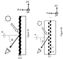
- the diffractive microstructures, or otherwise stated, the diffractive gratings are isotropic, parallel or crossed. They possess a period A and a depth t. The period A is in most cases smaller than the wavelength of light for which ZOF is designed.
- the waveguiding layer has a thickness c and is made of a material having an index of refraction n high that is higher than index of refraction (n low ) of the matter surrounding the waveguiding layer.
- the waveguiding layer is thus sometimes referred to as high-index waveguiding material or layer, and the matter surrounding the high-index waveguiding layer is sometimes referred to as low-index matter or layer.
- the low-index matter can have different indices of refraction.
- a first low-index matter can be a solid substrate, whilst a second low-index matter can be ambient air, as outlined herein below in greater detail with reference to Figure 2 .
- grating period A grating depth t
- grating profile or shape rectangular, sinusoidal (cf. Figure 1A ), triangular or more complex) and the indices of refraction n high and n low .
- the diffractive grating can be exposed to ambient air (cf. Figure 1B ).
- a ZOF 200 as known in the art comprises in the x/y-plane a waveguiding layer 220 having lower boundary 222 engaging with a substrate 210.
- Upper boundary 221 of waveguiding layer 220 is formed as a diffractive grating 225, which includes a plurality of protrusions 227 that are spaced apart from one another, and which is at the interface between waveguiding layer 220 and ambient air 230.
- the physical properties of diffractive grating 225 are at least defined by its physical dimensions, and more specifically, by its grating period A, the width p of protrusions 227 and thickness c of waveguiding layer 220.
- Waveguiding layer 220 has an index of refraction that is higher than that of air and that of substrate 210.
- ZOF 200 may enable the resonant coupling of light of several diffraction orders and thus of several wavelengths into waveguiding layer 220.
- the diffraction orders and the wavelengths that will be coupled into waveguiding layer 220 depend on at least one parameter of diffractive grating 225, the thickness c of the waveguiding layer 220 and differences in the index of refraction between waveguiding layer 220, substrate 210 and ambient air 230.
- the resonant coupling of incident light 250 into waveguiding layer 220 is schematically shown and exemplified as "+1" order light 253 and "-1" order light 254 having orders +1 and -1, respectively. Due to the higher index of refraction of waveguiding layer 220 compared to the one of ambient air 230 and substrate 210, "+1"- order light 253 and "-1"-order light 254 are totally internally reflected from upper boundary 221 and lower boundary 222 of waveguiding layer 220. However, a first portion of the zeroth-order (hereinafter: first zeroth-order light) 251 of incident light 250 is directly transmitted through waveguiding layer 220 and leaves ZOF 200 by propagation through substrate 210.
- first zeroth-order light hereinafter: first zeroth-order light
- second zeroth-order light 252 of light 250 is diffracted together with "-1" order light 254 into waveguiding layer 220. Both second zeroth-order light 252 and "-1"- order light 254 propagate in waveguiding layer 220 in opposite directions. After propagating over distance d in waveguiding layer 220, second zeroth-order light 252 is coupled out via diffractive grating 225.
- the resonance condition for the outcoupling of first zeroth-order light 251 and second zeroth-order light 252 can be tailored for a certain wavelength or wavelength range for the outcoupled light.
- the wavelength(s) of second zeroth-order light 252 outcoupled via diffraction grating 225 depends both on the viewing angle ⁇ out and the rotational orientation ⁇ of diffractive grating 225 with respect to a viewer 260. For each pair of angles ⁇ and ⁇ out a particular spectral range or color is reflected or transmitted.
- the spectral characteristics of such ZOFs are therefore tuneable.
- the reflection spectra R zero-order or transmission spectra T zero-order are the most prominent examples of the spectral characteristics of ZOFs.
- the transmission spectra are the complement of those in reflection.
- Security-related applications include the employment of ZOFs in anti-counterfeiting or forgery protection of, for example, documents (e.g., passports, visas, government forms); products (e.g., pharmaceuticals); and payment instruments (e.g., banknotes, credit cards, tickets and cheques); smart cards; and the like.
- Document US4484797 teaches a variable index-of-refraction optical medium of certain minimum thickness and periodicity with respect to the wavelength of incident light-if it meets certain specified constraints with respect to (1) relative indices-of-refraction of both its internal structure and that of its surroundings and (2) relative values of incident wavelength to periodicity and the relative indices-of-refraction-operates to produce both angularly-dependent subtractive-color filter reflection spectra and subtractive-color filter transmission spectra in accordance with its physical parameters.
- the methods for manufacturing the device taught in are based on vacuum deposition steps. Specifically, the medium is manufactured as laminated foil in roll-to-roll processes with thermally evaporated ZnS as the waveguiding layer deposited on foil substrates which were micro-structured by hot-embossing.
- Document WO2006038120 teaches a security device comprising first zero order diffractive microstructure on a substrate, a second zero order diffractive microstructure, and an intermediate light transmissive layer, separating the two diffractive microstructures.
- the spacing between the first and second diffractive microstructures is small enough so that optical interferences are produced between the diffractive microstructures.
- a further light transmissive layer covers the second diffractive microstructure.
- Document US2008024866 teaches ZOFs comprising a first layer having periodic diffractive microstructures and a second layer, wherein said first layer has a refractive index higher than said second layer by at least 0.2, and nanoparticles located in at least one of said layers which affect the refractive index of said at least one of said layers.
- the present invention further relates to methods of manufacturing such ZOFs, to the use such ZOFs e.g. in security devices and to the use of specific materials for manufacturing ZOFs.
- the manufacturing method disclosed is based on water based deposition of a porous layer on a foil substrate in a roll-to-roll process follower by a water based deposition of a polymeric waveguide layer and a subsequent microstructure embossing of the water soluble polymeric waveguide layer
- Document WO2004/077468 teaches a grid structure used for protecting valuable articles.
- the inventive structure consist of at least a first part provided with a grid constant which is less than a wavelength at which said part is observable and embodied in the form of a relief structure whose relief height is defined in such a way that the zero-order grid image can be observed in a determined spectral range.
- Said part has a size less than 0.5 mm at least in one direction.
- US2003017580 teaches a manufacturing method of a ZOF employable as a biosensor. Specifically, US2003017580 teaches a method for fabrication of a calorimetric resonant reflection biosensor structure comprising: (a) applying a liquid or semi-solid material that is capable of being transformed or cured into a flexible solid over a rigid master structure; (b) transforming the liquid or semi-solid material into a flexible master structure, wherein the flexible master structure has the rigid master structure embossed into a first surface of the flexible master structure; (c) peeling the flexible master structure from the rigid master structure; (d) placing the first surface of the flexible master structure onto a liquid or semi-solid layer, wherein the liquid or semi-solid layer is on a rigid substrate; (e) transforming or curing the liquid or semi-solid layer into a solid layer; (f) peeling the flexible master structure from the solid layer; and (g) applying a high refractive index dielectric film or reflective material over the solid layer, whereby a calorimetric
- Document US2007285782 teaches one or more zero-order diffractive pigments (ZOP) having both a particle distribution matrix material, and a layer of material in or on such a matrix material and having an index of refraction higher than that of the matrix material, and having a diffractive grating structure with a period in the range of 100 to 600 nm, which is smaller than the wavelength of light reflectable thereby in the zeroth reflection order.
- ZOPs the index of refraction of the matrix material is usually at least 0.25 less than that of the material of the layer, and the layer is typically of a thickness between 30 and 500 nm.
- Document EP 1862827 describes a nano-structured Zero-order diffractive filter comprising nanostructures on each grating element of the Zero-order diffractive filter and provides a uniform filter presenting bright colors to an observer.
- first low-index matter and “second low-index matter” may be interchangeably be used with term “first low-index layer” and “second low-index layer”, where the matter is a solid material.
- low-index and high-index are terms which are to be interpreted in relation to one another with reference to the same device.
- a low-index material or matter in a first device has a lower index of refraction than a high-index waveguide layer of the same first device.
- a first low-index matter of the first device may have a higher index of refraction than a first low-index matter of a second device.
- high-index material may be interchangeably be used with the term “waveguiding layer” or “high-index waveguiding layer”.
- lateral refers to any direction that is defined by the X and Y coordinates. Accordingly, the term “vertical” as used herein refers to Z-direction.
- determining may refer to methods whose output may be an estimate of a parameter.
- the present invention discloses a security related zero-order diffractive filter for preventing counterfeiting comprising:a high-index material having an upper surface and a lower surface;wherein said high-index material is positioned between a first low-index matter and a second low-index matter ;wherein said lower surface is adjacent to said first low-index matter and wherein said upper surface is adjacent to said second low-index matter;wherein a diffractive grating structure is provided on the first low-index matter; wherein said high-index materialhas an index of refraction that is higher than the index of refraction of both said first low-index matterand said second low-index matter;said high-index material being laterally patterned on said first low-index matter, such that said zero-order diffractive filter forms high-index islands and areas free of high-index material between said high-index islands; characterized in thatsaid high-index islands have a size at least four times the grating period of said lower diffractive grating structure in any lateral direction so that they are resolvable by
- the at least one area the index of refraction of the first low-index matter is at least approximately equal to the index of refraction of the second low-index matter.
- the area free of high index material is substantially free of diffraction.
- the high-index material between the first and the second low-index matter has predetermined vertical dimensions.
- the high-index material has an index of refraction n that is higher than 1.8, higher than 1.9, or higher than 2.
- the high-index material comprises nano-structured material.
- the high-index material comprises organic material.
- the laterally patterned high-index material is patterned in the shape of a logo or text or numbers or barcodes.
- ZOFs By employing wet-coating techniques according to embodiments of the invention for the manufacturing of ZOFs, the latter remains non-subjected to the phenomenon of swelling and/or dissolution. Furthermore, ZOFs that include water soluble layers cause problems in applications where products comprising such ZOFs have to withstand various tests such, for example, washing machine test for banknotes.
- the difference between the index of refraction n high of the high-index material and the index of refraction n low of the surrounding low-index matter may be, for example, at least 0.1, 0.15, and 0.2
- n low may for example have values ranging from 1.1 to 1.7; and n high may be, for example, at least 1.8, at least 1.9, or at least 2.0.
- parameters for the diffractive grating and the high-index waveguiding material may be as outlined herein below in Table 1:
- the method for manufacturing a ZOF includes the procedure of determining the compatibility between two layers of material according to at least one compatibility criterion, which will be outlined in greater detail herein below. If it is determined that the two layers are sufficiently compatible, then wet-coating techniques according to embodiments of the invention are employed for the manufacturing of a zero-order diffraction filter, which includes the two layers adjacent to one another. Sufficient compatibility between the solvent of overprinting material and a micro-structured and wet-coated layer is of high importance because in case of insufficient compatibility, the solvent of the overprinting may destroy the microstructure forming the diffractive grating due to, e.g., swelling and/or dissolution of the microstructure.
- solvents dissolves and/or swells a layer containing organic material depends on the solubility of the organic material in this solvent. Many different types and possible classification for solvents exist. Solvents may for example be classified according to their polarity index, a relative measure indicating the degree of interaction of the solvent with various polar test solutes.
- Table 2 below exemplifies several solvents and with their corresponding polarity index. Most of the data listed in the following tables are taken from " CRC handbook of solubility parameters and other cohesion parameters", Allan F. M. Barton, Edition: 2, CRC Press, 1991, p.292 and p.406, ISBN 0849301769 . In Table 2 below, the solvents are listed in order of increasing polarity index.
- each layer including organic material (e.g., polymers) dissolved in solvents shall be deposited on top of each other.
- the at least one compatibility criterion may for example refer to a minimal difference in the polarity index between the two layers.
- the difference in the polarity indices between the two layers may be for example at least 0.25, 0.5, or 1.
- ⁇ G m ⁇ H m ⁇ T ⁇ ⁇ S m
- ⁇ H m V m ⁇ ⁇ H V 1 / V 1 0.5 ⁇ ⁇ H V 2 / V 2 0.5 2 ⁇ ⁇ 1 ⁇ ⁇ 2
- V m represents the total volume of the blended mixture, ⁇ H V1 and ⁇ H V2 the molar vaporization heat or latent heat; V 1 and V 2 the molar volumes; and ⁇ 1 and ⁇ 2 the volume fractions of component 1 and 2, respectively.
- the ratio ⁇ H V / V is referred to as the cohesive energy density, which is defined as the amount of energy needed to completely remove a unit volume of molecules from their neighbors to infinite separation, assuming an ideal gas.
- the cohesive energy density is equal to the heat of vaporization divided by molar volume. In order for a material to dissolve, the attracting interactions need to be overcome such that molecules surrounded by a solvent are separated from each other and therefore dissolved.
- the Hildebrand solubility parameter provides a quantitative estimate of the degree of interaction between materials, and is used according to an embodiment of the invention as an indicator with regards to solubility of a first matter in second matter, and particularly for the solubility of non-polar materials like, for example, at least some polymers.
- the Hildebrand solubility parameter enables to predict the interaction between two matters of non-polar and slightly polar systems that are free of hydrogen bonding.
- the Hildebrand solubility parameter may, for example, be applied for predicting interaction, or more specifically, for example, the solubility and/or swelling between of a polymer by a solvent.
- solubility-reducing procedures may be performed on matter to at least reduce solubility or to render the matter insoluble a solvent.
- Such solubility-reducing procedures may include, for example, performing cross-linking on matter containing organic material.
- Cross-linking may, include, for example, ultraviolet cross-linking of, e.g., a polymer layer.
- solubility-reducing procedures like, e.g. heat treatments or pressure, may be employed in cases where cross-linking may be not suffice to prevent swelling and the resulting destructing of diffractive microstructures.
- Table 2 exemplifies some values of ⁇ for solvents, Table 3 for polymers and Table 4 for plasticizers. It should be noted that the solvents, polymers and plasticizers exemplified herein are by no means to be construed as limiting.
- the at least one compatibility criterion relates to the interaction parameter from the Flory-Huggins theory.
- the interaction parameter is both temperature and molecular weight dependent but concentration independent.
- the entropic contribution is very small and the miscibility or immiscibility of the system mainly depends on the value of the enthalpy of mixing.
- a negative value for the interaction parameter indicates miscibility.
- miscibility may be existent, for example, for values that are below 0.01, e.g., for some polymers used in printing applications in a solvent.
- increased values equal above 0.01 for the interaction parameter indicate increased compatibility.
- the method for manufacturing a ZOF may include the procedure of determining the interaction parameter of a first polymer in a solvent. If the interaction parameter of the first polymer with the solvent meets the at least one compatibility criterion, i.e., the interaction parameter is sufficiently high, the method may further include the procedure of depositing the first polymer as a first layer, and the deposition of a second polymer as a second layer on top of the first layer by employing the respective solvent.
- the interaction parameter between the first polymer and the solvent may be, for example, at least 0.01, at least 0.05, at least 0.25, or at least 0.5, if the first layer should not be dissolved and/or swelled upon the deposition of the second layer due the employment of the solvent.
- solubility parameters such as, for example, 3-Dimensional Solubility Parameters like, e.g., Hansen Solubility Parameters, may be employed for determining the solubility of polar molecules.
- the manufacturing of a Zero-Order Diffractive includes the employment of at least one wet-coating technique. In some embodiments, solely wet-coating techniques may be employed.
- a wet-coating technique for the deposition of layers is employed if it is determined that the above-mentioned at least one compatibility criterion is met.
- a wet-coating technique that may be employed for the manufacturing of a ZOF may include, for example, at least one of the following processes: spreading; brushing; coating; pouring; spraying; printing; roller coating methods; and any other wet-coating manufacturing process, e.g., as known in the art.
- Printing processes may for include, for example, at least one of the following: screen printing; flexography; digital printing methods; gravure printing, ink-jet printing; and any other printing method, e.g., as known in the art.
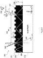
- a ZOF 301 includes a substrate 305; a layer of embossable first low-index matter 310 having an upper surface 312; a layer of high-index (waveguiding) material 320; and second low-index matter 330.
- First low-index matter 310 is deposited on substrate 305 such to cover substrate 305 at least partially.
- first low-index matter 310 may be positioned between substrate 305, and below either one high-index material 320 (sandwich area) and second low-index matter 330 (merged area), depending on the lateral position in a ZOF according to an embodiment like, e.g., ZOF 301.
- first low-index matter 310 and second low-index matter 330 engage with one another, whereas in sandwich positions 341 and 343, high-index material 320 is positioned between first low-index matter 310 and second low-index matter 330.
- a second low-index matter of a ZOF according to an embodiment of the invention may be, for example, ambient air.
- first low-index matter 310 may cover substrate 305 completely. In another embodiment of the invention, first low-index matter 310 may cover substrate 305 only partially (not shown). For example, first low-index matter 310 may be laterally patterned in a manner forming, e.g., individual islands of first low-index matter 310 (not shown) and/or a grid-like patterns (not shown) of first low-index matter 310, on substrate 305. According to an embodiment of the invention, embossible first low-index matter 310 may have thickness ranging, for example, from 200 nm to 10 ⁇ m.
- the thickness of a first low-index matter deposited on a substrate may vary for different lateral positions on the substrate (not shown).
- a first island of the first low-index matter may be of first height h 1 (e.g., 200 nm), whilst a second island of the first low-index matter deposited on the substrate may have a different height h 2 (e.g. 500 nm).
- h 1 e.g. 200 nm
- h 2 e.g. 500 nm
- a ZOF may feature additional or alternative vertical distributions of the first low-index matter on substrate.
- upper surface 312 of first low-index matter 310 is at least partially formed as a lower diffractive grating structure 315.
- Lower diffractive grating structure 315 exemplified in Figure 3A extends entirely over upper surface 312, i.e., diffractive grating constitutes upper surface 312.
- a grating structure may extend only some part(s) of upper surface, for example, in a laterally patterned manner.
- the position of individual grating structures may be at least approximately aligned with the position of laterally patterned low-index matter and optionally have the at least approximately the same lateral dimensions as the laterally patterned low-index matter.
- lower diffractive grating structure 315 is provided on first low-index matter 310 by employing, for example, hot-embossing and/or UV-embossing, in e.g., roll and/or batch processes.
- a ZOF may be free of a substrate. Accordingly, in a ZOF according to an embodiment of the invention, first low-index matter 310 may constitute a substrate which may be made of, for example, PMMA or PC foils.
- the parameters (e.g., height, period, form and grating orientation, index of refraction) of a diffractive grating like, e.g., lower diffractive grating structure 315 may be uniform in ZOF 301.
- at least one parameter of lower diffractive grating structure 315 may be non-uniform in ZOF 301.
- the orientation of lower diffractive grating structure 315 may be different or vary with respect to the lateral its position in ZOF 301.
- embossing shims may be provided for micro-structuring a diffractive grating structure like, e.g., lower diffractive grating structure 315.
- a diffractive grating structure like, e.g., lower diffractive grating structure 315.
- such shims may be provided in step and repeat process with micro-structured areas in the shape of logos for example.
- the lateral size of logos implemented by ZOFs may be in the millimeter in order to be resolvable by the human eye.
- the logos may also be of smaller size, for example, in machine-reading authenticating applications, or in combined human-eye and machine-reading applications.
- high-index material 320 is provided on first low-index matter 310 by employing a wet-coating technique.
- the high-index material covers the first low-index layer only partially, e.g., according to a predetermined lateral pattern or structure.
- high-index material may be patterned to form a plurality of individual islands or spots.
- Each high-index island or spot may have a predetermined structure and position with respect to neighboring high-index islands, as schematically illustrated and exemplified in Figure 3B , with respect to high-index material 320, which is laterally patterned to high-Index islands 320A and 320B.
- the lateral pattern of high-index material schematically illustrated in Figure 3A should not be construed as limiting.
- the high-index material of a ZOF may for example include more than two high-index islands that are laterally patterned such to form, for example, (with respect to the top view onto x-y plane), a plurality of at least approximately parallel stripes which may constitute, for example, a barcode.
- the plurality of high-index islands may have at least one the following predetermined shapes: an arbitrary shape; and an at least approximately circular; oval, polygonal shape; a shape representing a graphic symbol (e.g., a number, a letter, a logo).
- the high-index material may be laterally patterned such to form a macroscopic grid-like structure.
- high-index material 320 may be provided in a laterally patterned manner onto first low-index matter such that a plurality of high-index islands (e.g., high-index islands 320A and 320B ) form logos, images, barcodes, and the like. Only those parts of ZOF 301 covered by high-index material 320 show the zero-order diffraction color effect.
- each high-index island like, e.g., high-index islands 320A and 320B is at least four times the grating period of lower diffractive grating structure 315 in any lateral direction.
- the size between the outer boundaries of such high-index islands may range, for example, between 10 ⁇ m and 100 mm, between 20 ⁇ m and 20 mm, between 50 ⁇ m and 5 mm; or between 100 ⁇ m and 1 mm.
- a second low-index matter may be provided, which may constitute a cover and/or a protective layer of the corresponding ZOF, and specifically, of the high-index material. Accordingly, the high-index material or waveguiding layer is embedded in a ZOF according to an embodiment of the invention, and may thus be protected from touch and/or environmental influences.
- a ZOF 302 and a ZOF 303 may include second low-index matter 330.
- low-index matter 330 engages with both the upper surfaces of both the high-index material 320 and first low-index matter 310.
- high-index islands 320A and 320B are embedded from above and their sides by second low-index matter 330, and from below from first low-index matter 310.
- a high-index material 320 may in some embodiments of the invention be vertically structured, i.e., height of high-index material 320 may vary as a function of its lateral position.
- Such a high-index material and is thus with respect Figure 3C referred to as a height-patterned structure 321.
- Height-patterned structure 321 may be at least partially embedded between first low-index matter 310 and second low-index matter 331.
- Wet-coating techniques that may be employed for such vertical structuring may include, for example, gravure printing by varying the parameter of the gravure cylinder such as the depth of the cups.
- Such ZOFs show multi-color effects as different waveguiding layer thicknesses result in different resonance conditions for the ZOF.
- the crossover between parts of different layer thicknesses can be in step form (as schematically shown in Figure 3C ) or as a gradient.
- Combining the laterally and optionally vertically patterned waveguiding layer and the laterally patterned microstructures i.e., lower diffractive grating structure 315 ) results in a complex color effect which is extremely difficult to counterfeit.
- the indices of refraction of first and the second low-index matter of a ZOF according to an embodiment of the invention may be at least approximately equal.
- first or higher order diffraction effects disappear in the lateral positions that are free of any interlaying high-index material 320, i.e., in merged areas 342.
- Such merged-areas 342 are areas free of high-index material substantially free of diffraction-effects on light.
- the method for manufacturing a ZOF like, e.g., ZOF 401 includes the procedure of providing first low-index matter 410, which may optionally be provided on a substrate 405.
- first low-index matter 410 constitutes a substrate.
- Providing first low-index matter 410 is accomplished by employing a wet-coating process, e.g., as known in the art. Analogous to what is described above with reference to Figure 3A , first low-index matter 410 covers at least partially substrate 405. The low-index matter may cover the substrate entirely. Alternatively, first low-index matter 410 may cover substrate 405 only partially and may be, for example, laterally patterned (not shown).
- First low-index matter may have a thickness ranging, for example, between 200 nm and 10 ⁇ m.
- upper surface 412 is at least approximately flat. However, this should by no means to be construed as limiting. Accordingly, in an embodiment of the invention, upper surface 412 of the low-index matter may be at least partially microstructured (not shown).
- the method for manufacturing includes the procedure of providing high-index material 420 having an upper surface 412 onto first low-index matter 410 such to partially cover the latter according to a predetermined pattern, by employing a wet-coating technique.
- high-index material 420 may cover first low-index matter 410 partially, for example, in a laterally patterned manner forming high-index islands 421.
- high-index material 420 is provided onto first low-index matter 410 such to form on the latter logos, images, barcodes, and the like. Only those parts of the device which are covered by high-index material 420 show zero-order diffraction color effect in a ZOF according to an embodiment of the invention like, e.g., ZOFs 401, 402 and 403.
- An upper diffractive grating structure 415 is provided on upper surface 412 employing, for example, hot- or UV-embossing.
- embossable high-index materials 420 include, but are not limited to, blends of polyvinyl alcohol (PVA) comprising TiO 2 nano-particles; or gelatin comprising PbS..
- nanoparticles that may be present in high-index matter remain separated from one another. Otherwise stated, the agglomeration of the nanoparticles is prevented.
- the minimal size of each individual high-index island 421 is, for example, at least four times the grating period of diffractive grating structure 415 in any lateral direction the size of such high-index islands is in the range of 10 ⁇ m up to 100 mm, preferably between 20 ⁇ m and 20mm, especially preferred in the range of 50 ⁇ m and 5 mm and particularly preferred between 50 ⁇ m and 1 mm.
- a second low-index matter may be provided.
- the second low-index matter is provided onto the high-index material only.
- second low-index matter 430 is provided on both first low-index matter 410 and high-index material 420.
- second low-index matter 430 is provided directly onto first low-index matter 410 where no interlaying high-index islands like, e.g., high-index islands 420A and 420B, are present.
- providing second low-index matter 430 renders high-index material embedded in ZOF 402 and 403, respectively. Accordingly, high-index material may be protected from touch or environmental influences.
- a ZOF may include an adhesive layer (not shown) that is adhesive with other substrates such as, for example, e.g. Banknotes, Passports, and the like.
- the method may therefore include according to some embodiments of the invention the procedure of providing the adhesive layer onto second low-index matter 430; if present, onto substrate 405; or onto first low-index matter 410.
- Providing the adhesive layer onto substrate 405 or first low-index matter 410 may require flipping of a ZOF like, e.g., ZOF 402 or 403.
- the adhesive layer may be, for example, a thermo-activatable adhesive layer.
- a ZOF according to an embodiment of the invention like, e.g., ZOF 403, includes high-index material 420 that may be vertically structured. Otherwise stated, height of high-index matter may be non-uniform (analogous to what is described with respect to high-index material 320 in Figure 3C ). Such vertically structured high-index material 420 is hereinafter referred to as height-patterned structure 421.
- the vertical structuring may be accomplished in one step.
- Wet-coating techniques that may be employed for such vertical structuring may include, for example, gravure printing by varying the parameter of the gravure cylinder such as the depth of the cups.
- Such devices will show multi-color effects as different waveguiding layer thicknesses result in different resonance conditions for the ZOF.
- the crossover between parts of different layer thicknesses can be in step form (as schematically shown and exemplified in Figure 4C ) or as a gradient.
- the high-index material is applied by employing a method which permits the application of highly homogeneous layer thicknesses over large areas. Homogeneity of the layer thickness of the high-index material is required in order to ensure a uniform color appearance in the finished ZOF.
- a wet-coating technique includes the employment of a printing method in which the coloring substance or the lacquer is applied from a temperature-regulated coating pan with a dipping roller and a transfer cylinder onto the printing cylinder, wherein substantially only the depressions of the printing cylinder are filled with the coloring or the coating substance. Excess coloring or coating substance may be removed by an excess remover such as, for example, a blade and optionally by a blowing strip.
- Substrates 305 and 405 may be made, for example, of silicon wafers, glass, quartz, paper, polymer foils, and or any other suitable material. Specifically, the materials may be flexible films of synthetic materials like, for example, of PI, PP, MOPP, PE, PPS, PEEK, PEK, PEI, PSU, PAEK, LCP, PEN, PBT, PET, PA, PC, COC, POM, ABS, PVC. Substrates 305 and 405 may have a thickness ranging for example, from 5 ⁇ m to 700 ⁇ m, from 8 ⁇ m to 200 ⁇ m, or from 12 ⁇ m to 50 ⁇ m.
- metal foils like, for example Al, Cu, Sn, Ni, Fe or special steel foils having a thickness ranging for example, from 5 ⁇ m to 200 ⁇ m, from 10 ⁇ m to 80 ⁇ m, or from 20 ⁇ m to 50 ⁇ m may be employed for substrates 305 and 405.
- Such foils may in some embodiments be surface-treated, like, e.g., coated and/or laminated, for example with adhesion promoting materials and/or they can be lacquered.
- Alternative materials that may be employable for implementing substrates 305 and 405 may include, for example, cellulose-free or cellulose-containing paper, thermally activatable paper or composites with paper, for example composites with synthetic materials having a weight per unit area of 20-500 g/m 2 or 40-200 g/m 2 .
- substrate 305 and 405 may be coated with a release layer to enable the transfer of the deposited layer setup on other substrates, e.g. banknotes or passports.
- embossable materials suitable for the implementation of first low-index matter 310 and 410 include, for example, synthetic organic materials such as thermoplastic acrylic lacquer or UV-curable organic materials, particularly polymer. Concrete examples are ethylene vinyl acetate, polyvinyl acetate, polystyrene, polyurethane and combinations thereof. If first low-index matter 310 and 410 possesses an at least approximately flat surface, they may also be made of, for example, color or lacquer systems based on nitrocellulose, epoxy, polyester, colophonium, acrylate, alkyd, melamine, PVA, PVAc, PVC, isocyanate or urethane systems.
- waveguiding high-index material or layer 320 and 420 is made of organic material.
- examples include high-index refraction polymers.
- high-index material 320 and 420 may be made of by hybrid materials comprising inorganic nano-particle or flakes embedded in an organic matrix.
- the refractive index of the nano-particle or flakes is higher than the one of the organic matrix.
- examples of such inorganic nanoparticles include PbS, TiO 2 , SiO 2 , Al 2 O 3 and ZrO 2 .
- the organic matrix can be e.g.
- the size of the nano-particles or flakes is at least in one special direction in the range of, e.g., 5 nm to 200 nm or, for example, between 10 nm and 60 nm. Furthermore, the particle size distribution may be preferably low.
- Still another possible material for the waveguiding layer is titanium dioxide (TiO 2 ) paste, e.g. HTL/SC from Solaronix SA. This paste consists of TiO 2 nanoparticles have a size of about 9 nm and thus perfectly fit into the grooves of the grating. The solid content of this paste is at least approximately 3%. A heat treatment (e.g. 2 minutes at 130°C) of the printed material is done in order to sinter the nanoparticles into a solid TiO 2 film.
- a special type of hybrid materials that can be used as waveguiding second layer is organometallic polymer.
- organometallic polymer When cured at elevated temperatures, the organometallic polymer decomposes to form a highly dispersed metal oxide phase that imparts high index properties to the final hybrid coating.
- Such hybrid materials are described in "High-refractive-index polymer coatings for optoelectronics applications" in Advances in Optical Thin Films. Edited by Amra, Claude; Kaiser, Norbert; Macleod, H. Angus. Proceedings of the SPIE, Volume 5250, pp. 423-434 (2004), http://dx.doi.ora/10.1117/12.513363 .
- high index of refraction polymers that may be employed for implementing high-index material 320 and 420 are for example the OptiNDEX series (Brewer Science Inc., USA) as disclosed in "Thin-film polyetherimides with controlled refractive indices" in Organic Photonic Materials and Devices VI. Edited by Grote, James G.; Kaino, Toshikuni. Proceedings of the SPIE, Volume 5351, pp. 276-283 (2004), http://dx.doi.ora/10.1117/12.529576 .
- An alternative are the polymers of the C-imide series (Optmate Corporation, Japan with n high up to 1.78 at a wavelength of 589 nm.
- first low-index matter 410 is provided by employing, e.g., gravure printing.
- First low-index matter 410 may have a thickness of, e.g., 2 ⁇ m and may be made of e.g., Nitrocellulose (E330 of Dow Chemical Company).
- High-index material 420 may be provided by deposition on top of first low-index matter using, for example, gravure printing.
- the layer thickness of high-index material 420 may, for example, be about 300 nm.
- the layer of first low-index matter implemented with NC may thus have an index of refraction of, e.g., at least approximately 1.54 for a wavelength of 510 nm.
- the layer of high-index material 420 implemented in an embodiment with polyimide may have an index of refraction of at least approximately 1.72.
- the manufacturing of a ZOF may be performed with shadow-mask-free procedures.
- the output rate of ZOFs manufactured according to embodiments of the invention may be, for example 100 m 2 /min in, e.g., roll-to-roll processes.
Claims (6)
- Sicherheitsrelevantes Beugungsfilter nullter Ordnung zum Verhindern von Fälschungen, Folgendes umfassend:ein Hochindexmaterial (320, 420) mit einer Oberseite und einer Unterseite,wobei das Hochindexmaterial (320, 420) zwischen einem ersten Niedrigindex-Gegenstand (310, 410) und einem zweiten Niedrigindex-Gegenstand (330, 430) positioniert ist,wobei die Unterseite an den ersten Niedrigindex-Gegenstand (310, 410) grenzt und die Oberseite an den zweiten Niedrigindex-Gegenstand (330, 430) grenzt,wobei am ersten Niedrigindex-Gegenstand (310, 410) eine Struktur eines Beugungsgitters (315, 415) bereitgestellt ist,wobei das Hochindexmaterial (320, 420) einen Brechungsindex aufweist, der höher als der Brechungsindex von sowohl dem ersten Niedrigindex-Gegenstand (310, 410) als auch dem zweiten Niedrigindex-Gegenstand (330, 430) ist,wobei das Hochindexmaterial (320, 420) auf dem ersten Niedrigindex-Gegenstand (310, 410) derart seitlich strukturiert ist, dass der Beugungsfilter nullter Ordnung Hochindexinseln (320A, 320B, 420A, 420B, 321, 421) und zwischen den Hochindexinseln Bereiche (342), die frei von Hochindexmaterial sind, bildet,dadurch gekennzeichnet, dass die Hochindexinseln (320A, 320B, 420A, 420B, 321, 421) eine Größe aufweisen, die in jeder seitlichen Richtung mindestens das Vierfache der Gitterperiode der Niedrigbeugungs-Gitterstruktur (315) beträgt, so dass sie vom menschlichen Auge und/oder von Anwendungen zur Authentifizierung durch Maschinenlesen zerlegbar sind.
- Beugungsfilter nullter Ordnung nach Anspruch 1, dadurch gekennzeichnet, dass in dem mindestens einen Bereich der Brechungsindex des ersten Niedrigindex-Gegenstandes dem Brechungsindex des zweiten Niedrigindex-Gegenstandes mindestens ungefähr gleicht.
- Beugungsfilter nullter Ordnung nach Anspruch 1 oder 2, dadurch gekennzeichnet, dass der Bereich, der frei von Hochindexmaterial ist, im Wesentlichen frei von Beugungseffekten von Licht ist.
- Beugungsfilter nullter Ordnung nach einem der Ansprüche 1 bis 3, dadurch gekennzeichnet, dass das Hochindexmaterial zwischen dem ersten und dem zweiten Niedrigindex-Gegenstand festgelegte vertikale Abmessungen aufweist.
- Beugungsfilter nullter Ordnung nach einem der Ansprüche 1 bis 4, dadurch gekennzeichnet, dass das Hochindexmaterial einen Brechungsindex n aufweist, der höher als 1,8 ist.
- Beugungsfilter nullter Ordnung nach einem der Ansprüche 1 bis 5, dadurch gekennzeichnet, dass das Hochindexmaterial ein nanostrukturiertes Material aufweist.
Applications Claiming Priority (1)
| Application Number | Priority Date | Filing Date | Title |
|---|---|---|---|
| US21350309P | 2009-06-15 | 2009-06-15 |
Publications (2)
| Publication Number | Publication Date |
|---|---|
| EP2264491A1 EP2264491A1 (de) | 2010-12-22 |
| EP2264491B1 true EP2264491B1 (de) | 2017-08-09 |
Family
ID=42470538
Family Applications (1)
| Application Number | Title | Priority Date | Filing Date |
|---|---|---|---|
| EP10165817.7A Revoked EP2264491B1 (de) | 2009-06-15 | 2010-06-14 | Diffraktionsfilter nullter Ordnung und Herstellungsverfahren dafür |
Country Status (3)
| Country | Link |
|---|---|
| US (1) | US8970955B2 (de) |
| EP (1) | EP2264491B1 (de) |
| AU (1) | AU2010202486B2 (de) |
Families Citing this family (12)
| Publication number | Priority date | Publication date | Assignee | Title |
|---|---|---|---|---|
| EP2447744B1 (de) * | 2010-11-01 | 2021-03-31 | CSEM Centre Suisse d'Electronique et de Microtechnique SA - Recherche et Développement | Pixelierter optischer filter und verfahren zu dessen herstellung |
| EP2447743B1 (de) * | 2010-11-01 | 2016-10-26 | CSEM Centre Suisse d'Electronique et de Microtechnique SA - Recherche et Développement | Isotropes optisches Filter und Herstellungsverfahren dafür |
| DE102012105571B4 (de) * | 2012-06-26 | 2017-03-09 | Ovd Kinegram Ag | Dekorelement sowie Sicherheitsdokument mit einem Dekorelement |
| DE102012108169A1 (de) | 2012-09-03 | 2014-05-28 | Ovd Kinegram Ag | Sicherheitselement sowie Sicherheitsdokument |
| JP6264950B2 (ja) * | 2013-05-22 | 2018-01-24 | パナソニックIpマネジメント株式会社 | 有機el照明の光取り出し基板 |
| DE102015100520A1 (de) | 2015-01-14 | 2016-07-28 | Leonhard Kurz Stiftung & Co. Kg | Mehrschichtkörper und Verfahren zu dessen Herstellung |
| US9846276B2 (en) * | 2015-04-14 | 2017-12-19 | Washington State University | Low-cost fiber optic sensor for large strains |
| EP3443598B1 (de) | 2016-04-15 | 2019-08-14 | Lumileds Holding B.V. | Breitbandspiegel, leuchtdiode mit einem breitbandspiegel, und verfahren zur herstellung eines breitbandspiegel |
| JP7003928B2 (ja) * | 2016-10-21 | 2022-01-21 | 大日本印刷株式会社 | 積層体、冊子体 |
| JP6977255B2 (ja) * | 2016-12-09 | 2021-12-08 | 大日本印刷株式会社 | 導光フィルム、偽造防止用構造体および偽造防止物品 |
| FR3087385B1 (fr) | 2018-10-19 | 2021-03-12 | Surys | Film de securite et document securise au moyen d'un film de securite |
| FR3111843A1 (fr) | 2020-06-30 | 2021-12-31 | Surys | Procédés de fabrication de composants optiques de sécurité, composants optiques de sécurité et objets sécurisés équipés de tels composants |
Citations (1)
| Publication number | Priority date | Publication date | Assignee | Title |
|---|---|---|---|---|
| WO2009068462A1 (en) * | 2007-11-27 | 2009-06-04 | Basf Se | Use of zero-order diffractive pigments |
Family Cites Families (15)
| Publication number | Priority date | Publication date | Assignee | Title |
|---|---|---|---|---|
| US4484797A (en) | 1981-07-20 | 1984-11-27 | Rca Corporation | Diffractive subtractive color filter responsive to angle of incidence of polychromatic illuminating light |
| US7667895B2 (en) * | 1999-07-08 | 2010-02-23 | Jds Uniphase Corporation | Patterned structures with optically variable effects |
| GB0015873D0 (en) * | 2000-06-28 | 2000-08-23 | Rue De Int Ltd | Optically variable security device |
| DE10036505A1 (de) * | 2000-07-27 | 2003-08-14 | Orga Kartensysteme Gmbh | Optisch wirksame Struktur zur Personalisierung von Karten u. dgl., sowie Verfahren zu deren Herstellung |
| US7101660B2 (en) | 2000-10-30 | 2006-09-05 | Sru Biosystems, Inc. | Method for producing a colorimetric resonant reflection biosensor on rigid surfaces |
| DE10308327A1 (de) | 2003-02-26 | 2004-09-09 | Giesecke & Devrient Gmbh | Sicherheitselement |
| GB0401060D0 (en) * | 2004-01-19 | 2004-02-18 | Ezra David | Optical devices |
| GB0422266D0 (en) | 2004-10-07 | 2004-11-10 | Suisse Electronique Microtech | Security device |
| GB0504959D0 (en) * | 2005-03-10 | 2005-04-20 | Rue International De La Ltd | Security device based on customised microprism film |
| US7481256B2 (en) * | 2005-07-25 | 2009-01-27 | Sayers Charles P | protective device for rotary lawn mower blade |
| US7864424B2 (en) | 2006-05-31 | 2011-01-04 | CSEM Centre Suisse d'Electronique et de Microtechnique SA-Recherche et Développement | Zero order pigments (ZOP) |
| EP1862827B2 (de) * | 2006-05-31 | 2012-05-30 | CSEM Centre Suisse d'Electronique et de Microtechnique SA - Recherche et Développement | Nanostrukturierter Diffraktionsfilter nullter Ordnung |
| US7821691B2 (en) * | 2006-07-28 | 2010-10-26 | CSEM Centre Suisse d'Electronique et de Microtechnique SA—Recherche et Développement | Zero-order diffractive filter |
| US20080024866A1 (en) | 2006-07-28 | 2008-01-31 | Harald Walter | Zero-order diffractive filter |
| US8542442B2 (en) * | 2007-05-07 | 2013-09-24 | Centre Suisse d'Electronique et de Microtechnique SA—Recherche et Developpement | Isotropic zero-order diffractive filter |
-
2010
- 2010-06-14 EP EP10165817.7A patent/EP2264491B1/de not_active Revoked
- 2010-06-15 AU AU2010202486A patent/AU2010202486B2/en active Active
- 2010-06-15 US US12/815,726 patent/US8970955B2/en active Active
Patent Citations (1)
| Publication number | Priority date | Publication date | Assignee | Title |
|---|---|---|---|---|
| WO2009068462A1 (en) * | 2007-11-27 | 2009-06-04 | Basf Se | Use of zero-order diffractive pigments |
Also Published As
| Publication number | Publication date |
|---|---|
| US20100315713A1 (en) | 2010-12-16 |
| EP2264491A1 (de) | 2010-12-22 |
| AU2010202486A1 (en) | 2011-01-06 |
| AU2010202486B2 (en) | 2015-06-11 |
| US8970955B2 (en) | 2015-03-03 |
Similar Documents
| Publication | Publication Date | Title |
|---|---|---|
| EP2264491B1 (de) | Diffraktionsfilter nullter Ordnung und Herstellungsverfahren dafür | |
| EP2021837B1 (de) | Optisch reflektierende oberflächen-reliefmikrostrukturen und herstellungsverfahren dafür | |
| US9618839B2 (en) | Surface relief microstructures, related devices and method of making them | |
| EP1862827B2 (de) | Nanostrukturierter Diffraktionsfilter nullter Ordnung | |
| US7821691B2 (en) | Zero-order diffractive filter | |
| EP2024447B1 (de) | Bindemittel mit Pigmenten mit Farbeffekten auf Basis einer Beugung nullter Ordnung | |
| EP1775142B1 (de) | Ein diffraktives Sicherheitselement | |
| US8133638B2 (en) | All-polymer grating microstructure | |
| EP1990661B1 (de) | Isotroper Diffraktionsfilter nullter Ordnung | |
| RU2587072C1 (ru) | Неизометрический отражательный отображающий элемент, носитель информации, использующий неизометрический отражательный отображающий элемент | |
| US20080088895A1 (en) | Article With Micro Indicia Security Enhancement | |
| FR3020986A1 (fr) | Dispositif de securite hybride pour document de securite ou jeton | |
| WO2011116419A1 (en) | High refractive index coatings and their use in the protection of surface relief structures | |
| CN107615111B (zh) | 层叠体及其制造方法 | |
| WO2017025336A1 (en) | Azimuthally modulated scattering device |
Legal Events
| Date | Code | Title | Description |
|---|---|---|---|
| PUAI | Public reference made under article 153(3) epc to a published international application that has entered the european phase |
Free format text: ORIGINAL CODE: 0009012 |
|
| AK | Designated contracting states |
Kind code of ref document: A1 Designated state(s): AL AT BE BG CH CY CZ DE DK EE ES FI FR GB GR HR HU IE IS IT LI LT LU LV MC MK MT NL NO PL PT RO SE SI SK SM TR |
|
| AX | Request for extension of the european patent |
Extension state: BA ME RS |
|
| 17P | Request for examination filed |
Effective date: 20110615 |
|
| 17Q | First examination report despatched |
Effective date: 20111213 |
|
| GRAP | Despatch of communication of intention to grant a patent |
Free format text: ORIGINAL CODE: EPIDOSNIGR1 |
|
| STAA | Information on the status of an ep patent application or granted ep patent |
Free format text: STATUS: GRANT OF PATENT IS INTENDED |
|
| RIC1 | Information provided on ipc code assigned before grant |
Ipc: G02B 27/44 20060101ALI20170217BHEP Ipc: G02B 5/18 20060101AFI20170217BHEP Ipc: B42D 15/00 20060101ALI20170217BHEP Ipc: G07D 7/00 20160101ALI20170217BHEP |
|
| INTG | Intention to grant announced |
Effective date: 20170314 |
|
| GRAS | Grant fee paid |
Free format text: ORIGINAL CODE: EPIDOSNIGR3 |
|
| GRAA | (expected) grant |
Free format text: ORIGINAL CODE: 0009210 |
|
| STAA | Information on the status of an ep patent application or granted ep patent |
Free format text: STATUS: THE PATENT HAS BEEN GRANTED |
|
| AK | Designated contracting states |
Kind code of ref document: B1 Designated state(s): AL AT BE BG CH CY CZ DE DK EE ES FI FR GB GR HR HU IE IS IT LI LT LU LV MC MK MT NL NO PL PT RO SE SI SK SM TR |
|
| REG | Reference to a national code |
Ref country code: GB Ref legal event code: FG4D |
|
| REG | Reference to a national code |
Ref country code: CH Ref legal event code: EP Ref country code: AT Ref legal event code: REF Ref document number: 917453 Country of ref document: AT Kind code of ref document: T Effective date: 20170815 |
|
| REG | Reference to a national code |
Ref country code: CH Ref legal event code: NV Representative=s name: NOVAGRAAF INTERNATIONAL SA, CH |
|
| REG | Reference to a national code |
Ref country code: IE Ref legal event code: FG4D |
|
| REG | Reference to a national code |
Ref country code: DE Ref legal event code: R096 Ref document number: 602010044205 Country of ref document: DE |
|
| REG | Reference to a national code |
Ref country code: NL Ref legal event code: MP Effective date: 20170809 |
|
| REG | Reference to a national code |
Ref country code: LT Ref legal event code: MG4D |
|
| PG25 | Lapsed in a contracting state [announced via postgrant information from national office to epo] |
Ref country code: NO Free format text: LAPSE BECAUSE OF FAILURE TO SUBMIT A TRANSLATION OF THE DESCRIPTION OR TO PAY THE FEE WITHIN THE PRESCRIBED TIME-LIMIT Effective date: 20171109 Ref country code: FI Free format text: LAPSE BECAUSE OF FAILURE TO SUBMIT A TRANSLATION OF THE DESCRIPTION OR TO PAY THE FEE WITHIN THE PRESCRIBED TIME-LIMIT Effective date: 20170809 Ref country code: LT Free format text: LAPSE BECAUSE OF FAILURE TO SUBMIT A TRANSLATION OF THE DESCRIPTION OR TO PAY THE FEE WITHIN THE PRESCRIBED TIME-LIMIT Effective date: 20170809 Ref country code: SE Free format text: LAPSE BECAUSE OF FAILURE TO SUBMIT A TRANSLATION OF THE DESCRIPTION OR TO PAY THE FEE WITHIN THE PRESCRIBED TIME-LIMIT Effective date: 20170809 Ref country code: HR Free format text: LAPSE BECAUSE OF FAILURE TO SUBMIT A TRANSLATION OF THE DESCRIPTION OR TO PAY THE FEE WITHIN THE PRESCRIBED TIME-LIMIT Effective date: 20170809 Ref country code: NL Free format text: LAPSE BECAUSE OF FAILURE TO SUBMIT A TRANSLATION OF THE DESCRIPTION OR TO PAY THE FEE WITHIN THE PRESCRIBED TIME-LIMIT Effective date: 20170809 |
|
| PG25 | Lapsed in a contracting state [announced via postgrant information from national office to epo] |
Ref country code: GR Free format text: LAPSE BECAUSE OF FAILURE TO SUBMIT A TRANSLATION OF THE DESCRIPTION OR TO PAY THE FEE WITHIN THE PRESCRIBED TIME-LIMIT Effective date: 20171110 Ref country code: IS Free format text: LAPSE BECAUSE OF FAILURE TO SUBMIT A TRANSLATION OF THE DESCRIPTION OR TO PAY THE FEE WITHIN THE PRESCRIBED TIME-LIMIT Effective date: 20171209 Ref country code: BG Free format text: LAPSE BECAUSE OF FAILURE TO SUBMIT A TRANSLATION OF THE DESCRIPTION OR TO PAY THE FEE WITHIN THE PRESCRIBED TIME-LIMIT Effective date: 20171109 Ref country code: ES Free format text: LAPSE BECAUSE OF FAILURE TO SUBMIT A TRANSLATION OF THE DESCRIPTION OR TO PAY THE FEE WITHIN THE PRESCRIBED TIME-LIMIT Effective date: 20170809 Ref country code: LV Free format text: LAPSE BECAUSE OF FAILURE TO SUBMIT A TRANSLATION OF THE DESCRIPTION OR TO PAY THE FEE WITHIN THE PRESCRIBED TIME-LIMIT Effective date: 20170809 Ref country code: PL Free format text: LAPSE BECAUSE OF FAILURE TO SUBMIT A TRANSLATION OF THE DESCRIPTION OR TO PAY THE FEE WITHIN THE PRESCRIBED TIME-LIMIT Effective date: 20170809 |
|
| PG25 | Lapsed in a contracting state [announced via postgrant information from national office to epo] |
Ref country code: DK Free format text: LAPSE BECAUSE OF FAILURE TO SUBMIT A TRANSLATION OF THE DESCRIPTION OR TO PAY THE FEE WITHIN THE PRESCRIBED TIME-LIMIT Effective date: 20170809 Ref country code: RO Free format text: LAPSE BECAUSE OF FAILURE TO SUBMIT A TRANSLATION OF THE DESCRIPTION OR TO PAY THE FEE WITHIN THE PRESCRIBED TIME-LIMIT Effective date: 20170809 Ref country code: CZ Free format text: LAPSE BECAUSE OF FAILURE TO SUBMIT A TRANSLATION OF THE DESCRIPTION OR TO PAY THE FEE WITHIN THE PRESCRIBED TIME-LIMIT Effective date: 20170809 |
|
| REG | Reference to a national code |
Ref country code: DE Ref legal event code: R026 Ref document number: 602010044205 Country of ref document: DE |
|
| PLBI | Opposition filed |
Free format text: ORIGINAL CODE: 0009260 |
|
| PLAX | Notice of opposition and request to file observation + time limit sent |
Free format text: ORIGINAL CODE: EPIDOSNOBS2 |
|
| PG25 | Lapsed in a contracting state [announced via postgrant information from national office to epo] |
Ref country code: SM Free format text: LAPSE BECAUSE OF FAILURE TO SUBMIT A TRANSLATION OF THE DESCRIPTION OR TO PAY THE FEE WITHIN THE PRESCRIBED TIME-LIMIT Effective date: 20170809 Ref country code: EE Free format text: LAPSE BECAUSE OF FAILURE TO SUBMIT A TRANSLATION OF THE DESCRIPTION OR TO PAY THE FEE WITHIN THE PRESCRIBED TIME-LIMIT Effective date: 20170809 Ref country code: SK Free format text: LAPSE BECAUSE OF FAILURE TO SUBMIT A TRANSLATION OF THE DESCRIPTION OR TO PAY THE FEE WITHIN THE PRESCRIBED TIME-LIMIT Effective date: 20170809 |
|
| 26 | Opposition filed |
Opponent name: LEONHARD KURZ STIFTUNG & CO. KG Effective date: 20180509 |
|
| REG | Reference to a national code |
Ref country code: FR Ref legal event code: PLFP Year of fee payment: 9 |
|
| PG25 | Lapsed in a contracting state [announced via postgrant information from national office to epo] |
Ref country code: SI Free format text: LAPSE BECAUSE OF FAILURE TO SUBMIT A TRANSLATION OF THE DESCRIPTION OR TO PAY THE FEE WITHIN THE PRESCRIBED TIME-LIMIT Effective date: 20170809 |
|
| PLAF | Information modified related to communication of a notice of opposition and request to file observations + time limit |
Free format text: ORIGINAL CODE: EPIDOSCOBS2 |
|
| PLBB | Reply of patent proprietor to notice(s) of opposition received |
Free format text: ORIGINAL CODE: EPIDOSNOBS3 |
|
| REG | Reference to a national code |
Ref country code: BE Ref legal event code: MM Effective date: 20180630 |
|
| RAP2 | Party data changed (patent owner data changed or rights of a patent transferred) |
Owner name: SURYS |
|
| REG | Reference to a national code |
Ref country code: IE Ref legal event code: MM4A |
|
| PG25 | Lapsed in a contracting state [announced via postgrant information from national office to epo] |
Ref country code: LU Free format text: LAPSE BECAUSE OF NON-PAYMENT OF DUE FEES Effective date: 20180614 Ref country code: MC Free format text: LAPSE BECAUSE OF FAILURE TO SUBMIT A TRANSLATION OF THE DESCRIPTION OR TO PAY THE FEE WITHIN THE PRESCRIBED TIME-LIMIT Effective date: 20170809 |
|
| PG25 | Lapsed in a contracting state [announced via postgrant information from national office to epo] |
Ref country code: IE Free format text: LAPSE BECAUSE OF NON-PAYMENT OF DUE FEES Effective date: 20180614 |
|
| PG25 | Lapsed in a contracting state [announced via postgrant information from national office to epo] |
Ref country code: BE Free format text: LAPSE BECAUSE OF NON-PAYMENT OF DUE FEES Effective date: 20180630 |
|
| REG | Reference to a national code |
Ref country code: DE Ref legal event code: R082 Ref document number: 602010044205 Country of ref document: DE Representative=s name: NOVAGRAAF BREVETS, FR Ref country code: DE Ref legal event code: R081 Ref document number: 602010044205 Country of ref document: DE Owner name: SURYS, FR Free format text: FORMER OWNER: CSEM CENTRE SUISSE D'ELECTRONIQUE ET DE MICROTECHNIQUE SA - RECHERCHE ET DEVELOPPEMENT, NEUCHATEL, CH |
|
| REG | Reference to a national code |
Ref country code: CH Ref legal event code: PUE Owner name: SURYS, FR Free format text: FORMER OWNER: CSEM CENTRE SUISSE D'ELECTRONIQUE ET DE MICROTECHNIQUE SA - RECHERCHE ET DEVELOPPEMENT, CH |
|
| PG25 | Lapsed in a contracting state [announced via postgrant information from national office to epo] |
Ref country code: MT Free format text: LAPSE BECAUSE OF NON-PAYMENT OF DUE FEES Effective date: 20180614 |
|
| REG | Reference to a national code |
Ref country code: GB Ref legal event code: 732E Free format text: REGISTERED BETWEEN 20200130 AND 20200205 |
|
| REG | Reference to a national code |
Ref country code: AT Ref legal event code: PC Ref document number: 917453 Country of ref document: AT Kind code of ref document: T Owner name: SURYS SAS, FR Effective date: 20200123 |
|
| PG25 | Lapsed in a contracting state [announced via postgrant information from national office to epo] |
Ref country code: TR Free format text: LAPSE BECAUSE OF FAILURE TO SUBMIT A TRANSLATION OF THE DESCRIPTION OR TO PAY THE FEE WITHIN THE PRESCRIBED TIME-LIMIT Effective date: 20170809 |
|
| PG25 | Lapsed in a contracting state [announced via postgrant information from national office to epo] |
Ref country code: HU Free format text: LAPSE BECAUSE OF FAILURE TO SUBMIT A TRANSLATION OF THE DESCRIPTION OR TO PAY THE FEE WITHIN THE PRESCRIBED TIME-LIMIT; INVALID AB INITIO Effective date: 20100614 Ref country code: PT Free format text: LAPSE BECAUSE OF FAILURE TO SUBMIT A TRANSLATION OF THE DESCRIPTION OR TO PAY THE FEE WITHIN THE PRESCRIBED TIME-LIMIT Effective date: 20170809 |
|
| PG25 | Lapsed in a contracting state [announced via postgrant information from national office to epo] |
Ref country code: MK Free format text: LAPSE BECAUSE OF NON-PAYMENT OF DUE FEES Effective date: 20170809 Ref country code: CY Free format text: LAPSE BECAUSE OF FAILURE TO SUBMIT A TRANSLATION OF THE DESCRIPTION OR TO PAY THE FEE WITHIN THE PRESCRIBED TIME-LIMIT Effective date: 20170809 |
|
| PG25 | Lapsed in a contracting state [announced via postgrant information from national office to epo] |
Ref country code: AL Free format text: LAPSE BECAUSE OF FAILURE TO SUBMIT A TRANSLATION OF THE DESCRIPTION OR TO PAY THE FEE WITHIN THE PRESCRIBED TIME-LIMIT Effective date: 20170809 |
|
| APBM | Appeal reference recorded |
Free format text: ORIGINAL CODE: EPIDOSNREFNO |
|
| APBP | Date of receipt of notice of appeal recorded |
Free format text: ORIGINAL CODE: EPIDOSNNOA2O |
|
| APAH | Appeal reference modified |
Free format text: ORIGINAL CODE: EPIDOSCREFNO |
|
| APBQ | Date of receipt of statement of grounds of appeal recorded |
Free format text: ORIGINAL CODE: EPIDOSNNOA3O |
|
| REG | Reference to a national code |
Ref country code: AT Ref legal event code: UEP Ref document number: 917453 Country of ref document: AT Kind code of ref document: T Effective date: 20170809 |
|
| REG | Reference to a national code |
Ref country code: DE Ref legal event code: R103 Ref document number: 602010044205 Country of ref document: DE Ref country code: DE Ref legal event code: R064 Ref document number: 602010044205 Country of ref document: DE |
|
| APBU | Appeal procedure closed |
Free format text: ORIGINAL CODE: EPIDOSNNOA9O |
|
| PGFP | Annual fee paid to national office [announced via postgrant information from national office to epo] |
Ref country code: IT Payment date: 20230523 Year of fee payment: 14 Ref country code: FR Payment date: 20230523 Year of fee payment: 14 Ref country code: DE Payment date: 20230523 Year of fee payment: 14 |
|
| PGFP | Annual fee paid to national office [announced via postgrant information from national office to epo] |
Ref country code: AT Payment date: 20230525 Year of fee payment: 14 |
|
| PGFP | Annual fee paid to national office [announced via postgrant information from national office to epo] |
Ref country code: GB Payment date: 20230523 Year of fee payment: 14 Ref country code: CH Payment date: 20230702 Year of fee payment: 14 |
|
| RDAF | Communication despatched that patent is revoked |
Free format text: ORIGINAL CODE: EPIDOSNREV1 |
|
| RDAG | Patent revoked |
Free format text: ORIGINAL CODE: 0009271 |
|
| STAA | Information on the status of an ep patent application or granted ep patent |
Free format text: STATUS: PATENT REVOKED |
|
| REG | Reference to a national code |
Ref country code: CH Ref legal event code: PL |
|
| 27W | Patent revoked |
Effective date: 20230614 |
|
| GBPR | Gb: patent revoked under art. 102 of the ep convention designating the uk as contracting state |
Effective date: 20230614 |