EP2259572A1 - Imaging device and imaging device manufacturing method - Google Patents
Imaging device and imaging device manufacturing method Download PDFInfo
- Publication number
- EP2259572A1 EP2259572A1 EP09727470A EP09727470A EP2259572A1 EP 2259572 A1 EP2259572 A1 EP 2259572A1 EP 09727470 A EP09727470 A EP 09727470A EP 09727470 A EP09727470 A EP 09727470A EP 2259572 A1 EP2259572 A1 EP 2259572A1
- Authority
- EP
- European Patent Office
- Prior art keywords
- layer
- lens
- actuator
- imaging device
- sheet
- Prior art date
- Legal status (The legal status is an assumption and is not a legal conclusion. Google has not performed a legal analysis and makes no representation as to the accuracy of the status listed.)
- Withdrawn
Links
Images






Classifications
-
- B—PERFORMING OPERATIONS; TRANSPORTING
- B29—WORKING OF PLASTICS; WORKING OF SUBSTANCES IN A PLASTIC STATE IN GENERAL
- B29D—PRODUCING PARTICULAR ARTICLES FROM PLASTICS OR FROM SUBSTANCES IN A PLASTIC STATE
- B29D11/00—Producing optical elements, e.g. lenses or prisms
- B29D11/0073—Optical laminates
-
- G—PHYSICS
- G02—OPTICS
- G02B—OPTICAL ELEMENTS, SYSTEMS OR APPARATUS
- G02B7/00—Mountings, adjusting means, or light-tight connections, for optical elements
- G02B7/02—Mountings, adjusting means, or light-tight connections, for optical elements for lenses
- G02B7/04—Mountings, adjusting means, or light-tight connections, for optical elements for lenses with mechanism for focusing or varying magnification
-
- G—PHYSICS
- G02—OPTICS
- G02B—OPTICAL ELEMENTS, SYSTEMS OR APPARATUS
- G02B7/00—Mountings, adjusting means, or light-tight connections, for optical elements
- G02B7/02—Mountings, adjusting means, or light-tight connections, for optical elements for lenses
- G02B7/04—Mountings, adjusting means, or light-tight connections, for optical elements for lenses with mechanism for focusing or varying magnification
- G02B7/10—Mountings, adjusting means, or light-tight connections, for optical elements for lenses with mechanism for focusing or varying magnification by relative axial movement of several lenses, e.g. of varifocal objective lens
- G02B7/102—Mountings, adjusting means, or light-tight connections, for optical elements for lenses with mechanism for focusing or varying magnification by relative axial movement of several lenses, e.g. of varifocal objective lens controlled by a microcomputer
-
- H—ELECTRICITY
- H04—ELECTRIC COMMUNICATION TECHNIQUE
- H04N—PICTORIAL COMMUNICATION, e.g. TELEVISION
- H04N23/00—Cameras or camera modules comprising electronic image sensors; Control thereof
- H04N23/50—Constructional details
- H04N23/55—Optical parts specially adapted for electronic image sensors; Mounting thereof
-
- H—ELECTRICITY
- H04—ELECTRIC COMMUNICATION TECHNIQUE
- H04N—PICTORIAL COMMUNICATION, e.g. TELEVISION
- H04N23/00—Cameras or camera modules comprising electronic image sensors; Control thereof
- H04N23/57—Mechanical or electrical details of cameras or camera modules specially adapted for being embedded in other devices
-
- H—ELECTRICITY
- H10—SEMICONDUCTOR DEVICES; ELECTRIC SOLID-STATE DEVICES NOT OTHERWISE PROVIDED FOR
- H10N—ELECTRIC SOLID-STATE DEVICES NOT OTHERWISE PROVIDED FOR
- H10N30/00—Piezoelectric or electrostrictive devices
- H10N30/20—Piezoelectric or electrostrictive devices with electrical input and mechanical output, e.g. functioning as actuators or vibrators
- H10N30/204—Piezoelectric or electrostrictive devices with electrical input and mechanical output, e.g. functioning as actuators or vibrators using bending displacement, e.g. unimorph, bimorph or multimorph cantilever or membrane benders
- H10N30/2041—Beam type
- H10N30/2042—Cantilevers, i.e. having one fixed end
-
- Y—GENERAL TAGGING OF NEW TECHNOLOGICAL DEVELOPMENTS; GENERAL TAGGING OF CROSS-SECTIONAL TECHNOLOGIES SPANNING OVER SEVERAL SECTIONS OF THE IPC; TECHNICAL SUBJECTS COVERED BY FORMER USPC CROSS-REFERENCE ART COLLECTIONS [XRACs] AND DIGESTS
- Y10—TECHNICAL SUBJECTS COVERED BY FORMER USPC
- Y10T—TECHNICAL SUBJECTS COVERED BY FORMER US CLASSIFICATION
- Y10T156/00—Adhesive bonding and miscellaneous chemical manufacture
- Y10T156/10—Methods of surface bonding and/or assembly therefor
- Y10T156/1052—Methods of surface bonding and/or assembly therefor with cutting, punching, tearing or severing
-
- Y—GENERAL TAGGING OF NEW TECHNOLOGICAL DEVELOPMENTS; GENERAL TAGGING OF CROSS-SECTIONAL TECHNOLOGIES SPANNING OVER SEVERAL SECTIONS OF THE IPC; TECHNICAL SUBJECTS COVERED BY FORMER USPC CROSS-REFERENCE ART COLLECTIONS [XRACs] AND DIGESTS
- Y10—TECHNICAL SUBJECTS COVERED BY FORMER USPC
- Y10T—TECHNICAL SUBJECTS COVERED BY FORMER US CLASSIFICATION
- Y10T156/00—Adhesive bonding and miscellaneous chemical manufacture
- Y10T156/10—Methods of surface bonding and/or assembly therefor
- Y10T156/1052—Methods of surface bonding and/or assembly therefor with cutting, punching, tearing or severing
- Y10T156/1056—Perforating lamina
-
- Y—GENERAL TAGGING OF NEW TECHNOLOGICAL DEVELOPMENTS; GENERAL TAGGING OF CROSS-SECTIONAL TECHNOLOGIES SPANNING OVER SEVERAL SECTIONS OF THE IPC; TECHNICAL SUBJECTS COVERED BY FORMER USPC CROSS-REFERENCE ART COLLECTIONS [XRACs] AND DIGESTS
- Y10—TECHNICAL SUBJECTS COVERED BY FORMER USPC
- Y10T—TECHNICAL SUBJECTS COVERED BY FORMER US CLASSIFICATION
- Y10T156/00—Adhesive bonding and miscellaneous chemical manufacture
- Y10T156/10—Methods of surface bonding and/or assembly therefor
- Y10T156/1052—Methods of surface bonding and/or assembly therefor with cutting, punching, tearing or severing
- Y10T156/1056—Perforating lamina
- Y10T156/1057—Subsequent to assembly of laminae
Definitions
- the present invention relates to a compact imaging device and a manufacturing method therefor.
- a camera module has often been installed in compact electronic equipment such as a mobile telephone, and has been intended to be further reduced in size.
- This camera module has conventionally been required to have a lens barrel and a lens holder that support a lens, a holder that supports an infrared (IR) cut filter, a housing that holds a laminated body made up of a substrate, an imaging element and an optical element, a resin that seals the laminated body, and the like. Therefore, when the above large number of components are sought to be reduced in size, accurately combining the large number of components to produce a camera module has not been easy.
- IR infrared
- Patent Document 1 Japanese Patent Application Laid-Open No. 2007-12995
- the present invention was made in view of the above problem, and an object thereof is to provide a technique capable of satisfying both higher functionality and higher accuracy in a compact imaging device.
- an imaging device is formed by lamination of a plurality of layers including: an imaging element layer that has an imaging element part; a lens layer that has a lens part whose distance from the imaging element part is changeable, and is disposed on an imaging surface side to receive light from a subject within the imaging element part; and an actuator layer that has an actuator part to move the lens part, and is disposed on the imaging surface side of the imaging element part.
- An imaging device is the imaging device according to the first aspect, wherein the imaging element layer has a peripheral part which surrounds the imaging element part, the lens layer has a first frame part which surrounds the lens part, the actuator layer has a second frame part which is fixedly provided with one end of the actuator part and surrounds the actuator part, the peripheral part is joined to a layer adjacent to the imaging element layer among the plurality of layers, the first frame part is joined to a layer adjacent to the lens layer among the plurality of layers, and the second frame part is joined to a layer adjacent to the actuator layer among the plurality of layers.
- An imaging device is the imaging device according to the second aspect, wherein the plurality of layers include: a first elastic layer having a third frame part joined with the first frame part from one direction, and a first elastic part fixedly provided at at least two points of the third frame part; and a second elastic layer having a fourth frame part joined with the first frame part from the opposite direction to the one direction, and a second elastic part fixedly provided at at least two points of the fourth frame part, and the lens layer has a lens holder which holds the lens part and is held between the first elastic part and the second elastic part.
- An imaging device is the imaging device according to the second aspect, wherein the lens layer has at least three elastic parts which connect the first frame part and the lens part.
- An imaging device is the imaging device according to the first aspect, and further provided with a wiring part which penetrates one or more layers disposed between the imaging element layer and the actuator layer among the plurality of layers, and provides the actuator layer with an electric field.
- An imaging device is the imaging device according to the first aspect, wherein the actuator layer further has a terminal part which is electrically connected to the actuator part on an outer edge and connects a wiring for providing the actuator part with an electric field.
- An imaging device is the imaging device according to the first aspect, wherein a resin, which joins mutually adjacent two layers included in the plurality of layers, intervenes between the two layers.
- An imaging device is the imaging device according to the first aspect, wherein the actuator part includes a substrate, and a thin film of a shape-memory alloy which is formed on the substrate.
- An imaging device is the imaging device according to the first aspect, wherein the actuator part includes a substrate, and a thin film of a piezoelectric element which is formed on the substrate.
- An imaging device is the imaging device according to the first aspect, wherein the actuator part includes a substrate, and a metal thin film which is formed on the substrate and has a linear expansion coefficient different from that of the substrate.
- An imaging device manufacturing method includes: a sheet preparing step of preparing a plurality of sheets that include a first sheet which is formed in a predetermined array with a plurality of chips each having a lens part, and a second sheet which is formed in the predetermined array with a plurality of chips each having an actuator part; a laminated member forming step of joining, while laminating, the plurality of sheets such that each of the lens parts is supported by each of the actuator parts, to form a laminated member; and a unit generating step of cutting the laminated member with respect to each of the chips, to generate a plurality of units each having the lens part and the actuator part that movably supports the lens part.
- An imaging device manufacturing method is the imaging device manufacturing method according to the eleventh aspect, wherein the plurality of sheets include a third sheet which is formed in the predetermined array with a plurality of chips each having an imaging element part.
- An imaging device manufacturing method is the imaging device manufacturing method according to the eleventh aspect, and further includes an imaging element mounting step of mounting an imaging element layer, which has an imaging element part, on each of the units generated by the unit generating step.
- An imaging device manufacturing method is the imaging device manufacturing method according to the twelfth aspect, wherein the plurality of sheets include a fourth sheet that is formed in the predetermined array with a plurality of chips each of which has predetermined members and is to be mounted with each of the imaging element parts, one or more sheets among the plurality of sheets which include the fourth sheet and are laminated more closely to the fourth sheet side than the second sheet in the laminated member forming step respectively have hole parts penetrating predetermined positions of the respective chips, and the imaging device manufacturing method further includes a wiring forming step of plating each of the hole parts with a metal in the middle of the laminated member forming step or after the laminated member forming step, to form a wiring part which provides the actuator part with an electric field.
- An imaging device manufacturing method is the imaging device manufacturing method according to the twelfth aspect, wherein each chip of the first sheet has a first frame part which surrounds the lens part, and a coupler which couples the first frame part and the lens part, the plurality of sheets include a fifth sheet which is formed in the predetermined array with a plurality of chips each having a second frame part to be joined with the first frame part from one direction, and a first elastic part fixedly provided at at least two points of the second frame part, and a sixth sheet which is formed in the predetermined array with a plurality of chips each having a third frame part to be joined with the first frame part from the opposite direction to the one direction, and a second elastic part fixedly provided at at least two points of the third frame part, and after the first, fifth and sixth sheets have been laminated and bound such that the lens part is supported by the first elastic part and the second elastic part in the laminated member forming step, the coupler is cut with respect to each chip, to separate the first frame part and the lens part
- An imaging device manufacturing method is the imaging device manufacturing method according to the eleventh aspect, wherein two adjacent sheets included in the plurality of sheets are bound by a resin in the laminated member forming step.
- a plurality of layers at least including an imaging element layer, a lens layer and an actuator layer are laminated to form an imaging device, and it is thus possible to satisfy both higher functionality and higher accuracy in a compact imaging device.
- adjacent layers included in the plurality of layers constituting the imaging device are joined to each other on peripheral portions and frame parts, and it is thus possible to readily seal an imaging element part, a lens part and an actuator part.
- the imaging device it is possible to change a distance between the lens part and the imaging element part without displacing a direction of an optical axis of the lens part.
- another layer having an elastic part for holding the lens part becomes unnecessary, and it is thus possible to seek improvement in assembly accuracy due to simplification of a structure of the imaging device, and reduction in thickness and size of the imaging device.
- the imaging device according to the fifth aspect or the imaging device manufacturing method according to the fourteenth aspect it is possible to readily and accurately form a wiring part for providing the actuator part with an electric field.
- each layer disposed between the imaging element layer and the actuator layer it is possible to readily produce each layer disposed between the imaging element layer and the actuator layer.
- the plurality of layers can be readily joined in a short period of time, and it is thus possible to seek improvement in productivity and reduction in manufacturing cost of the imaging device.
- a plurality of units each having a plurality of functions including the lens part and the actuator part are integrally formed and thereafter separated with respect to each unit, and it is thus possible to readily and accurately combine members that realize the plurality of functions. In other words, it is possible to satisfy both higher functionality and higher accuracy in a compact imaging device.
- the imaging element part can be mounted after an assembly status of a unit having a plurality of functions including the lens part and the actuator part has been checked, and it is thus possible to reduce wasteful disposal of the imaging element part associated with unit failure. In other words, it is possible to reduce manufacturing cost of the imaging device and waste of resources.
- the lens part of each chip in the state of the sheet formed with a plurality of chips, the lens part of each chip is supported by the elastic part and thereafter brought into a movable state, and it is thus possible to accurately combine the lens part and the actuator part. It is therefore possible, for example, to prevent eccentricity of the optical axis of the lens part in each unit.
- FIG. 1 is a diagrammatic view illustrating a schematic configuration of a mobile telephone 100 installed with a camera module 400 according to an embodiment of the present invention. It is to be noted that in FIG. 1 and figures after FIG. 1 , three mutually orthogonal axes X, Y, Z are provided as appropriate for the sake of clarifying directional relations.
- the mobile telephone 100 is provided with an image acquiring/regenerating part 200 and a body 300.
- the image acquiring/regenerating part 200 has the camera module 400 and a display (not shown), and the body 300 has a control part that controls the whole of the mobile telephone 100 and a variety of buttons (not shown) such as ten keys.
- the image acquiring/regenerating part 200 and the body 300 are connected by a rotatable hinge part, to make the mobile telephone 100 foldable.
- FIG. 1(b) is a sectional diagrammatic view focusing on the image acquiring/regenerating part 200 within the mobile telephone 100.
- the camera module 400 is a compact imaging device, namely, a so-called micro camera unit (MCU), having a size of about 5 square mm in an X-Y cross section and a thickness (depth in the Z direction) of the order of about 3 mm.
- MCU micro camera unit
- FIG. 2 is an exploded perspective view diagrammatically showing a constitutional example of the camera module 400.
- a camera module 400 is formed by lamination of ten layers, which are an imaging element layer 10, an imaging sensor holder layer 20, an infrared cut filter layer 30, a first lens layer 40, a second lens layer 50, an actuator layer 60, a parallel spring lower layer 70, a third lens layer 80, a parallel spring upper layer 90 and a protective layer CB, in this order.
- ten layers which are an imaging element layer 10, an imaging sensor holder layer 20, an infrared cut filter layer 30, a first lens layer 40, a second lens layer 50, an actuator layer 60, a parallel spring lower layer 70, a third lens layer 80, a parallel spring upper layer 90 and a protective layer CB, in this order.
- Each two mutually adjacent layers included in the ten layers are joined by a resin such as an epoxy resin, and hence the resin intervenes between the respective layers.
- each of the layers 10 to 90, CB has an outer shape being substantially the same rectangular (herein, a square of about 5 mm per side) on the surface in the ⁇ Z
- couplers 84a, 84b (cf. FIG. 4(b) ) drawn by thick broken lines in the figure are cut in the middle of manufacturing of the camera module 400, and a frame F8 and a lens part 81 come into a separated state, which will be described later.
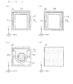
- FIGS. 3 and 4 are plan views showing respective constitutional examples of the imaging element layer 10, the imaging sensor holder layer 20, the infrared cut filter layer 30, the first lens layer 40, the second lens layer 50, the actuator layer 60, the parallel spring lower layer 70, the third lens layer 80, the parallel spring upper layer 90 and the protective layer CB.
- Imaging element layer 10
- the imaging element layer 10 is a chip which is provided with an imaging element part 11 that is formed, for example, of a CMOS sensor, a CCD sensor or the like, a peripheral circuit thereof, and a peripheral part F1 that surrounds the imaging element part 11.
- an imaging element part 11 that is formed, for example, of a CMOS sensor, a CCD sensor or the like, a peripheral circuit thereof, and a peripheral part F1 that surrounds the imaging element part 11.
- a variety of terminals for connecting wiring for providing the imaging element part 11 with a signal and reading the signal from the imaging element part 11 are provided on the rear surface (-Z side surface) of the imaging element layer 10.
- minute holes (through holes) Ca1, Cb1 penetrating along the Z direction are provided, and the through holes Ca1, Cb1. are filled with a material with conductivity (a conductive material). Inner diameters of the minute through holes Ca1, Cb1 are set, for example, to the order of several tens of ⁇ m.
- the +Z side surface of the imaging element part 11 functions as a surface (imaging surface) that receives light from a subject, and the peripheral part F1 is joined to the imaging sensor holder layer 20 adjacent to the +Z side of the imaging element layer 10.
- Imaging sensor holder layer 20
- the imaging sensor holder layer 20 is a chip which is formed, for example, of a material such as a resin and holds the imaging element layer 10 mounted thereon by joining. Specifically, at the substantially center of the imaging sensor holder layer 20, an opening 21 having a substantially square cross section is provided along the Z direction, and the cross section of the opening 21 become smaller toward the +Z side. In addition, the square drawn by broken lines in FIG. 3(b) shows an outer edge of the opening 21 on the -Z side surface.
- the imaging element layer 10 at two predetermined points of a peripheral part of the imaging sensor holder layer 20, minute holes (through holes) Ca2, Cb2 penetrating along the Z direction are provided, and the through holes Ca2, Cb2 are filled with the conductive material. Moreover, the -Z side surface of the peripheral part of the imaging sensor holder layer 20 is joined to the adjacent imaging element layer 10, and the +Z side surface of the peripheral part is joined to the adjacent infrared cut filter layer 30.
- the infrared cut filter layer 30 is a chip of a filter which is configured by multi-layering of transparent thin films with different refractive indexes on a transparent substrate, and cuts infrared rays.
- the infrared cut filter layer 30 is one where a large number of transparent thin films with different refractive indexes are formed on the upper surface of a substrate that is made up, for example, of glass or a transparent resin by sputtering or some other means, and a wave length band of transmitted light is controlled by combination of thicknesses and refractive indexes of the thin films.
- the infrared cut filter layer 30 one that blocks light with a wavelength band of not smaller than 600 nm is preferred.
- the imaging element layer 10 at two predetermined points of a peripheral part of the infrared cut filter layer 30, minute holes (through holes) Ca3, Cb3 penetrating along the Z direction are provided, and the through holes Ca3, Cb3 are filled with the conductive material.
- the -Z side surface of the peripheral part of the infrared cut filter layer 30 is joined to the adjacent imaging sensor holder layer 20, and the +Z side surface of the peripheral part is joined to the adjacent first lens layer 40.
- the first lens layer 40 is a chip which is formed by integral molding of a lens part 41 that is made up of an optical lens having a positive lens power, and a frame part F4 that surrounds the lens part 41 and constitutes a peripheral part of the first lens layer 40, using the same material.
- the material to constitute the first lens layer 40 include a phenolic resin, an acrylic resin, and glass.
- the lens part 41 is an optical lens which refracts light such that a focus by the first to third lens layers 40, 50, 80 corresponds to the imaging element part 11.
- the frame part F4 at predetermined two points of the frame part F4, minute holes (through holes) Ca4, Cb4 penetrating along the Z direction are provided, and the through holes Ca4, Cb4 are filled with the conductive material. Moreover, the -Z side surface of the frame part F4 is joined to the adjacent infrared cut filter layer 30, and the +Z side surface of the frame part F4 is joined to the adjacent second lens layer 50.
- the second lens layer 50 is a chip which is formed by integral molding of a lens part 51 that is made up of an optical lens having a negative lens power, and a frame part F5 that surrounds the lens part 51 and constitutes a peripheral part of the second lens layer 50, using the same material.
- the material to constitute the second lens layer 50 include a phenolic resin, an acrylic resin, and glass.
- the lens part 51 is an optical lens which reflects light such that the focus by the first to third lens layers 40, 50, 80 corresponds to the imaging element part 11.
- the frame part F5 at two predetermined points of the frame part F5, minute holes (through holes) Ca5, Cb5 penetrating along the Z direction are provided, and the through holes Ca5, Cb5 are filled with the conductive material.
- the -Z side surface of the frame part F5 is joined to the adjacent first lens layer 40 (specifically, the frame part F4), and the +Z side surface of the frame part F5 is joined to the adjacent actuator layer 60.
- the actuator layer 60 is a chip which is disposed at the imaging surface side of the imaging element layer 10, while being provided with thin plate-like actuator parts 61a, 61b that move a lens part 81 of the third lens layer 80.
- an element (actuator element) for displacement is formed in the shape of a thin plate on a substrate made of silicon (Si).
- a shape-memory alloy (SMA) is used as the actuator element.
- the actuator layer 60 is provided with a frame part F6 constituting a peripheral part, and the two plate-like actuator parts 61a, 61b projected from the frame part F6 toward a hollow portion inside the frame part F6.
- one ends of the two actuator parts 61a, 61b are respectively fixedly provided on the frame part F6, and the frame part F6 is formed so as to surround the two actuator parts 61a, 61b.
- the frame part F6 is formed by disposition of four plate-like members in square shape which are made up of two plate-like members extendedly provided in parallel with the X axis and forming two mutually opposing sides, and two plate-like members extendedly provided in parallel with the Y axis and forming two mutually opposing sides.
- the one end of the actuator part 61a is fixedly provided on a predetermined part in the vicinity of the -X side end part (the one end) (hereinafter referred to as "one predetermined part")
- the one end of the actuator part 61b is fixedly provided on a predetermined part in the vicinity of the +X side end part (the other end) (hereinafter referred to as "the other predetermined part").
- the respective one ends of the two actuator parts 61a, 61b are ends fixed to the frame part F6 (fixed ends), and the respective other ends of the two actuator parts 61a, 61b are ends whose relative positions to the frame part F6 are freely changed (free ends).
- minute hole parts Ca6, Cb6 are provided along the Z direction from the rear surface (herein, the -Z side surface) of the frame part F6 to the middle of the frame part F6. Moreover, the -Z side surface of the frame part F6 is joined to the adjacent second lens layer 50 (specifically, the frame part F5), and the +Z side surface of the frame part F6 is joined to the adjacent parallel spring lower layer 70.
- FIG. 5 is a view for explaining the detailed configuration of the actuator layer 60.
- the actuator layer 60 is configured by lamination of an insulating layer 602 shown in FIG. 5(b) , a first actuator element layer 603 shown in FIG. 5(c) , an insulating/conductive layer 604 shown in FIG. 5(d) , and a second actuator element layer 605 shown in FIG. 5(e) in this order on a base layer 601 shown in FIG. 5(a) .
- the base layer 601 is made up, for example, of a material with appropriate rigidity (e.g. silicon, metal, etc.), and is made up of a plate-like base member having a frame part 61 and protruding parts 611a, 611b.
- a material with appropriate rigidity e.g. silicon, metal, etc.
- the frame part F61 is a portion to be joined and fixed to the second lens layer 50.
- This protruding part 611a is a plate-like portion protruded from one predetermined part of the frame part F61
- the protruding part 611b is a plate-like portion protruded from the other predetermined portion of the frame part F61.
- the respective one ends of the protruding parts 611a, 611b are fixedly provided on the frame part F61 to be the fixed ends, and the respective other ends of the protruding parts 611a, 611b are free ends, and the frame part F61 is formed so as to surround the protruding parts 611a, 611b.
- minute through holes Ca61, Cb61 are provided along the Z direction, and the through holes Ca61, Cb61 are filled with the conductive material.
- the insulating layer 602 is made up of a material without conductivity (e.g. organic substance), and has the identical shape to that of the base layer 601.
- This insulating layer 602 is formed, for example, of an organic substance with a predetermined thickness by vapor deposition using a mask, or the like over the upper surface (+Z side surface) of the base layer 601. Therefore, the insulating layer 602 has a film-like frame part F62 formed on the upper surface of the frame part F61, and protruding parts 612a, 612b respectively formed on the upper surfaces of the protruding parts 611a, 611b.
- the frame part F6 of the actuator layer 60 is configured primarily of the frame parts F61, F62 which are laminated vertically. Further, at predetermined two points of the frame part F62 (similar positions to those of the imaging element layer 10 and the like), minute through holes Ca62, Cb62 along the Z direction are provided, and the through holes Ca62, Cb62 are filled with the conductive material.
- a technique of forming an insulating layer on the base layer 601 not provided with the through holes Ca61, Cb61 and then simultaneously forming the minute through holes Ca61, Cb61, Ca62, Cb62 by such a means as embossing is preferred.
- the first actuator element layer 603 has two displacement element parts 613a, 613b and two electrode parts Ta, Tb.
- the displacement element part 613a is provided on the protruding parts 611a, 612a, and made up of a thin plate-like element (herein, the shape-memory alloy) that expands and contracts in accordance with application of a voltage.
- the displacement element part 613b has a similar shape to that of the displacement element part 613a, and is provided on the protruding parts 611b, 612b, and made up of a thin plate-like element (herein, the shape-memory alloy) that expands and contracts in accordance with application of a voltage.
- the displacement element parts 613a, 613b are formed, for example, by film formation by means of sputtering, or formed by joining of elements having been stretched into frame shape with use of an adhesive or the like.
- the electrode part Ta is a portion that is made up, for example, of a metal excellent in conductivity, or the like and electrically connected to the vicinity of the end part of one predetermined part side (a fixed end) within the displacement element part 613a, to apply a voltage supplied from the conductive material with which the through holes Ca61, Ca62 are filled to the displacement element part 613a.
- the electrode part Ta is provided directly on the through hole Ca62.
- the electrode part Tb is a portion that is made up, for example, of metal excellent in conductivity, or the like and electrically connected to the vicinity of the end part of the other predetermined part side (a fixed end) within the displacement element part 613b, to apply the voltage supplied from the conductive material with which the through holes Cb61, Cb62 are filled to the displacement element part 613b.
- the electrode part Tb is provided directly on the through hole Cb62.
- the insulating/conductive layer 604 has insulating films 614a, 614b and conductor parts Cna, Cnb.
- the insulating film 614a is a film without electric conductivity (an insulating film) which is provided in the shape of a thin film over the entire area from the fixed end to a position slightly before the free end within the upper surface of the displacement element part 613a.
- the insulating film 614b is a film without electric conductivity (an insulating film) which is provided in the shape of a thin film over the entire area from the fixed end to a position slightly before the free end within the upper surface of the displacement element part 613b.
- These insulating films 614a, 614b are formed, for example, by vapor deposition of an organic substance using a mask, or some other means.
- the conductor part Cna is a film with electric conductivity (a conductive film) which is provided in the vicinity of the end part of the opposite side to the one predetermined part (a free end) within the upper surface of the displacement element part 613a.
- the conductor part Cnb is a conductive film provided in the vicinity of the end part of the opposite side to the other predetermined part (a free end) within the upper surface of the displacement element part 613b.
- the conductor parts Cna, Cnb are formed by film formation, for example, by means of sputtering or the like.
- the second actuator element layer 605 has two the displacement element parts 615a, 615b, and a connector part 615c.
- the displacement element parts 615a, 615b are made up of a material similar to those for the displacement element part 613a, 613b and formed, for example, by film formation by means of sputtering, or formed by joining of elements having been stretched into frame shape with use of an adhesive or the like.
- the displacement element part 615a is provided almost over the upper surfaces of the insulating film 614a and the conductor part Cna
- the displacement element part 615b is provided almost over the upper surfaces of the insulating film 614b and the conductor part Cnb.
- the displacement element part 613a and the displacement element part 615a are formed so as to sandwich the insulating film 614a and the conductor part Cna therebetween, and the displacement element part 613a and the displacement element part 615a are electrically connected by the conductor part Cna in the vicinity of the free end. Further, the displacement element part 613b and the displacement element part 615b are formed so as to sandwich the insulating film 614b and the conductor part Cnb therebetween, and the displacement element part 613b and the displacement element part 615b are electrically connected by the conductor part Cnb in the vicinity of the free end.
- the connector part 615c is wiring which is provided on the upper surface side of the frame part F61 (specifically, the upper surface of the frame part F62), and electrically connects the displacement element part 615a and the displacement element part 615b in the vicinity of the fixed ends.
- This connector part 615c is made up, for example, of a metal excellent in conductivity, or the like, and formed by film formation by means of sputtering, or the like.
- displacement element parts 613a, 613b, 615a, 615b are subjected to heat treatment to memorize shapes (memory heat treatment) on a timely basis so as to be shrunk during heating.
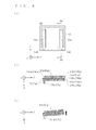
- FIG. 6 is a view for explaining the operation of the actuator part 61b.
- FIG. 6(a) is a plan view showing a configuration of the actuator layer 60 as with FIG. 3(f)
- FIGS. 6(b) and 6(c) are sectional diagrammatic views focusing on the actuator part 61b, as seen from a sectional line 6A-6A of FIG. 6(a) .
- wiring CTb is shown which is formed by filling of the through holes Cb1 to Cb5, Cb61, Cb62 with the conductive material.
- the wiring CTb is electrically connected to the displacement element part 613b through the electrode part Tb, and a voltage is applied from a power circuit (not shown) of the body 300 to the actuator part 61b through the wiring CTb.
- the wiring CTa formed by filling of the through holes Ca1 to Ca5, Ca61, Ca62 with the conductive material is electrically connected to the displacement element part 613a through the electrode part Ta, and a voltage is applied from the power circuit to the actuator part 61a through the wiring CTa.
- nine portions constituting the two actuator parts 61a, 61b i.e. the electrode part Ta, the displacement element part 613a, the conductor part Cna, the displacement element part 615a, the connector part 615c, the displacement element part 615b, the conductor part Cnb, the electrode part Tb and the displacement element part 615b, are connected in this order in series between the wiring CTa, CTb.
- FIG. 6(b) a state (initial state) where the actuator part 61b has not been transformed is shown.
- the initial state the voltage has not been applied to the displacement element parts 613b, 615b, and the displacement element parts 613b, 615b are in a constant-temperature state. Therefore, the displacement element parts 613b, 615b are formed into plate shape by elastic force of the protruding part 611b of the base layer 601, and the actuator part 61b takes almost flat shape.
- the extended distances of the displacement element parts 613b, 615b return to the initial states by natural cooling, and the actuator part 61b returns to the initial state of not being transformed.
- the two actuator parts 61a, 61b are electrically connected by the connector part 615c, and simultaneously energized and heated. For this reason, the two actuator parts 61a, 61b are transformed in substantially the same timing and mechanism into substantially the same shape.
- the parallel spring lower layer 70 is a chip which is made up of a metal material such as phosphor bronze and has the frame part F7 and the elastic part 71, and is a layer forming a spring mechanism (an elastic layer).
- the frame part F7 constitutes a peripheral part of the parallel spring lower layer 70.
- the -Z side surface of the frame part F7 is joined to the adjacent actuator layer 60 (specifically, the frame part F6), and the +Z side surface of the frame part F7 is joined to the adjacent third lens layer 80.
- the elastic part 71 is formed by connection in U shape of three plate-like members 71a, 71b, 71c, that substantially linearly extend, and respective one ends of the two plate-like members 71a, 71c on both sides among the three plate-like members 71a, 71b, 71c, namely both ends of the elastic part 71, are fixedly provided at two points of the frame part F7.
- the elastic part 71 is disposed in a hollow portion inside the frame part F7, and hence the frame part F7 is formed so as to surround the elastic part 71.
- the frame part F7 is formed by disposition of four plate-like materials in square shape which are made up of two plate-like members extendedly provided in parallel with the X axis and forming two mutually opposing sides, and two plate-like members extendedly provided in parallel with the Y axis and forming two mutually opposing sides.
- the one end of the elastic part 71 (specifically, one end of the plate-like member 71a) is fixedly provided on a predetermined part in the vicinity of the -X side end part (one end) (hereinafter referred to as "one predetermined part"), and the one end of the elastic part 71 (specifically, one end of the plate-like member 71c) is fixedly provided on a predetermined part in the vicinity of the +X side end part (the other end) (hereinafter referred to as "the other predetermined part").
- the lower surfaces (-Z side surfaces) of the two plate-like members 71a, 71c on both sides among the three plate-like members 71a, 71b, 71c constituting the elastic part 71 are in contact with the upper surfaces (+Z side surfaces) of the actuator parts 61a, 61b. Therefore, in accordance with transformation of the actuator parts 61a, 61b shown in FIG. 6 , the two plate-like members 71a, 71c are elastically transformed such that a relative position of the plate-like member 71b with respect to the frame part F7 is shifted to the +Z side.
- the third lens layer 80 is a chip which has a frame part F8, a lens part 81 and a lens holder 83.
- Examples of the material to constitute this third lens layer 80 include a phenolic resin, an acrylic resin, and glass, as with the cases of the first and second lens layers 40, 50.
- the frame part F8 constitutes a peripheral part of the third lens layer 80.
- the frame part F8 is formed by disposition of four plate-like materials in square shape which are made up of two plate-like members extendedly provided in parallel with the X axis and forming two mutually opposing sides, and two plate-like members extendedly provided in parallel with the Y axis and forming two mutually opposing sides.
- the lens part 81 and the lens holder 83 are disposed in a hollow portion formed inside the frame part F8, and hence the lens part 81 and the lens holder 83 are in the state of being surrounded by the frame part F8.
- the -Z side surface of the frame part F8 is joined to the adjacent parallel spring lower layer 70 (specifically, the frame part F7), and the +Z side surface of the frame part F8 is joined to the adjacent parallel spring upper layer 90.
- the lens part 81 is an optical lens whose distance from the imaging element part 11 is changeable, and herein has positive lens power.
- the lens holder 83 holds the lens part 81, and held between the elastic part 71 of the parallel spring lower layer 70 and a elastic part 91 of the later-described parallel spring upper layer 90.
- the lens holder 83 is integrally molded with the lens part 81, and within the end part of +Y side of the lens holder 83, the -Z side surface is joined with the elastic part 71 and the +Z side surface is joined with the elastic part 91.
- couplers 84a, 84b drawn by a thick broken line in FIG. 4(b) are cut in the middle of manufacturing of the camera module 400, and the frame part F8, the lens part 81 and the lens holder 83 come into a separated state, to form the third lens layer 80.
- the cutting of the couplers 84a, 84b will be further described later.
- the parallel spring upper layer 90 is a chip having a similar configuration as that of the parallel spring lower layer 70, the chip being made up of a metal material such as phosphor bronze and having the frame part F9 and the elastic part 91, and is a layer (elastic layer) forming a spring mechanism.
- the frame part F9 constitutes a peripheral part of the parallel spring lower layer 90.
- the -Z side surface of the frame part F9 is joined to the adjacent third lens layer 80 (specifically, the frame part F8), and the +Z side surface of the frame part F9 is joined to the adjacent protective layer CB.
- the elastic part 91 is formed by connection in U shape of three plate-like members 91a, 91b, 91c, that substantially linearly extend, and respective one ends of the two plate-like members 91a, 91c on both sides among the three plate-like members 91a, 91b, 91c, namely both ends of the elastic part 91, are fixedly provided at two points of the frame part F9.
- the elastic part 91 is disposed in a hollow portion inside the frame part F9, and hence the frame part F9 is formed so as to surround the elastic part 91.
- a more specific configuration of the frame part F9 is similar to that of the frame part F7 described above, and hence a description thereof is omitted herein.
- the lower surface (-Z side surface) of the one plate-like member 91b at the center among the three plate-like members 91a, 91b, 91c constituting the elastic part 91 is joined to the lens holder 83, whereby the lens holder 83 is held between the elastic part 71 and the elastic part 91.
- the two plate-like members 91a, 91c are elastically transformed such that a relative position of the plate-like member 91b with respect to the frame part F9 is shifted to the +Z side.
- the protective layer CB is a plate-like transparent member with its board surface in substantially square shape and is made up, for example, of a resin, glass, or the like.
- the -Z side surface of a peripheral part of the protective layer CB is joined to the adjacent parallel spring upper layer 90 (specifically, the frame F9).
- the peripheral part of the protective layer CB may be structured, for example, to have a convex shape along the periphery, and joined on the upper end surface in convex shape.
- FIG. 7 is a view showing a structure of the camera module 400.
- FIG. 7(a) is a plan view of the camera module 400 seen from the protective layer CB side (the top)
- FIG. 7(b) is a sectional diagrammatic view seen from a section line 7A-7A of FIG. 7(a) .
- one through hole Cva formed by linkage of the through holes Ca1 to Ca5, Ca61, Ca62 and one through hole Cvb formed by linkage of the through holes Cb1 to Cb5, Cb61, Cb62, which are located on the -Y side more closely than the section are indicated by dotted lines so that positional relations of the respective holes can be seen.
- the camera module 400 is formed by lamination of the imaging element layer 10, the imaging sensor holder layer 20, the infrared cut filter layer 30, the first lens layer 40, the second lens layer 50, the actuator layer 60, the parallel spring lower layer 70, the third lens layer 80, the parallel spring upper layer 90 and the protective layer CB in this order. Further, the through holes Cva, Cvb are each filled with the conductive material, to provide the actuator parts 61a, 61b of the actuator layer 60 with a voltage supplied from the rear surface (-Z side surface) of the imaging element layer 10.
- this camera module 400 is manufactured, for example, by micromachining technique that is used for integration of a micro device.
- this technique is generally termed MEMS (Micro Electro Mechanical System).
- MEMS Micro Electro Mechanical System
- fields where the name of the processing technique, MEMS, is used include fields where a micro sensor, an actuator, and an electromechanical structure with sizes on the order of ⁇ m are manufactured through use of the micro machining technique to which a semiconductor process, and especially an integrated circuit technique, has been applied.
- a manufacturing method for the camera module 400 will be further described later.
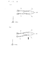
- FIG. 8 is a view for explaining a driving aspect of the lens part 81 included in the third lens layer 80.
- FIG. 8 shows a diagrammatic view of states of the lens part 81 and the elastic parts 71, 91 seen from the side. It is to be noted that, although the lens holder 83 is in practice held between the elastic parts 71 and 91, FIG. 8 shows the lens part 81 being held by the elastic parts 71, 91 at points Pu, Pd, for the sake of simplifying a description. Further, FIG. 8(a) shows a state (initial state) of the elastic parts 71, 91 having not been transformed, and FIG. 8(b) shows a state (transformed state) of the elastic parts 71, 91 having been transformed.
- the elastic parts 71, 91 have similar configurations to each other, and respectively fixedly provided at two points of the frame parts F7, F9 in similar manners to each other.
- the elastic part 71 transforms by transformation of the actuator parts 61a, 61b such that the plate-like member 71b rises
- the elastic part 91 similarly transforms through the lens part 81. This is identifiable to a state where the lens part 81 is held between the plate-like members 71a, 91a and the plate-like members 71c, 91c which are provided in parallel at intervals of predetermined distances, and the plate-like members 71a, 91a and the plate-like members 71c, 91c perform substantially the same transformation in substantially the same timing.
- the lens part 81 moves in a vertical direction (herein, the direction along the Z-axis) without inclination of an optical axis.
- a distance between the lens part 81 and the imaging element part 11 can be changed without displacement of the direction of the optical axis of the lens part 81. Consequently, the distance between the imaging element part 11 and the lens part 81 is changed, to execute focus adjustment.
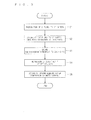
- FIG. 9 is a flowchart illustrating manufacturing process for the camera module 400.
- the camera module 400 is manufactured by sequential performance of: (Step A) preparation of a plurality of sheets (Step S1); (Step B) joining of the plurality of sheets (Step S2); (Step C) dicing (Step S3); (Step D) inspection of eccentricity of an optical axis (Step S4); and (Step E) binding of an imaging element layer (Step S5).
- Step A preparation of a plurality of sheets
- Step S2 joining of the plurality of sheets
- Step S3 dicing
- Step D inspection of eccentricity of an optical axis
- Step E binding of an imaging element layer
- Step A Preparation of a plurality of sheets
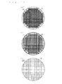
- FIGS. 10 and 11 are plan views showing constitutional examples of ten sheets U2 to U9, UCB to be prepared. Herein, a description will be given showing an example of each of the sheets U2 to U9, UCB being in disk shape.
- FIG. 10(a) is a view illustrating a sheet (imaging sensor holder sheet) U2 where a large number of chips corresponding to the imaging sensor holder layers 20 shown in FIG. 3(b) are formed in a predetermined array (herein, a matrix-like predetermined array).
- a predetermined array is used in the meaning of including a state where a large number of chips are arrayed at predetermined intervals in a predetermined direction.
- this imaging sensor holder sheet U2 is manufactured, for example, with use of a resin material as a material by pressing with a metal mold.
- the through holes Ca2, Cb2 are formed, for example, by embossing, etching or the like.
- each imaging sensor holder layer 20 corresponds to a predetermined member to which the imaging element layer 10 having the imaging element part 11 is attached.
- FIG. 10(b) is a view illustrating a sheet (infrared cut filter sheet) U3 where a large number of chips corresponding to the infrared cut filter layers 30 shown in FIG. 3(c) are formed in the predetermined array (herein, the matrix-like predetermined array).
- This infrared cut filter sheet U3 is manufactured, for example, by multi-layering of transparent thin films with different refractive indexes on a transparent substrate. Specifically, the sheet is manufactured by first preparing a substrate of glass or a transparent resin to be a substrate of the filter, and then laminating a large number of transparent thin films with different refractive indexes on the upper surface of the substrate by a technique such as sputtering or vapor deposition.
- making an appropriate change in combination of the thicknesses or the refractive indexes of the transparent thin films can set a wavelength band of transmitted light.
- a setting is made such that light with a wavelength band of not smaller than 600 nm is prevented from being transmitted, to block infrared light.
- the through holes Ca3, Cb3 are formed, for example, by embossing, etching or the like.
- FIG. 10(c) is a view illustrating a sheet (first lens sheet) U4 where a large number of chips corresponding to the first lens layers 40 shown in FIG. 3(d) are formed in the predetermined array (herein, the matrix-like predetermined array)
- FIG. 10(d) is a view illustrating a sheet (second lens sheet) U5 where a large number of chips corresponding to the second lens layers 50 shown in FIG. 3(e) are formed in the predetermined array (herein, the matrix-like predetermined array).
- the first and second lens sheets U4, U5 are manufactured, for example, with use of a phenolic resin, an acrylic resin or optical glass as a material by a technique such as molding or etching.
- the through holes Ca4, Ca5, Cb4, Cb5 are formed, for example, by embossing, etching, or the like.
- a thin film of a lightproof material may be formed on the second lens layers 50 and the like using a shadow mask, or a diaphragm may be formed of a resin material separately colored black, or the like.
- FIG. 10(e) is a view illustrating a sheet (actuator sheet) U6 where a large number of chips corresponding to the actuator layers 60 shown in FIG. 3(f) are formed in the predetermined array (herein, the matrix-like predetermined array).
- the actuator sheet U6 is manufactured, for example, by formation of a thin film of the shape-memory alloy (SMA) corresponding to an actuator element on a substrate of silicon (Si) or the like.
- SMA shape-memory alloy
- etching is performed as appropriate on a thin plate of silicon (or a metal), to form a base plate where a large number of base layers 601 ( FIG. 5(a) ) are formed in the predetermined array (herein, the matrix-like predetermined array).
- the through holes Ca61, Ca62, Ca61, Cb61 are formed, for example, by embossing, etching, or the like. Further, at this time, a hole portion Ca6 formed by integral linkage of the through holes Ca61, Ca62 and a hole portion Cb6 formed by integral linkage of the through holes Cb61, Cb62 are plated with a metal.
- the through holes Ca61, Cb61 may, for example, be formed by etching such as DRIE (Deep Reactive Ion Etching) on the thin plate of silicon.
- the actuator element layer 603 ( FIG. 5(c) ) is formed, for example, by means of sputtering (or vapor deposition). At this time, the displacement element parts 613a, 613b and the electrode parts Ta, Tb come into the state of being formed on each insulating layer 602.
- the insulating/conductive layer 604 ( FIG. 5(d) ) is formed by formation of an insulating film by means of photolithography and formation of a metal thin film by means of sputtering (or vapor deposition). At this time, the insulating films 614a, 615b and the conductor parts Cna, Cnb come into the state of being formed on the displacement element parts 613a, 613b and the electrode parts Ta, Tb.
- the second actuator element layer 605 ( FIG. 5(e) ) is, for example, formed by means of sputtering (or vapor deposition).
- the displacement element parts 615a, 615b come into the state of being formed on the insulating films 614a, 615b and the conductor parts Cna, Cnb, while the connector part 615c that connects the displacement element parts 615a, 615b in a conductible manner comes into the state of being formed.
- the actuator parts 61a, 61b are then set into a mold of a shape wished to be memorized, which are then subjected to treatment (shape-memory treatment) of heating at a predetermined temperature (e.g. 600°C).
- FIG. 10(f) is a view illustrating a sheet (parallel spring lower sheet) U7 where a large number of chips corresponding to the parallel spring lower layers 70 shown in FIG. 4(a) are formed in the predetermined array (herein, the matrix-like predetermined array)
- FIG. 11(b) is a view illustrating a sheet (parallel spring upper sheet) U9 where a large number of chips corresponding to the parallel spring upper layers 90 shown in FIG. 4(c) are formed in the predetermined array (herein, the matrix-like predetermined array).
- the parallel spring lower sheet U7 and the parallel spring upper sheet U9 are manufactured, for example, by performing etching or the like on a thin plate of a metal material such as phosphor bronze.
- FIG. 11(a) is a view illustrating a sheet (third lens sheet) U8 where a large number of chips corresponding to the third lens layers 80 shown in FIG. 4(b) are formed in the predetermined array (herein, the matrix-like predetermined array).
- the third lens sheet U8 are manufactured, for example, with use of a phenolic resin, an acrylic resin, or optical glass as a material by a technique such as molding or etching.
- FIG. 11(c) is a view illustrating a sheet (protective sheet) UCB where a large number of chips corresponding to the protective layers CB shown in FIG. 4(d) are formed in the predetermined array (herein, the matrix-like predetermined array).
- the protective sheet UCB is, for example, a plate-like sheet manufactured by making a resin (glass) as a transparent material have a desired thickness, and performing etching as appropriate.
- marks for alignment in the sheet joining step are put in substantially the same positions.
- the alignment mark include a mark such as a cross, and the marks are preferably provided at two or more positions which are in the vicinity of the peripheral part of the upper surface of each of the sheets U2 to U9, UCB, and relatively separated.
- FIG. 12 is a view diagrammatically showing a step of sequentially laminating and joining the plurality of sheets U2 to U9, UCB.
- the imaging sensor holder sheet U2, the infrared cut filter sheet U3, the first lens sheet U4 and the second lens sheet U5 are subjected to alignment while remaining in sheet form such that chips of each of the sheets U2 to U5 are laminated immediately on one another.
- a displacement amount (i.e. eccentricity accuracy) of optical axes of the three lens parts 41, 51, 81 are desirably within 5 ⁇ m.
- the imaging sensor holder sheet U2 and the infrared cut filter sheet U3 are first set in a known aligner, and alignment is performed using previously formed alignment marks.
- a so-called epoxy resin adhesive or ultraviolet cure adhesive is previously applied on a surface (joining surface) where the imaging sensor holder sheet U2 and the infrared cut filter sheet U3 are to be joined, and both sheets U2, U3 are joined.
- a method may be used in which the joining surface is irradiated with O 2 plasma to activate the joining surface so as to directly join the sheets U2 and U3.
- the first lens sheet U4 is joined onto the infrared cut sheet U3, and further, the second lens sheet U5 is joined onto the first lens sheet U4.
- the actuator sheet U6 On the upper surface of a laminated body formed by lamination of the four sheets U2 to U5, the actuator sheet U6, the parallel spring lower sheet U7, the third lens sheet U8 and the parallel spring upper sheet U9 are laminated and joined in this order sequentially from the bottom. Alignment and joining methods are similar to the techniques according to the foregoing sheets U2, U3, and at this time, each chip of the sheets U2 to U9 is laminated immediately on one another.
- the lens part 81 of the third lens sheet U8 comes into the state of being supported by the actuator parts 61a, 61b of the actuator sheet U6 through the elastic part 71 of the parallel spring lower sheet U7. Further, with the sheets U7 to U9 laminated and bound, the lens holder 83 is held between the elastic parts 71, 91 from the upper and lower surfaces, and the lens part 81 comes into the state of being supported by the elastic parts 71, 91.
- the couplers 84a, 84b (cf. FIG. 4(b) ) that couple the frame part F8 and the lens part 81 through the lens holder 83 are cut by a so-called femtosecond laser or the like, to separate the frame part F8 and the lens part 81.
- the lens part 81 in each chip is supported by the elastic parts 71, 91, and thereafter brought into a movable state. It is thus possible to perform precise alignment of the lens part 81 and the actuator parts 61a, 61b. In other words, for example, it is possible to prevent eccentricity of the optical axis of the lens part in each optical unit (later described), and the like.
- the protective sheet UCB is aligned and joined to the upper surface of the parallel spring upper sheet U9 in a similar manner to the foregoing technique.
- a member laminated member
- the formed laminated member where the nine sheets U2 to U9, UCB are laminated are cut with respect to each chip by means of a dicing device, to generate a large number of optical system units (optical units) where the nine layers 20 to 90 and CB are laminated.
- the large number of optical units generated by dicing are inspected with lens eccentricity measuring instrument as to whether or not displacement amounts (i.e. eccentricity) of the optical axes of the three lens parts 41, 51, 81 are within a predetermined tolerance range (e.g. within 5 ⁇ m).
- the highest-priced one among the components constituting the camera module 400 is the imaging element layer 10.
- the camera module 400 with the eccentricity of the optical axis being out of the predetermined tolerance range is treated as a defective product. Therefore, sorting-out for defective and non-defective products is performed at the stage of the optical unit and the imaging element layer 10 is mounted only on a non-defective product, whereby it is possible to seek reduction in manufacturing cost of the camera module 400 and waste of resources.
- each optical unit discriminated as a non-defective product by the inspection of eccentricity of the optical axis (specifically, the rear surface of the imaging sensor holder layer 20) is mounted with the chip of the imaging element layer 10 by joining with use of a so-called epoxy resin adhesive or ultraviolet cure adhesive, to complete the camera module 400.
- the camera module 400 is formed by lamination of the plurality of layers 10 to 90, CB which include the imaging element layer 10, the third lens layer 80 and the actuator layer 60. Hence it is possible to satisfy both higher functionality and higher accuracy in a compact imaging device.
- the adjacent layers included in the plurality of layers 10 to 90, CB constituting the camera module 400 are joined on the peripheral part F1 and the frame parts F4 to F9. This can facilitate sealing of the imaging element part 11, the lens parts 41, 51, 81 and the actuator parts 61a, 61b.
- each optical unit is separated. It is therefore possible to readily and accurately combine members that realize a plurality of functions. In other words, it is possible to satisfy both higher functionality and higher accuracy in a compact imaging device.
- the imaging element layer 10 is mounted. It is therefore possible to reduce wasteful disposal of the imaging element part 11 associated with failure of the optical unit. In other words, it is possible to reduce manufacturing cost of the imaging device and waste of resources.
- the camera module 400 is formed by lamination of ten layers, but this is not restrictive.
- the third lens layer 80 considered can be a configuration where the lens part 81 having the lens power and the frame part F8 are linked by a thin plate-like elastic member formed of the same material as that for the lens part 81 at at least two points around the lens part 81, and the parallel spring lower layer 70 and the parallel spring upper layer 90 are thereby omitted.
- the third lens layer 80 one formed by linkage of the frame part F8 and the lens part 81 by at least three elastic members from different directions around the lens part 81 may be adopted.
- the places provided with three or more elastic members are desirably places where the frame part F8 can support the lens part 81 in a balanced manner, such as substantially evenly spaced positions along direction of a circumference with the optical axis of the lens part 81 at the center.
- the other layers 70, 90 having the elastic parts 71, 91 for holding the lens part 81 become unnecessary, whereby it is possible to seek improvement in assembly accuracy due to simplification of the structure of the imaging device 400, and reduction in thickness and size of the imaging device 400.
- the first and second lens layers 40, 50 can also be omitted as appropriate depending upon a design of the optical system. Therefore, from the viewpoint of accurately supporting the lens part 81 by the actuator part, the camera module 400 may be formed by lamination of a plurality of layers at least including the lens layer 80 that has the moving lens part 81 and the actuator layer 60 that moves the lens part 81.
- the eccentricity of the optical axis of the optical unit is inspected after dicing and the imaging element layer 10 is mounted on a non-defective optical unit, but this is not restrictive.
- a sheet (image element sheet) formed with a large number of imaging element layers 10 shown in FIG. 3(a) in the predetermined array may be previously formed on a predetermined substrate (e.g.
- the imaging element sheet is aligned, laminated and joined along therewith, and thereafter, dicing may be performed, so as to complete a large number of camera modules 400.
- Adopting such a configuration facilitates alignment at the time of joining the imaging element layer 10, whereby it is possible to readily and accurately combine members that realize a plurality of functions, including the imaging element part 11.
- the through hole formed by integral linkage of the through holes Ca2 to Ca5 and the through hole formed by integral linkage of the through holes Cb2 to Cb5 are plated with a metal to form wiring, but this is not restrictive.
- the through hole formed by integral linkage of the through holes Ca1 to Ca5, Ca61, Ca62 and the through hole formed by integral linkage of the through holes Cb1 to Cb5, Cb61, Cb62 may be plated with a metal, to form the wiring CTa, CTb.
- the through holes Ca2 to Ca5, Ca61, Ca62, Cb2 to Cb5, Cb61, Cb62 may be previously filled with a conductive material by being plated with a metal or the like with respect to each sheet, and at the time of laminating the five sheets U2 to U6, the wiring CTa, CTb may be formed.
- the through holes Ca2 to Ca5, Ca61, Ca62, Cb2 to Cb5, Cb61, Cb62 are preferably filled with the conductive material to such a degree that the conductive material slightly run off from the respective holes.
- the wiring CTa, CTb for voltage supply which penetrate the five layers among the ten layers constituting the camera module 400 are provided, but this is not restrictive.
- the wiring penetrating therethrough may not be provided, and similarly to all kinds of wiring for signals disposed inside the imaging element layer 10, wiring for voltage supply may be provided as appropriate within the imaging element layer 10, and a terminal part electrically connectable to the wiring may be provided from the rear surface or the side surface of the imaging element layer 10. Even when such a configuration is adopted, the wiring part for providing the actuator parts with the electric field may be readily and accurately formed as with the above embodiment.
- the first and second lens layers 40, 50 can also be omitted as appropriate depending upon the design of the optical system. Therefore, from the viewpoint of readily and accurately forming the wiring part for providing the actuator parts 61a, 61b with the electric field, there may be provided wiring that penetrates one or more layers which are disposed between the imaging element layer 10 and the actuator layer 60 among the plurality of layers constituting the camera module 400, and provides the actuator layer 60 with the electric field.
- the through holes Ca61, Cb61 are provided in the base layer 601 and then filled with the conductive material, but this is not restrictive, and for example, a silicon thin plate to be a material for the base layer 601 may be subjected to ion doping so as to form a conductible area.
- each of the through holes Ca2 to Ca5, Cb2 to Cb5 penetrating the plurality of sheets U2 to U5 are formed with respect to each sheet, but this is not restrictive.
- a through hole with a size of the order of several tens of ⁇ m penetrating the four sheets may be formed by so-called femtosecond laser or excimer laser, ion etching, or the like.
- the voltage is applied to the actuator parts 61a, 61b by the wiring CTa, CTb that penetrate the plurality of layers, but this is not restrictive.
- wiring for electrically connecting the terminal part disposed on the outer edge of the actuator layer 60 and the actuator parts 61a, 61b may be provided.
- the terminal part functions as a terminal for electrically connecting wiring for providing the electric field from the outside of the actuator layer 60 to the actuator parts 61a, 61b. Adopting such a configuration facilitates formation of each layer disposed between the imaging element layer 10 and the actuator layer 60.
- the shape-memory alloy (SMA) is used as the actuator element, but this is not restrictive, and for example, an piezoelectric element such as an inorganic piezoelectric body of PZT (Pb(lead) zirconate titanate) or the like, or an organic piezoelectric body of polyvinylidene fluoride (PVDF) or the like may be used.
- an electrode the thin film of the piezoelectric element and an electrode may be formed in this order on the base layer 601 by sputtering or the like, and a high electric field may be applied to perform polling.
- the actuator parts 61a, 61b are formed by formation of the thin film of the actuator element on the base layer 601 through the insulating layer 602 and the insulating films 614a, 614b, but this is not restrictive.
- the actuator parts 61a, 61b are formed on the base layer 601 by formation of metal thin films having different rates (linear expansion ratios or linear expansion coefficients) at which the length changes with increase in temperature, as compared with the material for the base layer 601. It is to be noted that as combination of materials having different line expansion coefficients, for example, an aspect of silicon (Si) constituting the base layer and aluminum (Al) constituting the metal thin film can be considered.
- the elastic parts 71, 91 are respectively fixedly provided at two points of the frame parts F7, F9, but this is not restrictive, and a variety of configurations may be applied. However, in order to move the lens part 81 without inclination of the optical axis of the lens 81 as described above, it is preferable that the elastic parts 71, 91 be respectively fixedly provided at two or more points of the frame part F7, F9.
- both ends of the elastic part 71 are fixedly provided to a total of two points of the frame part F7 and both ends of the elastic part 91 are fixedly provided to a total of two points of the frame part F9, but this is not restrictive.
- the elastic parts 71, 91 are respectively dually divided at the center portions and one end and the other end of the dually divided elastic part 71 are respectively fixedly provided on the frame part F7 so as to be fixedly provided at a total of two points, and one and the other end of the dually divided elastic part 91 are respectively fixedly provided on the frame part F9 so as to be fixedly provided at a total of two points.
Landscapes
- Engineering & Computer Science (AREA)
- Physics & Mathematics (AREA)
- Multimedia (AREA)
- Signal Processing (AREA)
- General Physics & Mathematics (AREA)
- Optics & Photonics (AREA)
- General Engineering & Computer Science (AREA)
- Manufacturing & Machinery (AREA)
- Health & Medical Sciences (AREA)
- Ophthalmology & Optometry (AREA)
- Mechanical Engineering (AREA)
- Lens Barrels (AREA)
- Studio Devices (AREA)
- Solid State Image Pick-Up Elements (AREA)
- Camera Bodies And Camera Details Or Accessories (AREA)
- Transforming Light Signals Into Electric Signals (AREA)
Abstract
Description
- The present invention relates to a compact imaging device and a manufacturing method therefor.
- In recent years, a camera module has often been installed in compact electronic equipment such as a mobile telephone, and has been intended to be further reduced in size.
- This camera module has conventionally been required to have a lens barrel and a lens holder that support a lens, a holder that supports an infrared (IR) cut filter, a housing that holds a laminated body made up of a substrate, an imaging element and an optical element, a resin that seals the laminated body, and the like. Therefore, when the above large number of components are sought to be reduced in size, accurately combining the large number of components to produce a camera module has not been easy.
- This being the case, there has been proposed a technique in which a substrate, a semiconductor sheet formed with a large number of imaging elements and a lens array sheet formed with a large number of imaging lenses are attached with resin layers interposed therebetween to form a laminated member, and the laminated member is subjected to dicing, to complete separate camera modules (e.g.,
Patent Document 1, etc). - Patent Document 1: Japanese Patent Application Laid-Open No.
2007-12995 - However, even a compact camera module has been required to have higher functionality by being equipped with a variety of functions such as auto focusing and a zooming function, and the technique of the
foregoing Patent Document 1 is not one capable of sufficiently meeting such a requirement for higher functionality. - The present invention was made in view of the above problem, and an object thereof is to provide a technique capable of satisfying both higher functionality and higher accuracy in a compact imaging device.
- For solving the above problem, an imaging device according to a first aspect is formed by lamination of a plurality of layers including: an imaging element layer that has an imaging element part; a lens layer that has a lens part whose distance from the imaging element part is changeable, and is disposed on an imaging surface side to receive light from a subject within the imaging element part; and an actuator layer that has an actuator part to move the lens part, and is disposed on the imaging surface side of the imaging element part.
- An imaging device according to a second aspect is the imaging device according to the first aspect, wherein the imaging element layer has a peripheral part which surrounds the imaging element part, the lens layer has a first frame part which surrounds the lens part, the actuator layer has a second frame part which is fixedly provided with one end of the actuator part and surrounds the actuator part, the peripheral part is joined to a layer adjacent to the imaging element layer among the plurality of layers, the first frame part is joined to a layer adjacent to the lens layer among the plurality of layers, and the second frame part is joined to a layer adjacent to the actuator layer among the plurality of layers.
- An imaging device according to a third aspect is the imaging device according to the second aspect, wherein the plurality of layers include: a first elastic layer having a third frame part joined with the first frame part from one direction, and a first elastic part fixedly provided at at least two points of the third frame part; and a second elastic layer having a fourth frame part joined with the first frame part from the opposite direction to the one direction, and a second elastic part fixedly provided at at least two points of the fourth frame part, and the lens layer has a lens holder which holds the lens part and is held between the first elastic part and the second elastic part.
- An imaging device according to a fourth aspect is the imaging device according to the second aspect, wherein the lens layer has at least three elastic parts which connect the first frame part and the lens part.
- An imaging device according to a fifth aspect is the imaging device according to the first aspect, and further provided with a wiring part which penetrates one or more layers disposed between the imaging element layer and the actuator layer among the plurality of layers, and provides the actuator layer with an electric field.
- An imaging device according to a sixth aspect is the imaging device according to the first aspect, wherein the actuator layer further has a terminal part which is electrically connected to the actuator part on an outer edge and connects a wiring for providing the actuator part with an electric field.
- An imaging device according to a seventh aspect is the imaging device according to the first aspect, wherein a resin, which joins mutually adjacent two layers included in the plurality of layers, intervenes between the two layers.
- An imaging device according to an eighth aspect is the imaging device according to the first aspect, wherein the actuator part includes a substrate, and a thin film of a shape-memory alloy which is formed on the substrate.
- An imaging device according to a ninth aspect is the imaging device according to the first aspect, wherein the actuator part includes a substrate, and a thin film of a piezoelectric element which is formed on the substrate.
- An imaging device according to a tenth aspect is the imaging device according to the first aspect, wherein the actuator part includes a substrate, and a metal thin film which is formed on the substrate and has a linear expansion coefficient different from that of the substrate.
- An imaging device manufacturing method according to an eleventh aspect includes: a sheet preparing step of preparing a plurality of sheets that include a first sheet which is formed in a predetermined array with a plurality of chips each having a lens part, and a second sheet which is formed in the predetermined array with a plurality of chips each having an actuator part; a laminated member forming step of joining, while laminating, the plurality of sheets such that each of the lens parts is supported by each of the actuator parts, to form a laminated member; and a unit generating step of cutting the laminated member with respect to each of the chips, to generate a plurality of units each having the lens part and the actuator part that movably supports the lens part.
- An imaging device manufacturing method according to a twelfth aspect is the imaging device manufacturing method according to the eleventh aspect, wherein the plurality of sheets include a third sheet which is formed in the predetermined array with a plurality of chips each having an imaging element part.
- An imaging device manufacturing method according to a thirteenth aspect is the imaging device manufacturing method according to the eleventh aspect, and further includes an imaging element mounting step of mounting an imaging element layer, which has an imaging element part, on each of the units generated by the unit generating step.
- An imaging device manufacturing method according to a fourteenth aspect is the imaging device manufacturing method according to the twelfth aspect, wherein the plurality of sheets include a fourth sheet that is formed in the predetermined array with a plurality of chips each of which has predetermined members and is to be mounted with each of the imaging element parts, one or more sheets among the plurality of sheets which include the fourth sheet and are laminated more closely to the fourth sheet side than the second sheet in the laminated member forming step respectively have hole parts penetrating predetermined positions of the respective chips, and the imaging device manufacturing method further includes a wiring forming step of plating each of the hole parts with a metal in the middle of the laminated member forming step or after the laminated member forming step, to form a wiring part which provides the actuator part with an electric field.
- An imaging device manufacturing method according to a fifteenth aspect is the imaging device manufacturing method according to the twelfth aspect, wherein each chip of the first sheet has a first frame part which surrounds the lens part, and a coupler which couples the first frame part and the lens part, the plurality of sheets include a fifth sheet which is formed in the predetermined array with a plurality of chips each having a second frame part to be joined with the first frame part from one direction, and a first elastic part fixedly provided at at least two points of the second frame part, and a sixth sheet which is formed in the predetermined array with a plurality of chips each having a third frame part to be joined with the first frame part from the opposite direction to the one direction, and a second elastic part fixedly provided at at least two points of the third frame part, and after the first, fifth and sixth sheets have been laminated and bound such that the lens part is supported by the first elastic part and the second elastic part in the laminated member forming step, the coupler is cut with respect to each chip, to separate the first frame part and the lens part.
- An imaging device manufacturing method according to a sixteenth aspect is the imaging device manufacturing method according to the eleventh aspect, wherein two adjacent sheets included in the plurality of sheets are bound by a resin in the laminated member forming step.
- In accordance with the imaging device according to any of the first to tenth aspects, a plurality of layers at least including an imaging element layer, a lens layer and an actuator layer are laminated to form an imaging device, and it is thus possible to satisfy both higher functionality and higher accuracy in a compact imaging device.
- Further, in accordance with the imaging device according to the second aspect, adjacent layers included in the plurality of layers constituting the imaging device are joined to each other on peripheral portions and frame parts, and it is thus possible to readily seal an imaging element part, a lens part and an actuator part.
- Further, in accordance with the imaging device according to the third aspect, it is possible to change a distance between the lens part and the imaging element part without displacing a direction of an optical axis of the lens part.
- ]Further, in accordance with the imaging device according to the fourth aspect, another layer having an elastic part for holding the lens part becomes unnecessary, and it is thus possible to seek improvement in assembly accuracy due to simplification of a structure of the imaging device, and reduction in thickness and size of the imaging device.
- Further, in accordance with either the imaging device according to the fifth aspect or the imaging device manufacturing method according to the fourteenth aspect, it is possible to readily and accurately form a wiring part for providing the actuator part with an electric field.
- Further, in accordance with the imaging device according to the sixth aspect, it is possible to readily produce each layer disposed between the imaging element layer and the actuator layer.
- Further, in accordance with either the imaging device according to the seventh aspect or the imaging device manufacturing method according to the sixteenth aspect, the plurality of layers can be readily joined in a short period of time, and it is thus possible to seek improvement in productivity and reduction in manufacturing cost of the imaging device.
- Further, in accordance with the imaging device manufacturing method according to any of the eleventh to sixteenth aspects, a plurality of units each having a plurality of functions including the lens part and the actuator part are integrally formed and thereafter separated with respect to each unit, and it is thus possible to readily and accurately combine members that realize the plurality of functions. In other words, it is possible to satisfy both higher functionality and higher accuracy in a compact imaging device.
- Further, in accordance with the imaging device manufacturing method according to the twelfth aspect, it is possible to readily and accurately combine members that realize a plurality of functions including the imaging element part.
- Further, in accordance with the imaging device manufacturing method according to the thirteenth aspect, the imaging element part can be mounted after an assembly status of a unit having a plurality of functions including the lens part and the actuator part has been checked, and it is thus possible to reduce wasteful disposal of the imaging element part associated with unit failure. In other words, it is possible to reduce manufacturing cost of the imaging device and waste of resources.
- Further, in accordance with the imaging device manufacturing method according to the fifteenth aspect, in the state of the sheet formed with a plurality of chips, the lens part of each chip is supported by the elastic part and thereafter brought into a movable state, and it is thus possible to accurately combine the lens part and the actuator part. It is therefore possible, for example, to prevent eccentricity of the optical axis of the lens part in each unit.
-
-
FIG. 1 is a view illustrating a schematic configuration of a mobile telephone including a camera module according to an embodiment of the present invention. -
FIG. 2 is an exploded perspective view showing a constitutional example of the camera module according to the embodiment of the present invention. -
FIG. 3 is a plan view showing a constitutional example of each layer constituting the camera module. -
FIG. 4 is a plan view showing a constitutional example of each layer constituting the camera module. -
FIG. 5 is a view for explaining a detailed constitutional example of an actuator layer. -
FIG. 6 is a view for explaining an operating example of an actuator part. -
FIG. 7 is a view illustrating a structure of the camera module. -
FIG. 8 is a view for explaining a driving aspect of a lens part included in a third lens layer. -
FIG. 9 is a flowchart showing a manufacturing process for the camera module. -
FIG. 10 is a plan view illustrating sheets to be prepared. -
FIG. 11 is a plan view illustrating sheets to be prepared. -
FIG. 12 is a view for explaining binding of a plurality of sheets. - Hereinafter, an embodiment of the present invention will be described with reference to the drawings.
-
FIG. 1 is a diagrammatic view illustrating a schematic configuration of amobile telephone 100 installed with acamera module 400 according to an embodiment of the present invention. It is to be noted that inFIG. 1 and figures afterFIG. 1 , three mutually orthogonal axes X, Y, Z are provided as appropriate for the sake of clarifying directional relations. - As shown in
FIG. 1(a) , themobile telephone 100 is provided with an image acquiring/regeneratingpart 200 and abody 300. The image acquiring/regeneratingpart 200 has thecamera module 400 and a display (not shown), and thebody 300 has a control part that controls the whole of themobile telephone 100 and a variety of buttons (not shown) such as ten keys. In addition, the image acquiring/regeneratingpart 200 and thebody 300 are connected by a rotatable hinge part, to make themobile telephone 100 foldable. -
FIG. 1(b) is a sectional diagrammatic view focusing on the image acquiring/regeneratingpart 200 within themobile telephone 100. As shown inFIGS. 1(a) and 1(b) , thecamera module 400 is a compact imaging device, namely, a so-called micro camera unit (MCU), having a size of about 5 square mm in an X-Y cross section and a thickness (depth in the Z direction) of the order of about 3 mm. - Hereinafter, a configuration of the
camera module 400 and a manufacturing process therefor will be sequentially described. -
FIG. 2 is an exploded perspective view diagrammatically showing a constitutional example of thecamera module 400. - As shown in
FIG 2 , acamera module 400 is formed by lamination of ten layers, which are animaging element layer 10, an imagingsensor holder layer 20, an infraredcut filter layer 30, afirst lens layer 40, asecond lens layer 50, anactuator layer 60, a parallel springlower layer 70, athird lens layer 80, a parallel springupper layer 90 and a protective layer CB, in this order. Each two mutually adjacent layers included in the ten layers are joined by a resin such as an epoxy resin, and hence the resin intervenes between the respective layers. Further, each of thelayers 10 to 90, CB has an outer shape being substantially the same rectangular (herein, a square of about 5 mm per side) on the surface in the ±Z direction. It is to be noted that as for thethird lens layer 80,couplers FIG. 4(b) ) drawn by thick broken lines in the figure are cut in the middle of manufacturing of thecamera module 400, and a frame F8 and alens part 81 come into a separated state, which will be described later. -
FIGS. 3 and4 are plan views showing respective constitutional examples of theimaging element layer 10, the imagingsensor holder layer 20, the infraredcut filter layer 30, thefirst lens layer 40, thesecond lens layer 50, theactuator layer 60, the parallel springlower layer 70, thethird lens layer 80, the parallel springupper layer 90 and the protective layer CB. - As shown in
FIG. 3(a) , theimaging element layer 10 is a chip which is provided with animaging element part 11 that is formed, for example, of a CMOS sensor, a CCD sensor or the like, a peripheral circuit thereof, and a peripheral part F1 that surrounds theimaging element part 11. It should be noted that, although omitted from the figure here, a variety of terminals for connecting wiring for providing theimaging element part 11 with a signal and reading the signal from theimaging element part 11 are provided on the rear surface (-Z side surface) of theimaging element layer 10. - Further, at two predetermined points of the peripheral part F1, minute holes (through holes) Ca1, Cb1 penetrating along the Z direction are provided, and the through holes Ca1, Cb1. are filled with a material with conductivity (a conductive material). Inner diameters of the minute through holes Ca1, Cb1 are set, for example, to the order of several tens of µm. Moreover, the +Z side surface of the
imaging element part 11 functions as a surface (imaging surface) that receives light from a subject, and the peripheral part F1 is joined to the imagingsensor holder layer 20 adjacent to the +Z side of theimaging element layer 10. - As shown in
FIG. 3(b) , the imagingsensor holder layer 20 is a chip which is formed, for example, of a material such as a resin and holds theimaging element layer 10 mounted thereon by joining. Specifically, at the substantially center of the imagingsensor holder layer 20, anopening 21 having a substantially square cross section is provided along the Z direction, and the cross section of theopening 21 become smaller toward the +Z side. In addition, the square drawn by broken lines inFIG. 3(b) shows an outer edge of theopening 21 on the -Z side surface. - Further, in a similar aspect to that of the
imaging element layer 10, at two predetermined points of a peripheral part of the imagingsensor holder layer 20, minute holes (through holes) Ca2, Cb2 penetrating along the Z direction are provided, and the through holes Ca2, Cb2 are filled with the conductive material. Moreover, the -Z side surface of the peripheral part of the imagingsensor holder layer 20 is joined to the adjacentimaging element layer 10, and the +Z side surface of the peripheral part is joined to the adjacent infraredcut filter layer 30. - As shown in
FIG. 3(c) , the infraredcut filter layer 30 is a chip of a filter which is configured by multi-layering of transparent thin films with different refractive indexes on a transparent substrate, and cuts infrared rays. Specifically, the infraredcut filter layer 30 is one where a large number of transparent thin films with different refractive indexes are formed on the upper surface of a substrate that is made up, for example, of glass or a transparent resin by sputtering or some other means, and a wave length band of transmitted light is controlled by combination of thicknesses and refractive indexes of the thin films. For example, as the infraredcut filter layer 30, one that blocks light with a wavelength band of not smaller than 600 nm is preferred. - Further, in a similar aspect to those of the
imaging element layer 10 and the like, at two predetermined points of a peripheral part of the infraredcut filter layer 30, minute holes (through holes) Ca3, Cb3 penetrating along the Z direction are provided, and the through holes Ca3, Cb3 are filled with the conductive material. Moreover, the -Z side surface of the peripheral part of the infraredcut filter layer 30 is joined to the adjacent imagingsensor holder layer 20, and the +Z side surface of the peripheral part is joined to the adjacentfirst lens layer 40. - As shown in
FIG. 3(d) , thefirst lens layer 40 is a chip which is formed by integral molding of alens part 41 that is made up of an optical lens having a positive lens power, and a frame part F4 that surrounds thelens part 41 and constitutes a peripheral part of thefirst lens layer 40, using the same material. Examples of the material to constitute thefirst lens layer 40 include a phenolic resin, an acrylic resin, and glass. It is to be noted that thelens part 41 is an optical lens which refracts light such that a focus by the first to third lens layers 40, 50, 80 corresponds to theimaging element part 11. - Further, in a similar aspect to those of the
imaging element layer 10 and the like, at predetermined two points of the frame part F4, minute holes (through holes) Ca4, Cb4 penetrating along the Z direction are provided, and the through holes Ca4, Cb4 are filled with the conductive material. Moreover, the -Z side surface of the frame part F4 is joined to the adjacent infraredcut filter layer 30, and the +Z side surface of the frame part F4 is joined to the adjacentsecond lens layer 50. - As shown in
FIG. 3(e) , thesecond lens layer 50 is a chip which is formed by integral molding of alens part 51 that is made up of an optical lens having a negative lens power, and a frame part F5 that surrounds thelens part 51 and constitutes a peripheral part of thesecond lens layer 50, using the same material. As with the case of thefirst lens layer 40, examples of the material to constitute thesecond lens layer 50 include a phenolic resin, an acrylic resin, and glass. It is to be noted that as with thelens part 41, thelens part 51 is an optical lens which reflects light such that the focus by the first to third lens layers 40, 50, 80 corresponds to theimaging element part 11. - Further, in a similar aspect to those of the
imaging element layer 10 and the like, at two predetermined points of the frame part F5, minute holes (through holes) Ca5, Cb5 penetrating along the Z direction are provided, and the through holes Ca5, Cb5 are filled with the conductive material. Moreover, the -Z side surface of the frame part F5 is joined to the adjacent first lens layer 40 (specifically, the frame part F4), and the +Z side surface of the frame part F5 is joined to theadjacent actuator layer 60. - As shown in
FIG. 3(f) , theactuator layer 60 is a chip which is disposed at the imaging surface side of theimaging element layer 10, while being provided with thin plate-like actuator parts lens part 81 of thethird lens layer 80. In thisactuator layer 60, an element (actuator element) for displacement is formed in the shape of a thin plate on a substrate made of silicon (Si). In the present embodiment, a shape-memory alloy (SMA) is used as the actuator element. - Further, the
actuator layer 60 is provided with a frame part F6 constituting a peripheral part, and the two plate-like actuator parts actuator parts actuator parts - More specifically, the frame part F6 is formed by disposition of four plate-like members in square shape which are made up of two plate-like members extendedly provided in parallel with the X axis and forming two mutually opposing sides, and two plate-like members extendedly provided in parallel with the Y axis and forming two mutually opposing sides. Further, within an inner edge of the frame part F6 formed by one plate-like member (herein, the -Y side plate-like member) among the four plate-like members, the one end of the
actuator part 61a is fixedly provided on a predetermined part in the vicinity of the -X side end part (the one end) (hereinafter referred to as "one predetermined part"), and the one end of theactuator part 61b is fixedly provided on a predetermined part in the vicinity of the +X side end part (the other end) (hereinafter referred to as "the other predetermined part"). In other words, the respective one ends of the twoactuator parts actuator parts - Further, at two predetermined points of the frame part F6 (similar positions to those of
element layer 10 and the like), minute hole parts Ca6, Cb6 are provided along the Z direction from the rear surface (herein, the -Z side surface) of the frame part F6 to the middle of the frame part F6. Moreover, the -Z side surface of the frame part F6 is joined to the adjacent second lens layer 50 (specifically, the frame part F5), and the +Z side surface of the frame part F6 is joined to the adjacent parallel springlower layer 70. - A detailed configuration and operation of the
actuator layer 60 will be described herein. -
FIG. 5 is a view for explaining the detailed configuration of theactuator layer 60. - The
actuator layer 60 is configured by lamination of an insulatinglayer 602 shown inFIG. 5(b) , a firstactuator element layer 603 shown inFIG. 5(c) , an insulating/conductive layer 604 shown inFIG. 5(d) , and a secondactuator element layer 605 shown inFIG. 5(e) in this order on abase layer 601 shown inFIG. 5(a) . - As shown in
FIG. 5(a) , thebase layer 601 is made up, for example, of a material with appropriate rigidity (e.g. silicon, metal, etc.), and is made up of a plate-like base member having a frame part 61 and protrudingparts - The frame part F61 is a portion to be joined and fixed to the
second lens layer 50. This protrudingpart 611a is a plate-like portion protruded from one predetermined part of the frame part F61, and theprotruding part 611b is a plate-like portion protruded from the other predetermined portion of the frame part F61. - In other words, in this
base layer 601, the respective one ends of the protrudingparts parts parts imaging element layer 10 and the like), minute through holes Ca61, Cb61 are provided along the Z direction, and the through holes Ca61, Cb61 are filled with the conductive material. - As shown in
FIG. 5(b) , the insulatinglayer 602 is made up of a material without conductivity (e.g. organic substance), and has the identical shape to that of thebase layer 601. This insulatinglayer 602 is formed, for example, of an organic substance with a predetermined thickness by vapor deposition using a mask, or the like over the upper surface (+Z side surface) of thebase layer 601. Therefore, the insulatinglayer 602 has a film-like frame part F62 formed on the upper surface of the frame part F61, and protrudingparts parts actuator layer 60 is configured primarily of the frame parts F61, F62 which are laminated vertically. Further, at predetermined two points of the frame part F62 (similar positions to those of theimaging element layer 10 and the like), minute through holes Ca62, Cb62 along the Z direction are provided, and the through holes Ca62, Cb62 are filled with the conductive material. - In addition, taking the ease of manufacturing into consideration, a technique of forming an insulating layer on the
base layer 601 not provided with the through holes Ca61, Cb61 and then simultaneously forming the minute through holes Ca61, Cb61, Ca62, Cb62 by such a means as embossing is preferred. - As shown in
FIG. 5(c) , the firstactuator element layer 603 has twodisplacement element parts - The
displacement element part 613a is provided on the protrudingparts displacement element part 613b has a similar shape to that of thedisplacement element part 613a, and is provided on the protrudingparts displacement element parts - The electrode part Ta is a portion that is made up, for example, of a metal excellent in conductivity, or the like and electrically connected to the vicinity of the end part of one predetermined part side (a fixed end) within the
displacement element part 613a, to apply a voltage supplied from the conductive material with which the through holes Ca61, Ca62 are filled to thedisplacement element part 613a. Herein, the electrode part Ta is provided directly on the through hole Ca62. As with the electrode part Ta, the electrode part Tb is a portion that is made up, for example, of metal excellent in conductivity, or the like and electrically connected to the vicinity of the end part of the other predetermined part side (a fixed end) within thedisplacement element part 613b, to apply the voltage supplied from the conductive material with which the through holes Cb61, Cb62 are filled to thedisplacement element part 613b. Herein, the electrode part Tb is provided directly on the through hole Cb62. - As shown in
FIG. 5(d) , the insulating/conductive layer 604 has insulatingfilms - The insulating
film 614a is a film without electric conductivity (an insulating film) which is provided in the shape of a thin film over the entire area from the fixed end to a position slightly before the free end within the upper surface of thedisplacement element part 613a. Further, the insulatingfilm 614b is a film without electric conductivity (an insulating film) which is provided in the shape of a thin film over the entire area from the fixed end to a position slightly before the free end within the upper surface of thedisplacement element part 613b. These insulatingfilms - The conductor part Cna is a film with electric conductivity (a conductive film) which is provided in the vicinity of the end part of the opposite side to the one predetermined part (a free end) within the upper surface of the
displacement element part 613a. Further, the conductor part Cnb is a conductive film provided in the vicinity of the end part of the opposite side to the other predetermined part (a free end) within the upper surface of thedisplacement element part 613b. The conductor parts Cna, Cnb are formed by film formation, for example, by means of sputtering or the like. - As shown in
FIG. 5(e) , the secondactuator element layer 605 has two thedisplacement element parts - The
displacement element parts displacement element part displacement element part 615a is provided almost over the upper surfaces of the insulatingfilm 614a and the conductor part Cna, and thedisplacement element part 615b is provided almost over the upper surfaces of the insulatingfilm 614b and the conductor part Cnb. Therefore, thedisplacement element part 613a and thedisplacement element part 615a are formed so as to sandwich the insulatingfilm 614a and the conductor part Cna therebetween, and thedisplacement element part 613a and thedisplacement element part 615a are electrically connected by the conductor part Cna in the vicinity of the free end. Further, thedisplacement element part 613b and thedisplacement element part 615b are formed so as to sandwich the insulatingfilm 614b and the conductor part Cnb therebetween, and thedisplacement element part 613b and thedisplacement element part 615b are electrically connected by the conductor part Cnb in the vicinity of the free end. - The connector part 615c is wiring which is provided on the upper surface side of the frame part F61 (specifically, the upper surface of the frame part F62), and electrically connects the
displacement element part 615a and thedisplacement element part 615b in the vicinity of the fixed ends. This connector part 615c is made up, for example, of a metal excellent in conductivity, or the like, and formed by film formation by means of sputtering, or the like. - It is assumed that the
displacement element parts - Herein, operations of the
actuator parts actuator part 61b as an example. -
FIG. 6 is a view for explaining the operation of theactuator part 61b.
FIG. 6(a) is a plan view showing a configuration of theactuator layer 60 as withFIG. 3(f) , andFIGS. 6(b) and 6(c) are sectional diagrammatic views focusing on theactuator part 61b, as seen from asectional line 6A-6A ofFIG. 6(a) . - It should be noted that in
FIGS. 6(b) and 6(c) , wiring CTb is shown which is formed by filling of the through holes Cb1 to Cb5, Cb61, Cb62 with the conductive material. The wiring CTb is electrically connected to thedisplacement element part 613b through the electrode part Tb, and a voltage is applied from a power circuit (not shown) of thebody 300 to theactuator part 61b through the wiring CTb. In addition, similarly in thedisplacement element part 613a, the wiring CTa formed by filling of the through holes Ca1 to Ca5, Ca61, Ca62 with the conductive material is electrically connected to thedisplacement element part 613a through the electrode part Ta, and a voltage is applied from the power circuit to theactuator part 61a through the wiring CTa. - Herein, nine portions constituting the two
actuator parts displacement element part 613a, the conductor part Cna, thedisplacement element part 615a, the connector part 615c, thedisplacement element part 615b, the conductor part Cnb, the electrode part Tb and thedisplacement element part 615b, are connected in this order in series between the wiring CTa, CTb. - In
FIG. 6(b) , a state (initial state) where theactuator part 61b has not been transformed is shown. In the initial state, the voltage has not been applied to thedisplacement element parts displacement element parts displacement element parts protruding part 611b of thebase layer 601, and theactuator part 61b takes almost flat shape. - When the voltage is applied to the
displacement element parts FIG. 6(b) , a current flows through thedisplacement element parts displacement element parts displacement element parts displacement element parts actuator part 61b is transformed such that a difference is generated between extended distances of thedisplacement element parts protruding part 611b and the free end of theactuator part 61b shifts upward, as shown inFIG. 6(c) . - Further, upon completion of the application of the voltage to the
displacement element parts displacement element parts actuator part 61b returns to the initial state of not being transformed. - It is to be noted that herein, the two
actuator parts actuator parts - As shown in
FIG. 4(a) , the parallel springlower layer 70 is a chip which is made up of a metal material such as phosphor bronze and has the frame part F7 and theelastic part 71, and is a layer forming a spring mechanism (an elastic layer). - The frame part F7 constitutes a peripheral part of the parallel spring
lower layer 70. The -Z side surface of the frame part F7 is joined to the adjacent actuator layer 60 (specifically, the frame part F6), and the +Z side surface of the frame part F7 is joined to the adjacentthird lens layer 80. - The
elastic part 71 is formed by connection in U shape of three plate-like members like members like members elastic part 71, are fixedly provided at two points of the frame part F7. Herein, theelastic part 71 is disposed in a hollow portion inside the frame part F7, and hence the frame part F7 is formed so as to surround theelastic part 71. - More specifically, as with the case of the frame part F6, the frame part F7 is formed by disposition of four plate-like materials in square shape which are made up of two plate-like members extendedly provided in parallel with the X axis and forming two mutually opposing sides, and two plate-like members extendedly provided in parallel with the Y axis and forming two mutually opposing sides. Further, within an inner edge of the frame part F7 formed by one plate-like member (herein, the -Y side plate-like member) among the four plate-like members, the one end of the elastic part 71 (specifically, one end of the plate-
like member 71a) is fixedly provided on a predetermined part in the vicinity of the -X side end part (one end) (hereinafter referred to as "one predetermined part"), and the one end of the elastic part 71 (specifically, one end of the plate-like member 71c) is fixedly provided on a predetermined part in the vicinity of the +X side end part (the other end) (hereinafter referred to as "the other predetermined part"). - Moreover, the lower surfaces (-Z side surfaces) of the two plate-
like members like members elastic part 71 are in contact with the upper surfaces (+Z side surfaces) of theactuator parts actuator parts FIG. 6 , the two plate-like members like member 71b with respect to the frame part F7 is shifted to the +Z side. - As shown in
FIG. 4(b) , thethird lens layer 80 is a chip which has a frame part F8, alens part 81 and alens holder 83. Examples of the material to constitute thisthird lens layer 80 include a phenolic resin, an acrylic resin, and glass, as with the cases of the first and second lens layers 40, 50. - The frame part F8 constitutes a peripheral part of the
third lens layer 80. Specifically, the frame part F8 is formed by disposition of four plate-like materials in square shape which are made up of two plate-like members extendedly provided in parallel with the X axis and forming two mutually opposing sides, and two plate-like members extendedly provided in parallel with the Y axis and forming two mutually opposing sides. Thelens part 81 and thelens holder 83 are disposed in a hollow portion formed inside the frame part F8, and hence thelens part 81 and thelens holder 83 are in the state of being surrounded by the frame part F8. Further, the -Z side surface of the frame part F8 is joined to the adjacent parallel spring lower layer 70 (specifically, the frame part F7), and the +Z side surface of the frame part F8 is joined to the adjacent parallel springupper layer 90. - The
lens part 81 is an optical lens whose distance from theimaging element part 11 is changeable, and herein has positive lens power. - The
lens holder 83 holds thelens part 81, and held between theelastic part 71 of the parallel springlower layer 70 and aelastic part 91 of the later-described parallel springupper layer 90. Specifically, for example, thelens holder 83 is integrally molded with thelens part 81, and within the end part of +Y side of thelens holder 83, the -Z side surface is joined with theelastic part 71 and the +Z side surface is joined with theelastic part 91. - It is to be noted that as for the
third lens layer 80,couplers FIG. 4(b) are cut in the middle of manufacturing of thecamera module 400, and the frame part F8, thelens part 81 and thelens holder 83 come into a separated state, to form thethird lens layer 80. The cutting of thecouplers - As shown in
FIG. 4(c) , the parallel springupper layer 90 is a chip having a similar configuration as that of the parallel springlower layer 70, the chip being made up of a metal material such as phosphor bronze and having the frame part F9 and theelastic part 91, and is a layer (elastic layer) forming a spring mechanism. - The frame part F9 constitutes a peripheral part of the parallel spring
lower layer 90. The -Z side surface of the frame part F9 is joined to the adjacent third lens layer 80 (specifically, the frame part F8), and the +Z side surface of the frame part F9 is joined to the adjacent protective layer CB. - As with the
elastic part 71, theelastic part 91 is formed by connection in U shape of three plate-like members like members like members elastic part 91, are fixedly provided at two points of the frame part F9. Herein, theelastic part 91 is disposed in a hollow portion inside the frame part F9, and hence the frame part F9 is formed so as to surround theelastic part 91. A more specific configuration of the frame part F9 is similar to that of the frame part F7 described above, and hence a description thereof is omitted herein. - It is to be noted that the lower surface (-Z side surface) of the one plate-
like member 91b at the center among the three plate-like members elastic part 91 is joined to thelens holder 83, whereby thelens holder 83 is held between theelastic part 71 and theelastic part 91. In accordance with transformation of theactuator parts FIG. 6 , the two plate-like members like member 91b with respect to the frame part F9 is shifted to the +Z side. - As shown in
FIG. 4(d) , the protective layer CB is a plate-like transparent member with its board surface in substantially square shape and is made up, for example, of a resin, glass, or the like. The -Z side surface of a peripheral part of the protective layer CB is joined to the adjacent parallel spring upper layer 90 (specifically, the frame F9). The peripheral part of the protective layer CB may be structured, for example, to have a convex shape along the periphery, and joined on the upper end surface in convex shape. -
FIG. 7 is a view showing a structure of thecamera module 400. Specifically,FIG. 7(a) is a plan view of thecamera module 400 seen from the protective layer CB side (the top), andFIG. 7(b) is a sectional diagrammatic view seen from asection line 7A-7A ofFIG. 7(a) . It should be noted that inFIG. 7(b) , one through hole Cva formed by linkage of the through holes Ca1 to Ca5, Ca61, Ca62 and one through hole Cvb formed by linkage of the through holes Cb1 to Cb5, Cb61, Cb62, which are located on the -Y side more closely than the section, are indicated by dotted lines so that positional relations of the respective holes can be seen. - As shown in
FIG. 7(b) , thecamera module 400 is formed by lamination of theimaging element layer 10, the imagingsensor holder layer 20, the infraredcut filter layer 30, thefirst lens layer 40, thesecond lens layer 50, theactuator layer 60, the parallel springlower layer 70, thethird lens layer 80, the parallel springupper layer 90 and the protective layer CB in this order. Further, the through holes Cva, Cvb are each filled with the conductive material, to provide theactuator parts actuator layer 60 with a voltage supplied from the rear surface (-Z side surface) of theimaging element layer 10. - It is to be noted that this
camera module 400 is manufactured, for example, by micromachining technique that is used for integration of a micro device. As a kind of semiconductor processing technique, this technique is generally termed MEMS (Micro Electro Mechanical System). It is to be noted that fields where the name of the processing technique, MEMS, is used include fields where a micro sensor, an actuator, and an electromechanical structure with sizes on the order of µm are manufactured through use of the micro machining technique to which a semiconductor process, and especially an integrated circuit technique, has been applied. A manufacturing method for thecamera module 400 will be further described later. -
FIG. 8 is a view for explaining a driving aspect of thelens part 81 included in thethird lens layer 80.FIG. 8 shows a diagrammatic view of states of thelens part 81 and theelastic parts lens holder 83 is in practice held between theelastic parts FIG. 8 shows thelens part 81 being held by theelastic parts FIG. 8(a) shows a state (initial state) of theelastic parts FIG. 8(b) shows a state (transformed state) of theelastic parts - As described above, the
elastic parts elastic part 71 transforms by transformation of theactuator parts like member 71b rises, theelastic part 91 similarly transforms through thelens part 81. This is identifiable to a state where thelens part 81 is held between the plate-like members like members like members like members lens part 81 moves in a vertical direction (herein, the direction along the Z-axis) without inclination of an optical axis. In other words, a distance between thelens part 81 and theimaging element part 11 can be changed without displacement of the direction of the optical axis of thelens part 81. Consequently, the distance between theimaging element part 11 and thelens part 81 is changed, to execute focus adjustment. -
FIG. 9 is a flowchart illustrating manufacturing process for thecamera module 400. As shown inFIG. 9 , thecamera module 400 is manufactured by sequential performance of: (Step A) preparation of a plurality of sheets (Step S1); (Step B) joining of the plurality of sheets (Step S2); (Step C) dicing (Step S3); (Step D) inspection of eccentricity of an optical axis (Step S4); and (Step E) binding of an imaging element layer (Step S5). Hereinafter, each of the steps will be described. -
FIGS. 10 and11 are plan views showing constitutional examples of ten sheets U2 to U9, UCB to be prepared. Herein, a description will be given showing an example of each of the sheets U2 to U9, UCB being in disk shape. -
FIG. 10(a) is a view illustrating a sheet (imaging sensor holder sheet) U2 where a large number of chips corresponding to the imaging sensor holder layers 20 shown inFIG. 3(b) are formed in a predetermined array (herein, a matrix-like predetermined array). It is to be noted that herein, the wording "predetermined array" is used in the meaning of including a state where a large number of chips are arrayed at predetermined intervals in a predetermined direction. Further, this imaging sensor holder sheet U2 is manufactured, for example, with use of a resin material as a material by pressing with a metal mold. In addition, the through holes Ca2, Cb2 are formed, for example, by embossing, etching or the like. Herein, each imagingsensor holder layer 20 corresponds to a predetermined member to which theimaging element layer 10 having theimaging element part 11 is attached. -
FIG. 10(b) is a view illustrating a sheet (infrared cut filter sheet) U3 where a large number of chips corresponding to the infrared cut filter layers 30 shown inFIG. 3(c) are formed in the predetermined array (herein, the matrix-like predetermined array). This infrared cut filter sheet U3 is manufactured, for example, by multi-layering of transparent thin films with different refractive indexes on a transparent substrate. Specifically, the sheet is manufactured by first preparing a substrate of glass or a transparent resin to be a substrate of the filter, and then laminating a large number of transparent thin films with different refractive indexes on the upper surface of the substrate by a technique such as sputtering or vapor deposition. It is to be noted that making an appropriate change in combination of the thicknesses or the refractive indexes of the transparent thin films can set a wavelength band of transmitted light. Herein, for example, a setting is made such that light with a wavelength band of not smaller than 600 nm is prevented from being transmitted, to block infrared light. In addition, the through holes Ca3, Cb3 are formed, for example, by embossing, etching or the like. -
FIG. 10(c) is a view illustrating a sheet (first lens sheet) U4 where a large number of chips corresponding to the first lens layers 40 shown inFIG. 3(d) are formed in the predetermined array (herein, the matrix-like predetermined array), andFIG. 10(d) is a view illustrating a sheet (second lens sheet) U5 where a large number of chips corresponding to the second lens layers 50 shown inFIG. 3(e) are formed in the predetermined array (herein, the matrix-like predetermined array). For example, the first and second lens sheets U4, U5 are manufactured, for example, with use of a phenolic resin, an acrylic resin or optical glass as a material by a technique such as molding or etching. It should be noted that the through holes Ca4, Ca5, Cb4, Cb5 are formed, for example, by embossing, etching, or the like. Incidentally, in the case of forming a diaphragm in thecamera module 400, for example, a thin film of a lightproof material may be formed on the second lens layers 50 and the like using a shadow mask, or a diaphragm may be formed of a resin material separately colored black, or the like. -
FIG. 10(e) is a view illustrating a sheet (actuator sheet) U6 where a large number of chips corresponding to the actuator layers 60 shown inFIG. 3(f) are formed in the predetermined array (herein, the matrix-like predetermined array). The actuator sheet U6 is manufactured, for example, by formation of a thin film of the shape-memory alloy (SMA) corresponding to an actuator element on a substrate of silicon (Si) or the like. Hereinafter, a description will be given with a specific example. - First, etching is performed as appropriate on a thin plate of silicon (or a metal), to form a base plate where a large number of base layers 601 (
FIG. 5(a) ) are formed in the predetermined array (herein, the matrix-like predetermined array). - Next, an insulating film is formed on a base plate by means of photolithography or the like, bringing about a state where the insulating layer 602 (
FIG. 5(b) ) is formed on eachbase layer 601. It is to be noted that the through holes Ca61, Ca62, Ca61, Cb61 are formed, for example, by embossing, etching, or the like. Further, at this time, a hole portion Ca6 formed by integral linkage of the through holes Ca61, Ca62 and a hole portion Cb6 formed by integral linkage of the through holes Cb61, Cb62 are plated with a metal. In addition, the through holes Ca61, Cb61 may, for example, be formed by etching such as DRIE (Deep Reactive Ion Etching) on the thin plate of silicon. - Next, the actuator element layer 603 (
FIG. 5(c) ) is formed, for example, by means of sputtering (or vapor deposition). At this time, thedisplacement element parts layer 602. - Next, the insulating/conductive layer 604 (
FIG. 5(d) ) is formed by formation of an insulating film by means of photolithography and formation of a metal thin film by means of sputtering (or vapor deposition). At this time, the insulatingfilms displacement element parts - Next, the second actuator element layer 605 (
FIG. 5(e) ) is, for example, formed by means of sputtering (or vapor deposition). At this time, thedisplacement element parts films displacement element parts actuator parts -
FIG. 10(f) is a view illustrating a sheet (parallel spring lower sheet) U7 where a large number of chips corresponding to the parallel springlower layers 70 shown inFIG. 4(a) are formed in the predetermined array (herein, the matrix-like predetermined array), andFIG. 11(b) is a view illustrating a sheet (parallel spring upper sheet) U9 where a large number of chips corresponding to the parallel springupper layers 90 shown inFIG. 4(c) are formed in the predetermined array (herein, the matrix-like predetermined array). The parallel spring lower sheet U7 and the parallel spring upper sheet U9 are manufactured, for example, by performing etching or the like on a thin plate of a metal material such as phosphor bronze. -
FIG. 11(a) is a view illustrating a sheet (third lens sheet) U8 where a large number of chips corresponding to the third lens layers 80 shown inFIG. 4(b) are formed in the predetermined array (herein, the matrix-like predetermined array). The third lens sheet U8 are manufactured, for example, with use of a phenolic resin, an acrylic resin, or optical glass as a material by a technique such as molding or etching. -
FIG. 11(c) is a view illustrating a sheet (protective sheet) UCB where a large number of chips corresponding to the protective layers CB shown inFIG. 4(d) are formed in the predetermined array (herein, the matrix-like predetermined array). The protective sheet UCB is, for example, a plate-like sheet manufactured by making a resin (glass) as a transparent material have a desired thickness, and performing etching as appropriate. - It is to be noted that in the ten sheets U2 to U9, UCB prepared herein, marks (alignment marks) for alignment in the sheet joining step are put in substantially the same positions. Examples of the alignment mark include a mark such as a cross, and the marks are preferably provided at two or more positions which are in the vicinity of the peripheral part of the upper surface of each of the sheets U2 to U9, UCB, and relatively separated.
-
FIG. 12 is a view diagrammatically showing a step of sequentially laminating and joining the plurality of sheets U2 to U9, UCB. - First, the imaging sensor holder sheet U2, the infrared cut filter sheet U3, the first lens sheet U4 and the second lens sheet U5 are subjected to alignment while remaining in sheet form such that chips of each of the sheets U2 to U5 are laminated immediately on one another. It is to be noted that in order to keep the accuracy of an optical system formed by the
lens parts lens parts - Specifically, the imaging sensor holder sheet U2 and the infrared cut filter sheet U3 are first set in a known aligner, and alignment is performed using previously formed alignment marks. On this occasion, a so-called epoxy resin adhesive or ultraviolet cure adhesive is previously applied on a surface (joining surface) where the imaging sensor holder sheet U2 and the infrared cut filter sheet U3 are to be joined, and both sheets U2, U3 are joined. It is to be noted that a method may be used in which the joining surface is irradiated with O2 plasma to activate the joining surface so as to directly join the sheets U2 and U3. However, considering simply joining a plurality of layers for a short period of time to seek improvement in productivity and reduction in manufacturing cost of the
camera module 400, it is more preferable to use the above resin adhesive. - Subsequently, using similar alignment and joining methods to the above, the first lens sheet U4 is joined onto the infrared cut sheet U3, and further, the second lens sheet U5 is joined onto the first lens sheet U4.
- At this time, in the respective sheets U2 to U5, through holes Ca2 to Ca5, Cb2 to Cb5 penetrating predetermined positions are respectively provided in the respective chips, and lamination and joining of the four sheets U2 to U5 lead to formation of a through hole obtained by integral linkage of the through holes Ca2 to Ca5 and a through hole obtained by integral linkage of the through holes Cb2 to Cb5 in each of the vertically laminated chips. A shadow mask or the like is provided in a portion other than the two through holes in each chip of the four sheets U2 to U5, and by a technique for plating a metal (e.g. gold, etc.) such as electroless plating, vertically conductible wiring are respectively formed with respect to the two through holes. The wiring forms wiring parts that provide the
actuator parts - Next, on the upper surface of a laminated body formed by lamination of the four sheets U2 to U5, the actuator sheet U6, the parallel spring lower sheet U7, the third lens sheet U8 and the parallel spring upper sheet U9 are laminated and joined in this order sequentially from the bottom. Alignment and joining methods are similar to the techniques according to the foregoing sheets U2, U3, and at this time, each chip of the sheets U2 to U9 is laminated immediately on one another.
- On this occasion, the
lens part 81 of the third lens sheet U8 comes into the state of being supported by theactuator parts elastic part 71 of the parallel spring lower sheet U7. Further, with the sheets U7 to U9 laminated and bound, thelens holder 83 is held between theelastic parts lens part 81 comes into the state of being supported by theelastic parts couplers FIG. 4(b) ) that couple the frame part F8 and thelens part 81 through thelens holder 83 are cut by a so-called femtosecond laser or the like, to separate the frame part F8 and thelens part 81. - As thus described, in the state of the sheet formed with a plurality of chips, the
lens part 81 in each chip is supported by theelastic parts lens part 81 and theactuator parts - Finally, the protective sheet UCB is aligned and joined to the upper surface of the parallel spring upper sheet U9 in a similar manner to the foregoing technique. At this time, a member (laminated member) is formed where the nine sheets U2 to U9, UCB are laminated.
- The formed laminated member where the nine sheets U2 to U9, UCB are laminated are cut with respect to each chip by means of a dicing device, to generate a large number of optical system units (optical units) where the nine
layers 20 to 90 and CB are laminated. - The large number of optical units generated by dicing are inspected with lens eccentricity measuring instrument as to whether or not displacement amounts (i.e. eccentricity) of the optical axes of the three
lens parts - Herein, a reason for performing the inspection of eccentricity of the optical axes is briefly described. Generally, the highest-priced one among the components constituting the
camera module 400 is theimaging element layer 10. Thecamera module 400 with the eccentricity of the optical axis being out of the predetermined tolerance range is treated as a defective product. Therefore, sorting-out for defective and non-defective products is performed at the stage of the optical unit and theimaging element layer 10 is mounted only on a non-defective product, whereby it is possible to seek reduction in manufacturing cost of thecamera module 400 and waste of resources. - The lower surface of each optical unit discriminated as a non-defective product by the inspection of eccentricity of the optical axis (specifically, the rear surface of the imaging sensor holder layer 20) is mounted with the chip of the
imaging element layer 10 by joining with use of a so-called epoxy resin adhesive or ultraviolet cure adhesive, to complete thecamera module 400. - As thus described, the
camera module 400 according to the embodiment of the present invention is formed by lamination of the plurality oflayers 10 to 90, CB which include theimaging element layer 10, thethird lens layer 80 and theactuator layer 60. Hence it is possible to satisfy both higher functionality and higher accuracy in a compact imaging device. - Further, the adjacent layers included in the plurality of
layers 10 to 90, CB constituting thecamera module 400 are joined on the peripheral part F1 and the frame parts F4 to F9. This can facilitate sealing of theimaging element part 11, thelens parts actuator parts - Moreover, in the manufacturing step of the
camera module 400 according to the present embodiment, after integral formation of a plurality of optical units each having a plurality of functions including thelens part 81 and theactuator parts - Moreover, after checking of a combination status of the optical units having a plurality of functions including the
lens part 81 and theactuator parts imaging element layer 10 is mounted. It is therefore possible to reduce wasteful disposal of theimaging element part 11 associated with failure of the optical unit. In other words, it is possible to reduce manufacturing cost of the imaging device and waste of resources. - The present invention is not restricted to the foregoing embodiment, and a variety of modifications, improvements and the like can be made within a range not deviating from the gist of the present invention.
- For example, in the above embodiment, the
camera module 400 is formed by lamination of ten layers, but this is not restrictive. For example, as for thethird lens layer 80, considered can be a configuration where thelens part 81 having the lens power and the frame part F8 are linked by a thin plate-like elastic member formed of the same material as that for thelens part 81 at at least two points around thelens part 81, and the parallel springlower layer 70 and the parallel springupper layer 90 are thereby omitted.
In other words, as for thethird lens layer 80, one formed by linkage of the frame part F8 and thelens part 81 by at least three elastic members from different directions around thelens part 81 may be adopted. It is to be noted that the places provided with three or more elastic members are desirably places where the frame part F8 can support thelens part 81 in a balanced manner, such as substantially evenly spaced positions along direction of a circumference with the optical axis of thelens part 81 at the center. - According to such a configuration, for example, the
other layers elastic parts lens part 81 become unnecessary, whereby it is possible to seek improvement in assembly accuracy due to simplification of the structure of theimaging device 400, and reduction in thickness and size of theimaging device 400. - Further, the first and second lens layers 40, 50 can also be omitted as appropriate depending upon a design of the optical system. Therefore, from the viewpoint of accurately supporting the
lens part 81 by the actuator part, thecamera module 400 may be formed by lamination of a plurality of layers at least including thelens layer 80 that has the movinglens part 81 and theactuator layer 60 that moves thelens part 81. - It should be noted that in the foregoing configuration where the parallel spring
lower layer 70 and the parallel springupper layer 90 are omitted, as compared with the above embodiment, there is no need for cutting thecouplers lens part 81. - Further, in the above embodiment, the eccentricity of the optical axis of the optical unit is inspected after dicing and the
imaging element layer 10 is mounted on a non-defective optical unit, but this is not restrictive. For example, in a case where the accuracy of lamination of the nine sheets U2 to U9, UCB is high, a sheet (image element sheet) formed with a large number of imaging element layers 10 shown inFIG. 3(a) in the predetermined array (herein, the matrix-like predetermined array) may be previously formed on a predetermined substrate (e.g. silicon substrate), and at the time of laminating the nine sheets U2 to U9, UCB, the imaging element sheet is aligned, laminated and joined along therewith, and thereafter, dicing may be performed, so as to complete a large number ofcamera modules 400. Adopting such a configuration facilitates alignment at the time of joining theimaging element layer 10, whereby it is possible to readily and accurately combine members that realize a plurality of functions, including theimaging element part 11. - Further, in the above embodiment, with the state of the four sheets U2 to U5 being in a laminated state, the through hole formed by integral linkage of the through holes Ca2 to Ca5 and the through hole formed by integral linkage of the through holes Cb2 to Cb5 are plated with a metal to form wiring, but this is not restrictive. For example, in the case of laminating and joining the imaging element sheet before dicing, after lamination and joining of the plurality of sheets U2 to U9, UCB, the through hole formed by integral linkage of the through holes Ca1 to Ca5, Ca61, Ca62 and the through hole formed by integral linkage of the through holes Cb1 to Cb5, Cb61, Cb62 may be plated with a metal, to form the wiring CTa, CTb.
- Further, in the five sheets U2 to U6, the through holes Ca2 to Ca5, Ca61, Ca62, Cb2 to Cb5, Cb61, Cb62 may be previously filled with a conductive material by being plated with a metal or the like with respect to each sheet, and at the time of laminating the five sheets U2 to U6, the wiring CTa, CTb may be formed. It should be noted that in order to seek reduction in contact resistance between each layer, the through holes Ca2 to Ca5, Ca61, Ca62, Cb2 to Cb5, Cb61, Cb62 are preferably filled with the conductive material to such a degree that the conductive material slightly run off from the respective holes.
- Further, in the above embodiment, the wiring CTa, CTb for voltage supply which penetrate the five layers among the ten layers constituting the
camera module 400 are provided, but this is not restrictive. For example, as for theimaging element layer 10, the wiring penetrating therethrough may not be provided, and similarly to all kinds of wiring for signals disposed inside theimaging element layer 10, wiring for voltage supply may be provided as appropriate within theimaging element layer 10, and a terminal part electrically connectable to the wiring may be provided from the rear surface or the side surface of theimaging element layer 10. Even when such a configuration is adopted, the wiring part for providing the actuator parts with the electric field may be readily and accurately formed as with the above embodiment. - Incidentally, as described above, the first and second lens layers 40, 50 can also be omitted as appropriate depending upon the design of the optical system. Therefore, from the viewpoint of readily and accurately forming the wiring part for providing the
actuator parts imaging element layer 10 and theactuator layer 60 among the plurality of layers constituting thecamera module 400, and provides theactuator layer 60 with the electric field. - Further, in the above embodiment, the through holes Ca61, Cb61 are provided in the
base layer 601 and then filled with the conductive material, but this is not restrictive, and for example, a silicon thin plate to be a material for thebase layer 601 may be subjected to ion doping so as to form a conductible area. - Further, in the above embodiment, each of the through holes Ca2 to Ca5, Cb2 to Cb5 penetrating the plurality of sheets U2 to U5 are formed with respect to each sheet, but this is not restrictive. For example, after lamination and joining of the sheets U2 to U5, a through hole with a size of the order of several tens of µm penetrating the four sheets may be formed by so-called femtosecond laser or excimer laser, ion etching, or the like.
- Further, in the above embodiment, the voltage is applied to the
actuator parts actuator layer 60 and theactuator parts actuator layer 60 to theactuator parts imaging element layer 10 and theactuator layer 60. - Further, in the above embodiment, the shape-memory alloy (SMA) is used as the actuator element, but this is not restrictive, and for example, an piezoelectric element such as an inorganic piezoelectric body of PZT (Pb(lead) zirconate titanate) or the like, or an organic piezoelectric body of polyvinylidene fluoride (PVDF) or the like may be used. In the case of employing a thin film of the piezoelectric element as the actuator element, for example, an electrode, the thin film of the piezoelectric element and an electrode may be formed in this order on the
base layer 601 by sputtering or the like, and a high electric field may be applied to perform polling. - Further, in the above embodiment, the
actuator parts base layer 601 through the insulatinglayer 602 and the insulatingfilms actuator parts base layer 601 by formation of metal thin films having different rates (linear expansion ratios or linear expansion coefficients) at which the length changes with increase in temperature, as compared with the material for thebase layer 601. It is to be noted that as combination of materials having different line expansion coefficients, for example, an aspect of silicon (Si) constituting the base layer and aluminum (Al) constituting the metal thin film can be considered. - Further, in the above embodiment, the
elastic parts lens part 81 without inclination of the optical axis of thelens 81 as described above, it is preferable that theelastic parts - Further, in the above embodiment, both ends of the
elastic part 71 are fixedly provided to a total of two points of the frame part F7 and both ends of theelastic part 91 are fixedly provided to a total of two points of the frame part F9, but this is not restrictive. For example, there can be considered a configuration in which theelastic parts elastic part 71 are respectively fixedly provided on the frame part F7 so as to be fixedly provided at a total of two points, and one and the other end of the dually dividedelastic part 91 are respectively fixedly provided on the frame part F9 so as to be fixedly provided at a total of two points. -
- 10:
- imaging element layer
- 11:
- imaging element part
- 20:
- imaging sensor holder layer
- 30:
- infrared cut filter layer
- 40:
- first lens layer
- 41, 51, 81:
- lens part
- 50:
- second lens layer
- 60:
- actuator layer
- 61a, 61b:
- actuator part
- 70:
- parallel spring lower layer
- 71, 91:
- elastic part
- 80:
- third lens layer
- 83:
- lens holder
- 84a, 84b:
- coupler
- 90:
- parallel spring upper layer
- 100:
- mobile telephone
- 400:
- camera module
- Ca1 to Ca5, Ca61, Ca62,
- Cb1 to Cb5, Cb61, Cb62, Cva, Cvb:
- through hole
- CB:
- protective layer
- CTa,
- CTb: wiring
- F1:
- peripheral part
- F4 to F9:
- frame part
- U2:
- imaging sensor holder sheet
- U3:
- infrared cut filter sheet
- U4:
- first lens sheet
- U5:
- second lens sheet
- U6:
- actuator sheet
- U7:
- parallel spring lower sheet
- U8:
- third lens sheet
- U9:
- parallel spring upper layer
- UCB:
- protective layer sheet
Claims (16)
- An imaging device, formed by lamination of a plurality of layers comprising:an imaging element layer that has an imaging element part;a lens layer that has a lens part whose distance from said imaging element part is changeable, and is disposed on an imaging surface side to receive light from a subject within said imaging element part; andan actuator layer that has an actuator part to move said lens part, and is disposed on said imaging surface side of said imaging element part.
- The imaging device according to claim 1, wherein
said imaging element layer has a peripheral part which surrounds said imaging element part,
said lens layer has a first frame part which surrounds said lens part, said actuator layer has a second frame part which is fixedly provided with one end of said actuator part and surrounds said actuator part,
said peripheral part is joined to a layer adjacent to said imaging element layer among said plurality of layers,
said first frame part is joined to a layer adjacent to said lens layer among said plurality of layers, and
said second frame part is joined to a layer adjacent to said actuator layer among said plurality of layers. - The imaging device according to claim 2, wherein
said plurality of layers include:a first elastic layer having a third frame part joined with said first frame part from one direction, and a first elastic part fixedly provided at at least two points of said third frame part; anda second elastic layer having a fourth frame part joined with said first frame part from the opposite direction to said one direction, and a second elastic part fixedly provided at at least two points of said fourth frame part, andsaid lens layer has a lens holder which holds said lens part and is held between said first elastic part and said second elastic part. - The imaging device according to claim 2, wherein
said lens layer has at least three elastic parts which connect said first frame part and said lens part. - The imaging device according to claim 1, further comprising
a wiring part which penetrates one or more layers disposed between said imaging element layer and said actuator layer among said plurality of layers, and provides said actuator layer with an electric field. - The imaging device according to claim 1, wherein
said actuator layer further has a terminal part which is electrically connected to said actuator part on an outer edge and connects a wiring for providing said actuator part with an electric field. - The an imaging device according to claim 1, wherein
a resin, which joins mutually adjacent two layers included in said plurality of layers, intervenes between said two layers. - The imaging device according to claim 1, wherein
said actuator part includes a substrate, and a thin film of a shape-memory alloy which is formed on said substrate. - The imaging device according to claim 1, wherein
said actuator part includes a substrate, and a thin film of a piezoelectric element which is formed on said substrate. - The imaging device according to claim 1, wherein
said actuator part includes a substrate, and a metal thin film which is formed on said substrate and has a linear expansion coefficient different from that of said substrate. - An imaging device manufacturing method, comprising:a sheet preparing step of preparing a plurality of sheets that include a first sheet which is formed in a predetermined array with a plurality of chips each having a lens part, and a second sheet which is formed in said predetermined array with a plurality of chips each having an actuator part;a laminated member forming step of joining, while laminating, said plurality of sheets such that each of said lens parts is supported by each of said actuator parts, to form a laminated member; anda unit generating step of cutting said laminated member with respect to each of said chips, to generate a plurality of units each having said lens part and said actuator part that movably supports said lens part.
- The imaging device manufacturing method according to claim 11, wherein
said plurality of sheets include a third sheet which is formed in said predetermined array with a plurality of chips each having an imaging element part. - The imaging device manufacturing method according to claim 11, further comprising
an imaging element mounting step of mounting an imaging element layer, which has an imaging element part, on each of said units generated by said unit generating step. - The imaging device manufacturing method according to claim 12, wherein
said plurality of sheets include a fourth sheet that is formed in said predetermined array with a plurality of chips, each of which has predetermined members and is to be mounted with each of said imaging element parts,
one or more sheets among said plurality of sheets, which include said fourth sheet and are laminated more closely to said fourth sheet side than said second sheet in said laminated member forming step, respectively have hole parts penetrating predetermined positions of the respective chips, and
said imaging device manufacturing method further comprises a wiring forming step of plating each of said hole parts with a metal in the middle of said laminated member forming step or after said laminated member forming step, to form a wiring part which provides said actuator part with an electric field. - The imaging device manufacturing method according to claim 12, wherein
each chip of said first sheet has a first frame part which surrounds said lens part, and a coupler which couples said first frame part and said lens part,
said plurality of sheets include
a fifth sheet which is formed in said predetermined array with a plurality of chips each having a second frame part to be joined with said first frame part from one direction, and a first elastic part fixedly provided at at least two points of said second frame part, and
a sixth sheet which is formed in said predetermined array with a plurality of chips each having a third frame part to be joined with said first frame part from the opposite direction to said one direction, and a second elastic part fixedly provided at at least two points of said third frame part, and
after said first, fifth and sixth sheets have been laminated and bound such that said lens part is supported by said first elastic part and said second elastic part in said laminated member forming step, said coupler is cut with respect to each chip, to separate said first frame part and said lens part. - The imaging device manufacturing method according to claim 11, wherein
two adjacent sheets included in said plurality of sheets are bound by a resin in said laminated member forming step.
Applications Claiming Priority (2)
| Application Number | Priority Date | Filing Date | Title |
|---|---|---|---|
| JP2008097228 | 2008-04-03 | ||
| PCT/JP2009/056823 WO2009123266A1 (en) | 2008-04-03 | 2009-04-01 | Imaging device and imaging device manufacturing method |
Publications (2)
| Publication Number | Publication Date |
|---|---|
| EP2259572A1 true EP2259572A1 (en) | 2010-12-08 |
| EP2259572A4 EP2259572A4 (en) | 2011-05-18 |
Family
ID=41135633
Family Applications (1)
| Application Number | Title | Priority Date | Filing Date |
|---|---|---|---|
| EP09727470A Withdrawn EP2259572A4 (en) | 2008-04-03 | 2009-04-01 | IMAGE FORMING DEVICE, AND IMAGE FORMING DEVICE MANUFACTURING METHOD |
Country Status (6)
| Country | Link |
|---|---|
| US (2) | US8384812B2 (en) |
| EP (1) | EP2259572A4 (en) |
| JP (1) | JP5223917B2 (en) |
| KR (1) | KR20100129751A (en) |
| CN (2) | CN103336349A (en) |
| WO (1) | WO2009123266A1 (en) |
Families Citing this family (16)
| Publication number | Priority date | Publication date | Assignee | Title |
|---|---|---|---|---|
| US20070170528A1 (en) | 2006-01-20 | 2007-07-26 | Aaron Partridge | Wafer encapsulated microelectromechanical structure and method of manufacturing same |
| JP5223917B2 (en) | 2008-04-03 | 2013-06-26 | コニカミノルタホールディングス株式会社 | Imaging device and manufacturing method of imaging device |
| JP2011083847A (en) * | 2009-10-14 | 2011-04-28 | Konica Minolta Holdings Inc | Method for manufacturing actuator, actuator, and imaging device |
| JP2011172174A (en) * | 2010-02-22 | 2011-09-01 | Ricoh Co Ltd | Imaging apparatus, distance image capturing device, and manufacturing method thereof |
| US8692932B2 (en) * | 2010-11-02 | 2014-04-08 | Hong Kong Applied Science And Technology Research Institute Co., Ltd. | Compact imaging device having a laminated component |
| US8638369B2 (en) * | 2010-12-09 | 2014-01-28 | Apple Inc. | Back panel for a portable electronic device with different camera lens options |
| JP2013034046A (en) * | 2011-08-01 | 2013-02-14 | Sony Corp | Camera module, manufacturing apparatus, and manufacturing method |
| US9241099B2 (en) * | 2012-10-12 | 2016-01-19 | Sharp Kabushiki Kaisha | Camera module and electronic device |
| JP2017032798A (en) * | 2015-07-31 | 2017-02-09 | ソニーセミコンダクタソリューションズ株式会社 | SUBSTRATE WITH LENS, LAMINATED LENS STRUCTURE, CAMERA MODULE, AND MANUFACTURING APPARATUS AND METHOD |
| WO2017105911A1 (en) * | 2015-12-18 | 2017-06-22 | Harman International Industries, Inc. | Lens system and method |
| CN206584105U (en) * | 2016-04-01 | 2017-10-24 | 台湾东电化股份有限公司 | Lens driving mechanism |
| TWI618949B (en) | 2016-04-01 | 2018-03-21 | 台灣東電化股份有限公司 | Lens driving mechanism and control method thereof |
| JP7009696B2 (en) * | 2016-08-08 | 2022-01-26 | エスゼット ディージェイアイ テクノロジー カンパニー リミテッド | Mobile |
| CN110087870B (en) * | 2017-01-26 | 2022-03-18 | 索尼半导体解决方案公司 | Laminated lens structure, method of manufacturing the same, and electronic apparatus |
| JP6987518B2 (en) | 2017-01-26 | 2022-01-05 | ソニーセミコンダクタソリューションズ株式会社 | Laminated lens structure and its manufacturing method, as well as electronic devices |
| CN112399036B (en) * | 2019-08-15 | 2022-07-26 | 宁波舜宇光电信息有限公司 | Method for manufacturing optical filter, optical filter and camera module |
Family Cites Families (28)
| Publication number | Priority date | Publication date | Assignee | Title |
|---|---|---|---|---|
| JPH10173306A (en) * | 1996-12-06 | 1998-06-26 | Olympus Optical Co Ltd | Manufacturing method of shape memory alloy thin-film actuator |
| US7092174B2 (en) * | 2001-05-18 | 2006-08-15 | Konica Corporation | Image pickup lens, image pickup apparatus and method for forming image pickup lens |
| JP2002357773A (en) * | 2001-06-04 | 2002-12-13 | Olympus Optical Co Ltd | Optical component and endoscope and endoscopic optical system using the same |
| US7872394B1 (en) * | 2001-12-13 | 2011-01-18 | Joseph E Ford | MEMS device with two axes comb drive actuators |
| JP2003289457A (en) * | 2002-01-22 | 2003-10-10 | Casio Comput Co Ltd | Imaging device |
| WO2003085301A1 (en) * | 2002-03-29 | 2003-10-16 | D2 In-Line Solutions, Llc | Rotary barrel gate valve |
| CN1220089C (en) * | 2002-06-27 | 2005-09-21 | 奥林巴斯株式会社 | Camera shooting lens unit and pick-up device and method for manufacturing same |
| WO2004027880A2 (en) * | 2002-09-17 | 2004-04-01 | Koninklijke Philips Electronics N.V. | Camera device, method of manufacturing a camera device, wafer scale package |
| US7280290B2 (en) * | 2004-09-16 | 2007-10-09 | Sony Corporation | Movable lens mechanism |
| JP2006122338A (en) * | 2004-10-28 | 2006-05-18 | Aruze Corp | Game machine and program |
| JP2006246656A (en) * | 2005-03-04 | 2006-09-14 | Seiko Precision Inc | Actuator, focusing device, and image pickup unit |
| JP2006330559A (en) * | 2005-05-30 | 2006-12-07 | Nec Tokin Corp | Camera module using multilayer piezoelectric actuator |
| JP2007012995A (en) | 2005-07-01 | 2007-01-18 | Toshiba Corp | Ultra-small camera module and manufacturing method thereof |
| JP4295269B2 (en) * | 2005-11-14 | 2009-07-15 | 日本電信電話株式会社 | Switching module |
| JP2007139862A (en) * | 2005-11-15 | 2007-06-07 | Olympus Corp | Lens driving mechanism |
| JP2008020812A (en) * | 2006-07-14 | 2008-01-31 | Konica Minolta Opto Inc | Lens driving mechanism and imaging apparatus using same |
| US8175449B2 (en) * | 2006-05-30 | 2012-05-08 | Konica Minolta Opto, Inc. | Driving device, driving mechanism, and image sensing apparatus |
| KR100809277B1 (en) * | 2006-07-05 | 2008-03-03 | 삼성전기주식회사 | Camera Module with Array Lens |
| JP2008048388A (en) * | 2006-07-21 | 2008-02-28 | Konica Minolta Opto Inc | Imaging unit and imaging apparatus |
| US8138564B2 (en) * | 2006-07-20 | 2012-03-20 | Konica Minolta Opto, Inc. | Image sensor unit and image sensor apparatus |
| KR20080043106A (en) * | 2006-11-13 | 2008-05-16 | 삼성전자주식회사 | Optical lens and manufacturing method thereof |
| JP2008130810A (en) * | 2006-11-21 | 2008-06-05 | Seiko Precision Inc | Actuator and manufacturing method thereof |
| EP2206013A4 (en) * | 2007-05-31 | 2011-07-20 | Artificial Muscle Inc | Optical systems employing compliant electroactive materials |
| KR101222990B1 (en) * | 2007-10-22 | 2013-01-18 | 엘지디스플레이 주식회사 | Liquid Crystal Lens Electrically driven and Stereoscopy Display Device |
| WO2009060575A1 (en) * | 2007-11-05 | 2009-05-14 | Panasonic Corporation | Lens holder drive device and imaging device using a plane-driving polymer actuator |
| CN101493561B (en) * | 2008-01-21 | 2012-03-14 | 鸿富锦精密工业(深圳)有限公司 | Carbon nanotube driver, lens module using the carbon nanotube driver and camera module |
| JP5223917B2 (en) | 2008-04-03 | 2013-06-26 | コニカミノルタホールディングス株式会社 | Imaging device and manufacturing method of imaging device |
| KR20100130616A (en) * | 2008-04-08 | 2010-12-13 | 코니카 미노루따 호르딩구스 가부시끼가이샤 | Actuator Array Sheet |
-
2009
- 2009-04-01 JP JP2010505977A patent/JP5223917B2/en not_active Expired - Fee Related
- 2009-04-01 KR KR1020107021705A patent/KR20100129751A/en not_active Withdrawn
- 2009-04-01 EP EP09727470A patent/EP2259572A4/en not_active Withdrawn
- 2009-04-01 US US12/933,076 patent/US8384812B2/en not_active Expired - Fee Related
- 2009-04-01 CN CN2013102012140A patent/CN103336349A/en active Pending
- 2009-04-01 WO PCT/JP2009/056823 patent/WO2009123266A1/en not_active Ceased
- 2009-04-01 CN CN2009801095294A patent/CN101978683B/en not_active Expired - Fee Related
-
2013
- 2013-01-17 US US13/743,548 patent/US8715444B2/en not_active Expired - Fee Related
Also Published As
| Publication number | Publication date |
|---|---|
| CN101978683B (en) | 2013-11-13 |
| CN103336349A (en) | 2013-10-02 |
| WO2009123266A1 (en) | 2009-10-08 |
| US8384812B2 (en) | 2013-02-26 |
| US20110013063A1 (en) | 2011-01-20 |
| CN101978683A (en) | 2011-02-16 |
| US20130126083A1 (en) | 2013-05-23 |
| KR20100129751A (en) | 2010-12-09 |
| JPWO2009123266A1 (en) | 2011-07-28 |
| EP2259572A4 (en) | 2011-05-18 |
| US8715444B2 (en) | 2014-05-06 |
| JP5223917B2 (en) | 2013-06-26 |
Similar Documents
| Publication | Publication Date | Title |
|---|---|---|
| EP2259572A1 (en) | Imaging device and imaging device manufacturing method | |
| JP5541156B2 (en) | Actuator array sheet | |
| US8717486B2 (en) | Imaging unit and imaging device | |
| US8310772B2 (en) | Method and arrangement for reducing thermal effects in compact adjustable optical lenses | |
| US10067311B2 (en) | Integrated lens barrel, actuator, and MEMS snubber systems and methods | |
| JP4930436B2 (en) | Lens array sheet | |
| CN102062993B (en) | Small-sized imaging device | |
| JP5304896B2 (en) | Actuator, drive device, imaging device, and method of manufacturing actuator | |
| JP2010066458A (en) | Actuator and driving device | |
| JP4941389B2 (en) | Drive device | |
| JP2010074502A (en) | Drive unit and imaging device | |
| JP5402277B2 (en) | Actuator, drive device, and imaging device | |
| JP5429190B2 (en) | Imaging device | |
| JP5440600B2 (en) | Camera module array and manufacturing method thereof | |
| JP5407409B2 (en) | Imaging device and manufacturing method thereof |
Legal Events
| Date | Code | Title | Description |
|---|---|---|---|
| PUAI | Public reference made under article 153(3) epc to a published international application that has entered the european phase |
Free format text: ORIGINAL CODE: 0009012 |
|
| 17P | Request for examination filed |
Effective date: 20100913 |
|
| AK | Designated contracting states |
Kind code of ref document: A1 Designated state(s): AT BE BG CH CY CZ DE DK EE ES FI FR GB GR HR HU IE IS IT LI LT LU LV MC MK MT NL NO PL PT RO SE SI SK TR |
|
| AX | Request for extension of the european patent |
Extension state: AL BA RS |
|
| A4 | Supplementary search report drawn up and despatched |
Effective date: 20110414 |
|
| DAX | Request for extension of the european patent (deleted) | ||
| 17Q | First examination report despatched |
Effective date: 20130716 |
|
| GRAP | Despatch of communication of intention to grant a patent |
Free format text: ORIGINAL CODE: EPIDOSNIGR1 |
|
| RIC1 | Information provided on ipc code assigned before grant |
Ipc: G02B 7/10 20060101ALI20140519BHEP Ipc: H01L 41/09 20060101ALI20140519BHEP Ipc: B29D 11/00 20060101AFI20140519BHEP Ipc: G02B 7/04 20060101ALI20140519BHEP Ipc: H04N 5/225 20060101ALI20140519BHEP |
|
| INTG | Intention to grant announced |
Effective date: 20140606 |
|
| STAA | Information on the status of an ep patent application or granted ep patent |
Free format text: STATUS: THE APPLICATION IS DEEMED TO BE WITHDRAWN |
|
| 18D | Application deemed to be withdrawn |
Effective date: 20141017 |