EP2259329A1 - Metal transparent conductors with low sheet resistance - Google Patents
Metal transparent conductors with low sheet resistance Download PDFInfo
- Publication number
- EP2259329A1 EP2259329A1 EP09382079A EP09382079A EP2259329A1 EP 2259329 A1 EP2259329 A1 EP 2259329A1 EP 09382079 A EP09382079 A EP 09382079A EP 09382079 A EP09382079 A EP 09382079A EP 2259329 A1 EP2259329 A1 EP 2259329A1
- Authority
- EP
- European Patent Office
- Prior art keywords
- grid
- metal
- transparent electrode
- utmf
- ultra thin
- Prior art date
- Legal status (The legal status is an assumption and is not a legal conclusion. Google has not performed a legal analysis and makes no representation as to the accuracy of the status listed.)
- Ceased
Links
- 229910052751 metal Inorganic materials 0.000 title claims abstract description 78
- 239000002184 metal Substances 0.000 title claims abstract description 78
- 239000004020 conductor Substances 0.000 title claims abstract description 14
- 238000000034 method Methods 0.000 claims abstract description 18
- 238000004519 manufacturing process Methods 0.000 claims abstract description 8
- 239000000758 substrate Substances 0.000 claims description 21
- 238000000151 deposition Methods 0.000 claims description 18
- 230000008021 deposition Effects 0.000 claims description 11
- 229910052759 nickel Inorganic materials 0.000 claims description 7
- 238000004544 sputter deposition Methods 0.000 claims description 7
- VYPSYNLAJGMNEJ-UHFFFAOYSA-N Silicium dioxide Chemical compound O=[Si]=O VYPSYNLAJGMNEJ-UHFFFAOYSA-N 0.000 claims description 6
- -1 borosilicate Chemical compound 0.000 claims description 6
- 229910052782 aluminium Inorganic materials 0.000 claims description 5
- 229910052804 chromium Inorganic materials 0.000 claims description 5
- 229910052709 silver Inorganic materials 0.000 claims description 5
- 229910052719 titanium Inorganic materials 0.000 claims description 5
- 229910052802 copper Inorganic materials 0.000 claims description 4
- 238000001459 lithography Methods 0.000 claims description 4
- 229920000139 polyethylene terephthalate Polymers 0.000 claims description 4
- 239000005020 polyethylene terephthalate Substances 0.000 claims description 4
- 238000007650 screen-printing Methods 0.000 claims description 4
- GQYHUHYESMUTHG-UHFFFAOYSA-N lithium niobate Chemical compound [Li+].[O-][Nb](=O)=O GQYHUHYESMUTHG-UHFFFAOYSA-N 0.000 claims description 3
- 239000000203 mixture Substances 0.000 claims description 3
- 229910052710 silicon Inorganic materials 0.000 claims description 3
- 239000010703 silicon Substances 0.000 claims description 3
- 238000002174 soft lithography Methods 0.000 claims description 3
- 239000000377 silicon dioxide Substances 0.000 claims description 2
- 230000005693 optoelectronics Effects 0.000 abstract description 4
- 239000010408 film Substances 0.000 description 24
- 230000003287 optical effect Effects 0.000 description 21
- PXHVJJICTQNCMI-UHFFFAOYSA-N nickel Substances [Ni] PXHVJJICTQNCMI-UHFFFAOYSA-N 0.000 description 20
- 230000005540 biological transmission Effects 0.000 description 17
- 239000010410 layer Substances 0.000 description 13
- 239000000463 material Substances 0.000 description 9
- 239000000523 sample Substances 0.000 description 9
- 150000002739 metals Chemical class 0.000 description 6
- 229920002120 photoresistant polymer Polymers 0.000 description 6
- 238000000059 patterning Methods 0.000 description 4
- 239000004065 semiconductor Substances 0.000 description 4
- 238000013461 design Methods 0.000 description 3
- 230000014509 gene expression Effects 0.000 description 3
- BASFCYQUMIYNBI-UHFFFAOYSA-N platinum Chemical compound [Pt] BASFCYQUMIYNBI-UHFFFAOYSA-N 0.000 description 3
- CSCPPACGZOOCGX-UHFFFAOYSA-N Acetone Chemical compound CC(C)=O CSCPPACGZOOCGX-UHFFFAOYSA-N 0.000 description 2
- XUIMIQQOPSSXEZ-UHFFFAOYSA-N Silicon Chemical compound [Si] XUIMIQQOPSSXEZ-UHFFFAOYSA-N 0.000 description 2
- QVGXLLKOCUKJST-UHFFFAOYSA-N atomic oxygen Chemical compound [O] QVGXLLKOCUKJST-UHFFFAOYSA-N 0.000 description 2
- 238000007796 conventional method Methods 0.000 description 2
- 239000001301 oxygen Substances 0.000 description 2
- 229910052760 oxygen Inorganic materials 0.000 description 2
- 229910014456 Ca-Ag Inorganic materials 0.000 description 1
- OYPRJOBELJOOCE-UHFFFAOYSA-N Calcium Chemical compound [Ca] OYPRJOBELJOOCE-UHFFFAOYSA-N 0.000 description 1
- 229910003327 LiNbO3 Inorganic materials 0.000 description 1
- 239000011149 active material Substances 0.000 description 1
- 238000013459 approach Methods 0.000 description 1
- 239000012300 argon atmosphere Substances 0.000 description 1
- 229910052791 calcium Inorganic materials 0.000 description 1
- 239000011575 calcium Substances 0.000 description 1
- 239000002131 composite material Substances 0.000 description 1
- 239000013078 crystal Substances 0.000 description 1
- 238000009795 derivation Methods 0.000 description 1
- 230000000694 effects Effects 0.000 description 1
- 230000005611 electricity Effects 0.000 description 1
- 238000009713 electroplating Methods 0.000 description 1
- 230000008020 evaporation Effects 0.000 description 1
- 238000001704 evaporation Methods 0.000 description 1
- 238000000605 extraction Methods 0.000 description 1
- 239000005350 fused silica glass Substances 0.000 description 1
- 239000011521 glass Substances 0.000 description 1
- 229910052737 gold Inorganic materials 0.000 description 1
- 229910001385 heavy metal Inorganic materials 0.000 description 1
- 229910052738 indium Inorganic materials 0.000 description 1
- APFVFJFRJDLVQX-UHFFFAOYSA-N indium atom Chemical compound [In] APFVFJFRJDLVQX-UHFFFAOYSA-N 0.000 description 1
- AMGQUBHHOARCQH-UHFFFAOYSA-N indium;oxotin Chemical compound [In].[Sn]=O AMGQUBHHOARCQH-UHFFFAOYSA-N 0.000 description 1
- 238000002347 injection Methods 0.000 description 1
- 239000007924 injection Substances 0.000 description 1
- 230000000873 masking effect Effects 0.000 description 1
- 239000008204 material by function Substances 0.000 description 1
- 238000004476 mid-IR spectroscopy Methods 0.000 description 1
- 238000012986 modification Methods 0.000 description 1
- 230000004048 modification Effects 0.000 description 1
- 239000012044 organic layer Substances 0.000 description 1
- 239000004033 plastic Substances 0.000 description 1
- 229920003023 plastic Polymers 0.000 description 1
- 229910052697 platinum Inorganic materials 0.000 description 1
- 238000012545 processing Methods 0.000 description 1
- 239000002994 raw material Substances 0.000 description 1
- 239000004332 silver Substances 0.000 description 1
- 239000000243 solution Substances 0.000 description 1
- 239000002904 solvent Substances 0.000 description 1
- 239000000126 substance Substances 0.000 description 1
- 230000003746 surface roughness Effects 0.000 description 1
- 239000010409 thin film Substances 0.000 description 1
- 238000000411 transmission spectrum Methods 0.000 description 1
- 238000011282 treatment Methods 0.000 description 1
Images



Classifications
-
- H—ELECTRICITY
- H10—SEMICONDUCTOR DEVICES; ELECTRIC SOLID-STATE DEVICES NOT OTHERWISE PROVIDED FOR
- H10F—INORGANIC SEMICONDUCTOR DEVICES SENSITIVE TO INFRARED RADIATION, LIGHT, ELECTROMAGNETIC RADIATION OF SHORTER WAVELENGTH OR CORPUSCULAR RADIATION
- H10F77/00—Constructional details of devices covered by this subclass
- H10F77/20—Electrodes
- H10F77/206—Electrodes for devices having potential barriers
- H10F77/211—Electrodes for devices having potential barriers for photovoltaic cells
-
- H—ELECTRICITY
- H10—SEMICONDUCTOR DEVICES; ELECTRIC SOLID-STATE DEVICES NOT OTHERWISE PROVIDED FOR
- H10F—INORGANIC SEMICONDUCTOR DEVICES SENSITIVE TO INFRARED RADIATION, LIGHT, ELECTROMAGNETIC RADIATION OF SHORTER WAVELENGTH OR CORPUSCULAR RADIATION
- H10F71/00—Manufacture or treatment of devices covered by this subclass
- H10F71/138—Manufacture of transparent electrodes, e.g. transparent conductive oxides [TCO] or indium tin oxide [ITO] electrodes
-
- H—ELECTRICITY
- H10—SEMICONDUCTOR DEVICES; ELECTRIC SOLID-STATE DEVICES NOT OTHERWISE PROVIDED FOR
- H10F—INORGANIC SEMICONDUCTOR DEVICES SENSITIVE TO INFRARED RADIATION, LIGHT, ELECTROMAGNETIC RADIATION OF SHORTER WAVELENGTH OR CORPUSCULAR RADIATION
- H10F77/00—Constructional details of devices covered by this subclass
- H10F77/20—Electrodes
- H10F77/244—Electrodes made of transparent conductive layers, e.g. transparent conductive oxide [TCO] layers
- H10F77/254—Electrodes made of transparent conductive layers, e.g. transparent conductive oxide [TCO] layers comprising a metal, e.g. transparent gold
-
- H—ELECTRICITY
- H10—SEMICONDUCTOR DEVICES; ELECTRIC SOLID-STATE DEVICES NOT OTHERWISE PROVIDED FOR
- H10K—ORGANIC ELECTRIC SOLID-STATE DEVICES
- H10K30/00—Organic devices sensitive to infrared radiation, light, electromagnetic radiation of shorter wavelength or corpuscular radiation
- H10K30/80—Constructional details
- H10K30/81—Electrodes
- H10K30/82—Transparent electrodes, e.g. indium tin oxide [ITO] electrodes
- H10K30/83—Transparent electrodes, e.g. indium tin oxide [ITO] electrodes comprising arrangements for extracting the current from the cell, e.g. metal finger grid systems to reduce the serial resistance of transparent electrodes
-
- H—ELECTRICITY
- H10—SEMICONDUCTOR DEVICES; ELECTRIC SOLID-STATE DEVICES NOT OTHERWISE PROVIDED FOR
- H10K—ORGANIC ELECTRIC SOLID-STATE DEVICES
- H10K50/00—Organic light-emitting devices
- H10K50/80—Constructional details
- H10K50/805—Electrodes
-
- H—ELECTRICITY
- H10—SEMICONDUCTOR DEVICES; ELECTRIC SOLID-STATE DEVICES NOT OTHERWISE PROVIDED FOR
- H10K—ORGANIC ELECTRIC SOLID-STATE DEVICES
- H10K71/00—Manufacture or treatment specially adapted for the organic devices covered by this subclass
- H10K71/621—Providing a shape to conductive layers, e.g. patterning or selective deposition
-
- H—ELECTRICITY
- H10—SEMICONDUCTOR DEVICES; ELECTRIC SOLID-STATE DEVICES NOT OTHERWISE PROVIDED FOR
- H10H—INORGANIC LIGHT-EMITTING SEMICONDUCTOR DEVICES HAVING POTENTIAL BARRIERS
- H10H20/00—Individual inorganic light-emitting semiconductor devices having potential barriers, e.g. light-emitting diodes [LED]
- H10H20/80—Constructional details
- H10H20/83—Electrodes
- H10H20/832—Electrodes characterised by their material
-
- H—ELECTRICITY
- H10—SEMICONDUCTOR DEVICES; ELECTRIC SOLID-STATE DEVICES NOT OTHERWISE PROVIDED FOR
- H10H—INORGANIC LIGHT-EMITTING SEMICONDUCTOR DEVICES HAVING POTENTIAL BARRIERS
- H10H20/00—Individual inorganic light-emitting semiconductor devices having potential barriers, e.g. light-emitting diodes [LED]
- H10H20/80—Constructional details
- H10H20/83—Electrodes
- H10H20/832—Electrodes characterised by their material
- H10H20/833—Transparent materials
-
- Y—GENERAL TAGGING OF NEW TECHNOLOGICAL DEVELOPMENTS; GENERAL TAGGING OF CROSS-SECTIONAL TECHNOLOGIES SPANNING OVER SEVERAL SECTIONS OF THE IPC; TECHNICAL SUBJECTS COVERED BY FORMER USPC CROSS-REFERENCE ART COLLECTIONS [XRACs] AND DIGESTS
- Y02—TECHNOLOGIES OR APPLICATIONS FOR MITIGATION OR ADAPTATION AGAINST CLIMATE CHANGE
- Y02E—REDUCTION OF GREENHOUSE GAS [GHG] EMISSIONS, RELATED TO ENERGY GENERATION, TRANSMISSION OR DISTRIBUTION
- Y02E10/00—Energy generation through renewable energy sources
- Y02E10/50—Photovoltaic [PV] energy
- Y02E10/549—Organic PV cells
-
- Y—GENERAL TAGGING OF NEW TECHNOLOGICAL DEVELOPMENTS; GENERAL TAGGING OF CROSS-SECTIONAL TECHNOLOGIES SPANNING OVER SEVERAL SECTIONS OF THE IPC; TECHNICAL SUBJECTS COVERED BY FORMER USPC CROSS-REFERENCE ART COLLECTIONS [XRACs] AND DIGESTS
- Y02—TECHNOLOGIES OR APPLICATIONS FOR MITIGATION OR ADAPTATION AGAINST CLIMATE CHANGE
- Y02P—CLIMATE CHANGE MITIGATION TECHNOLOGIES IN THE PRODUCTION OR PROCESSING OF GOODS
- Y02P70/00—Climate change mitigation technologies in the production process for final industrial or consumer products
- Y02P70/50—Manufacturing or production processes characterised by the final manufactured product
Definitions
- the present invention relates to optically transparent and electrically conductive metal electrodes for, for example, optoelectronic applications.
- Transparent electrodes i.e. films which can conduct electricity and at the same time transmit light
- TEs Transparent electrodes
- optical devices such as photovoltaic cells, organic light emitting diodes, integrated electro-optic modulators, laser displays, photo-detectors, etc.
- transparent electrodes should possess other key features, such as easy processing (e.g. possibility for large scale deposition), compatibility with other materials that form the same device (e.g. active layers), stability against temperature, mechanical and chemical stress, and low cost.
- TCOs Transparent Conductive Oxides
- ITO Indium Tin Oxide
- TCOs present several drawbacks such as the requirement of high temperature (several hundreds of oC) post deposition treatments to improve mainly their electrical properties, their strong electrical and optical dependence on the doping control and their multicomponent structure that can lead to incompatibilities with some active materials.
- ITO Indium Tin Oxide
- TE ultrathin metal film
- UTMF ultrathin metal film
- Fig. 1 ultrathin metal film
- R. B. Pode, et. al. Transparent conducting metal electrode for top emission organic light-emitting devices: Ca-Ag double layer
- Appl. Phys. Lett. 84,4614, 2004 propose a composite ultra thin metal electrode made of calcium and silver.
- Platinum polycrystalline metal films with a (111) texture have also been considered as UTMFs ( Sabrina Conoci, Salvatore Petralia, Paolo Samor ⁇ , Françisco M.
- Single-component UTMFs can overcome the high cost of raw materials such as indium (In), and can be grown using a simple single process technique, i.e. sputtering, thus becoming a straightforward solution to be integrated into typical industrial process flows. Contrary to TCOs, they possess high compatibility with nearly all organic and semiconductor materials (e.g. active medium) and related device fabrication steps.
- the electrical resistivity ( ⁇ ) in ⁇ m of UTMFs can be lower than that of TCOs.
- the thickness (t) of the UTMFs is limited to several nm while that of TCOs can easily reach 100 nm.
- the sheet resistance (Rs) in ⁇ / which is given by ⁇ /t, of UTMFs is relatively high compared to TCOs.
- Rs of 2 and 10 nm Ni films are in the range of 1000 and 50 ⁇ / , respectively, while Rs of 100 nm ITO film is in the 10 to 20 ⁇ / range.
- Ni films are comparable to 100 nm ITO in the visible range while is larger in the UV (175-400nm) and mid-IR (2.5-25 ⁇ m) ranges ( D.S. Ghosh, L. Mart ⁇ nez, S. Giurgola, P. Vergani, V. Pruneri, "Widely transparent electrodes based on ultrathin metals” Optics Letters 34, 325-327,2009 ). If the thickness of Ni is further increased lower Rs values can be achieved at the expense of the optical transmission. In fact 40 nm films can achieve Rs values of about 5 ⁇ / but become opaque.
- the semitransparent metal electrodes are in the form of a nm-scale periodically perforated dense metal on the substrate ( Fig.2 ).
- the aperture ratio and the thickness of the metal can be tuned. In fact it is shown that values comparable to ITO can be achieved at the same time for both parameters.
- the linewidth i.e. the width of the regions where the metal is present
- the period of the structure has to be sub-micrometer to ensure the uniformity of the current onto the substrate surface (e.g. uniform injection or extraction of currents into or from an active layer).
- the latter drawback i.e. the need of very small structural features with sub-micrometer periods, is due to the fact that the electrode is missing on the majority of the area and the ohmic loss due to conduction has to be kept small.
- the structure being in the nanometer to micron range, the proposed approach requires demanding and expensive conventional lithographic techniques for patterning.
- nonconventional lithographic techniques, such as nano-imprinting have been used ( WO 2006/132672 A2 ).
- Such techniques have however several drawbacks, including likehood of missing metal lines and are more expensive than conventional techniques for patterning on a larger scale (micron to mm range), including UV lithography, screen printing and shadow masking during deposition.
- the invention provides a transparent electrode comprising an ultra thin metal conductor with a thickness between 1 nm and 10nm, and further comprising a metal grid in contact with the ultra thin metal conductor, the metal grid comprising openings.
- the ultra thin metal conductor has preferably a thickness of 2nm to 8nm.
- Both the ultra thin metal and the grid can comprise Ni, Cr, Ti, Al, Cu, Ag , Au or a mixture thereof, being of the same or a different material.
- the fill factor of the metal grid is not more than a 5% and the ultra thin metal conductor is continuous.
- the metal grid can have a thickness in the order of 10 -9 m to 10 -5 m and a linewidth between 5x10 -6 m and 5x10 -5 m.
- the grid has a square or rectangular like pattern.
- the method of manufacturing the transparent electrode metal film comprises the steps of:
- Step a. is advantageously performed by sputtering deposition.
- Step b. can be performed by UV lithography, soft lithography, screen printing or by a shadow mask.
- the substrate comprises preferably silica, borosilicate, silicon, lithium niobate, or polyethylene terephthalate.
- the starting roughness of the substrate should be below the thickness of the film to assure its continuity.
- the metal conductor can be oxidized before or after the deposition of the grid.
- One aspect of the invention relies on the use of a uniform, continuous UTMF with a larger thickness metal grid on top of it ( Fig. 3 ).
- a uniform, continuous UTMF with a larger thickness metal grid on top of it Fig. 3
- such grid can be either on a nm to micron scale (e.g. in the case of LEDs where the scattering due to metal lines are to be avoided to preserve the output optical beam quality) or micron to hundreds of microns scale (e.g. in the case of solar cells where preserving the quality of the incoming optical beam is not essential).
- the period and linewidth of the grid depend also on the thickness of the underneath UTMF and the local currents involved. In general the lower the UTMF thickness and the larger the current densities, the smaller the uncovered regions by the grid.
- the thickness of the metal grid (t G ) is related to the fill factor (ratio between linewidth w and period ⁇ ) and the thickness of the underneath UTMF (t UTMF ).
- the ⁇ values for the metal grid structure ( ⁇ G ) are typically significantly lower than those of the UTMF layer ( ⁇ UTMF ) because the larger the thickness of the metal layer (t) the lower the ⁇ value.
- This makes the sheet resistance Rs ( p/t) of the grid with respect to that of the UTMF underneath even lower than one would expect by simply scaling the thickness.
- the sheet resistance of the underneath UTMF becomes negligible on a scale larger than the period of the grid, however still important locally (within the period length of the grid) to collect or inject charges from and into regions where the metal grid lines are absent.
- One aspect of the present invention refers to a method to produce a metal based TE that comprises the steps of:
- T T UTMF • 1 - w ⁇ 2
- T UTMF is the transmission of the initially deposited UTMF. Note that for simplicity we have assumed that the thickness of the metal grid is large enough to make it opaque.
- Fig. 4 , 5 and 6 show the dependence of overall sheet resistance and optical transmission with respect to UTMF and grid parameters.
- the ⁇ values are experimental values for Ni, in particular it was experimentally assessed that in practice the above ⁇ G value holds for t G ⁇ 40nm. Above this t G , the grid becomes opaque.
- the design principle of this invention applies to whatever metals, including structures where the UTMF and the grid are of different metals. From the figures it is clear that there exists a trade-off between sheet resistance and optical transmission.
- an appropriate Ni based grid allows achieving overall sheet resistance values well below 10 ⁇ / without significant reduction in optical transmission, especially by increasing the grid thickness.
- the above expressions with examples given in the micron range for the linewidth and period of the grid are still valid in the nm and hundreds of micrometers range and, as already said, can be adapted to any metal, combination of metals and grid geometry.
- the design guidelines provided in this patent application can be generalised depending on device requirements (e.g. nm to micron or micron to hundreds of micron grid), fabrication constraints, etc.
- the UTMF layer might be a different material than that of the metal grid.
- the former layer has to be transparent, sufficiently conductive within the uncovered regions by the grid, compatible with the substrate material (e.g. an appropriate work function in the case of active device) while the latter has mainly to be electrically efficient.
- Examples of metals for the UTMF and grid layers include Ni, Cr, Ti, Al, Cu, Ag and Au.
- Step a) of the process of the invention may be carried out according to any conventional method.
- step a) is carried out by sputtering deposition under vacuum.
- the starting surface roughness of the substrate should preferably be below the thickness of the film; otherwise said film could be discontinuous and thus non-conductive.
- the ultra thin metal film deposited in step a) presents a thickness comprised between 1 and 10 nm.
- Ni is used for both the UTMF and grid layers.
- the thin layer is deposited on to a substrate said substrate being a dielectric substrate, such as glass, a semiconductor, an inorganic crystal or plastic material.
- a dielectric substrate such as glass, a semiconductor, an inorganic crystal or plastic material.
- examples of them are silica (SiO 2 ), borosilicate (BK7), silicon (Si), lithium niobate (LiNbO 3 ), or polyethylene terephthalate (PRT), among others, suitable for putting the invention into practice.
- substrate refers to the material over which the UTMF is deposited. It can be part of a device structure, e.g. an active semiconductor or organic layer.
- Step b) of the method of the invention can be carried out in several ways, depending on the metal and dimensions of the structure.
- the grid patterning may rely , e.g., on UV lithography, soft lithography (nano-imprinting), screen printing or shadow mask, depending on the geometrical constraints, while the deposition on techniques similar to those used for the UTMF layer or others for thicker layers, e.g. evaporation or electroplating. All the techniques are known to a person skilled in the art.
- the sheet resistance of the initial UTMF should be in the 50 to 1000 ⁇ / range, depending on the application and subsequent grid geometry while the decrease in optical transmission with respect to the substrate should be lower than 30% and preferably less than 10%.
- the resulting overall sheet resistance should be in the range of 1 to 100 ⁇ / while the optical transmission decrease should be in the range of 1 to 10%.
- the UTMF can be oxidised to increase its stability before or after the grid deposition.
- the method of the present invention presents the important advantage of providing metal based TE with low sheet resistance which find many applications due to their simple and low cost method of fabrication and their intrinsic technical characteristics.
- devices such as photovoltaic cells, organic light emitting diodes, displays, integrated electro-optic modulators, lasers and photo-detectors, transparent conductive electrodes are key elements, and are combined with other materials.
- a 2 nm ultrathin Ni film was deposited on a double side polished UV fused silica substrate using Ajaint Orion 3 DC sputtering system.
- the sputtering was performed at room temperature in a pure argon atmosphere of 0.27 Pa (about 2 mTorr) and 100 W DC power.
- Prior to the deposition the substrate was cleaned with oxygen plasma with oxygen base pressure of 1.1 Pa (about 8 mTorr) and 40 W RF power for 15 minutes.
- a positive photoresist is then spincoated on the film with 4000 rounds per minute and dwell time of 30 seconds.
- This recipe produces a photoresist thin film of about 1.2 - 1.3 ⁇ m.
- the thickness of the photoresist determines the maximum thickness of the metal grid to be deposited later in the process.
- the sample is then baked at 90 C for 5 minutes to evaporate the solvent in the photoresist. Thereafter, the sample is exposed to UV light for 15 seconds using Quintal Q4000 mask aligner with a hard mask of desired grid pattern placed on top of the sample. The exposed sample is then developed for about 40 seconds which removes the photoresist in the regions of the sample where the UV light is not blocked by the hard mask, thus making openings in the sample to deposit the thick metal grid.
- the sample is again loaded in the sputtering chamber and a thick metal is deposited using the same aforementioned conditions. After depositing the thick metal the sample is dipped in acetone and placed in an ultrasonic bath till the remaining photoresist is lifted off.
- the sheet resistance of the obtained structure (UTMF together with grid) as well as the initial UTMF film is measured by Cascade Microtech 44/7S Four point Probe and Keithley 2001 multimeter.
- a Perkin Elmer Lambda 950 spectrophotometer was used for the transmission spectra.
Landscapes
- Physics & Mathematics (AREA)
- Optics & Photonics (AREA)
- Engineering & Computer Science (AREA)
- Manufacturing & Machinery (AREA)
- Electromagnetism (AREA)
- Photovoltaic Devices (AREA)
- Electrodes Of Semiconductors (AREA)
- Non-Insulated Conductors (AREA)
- Manufacturing Of Electric Cables (AREA)
Abstract
Description
- The present invention relates to optically transparent and electrically conductive metal electrodes for, for example, optoelectronic applications.
- Transparent electrodes (TEs), i.e. films which can conduct electricity and at the same time transmit light, are of crucial importance for many optical devices, such as photovoltaic cells, organic light emitting diodes, integrated electro-optic modulators, laser displays, photo-detectors, etc. From an application point of view, besides large optical transparency in the wavelength range of interest and adequate electrical conductivity, transparent electrodes should possess other key features, such as easy processing (e.g. possibility for large scale deposition), compatibility with other materials that form the same device (e.g. active layers), stability against temperature, mechanical and chemical stress, and low cost.
- So far, transparent electrodes have been mainly fabricated using Transparent Conductive Oxides (TCOs), i.e. wide band gap semiconductors with heavy metal doping. Among them, Indium Tin Oxide (ITO) is the most widely used. Despite possessing large electrical conductivity and optical transparency in the visible region, TCOs present several drawbacks such as the requirement of high temperature (several hundreds of ºC) post deposition treatments to improve mainly their electrical properties, their strong electrical and optical dependence on the doping control and their multicomponent structure that can lead to incompatibilities with some active materials. Often, such as in the case of ITO, they are made of elements (In) which are not easily available in large quantities and thus expensive.
- Another type of TE which has been more recently investigated is based on ultrathin metal film (UTMF), i.e. film with a thickness in 2 to 20 nm range (
Fig. 1 ). For instance R. B. Pode, et. al. ("Transparent conducting metal electrode for top emission organic light-emitting devices: Ca-Ag double layer", Appl. Phys. Lett. 84,4614, 2004) propose a composite ultra thin metal electrode made of calcium and silver. Platinum polycrystalline metal films with a (111) texture have also been considered as UTMFs (Sabrina Conoci, Salvatore Petralia, Paolo Samorì, Françisco M. Raymo, Santo Di Bella, and Salvatore Sortino" Optically Transparent, Ultrathin Pt Films as Versatile Metal Substrates for Molecular Optoelectronics", Advanced Functional Materials Volume 16, Issue 11, Pages 1425-1432). Single component Cr, Ni, Ti and Al based UTMFs have been investigated in several publications (S. Giurgola, P. Vergani, V. Pruneri "Ultra thin metal films as an alternative to TCOs for optoelectronic applications", Nuovo Cimento B 121, 887-897, 2006; S. Giurgola, A. Rodríguez, L. Martínez, P. Vergani, F. Lucchi, S. Benchabane, V. Pruneri, "Ultra thin nickel transparent electrodes" J. Mater. Sci: Mater. Electron. 20, S181-S184, 2009). Single-component UTMFs can overcome the high cost of raw materials such as indium (In), and can be grown using a simple single process technique, i.e. sputtering, thus becoming a straightforward solution to be integrated into typical industrial process flows. Contrary to TCOs, they possess high compatibility with nearly all organic and semiconductor materials (e.g. active medium) and related device fabrication steps. - The electrical resistivity (ρ) in Ω·m of UTMFs can be lower than that of TCOs. However, if one wants to achieve high optical transmission, the thickness (t) of the UTMFs is limited to several nm while that of TCOs can easily reach 100 nm. This implies that the sheet resistance (Rs) in Ω/ , which is given by □/t, of UTMFs is relatively high compared to TCOs. For example Rs of 2 and 10 nm Ni films are in the range of 1000 and 50 Ω/ , respectively, while Rs of 100 nm ITO film is in the 10 to 20 Ω/ range. The optical transmission of such Ni films is comparable to 100 nm ITO in the visible range while is larger in the UV (175-400nm) and mid-IR (2.5-25µm) ranges (D.S. Ghosh, L. Martínez, S. Giurgola, P. Vergani, V. Pruneri, "Widely transparent electrodes based on ultrathin metals" Optics Letters 34, 325-327,2009). If the thickness of Ni is further increased lower Rs values can be achieved at the expense of the optical transmission. In fact 40 nm films can achieve Rs values of about 5 Ω/ but become opaque. The larger the Rs value of a TE the higher the ohmic (resistive) loss in the devices using the TE, thus the larger the power (energy) loss and the probability that the device fails due to thermal loading in the TE area. Ohmic losses become critical for high current devices (e.g. laser sources and solar cells) while are less critical for low current devices (e.g. integrated modulators and displays which rely on capacitive charging).
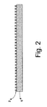
- Patterning of metals has been recently proposed to achieve an efficient TE (Myung-Gyu Kang and L. Jay Guo, "Nanoimprinted semitransparent metal electrodes and their application in organic light emitting diodes" Adv. Mater. 19, 1391-1396, 2007). The semitransparent metal electrodes are in the form of a nm-scale periodically perforated dense metal on the substrate (
Fig.2 ). By changing the aperture ratio and the thickness of the metal the optical transparency and the sheet resistance can be tuned. In fact it is shown that values comparable to ITO can be achieved at the same time for both parameters. The linewidth (i.e. the width of the regions where the metal is present) has to be sub-wavelength, to provide sufficient transparency and to minimize scattering. In addition the period of the structure has to be sub-micrometer to ensure the uniformity of the current onto the substrate surface (e.g. uniform injection or extraction of currents into or from an active layer). The latter drawback, i.e. the need of very small structural features with sub-micrometer periods, is due to the fact that the electrode is missing on the majority of the area and the ohmic loss due to conduction has to be kept small. The structure being in the nanometer to micron range, the proposed approach requires demanding and expensive conventional lithographic techniques for patterning. To make it less expensive nonconventional lithographic techniques, such as nano-imprinting, have been used (WO 2006/132672 A2 ). Such techniques have however several drawbacks, including likehood of missing metal lines and are more expensive than conventional techniques for patterning on a larger scale (micron to mm range), including UV lithography, screen printing and shadow masking during deposition. - Accordingly, it is aim of the present invention to devise a way to decrease the Rs value of UTMF based TE without significantly reducing the corresponding optical transmission. Therefore, the invention provides a transparent electrode comprising an ultra thin metal conductor with a thickness between 1 nm and 10nm, and further comprising a metal grid in contact with the ultra thin metal conductor, the metal grid comprising openings.
- The ultra thin metal conductor has preferably a thickness of 2nm to 8nm. Both the ultra thin metal and the grid can comprise Ni, Cr, Ti, Al, Cu, Ag , Au or a mixture thereof, being of the same or a different material. Preferably, the fill factor of the metal grid is not more than a 5% and the ultra thin metal conductor is continuous. The metal grid can have a thickness in the order of 10-9 m to 10-5 m and a linewidth between 5x10⁻⁶ m and 5x10⁻⁵ m. Optionally, the grid has a square or rectangular like pattern.
- The method of manufacturing the transparent electrode metal film comprises the steps of:
- a. depositing a continuous ultra thin metal film (2) on a substrate (1) with a thickness between 1 nm and 10nm
- b. depositing a metal grid comprising openings (3) on said continuous ultra thin metal film.
- Step a. is advantageously performed by sputtering deposition. Step b. can be performed by UV lithography, soft lithography, screen printing or by a shadow mask. The substrate comprises preferably silica, borosilicate, silicon, lithium niobate, or polyethylene terephthalate. The starting roughness of the substrate should be below the thickness of the film to assure its continuity. The metal conductor can be oxidized before or after the deposition of the grid.
- To complete the description and in order to provide for a better understanding of the invention, a set of drawings is provided. Said drawings form an integral part of the description and illustrate a preferred embodiment of the invention, which should not be interpreted as restricting the scope of the invention, but just as an example of how the invention can be embodied. The drawings comprise the following figures:
-
Fig. 1 shows the typical layout of a TE based on UTMF on a substrate according to the prior art -
Fig. 2 shows a nanoimprinted metal grid according to the prior art. -
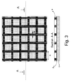
Fig. 3 shows a TE structure according to the invention composed of a uniform UTMF with a top metal grid. -
Fig. 4 shows the total sheet resistance (UTMF with top grid of structure infig. 3 ) as a function of grid linewidth (w) for different thickness. -
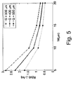
Fig. 5 shows the total sheet resistance (UTMF with top grid of structure infig. 4 ) as a function of grid linewidth (w) for different gaps, G=Λ-w, where Λ is the period. -
Fig. 6 shows the overall optical transmission with respect to the UTMF transmission (i.e. transmission decrease due to the grid) as a function of grid linewidth (w) for different gaps G=Λ-w. In practice for Ni, for example, the grid becomes opaque at tG≥40nm. - One aspect of the invention relies on the use of a uniform, continuous UTMF with a larger thickness metal grid on top of it (
Fig. 3 ). Depending on the application such grid can be either on a nm to micron scale (e.g. in the case of LEDs where the scattering due to metal lines are to be avoided to preserve the output optical beam quality) or micron to hundreds of microns scale (e.g. in the case of solar cells where preserving the quality of the incoming optical beam is not essential). The period and linewidth of the grid depend also on the thickness of the underneath UTMF and the local currents involved. In general the lower the UTMF thickness and the larger the current densities, the smaller the uncovered regions by the grid. The thickness of the metal grid (tG) is related to the fill factor (ratio between linewidth w and period Λ) and the thickness of the underneath UTMF (tUTMF). Note that the ρ values for the metal grid structure (ρG) are typically significantly lower than those of the UTMF layer (ρUTMF) because the larger the thickness of the metal layer (t) the lower the ρ value. This makes the sheet resistance Rs (=p/t) of the grid with respect to that of the UTMF underneath even lower than one would expect by simply scaling the thickness. In practical cases the sheet resistance of the underneath UTMF becomes negligible on a scale larger than the period of the grid, however still important locally (within the period length of the grid) to collect or inject charges from and into regions where the metal grid lines are absent. - One aspect of the present invention refers to a method to produce a metal based TE that comprises the steps of:
- a) depositing of a continuous UTMF film on a substrate;
- b) depositing of a metal grid on the aforesaid UTMF; to obtain a metal film which has a significantly reduced electrical sheet resistance and only slightly reduced optical transmission with respect to the initially deposited UTMF.
- The overall sheet resistance of the film structure reported in
fig. 3 (square mesh) can be written as
where all the parameters have already been defined above. In fact with good approximation the sheet resistance on a scale larger than the period of the mesh can be approximated by (ρ G/tG)(Λ/w), i.e. the sheet resistance of the top grid, being the sheet resistance of the UTMF much larger. However as it was said above the sheet resistance locally, within the inner square of linear dimension Λ-w, is given by the UTMF layer. - The overall optical transmission (T) is given by the following expression:

- Where TUTMF is the transmission of the initially deposited UTMF. Note that for simplicity we have assumed that the thickness of the metal grid is large enough to make it opaque.
- The above expressions hold for a square like mesh depicted in
fig. 3 , however the design guidelines illustrated for this pattern geometry apply also to any type of grids with continuous lines, e.g. rectangular or stripes. -
Fig. 4 ,5 and6 show the dependence of overall sheet resistance and optical transmission with respect to UTMF and grid parameters. The following parameters were assumed: Λ-w = 500 µm ; tUTMF = 2 nm ; ρG = 14 * 10 -9 Ωm ; ρUTMF = 191.2 * 10 -8 Ωm; tG = 500 nm. The ρ values are experimental values for Ni, in particular it was experimentally assessed that in practice the above ρG value holds for tG≥40nm. Above this tG, the grid becomes opaque. However the design principle of this invention applies to whatever metals, including structures where the UTMF and the grid are of different metals. From the figures it is clear that there exists a trade-off between sheet resistance and optical transmission. One can also straightforwardly appreciate that an appropriate Ni based grid allows achieving overall sheet resistance values well below 10 Ω/ without significant reduction in optical transmission, especially by increasing the grid thickness. - The above expressions with examples given in the micron range for the linewidth and period of the grid are still valid in the nm and hundreds of micrometers range and, as already said, can be adapted to any metal, combination of metals and grid geometry. Thus the design guidelines provided in this patent application can be generalised depending on device requirements (e.g. nm to micron or micron to hundreds of micron grid), fabrication constraints, etc. In particular the UTMF layer might be a different material than that of the metal grid. The former layer has to be transparent, sufficiently conductive within the uncovered regions by the grid, compatible with the substrate material (e.g. an appropriate work function in the case of active device) while the latter has mainly to be electrically efficient. Examples of metals for the UTMF and grid layers include Ni, Cr, Ti, Al, Cu, Ag and Au. A preliminary experimental assessment has been carried out using Ni UTMF and Ni grid. The following table summarises the obtained results.
ρ(µΩ.cm) Rs, TOT (Ω/ ) Optical transmission including substrate (%) Only Ni UTMF with tUTMF=2 mn 191.2 955 74.5 Ni UTMF above + Ni grid with w=5µm,G=500µm, tG=40nm - 350 72 Ni UTMF above + Ni grid with w=10µm,G=500µm, tG=40nm - 165 70.3 - The effect of reduction of sheet resistance and nearly unchanged optical transmission due to the grid is clearly evident, so is the dependence of both parameters with respect to linewidth of the grid. The experimental values of grid thickness were limited to 40 nm. It is however evident from
fig. 5 that larger grid thicknesses can be achieved to further reduce the overall sheet resistance, especially for grid structures with period and linewidth in the micron to hundreds of micron range. - Step a) of the process of the invention may be carried out according to any conventional method. In a particular embodiment, step a) is carried out by sputtering deposition under vacuum. The starting surface roughness of the substrate should preferably be below the thickness of the film; otherwise said film could be discontinuous and thus non-conductive.
- Generally the ultra thin metal film deposited in step a) presents a thickness comprised between 1 and 10 nm.
- Any metal may be used as the thin metal film as long as it maintains sufficient uniformity over the whole deposited area, especially for small thicknesses. In a particular embodiment Ni is used for both the UTMF and grid layers.
- The thin layer is deposited on to a substrate said substrate being a dielectric substrate, such as glass, a semiconductor, an inorganic crystal or plastic material. Examples of them are silica (SiO2), borosilicate (BK7), silicon (Si), lithium niobate (LiNbO3), or polyethylene terephthalate (PRT), among others, suitable for putting the invention into practice. Note that substrate refers to the material over which the UTMF is deposited. It can be part of a device structure, e.g. an active semiconductor or organic layer.
- Step b) of the method of the invention can be carried out in several ways, depending on the metal and dimensions of the structure. The grid patterning may rely , e.g., on UV lithography, soft lithography (nano-imprinting), screen printing or shadow mask, depending on the geometrical constraints, while the deposition on techniques similar to those used for the UTMF layer or others for thicker layers, e.g. evaporation or electroplating. All the techniques are known to a person skilled in the art.
- The sheet resistance of the initial UTMF should be in the 50 to 1000 Ω/ range, depending on the application and subsequent grid geometry while the decrease in optical transmission with respect to the substrate should be lower than 30% and preferably less than 10%. As a result of the subsequent grid fabrication the resulting overall sheet resistance should be in the range of 1 to 100 Ω/ while the optical transmission decrease should be in the range of 1 to 10%.
- Optionally the UTMF can be oxidised to increase its stability before or after the grid deposition.
- In view of the above it can be seen that the method of the present invention presents the important advantage of providing metal based TE with low sheet resistance which find many applications due to their simple and low cost method of fabrication and their intrinsic technical characteristics. In this sense it is known that in devices such as photovoltaic cells, organic light emitting diodes, displays, integrated electro-optic modulators, lasers and photo-detectors, transparent conductive electrodes are key elements, and are combined with other materials.
- The foregoing is illustrative of the present invention. This invention however is not limited to the following precise embodiment described herein, but encompasses all equivalent modifications within the scope of the claims which follow.
- A 2 nm ultrathin Ni film was deposited on a double side polished UV fused silica substrate using
Ajaint Orion 3 DC sputtering system. The sputtering was performed at room temperature in a pure argon atmosphere of 0.27 Pa (about 2 mTorr) and 100 W DC power. Prior to the deposition the substrate was cleaned with oxygen plasma with oxygen base pressure of 1.1 Pa (about 8 mTorr) and 40 W RF power for 15 minutes. - A positive photoresist is then spincoated on the film with 4000 rounds per minute and dwell time of 30 seconds. This recipe produces a photoresist thin film of about 1.2 - 1.3 µm. In fact, the thickness of the photoresist determines the maximum thickness of the metal grid to be deposited later in the process. The sample is then baked at 90 C for 5 minutes to evaporate the solvent in the photoresist. Thereafter, the sample is exposed to UV light for 15 seconds using Quintal Q4000 mask aligner with a hard mask of desired grid pattern placed on top of the sample. The exposed sample is then developed for about 40 seconds which removes the photoresist in the regions of the sample where the UV light is not blocked by the hard mask, thus making openings in the sample to deposit the thick metal grid.
- The sample is again loaded in the sputtering chamber and a thick metal is deposited using the same aforementioned conditions. After depositing the thick metal the sample is dipped in acetone and placed in an ultrasonic bath till the remaining photoresist is lifted off.
- The sheet resistance of the obtained structure (UTMF together with grid) as well as the initial UTMF film is measured by Cascade Microtech 44/7S Four point Probe and Keithley 2001 multimeter. For the transmission spectra, a Perkin Elmer Lambda 950 spectrophotometer was used.
- In this text, the term "comprises" and its derivations (such as "comprising", etc.) should not be understood in an excluding sense, that is, these terms should not be interpreted as excluding the possibility that what is described and defined may include further elements, steps, etc.
- On the other hand, the invention is obviously not limited to the specific embodiment(s) described herein, but also encompasses any variations that may be considered by any person skilled in the art (for example, as regards the choice of materials, dimensions, components, configuration, etc.), within the general scope of the invention as defined in the claims.
Claims (15)
- Transparent electrode comprising an ultra thin metal conductor (2) with a thickness between 1 nm and 10nm characterized in that it further comprises a metal grid in contact with the ultra thin metal conductor (3), the metal grid comprising openings.
- Transparent electrode according to claim 1 wherein the ultra thin metal conductor has a thickness of 2nm to 8nm.
- Transparent electrode according to any of the preceding claims wherein the ultra thin metal conductor comprises Ni, Cr, Ti, Al, Cu, Ag , Au or a mixture thereof.
- Transparent electrode according to any of the preceding claims wherein the metal grid comprises Ni, Cr, Ti, Al, Cu, Ag , Au or a mixture thereof.
- Transparent electrode according to any of the preceding claims, wherein the fill factor of the metal grid is not more than a 5%.
- Transparent electrode according to any of the preceding claims wherein the ultra thin metal conductor is continuous.
- Transparent electrode according to any of the preceding claims wherein the metal grid has a thickness in the order of 10-9 m to 10-5 m.
- Transparent electrode according to any of the preceding claims wherein the metal grid has a linewidth between 5x10⁻⁶ m and 5x10⁻⁵ m.
- Transparent electrode according to any of the previous claims wherein the metal grid has a square or rectangular like pattern.
- Method of manufacturing a transparent electrode comprising the steps:a. depositing a continuous ultra thin metal film (2) on a substrate (1) with a thickness between 1 nm and 10nmb. depositing a metal grid comprising openings (3) on said continuous ultra thin metal film
- Method according to claim 10 wherein step a. is performed by sputtering deposition.
- Method according to any of the claims 10-11 wherein step b. is performed by UV lithography, soft lithography, screen printing or by a shadow mask.
- Method according to any of the claims 10-12 wherein the substrate comprises silica, borosilicate, silicon, lithium niobate, or polyethylene terephthalate.
- Method according to any of claims 10-13 wherein the starting roughness of the substrate is below the thickness of the film.
- Method according to any of claims 10-14 wherein the ultra thin metal conductor is oxidized before or after the deposition of the grid.
Priority Applications (3)
| Application Number | Priority Date | Filing Date | Title |
|---|---|---|---|
| EP09382079A EP2259329A1 (en) | 2009-05-26 | 2009-05-26 | Metal transparent conductors with low sheet resistance |
| US13/322,810 US20120103669A1 (en) | 2009-05-26 | 2010-05-21 | Metal transparent conductors with low sheet resistance |
| PCT/EP2010/057026 WO2010136393A2 (en) | 2009-05-26 | 2010-05-21 | Metal transparent conductors with low sheet resistance |
Applications Claiming Priority (1)
| Application Number | Priority Date | Filing Date | Title |
|---|---|---|---|
| EP09382079A EP2259329A1 (en) | 2009-05-26 | 2009-05-26 | Metal transparent conductors with low sheet resistance |
Publications (1)
| Publication Number | Publication Date |
|---|---|
| EP2259329A1 true EP2259329A1 (en) | 2010-12-08 |
Family
ID=41172332
Family Applications (1)
| Application Number | Title | Priority Date | Filing Date |
|---|---|---|---|
| EP09382079A Ceased EP2259329A1 (en) | 2009-05-26 | 2009-05-26 | Metal transparent conductors with low sheet resistance |
Country Status (3)
| Country | Link |
|---|---|
| US (1) | US20120103669A1 (en) |
| EP (1) | EP2259329A1 (en) |
| WO (1) | WO2010136393A2 (en) |
Cited By (3)
| Publication number | Priority date | Publication date | Assignee | Title |
|---|---|---|---|---|
| WO2013113638A1 (en) * | 2012-01-30 | 2013-08-08 | Ewe-Forschungszentrum Für Energietechnologie E. V. | Photovoltaic solar cell and method for producing a photovoltaic solar cell |
| US10355149B2 (en) | 2016-06-17 | 2019-07-16 | Industrial Technology Research Institute | Tandem solar cell module |
| CN119815936A (en) * | 2025-03-12 | 2025-04-11 | 浙江爱旭太阳能科技有限公司 | A solar cell, a battery assembly and a photovoltaic system |
Families Citing this family (16)
| Publication number | Priority date | Publication date | Assignee | Title |
|---|---|---|---|---|
| US20120018770A1 (en) * | 2010-07-23 | 2012-01-26 | Min-Hao Michael Lu | Oled light source having improved total light emission |
| EP2603936B1 (en) * | 2010-08-10 | 2016-05-11 | Koninklijke Philips N.V. | Shunting layer arrangement for leds |
| TWI543199B (en) * | 2010-11-02 | 2016-07-21 | 坎畢歐科技公司 | Grid-like and nano-structured transparent conductor for low sheet resistance application and method of forming same |
| US20120267658A1 (en) * | 2011-04-20 | 2012-10-25 | Invenlux Limited | Large-area light-emitting device and method for fabricating the same |
| WO2013123066A1 (en) * | 2012-02-14 | 2013-08-22 | Bandgap Engineering, Inc. | Screen printing electrical contacts to nanowire areas |
| CN103579380A (en) * | 2012-08-09 | 2014-02-12 | 索尼公司 | Light-receiving or light-emitting component, solar cell, optical sensor and LED |
| US9066425B2 (en) | 2013-04-01 | 2015-06-23 | Rohm And Haas Electronic Materials Llc | Method of manufacturing a patterned transparent conductor |
| WO2015148637A1 (en) * | 2014-03-25 | 2015-10-01 | Tel Solar Ag | Thin film solar cells with metallic grid contacts |
| CN105070771A (en) * | 2015-08-06 | 2015-11-18 | 南昌大学 | Metal electrode for light inlet surface of crystalline silicon heterojunction solar cell and preparation method of metal electrode |
| US9801284B2 (en) | 2015-11-18 | 2017-10-24 | Dow Global Technologies Llc | Method of manufacturing a patterned conductor |
| US10228495B2 (en) * | 2016-09-08 | 2019-03-12 | Goodrich Corporation | Apparatus and methods of electrically conductive optical semiconductor coating |
| CN109935839B (en) * | 2017-12-19 | 2024-04-02 | 成都大超科技有限公司 | Current collector, lithium battery cell and lithium battery |
| US11745702B2 (en) * | 2018-12-11 | 2023-09-05 | Ppg Industries Ohio, Inc. | Coating including electrically conductive lines directly on electrically conductive layer |
| JP2021163793A (en) * | 2020-03-30 | 2021-10-11 | 日東電工株式会社 | Impedance matching film and electromagnetic wave absorber |
| JP2021164011A (en) * | 2020-03-30 | 2021-10-11 | 日東電工株式会社 | Impedance matching film and electromagnetic wave absorber |
| JP2022152689A (en) * | 2021-03-29 | 2022-10-12 | 株式会社ジャパンディスプレイ | flexible substrate |
Citations (5)
| Publication number | Priority date | Publication date | Assignee | Title |
|---|---|---|---|---|
| US4345107A (en) * | 1979-06-18 | 1982-08-17 | Ametek, Inc. | Cadmium telluride photovoltaic cells |
| EP1453117A2 (en) * | 2003-02-26 | 2004-09-01 | Schott Glas | Method for fabricating organic light emitting diodes and organic light emitting diode |
| JP2006134827A (en) * | 2004-11-09 | 2006-05-25 | Nippon Oil Corp | Electrode and dye-sensitized solar cell |
| WO2006132672A2 (en) | 2005-06-02 | 2006-12-14 | Dow Corning Corporation | A method of nanopatterning, a cured resist film use therein, and an article including the resist film |
| EP2031660A2 (en) * | 2007-08-29 | 2009-03-04 | The Boeing Company | Photovoltaic cells with selectively patterned transparent conductive coatings, and associated methods |
Family Cites Families (4)
| Publication number | Priority date | Publication date | Assignee | Title |
|---|---|---|---|---|
| TWI234885B (en) * | 2002-03-26 | 2005-06-21 | Fujikura Ltd | Electroconductive glass and photovoltaic cell using the same |
| EP2071633A4 (en) * | 2006-08-31 | 2011-03-16 | Nat Inst Of Advanced Ind Scien | TRANSPARENT ELECTRODE SUBSTRATE FOR SOLAR CELL |
| WO2009008323A1 (en) * | 2007-07-09 | 2009-01-15 | Japan Science And Technology Agency | Photoelectric converter and solar cell using the same |
| US20090211627A1 (en) * | 2008-02-25 | 2009-08-27 | Suniva, Inc. | Solar cell having crystalline silicon p-n homojunction and amorphous silicon heterojunctions for surface passivation |
-
2009
- 2009-05-26 EP EP09382079A patent/EP2259329A1/en not_active Ceased
-
2010
- 2010-05-21 WO PCT/EP2010/057026 patent/WO2010136393A2/en not_active Ceased
- 2010-05-21 US US13/322,810 patent/US20120103669A1/en not_active Abandoned
Patent Citations (5)
| Publication number | Priority date | Publication date | Assignee | Title |
|---|---|---|---|---|
| US4345107A (en) * | 1979-06-18 | 1982-08-17 | Ametek, Inc. | Cadmium telluride photovoltaic cells |
| EP1453117A2 (en) * | 2003-02-26 | 2004-09-01 | Schott Glas | Method for fabricating organic light emitting diodes and organic light emitting diode |
| JP2006134827A (en) * | 2004-11-09 | 2006-05-25 | Nippon Oil Corp | Electrode and dye-sensitized solar cell |
| WO2006132672A2 (en) | 2005-06-02 | 2006-12-14 | Dow Corning Corporation | A method of nanopatterning, a cured resist film use therein, and an article including the resist film |
| EP2031660A2 (en) * | 2007-08-29 | 2009-03-04 | The Boeing Company | Photovoltaic cells with selectively patterned transparent conductive coatings, and associated methods |
Non-Patent Citations (6)
| Title |
|---|
| GOSH D S ET AL: "Widely transparent electrodes based on ultrathin metals", OPTICS LETTERS, OSA, OPTICAL SOCIETY OF AMERICA, WASHINGTON, DC, US, vol. 34, no. 3, 1 February 2009 (2009-02-01), pages 325 - 327, XP001521884, ISSN: 0146-9592 * |
| MYUNG-GYU KANG; L. JAY GUO: "Nanoimprinted semitransparent metal electrodes and their application in organic light emitting diodes", ADV. MATER., vol. 19, 2007, pages 1391 - 1396, XP055136367, DOI: doi:10.1002/adma.200700134 |
| R. B. PODE: "Transparent conducting metal electrode for top emission organic light-emitting devices: Ca-Ag double layer", APPL. PHYS. LETT., vol. 84, 2004, pages 4614, XP012061680, DOI: doi:10.1063/1.1756674 |
| S. GIURGOLA ET AL.: "Ultra thin nickel transparent electrodes", J. MATER. SCI: MATER. ELECTRON., vol. 20, 2009, pages S181 - S184 |
| S. GIURGOLA; P. VERGANI; V. PRUNERI: "Ultra thin metal films as an alternative to TCOs for optoelectronic applications", NUOVO CIMENTO B, vol. 121, 2006, pages 887 - 897 |
| SABRINA CONOCI ET AL.: "Optically Transparent, Ultrathin Pt Films as Versatile Metal Substrates for Molecular Optoelectronics", ADVANCED FUNCTIONAL MATERIALS, vol. 16, no. 11, pages 1425 - 1432, XP001243742, DOI: doi:10.1002/adfm.200500893 |
Cited By (3)
| Publication number | Priority date | Publication date | Assignee | Title |
|---|---|---|---|---|
| WO2013113638A1 (en) * | 2012-01-30 | 2013-08-08 | Ewe-Forschungszentrum Für Energietechnologie E. V. | Photovoltaic solar cell and method for producing a photovoltaic solar cell |
| US10355149B2 (en) | 2016-06-17 | 2019-07-16 | Industrial Technology Research Institute | Tandem solar cell module |
| CN119815936A (en) * | 2025-03-12 | 2025-04-11 | 浙江爱旭太阳能科技有限公司 | A solar cell, a battery assembly and a photovoltaic system |
Also Published As
| Publication number | Publication date |
|---|---|
| WO2010136393A2 (en) | 2010-12-02 |
| WO2010136393A3 (en) | 2011-02-17 |
| US20120103669A1 (en) | 2012-05-03 |
Similar Documents
| Publication | Publication Date | Title |
|---|---|---|
| US20120103669A1 (en) | Metal transparent conductors with low sheet resistance | |
| EP2317562A1 (en) | Multilayer metallic electrodes for optoelectronics | |
| KR101680928B1 (en) | Transparent electrode based on combination of transparent conductive oxides, metals and oxides | |
| US9253890B2 (en) | Patterned conductive film, method of fabricating the same, and application thereof | |
| CN102779944B (en) | Transparent conductive thin film | |
| KR101621571B1 (en) | Method to prepare a stable transparent electrode | |
| KR101682501B1 (en) | Transparant electrode containing silver nanowire-patterned layer and graphene layer, and manufacturing method thereof | |
| EP1839347A2 (en) | Electro-optical element comprising a controlled, in particular, uniform functionality distribution | |
| CN102365765B (en) | Schottky type junction device, the electrooptical device using it and solaode | |
| Kim et al. | Embedded oxidized Ag–Pd–Cu ultrathin metal alloy film prepared at low temperature with excellent electronic, optical, and mechanical properties | |
| Chang et al. | Characteristics of high-power impulse magnetron sputtering ITO/Ag/ITO films for application in transparent micro-LED displays | |
| KR20140133317A (en) | Transparent conductor comprising silver nanowire and silver grid complex pattern and method of manufacturing the same | |
| KR101955671B1 (en) | Patterning Method for Graphene or Graphene-Metal Hybrid Films | |
| CN107275007B (en) | A kind of compound transparent electricity conductive film and preparation method thereof | |
| CN117015833B (en) | Flexible transparent electrodes of silver nanowires sintered with metal oxide nanoparticles | |
| Koiry et al. | An electrochemical method for fast and controlled etching of fluorine-doped tin oxide coated glass substrates | |
| Witczak et al. | Flexible quantum-dot light-emitting diodes using embedded silver mesh transparent electrodes manufactured by an ultraprecise deposition method | |
| EP2851967B1 (en) | Method for forming transparent electrode and semiconductor device manufactured using same | |
| CN107359212A (en) | Electrically conducting transparent substrate, its preparation method and solar cell | |
| JP5018951B2 (en) | electrode | |
| JP4742584B2 (en) | electrode | |
| JP3837471B2 (en) | Modified electrode and electrode modification method | |
| KR101420289B1 (en) | Semiconductor device and method for manufacturing the same | |
| KR102519888B1 (en) | Methode of manufacturing low resistrance transparent electrode having metal mesh | |
| Tan et al. | ZrAlOX‐PVP Hybrid Dielectric Enables High‐Performance Phototransistors for Full‐Spectral Response and Full‐Color Quantum‐Dot Light‐Emitting Diodes |
Legal Events
| Date | Code | Title | Description |
|---|---|---|---|
| PUAI | Public reference made under article 153(3) epc to a published international application that has entered the european phase |
Free format text: ORIGINAL CODE: 0009012 |
|
| AK | Designated contracting states |
Kind code of ref document: A1 Designated state(s): AT BE BG CH CY CZ DE DK EE ES FI FR GB GR HR HU IE IS IT LI LT LU LV MC MK MT NL NO PL PT RO SE SI SK TR |
|
| 17P | Request for examination filed |
Effective date: 20110606 |
|
| 17Q | First examination report despatched |
Effective date: 20120220 |
|
| RAP1 | Party data changed (applicant data changed or rights of an application transferred) |
Owner name: FUNDACIO INSTITUT DE CIENCIES FOTONIQUES Owner name: INSTITUCIO CATALANA DE RECERCA I ESTUDIS AVANCATS |
|
| RIN1 | Information on inventor provided before grant (corrected) |
Inventor name: PRUNERI, VALERIO Inventor name: GHOSH, DHRITI, SUNDAR |
|
| STAA | Information on the status of an ep patent application or granted ep patent |
Free format text: STATUS: THE APPLICATION HAS BEEN REFUSED |
|
| 18R | Application refused |
Effective date: 20180921 |