EP2259018A1 - Gap control for die or layer bonding using intermediate layers - Google Patents
Gap control for die or layer bonding using intermediate layers Download PDFInfo
- Publication number
- EP2259018A1 EP2259018A1 EP09161583A EP09161583A EP2259018A1 EP 2259018 A1 EP2259018 A1 EP 2259018A1 EP 09161583 A EP09161583 A EP 09161583A EP 09161583 A EP09161583 A EP 09161583A EP 2259018 A1 EP2259018 A1 EP 2259018A1
- Authority
- EP
- European Patent Office
- Prior art keywords
- layer
- groove
- gap
- recess
- sealing material
- Prior art date
- Legal status (The legal status is an assumption and is not a legal conclusion. Google has not performed a legal analysis and makes no representation as to the accuracy of the status listed.)
- Granted
Links
Images




Classifications
-
- G—PHYSICS
- G01—MEASURING; TESTING
- G01C—MEASURING DISTANCES, LEVELS OR BEARINGS; SURVEYING; NAVIGATION; GYROSCOPIC INSTRUMENTS; PHOTOGRAMMETRY OR VIDEOGRAMMETRY
- G01C19/00—Gyroscopes; Turn-sensitive devices using vibrating masses; Turn-sensitive devices without moving masses; Measuring angular rate using gyroscopic effects
- G01C19/56—Turn-sensitive devices using vibrating masses, e.g. vibratory angular rate sensors based on Coriolis forces
-
- B—PERFORMING OPERATIONS; TRANSPORTING
- B81—MICROSTRUCTURAL TECHNOLOGY
- B81C—PROCESSES OR APPARATUS SPECIALLY ADAPTED FOR THE MANUFACTURE OR TREATMENT OF MICROSTRUCTURAL DEVICES OR SYSTEMS
- B81C1/00—Manufacture or treatment of devices or systems in or on a substrate
- B81C1/00015—Manufacture or treatment of devices or systems in or on a substrate for manufacturing microsystems
- B81C1/00261—Processes for packaging MEMS devices
- B81C1/00269—Bonding of solid lids or wafers to the substrate
-
- G—PHYSICS
- G01—MEASURING; TESTING
- G01P—MEASURING LINEAR OR ANGULAR SPEED, ACCELERATION, DECELERATION, OR SHOCK; INDICATING PRESENCE, ABSENCE, OR DIRECTION, OF MOVEMENT
- G01P15/00—Measuring acceleration; Measuring deceleration; Measuring shock, i.e. sudden change of acceleration
- G01P15/02—Measuring acceleration; Measuring deceleration; Measuring shock, i.e. sudden change of acceleration by making use of inertia forces using solid seismic masses
- G01P15/08—Measuring acceleration; Measuring deceleration; Measuring shock, i.e. sudden change of acceleration by making use of inertia forces using solid seismic masses with conversion into electric or magnetic values
- G01P15/0802—Details
-
- G—PHYSICS
- G01—MEASURING; TESTING
- G01P—MEASURING LINEAR OR ANGULAR SPEED, ACCELERATION, DECELERATION, OR SHOCK; INDICATING PRESENCE, ABSENCE, OR DIRECTION, OF MOVEMENT
- G01P15/00—Measuring acceleration; Measuring deceleration; Measuring shock, i.e. sudden change of acceleration
- G01P15/02—Measuring acceleration; Measuring deceleration; Measuring shock, i.e. sudden change of acceleration by making use of inertia forces using solid seismic masses
- G01P15/08—Measuring acceleration; Measuring deceleration; Measuring shock, i.e. sudden change of acceleration by making use of inertia forces using solid seismic masses with conversion into electric or magnetic values
- G01P15/125—Measuring acceleration; Measuring deceleration; Measuring shock, i.e. sudden change of acceleration by making use of inertia forces using solid seismic masses with conversion into electric or magnetic values by capacitive pick-up
-
- H—ELECTRICITY
- H10—SEMICONDUCTOR DEVICES; ELECTRIC SOLID-STATE DEVICES NOT OTHERWISE PROVIDED FOR
- H10W—GENERIC PACKAGES, INTERCONNECTIONS, CONNECTORS OR OTHER CONSTRUCTIONAL DETAILS OF DEVICES COVERED BY CLASS H10
- H10W76/00—Containers; Fillings or auxiliary members therefor; Seals
- H10W76/60—Seals
-
- B—PERFORMING OPERATIONS; TRANSPORTING
- B81—MICROSTRUCTURAL TECHNOLOGY
- B81B—MICROSTRUCTURAL DEVICES OR SYSTEMS, e.g. MICROMECHANICAL DEVICES
- B81B2201/00—Specific applications of microelectromechanical systems
- B81B2201/02—Sensors
- B81B2201/0228—Inertial sensors
- B81B2201/0235—Accelerometers
-
- B—PERFORMING OPERATIONS; TRANSPORTING
- B81—MICROSTRUCTURAL TECHNOLOGY
- B81B—MICROSTRUCTURAL DEVICES OR SYSTEMS, e.g. MICROMECHANICAL DEVICES
- B81B2201/00—Specific applications of microelectromechanical systems
- B81B2201/02—Sensors
- B81B2201/0228—Inertial sensors
- B81B2201/0242—Gyroscopes
-
- G—PHYSICS
- G01—MEASURING; TESTING
- G01P—MEASURING LINEAR OR ANGULAR SPEED, ACCELERATION, DECELERATION, OR SHOCK; INDICATING PRESENCE, ABSENCE, OR DIRECTION, OF MOVEMENT
- G01P15/00—Measuring acceleration; Measuring deceleration; Measuring shock, i.e. sudden change of acceleration
- G01P15/02—Measuring acceleration; Measuring deceleration; Measuring shock, i.e. sudden change of acceleration by making use of inertia forces using solid seismic masses
- G01P15/08—Measuring acceleration; Measuring deceleration; Measuring shock, i.e. sudden change of acceleration by making use of inertia forces using solid seismic masses with conversion into electric or magnetic values
- G01P2015/0805—Measuring acceleration; Measuring deceleration; Measuring shock, i.e. sudden change of acceleration by making use of inertia forces using solid seismic masses with conversion into electric or magnetic values being provided with a particular type of spring-mass-system for defining the displacement of a seismic mass due to an external acceleration
- G01P2015/0822—Measuring acceleration; Measuring deceleration; Measuring shock, i.e. sudden change of acceleration by making use of inertia forces using solid seismic masses with conversion into electric or magnetic values being provided with a particular type of spring-mass-system for defining the displacement of a seismic mass due to an external acceleration for defining out-of-plane movement of the mass
- G01P2015/0825—Measuring acceleration; Measuring deceleration; Measuring shock, i.e. sudden change of acceleration by making use of inertia forces using solid seismic masses with conversion into electric or magnetic values being provided with a particular type of spring-mass-system for defining the displacement of a seismic mass due to an external acceleration for defining out-of-plane movement of the mass for one single degree of freedom of movement of the mass
- G01P2015/0828—Measuring acceleration; Measuring deceleration; Measuring shock, i.e. sudden change of acceleration by making use of inertia forces using solid seismic masses with conversion into electric or magnetic values being provided with a particular type of spring-mass-system for defining the displacement of a seismic mass due to an external acceleration for defining out-of-plane movement of the mass for one single degree of freedom of movement of the mass the mass being of the paddle type being suspended at one of its longitudinal ends
Definitions
- the present invention relates to ways of accurately controlling the dimensions of a gap provided between two layers of a structure being joined together.
- Micro-electromechanical systems such as accelerometers or gyros, often require a gap to be provided between a portion of two layers. This gap may be required, for example, for capacitive functions in a moving structure of the device, self-test excitation or damping of a moving structure.
- the gap In such systems, extremely accurate control of the gap dimensions is required, often down to micron level. Furthermore, the gap often needs to be hermetically sealed, generally in a controlled atmosphere, a gas filled environment or a vacuum.
- TSV through-silicon-vias
- An existing method of creating a gap between two layers being joined together is based on anodic bonding.
- a problem with this technique is that the bond members must be of different materials with non-matching mechanical or temperature characteristics, in addition to requiring a high electric field during processing.
- Other methods of bonding include adhesive bonding, glass frit bonding, direct/fusion bonding and eutectic (e.g. AuSn) bonding.
- AuSn eutectic
- a structure having a gap provided between a portion of two layers that are joined together comprising:
- a method of accurately controlling the dimensions of a gap provided between a portion of two layers joined together comprising the steps of:
- the first layer 11 comprises an element 10, for example an accelerometer.
- the second layer 12 comprises a recess 15 provided on the surface that is to be bonded to the first layer 11.
- the element 10 is surrounded by a groove 14 which provides a boundary around the element 10 and recess 15.
- the groove 14 is, ideally, etched into the surface of the first layer 11.
- the groove 14 could, however, be provided in either, or indeed both, the surfaces of the first and second layers 11,12.
- first portion 13a of sealing material 13 for example metal sealant.
- a second portion 13b of sealing material 13 is provided on the surface of the second layer 12, surrounding the recess 15.
- the second portion 13b of sealing material 13 has, in this example, a similar thickness to the first portion 13a of sealing material 13 and is arranged to be aligned with the first portion 13a of sealing material 13 when the first and second layers 11, 12 are joined together, as shown in Figure 1A .
- the first and second portions 13a, 13b of sealing material 13 are brought into contact causing the sealing material 13 to deform laterally within the groove 14, thereby creating a seal around the element 10, as shown in Figure 1B .
- the seal is, preferably, a hermetic seal.
- first and second portions of sealing material are of similar thickness.
- first and second portions of sealing material may have different heights and widths, provided that their combined height is greater than the depth of the groove and their width is configured such that, when the first and second layers are bonded together, the sealing material is laterally deformed and, furthermore, entirely retained within the groove.
- the amount of sealing material provided should be sufficient to ensure that it deforms within the groove, this amount should not be so great that it cannot be entirely accommodated within the groove after the first and second layers have been bonded together. This ensures that the surfaces of the first and second layers are in direct contact, lying adjacent to and flat against one another, after bonding has taken place.
- the depth of the groove should be smaller than the overall, combined, thickness of the sealing material to ensure a proper squeeze of the sealing material during the sealing process, but wide enough to fully accommodate the lateral deformation of sealing material.
- sealing material need only be provided in the groove, or on the surface of the second layer, and not necessarily both, provided a sufficient amount of sealing material is provided to ensure that it is squeezed between the layers and hence deformed within the groove to form a seal when the first and second layers are bonded together, as explained above.
- the sealing material is not provided within the groove on one of the layers it should be arranged on the surface of the other layer such that when the first and second layers are bonded together it deforms within the groove.
- the recess 15 provides a gap 17 above the element 10. Since the recess 15 is formed in the second layer 12 before bonding takes place, and because the surfaces of the first and second layers 11, 12 are bonded flat against one another thanks to the sealing material 13 being completely contained within the groove 14, the known depth of the recess 15 in the second layer 12 is therefore the exact height of the gap 17 provided above the element 10 after bonding.
- Figures 2A and 2B show a second a further example of the present invention, which is essentially the same as the first example, with the exception that no recess is provided in the surface of the second layer 22. Instead, the gap 27 is created and its dimensions controlled by forming a recess 25 in the surface of the first layer 21 by positioning the element 20 a predetermined and precise amount below the surface of the first layer, thereby effectively providing a precisely dimensioned gap 27 between the element 20 and the surface of the second layer 22.
- a groove 24 containing deformed sealing material 13 provides a seal around the element 20. It will be appreciated, however, that although in this example the groove 24 is provided in the surface of the first layer, the groove could be provided in the surface of the second layer 22 to provide the same result.
- a groove 34a, 34b is provided in the surface of both the first and second layers 31, 32, with first and second portions of sealing material 33a, 33b provided in each of the grooves 34a, 34b, respectively.
- the sealing material 33 is deformedly retained in the grooves 34a, 34b, when the first and second layers are joined, to form a seal around the element 30.
- the recess 35 could be provided on the surface of either the first or second layer 31, 32 to form the gap 37 between the element 30 and the surface of the second layer 32.
- a recess could be provided in the surfaces of both the first and second layers and/or a groove could be provided on the surface of both layers, if desired.
- the invention can be performed by providing the groove or recess on either the first or second layer surfaces, or even both, if desired.
- FIG. 4A A fourth example of the present invention is shown in Figure 4A , which comprises a similar arrangement to the examples described above.
- This further example has the additional feature of a vertical through conductor 49, also sometimes called a through silicon via (TSV), provided in the second layer 42.
- TSV 49 provides an electrical connection between a contact 46, provided on an upper surface of the second layer 42, and the first layer 41, as follows.
- a first portion 48a of electrical connection material 48 for example gold or copper, is provided in the groove 44 that is formed in the surface of the first layer 41 and surrounds the element 40.
- the electrical interconnect material 48 can be arranged either on the element 40 side of the sealing material 43, or on the outer side of the sealing material 43.
- a corresponding second portion 48b of, ideally, the same, or a similar, electrical interconnect material 48 is arranged on a lower surface of the second layer 42.
- the TSV 45 is arranged to pass through the second layer 42 so that it connects the electrical contact 46 on the upper surface of the second layer 42 with the second portion 48b of electrical interconnect material 48 provided on the lower surface of the second layer 42.
- a TSV could alternatively, be arranged to pass through the first layer 41 or, indeed, both first and second layers 41, 42, if desired.
- sufficient electrical interconnect material 48 is provided so that when the first and second layers 41, 42 are bonded together an electrical connection is formed by the first and second portions 48a, 48b of electrical interconnect material 48 being squeezed together such that they deform within the groove 44 to form a secure electrical connection.
- the heights and widths of the electrical interconnect material can vary, provided that it is caused to deform within the groove when the first and second layers are bonded together.
- Figure 4B shows the first layer 41 and the second layer 42 joined together after bonding.
- the sealing material 43 in the groove 44 has been squeezed together and has subsequently deformed to provide a seal around the element 40.
- the electrical interconnect material 48 has also been squeezed together and deformed within the groove 44 to provide a secure electrical connection.
- the groove 44 must therefore be of an appropriate size to accommodate both the sealing material 43 and the electrical interconnect material 48 after deformation, such that the surfaces of the first layer 41 and the second layer 42 are in full contact after bonding has taken place.
- an electrical connection could be formed by the electrical interconnect material 48 being deformed within a separate groove portion (not shown).
- groove 44 may be fully covered by the second layer 42, as shown in the example of Figure 4B .
- sealing material 43 and/or, electrical interconnect material 48 could alternatively be provided only on the surface of one of the layers 41, 42, provided that the overall height of the material 43, 48 is greater than the depth of the groove 44 that it is intended to deform in such that when the layers 41, 42 are brought together it deforms within the groove 44.
- Figures 5A and 5B show a fifth example of the present invention that is substantially the same as the fourth example described above, with the exception that the groove 54 is provided in the surface of the second layer 52 and the recess 55 is provided in the surface of the first layer 51.
- sealing material 53 and electrical interconnect material 58 are only provided on the first layer. However, as outlined previously, sufficient amounts of sealing material 53 and electrical interconnect material 58 are provided to ensure that their respective heights are both greater than the depth of the groove 54. Thus, when the first and second layers 51, 52 are bonded together, the sealing material 53 and electrical interconnect material 58 are both deformedly retained within the groove 54, as can clearly be seen from Figure 5B .
- the TSV may be replaced by, for example, an electrode or a patterned structure/layer.
- Figures 6A and 6B show a sixth example of the present invention that is substantially the same as the fourth example, with the exception that the TSV has been replaced by an electrode 66 situated, in this example, in the recess 65 formed in the surface of the second layer 62.
- Figure 6B it can be seen how the first and second portions 68a, 68b of electrical interconnect material 68 are aligned such that, on bonding the first and second layers 61, 62 together, the first and second portions 68a, 68b of interconnect material 68 are squeezed together such that they are deformed, in the same manner as the first and second portions 63a, 63b of sealing material 63, in a portion of groove 64, to form an electrical connection between the first layer 61 and the electrode 66 provided on the surface of the second layer 62.
- the electrode could be substituted by a patterned structure or one or more component(s) suitable for sending and/or receiving an electrical signal.
- an advantage of the present invention is that the dimensions of a gap provided above an element can be accurately created and controlled independently of the sealing process between two layers.
- the present invention enables gap dimension control to be extremely accurate, even when providing a hermetic seal around an element when bonding two layers, because it is known that the surfaces of the layers will be in full surface contact with one another.
- the present invention eliminates the variable of the gap dimension, previously introduced by an inability to accurately control the thickness of sealing material between two bonded layers, when designing components requiring accurately controlled gap dimensions.
- the thickness of the seal can be controlled by the amount of sealing material provided, together with the depth and width of the groove without having any effect on the gap provided above the element.
Landscapes
- Engineering & Computer Science (AREA)
- Physics & Mathematics (AREA)
- General Physics & Mathematics (AREA)
- Microelectronics & Electronic Packaging (AREA)
- Manufacturing & Machinery (AREA)
- Radar, Positioning & Navigation (AREA)
- Remote Sensing (AREA)
- Micromachines (AREA)
Abstract
Description
- The present invention relates to ways of accurately controlling the dimensions of a gap provided between two layers of a structure being joined together.
- Micro-electromechanical systems (MEMS), such as accelerometers or gyros, often require a gap to be provided between a portion of two layers. This gap may be required, for example, for capacitive functions in a moving structure of the device, self-test excitation or damping of a moving structure.
- In such systems, extremely accurate control of the gap dimensions is required, often down to micron level. Furthermore, the gap often needs to be hermetically sealed, generally in a controlled atmosphere, a gas filled environment or a vacuum.
- This combined requirement has limited the bonding methods that are currently possible. Current metal bonds based on solders, eutectic or similar process approaches are of limited use because the required thickness of such layers and the metal float phase of the bonding process makes accurate gap control very difficult.
- Furthermore, in a number of applications, there is a need to provide an electrical connection between the main structure and, for example, electrodes or a patterned structure on the sealing part. There is also sometimes a need to provide one or more vertical electrical connections through the whole structure. These are sometimes called vertical through conductors, or through-silicon-vias (TSV).
- An existing method of creating a gap between two layers being joined together is based on anodic bonding. A problem with this technique, however, is that the bond members must be of different materials with non-matching mechanical or temperature characteristics, in addition to requiring a high electric field during processing. Other methods of bonding include adhesive bonding, glass frit bonding, direct/fusion bonding and eutectic (e.g. AuSn) bonding. However, although these methods are able to create seals, they are not able to provide very accurate gap control.
- According to the present invention there is provided a structure having a gap provided between a portion of two layers that are joined together, the structure comprising:
- a first layer having an element formed within a first surface;
- a second layer having a second surface, adjacent to and in direct contact with at least a portion of the first surface on all sides of the element such that the element is completely enclosed;
- a recess of predetermined depth arranged to provide the gap between the element and the second surface;
- a groove formed in one of the first surface or second surface, the groove defining a boundary around the element; and
- sealing material deformedly retained completely within the groove to form a seal around the element, such that the recess defines the gap.
- According to the present invention there is also provided a method of accurately controlling the dimensions of a gap provided between a portion of two layers joined together, the method comprising the steps of:
- providing a first layer with an element formed within a first surface;
- providing a second layer with a second surface;
- forming a recess in one of the first surface or second surface, the recess having a predetermined depth;
- forming a groove in one of the first surface or second surface, the groove defining a boundary for surrounding the element;
- providing sealing material on at least one of the first surface or second surface; and
- joining the first layer and second layer together such that the second surface is adjacent to and in direct contact with at least a portion of the first surface on all sides of the element thereby completely enclosing the element,
- wherein the sealing material is arranged to be deformedly retained completely within the groove such that the recess defines the gap.
- An example of the present invention will now be described in detail with reference to one or more of the following figures, in which:
-
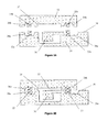
Figures 1A and 1B show a first example of the present invention, having a groove provided in a first layer and a recess provided in a second layer, before and after bonding, respectively; -
Figures 2A and 2B show a second example of the present invention, having both a groove and a recess provided in a first layer, before and after bonding, respectively; -
Figures 3A and 3B show a third example of the present invention, having a groove provided in both the first and second layers and a recess provided in a second layer, before and after bonding, respectively; -
Figures 4A and 4B show a fourth example of the present invention, having an electrical interconnect in combination with a vertical through conductor, before and after bonding, respectively; -
Figures 5A and 5B show a fifth example of the present invention, having an electrical interconnect material in combination with a vertical through conductor, before and after bonding, respectively; and -
Figures 6A and 6B show a sixth example of the present invention, having an electrical interconnect in combination with an electrode, before and after bonding, respectively. -
Figure 1A is a cross-section side view of afirst layer 11 and asecond layer 12 before a bonding process takes place according to a first example of the present invention. - The
first layer 11 comprises anelement 10, for example an accelerometer. Thesecond layer 12 comprises arecess 15 provided on the surface that is to be bonded to thefirst layer 11. - The
element 10 is surrounded by agroove 14 which provides a boundary around theelement 10 and recess 15. Thegroove 14 is, ideally, etched into the surface of thefirst layer 11. Thegroove 14 could, however, be provided in either, or indeed both, the surfaces of the first andsecond layers - Inside the
groove 14 is provided afirst portion 13a of sealingmaterial 13, for example metal sealant. Asecond portion 13b of sealingmaterial 13 is provided on the surface of thesecond layer 12, surrounding therecess 15. Thesecond portion 13b of sealingmaterial 13 has, in this example, a similar thickness to thefirst portion 13a of sealingmaterial 13 and is arranged to be aligned with thefirst portion 13a of sealingmaterial 13 when the first andsecond layers Figure 1A . - When the first and
second layers Figure 1B , the first andsecond portions material 13 are brought into contact causing the sealingmaterial 13 to deform laterally within thegroove 14, thereby creating a seal around theelement 10, as shown inFigure 1B . The seal is, preferably, a hermetic seal. - Of course, it will be appreciated that it is not essential that the first and second portions of sealing material are of similar thickness. Furthermore, the first and second portions of sealing material may have different heights and widths, provided that their combined height is greater than the depth of the groove and their width is configured such that, when the first and second layers are bonded together, the sealing material is laterally deformed and, furthermore, entirely retained within the groove.
- Indeed, whilst the amount of sealing material provided should be sufficient to ensure that it deforms within the groove, this amount should not be so great that it cannot be entirely accommodated within the groove after the first and second layers have been bonded together. This ensures that the surfaces of the first and second layers are in direct contact, lying adjacent to and flat against one another, after bonding has taken place.
- An important feature is therefore that the depth of the groove should be smaller than the overall, combined, thickness of the sealing material to ensure a proper squeeze of the sealing material during the sealing process, but wide enough to fully accommodate the lateral deformation of sealing material.
- It will also be appreciated that, in any embodiment of the present invention, sealing material need only be provided in the groove, or on the surface of the second layer, and not necessarily both, provided a sufficient amount of sealing material is provided to ensure that it is squeezed between the layers and hence deformed within the groove to form a seal when the first and second layers are bonded together, as explained above.
- Clearly, if the sealing material is not provided within the groove on one of the layers it should be arranged on the surface of the other layer such that when the first and second layers are bonded together it deforms within the groove.
- Once the first and
second layers recess 15 provides agap 17 above theelement 10. Since therecess 15 is formed in thesecond layer 12 before bonding takes place, and because the surfaces of the first andsecond layers material 13 being completely contained within thegroove 14, the known depth of therecess 15 in thesecond layer 12 is therefore the exact height of thegap 17 provided above theelement 10 after bonding. - It can be seen from
Figure 1B that only part of thegroove 14 is fully sealed by thesecond layer 12 in this example and, further, that anelectrical contact 16 may also be provided in part of thegroove 14 on the structure to allow electronic signals to pass to and from theelement 10. -
Figures 2A and 2B show a second a further example of the present invention, which is essentially the same as the first example, with the exception that no recess is provided in the surface of thesecond layer 22. Instead, thegap 27 is created and its dimensions controlled by forming arecess 25 in the surface of thefirst layer 21 by positioning the element 20 a predetermined and precise amount below the surface of the first layer, thereby effectively providing a preciselydimensioned gap 27 between theelement 20 and the surface of thesecond layer 22. - As with the previous example, a
groove 24 containing deformedsealing material 13 provides a seal around theelement 20. It will be appreciated, however, that although in this example thegroove 24 is provided in the surface of the first layer, the groove could be provided in the surface of thesecond layer 22 to provide the same result. - Alternatively, in a third example of the present invention, as shown in
figures 3A and 3B , agroove second layers sealing material grooves sealing material 33 is deformedly retained in thegrooves element 30. - It will, of course, be appreciated that the
recess 35 could be provided on the surface of either the first orsecond layer gap 37 between theelement 30 and the surface of thesecond layer 32. - Alternatively, a recess could be provided in the surfaces of both the first and second layers and/or a groove could be provided on the surface of both layers, if desired.
- Accordingly, the invention can be performed by providing the groove or recess on either the first or second layer surfaces, or even both, if desired.
- A fourth example of the present invention is shown in
Figure 4A , which comprises a similar arrangement to the examples described above. This further example, however, has the additional feature of a vertical throughconductor 49, also sometimes called a through silicon via (TSV), provided in thesecond layer 42. TheTSV 49 provides an electrical connection between acontact 46, provided on an upper surface of thesecond layer 42, and thefirst layer 41, as follows. - A
first portion 48a ofelectrical connection material 48, for example gold or copper, is provided in thegroove 44 that is formed in the surface of thefirst layer 41 and surrounds theelement 40. Theelectrical interconnect material 48 can be arranged either on theelement 40 side of the sealingmaterial 43, or on the outer side of the sealingmaterial 43. - A corresponding
second portion 48b of, ideally, the same, or a similar,electrical interconnect material 48 is arranged on a lower surface of thesecond layer 42. In this example, theTSV 45 is arranged to pass through thesecond layer 42 so that it connects theelectrical contact 46 on the upper surface of thesecond layer 42 with thesecond portion 48b ofelectrical interconnect material 48 provided on the lower surface of thesecond layer 42. Of course, a TSV could alternatively, be arranged to pass through thefirst layer 41 or, indeed, both first andsecond layers - In a similar manner as the seal formed by the sealing
material 43, sufficientelectrical interconnect material 48 is provided so that when the first andsecond layers second portions electrical interconnect material 48 being squeezed together such that they deform within thegroove 44 to form a secure electrical connection. As with the sealing material, the heights and widths of the electrical interconnect material can vary, provided that it is caused to deform within the groove when the first and second layers are bonded together. -
Figure 4B shows thefirst layer 41 and thesecond layer 42 joined together after bonding. As with the previous examples, the sealingmaterial 43 in thegroove 44 has been squeezed together and has subsequently deformed to provide a seal around theelement 40. In addition, theelectrical interconnect material 48 has also been squeezed together and deformed within thegroove 44 to provide a secure electrical connection. - The
groove 44 must therefore be of an appropriate size to accommodate both the sealingmaterial 43 and theelectrical interconnect material 48 after deformation, such that the surfaces of thefirst layer 41 and thesecond layer 42 are in full contact after bonding has taken place. Alternatively, an electrical connection could be formed by theelectrical interconnect material 48 being deformed within a separate groove portion (not shown). - In addition, the
groove 44 may be fully covered by thesecond layer 42, as shown in the example ofFigure 4B . - As previously explained, the sealing
material 43 and/or,electrical interconnect material 48 could alternatively be provided only on the surface of one of thelayers material groove 44 that it is intended to deform in such that when thelayers groove 44. -
Figures 5A and 5B show a fifth example of the present invention that is substantially the same as the fourth example described above, with the exception that thegroove 54 is provided in the surface of thesecond layer 52 and therecess 55 is provided in the surface of thefirst layer 51. - Furthermore, in this example, the sealing
material 53 andelectrical interconnect material 58 are only provided on the first layer. However, as outlined previously, sufficient amounts of sealingmaterial 53 andelectrical interconnect material 58 are provided to ensure that their respective heights are both greater than the depth of thegroove 54. Thus, when the first andsecond layers material 53 andelectrical interconnect material 58 are both deformedly retained within thegroove 54, as can clearly be seen fromFigure 5B . - It can also be seen how a
gap 57 is formed between theelement 50 provided in thefirst layer 51 and the surface of thesecond layer 52, the dimensions of thegap 57 being accurately controlled by the dimensions of therecess 55. - The TSV may be replaced by, for example, an electrode or a patterned structure/layer.
Figures 6A and 6B show a sixth example of the present invention that is substantially the same as the fourth example, with the exception that the TSV has been replaced by anelectrode 66 situated, in this example, in therecess 65 formed in the surface of thesecond layer 62. - In
Figure 6B it can be seen how the first andsecond portions electrical interconnect material 68 are aligned such that, on bonding the first andsecond layers second portions interconnect material 68 are squeezed together such that they are deformed, in the same manner as the first andsecond portions material 63, in a portion ofgroove 64, to form an electrical connection between thefirst layer 61 and theelectrode 66 provided on the surface of thesecond layer 62. - As mentioned above, the electrode could be substituted by a patterned structure or one or more component(s) suitable for sending and/or receiving an electrical signal.
- As will be understood from the above described examples, an advantage of the present invention is that the dimensions of a gap provided above an element can be accurately created and controlled independently of the sealing process between two layers. The present invention enables gap dimension control to be extremely accurate, even when providing a hermetic seal around an element when bonding two layers, because it is known that the surfaces of the layers will be in full surface contact with one another.
- In particular, the present invention eliminates the variable of the gap dimension, previously introduced by an inability to accurately control the thickness of sealing material between two bonded layers, when designing components requiring accurately controlled gap dimensions. In addition, the thickness of the seal can be controlled by the amount of sealing material provided, together with the depth and width of the groove without having any effect on the gap provided above the element.
Claims (14)
- A structure having a gap provided between a portion of two layers that are joined together, the structure comprising:a first layer having an element formed within a first surface;a second layer having a second surface, adjacent to and in direct contact with at least a portion of the first surface on all sides of the element such that the element is completely enclosed;a recess of predetermined depth arranged to provide the gap between the element and the second surface;a groove formed in one of the first surface or second surface, the groove defining a boundary around the element; andsealing material deformedly retained completely within the groove to form a seal around the element, such that the recess defines the gap.
- The structure of claim 1, wherein the element is substantially coplanar with the first surface of the first layer and the recess is formed in the second surface of the second layer to a predetermined depth equal to the height of the gap desired.
- The structure of claim 1, wherein the recess is formed by the element being recessed below the first surface of the first layer by a predetermined depth equal to the height of the gap desired.
- The structure of any preceding claim, wherein a groove is formed in both the first surface of the first layer and the second surface of the second layer.
- The structure of any preceding claim, wherein the one or more grooves are completely covered between the first layer and second layer.
- The structure of any preceding claim, further comprising an electrical interconnect material deformedly retained within at least a portion of the groove.
- The structure of claim 6, further comprising a vertical through conductor provided in one of the first or second layer and arranged to electrically connect a surface of said first or second layer with the other first or second layer via the electrical interconnect material.
- The structure of claim 6, further comprising an electrode or a patterned structure provided on a surface of one of the first or second layer and arranged to electrically connect with the other first or second layer via the electrical interconnect material.
- A method of accurately controlling the dimensions of a gap provided between a portion of two layers joined together, the method comprising the steps of:providing a first layer with an element formed within a first surface;providing a second layer with a second surface;forming a recess in one of the first surface or second surface, the recess having a predetermined depth;forming a groove in one of the first surface or second surface, the groove defining a boundary for surrounding the element;providing sealing material on at least one of the first surface or second surface; andjoining the first layer and second layer together such that the second surface is adjacent to and in direct contact with at least a portion of the first surface on all sides of the element thereby completely enclosing the element,wherein the sealing material is arranged to be deformedly retained completely within the groove such that the recess defines the gap.
- The method of claim 9, further comprising the step of forming the recess in the first surface by recessing the element below the first surface of the first layer to a predetermined depth equal to the gap desired.
- The method of claim 9 or 10, further comprising the step of forming a groove in both the first surface of the first layer and the second surface of the second layer.
- The method of any one of claims 9 to 11, wherein the overall height of the sealing material provided on the at least one of the first surface or second surface is greater than the combined depth of the one or more grooves.
- The method of any one of claims 9 to 12, further comprising the step of completely covering the one or more grooves between the first layer and second layer when the first and second layer are bonded together.
- The method of any one of claims 9 to 13, further comprising the step of providing an electrical interconnect material on at least one of the first surface or second surface, wherein the electrical interconnect material is arranged to be deformedly retained completely within a portion of the groove when the first layer and second layer are bonded together.
Priority Applications (2)
| Application Number | Priority Date | Filing Date | Title |
|---|---|---|---|
| EP09161583.1A EP2259018B1 (en) | 2009-05-29 | 2009-05-29 | Gap control for die or layer bonding using intermediate layers of a micro-electromechanical system |
| US12/800,727 US8421169B2 (en) | 2009-05-29 | 2010-05-21 | Gap control for die or layer bonding using intermediate layers |
Applications Claiming Priority (1)
| Application Number | Priority Date | Filing Date | Title |
|---|---|---|---|
| EP09161583.1A EP2259018B1 (en) | 2009-05-29 | 2009-05-29 | Gap control for die or layer bonding using intermediate layers of a micro-electromechanical system |
Publications (2)
| Publication Number | Publication Date |
|---|---|
| EP2259018A1 true EP2259018A1 (en) | 2010-12-08 |
| EP2259018B1 EP2259018B1 (en) | 2017-06-28 |
Family
ID=41198644
Family Applications (1)
| Application Number | Title | Priority Date | Filing Date |
|---|---|---|---|
| EP09161583.1A Not-in-force EP2259018B1 (en) | 2009-05-29 | 2009-05-29 | Gap control for die or layer bonding using intermediate layers of a micro-electromechanical system |
Country Status (2)
| Country | Link |
|---|---|
| US (1) | US8421169B2 (en) |
| EP (1) | EP2259018B1 (en) |
Cited By (3)
| Publication number | Priority date | Publication date | Assignee | Title |
|---|---|---|---|---|
| DE102012217853B4 (en) * | 2011-10-04 | 2016-02-04 | Institut für Mikroelektronik- und Mechatronik-Systeme gGmbH | Arrangement for generating a defined spacing between electrode surfaces on integrated components for chemical and biochemical sensors |
| ITUA20164673A1 (en) * | 2016-06-27 | 2017-12-27 | St Microelectronics Srl | MEMS DEVICE FORMED BY AT LEAST TWO MULTI-PURPOSED STRUCTURAL LAYERS AND RELATIVE PROCESS OF MANUFACTURE |
| EP3261117B1 (en) * | 2016-06-22 | 2020-11-18 | Commissariat à l'Energie Atomique et aux Energies Alternatives | Microelectronic device housing |
Families Citing this family (15)
| Publication number | Priority date | Publication date | Assignee | Title |
|---|---|---|---|---|
| US8507358B2 (en) * | 2010-08-27 | 2013-08-13 | Taiwan Semiconductor Manufacturing Company, Ltd. | Composite wafer semiconductor |
| US20120211805A1 (en) | 2011-02-22 | 2012-08-23 | Bernhard Winkler | Cavity structures for mems devices |
| US9586811B2 (en) | 2011-06-10 | 2017-03-07 | Taiwan Semiconductor Manufacturing Company, Ltd. | Semiconductor devices with moving members and methods for making the same |
| DE102012206869B4 (en) * | 2012-04-25 | 2021-05-27 | Robert Bosch Gmbh | Micromechanical component and method for producing a micromechanical component |
| US9136136B2 (en) | 2013-09-19 | 2015-09-15 | Infineon Technologies Dresden Gmbh | Method and structure for creating cavities with extreme aspect ratios |
| CN103910325B (en) * | 2014-02-27 | 2015-06-17 | 厦门大学 | High-reliability micro-electromechanical system (MEMS) packaging structure and method capable of achieving accurate control of bonding gap |
| US20150262902A1 (en) | 2014-03-12 | 2015-09-17 | Invensas Corporation | Integrated circuits protected by substrates with cavities, and methods of manufacture |
| CN105084294A (en) * | 2014-04-21 | 2015-11-25 | 中芯国际集成电路制造(上海)有限公司 | MEMS device, preparation method thereof and electronic device |
| US10002844B1 (en) | 2016-12-21 | 2018-06-19 | Invensas Bonding Technologies, Inc. | Bonded structures |
| TWI738947B (en) * | 2017-02-09 | 2021-09-11 | 美商英帆薩斯邦德科技有限公司 | Bonded structures and method of forming the same |
| US10508030B2 (en) | 2017-03-21 | 2019-12-17 | Invensas Bonding Technologies, Inc. | Seal for microelectronic assembly |
| US10923408B2 (en) | 2017-12-22 | 2021-02-16 | Invensas Bonding Technologies, Inc. | Cavity packages |
| US11380597B2 (en) | 2017-12-22 | 2022-07-05 | Invensas Bonding Technologies, Inc. | Bonded structures |
| US11004757B2 (en) | 2018-05-14 | 2021-05-11 | Invensas Bonding Technologies, Inc. | Bonded structures |
| US12374641B2 (en) | 2019-06-12 | 2025-07-29 | Adeia Semiconductor Bonding Technologies Inc. | Sealed bonded structures and methods for forming the same |
Citations (8)
| Publication number | Priority date | Publication date | Assignee | Title |
|---|---|---|---|---|
| GB2212274A (en) * | 1987-11-09 | 1989-07-19 | Vaisala Oy | Capacitive accelerometer and its fabrication method |
| EP0640784A1 (en) * | 1993-08-31 | 1995-03-01 | Applied Materials, Inc. | Heated removable throttle valve |
| DE19938205A1 (en) * | 1999-08-12 | 2001-02-15 | Bosch Gmbh Robert | Micro-mechanical sensor has improved sealing arrangement between upper cover and lower sensor to provide an effective hermetic seal between the two without unwanted sealant leakage into the sensor measurement area |
| US20020007149A1 (en) | 2000-03-23 | 2002-01-17 | Nelson Sheldon J. | Single use disposable jet injector |
| US20030089394A1 (en) * | 2001-10-25 | 2003-05-15 | Chang-Chien Patty P.L. | Method and system for locally sealing a vacuum microcavity, Methods and systems for monitoring and controlling pressure and method and system for trimming resonant frequency of a microstructure therein |
| WO2006061792A2 (en) | 2004-12-10 | 2006-06-15 | Koninklijke Philips Electronics N.V. | Hermetically sealed integrated circuit package |
| US20080123297A1 (en) | 2006-05-15 | 2008-05-29 | Isothermal Systems Research, Inc. | Hybrid clamshell blade system |
| WO2009022498A1 (en) * | 2007-08-10 | 2009-02-19 | Murata Manufacturing Co., Ltd. | Electronic component manufacturing method |
Family Cites Families (3)
| Publication number | Priority date | Publication date | Assignee | Title |
|---|---|---|---|---|
| US7121402B2 (en) * | 2003-04-09 | 2006-10-17 | Reactive Nano Technologies, Inc | Container hermetically sealed with crushable material and reactive multilayer material |
| KR100447851B1 (en) * | 2002-11-14 | 2004-09-08 | 삼성전자주식회사 | Wafer level Bonding method of flip-chip manner for semiconductor apparatus in lateral bonded type |
| FR2849013B1 (en) * | 2002-12-20 | 2005-03-11 | Commissariat Energie Atomique | ENCAPSULATION COMPONENT OF INTEGRATED ELECTROMECHANICAL MICRO-SYSTEMS AND METHOD FOR PRODUCING THE COMPONENT |
-
2009
- 2009-05-29 EP EP09161583.1A patent/EP2259018B1/en not_active Not-in-force
-
2010
- 2010-05-21 US US12/800,727 patent/US8421169B2/en not_active Expired - Fee Related
Patent Citations (8)
| Publication number | Priority date | Publication date | Assignee | Title |
|---|---|---|---|---|
| GB2212274A (en) * | 1987-11-09 | 1989-07-19 | Vaisala Oy | Capacitive accelerometer and its fabrication method |
| EP0640784A1 (en) * | 1993-08-31 | 1995-03-01 | Applied Materials, Inc. | Heated removable throttle valve |
| DE19938205A1 (en) * | 1999-08-12 | 2001-02-15 | Bosch Gmbh Robert | Micro-mechanical sensor has improved sealing arrangement between upper cover and lower sensor to provide an effective hermetic seal between the two without unwanted sealant leakage into the sensor measurement area |
| US20020007149A1 (en) | 2000-03-23 | 2002-01-17 | Nelson Sheldon J. | Single use disposable jet injector |
| US20030089394A1 (en) * | 2001-10-25 | 2003-05-15 | Chang-Chien Patty P.L. | Method and system for locally sealing a vacuum microcavity, Methods and systems for monitoring and controlling pressure and method and system for trimming resonant frequency of a microstructure therein |
| WO2006061792A2 (en) | 2004-12-10 | 2006-06-15 | Koninklijke Philips Electronics N.V. | Hermetically sealed integrated circuit package |
| US20080123297A1 (en) | 2006-05-15 | 2008-05-29 | Isothermal Systems Research, Inc. | Hybrid clamshell blade system |
| WO2009022498A1 (en) * | 2007-08-10 | 2009-02-19 | Murata Manufacturing Co., Ltd. | Electronic component manufacturing method |
Cited By (7)
| Publication number | Priority date | Publication date | Assignee | Title |
|---|---|---|---|---|
| DE102012217853B4 (en) * | 2011-10-04 | 2016-02-04 | Institut für Mikroelektronik- und Mechatronik-Systeme gGmbH | Arrangement for generating a defined spacing between electrode surfaces on integrated components for chemical and biochemical sensors |
| EP3261117B1 (en) * | 2016-06-22 | 2020-11-18 | Commissariat à l'Energie Atomique et aux Energies Alternatives | Microelectronic device housing |
| ITUA20164673A1 (en) * | 2016-06-27 | 2017-12-27 | St Microelectronics Srl | MEMS DEVICE FORMED BY AT LEAST TWO MULTI-PURPOSED STRUCTURAL LAYERS AND RELATIVE PROCESS OF MANUFACTURE |
| EP3263517A1 (en) * | 2016-06-27 | 2018-01-03 | STMicroelectronics S.r.l. | Mems device formed by at least two bonded structural layers and manufacturing process thereof |
| US10227233B2 (en) | 2016-06-27 | 2019-03-12 | Stmicroelectronics S.R.L. | MEMS device formed by at least two bonded structural layers and manufacturing process thereof |
| US10570009B2 (en) | 2016-06-27 | 2020-02-25 | Stmicroelectronics S.R.L. | MEMS device formed by at least two bonded structural layers and manufacturing process thereof |
| US10954121B2 (en) | 2016-06-27 | 2021-03-23 | Stmicroelectronics S.R.L. | MEMS device formed by at least two bonded structural layers and manufacturing process thereof |
Also Published As
| Publication number | Publication date |
|---|---|
| US8421169B2 (en) | 2013-04-16 |
| EP2259018B1 (en) | 2017-06-28 |
| US20100301432A1 (en) | 2010-12-02 |
Similar Documents
| Publication | Publication Date | Title |
|---|---|---|
| US8421169B2 (en) | Gap control for die or layer bonding using intermediate layers | |
| EP2121511B1 (en) | Method of packaging an electronic or micromechanical component | |
| US20050205951A1 (en) | Flip chip bonded micro-electromechanical system (MEMS) device | |
| US9422152B2 (en) | Hybridly integrated module having a sealing structure | |
| US8021906B2 (en) | Hermetic sealing and electrical contacting of a microelectromechanical structure, and microsystem (MEMS) produced therewith | |
| JP2009516598A (en) | Method for producing microelectromechanical component and microelectromechanical component | |
| JP2006116694A (en) | Hermetically sealed microdevice with getter shield | |
| US10266392B2 (en) | Environment-resistant module, micropackage and methods of manufacturing same | |
| JP2013030759A (en) | Packaged device, packaging method and production method of package material | |
| US9051172B2 (en) | Method for manufacturing a hermetically sealed structure | |
| CN101346815B (en) | Microelectronic machine and method for manufacturing same | |
| US7507346B2 (en) | Method for manufacturing electronic component, and electronic component | |
| TW201708095A (en) | MEMS device with electrodes permeable to outgassing species | |
| JP2008182014A (en) | Package substrate and manufacturing method thereof | |
| JP4268480B2 (en) | Electronic component sealing substrate and electronic device using the same | |
| JP2018006577A (en) | Manufacturing method for semiconductor device | |
| JP6569382B2 (en) | Manufacturing method of electronic device | |
| JP4957123B2 (en) | Sensor unit and manufacturing method thereof | |
| EP2481704B1 (en) | Edge-mounted sensor | |
| JP2011204950A (en) | Metal embedded glass substrate and method of manufacturing the same, and mems device | |
| JP5072555B2 (en) | Electronic device package | |
| JP2011500343A (en) | Multilayer bump structure and manufacturing method thereof | |
| JP4505671B2 (en) | Signal extraction structure for semiconductor microelectromechanical devices | |
| US12631665B2 (en) | Inertial sensor, method for manufacturing inertial sensor, and inertial measurement unit | |
| US20230221346A1 (en) | Inertial sensor, method for manufacturing inertial sensor, and inertial measurement unit |
Legal Events
| Date | Code | Title | Description |
|---|---|---|---|
| PUAI | Public reference made under article 153(3) epc to a published international application that has entered the european phase |
Free format text: ORIGINAL CODE: 0009012 |
|
| AK | Designated contracting states |
Kind code of ref document: A1 Designated state(s): AT BE BG CH CY CZ DE DK EE ES FI FR GB GR HR HU IE IS IT LI LT LU LV MC MK MT NL NO PL PT RO SE SI SK TR |
|
| 17P | Request for examination filed |
Effective date: 20110603 |
|
| 17Q | First examination report despatched |
Effective date: 20120118 |
|
| GRAP | Despatch of communication of intention to grant a patent |
Free format text: ORIGINAL CODE: EPIDOSNIGR1 |
|
| RIC1 | Information provided on ipc code assigned before grant |
Ipc: H01L 23/31 20060101ALI20161213BHEP Ipc: H01L 23/10 20060101ALI20161213BHEP Ipc: G01P 15/08 20060101ALI20161213BHEP Ipc: G01C 19/56 20120101AFI20161213BHEP Ipc: G01P 15/125 20060101ALI20161213BHEP Ipc: B81B 7/00 20060101ALI20161213BHEP Ipc: B81C 1/00 20060101ALI20161213BHEP |
|
| INTG | Intention to grant announced |
Effective date: 20170113 |
|
| GRAS | Grant fee paid |
Free format text: ORIGINAL CODE: EPIDOSNIGR3 |
|
| GRAA | (expected) grant |
Free format text: ORIGINAL CODE: 0009210 |
|
| AK | Designated contracting states |
Kind code of ref document: B1 Designated state(s): AT BE BG CH CY CZ DE DK EE ES FI FR GB GR HR HU IE IS IT LI LT LU LV MC MK MT NL NO PL PT RO SE SI SK TR |
|
| REG | Reference to a national code |
Ref country code: GB Ref legal event code: FG4D |
|
| REG | Reference to a national code |
Ref country code: CH Ref legal event code: EP |
|
| REG | Reference to a national code |
Ref country code: AT Ref legal event code: REF Ref document number: 905275 Country of ref document: AT Kind code of ref document: T Effective date: 20170715 |
|
| REG | Reference to a national code |
Ref country code: IE Ref legal event code: FG4D |
|
| REG | Reference to a national code |
Ref country code: DE Ref legal event code: R096 Ref document number: 602009046823 Country of ref document: DE |
|
| PG25 | Lapsed in a contracting state [announced via postgrant information from national office to epo] |
Ref country code: GR Free format text: LAPSE BECAUSE OF FAILURE TO SUBMIT A TRANSLATION OF THE DESCRIPTION OR TO PAY THE FEE WITHIN THE PRESCRIBED TIME-LIMIT Effective date: 20170929 Ref country code: HR Free format text: LAPSE BECAUSE OF FAILURE TO SUBMIT A TRANSLATION OF THE DESCRIPTION OR TO PAY THE FEE WITHIN THE PRESCRIBED TIME-LIMIT Effective date: 20170628 Ref country code: LT Free format text: LAPSE BECAUSE OF FAILURE TO SUBMIT A TRANSLATION OF THE DESCRIPTION OR TO PAY THE FEE WITHIN THE PRESCRIBED TIME-LIMIT Effective date: 20170628 Ref country code: NO Free format text: LAPSE BECAUSE OF FAILURE TO SUBMIT A TRANSLATION OF THE DESCRIPTION OR TO PAY THE FEE WITHIN THE PRESCRIBED TIME-LIMIT Effective date: 20170928 Ref country code: FI Free format text: LAPSE BECAUSE OF FAILURE TO SUBMIT A TRANSLATION OF THE DESCRIPTION OR TO PAY THE FEE WITHIN THE PRESCRIBED TIME-LIMIT Effective date: 20170628 |
|
| REG | Reference to a national code |
Ref country code: NL Ref legal event code: MP Effective date: 20170628 |
|
| REG | Reference to a national code |
Ref country code: LT Ref legal event code: MG4D |
|
| REG | Reference to a national code |
Ref country code: AT Ref legal event code: MK05 Ref document number: 905275 Country of ref document: AT Kind code of ref document: T Effective date: 20170628 |
|
| PG25 | Lapsed in a contracting state [announced via postgrant information from national office to epo] |
Ref country code: NL Free format text: LAPSE BECAUSE OF FAILURE TO SUBMIT A TRANSLATION OF THE DESCRIPTION OR TO PAY THE FEE WITHIN THE PRESCRIBED TIME-LIMIT Effective date: 20170628 Ref country code: BG Free format text: LAPSE BECAUSE OF FAILURE TO SUBMIT A TRANSLATION OF THE DESCRIPTION OR TO PAY THE FEE WITHIN THE PRESCRIBED TIME-LIMIT Effective date: 20170928 Ref country code: LV Free format text: LAPSE BECAUSE OF FAILURE TO SUBMIT A TRANSLATION OF THE DESCRIPTION OR TO PAY THE FEE WITHIN THE PRESCRIBED TIME-LIMIT Effective date: 20170628 Ref country code: SE Free format text: LAPSE BECAUSE OF FAILURE TO SUBMIT A TRANSLATION OF THE DESCRIPTION OR TO PAY THE FEE WITHIN THE PRESCRIBED TIME-LIMIT Effective date: 20170628 |
|
| PG25 | Lapsed in a contracting state [announced via postgrant information from national office to epo] |
Ref country code: AT Free format text: LAPSE BECAUSE OF FAILURE TO SUBMIT A TRANSLATION OF THE DESCRIPTION OR TO PAY THE FEE WITHIN THE PRESCRIBED TIME-LIMIT Effective date: 20170628 Ref country code: RO Free format text: LAPSE BECAUSE OF FAILURE TO SUBMIT A TRANSLATION OF THE DESCRIPTION OR TO PAY THE FEE WITHIN THE PRESCRIBED TIME-LIMIT Effective date: 20170628 Ref country code: SK Free format text: LAPSE BECAUSE OF FAILURE TO SUBMIT A TRANSLATION OF THE DESCRIPTION OR TO PAY THE FEE WITHIN THE PRESCRIBED TIME-LIMIT Effective date: 20170628 Ref country code: CZ Free format text: LAPSE BECAUSE OF FAILURE TO SUBMIT A TRANSLATION OF THE DESCRIPTION OR TO PAY THE FEE WITHIN THE PRESCRIBED TIME-LIMIT Effective date: 20170628 Ref country code: EE Free format text: LAPSE BECAUSE OF FAILURE TO SUBMIT A TRANSLATION OF THE DESCRIPTION OR TO PAY THE FEE WITHIN THE PRESCRIBED TIME-LIMIT Effective date: 20170628 |
|
| PG25 | Lapsed in a contracting state [announced via postgrant information from national office to epo] |
Ref country code: PL Free format text: LAPSE BECAUSE OF FAILURE TO SUBMIT A TRANSLATION OF THE DESCRIPTION OR TO PAY THE FEE WITHIN THE PRESCRIBED TIME-LIMIT Effective date: 20170628 Ref country code: IT Free format text: LAPSE BECAUSE OF FAILURE TO SUBMIT A TRANSLATION OF THE DESCRIPTION OR TO PAY THE FEE WITHIN THE PRESCRIBED TIME-LIMIT Effective date: 20170628 Ref country code: ES Free format text: LAPSE BECAUSE OF FAILURE TO SUBMIT A TRANSLATION OF THE DESCRIPTION OR TO PAY THE FEE WITHIN THE PRESCRIBED TIME-LIMIT Effective date: 20170628 Ref country code: IS Free format text: LAPSE BECAUSE OF FAILURE TO SUBMIT A TRANSLATION OF THE DESCRIPTION OR TO PAY THE FEE WITHIN THE PRESCRIBED TIME-LIMIT Effective date: 20171028 |
|
| REG | Reference to a national code |
Ref country code: DE Ref legal event code: R097 Ref document number: 602009046823 Country of ref document: DE |
|
| PG25 | Lapsed in a contracting state [announced via postgrant information from national office to epo] |
Ref country code: DK Free format text: LAPSE BECAUSE OF FAILURE TO SUBMIT A TRANSLATION OF THE DESCRIPTION OR TO PAY THE FEE WITHIN THE PRESCRIBED TIME-LIMIT Effective date: 20170628 |
|
| PLBE | No opposition filed within time limit |
Free format text: ORIGINAL CODE: 0009261 |
|
| STAA | Information on the status of an ep patent application or granted ep patent |
Free format text: STATUS: NO OPPOSITION FILED WITHIN TIME LIMIT |
|
| 26N | No opposition filed |
Effective date: 20180329 |
|
| PG25 | Lapsed in a contracting state [announced via postgrant information from national office to epo] |
Ref country code: SI Free format text: LAPSE BECAUSE OF FAILURE TO SUBMIT A TRANSLATION OF THE DESCRIPTION OR TO PAY THE FEE WITHIN THE PRESCRIBED TIME-LIMIT Effective date: 20170628 |
|
| REG | Reference to a national code |
Ref country code: CH Ref legal event code: PL |
|
| GBPC | Gb: european patent ceased through non-payment of renewal fee |
Effective date: 20180529 |
|
| REG | Reference to a national code |
Ref country code: BE Ref legal event code: MM Effective date: 20180531 |
|
| PG25 | Lapsed in a contracting state [announced via postgrant information from national office to epo] |
Ref country code: MC Free format text: LAPSE BECAUSE OF FAILURE TO SUBMIT A TRANSLATION OF THE DESCRIPTION OR TO PAY THE FEE WITHIN THE PRESCRIBED TIME-LIMIT Effective date: 20170628 |
|
| REG | Reference to a national code |
Ref country code: IE Ref legal event code: MM4A |
|
| PG25 | Lapsed in a contracting state [announced via postgrant information from national office to epo] |
Ref country code: CH Free format text: LAPSE BECAUSE OF NON-PAYMENT OF DUE FEES Effective date: 20180531 Ref country code: LI Free format text: LAPSE BECAUSE OF NON-PAYMENT OF DUE FEES Effective date: 20180531 |
|
| PG25 | Lapsed in a contracting state [announced via postgrant information from national office to epo] |
Ref country code: LU Free format text: LAPSE BECAUSE OF NON-PAYMENT OF DUE FEES Effective date: 20180529 |
|
| PG25 | Lapsed in a contracting state [announced via postgrant information from national office to epo] |
Ref country code: IE Free format text: LAPSE BECAUSE OF NON-PAYMENT OF DUE FEES Effective date: 20180529 Ref country code: FR Free format text: LAPSE BECAUSE OF NON-PAYMENT OF DUE FEES Effective date: 20180531 Ref country code: GB Free format text: LAPSE BECAUSE OF NON-PAYMENT OF DUE FEES Effective date: 20180529 |
|
| PG25 | Lapsed in a contracting state [announced via postgrant information from national office to epo] |
Ref country code: BE Free format text: LAPSE BECAUSE OF NON-PAYMENT OF DUE FEES Effective date: 20180531 |
|
| PGFP | Annual fee paid to national office [announced via postgrant information from national office to epo] |
Ref country code: DE Payment date: 20190724 Year of fee payment: 11 |
|
| PG25 | Lapsed in a contracting state [announced via postgrant information from national office to epo] |
Ref country code: MT Free format text: LAPSE BECAUSE OF NON-PAYMENT OF DUE FEES Effective date: 20180529 |
|
| PG25 | Lapsed in a contracting state [announced via postgrant information from national office to epo] |
Ref country code: TR Free format text: LAPSE BECAUSE OF FAILURE TO SUBMIT A TRANSLATION OF THE DESCRIPTION OR TO PAY THE FEE WITHIN THE PRESCRIBED TIME-LIMIT Effective date: 20170628 |
|
| PG25 | Lapsed in a contracting state [announced via postgrant information from national office to epo] |
Ref country code: PT Free format text: LAPSE BECAUSE OF FAILURE TO SUBMIT A TRANSLATION OF THE DESCRIPTION OR TO PAY THE FEE WITHIN THE PRESCRIBED TIME-LIMIT Effective date: 20170628 Ref country code: HU Free format text: LAPSE BECAUSE OF FAILURE TO SUBMIT A TRANSLATION OF THE DESCRIPTION OR TO PAY THE FEE WITHIN THE PRESCRIBED TIME-LIMIT; INVALID AB INITIO Effective date: 20090529 |
|
| PG25 | Lapsed in a contracting state [announced via postgrant information from national office to epo] |
Ref country code: MK Free format text: LAPSE BECAUSE OF NON-PAYMENT OF DUE FEES Effective date: 20170628 Ref country code: CY Free format text: LAPSE BECAUSE OF FAILURE TO SUBMIT A TRANSLATION OF THE DESCRIPTION OR TO PAY THE FEE WITHIN THE PRESCRIBED TIME-LIMIT Effective date: 20170628 |
|
| REG | Reference to a national code |
Ref country code: DE Ref legal event code: R119 Ref document number: 602009046823 Country of ref document: DE |
|
| PG25 | Lapsed in a contracting state [announced via postgrant information from national office to epo] |
Ref country code: DE Free format text: LAPSE BECAUSE OF NON-PAYMENT OF DUE FEES Effective date: 20201201 |