EP2257953B1 - Interface device and junction box for a htsc degaussing coil - Google Patents
Interface device and junction box for a htsc degaussing coil Download PDFInfo
- Publication number
- EP2257953B1 EP2257953B1 EP09725012.0A EP09725012A EP2257953B1 EP 2257953 B1 EP2257953 B1 EP 2257953B1 EP 09725012 A EP09725012 A EP 09725012A EP 2257953 B1 EP2257953 B1 EP 2257953B1
- Authority
- EP
- European Patent Office
- Prior art keywords
- interface
- conductor
- hts
- conductors
- substrate
- Prior art date
- Legal status (The legal status is an assumption and is not a legal conclusion. Google has not performed a legal analysis and makes no representation as to the accuracy of the status listed.)
- Active
Links
- 239000004020 conductor Substances 0.000 claims description 121
- 239000000758 substrate Substances 0.000 claims description 58
- 238000004804 winding Methods 0.000 claims description 16
- 239000000463 material Substances 0.000 claims description 15
- 239000002887 superconductor Substances 0.000 claims description 10
- 239000002826 coolant Substances 0.000 description 10
- 230000005291 magnetic effect Effects 0.000 description 6
- 238000005057 refrigeration Methods 0.000 description 6
- PZKRHHZKOQZHIO-UHFFFAOYSA-N [B].[B].[Mg] Chemical compound [B].[B].[Mg] PZKRHHZKOQZHIO-UHFFFAOYSA-N 0.000 description 4
- 229910021521 yttrium barium copper oxide Inorganic materials 0.000 description 4
- RYGMFSIKBFXOCR-UHFFFAOYSA-N Copper Chemical compound [Cu] RYGMFSIKBFXOCR-UHFFFAOYSA-N 0.000 description 3
- 239000011248 coating agent Substances 0.000 description 3
- 238000000576 coating method Methods 0.000 description 3
- 238000010586 diagram Methods 0.000 description 3
- 229920000642 polymer Polymers 0.000 description 3
- 238000005476 soldering Methods 0.000 description 3
- IJGRMHOSHXDMSA-UHFFFAOYSA-N Atomic nitrogen Chemical compound N#N IJGRMHOSHXDMSA-UHFFFAOYSA-N 0.000 description 2
- QPLDLSVMHZLSFG-UHFFFAOYSA-N Copper oxide Chemical compound [Cu]=O QPLDLSVMHZLSFG-UHFFFAOYSA-N 0.000 description 2
- 239000005751 Copper oxide Substances 0.000 description 2
- OSOKRZIXBNTTJX-UHFFFAOYSA-N [O].[Ca].[Cu].[Sr].[Bi] Chemical compound [O].[Ca].[Cu].[Sr].[Bi] OSOKRZIXBNTTJX-UHFFFAOYSA-N 0.000 description 2
- BTGZYWWSOPEHMM-UHFFFAOYSA-N [O].[Cu].[Y].[Ba] Chemical compound [O].[Cu].[Y].[Ba] BTGZYWWSOPEHMM-UHFFFAOYSA-N 0.000 description 2
- 229910052782 aluminium Inorganic materials 0.000 description 2
- XAGFODPZIPBFFR-UHFFFAOYSA-N aluminium Chemical compound [Al] XAGFODPZIPBFFR-UHFFFAOYSA-N 0.000 description 2
- 229910052802 copper Inorganic materials 0.000 description 2
- 239000010949 copper Substances 0.000 description 2
- 229910000431 copper oxide Inorganic materials 0.000 description 2
- 239000007789 gas Substances 0.000 description 2
- 239000007788 liquid Substances 0.000 description 2
- 230000004075 alteration Effects 0.000 description 1
- 238000004891 communication Methods 0.000 description 1
- 230000001419 dependent effect Effects 0.000 description 1
- 238000001514 detection method Methods 0.000 description 1
- 239000003822 epoxy resin Substances 0.000 description 1
- 239000003302 ferromagnetic material Substances 0.000 description 1
- 239000012530 fluid Substances 0.000 description 1
- 239000011888 foil Substances 0.000 description 1
- 239000001307 helium Substances 0.000 description 1
- 229910052734 helium Inorganic materials 0.000 description 1
- SWQJXJOGLNCZEY-UHFFFAOYSA-N helium atom Chemical compound [He] SWQJXJOGLNCZEY-UHFFFAOYSA-N 0.000 description 1
- 238000009413 insulation Methods 0.000 description 1
- 239000012212 insulator Substances 0.000 description 1
- 230000007774 longterm Effects 0.000 description 1
- 238000004519 manufacturing process Methods 0.000 description 1
- 229910052751 metal Inorganic materials 0.000 description 1
- 239000002184 metal Substances 0.000 description 1
- 238000000034 method Methods 0.000 description 1
- 229910052757 nitrogen Inorganic materials 0.000 description 1
- 229920003223 poly(pyromellitimide-1,4-diphenyl ether) Polymers 0.000 description 1
- 229920000647 polyepoxide Polymers 0.000 description 1
- 229920001721 polyimide Polymers 0.000 description 1
- 229920001343 polytetrafluoroethylene Polymers 0.000 description 1
- 238000007670 refining Methods 0.000 description 1
- 239000004065 semiconductor Substances 0.000 description 1
- 229910000679 solder Inorganic materials 0.000 description 1
- 229910001220 stainless steel Inorganic materials 0.000 description 1
- 239000010935 stainless steel Substances 0.000 description 1
- 230000001960 triggered effect Effects 0.000 description 1
Images


Classifications
-
- B—PERFORMING OPERATIONS; TRANSPORTING
- B63—SHIPS OR OTHER WATERBORNE VESSELS; RELATED EQUIPMENT
- B63G—OFFENSIVE OR DEFENSIVE ARRANGEMENTS ON VESSELS; MINE-LAYING; MINE-SWEEPING; SUBMARINES; AIRCRAFT CARRIERS
- B63G9/00—Other offensive or defensive arrangements on vessels against submarines, torpedoes, or mines
- B63G9/06—Other offensive or defensive arrangements on vessels against submarines, torpedoes, or mines for degaussing vessels
-
- H—ELECTRICITY
- H01—ELECTRIC ELEMENTS
- H01F—MAGNETS; INDUCTANCES; TRANSFORMERS; SELECTION OF MATERIALS FOR THEIR MAGNETIC PROPERTIES
- H01F13/00—Apparatus or processes for magnetising or demagnetising
- H01F13/006—Methods and devices for demagnetising of magnetic bodies, e.g. workpieces, sheet material
-
- H—ELECTRICITY
- H01—ELECTRIC ELEMENTS
- H01F—MAGNETS; INDUCTANCES; TRANSFORMERS; SELECTION OF MATERIALS FOR THEIR MAGNETIC PROPERTIES
- H01F6/00—Superconducting magnets; Superconducting coils
- H01F6/06—Coils, e.g. winding, insulating, terminating or casing arrangements therefor
- H01F6/065—Feed-through bushings, terminals and joints
-
- Y—GENERAL TAGGING OF NEW TECHNOLOGICAL DEVELOPMENTS; GENERAL TAGGING OF CROSS-SECTIONAL TECHNOLOGIES SPANNING OVER SEVERAL SECTIONS OF THE IPC; TECHNICAL SUBJECTS COVERED BY FORMER USPC CROSS-REFERENCE ART COLLECTIONS [XRACs] AND DIGESTS
- Y02—TECHNOLOGIES OR APPLICATIONS FOR MITIGATION OR ADAPTATION AGAINST CLIMATE CHANGE
- Y02E—REDUCTION OF GREENHOUSE GAS [GHG] EMISSIONS, RELATED TO ENERGY GENERATION, TRANSMISSION OR DISTRIBUTION
- Y02E40/00—Technologies for an efficient electrical power generation, transmission or distribution
- Y02E40/60—Superconducting electric elements or equipment; Power systems integrating superconducting elements or equipment
-
- Y—GENERAL TAGGING OF NEW TECHNOLOGICAL DEVELOPMENTS; GENERAL TAGGING OF CROSS-SECTIONAL TECHNOLOGIES SPANNING OVER SEVERAL SECTIONS OF THE IPC; TECHNICAL SUBJECTS COVERED BY FORMER USPC CROSS-REFERENCE ART COLLECTIONS [XRACs] AND DIGESTS
- Y10—TECHNICAL SUBJECTS COVERED BY FORMER USPC
- Y10S—TECHNICAL SUBJECTS COVERED BY FORMER USPC CROSS-REFERENCE ART COLLECTIONS [XRACs] AND DIGESTS
- Y10S505/00—Superconductor technology: apparatus, material, process
- Y10S505/70—High TC, above 30 k, superconducting device, article, or structured stock
- Y10S505/706—Contact pads or leads bonded to superconductor
-
- Y—GENERAL TAGGING OF NEW TECHNOLOGICAL DEVELOPMENTS; GENERAL TAGGING OF CROSS-SECTIONAL TECHNOLOGIES SPANNING OVER SEVERAL SECTIONS OF THE IPC; TECHNICAL SUBJECTS COVERED BY FORMER USPC CROSS-REFERENCE ART COLLECTIONS [XRACs] AND DIGESTS
- Y10—TECHNICAL SUBJECTS COVERED BY FORMER USPC
- Y10S—TECHNICAL SUBJECTS COVERED BY FORMER USPC CROSS-REFERENCE ART COLLECTIONS [XRACs] AND DIGESTS
- Y10S505/00—Superconductor technology: apparatus, material, process
- Y10S505/825—Apparatus per se, device per se, or process of making or operating same
- Y10S505/884—Conductor
- Y10S505/885—Cooling, or feeding, circulating, or distributing fluid; in superconductive apparatus
-
- Y—GENERAL TAGGING OF NEW TECHNOLOGICAL DEVELOPMENTS; GENERAL TAGGING OF CROSS-SECTIONAL TECHNOLOGIES SPANNING OVER SEVERAL SECTIONS OF THE IPC; TECHNICAL SUBJECTS COVERED BY FORMER USPC CROSS-REFERENCE ART COLLECTIONS [XRACs] AND DIGESTS
- Y10—TECHNICAL SUBJECTS COVERED BY FORMER USPC
- Y10S—TECHNICAL SUBJECTS COVERED BY FORMER USPC CROSS-REFERENCE ART COLLECTIONS [XRACs] AND DIGESTS
- Y10S505/00—Superconductor technology: apparatus, material, process
- Y10S505/825—Apparatus per se, device per se, or process of making or operating same
- Y10S505/917—Mechanically manufacturing superconductor
- Y10S505/925—Making superconductive joint
-
- Y—GENERAL TAGGING OF NEW TECHNOLOGICAL DEVELOPMENTS; GENERAL TAGGING OF CROSS-SECTIONAL TECHNOLOGIES SPANNING OVER SEVERAL SECTIONS OF THE IPC; TECHNICAL SUBJECTS COVERED BY FORMER USPC CROSS-REFERENCE ART COLLECTIONS [XRACs] AND DIGESTS
- Y10—TECHNICAL SUBJECTS COVERED BY FORMER USPC
- Y10S—TECHNICAL SUBJECTS COVERED BY FORMER USPC CROSS-REFERENCE ART COLLECTIONS [XRACs] AND DIGESTS
- Y10S505/00—Superconductor technology: apparatus, material, process
- Y10S505/825—Apparatus per se, device per se, or process of making or operating same
- Y10S505/917—Mechanically manufacturing superconductor
- Y10S505/926—Mechanically joining superconductive members
Definitions
- the present invention relates to an electrical interface device for a degaussing system junction box.
- Lightweight conductors that can transmit large amounts of electric current without significant loss have numerous applications. For example, in electro-refining applications such as aluminum production processes, high amounts of current are required. Other applications requiring light-weight, high-current conductors are naval ships.
- Naval ships typically formed of ferromagnetic materials and thus having a substantive magnetic field, are outfitted with complex degaussing systems which serve to reduce the magnetic field of the ship. This permits the naval ships to evade magnetic sensitive ordnances or devices such as mines that are triggered by the ship's large magnetic field.
- a system of electromagnetic windings (“degaussing coils”) are provided within the ships hull.
- degaussing coils multi-turn wire windings are installed to surround the ship hull in each of three orthogonal directions.
- conventional wire cables including degaussing coils, are formed of large diameter conductive wires, typically made of copper or aluminum wire.
- HTS high-temperature superconducting
- a high temperature superconductor (HTS) material refers to a material that can maintain superconducting behavior at temperatures of 20 K and higher (i.e., critical temperature, Tc ⁇ 20 K).
- Tc critical temperature
- HTS wire bundles are disclosed in WO 2008/011184 Accordingly, the HTS wire bundles afford greater flexibility, reduced weight, and high current carrying capacity, thereby having significant advantages over the conventional cables.
- An apparatus for serially joining individual conductors of a multi-conductor superconductive wire bundle to form at least one multi-turn winding comprising: an electrical interface device that serially joins individual high temperature superconductors (HTS) bundle conductors of a wire bundle to form at least one multi-turn superconductor winding, the interface device comprising: an input end, an output end.
- the apparatus is characterized in that it further comprises: a substrate, and a plurality of HTS interface conductors embedded in the substrate such that at least some of the interface conductors extend from the input end to the output end.
- a degaussing system 10 which includes one or more HTS wire bundles 2 enclosed in an elongate flexible bundle cryostat 4 (only a portion of the cryostat 4 is shown).
- the opposed ends of the HTS wire bundles 2 are received within a junction box 14, which serves to consolidate the various systems needed to achieve degaussing.
- a refrigeration unit 6 provides a suitable gas or liquid coolant 12 (e.g., cooled helium gas or liquid nitrogen) to an interior of a connection box 16 provided within the junction box 14, as well as to the bundle cryostat 4 via the connection box 16.
- a pump 8 circulates the coolant 12 from the refrigeration unit 6, through the connection box 16 and through the bundle cryostat 4 to maintain the individual HTS wire conductors 3 within the HTS wire bundles 2 at a temperature at which superconduction is possible.
- power is supplied from a power supply 18 to the HTS wire bundle 2 via the connection box 16.
- the refrigeration unit 6 and the pump 8 are shown as housed separately from the junction box 14.
- the system 10 is not limited to this configuration.
- the refrigeration unit 6 and pump 8 may be integrated within junction box 14.
- the junction box 14, shown schematically in Fig. 2 is a cryostat and includes an outer housing 15 and an inner housing corresponding to the connection box 16.
- the connection box (inner housing) 16 is substantially smaller in size than the outer housing 15 such that a relative large intermediate space 24 is provided between the outer housing 15 and the connection box 16.
- the intermediate space 24 is vacated so that a vacuum exists in the intermediate space 24.
- a layer of insulation (not shown) may be provided on an inner surface 25 of the outer housing 15, or on an outer surface 27 of the inner housing 16.
- a supply of coolant 12 is provided to the interior space 26 of the inner housing 16 by the refrigeration unit 6.
- the junction box 14 is configured to receive opposed first 11 and second 19 ends of one or more HTS wire bundles 2 (only one wire bundle is shown).
- the HTS wire bundle 2 is formed of multiple HTS wires 3.
- the HTS wire 3 is a "flat" wire, that is, the HTS wire 3 is formed to have a generally rectangular cross section in which the wire width is large relative to the wire depth, although the HTS wires 3 are not limited to this shape or proportion.
- the size of the cross-sectional area of the HTS flat wire 3 is related to the current carrying capacity of the wire such that an increase in the cross sectional area increases the current carrying capacity of the wire.
- the particular cross sectional area of the HTS wire 3 is determined by the specific requirements of the particular application.
- HTS wire 3 employed is also determined by the specific requirements of the particular application.
- types of high temperature superconductors that may be employed in the HTS wire bundle 2 include, but are not limited to, copper oxide superconductors such as bismuth strontium calcium copper oxide (BSCCO), yttrium barium copper oxide (YBCO), and magnesium diboride (MgB 2 ).
- individual flat wires 3 may be provided with a coating 5 of a compliant material prior to stacking.
- the coating material 5 may be a conductor, a semiconductor, or an insulator.
- the coating material 5 may be Kapton® (registered trademark of E. I. du Pont de Nemours and Company) polyimide film.
- HTS flat wires 3 are arranged in a stacked configuration 7, although the inventive concept described herein is not limited to a stacked configuration.
- individual HTS flat wires 3 may be stacked so that adjacent HTS flat wires 3 may be slightly offset in the width direction.
- the resulting stack 7 has a cross-sectional shape that is a parallelogram such as a rhomboid.
- the stack 7 is maintained in the desired configuration by any appropriate means, such as wrapping the stack 7 with polymer, paper, metal foil strip or the like (not shown).
- each stack 7 is formed of eight HTS flat wires 3.
- each stack 7 may be constituted by any number of HTS flat wires 3.
- several stacks 7 may be assembled together to form a stack superstructure 9.
- three stacks 7 of HTS flat wires 3 are assembled to form a triad superstructure 9 having a substantially hexagonally-shaped cross-section.
- any number of stacks 7 may be assembled in any desired arrangement to form a stack superstructure 9. The number of stacks 7 employed and particular configuration of the stacks 7 is determined by the specific requirements of the particular application.
- the stack superstructure 9 is maintained in the desired configuration by any appropriate means.
- the stack superstructure 9 is maintained in the desired configuration by providing the stack superstructure 9 with an overwrap 21 formed of polymer tape or a preformed polymer helix such as a polytetraflouroethylene (TEFLON) wrap.
- TEFLON polytetraflouroethylene
- HTS wire bundle 2 refers to a stack superstructure 9 surrounded by a helical overwrap 21.
- Each HTS wire bundle 2 is elongate, and may range in length from a few meters to hundreds of meters.
- Each HTS wire bundle 2 includes opposed first 11 and second 19 wire bundle ends. The first and second wire bundle ends 11, 19 are received within the junction box 14 such that each of the first and second wire bundle ends 11, 19 extend into the interior space 26 of the connection box 16.
- the HTS wire bundle 2 is disposed within the flexible bundle cryostat 4 ( Fig. 4 ).
- the bundle cryostat 4 is an assembly of elongate, coaxially arranged stainless steel tubular housings 62, 64.
- the HTS wire bundle 2 is disposed within an interior space 61 of the inner housing 62, and is supported within the interior space 61 by one or more support members 60.
- An intermediate space 66 is provided between the inner housing 62 and the outer housing 64. The intermediate space 66 is vacated so that a vacuum exists in the intermediate space 66.
- the length of the bundle cryostat 4 generally corresponds to the length of the HTS wire bundle 2, and thus can be in the range of a few meters to hundreds of meters.
- the bundle cryostat 4 is joined to the junction box 14 so that the interior space 61 of the inner housing 62 opens to, and is in fluid communication with, the interior space 26 of the connection box 16.
- Fittings 67 are provided at respective opposed ends 63, 65 of the bundle cryostat 4 which permit the coolant 12 to be injected under pressure into the open interior space 61.
- the coolant 12, which flows between the respective opposed ends 63, 65 of the bundle cryostat 4 serves to maintain the HTS wires 3 at a temperature which permits the HTS wires 3, and thus the HTS wire bundle 2, to exhibit the property of superconductivity.
- a flow restrictor 13 can be placed in the HTS wire bundle 2.
- the fittings 67 are configured to fix the ends 63, 65 of the bundle cryostat 4 to the outer housing 15. In other embodiments (not shown) the fittings 67 may fix the ends 63, 65 of the bundle cryostat 4 to the connection box 16.
- An electrical interface device 30 is disposed in the interior space 26 of the connection box 16 ( Fig. 5 ).
- the interior space 26 receives coolant 12 from the refrigeration unit 6, and thus is maintained at a sufficiently low temperature to permit superconductivity therewithin.
- the interface device 30 is a single entity that is configured to received each end of each HTS wire 3 and superconductively connect the individual HTS wires 3 in series, whereby one or more lengths of multi-conductor HTS wire bundle 2 are converted into a single, multi-turn degaussing winding. In this arrangement, each turn of the multi-turn winding is constituted by one HTS wire 3.
- the interface device includes a substrate 32 in which several interface conductors 42 are provided ( Fig. 6 ).
- the substrate 32 may be formed of a conventional insulative material of the type used in printed circuit boards.
- the substrate 32 may be formed of an epoxy resin, such as FR-4.
- the substrate is not limited to this material, and may be formed of other insulative material having properties which accommodate supporting electrical conductors in long term use at or below the critical temperature T c found within the interior space 26.
- the substrate 32 has an upper surface 34, and an opposed lower surface 36.
- directional references such as “upper” and “lower” are used to provide a relational description with reference to an orientation shown in the figures, and are not intended to be absolute or limiting.
- a thermally-conductive layer 46 is formed on the lower surface 36, and serves to conduct heat away from interface conductors 42 disposed within the substrate 32.
- the thermally conductive layer 46 is formed of copper.
- Substrate 32 further includes power supply lands 48, 49 that permit connection of two of the interface conductors 42 within the interface device 30 to the power supply 18. As discussed further below, when the individual HTS wires 3 are connected to the respective interface conductors 42, power is supplied to the HTS wire bundle 2 from the power supply 18 via the power supply lands 48, 49. Power supply lands 48, 49 may receive power from power supply 18 via conventional copper wire conductors 18a, 18b, which may by connected to the lands 48, 49 by soldering or other conventional means.
- the power supply lands 48, 49 are formed of superconductive materials, and thus the lands 48, 49 are configured to provide a long current transfer zone since current transfer must occur over a length that is proportional to the difference in cross-sectional area of the power supply conductor 18a, 18b and the HTS interface conductor 42.
- a single substrate 32 is disposed within the connection box 16.
- the substrate 32 may be formed to be plate-like in shape, as shown in Fig. 6 .
- the substrate may be formed to provide a curved surface. Such a curved surface may be C-shaped, circular, or spiral shaped when viewed in cross-section.
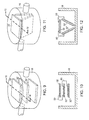
- more than one substrate 32 is disposed within the connection box 16 ( Figs. 9-12 ), and the serial electrical connection between respective interface conductors 42 of the different substrates 32, 32',32"... is achieved using jumpers 50 that extend between the respective interface conductors 42 ( Figs. 10, 12 ).
- the substrate sheets 32, 32', 32" when more than one substrate 32 is employed, the substrate sheets 32, 32', 32"... are disposed within the connection box 16 in a parallel, spaced apart arrangement ( Fig. 9, 10 ). In other embodiments, the substrate sheets 32 are arranged substantially edge to edge to form a polygon when viewed in section ( Fig. 11, 12 ).
- Interface conductors 42 are provided within the substrate 32, and are formed of superconductive material.
- the particular type of superconductive material employed to form the interface conductors 42 is determined by the specific requirements of the particular application.
- Examples of types of high temperature superconductors that may be used to form interface conductors 42 include, but are not limited to, copper oxide superconductors such as bismuth strontium calcium copper oxide (BSCCO), yttrium barium copper oxide (YBCO), and magnesium diboride (MgB 2 ).
- the interface conductors 42 will be formed of the same superconductive material that is used to form the HTS wires 3.
- the interface conductors 42 are disposed in the substrate 32 so as to extend from a first end 38 to a second end 40 of the substrate 32.
- the interface conductors 42 are deposited on the upper surface 34.
- the interface conductors 42 are laminated within the substrate, and include elongate exposed connection lands (connection points) 44 corresponding to each end of each interface conductor 42.
- the interface conductors 42 are arranged to extend in parallel within the substrate 32. Like the HTS flat wires 3, the interface conductors 42 are formed to have a generally rectangular cross section in which the interface conductor width w 1 is large relative to the conductor depth. The interface conductors 42 are oriented within the substrate 32 so that the conductor width is generally parallel to the upper surface 34 of the substrate 32.
- the interface conductor width w 1 is substantially the same as the width w 2 of the HTS wire 3.
- the interface conductor 42 may be formed of two, vertically stacked interface conductors 42a, 42b ( Fig. 7 ). By this arrangement, the current carrying capacity of the interface conductor is greater than that of the HTS wire 3. For example, by stacking two interface conductors 42a, 42b, the current carrying capacity of the interface conductor 42 is about twice the current carrying capacity of the HTS wire 3.
- an arrangement in which the interface conductor 42 is provided in a width w 1 that is much greater than, for example two times the width w 2 of the HTS wire 3, may be employed to achieve increased current carrying capacity ( Fig. 8 ).
- the interface conductors 42 are arranged within the substrate 32 in a way that joins respective ends 11, 19 of the HTS wire bundle 2 such that the individual HTS wires 3 are serially connected.
- An exemplary arrangement of interface conductors 42, including power supply lands 48, 49, is shown schematically in Fig. 13 , in which the interface conductors 42 are numbered from C1 to C13.
- the HTS wires 3 of one or more HTS wire bundles 2 may be received by the interface device 30.
- respective opposed ends of each HTS wire 3 are represented alphabetically, whereby both ends of a first HTS wire 3 are labeled "A”, both ends of another HTS wire 3 are labeled "B", et cetera, until each HTS wire 3 is uniquely represented.
- one or more HTS wire bundles 2 provide twelve HTS wires 3, represented as A, B, C, D, E, F, G, H, I, J, K, and L.
- a first end of the HTS wire A is connected to interface conductor C1 at the first end 38 of the substrate 32.
- interface conductor C1 corresponds to a power supply land 48, for example corresponding to a positive pole of the power supply 18.
- a first end of the HTS wire B is connected to interface conductor C2 at the first end 38 of the substrate 32
- a first end of the HTS wire C is connected to interface conductor C3 at the first end 38 of the substrate 32, and so forth.
- a second end of the HTS wire A is connected to interface conductor C2 at the second end 40 of the substrate 32.
- the connection location of the second end of the HTS wire 3 is offset by one interface conductor 42 relative to the connection location of its first end.
- a second end of the HTS wire B is connected to interface conductor C3 at the second end 40 of the substrate 32
- a second end of the HTS wire C is connected to interface conductor C4 at the second end 40 of the substrate 32 and so forth, continuing in this manner until the last HTS wire L is connected to interface conductor C13.
- interface conductor C13 corresponds to a power supply land 49, for example corresponding to a negative pole of the power supply 18.
- the interface device 30 is configured to receive opposed first and second ends 11, 19 of the HTS wire bundle 2, and to connect HTS wires 3 from the first end 11 to respective HTS wires 3 of the second end 19 to form at least one superconductive multi-turn winding.
- one or more HTS wire bundles 2 provide twelve HTS wires 3, and the interface device 30 has thirteen interface conductors 42. It is understood that the interface device 30 is not limited in the number of HTS wires that can be received. In particular, the interface device 30 is not limited to having thirteen interface conductors 42, but may be provided with greater or fewer numbers of interface conductors 42 as required by the specific application. For example, it is well within the art to provide one or more substrates 32 having interface conductors 42 as needed to accommodate the number of HTS wires 3 employed in a particular application.
- the interface device 30 For a junction box 14 configuration in which one or more HTS wire bundles 2 are connected to a single substrate 32, and the HTS wire bundles 2 comprise n HTS wires, then in order to form an electromagnetic winding employing all n of the HTS wires 3 of the HTS wire bundle 2, the interface device 30 must be provided with at least n+1 interface conductors 42 embedded in the substrate 32 such that at least n-1 interface conductors extend from the first end 38 to the second end 40.
- the first end 38 of the interface device 30 is connected to the first end 11 of the HTS wire bundle 2 such that the n i th interface conductor is joined to the n i th wire bundle conductor, and the second end of the interface device 40 is connected to the second end 19 of the HTS wire bundle 2 such that the n i th interface conductor is joined to the (n i +1)th wire bundle conductor.
- one end of the first interface conductor (n 1 ) is configured to accept power input
- one end of the (n+1) st interface conductor is configured to provide power output.
- the first end of the nth HTS wire 3 is connected to a first end of the nth interface conductor, and the second end of the nth HTS wire 3 is connected to the second end of the (n+1)th interface conductor.
- the interface device 30 is not limited to this particular sequence of connections.
- One of ordinary skill in the art is capable of determining other sequences of connections in which a multi-turn winding is obtained,
- connection box 16 may be configured to focus the flow of coolant 12 directly at the interface device 30. This can be achieved by providing an appropriate structure such as a nozzle (not shown) or deflector 17 ( Fig. 5 ) at the inlet of the coolant 12 to the connection box 16, or at a location intermediate the inlet and the interface device 30.
Landscapes
- Engineering & Computer Science (AREA)
- Power Engineering (AREA)
- Aviation & Aerospace Engineering (AREA)
- Superconductors And Manufacturing Methods Therefor (AREA)
- Containers, Films, And Cooling For Superconductive Devices (AREA)
Description
- The present invention relates to an electrical interface device for a degaussing system junction box.
- Lightweight conductors that can transmit large amounts of electric current without significant loss have numerous applications. For example, in electro-refining applications such as aluminum production processes, high amounts of current are required. Other applications requiring light-weight, high-current conductors are naval ships. Naval ships, typically formed of ferromagnetic materials and thus having a substantive magnetic field, are outfitted with complex degaussing systems which serve to reduce the magnetic field of the ship. This permits the naval ships to evade magnetic sensitive ordnances or devices such as mines that are triggered by the ship's large magnetic field.
- In a degaussing system, a system of electromagnetic windings ("degaussing coils") are provided within the ships hull. For example, multi-turn wire windings are installed to surround the ship hull in each of three orthogonal directions. By controlling the electric current flowing through the degaussing coils, the magnetic field generated by the ship's hull can be controlled and even "canceled". This, in turn, reduces the possibility of detection of the ship by magnetic sensitive ordnance or devices.
- To accommodate the high-current requirements in the exemplary applications described above, conventional wire cables, including degaussing coils, are formed of large diameter conductive wires, typically made of copper or aluminum wire. However, this leads to undesirably heavy, bulky, and inflexible cables.
- Recently, it has been proposed to replace the large diameter conventional cables with conductors formed of high-temperature superconducting (HTS) materials. As used herein, a high temperature superconductor (HTS) material refers to a material that can maintain superconducting behavior at temperatures of 20 K and higher (i.e., critical temperature, Tc ≥ 20 K). HTS wire bundles are disclosed in
WO 2008/011184 Accordingly, the HTS wire bundles afford greater flexibility, reduced weight, and high current carrying capacity, thereby having significant advantages over the conventional cables. - For both conventional cables and HTS wire bundles, in order to obtain a large wire winding using one or more multi-conductor cables/bundles, individual conductors within the multi-conductor cables or bundles must be serially joined. That is, an electromagnetic winding is formed from a multi-conductor cable or bundle by joining a first end of one conductor to the second end of another conductor, for each conductor until a single, multi-turn winding is obtained. For both conventional cables and HTS wire bundles, this is accomplished by manually soldering each connection, a process that is time consuming and highly labor intensive. Such soldering is prone to errors, including bad solder joints and improper connections, due to the difficulties associated with performing this work within the hull of a ship. Moreover, such errors are difficult to locate and repair.
- An apparatus for serially joining individual conductors of a multi-conductor superconductive wire bundle to form at least one multi-turn winding according to the present claim 1 is provided, comprising: an electrical interface device that serially joins individual high temperature superconductors (HTS) bundle conductors of a wire bundle to form at least one multi-turn superconductor winding, the interface device comprising: an input end, an output end. The apparatus is characterized in that it further comprises: a substrate, and a plurality of HTS interface conductors embedded in the substrate such that at least some of the interface conductors extend from the input end to the output end. The preferred embodiments are disclosed in the dependent claims.
- Modes for carrying out the present invention are explained below by reference to an embodiment of the present invention shown in the attached drawings. The above-mentioned object, other objects, characteristics and advantages of the present invention will become apparent form the detailed description of the embodiment of the invention presented below in conjunction with the attached drawings.
-
-
Fig. 1 is a schematic diagram of a degaussing system. -
Fig. 2 is a schematic diagram of a junction box. -
Fig. 3 is a cross sectional view of triad superstructure of HTS flat wires. -
Fig. 4 is a cross sectional view of a HTS wire bundle within a bundle cryostat. -
Fig. 5 is a schematic diagram of a connection box. -
Fig. 6 is a perspective view of a substrate. -
Fig. 7 is a partial perspective view of another embodiment of a substrate. -
Fig. 8 is a partial perspective view of still another embodiment of a substrate. -
Fig. 9 is a perspective view of substrates disposed the connection box. -
Fig. 10 is a sectional view along line 10-10 ofFig. 9 . -
Fig. 11 is a perspective view of substrates disposed in the connection box. -
Fig. 12 is a sectional view along line 12-12 ofFig. 11 . -
Fig. 13 is a view of the interface conductor configuration within the substrate. - Referring to
Fig. 1 , adegaussing system 10 is provided, which includes one or moreHTS wire bundles 2 enclosed in an elongate flexible bundle cryostat 4 (only a portion of thecryostat 4 is shown). The opposed ends of theHTS wire bundles 2 are received within ajunction box 14, which serves to consolidate the various systems needed to achieve degaussing. Arefrigeration unit 6 provides a suitable gas or liquid coolant 12 (e.g., cooled helium gas or liquid nitrogen) to an interior of aconnection box 16 provided within thejunction box 14, as well as to the bundle cryostat 4 via theconnection box 16. Apump 8 circulates thecoolant 12 from therefrigeration unit 6, through theconnection box 16 and through thebundle cryostat 4 to maintain the individualHTS wire conductors 3 within theHTS wire bundles 2 at a temperature at which superconduction is possible. In addition, power is supplied from apower supply 18 to the HTSwire bundle 2 via theconnection box 16. - In the
degaussing system 10 as shown, therefrigeration unit 6 and thepump 8 are shown as housed separately from thejunction box 14. However, thesystem 10 is not limited to this configuration. For example, in a more compact design, therefrigeration unit 6 andpump 8 may be integrated withinjunction box 14. - The
junction box 14, shown schematically inFig. 2 , is a cryostat and includes anouter housing 15 and an inner housing corresponding to theconnection box 16. The connection box (inner housing) 16 is substantially smaller in size than theouter housing 15 such that a relative largeintermediate space 24 is provided between theouter housing 15 and theconnection box 16. Theintermediate space 24 is vacated so that a vacuum exists in theintermediate space 24. In addition, a layer of insulation (not shown) may be provided on aninner surface 25 of theouter housing 15, or on anouter surface 27 of theinner housing 16. A supply ofcoolant 12 is provided to theinterior space 26 of theinner housing 16 by therefrigeration unit 6. - Referring again to
Fig. 1 , thejunction box 14 is configured to receive opposed first 11 and second 19 ends of one or more HTS wire bundles 2 (only one wire bundle is shown). TheHTS wire bundle 2 is formed ofmultiple HTS wires 3. In this particular embodiment, theHTS wire 3 is a "flat" wire, that is, theHTS wire 3 is formed to have a generally rectangular cross section in which the wire width is large relative to the wire depth, although theHTS wires 3 are not limited to this shape or proportion. The size of the cross-sectional area of the HTSflat wire 3 is related to the current carrying capacity of the wire such that an increase in the cross sectional area increases the current carrying capacity of the wire. The particular cross sectional area of theHTS wire 3 is determined by the specific requirements of the particular application. In addition, the particular type ofHTS wire 3 employed is also determined by the specific requirements of the particular application. Examples of types of high temperature superconductors that may be employed in theHTS wire bundle 2 include, but are not limited to, copper oxide superconductors such as bismuth strontium calcium copper oxide (BSCCO), yttrium barium copper oxide (YBCO), and magnesium diboride (MgB2). - In some embodiments, individual
flat wires 3 may be provided with a coating 5 of a compliant material prior to stacking. The coating material 5 may be a conductor, a semiconductor, or an insulator. For example, the coating material 5 may be Kapton® (registered trademark of E. I. du Pont de Nemours and Company) polyimide film. - In some embodiments, several HTS
flat wires 3 are arranged in astacked configuration 7, although the inventive concept described herein is not limited to a stacked configuration. As seen inFig. 3 , individual HTSflat wires 3 may be stacked so that adjacent HTSflat wires 3 may be slightly offset in the width direction. In this case, the resultingstack 7 has a cross-sectional shape that is a parallelogram such as a rhomboid. Thestack 7 is maintained in the desired configuration by any appropriate means, such as wrapping thestack 7 with polymer, paper, metal foil strip or the like (not shown). - In the illustrated embodiment, each
stack 7 is formed of eight HTSflat wires 3. However, the inventive concept described herein is not limited to this number, and eachstack 7 may be constituted by any number of HTSflat wires 3. In addition,several stacks 7 may be assembled together to form astack superstructure 9. In the illustrated embodiment, threestacks 7 of HTSflat wires 3 are assembled to form atriad superstructure 9 having a substantially hexagonally-shaped cross-section. However, any number ofstacks 7 may be assembled in any desired arrangement to form astack superstructure 9. The number ofstacks 7 employed and particular configuration of thestacks 7 is determined by the specific requirements of the particular application. - The
stack superstructure 9 is maintained in the desired configuration by any appropriate means. In some embodiments, thestack superstructure 9 is maintained in the desired configuration by providing thestack superstructure 9 with anoverwrap 21 formed of polymer tape or a preformed polymer helix such as a polytetraflouroethylene (TEFLON) wrap. As used herein, the termHTS wire bundle 2 refers to astack superstructure 9 surrounded by ahelical overwrap 21. - Each
HTS wire bundle 2 is elongate, and may range in length from a few meters to hundreds of meters. EachHTS wire bundle 2 includes opposed first 11 and second 19 wire bundle ends. The first and second wire bundle ends 11, 19 are received within thejunction box 14 such that each of the first and second wire bundle ends 11, 19 extend into theinterior space 26 of theconnection box 16. - At locations exterior of the
junction box 14, theHTS wire bundle 2 is disposed within the flexible bundle cryostat 4 (Fig. 4 ). Thebundle cryostat 4 is an assembly of elongate, coaxially arranged stainlesssteel tubular housings HTS wire bundle 2 is disposed within aninterior space 61 of theinner housing 62, and is supported within theinterior space 61 by one ormore support members 60. Anintermediate space 66 is provided between theinner housing 62 and theouter housing 64. Theintermediate space 66 is vacated so that a vacuum exists in theintermediate space 66. The length of thebundle cryostat 4 generally corresponds to the length of theHTS wire bundle 2, and thus can be in the range of a few meters to hundreds of meters. Thebundle cryostat 4 is joined to thejunction box 14 so that theinterior space 61 of theinner housing 62 opens to, and is in fluid communication with, theinterior space 26 of theconnection box 16.Fittings 67 are provided at respective opposed ends 63, 65 of thebundle cryostat 4 which permit thecoolant 12 to be injected under pressure into the openinterior space 61. Thecoolant 12, which flows between the respective opposed ends 63, 65 of thebundle cryostat 4, serves to maintain theHTS wires 3 at a temperature which permits theHTS wires 3, and thus theHTS wire bundle 2, to exhibit the property of superconductivity. In order to prevent thecoolant 12 from bypassing between the inlet and outlet of thebundle cryostat 4, aflow restrictor 13 can be placed in theHTS wire bundle 2. In some embodiments, thefittings 67 are configured to fix the ends 63, 65 of thebundle cryostat 4 to theouter housing 15. In other embodiments (not shown) thefittings 67 may fix the ends 63, 65 of thebundle cryostat 4 to theconnection box 16. - An
electrical interface device 30 is disposed in theinterior space 26 of the connection box 16 (Fig. 5 ). Theinterior space 26 receivescoolant 12 from therefrigeration unit 6, and thus is maintained at a sufficiently low temperature to permit superconductivity therewithin. Theinterface device 30 is a single entity that is configured to received each end of eachHTS wire 3 and superconductively connect theindividual HTS wires 3 in series, whereby one or more lengths of multi-conductorHTS wire bundle 2 are converted into a single, multi-turn degaussing winding. In this arrangement, each turn of the multi-turn winding is constituted by oneHTS wire 3. - In some embodiments, the interface device includes a
substrate 32 in whichseveral interface conductors 42 are provided (Fig. 6 ). Thesubstrate 32 may be formed of a conventional insulative material of the type used in printed circuit boards. For example, thesubstrate 32 may be formed of an epoxy resin, such as FR-4. The substrate is not limited to this material, and may be formed of other insulative material having properties which accommodate supporting electrical conductors in long term use at or below the critical temperature Tc found within theinterior space 26. - The
substrate 32 has anupper surface 34, and an opposedlower surface 36. Herein, directional references such as "upper" and "lower" are used to provide a relational description with reference to an orientation shown in the figures, and are not intended to be absolute or limiting. A thermally-conductive layer 46 is formed on thelower surface 36, and serves to conduct heat away frominterface conductors 42 disposed within thesubstrate 32. In some embodiments, the thermallyconductive layer 46 is formed of copper. -
Substrate 32 further includes power supply lands 48, 49 that permit connection of two of theinterface conductors 42 within theinterface device 30 to thepower supply 18. As discussed further below, when theindividual HTS wires 3 are connected to therespective interface conductors 42, power is supplied to theHTS wire bundle 2 from thepower supply 18 via the power supply lands 48, 49. Power supply lands 48, 49 may receive power frompower supply 18 via conventionalcopper wire conductors lands interface conductors 42, are formed of superconductive materials, and thus thelands power supply conductor HTS interface conductor 42. - In some embodiments, a
single substrate 32 is disposed within theconnection box 16. Thesubstrate 32 may be formed to be plate-like in shape, as shown inFig. 6 . In other embodiments, the substrate may be formed to provide a curved surface. Such a curved surface may be C-shaped, circular, or spiral shaped when viewed in cross-section. - In other embodiments, more than one
substrate 32 is disposed within the connection box 16 (Figs. 9-12 ), and the serial electrical connection betweenrespective interface conductors 42 of thedifferent substrates jumpers 50 that extend between the respective interface conductors 42 (Figs. 10, 12 ). - In some embodiments, when more than one
substrate 32 is employed, thesubstrate sheets connection box 16 in a parallel, spaced apart arrangement (Fig. 9, 10 ). In other embodiments, thesubstrate sheets 32 are arranged substantially edge to edge to form a polygon when viewed in section (Fig. 11, 12 ). -
Interface conductors 42 are provided within thesubstrate 32, and are formed of superconductive material. The particular type of superconductive material employed to form theinterface conductors 42 is determined by the specific requirements of the particular application. Examples of types of high temperature superconductors that may be used to forminterface conductors 42 include, but are not limited to, copper oxide superconductors such as bismuth strontium calcium copper oxide (BSCCO), yttrium barium copper oxide (YBCO), and magnesium diboride (MgB2). In some embodiments, theinterface conductors 42 will be formed of the same superconductive material that is used to form theHTS wires 3. - As seen in
Fig. 6 , theinterface conductors 42 are disposed in thesubstrate 32 so as to extend from afirst end 38 to asecond end 40 of thesubstrate 32. In some embodiments, theinterface conductors 42 are deposited on theupper surface 34. In other embodiments, theinterface conductors 42 are laminated within the substrate, and include elongate exposed connection lands (connection points) 44 corresponding to each end of eachinterface conductor 42. - The
interface conductors 42 are arranged to extend in parallel within thesubstrate 32. Like the HTSflat wires 3, theinterface conductors 42 are formed to have a generally rectangular cross section in which the interface conductor width w1 is large relative to the conductor depth. Theinterface conductors 42 are oriented within thesubstrate 32 so that the conductor width is generally parallel to theupper surface 34 of thesubstrate 32. - In some embodiments, the interface conductor width w1 is substantially the same as the width w2 of the
HTS wire 3. In other embodiments, in order to provide more current carrying capacity, theinterface conductor 42 may be formed of two, vertically stackedinterface conductors Fig. 7 ). By this arrangement, the current carrying capacity of the interface conductor is greater than that of theHTS wire 3. For example, by stacking twointerface conductors interface conductor 42 is about twice the current carrying capacity of theHTS wire 3. Alternatively, an arrangement in which theinterface conductor 42 is provided in a width w1 that is much greater than, for example two times the width w2 of theHTS wire 3, may be employed to achieve increased current carrying capacity (Fig. 8 ). - Moreover, the
interface conductors 42 are arranged within thesubstrate 32 in a way that joins respective ends 11, 19 of theHTS wire bundle 2 such that theindividual HTS wires 3 are serially connected. An exemplary arrangement ofinterface conductors 42, including power supply lands 48, 49, is shown schematically inFig. 13 , in which theinterface conductors 42 are numbered from C1 to C13. - The
HTS wires 3 of one or more HTS wire bundles 2 may be received by theinterface device 30. In this example, respective opposed ends of eachHTS wire 3 are represented alphabetically, whereby both ends of afirst HTS wire 3 are labeled "A", both ends of anotherHTS wire 3 are labeled "B", et cetera, until eachHTS wire 3 is uniquely represented. In this example, one or more HTS wire bundles 2 provide twelveHTS wires 3, represented as A, B, C, D, E, F, G, H, I, J, K, and L. - In the illustrated example of
Fig. 13 , a first end of the HTS wire A is connected to interface conductor C1 at thefirst end 38 of thesubstrate 32. In this case, interface conductor C1 corresponds to apower supply land 48, for example corresponding to a positive pole of thepower supply 18. Similarly, a first end of the HTS wire B is connected to interface conductor C2 at thefirst end 38 of thesubstrate 32, a first end of the HTS wire C is connected to interface conductor C3 at thefirst end 38 of thesubstrate 32, and so forth. - Also in the illustrated example, a second end of the HTS wire A is connected to interface conductor C2 at the
second end 40 of thesubstrate 32. Thus, the connection location of the second end of theHTS wire 3 is offset by oneinterface conductor 42 relative to the connection location of its first end. Similarly, a second end of the HTS wire B is connected to interface conductor C3 at thesecond end 40 of thesubstrate 32, a second end of the HTS wire C is connected to interface conductor C4 at thesecond end 40 of thesubstrate 32 and so forth, continuing in this manner until the last HTS wire L is connected to interface conductor C13. In this case, interface conductor C13 corresponds to apower supply land 49, for example corresponding to a negative pole of thepower supply 18. By this arrangement, theinterface device 30 is configured to receive opposed first and second ends 11, 19 of theHTS wire bundle 2, and to connectHTS wires 3 from thefirst end 11 torespective HTS wires 3 of thesecond end 19 to form at least one superconductive multi-turn winding. - In the illustrated example of
Fig. 13 , one or more HTS wire bundles 2 provide twelveHTS wires 3, and theinterface device 30 has thirteeninterface conductors 42. It is understood that theinterface device 30 is not limited in the number of HTS wires that can be received. In particular, theinterface device 30 is not limited to having thirteeninterface conductors 42, but may be provided with greater or fewer numbers ofinterface conductors 42 as required by the specific application. For example, it is well within the art to provide one ormore substrates 32 havinginterface conductors 42 as needed to accommodate the number ofHTS wires 3 employed in a particular application. - For a
junction box 14 configuration in which one or more HTS wire bundles 2 are connected to asingle substrate 32, and the HTS wire bundles 2 comprise n HTS wires, then in order to form an electromagnetic winding employing all n of theHTS wires 3 of theHTS wire bundle 2, theinterface device 30 must be provided with at least n+1interface conductors 42 embedded in thesubstrate 32 such that at least n-1 interface conductors extend from thefirst end 38 to thesecond end 40. Thefirst end 38 of theinterface device 30 is connected to thefirst end 11 of theHTS wire bundle 2 such that the nith interface conductor is joined to the nith wire bundle conductor, and the second end of theinterface device 40 is connected to thesecond end 19 of theHTS wire bundle 2 such that the nith interface conductor is joined to the (ni+1)th wire bundle conductor. In this configuration, one end of the first interface conductor (n1) is configured to accept power input, and one end of the (n+1)st interface conductor is configured to provide power output. - In the illustrated example of
Fig. 13 , the first end of thenth HTS wire 3 is connected to a first end of the nth interface conductor, and the second end of thenth HTS wire 3 is connected to the second end of the (n+1)th interface conductor. However, theinterface device 30 is not limited to this particular sequence of connections. One of ordinary skill in the art is capable of determining other sequences of connections in which a multi-turn winding is obtained, - As described above,
coolant 12 is directed into theconnection box 16 to maintain theinterface device 30 and theHTS wires 3 within thebundle cryostat 4 at a temperature which permits theHTS wires 3 and theinterface conductors 42 to exhibit the property of superconductivity. In some embodiments, theconnection box 16 may be configured to focus the flow ofcoolant 12 directly at theinterface device 30. This can be achieved by providing an appropriate structure such as a nozzle (not shown) or deflector 17 (Fig. 5 ) at the inlet of thecoolant 12 to theconnection box 16, or at a location intermediate the inlet and theinterface device 30. - A selected illustrative embodiment of the invention is described above in some detail. It should be understood that only structures considered necessary for clarifying the present invention have been described herein. Other conventional structures, and those of ancillary and auxiliary components of the system, are assumed to be known and understood by those skilled in the art. Moreover, while a working example of the present invention has been described above, the present invention is not limited to the working example described above, but various design alterations may be carried out without departing from the present invention as set forth in the claims.
Claims (14)
- An apparatus for serially joining individual conductors of a multi- conductor superconductive wire bundle (2) to form at least one multi-turn winding, comprising:an electrical interface device (30) that serially joins individual high temperature superconductors (HTS) bundle conductors (3) of a wire bundle to form at least one multi-turn superconductor winding, the interface device comprising: an input end, an output end;the apparatus characterized in that it further comprises: a substrate (32), anda plurality of HTS interface conductors (42) embedded in the substrate (32) such that at least some of the interface conductors extend from the input end to the output end.
- The apparatus of claim 1, further comprising:at least one high temperature superconductor (HTS) wire bundle (2), each HTS wire bundle including multiple HTS bundle conductors (3), each bundle conductor having opposed first (11) and second (19) bundle conductor ends,a housing (16),an electrical interface device (30) disposed in the housing, the interface device configured to receive each end of each bundle conductor of each HTS wire bundle,wherein the interface device is configured to electrically connect respective first end of bundle conductors to respective second ends of other bundle conductors to form at least one multi-turn winding.
- The apparatus of claim 2, wherein the interface device (30) is configured to provide a superconductive electrical connection of the respective first ends (11) of bundle conductors to the respective second ends (19) of other bundle conductors to form at least one multi-turn superconducting winding.
- The apparatus of claim 2, wherein the housing (16) defines a cryostat.
- The apparatus of claim 1, wherein the electrical interface device (30) comprises: a substrate (32), and
a plurality of interface conductors (42) formed of a superconductive material, the interface conductors disposed in the substrate. - The apparatus of claim 5,
wherein the substrate (32) is formed into a sheet (32, 32', 32") having a first side, and a second side opposed to the first side,
wherein the plurality of interface conductors (42) extends within the substrate (30) such that at least a portion of the connection lands (44) corresponding to each end of each interface conductor are exposed on the first side of the substrate; and
wherein a layer (46) of thermally conductive material is provided on the second side of the substrate (32). - The apparatus of claim 2, wherein
the at least one wire bundle (2) comprises a wire bundle having n conductors, and
the electrical interface device (30) comprises:an input end,an output end,a substrate (32); andn+1 interface conductors (42) embedded in the substrate (32) such that atleast n-1 interface conductors extend from the input end to the output end,wherein
one of the input end and the output end of the interface device is connected to the first end (11) of the wire bundle such that the nith interface conductor is joined to the nith wire bundle conductor, and the other of the input end and the output end of the interface device (30) is connected to the second end (19) of the wire bundle such that the nith interface conductor is joined to the (n i+1)th wire bundle conductor. - The apparatus of claim 1, wherein the electrical interface device (30) comprises:a plurality of substrates (32, 32', 32"), each substrate including a plurality of interface conductors (42) formed of a superconductive material, the interface conductors disposed in the respective substrate.
- The apparatus of claim 1, wherein
one of the input end and the output end of the interface device (30) is connected to the first end (11) of the wire bundle such that an nth interface conductor is joined to an nth bundle conductor, and
the other of the input end and the output end of the electrical interface device is connected to the second end (19) of the wire bundle such that the nth HTS interface conductor is joined to the (n+1)th bundle conductor. - The apparatus of claim 1,
wherein the substrate (32) is formed into a sheet having a first side, and a second side opposed to the first side, and
wherein the plurality of HTS interface conductors (42) extends within the substrate such that at least a portion of the connection lands (44) corresponding to each end of each HTS interface conductor are exposed on the first side of the substrate. - The apparatus of claim 1, further comprising a layer (46) of thermally conductive material provided on a side of the substrate (32).
- The apparatus of claim 1,
wherein an individual HTS interface conductor (42) has a first current carrying capacity, wherein
an individual HTS bundle conductor (3) has a second current capacity, and wherein said first current carrying capacity is greater than said second current carrying capacity. - The apparatus of claim 1, wherein the electrical interface device (30) comprises plural substrates.
- The apparatus of claim 1, wherein
a first end (11) of one HTS interface conductor is configured to connect to an input conductor of a power supply, and a second end (19) of the one HTS interface conductor corresponds to the input end of the interface device, and
a first end of an other interface HTS conductor is configured to connect to an output conductor of a power supply, and a second end of the other HTS interface conductor corresponds to the output end of the interface device.
Applications Claiming Priority (2)
| Application Number | Priority Date | Filing Date | Title |
|---|---|---|---|
| US12/057,836 US8731629B2 (en) | 2008-03-28 | 2008-03-28 | Interface device for a high temperature superconductor degaussing system junction box |
| PCT/US2009/037524 WO2009120553A1 (en) | 2008-03-28 | 2009-03-18 | Interface device and junction box for a htsc degaussing coil |
Publications (2)
| Publication Number | Publication Date |
|---|---|
| EP2257953A1 EP2257953A1 (en) | 2010-12-08 |
| EP2257953B1 true EP2257953B1 (en) | 2014-11-19 |
Family
ID=40690773
Family Applications (1)
| Application Number | Title | Priority Date | Filing Date |
|---|---|---|---|
| EP09725012.0A Active EP2257953B1 (en) | 2008-03-28 | 2009-03-18 | Interface device and junction box for a htsc degaussing coil |
Country Status (7)
| Country | Link |
|---|---|
| US (1) | US8731629B2 (en) |
| EP (1) | EP2257953B1 (en) |
| KR (1) | KR101330233B1 (en) |
| AU (1) | AU2009228535B2 (en) |
| CA (1) | CA2719469C (en) |
| ES (1) | ES2528296T3 (en) |
| WO (1) | WO2009120553A1 (en) |
Families Citing this family (9)
| Publication number | Priority date | Publication date | Assignee | Title |
|---|---|---|---|---|
| DE4426753A1 (en) * | 1994-07-28 | 1996-02-01 | Bayer Ag | Means for controlling plant pests |
| US8731629B2 (en) | 2008-03-28 | 2014-05-20 | American Superconductor Corporation | Interface device for a high temperature superconductor degaussing system junction box |
| KR100957623B1 (en) * | 2009-10-30 | 2010-05-13 | 한국전력공사 | Ac loss measurement device of high temperature superconductor |
| US9093200B2 (en) | 2013-07-09 | 2015-07-28 | Advanced Conductor Technologies Llc | Multiphase coaxial superconducting cables and corc degaussing system |
| EP2919325B1 (en) * | 2014-03-11 | 2017-02-22 | Nexans | End terminator for a supra-conducting electric cable |
| KR20180105181A (en) | 2016-01-21 | 2018-09-27 | 브룩해븐 테크놀로지 그룹, 인크. | Second generation superconducting filaments and cables |
| US10811589B2 (en) | 2016-09-07 | 2020-10-20 | Brookhaven Technology Group, Inc. | Reel-to-reel exfoliation and processing of second generation superconductors |
| WO2018227083A1 (en) | 2017-06-09 | 2018-12-13 | Brookhaven Technology Group, Inc. | Flexible multi-filament high temperature superconducting cable |
| GB2574210B (en) * | 2018-05-30 | 2022-09-28 | Siemens Healthcare Ltd | Superconducting joints |
Family Cites Families (7)
| Publication number | Priority date | Publication date | Assignee | Title |
|---|---|---|---|---|
| DE2205045A1 (en) | 1972-02-03 | 1973-08-09 | Wilhelm Dr Ing Lepper | COILS FOR DC OR AC |
| JPS62234880A (en) * | 1986-04-04 | 1987-10-15 | 株式会社日立製作所 | Method of jointing superconducting wire |
| DE3905424C2 (en) | 1989-02-22 | 1994-02-17 | Vacuumschmelze Gmbh | Process for producing a superconducting connection between oxide superconductors |
| JP2003123866A (en) | 2001-10-15 | 2003-04-25 | Mitsubishi Heavy Ind Ltd | Connection structure of superconducting wire |
| US7608785B2 (en) * | 2004-04-27 | 2009-10-27 | Superpower, Inc. | System for transmitting current including magnetically decoupled superconducting conductors |
| JP5431932B2 (en) * | 2006-07-21 | 2014-03-05 | アメリカン スーパーコンダクター コーポレイション | High current small flexible conductor containing high temperature superconducting tape |
| US8731629B2 (en) | 2008-03-28 | 2014-05-20 | American Superconductor Corporation | Interface device for a high temperature superconductor degaussing system junction box |
-
2008
- 2008-03-28 US US12/057,836 patent/US8731629B2/en active Active
-
2009
- 2009-03-18 CA CA2719469A patent/CA2719469C/en active Active
- 2009-03-18 KR KR1020107023902A patent/KR101330233B1/en active IP Right Grant
- 2009-03-18 EP EP09725012.0A patent/EP2257953B1/en active Active
- 2009-03-18 ES ES09725012.0T patent/ES2528296T3/en active Active
- 2009-03-18 AU AU2009228535A patent/AU2009228535B2/en active Active
- 2009-03-18 WO PCT/US2009/037524 patent/WO2009120553A1/en active Application Filing
Also Published As
| Publication number | Publication date |
|---|---|
| AU2009228535B2 (en) | 2013-05-16 |
| EP2257953A1 (en) | 2010-12-08 |
| KR101330233B1 (en) | 2013-11-15 |
| CA2719469A1 (en) | 2009-10-01 |
| ES2528296T3 (en) | 2015-02-06 |
| WO2009120553A1 (en) | 2009-10-01 |
| US20090247411A1 (en) | 2009-10-01 |
| KR20100127297A (en) | 2010-12-03 |
| US8731629B2 (en) | 2014-05-20 |
| AU2009228535A1 (en) | 2009-10-01 |
| CA2719469C (en) | 2015-05-19 |
Similar Documents
| Publication | Publication Date | Title |
|---|---|---|
| EP2257953B1 (en) | Interface device and junction box for a htsc degaussing coil | |
| US10943712B2 (en) | Superconducting cables and methods of making the same | |
| US6512311B1 (en) | High power superconducting cable | |
| EP2050104B1 (en) | High-current, compact flexible conductors containing high temperature superconducting tapes | |
| JP5663127B2 (en) | System for transmitting current including magnetically separated superconducting conductors | |
| EP0623937B1 (en) | High-Tc superconducting cable conductor employing oxide superconductor | |
| US7151225B2 (en) | Superconducting cable and superconducting cable line using the same | |
| US11394263B2 (en) | Superconductive electric coil device and rotor comprising a coil device | |
| WO2000039813A1 (en) | Superconducting cable | |
| WO2007080794A1 (en) | Superconducting cable | |
| US11488747B2 (en) | Superconducting power cable system | |
| EP2447957A2 (en) | Superconducting cable system | |
| KR102580374B1 (en) | Hybrid joint assembly of low temperature superconducting conduit conductor and high temperature superconducting conduit conductor, hybrid joint method low temperature superconducting conduit conductor and high temperature superconducting conduit conductor, and extension method of low temperature superconducting conduit conductor and high temperature superconducting conduit conductor therefor | |
| Wang et al. | Design and Development of a Large Superconducting Solenoid with Aluminum-Stabilized Superconductors |
Legal Events
| Date | Code | Title | Description |
|---|---|---|---|
| PUAI | Public reference made under article 153(3) epc to a published international application that has entered the european phase |
Free format text: ORIGINAL CODE: 0009012 |
|
| 17P | Request for examination filed |
Effective date: 20100902 |
|
| AK | Designated contracting states |
Kind code of ref document: A1 Designated state(s): AT BE BG CH CY CZ DE DK EE ES FI FR GB GR HR HU IE IS IT LI LT LU LV MC MK MT NL NO PL PT RO SE SI SK TR |
|
| AX | Request for extension of the european patent |
Extension state: AL BA RS |
|
| DAX | Request for extension of the european patent (deleted) | ||
| 17Q | First examination report despatched |
Effective date: 20131219 |
|
| RIC1 | Information provided on ipc code assigned before grant |
Ipc: H01F 6/06 20060101ALI20140410BHEP Ipc: B63G 9/06 20060101AFI20140410BHEP Ipc: H01F 13/00 20060101ALN20140410BHEP |
|
| REG | Reference to a national code |
Ref country code: DE Ref legal event code: R079 Ref document number: 602009027846 Country of ref document: DE Free format text: PREVIOUS MAIN CLASS: H01F0006060000 Ipc: B63G0009060000 |
|
| GRAP | Despatch of communication of intention to grant a patent |
Free format text: ORIGINAL CODE: EPIDOSNIGR1 |
|
| INTG | Intention to grant announced |
Effective date: 20140606 |
|
| RIC1 | Information provided on ipc code assigned before grant |
Ipc: H01F 13/00 20060101ALN20140526BHEP Ipc: H01F 6/06 20060101ALI20140526BHEP Ipc: B63G 9/06 20060101AFI20140526BHEP |
|
| GRAS | Grant fee paid |
Free format text: ORIGINAL CODE: EPIDOSNIGR3 |
|
| GRAA | (expected) grant |
Free format text: ORIGINAL CODE: 0009210 |
|
| AK | Designated contracting states |
Kind code of ref document: B1 Designated state(s): AT BE BG CH CY CZ DE DK EE ES FI FR GB GR HR HU IE IS IT LI LT LU LV MC MK MT NL NO PL PT RO SE SI SK TR |
|
| REG | Reference to a national code |
Ref country code: GB Ref legal event code: FG4D |
|
| REG | Reference to a national code |
Ref country code: CH Ref legal event code: EP |
|
| REG | Reference to a national code |
Ref country code: AT Ref legal event code: REF Ref document number: 696828 Country of ref document: AT Kind code of ref document: T Effective date: 20141215 |
|
| REG | Reference to a national code |
Ref country code: IE Ref legal event code: FG4D |
|
| REG | Reference to a national code |
Ref country code: DE Ref legal event code: R096 Ref document number: 602009027846 Country of ref document: DE Effective date: 20141231 |
|
| REG | Reference to a national code |
Ref country code: ES Ref legal event code: FG2A Ref document number: 2528296 Country of ref document: ES Kind code of ref document: T3 Effective date: 20150206 |
|
| REG | Reference to a national code |
Ref country code: NL Ref legal event code: T3 |
|
| REG | Reference to a national code |
Ref country code: AT Ref legal event code: MK05 Ref document number: 696828 Country of ref document: AT Kind code of ref document: T Effective date: 20141119 |
|
| REG | Reference to a national code |
Ref country code: GR Ref legal event code: EP Ref document number: 20150400337 Country of ref document: GR Effective date: 20150318 |
|
| REG | Reference to a national code |
Ref country code: LT Ref legal event code: MG4D |
|
| PG25 | Lapsed in a contracting state [announced via postgrant information from national office to epo] |
Ref country code: FI Free format text: LAPSE BECAUSE OF FAILURE TO SUBMIT A TRANSLATION OF THE DESCRIPTION OR TO PAY THE FEE WITHIN THE PRESCRIBED TIME-LIMIT Effective date: 20141119 Ref country code: PT Free format text: LAPSE BECAUSE OF FAILURE TO SUBMIT A TRANSLATION OF THE DESCRIPTION OR TO PAY THE FEE WITHIN THE PRESCRIBED TIME-LIMIT Effective date: 20150319 Ref country code: NO Free format text: LAPSE BECAUSE OF FAILURE TO SUBMIT A TRANSLATION OF THE DESCRIPTION OR TO PAY THE FEE WITHIN THE PRESCRIBED TIME-LIMIT Effective date: 20150219 Ref country code: LT Free format text: LAPSE BECAUSE OF FAILURE TO SUBMIT A TRANSLATION OF THE DESCRIPTION OR TO PAY THE FEE WITHIN THE PRESCRIBED TIME-LIMIT Effective date: 20141119 Ref country code: IS Free format text: LAPSE BECAUSE OF FAILURE TO SUBMIT A TRANSLATION OF THE DESCRIPTION OR TO PAY THE FEE WITHIN THE PRESCRIBED TIME-LIMIT Effective date: 20150319 |
|
| PG25 | Lapsed in a contracting state [announced via postgrant information from national office to epo] |
Ref country code: AT Free format text: LAPSE BECAUSE OF FAILURE TO SUBMIT A TRANSLATION OF THE DESCRIPTION OR TO PAY THE FEE WITHIN THE PRESCRIBED TIME-LIMIT Effective date: 20141119 Ref country code: LV Free format text: LAPSE BECAUSE OF FAILURE TO SUBMIT A TRANSLATION OF THE DESCRIPTION OR TO PAY THE FEE WITHIN THE PRESCRIBED TIME-LIMIT Effective date: 20141119 Ref country code: CY Free format text: LAPSE BECAUSE OF FAILURE TO SUBMIT A TRANSLATION OF THE DESCRIPTION OR TO PAY THE FEE WITHIN THE PRESCRIBED TIME-LIMIT Effective date: 20141119 Ref country code: PL Free format text: LAPSE BECAUSE OF FAILURE TO SUBMIT A TRANSLATION OF THE DESCRIPTION OR TO PAY THE FEE WITHIN THE PRESCRIBED TIME-LIMIT Effective date: 20141119 Ref country code: SE Free format text: LAPSE BECAUSE OF FAILURE TO SUBMIT A TRANSLATION OF THE DESCRIPTION OR TO PAY THE FEE WITHIN THE PRESCRIBED TIME-LIMIT Effective date: 20141119 Ref country code: HR Free format text: LAPSE BECAUSE OF FAILURE TO SUBMIT A TRANSLATION OF THE DESCRIPTION OR TO PAY THE FEE WITHIN THE PRESCRIBED TIME-LIMIT Effective date: 20141119 |
|
| PG25 | Lapsed in a contracting state [announced via postgrant information from national office to epo] |
Ref country code: CZ Free format text: LAPSE BECAUSE OF FAILURE TO SUBMIT A TRANSLATION OF THE DESCRIPTION OR TO PAY THE FEE WITHIN THE PRESCRIBED TIME-LIMIT Effective date: 20141119 Ref country code: RO Free format text: LAPSE BECAUSE OF FAILURE TO SUBMIT A TRANSLATION OF THE DESCRIPTION OR TO PAY THE FEE WITHIN THE PRESCRIBED TIME-LIMIT Effective date: 20141119 Ref country code: EE Free format text: LAPSE BECAUSE OF FAILURE TO SUBMIT A TRANSLATION OF THE DESCRIPTION OR TO PAY THE FEE WITHIN THE PRESCRIBED TIME-LIMIT Effective date: 20141119 Ref country code: SK Free format text: LAPSE BECAUSE OF FAILURE TO SUBMIT A TRANSLATION OF THE DESCRIPTION OR TO PAY THE FEE WITHIN THE PRESCRIBED TIME-LIMIT Effective date: 20141119 Ref country code: DK Free format text: LAPSE BECAUSE OF FAILURE TO SUBMIT A TRANSLATION OF THE DESCRIPTION OR TO PAY THE FEE WITHIN THE PRESCRIBED TIME-LIMIT Effective date: 20141119 |
|
| REG | Reference to a national code |
Ref country code: DE Ref legal event code: R097 Ref document number: 602009027846 Country of ref document: DE |
|
| PLBE | No opposition filed within time limit |
Free format text: ORIGINAL CODE: 0009261 |
|
| STAA | Information on the status of an ep patent application or granted ep patent |
Free format text: STATUS: NO OPPOSITION FILED WITHIN TIME LIMIT |
|
| 26N | No opposition filed |
Effective date: 20150820 |
|
| PG25 | Lapsed in a contracting state [announced via postgrant information from national office to epo] |
Ref country code: MC Free format text: LAPSE BECAUSE OF FAILURE TO SUBMIT A TRANSLATION OF THE DESCRIPTION OR TO PAY THE FEE WITHIN THE PRESCRIBED TIME-LIMIT Effective date: 20141119 Ref country code: LU Free format text: LAPSE BECAUSE OF FAILURE TO SUBMIT A TRANSLATION OF THE DESCRIPTION OR TO PAY THE FEE WITHIN THE PRESCRIBED TIME-LIMIT Effective date: 20150318 |
|
| REG | Reference to a national code |
Ref country code: CH Ref legal event code: PL |
|
| REG | Reference to a national code |
Ref country code: IE Ref legal event code: MM4A |
|
| PG25 | Lapsed in a contracting state [announced via postgrant information from national office to epo] |
Ref country code: CH Free format text: LAPSE BECAUSE OF NON-PAYMENT OF DUE FEES Effective date: 20150331 Ref country code: LI Free format text: LAPSE BECAUSE OF NON-PAYMENT OF DUE FEES Effective date: 20150331 Ref country code: IE Free format text: LAPSE BECAUSE OF NON-PAYMENT OF DUE FEES Effective date: 20150318 |
|
| PG25 | Lapsed in a contracting state [announced via postgrant information from national office to epo] |
Ref country code: SI Free format text: LAPSE BECAUSE OF FAILURE TO SUBMIT A TRANSLATION OF THE DESCRIPTION OR TO PAY THE FEE WITHIN THE PRESCRIBED TIME-LIMIT Effective date: 20141119 |
|
| REG | Reference to a national code |
Ref country code: FR Ref legal event code: PLFP Year of fee payment: 8 |
|
| PG25 | Lapsed in a contracting state [announced via postgrant information from national office to epo] |
Ref country code: MT Free format text: LAPSE BECAUSE OF FAILURE TO SUBMIT A TRANSLATION OF THE DESCRIPTION OR TO PAY THE FEE WITHIN THE PRESCRIBED TIME-LIMIT Effective date: 20141119 |
|
| REG | Reference to a national code |
Ref country code: FR Ref legal event code: PLFP Year of fee payment: 9 |
|
| PG25 | Lapsed in a contracting state [announced via postgrant information from national office to epo] |
Ref country code: BG Free format text: LAPSE BECAUSE OF FAILURE TO SUBMIT A TRANSLATION OF THE DESCRIPTION OR TO PAY THE FEE WITHIN THE PRESCRIBED TIME-LIMIT Effective date: 20141119 Ref country code: HU Free format text: LAPSE BECAUSE OF FAILURE TO SUBMIT A TRANSLATION OF THE DESCRIPTION OR TO PAY THE FEE WITHIN THE PRESCRIBED TIME-LIMIT; INVALID AB INITIO Effective date: 20090318 |
|
| PG25 | Lapsed in a contracting state [announced via postgrant information from national office to epo] |
Ref country code: BE Free format text: LAPSE BECAUSE OF FAILURE TO SUBMIT A TRANSLATION OF THE DESCRIPTION OR TO PAY THE FEE WITHIN THE PRESCRIBED TIME-LIMIT Effective date: 20141119 |
|
| REG | Reference to a national code |
Ref country code: FR Ref legal event code: PLFP Year of fee payment: 10 |
|
| PG25 | Lapsed in a contracting state [announced via postgrant information from national office to epo] |
Ref country code: MK Free format text: LAPSE BECAUSE OF FAILURE TO SUBMIT A TRANSLATION OF THE DESCRIPTION OR TO PAY THE FEE WITHIN THE PRESCRIBED TIME-LIMIT Effective date: 20141119 |
|
| PGFP | Annual fee paid to national office [announced via postgrant information from national office to epo] |
Ref country code: GR Payment date: 20200330 Year of fee payment: 12 Ref country code: IT Payment date: 20200323 Year of fee payment: 12 Ref country code: NL Payment date: 20200326 Year of fee payment: 12 |
|
| PGFP | Annual fee paid to national office [announced via postgrant information from national office to epo] |
Ref country code: TR Payment date: 20200303 Year of fee payment: 12 |
|
| PGFP | Annual fee paid to national office [announced via postgrant information from national office to epo] |
Ref country code: ES Payment date: 20200401 Year of fee payment: 12 |
|
| REG | Reference to a national code |
Ref country code: NL Ref legal event code: MM Effective date: 20210401 |
|
| PG25 | Lapsed in a contracting state [announced via postgrant information from national office to epo] |
Ref country code: NL Free format text: LAPSE BECAUSE OF NON-PAYMENT OF DUE FEES Effective date: 20210401 |
|
| PG25 | Lapsed in a contracting state [announced via postgrant information from national office to epo] |
Ref country code: GR Free format text: LAPSE BECAUSE OF NON-PAYMENT OF DUE FEES Effective date: 20211008 |
|
| PG25 | Lapsed in a contracting state [announced via postgrant information from national office to epo] |
Ref country code: IT Free format text: LAPSE BECAUSE OF NON-PAYMENT OF DUE FEES Effective date: 20210318 |
|
| REG | Reference to a national code |
Ref country code: ES Ref legal event code: FD2A Effective date: 20220523 |
|
| PG25 | Lapsed in a contracting state [announced via postgrant information from national office to epo] |
Ref country code: TR Free format text: LAPSE BECAUSE OF NON-PAYMENT OF DUE FEES Effective date: 20210318 |
|
| PG25 | Lapsed in a contracting state [announced via postgrant information from national office to epo] |
Ref country code: ES Free format text: LAPSE BECAUSE OF NON-PAYMENT OF DUE FEES Effective date: 20210319 |
|
| PGFP | Annual fee paid to national office [announced via postgrant information from national office to epo] |
Ref country code: FR Payment date: 20230327 Year of fee payment: 15 |
|
| P01 | Opt-out of the competence of the unified patent court (upc) registered |
Effective date: 20230810 |
|
| PGFP | Annual fee paid to national office [announced via postgrant information from national office to epo] |
Ref country code: DE Payment date: 20240327 Year of fee payment: 16 Ref country code: GB Payment date: 20240327 Year of fee payment: 16 |