EP2255239B1 - Image sensor and focus detection apparatus - Google Patents
Image sensor and focus detection apparatus Download PDFInfo
- Publication number
- EP2255239B1 EP2255239B1 EP09719788.3A EP09719788A EP2255239B1 EP 2255239 B1 EP2255239 B1 EP 2255239B1 EP 09719788 A EP09719788 A EP 09719788A EP 2255239 B1 EP2255239 B1 EP 2255239B1
- Authority
- EP
- European Patent Office
- Prior art keywords
- focus detection
- pixels
- image
- pixel
- lattice
- Prior art date
- Legal status (The legal status is an assumption and is not a legal conclusion. Google has not performed a legal analysis and makes no representation as to the accuracy of the status listed.)
- Active
Links
- 238000001514 detection method Methods 0.000 title claims description 376
- 210000001747 pupil Anatomy 0.000 claims description 104
- 230000003287 optical effect Effects 0.000 claims description 62
- 238000004364 calculation method Methods 0.000 claims description 15
- 238000000034 method Methods 0.000 description 42
- 238000003384 imaging method Methods 0.000 description 39
- 239000011295 pitch Substances 0.000 description 30
- 238000009826 distribution Methods 0.000 description 24
- 230000000694 effects Effects 0.000 description 17
- 238000006243 chemical reaction Methods 0.000 description 16
- 238000005070 sampling Methods 0.000 description 16
- 230000008569 process Effects 0.000 description 11
- 238000009825 accumulation Methods 0.000 description 10
- 230000006870 function Effects 0.000 description 10
- 238000012546 transfer Methods 0.000 description 10
- 239000003990 capacitor Substances 0.000 description 9
- 230000015556 catabolic process Effects 0.000 description 8
- 230000002950 deficient Effects 0.000 description 8
- 238000006731 degradation reaction Methods 0.000 description 8
- 230000000875 corresponding effect Effects 0.000 description 6
- 230000007423 decrease Effects 0.000 description 5
- 230000003247 decreasing effect Effects 0.000 description 5
- 238000012545 processing Methods 0.000 description 5
- 230000008878 coupling Effects 0.000 description 4
- 238000010168 coupling process Methods 0.000 description 4
- 238000005859 coupling reaction Methods 0.000 description 4
- 230000002093 peripheral effect Effects 0.000 description 4
- 238000002360 preparation method Methods 0.000 description 4
- 238000012937 correction Methods 0.000 description 3
- 238000011156 evaluation Methods 0.000 description 3
- 238000005286 illumination Methods 0.000 description 3
- 238000012986 modification Methods 0.000 description 3
- 230000004048 modification Effects 0.000 description 3
- 229910021420 polycrystalline silicon Inorganic materials 0.000 description 3
- 230000035945 sensitivity Effects 0.000 description 3
- 101001005389 Homo sapiens Protein LTV1 homolog Proteins 0.000 description 2
- 102100025932 Protein LTV1 homolog Human genes 0.000 description 2
- 230000001154 acute effect Effects 0.000 description 2
- 239000000969 carrier Substances 0.000 description 2
- 230000008859 change Effects 0.000 description 2
- 230000001276 controlling effect Effects 0.000 description 2
- 238000010586 diagram Methods 0.000 description 2
- 238000007689 inspection Methods 0.000 description 2
- 230000011514 reflex Effects 0.000 description 2
- 230000004044 response Effects 0.000 description 2
- 230000003595 spectral effect Effects 0.000 description 2
- 230000004075 alteration Effects 0.000 description 1
- 238000003705 background correction Methods 0.000 description 1
- 230000008901 benefit Effects 0.000 description 1
- 238000004891 communication Methods 0.000 description 1
- 230000006835 compression Effects 0.000 description 1
- 238000007906 compression Methods 0.000 description 1
- 238000012790 confirmation Methods 0.000 description 1
- 238000007796 conventional method Methods 0.000 description 1
- 230000002596 correlated effect Effects 0.000 description 1
- 230000003111 delayed effect Effects 0.000 description 1
- 238000009792 diffusion process Methods 0.000 description 1
- 238000007429 general method Methods 0.000 description 1
- 239000000203 mixture Substances 0.000 description 1
- 238000012544 monitoring process Methods 0.000 description 1
- 230000002265 prevention Effects 0.000 description 1
- 230000009467 reduction Effects 0.000 description 1
- 238000000926 separation method Methods 0.000 description 1
- 229910052709 silver Inorganic materials 0.000 description 1
- 239000004332 silver Substances 0.000 description 1
- -1 silver halide Chemical class 0.000 description 1
- 230000007480 spreading Effects 0.000 description 1
- 230000002194 synthesizing effect Effects 0.000 description 1
- 230000000007 visual effect Effects 0.000 description 1
- 229910052724 xenon Inorganic materials 0.000 description 1
- FHNFHKCVQCLJFQ-UHFFFAOYSA-N xenon atom Chemical compound [Xe] FHNFHKCVQCLJFQ-UHFFFAOYSA-N 0.000 description 1
Images


Classifications
-
- G—PHYSICS
- G02—OPTICS
- G02B—OPTICAL ELEMENTS, SYSTEMS OR APPARATUS
- G02B7/00—Mountings, adjusting means, or light-tight connections, for optical elements
- G02B7/28—Systems for automatic generation of focusing signals
- G02B7/34—Systems for automatic generation of focusing signals using different areas in a pupil plane
- G02B7/346—Systems for automatic generation of focusing signals using different areas in a pupil plane using horizontal and vertical areas in the pupil plane, i.e. wide area autofocusing
-
- G—PHYSICS
- G03—PHOTOGRAPHY; CINEMATOGRAPHY; ANALOGOUS TECHNIQUES USING WAVES OTHER THAN OPTICAL WAVES; ELECTROGRAPHY; HOLOGRAPHY
- G03B—APPARATUS OR ARRANGEMENTS FOR TAKING PHOTOGRAPHS OR FOR PROJECTING OR VIEWING THEM; APPARATUS OR ARRANGEMENTS EMPLOYING ANALOGOUS TECHNIQUES USING WAVES OTHER THAN OPTICAL WAVES; ACCESSORIES THEREFOR
- G03B13/00—Viewfinders; Focusing aids for cameras; Means for focusing for cameras; Autofocus systems for cameras
- G03B13/32—Means for focusing
- G03B13/34—Power focusing
- G03B13/36—Autofocus systems
-
- H—ELECTRICITY
- H04—ELECTRIC COMMUNICATION TECHNIQUE
- H04N—PICTORIAL COMMUNICATION, e.g. TELEVISION
- H04N2101/00—Still video cameras
Definitions
- the present invention relates to an image sensor capable of sensing at least either still images or moving images using many two-dimensionally arrayed photoelectric conversion elements, and a method of detecting a focus state in an image sensing apparatus using the image sensor.
- a contrast detection method (called a blur detection method) and a phase difference detection method (called a defocus detection method) have been proposed as general methods using a light beam having passed through an imaging optical system in automatic focus detection/adjustment of an image sensing apparatus.
- the contrast detection method is often used in a video movie camera (camcorder) for recording a moving image, and an electronic still camera.
- the image sensor is used as a focus detection sensor.
- This method pays attention to the output signal of the image sensor, especially high-frequency component information (contrast information), and a position of the imaging optical system where the evaluation value maximizes is set as an in-focus position.
- this contrast detection method also called a hill-climbing detection method, is not suitable for a high-speed focus adjustment operation because the evaluation value is obtained while slightly moving the imaging optical system, and the imaging optical system needs to be moved until it is determined that the evaluation value was maximum.
- the phase difference detection method is generally adopted in single-lens reflex cameras using a silver halide film, and is a technique most contributed to practical use of AF (Auto Focus) single-lens reflex cameras.
- AF Auto Focus
- a light beam having passed through the exit pupil of the imaging optical system is split into two, and the two light beams are received by a pair of focus detection sensors.
- the defocus amount of the imaging optical system in the focusing direction is directly obtained by detecting the difference between signals output in accordance with the light reception amounts, that is, the relative positional error amount in the direction in which the light beam is split.
- the focus detection sensor executes the accumulation operation, the defocus amount and direction can be attained to perform a high-speed focus adjustment operation.
- an optical path division means such as a quick return mirror or half-mirror is generally inserted in the image sensing optical path, and a focus detection optical system and AF sensor are arranged on the output side of the optical path division means.
- the pupil division function is added to some light receiving elements (pixels) of an image sensor by decentering the sensitive areas of their light receiving portions from the optical axis of an on-chip microlens.
- These pixels are used as focus detection pixels, and arranged between image sensing pixels at predetermined intervals to perform phase difference focus detection. Since no image sensing pixel exists at portions where focus detection pixels are arranged, image information is generated by interpolation using information from peripheral image sensing pixels.
- the pupil division function is implemented by dividing each of the light receiving portions of some pixels of an image sensor into two, right and left, or upper and lower portions. These pixels are used as focus detection pixels, and arranged between image sensing pixels at predetermined intervals to perform phase difference focus detection. According to this technique as well, no image sensing pixel exists at portions where focus detection pixels are arranged, so image information is generated by interpolation using information from peripheral image sensing pixels.
- the pupil division function is provided by dividing each of the light receiving portions of some pixels of an image sensor into two, upper and lower portions. Outputs from the two divided light receiving portions are individually processed to execute phase difference focus detection for an object having a luminance distribution in the vertical direction. Outputs from the two divided light receiving portions are added and used as an image sensing signal. Further, the contrast between pixels adjacent to each other in the horizontal direction is detected to perform contrast focus detection for an object having a luminance distribution in the horizontal direction.
- focus detection elements whose light receiving portions are divided into right and left, or upper and lower portions are repetitively arranged every other line of an image sensor. With this arrangement, phase difference focus detection is done for an object having luminance distributions in the horizontal and vertical directions.
- focus detection pixels When generating an output image, focus detection pixels function as singular or defective pixels. To prevent degradation of an output image, the following items need to be satisfied.
- US 2007/206940 discloses a focus adjustment device includes focus detection pixels for detecting a focus adjustment state of an imaging optical system through a first pupil division-type image shift detection method, a focus detector that detects a focus adjustment state at the imaging optical system through a second pupil division-type image shift detection method different from the first pupil division-type image shift detection method.
- the present invention has been made to overcome the conventional drawbacks, and has as its object to enable detection of phase differences in two directions at an arbitrary position in a predetermined unit area of an image sensing unit, and detecting the focus of even an object having contrast information in only one direction.
- an image sensor as claimed in claim 1 herein.
- Figs. 1 to 22 are views according to the first preferred embodiment of the present invention. The first embodiment will be explained with reference to these drawings.
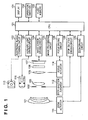
- Fig. 1 is a view of the arrangement of a camera according to the preferred embodiment of the present invention.
- Fig. 1 shows an electronic camera configured by integrating a camera body having an image sensor serving as an image sensing unit, and an imaging optical system.
- a first lens group 101 is arranged on the first stage of the imaging optical system (image forming optical system), and is held reciprocally along the optical axis.
- a stop/shutter 102 adjusts the aperture diameter to adjust the light quantity in shooting.
- the stop/shutter 102 also functions as a shutter for adjusting the exposure time when sensing a still image.
- the stop/shutter 102 and a second lens group 103 reciprocate together along the optical axis to achieve a zooming operation (zooming function) in synchronism with the reciprocal operation of the first lens group 101.
- a third lens group 105 reciprocates along the optical axis to adjust the focus.
- An optical lowpass filter 106 is an optical element for reducing the false color and moire of a sensed image.
- An image sensor 107 includes a C-MOS sensor and its peripheral circuit. The image sensor is a two-dimensional 1CCD color sensor in which a primary color mosaic filter with the Bayer array is formed on a chip of m light receiving pixels in the horizontal direction and n light receiving pixels in the vertical direction.
- a zoom actuator 111 drives the first lens group 101 to third lens group 105 to reciprocate along the optical axis and perform the zooming operation.
- a stop/shutter actuator 1,12 controls the aperture diameter of the stop/shutter 102 to adjust the light quantity in shooting, and controls the exposure time when sensing a still image.
- a focus actuator 114 drives the third lens group 105 to reciprocate along the optical axis and adjust the focus.
- An electronic flash 115 is used to illuminate an object in shooting.
- the electronic flash 115 is preferably a flash illumination device using a xenon tube, but may also be an illumination device having a continuous emission LED.
- An AF auxiliary light unit 116 projects, to the field via a projection lens, an image of a mask having a predetermined aperture pattern, and improves the focus detection capability for a dark object or low-contrast object.
- a CPU 121 in the camera executes various control operations of the camera body.
- the CPU 121 includes, for example, an arithmetic unit, ROM, RAM, A/D converter, D/A converter, communication interface circuit, and the like. Based on a predetermined program stored in the ROM, the CPU 121 drives various circuits of the camera to execute a series of operations such as AF, shooting, image processing, and recording.
- An electronic flash control circuit 122 controls the ON operation of the electronic flash 115 in synchronism with the shooting operation.
- An auxiliary light driving circuit 123 controls the ON operation of the AF auxiliary light unit 116 in synchronism with a focus detection operation of detecting the focus state of the image forming optical system.
- An image sensor driving circuit 124 controls the image sensing operation of the image sensor 107, A/D-converts an acquired image signal, and transmits the digital data to the CPU 121.
- An image processing circuit 125 performs processes such as ⁇ conversion, color interpolation, and JPEG compression for an image obtained by the image sensor 107.
- a focus driving circuit 126 controls to drive the focus actuator 114 on the basis of the focus detection result, and drives the third lens group 105 to reciprocate along the optical axis, thereby adjusting the focus.
- a stop/shutter driving circuit 128 controls to drive the stop/shutter actuator 112, thereby controlling the aperture of the stop/shutter 102.
- a zoom driving circuit 129 drives the zoom actuator 111 in accordance with the zooming operation of the user.
- a display 131 is, for example, an LCD, and displays information on the shooting mode of the camera, a preview image before shooting, a confirmation image after shooting, an in-focus display image upon focus detection, and the like.
- Operation switches 132 include a power switch, release (shooting trigger) switch, zooming operation switch, shooting mode selection switch, and the like.
- a detachable flash memory 133 records a sensed image.
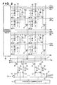
- Fig. 2 is a schematic circuit diagram of the image sensor according to the preferred embodiment of the present invention.
- the image sensor is manufactured according to a technique disclosed in, for example, Japanese Patent Laid-Open No. 09-046596 filed by the present inventor.
- Fig. 2 shows a pixel area of two columns ⁇ four rows in a two-dimensional C-MOS area sensor. When the area sensor is used as an image sensor, many pixels each shown in Fig. 2 are arranged to be able to obtain a high-resolution image.
- a photoelectric conversion portion 1 of a photoelectric conversion element is formed from a MOS transistor gate and a depletion layer below the gate.
- Reference numeral 2 denotes a photogate; and 3, a transfer switch MOS transistor.
- Reference numeral 4 denotes a reset MOS transistor; 5, a source follower amplifier MOS transistor; 6, a horizontal selection switch MOS transistor; and 7, a source follower load MOS transistor.
- Reference numeral 8 denotes a dark output transfer MOS transistor; 9, a bright output transfer MOS transistor; 10, a dark output accumulation capacitor C TN ; 11, a bright output accumulation capacitor C TS ; and 12, a horizontal transfer MOS transistor.
- Reference numeral 13 denotes a horizontal output line reset MOS transistor; 14, a differential output amplifier; 15, a horizontal scanning circuit; and 16, a vertical scanning circuit.
- Fig. 3 is a sectional view of a pixel portion.
- reference numeral 17 denotes a P-well; 18, a gate oxide film; 19, a first poly-Si layer; 20, a second poly-Si layer; and 21, an n + -floating diffusion (FD).
- the FD 21 is connected to another photoelectric conversion portion via another transfer MOS transistor.
- the drain of two transfer MOS transistors 3 and the FD 21 are shared to increase the sensitivity by micropatterning and reduction in the capacity of the FD 21.
- the FD 21 may also be connected by, for example, an Al wire.
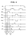
- This timing chart shows a case wherein signals are independently output from all pixels.
- a control pulse ⁇ L changes to high level to reset a vertical output line.
- Control pulses ⁇ R 0 , ⁇ PG 00 , and ⁇ PG e0 change to high level to turn on the reset MOS transistor 4 and set the first poly-Si layer 19 of the photogate 2 to high level.
- a control pulse ⁇ S 0 changes to high level to turn on the selection switch MOS transistor 6 and select pixels on the first and second lines.
- the control pulse ⁇ R 0 changes to low level to stop resetting the FD 21 and set it to the floating state. Charges pass through the gate-source path of the source follower amplifier MOS transistor 5.
- a control pulse ⁇ T N changes to high level to output the dark voltage of the FD 21 to the accumulation capacitor C TN 10 by the source follower operation.
- a control pulse ⁇ TX 00 for the first line changes to high level to turn on the transfer switch MOS transistor 3.
- the control pulse ⁇ PG 00 changes to low level.
- the potential well spreading below the photogate 2 rises to completely transfer photoinduced carriers to the FD 21.
- the control pulse ⁇ TX need not be a pulse and may also be a fixed potential as long as carriers can be completely transferred.
- the potential of the FD 21 changes depending on light. Since the source follower amplifier MOS transistor 5 floats, the potential of the FD 21 is output to the accumulation capacitor C TS 11 by changing a control pulse ⁇ T s to high level in the time T 3 . Up to this time, dark and bright outputs from pixels on the first line have been accumulated in the accumulation capacitors C TN 10 and C TS 11, respectively. In the time T 4 , a control pulse ⁇ HC temporarily changes to high level to turn on the horizontal output line reset MOS transistors 13 and reset the horizontal output lines.
- the differential output V OUT is obtained within the chip.
- a conventional CDS (Correlated Double Sampling) circuit arranged outside the chip, in place of obtaining the differential output V OUT within the chip.
- the control pulse ⁇ R 0 changes to high level to turn on the reset MOS transistor 4 and reset the FD 21 to the power supply V DD .
- photocharges are read out from the second line.
- the control pulses ⁇ TX e0 and ⁇ PG e0 are similarly driven, and the high-level control pulses ⁇ T N and ⁇ T s are supplied to accumulate photocharges in the accumulation capacitors C TN 10 and C TS 11, and output dark and bright outputs. By this driving, photocharges can be independently read out from the first and second lines.
- the control pulses ⁇ T N and ⁇ TX 01 change to high level, the control pulse ⁇ PG 01 changes to low level, the control pulse ⁇ T s changes to high level, and the control pulse ⁇ HC temporarily changes to high level, thereby reading out pixel signals from pixels 30-31 and 30-32.
- the control pulses ⁇ TX e1 and ⁇ PG e1 are applied in the above-described way, reading out pixel signals from pixels 30-41 and 30-42.
- Figs. 5A, 5B , 6A, 6B , 7A, and 7B are views for explaining the structure of an image sensing pixel and that of a focus detection pixel serving as a focus detection unit.
- Figs. 5A and 5B show the arrangement and structure of image sensing pixels.
- Fig. 5A is a plan view of 2 ⁇ 2 image sensing pixels.
- G pixels are diagonally arranged, and R and B pixels are arranged as the two remaining pixels. This 2 ⁇ 2 structure is repetitively arranged.
- Fig. 5B is a sectional view taken along the line A - A in Fig. 5A .
- Reference symbol ML denotes an on-chip microlens arranged in front of each pixel; CF R , an R (Red) color filter; and CF G , a G (Green) color filter.
- Reference symbol PD Photo Diode denotes a schematic photoelectric conversion portion of the C-MOS sensor shown in Fig. 3 .
- Reference symbol CL (Contact Layer) denotes an interconnection layer for forming a signal line for transmitting various signals within the C-MOS sensor.
- Reference symbol TL Taking Lens denotes a schematic imaging optical system.
- the on-chip microlens ML and photoelectric conversion portion PD of the image sensing pixel are configured to capture a light beam having passed through the imaging optical system TL as effectively as possible.
- an exit pupil EP (Exit Pupil) of the imaging optical system TL and the photoelectric conversion portion PD are conjugate to each other via the microlens ML, and the effective area of the photoelectric conversion portion is designed so as to be large.
- Fig. 5B shows a light beam entering the R pixel, but the G pixel and B (Blue) pixel also have the same structure.
- the exit pupil EP corresponding to each of R, G, and B image sensing pixels has a large diameter, and a light beam (light quantum) from an object can be efficiently captured to increase the S/N ratio of an image signal.
- Figs. 6A and 6B show the arrangement and structure of focus detection pixels (first focus detection pixels) for dividing the pupil in the horizontal direction (lateral direction) of the imaging optical system.
- the horizontal direction or lateral direction is defined as a direction along a straight line which is perpendicular to the optical axis and extends horizontally when the user holds the camera so that the optical axis of the imaging optical system becomes parallel to the horizontal direction.
- Fig. 6A is a plan view of 2 ⁇ 2 pixels including focus detection pixels.
- the main component of luminance information is obtained by G pixels.
- the image recognition features of humans are sensitive to luminance information. Thus, if G pixels are omitted, degradation of the image quality is readily perceived.
- R or B pixels are used to acquire color information (color difference information).
- the visual features of humans are not sensitive to color information. Hence, even if pixels for acquiring color information are slightly omitted, degradation of the image quality is hardly recognized. From this, in the embodiment, G pixels out of 2 ⁇ 2 pixels are left as image sensing pixels, and R and B pixels are replaced with focus detection pixels. In Fig. 6A , S HA and S HB represent focus detection pixels.
- Fig. 6B is a sectional view taken along the line A - A in Fig. 6A .
- the microlens ML and photoelectric conversion portion PD have the same structures as those of the image sensing pixel shown in Fig. 5B .
- a signal from the focus detection pixel is not used to generate an image, so a transparent film CF W (White) is arranged in place of a color filter for color separation.
- the aperture of the interconnection layer CL deviates in one direction from the center line of the microlens ML.
- an aperture OP HA of the pixel S HA deviates to the right and receives a light beam having passed through a left exit pupil EP HA of the imaging optical system TL.
- an aperture OP HB of the pixel S HB deviates to the left and receives a light beam having passed through a right exit pupil EP HB of the imaging optical system TL.
- Pixels S HA are arrayed regularly in the horizontal direction, and an object image obtained by these pixels is defined as image A.
- Pixels S HB are also arrayed regularly in the horizontal direction, and an object image obtained by these pixels is defined as image B.
- the pixels S HA and S HB can detect the focus of an object, for example, a vertical line having a luminance distribution in the lateral direction of the photographing frame, but cannot detect the focus of a horizontal line having a luminance distribution in the longitudinal direction.
- the embodiment adopts a pixel for dividing the pupil even in the vertical direction (longitudinal direction) of the imaging optical system.
- Figs. 7A and 7B show the arrangement and structure of focus detection pixels (second focus detection pixels) for dividing the pupil in the vertical direction (in other words, the top-to-bottom direction or longitudinal direction) of the imaging optical system.
- the vertical direction, top-to-bottom direction, or longitudinal direction is defined as a direction along a straight line which is perpendicular to the optical axis and extends vertically when the user holds the camera so that the optical axis of the imaging optical system becomes parallel to the horizontal direction.
- Fig. 7A is a plan view of 2 ⁇ 2 pixels including focus detection pixels. Similar to Fig. 6A , G pixels are left as image sensing pixels, and R and B pixels are replaced with focus detection pixels.
- S VC and S VD represent focus detection pixels.
- Fig. 7B is a sectional view taken along the line A - A in Fig. 7A .
- the pixel in Fig. 7B has the same structure as that in Fig. 6B except that the pixel in Fig. 6B has a structure for dividing the pupil in the lateral direction, but the pixel in Fig. 7B has a structure for dividing the pupil in the longitudinal direction.
- an aperture OP VC of the pixel S VC deviates down and receives a light beam having passed through an upper exit pupil EP VC of the imaging optical system TL.
- an aperture OP VD of the pixel S VD deviates up and receives a light beam having passed through a lower exit pupil EP VD of the imaging optical system TL.
- Pixels S VC are arrayed regularly in the vertical direction, and an object image obtained by these pixels is defined as image C.
- Pixels S VD are also arrayed regularly in the vertical direction, and an object image obtained by these pixels is defined as image D.
- Figs. 8 to 10 are views for explaining arrangement rules for image sensing pixels and focus detection pixels shown in Figs. 5A, 5B , 6A, 6B , 7A, and 7B .
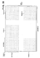
- Fig. 8 is a view for explaining an arrangement rule for a minimum unit when discretely arranging focus detection pixels between image sensing pixels.
- 10 rows ⁇ 10 columns 100 pixels are defined as one block.
- an upper left block BLK(1,1) the bottom left R and B pixels are replaced with a pair of focus detection pixels S HA and S HA for dividing the pupil in the horizontal direction.
- a block BLK(1,2) on the right side of the block BLK(1,1) the bottom left R and B pixels are similarly replaced with a pair of focus detection pixels S VC and S VD for dividing the pupil in the vertical direction.
- a block BLK(2,1) below the first block BLK(1,1) has the same pixel array as that of the block BLK(1,2).
- a block BLK(2,2) on the right side of the block BLK(2,1) has the same pixel array as that of the first block BLK(1,1).
- a focus detection pixel for horizontal pupil division is arranged in a block BLK(i,j) when i+j is an even number, and a focus detection pixel for vertical pupil division is arranged in it when i+j is an odd number.
- Phase difference detection characteristics in two directions can be made equal to each other by alternately arranging focus detection pixels for horizontal pupil division and focus detection pixels for vertical pupil division in the above-described way.
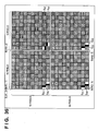
- Fig. 9 is a view for explaining an arrangement rule for the cluster serving as a unit.
- the bottom left R and B pixels of each block are replaced with focus detection pixels S HA and S HA or S VC and S VD .
- focus detection pixels in each block are arranged at positions shifted up by two pixels from those in the cluster CST(1,1).
- focus detection pixels in each block are arranged at positions shifted to the right by two pixels from those in the cluster CST(1,1). This rule is repetitively applied to obtain the arrangement shown in Fig. 9 .
- the coordinates of a focus detection pixel are defined by those of an upper left pixel in a set of four pixels including G pixels shown in Fig. 6A or 7A .
- the coordinates of the upper left corner of each block are defined as (1,1), and coordinates are incremented in the down and right directions.
- the horizontal coordinate of a focus detection pixel pair in each block of a cluster CST(u,w) is 2 ⁇ u-1, and the vertical coordinate is 11-2 ⁇ w.
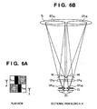
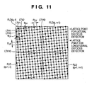
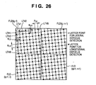
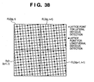
- Fig. 10 is a view for explaining an arrangement rule for the field serving as a unit.
- all fields FLD(q,r) have the same array as that of the first field FLD(1,1).
- the symbol o represents a point where the first focus detection pixel group for dividing the exit pupil of the imaging optical system in the lateral direction (right-to-left direction or horizontal direction) is arranged.
- the first focus detection pixel group is a pair of two pixels S HA and S HB in Fig. 6A , and the barycenter of the two pixels exists at o in Fig. 11 .
- the symbol ⁇ represents a point where the second focus detection pixel group for dividing the pupil in the longitudinal direction (up-to-bottom direction or vertical direction) is arranged.
- the symbol ⁇ corresponds to the barycenter of the two pixels S VC and S VD in Fig. 7A .
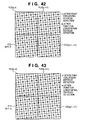
- LTH1 to LTH10 form a first lattice line group of lattice lines each formed by linking o in the lateral direction.
- a direction (first direction) in which the first lattice line group extends is inclined counterclockwise by ⁇ LH from a horizontal line. This angle will be called a horizontal argument, and the sign is positive in the counterclockwise direction.
- the absolute value of the horizontal argument is desirably as small as possible. This is because the relative position of a pair of images acquired by pixels for horizontally dividing the pupil is shifted in the horizontal direction in proportion to the defocus amount of the imaging optical system, and pixels for sampling the image are also preferably arranged along the relative shift direction of the image.
- focus detection pixels are arranged to form the first lattice line group horizontally, effects unique to the embodiment, which will be explained with reference to Fig. 12 and subsequent drawings, cannot be obtained. For this reason, the inclination angle of +5.7° is applied. If the arrangement rule described with reference to Fig. 9 changes, the inclination angle also changes, but is desirably double or less the angle in the embodiment, that is, less than or equal to about ⁇ 12°.
- a lattice pitch P LH which is the arrangement interval between adjacent lattice lines of the first lattice line group, is 10 (pixels).
- the lattice pitch decreases, the sampling density of a focus detection image increases to reduce a sampling error, but the number of omitted pixels in an output image increases.
- the optimum value of the lattice pitch should be determined in consideration of the balance between the image quality and the focus detection capability in an image sensing system. Studies made by the present applicant reveal that the lattice pitch is preferably selected from the range of 4 to 20 pixels.
- LTV1 to LTV10 form a second lattice line group of lattice lines each formed by linking ⁇ in the vertical direction (second direction).
- a direction in which the second lattice line group extends is also inclined from a vertical line.
- This inclination angle will be called a vertical argument, and the sign is positive in the counterclockwise direction.
- This inclination angle is also desirably as small as possible because of the same reason as that for the first lattice line group.
- the relative position of a pair of images acquired by pixels for vertically dividing the pupil is shifted in the vertical direction in proportion to the defocus amount of the imaging optical system, and pixels for sampling the images are also preferably arranged along the shift direction of the images.
- the vertical argument of the second lattice line group is also desirably double or less the angle in the embodiment, that is, less than or equal to about ⁇ 12°.
- a lattice pitch P LV which is the arrangement interval between adjacent lattice lines of the second lattice line group, is also 10 (pixels), and the setting rule is the same as that for the first lattice line group.
- the first lattice line group is formed from parallel lines (straight lines) which extend in a direction almost coincident with the first pupil division direction and are arranged equally at predetermined pitches.
- the second lattice line group is formed from parallel lines which extend in a direction almost coincident with the second pupil division direction and are arranged equally at predetermined pitches.
- the two lattice line groups cross each other perpendicularly (at an angle of 90°). to form a 2-dimensional lattice.
- Focus detection pixels are periodically arranged near the intersections (lattice points). In this manner, the moving direction of a focus detection image in a defocused state and the array direction of focus detection pixels substantially coincide with each other.
- Focus detection pixels are arranged "near" lattice points because two focus detection pixels are paired and replace R and B pixels in most embodiments of the present invention, and it is impossible to always arrange the pixels strictly on one lattice point.
- the effects of the present invention can be maintained even if the pixel arrangement position slightly shifts from a strict lattice point. Studies made by the present applicant reveal that the deviation of a pixel group from a lattice point is preferably less than or equal to 0.25 of the lattice pitch or less than or equal to four times or less of the image sensing pixel pitch.
- the first and second lattice line groups cross each other perpendicularly (at an angle of 90°).
- the present invention includes even a case wherein the crossing angle slightly differs from the right angle (90°), as long as the effects of the present invention can be obtained.
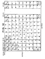
- FIG. 12 is a view for explaining a pixel grouping method when detecting the lateral defocus of an object image formed by the imaging optical system.
- phase difference focus detection is performed using focus detection pixels for dividing the exit pupil of the imaging optical system in the lateral direction (right-to-left direction or horizontal direction) described with reference to Figs. 6A and 6B .
- the pixel array shown in Fig. 12 is the same as that shown in Fig. 9 .
- One focus detection area is defined as an AF area.
- One section includes five pixels S HA corresponding to one divided pupil in the lateral direction, and five pixels S HB corresponding to the other divided pupil.
- outputs from the five pixels S HA are added to obtain one AF pixel of one image signal (called image A) for calculating the phase difference.
- outputs from the five pixels S HB are added to obtain one AF pixel of the other image signal (called image B) for calculating the phase difference.
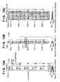
- Figs. 13A to 13C are views for explaining the object image capturing capability of one section.
- Fig. 13A shows a leftmost section SCT h (1) cut out from Fig. 12 .
- a horizontal line PRJ h shown at the bottom of Fig. 13A is the first projection line extending in the pupil division direction of the focus detection pixels S HA and S HB .
- a vertical line PRJ v shown on the right side of Fig. 13A is the second projection line extending in a direction perpendicular to the pupil division direction. Signals from all pixels S HA in one section are added, and those from all pixels S HB are also added.
- the AF pixel according to the embodiment has the same arrangement pitches in the pupil division direction and the direction perpendicular to it.
- the group shape in grouping is designed to be a rectangle to reduce a sampling error in the pupil division direction. More specifically, the maximum size L1 of one section in the pupil division direction is 10 pixels, and the maximum size L2 in the direction perpendicular to the pupil division direction is 100 pixels. By setting the section sizes to L1 ⁇ L2, the sampling frequency F1 in the pupil division direction is set high (dense), and the sampling frequency F2 in the direction perpendicular to it is set low (sparse).
- LINE v represents a thin vertical line projected on the image sensor 107, and has a width of four pixels in pixel conversion and 8 ⁇ m in the actual size of an image.
- focus detection pixels in the blocks BLK(3,1) and BLK(5,1) of the section SCT h (1) capture the object image.
- the minimum size of an object image is determined by the aberration of the imaging optical system and the characteristics of the optical LPF arranged in front of the image sensor. In general, even a very thin line has a width of two or more pixels.
- At least one pixel S HA and one pixel S HB capture an image, preventing a capturing failure.
- Fig. 13B it can be detected that the thin line LINE v exists in the section. However, the barycenter position of the thin line in the pupil division direction in the section cannot be detected.
- LINE h in Fig. 13B represents a thin horizontal line projected on the image sensor 107, and has a width of four pixels in pixel conversion and 8 ⁇ m in the actual size of an image, similar to the thin vertical line LINE v .
- the horizontal line LINE h is projected on the block BLK(5,1), but is not captured by the focus detection pixels S HA and S HB .
- the section SCT h (1) is used to detect the focus of an object having a luminance distribution in the lateral direction, like a vertical line. Thus, it does not matter if no focus detection pixel captures the image of an object having a luminance distribution in the longitudinal direction, like a horizontal line.
- Fig. 13C shows a case wherein a thick line BAND v wider than the thin line LINE v shown in Fig. 13B is formed over a plurality of sections.
- four pairs of focus detection pixels in the left section SCT h (1) capture the thick line BAND v .
- Five pairs of focus detection pixels in the center section SCT h (2) capture the thick line BAND v , and one pair of focus detection pixels in the right section SCT h (3) captures it.
- the barycenter position of the thick line BAND v can be detected at a resolution higher than the size L1 of each section in the pupil division direction.
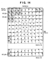
- Fig. 14 is a view for explaining a pixel grouping method when detecting the longitudinal defocus of an object image formed by the imaging optical system.
- phase difference focus detection is performed using focus detection pixels for dividing the exit pupil of the imaging optical system in the longitudinal direction (top-to-bottom direction or vertical direction) described with reference to Figs. 7A and 7B .
- the arrangement in Fig. 14 corresponds to one obtained by rotating the arrangement shown in Fig. 12 through 90°.
- the pixel array shown in Fig. 14 is also the same as that shown in Fig. 9 .
- One focus detection area is also defined as an AF area, similar to Fig. 12 .
- One section includes five pixels S VC corresponding to one divided pupil in the longitudinal direction, and five pixels S VD corresponding to the other divided pupil.
- outputs from the five pixels S VC are added to obtain one AF pixel of one image signal (called image C) for calculating the phase difference.
- outputs from the five pixels S VD are added to obtain one AF pixel of the other image signal (called image D) for calculating the phase difference.
- Figs. 15A to 15C are views for explaining the object image capturing capability of one section.
- the method in Figs. 15A to 15C is equivalent to one obtained by rotating the method in Figs. 13A to 13C through 90°.
- Fig. 15A shows a top section cut out from Fig. 14 .
- a vertical line PRJ v shown on the right side of Fig. 15A is the third projection line extending in the pupil division direction of the focus detection pixels Svc and S VD .
- a horizontal line PRJ h shown at the bottom of Fig. 15A is the fourth projection line extending in the direction perpendicular to the pupil division direction.
- signals from all pixels Svc in one section are added, and those from all pixels S VD are also added.
- the sampling characteristic of the AF pixel in Figs. 15A to 15C is F1 > F2, similar to the characteristic shown in Figs. 13A to 13C .
- LINE h represents a thin horizontal line projected on the image sensor 107, and has a width of four pixels in pixel conversion and 8 ⁇ m in the actual size of an image.
- focus detection pixels in the blocks BLK(1,4) and BLK(1,6) of the section SCT v (1) capture the object image.
- LINE v in Fig. 15B represents a thin vertical line projected on the image sensor 107, and has a width of four pixels in pixel conversion and 8 ⁇ m in the actual size of an image, similar to the thin horizontal line LINE h .
- the vertical line LINE v is projected on the block BLK(1,6), but is not captured by the focus detection pixels S VC and S VD .
- the section SCT v (1) is used to detect the focus of an object having a luminance distribution in the longitudinal direction, like a horizontal line. Thus, it does not matter if no focus detection pixel captures the image of an object having a luminance distribution in the lateral direction, like a vertical line.
- Fig. 15C shows a case wherein a thick line BAND h wider than the thin line LINE h shown in Fig. 15B is formed over a plurality of sections. At this time, the barycenter position of the thick line BAND h can be detected at a resolution higher than the size L1 of each section in the pupil division direction in accordance with the same principle as that described with reference to Fig. 13C .
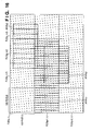
- Fig. 16 is a view for explaining the setting form of a focus detection area when detecting the lateral defocus of an object image formed by the imaging optical system.
- a first focus detection area AFAR h 1 is the most basic focus detection area in which all 30 sections included in three fields are formed into one group.
- each section which forms the second focus detection area AFAR h 2 is set over two adjacent fields.
- the number of sections is 15, which is not an integer multiple of 10 sections included in one field.
- the focus detection image sampling characteristic of each section is the same as that described with reference to Figs. 13A to 13C .
- a third focus detection area AFAR h 3 two sections are coupled into a new section.
- the average array pitch of focus detection pixels projected on the second projection line PRJ v shown in Figs. 13A to 13C is halved, but the focus detection capability is maintained.
- a section which forms a focus detection area may also be arranged over two adjacent fields.
- the size of a section and the number of sections can also be set to desired values.
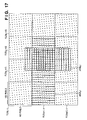
- the first focus detection area AFAR h 1 is identical to one shown in Fig. 16 , and is used to detect the lateral defocus of an object.
- the third focus detection area AFAR v 1 is used to detect the longitudinal defocus of an object.
- the characteristic of the third focus detection area AFAR v 1 is equivalent to one obtained by rotating the second focus detection area AFAR h 2 shown in Fig. 16 through 90°. That is, both the lateral and longitudinal defocuses can be simultaneously detected, and the two focus detection areas can be superposed on each other.
- the arrangement of focus detection pixels and grouping of the pixels in the first embodiment enable accurate focus detection for various objects with very high degree of freedom of setting the focus detection area.
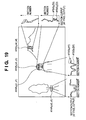
- Fig. 18 is a perspective view for conceptually explaining the imaging optical system and the pupil division state of the image sensor in the first embodiment.
- Reference symbol TL denotes an imaging optical system; 107, an image sensor; OBJ, an object; and IMG, an object image.
- an image sensing pixel receives a light beam having passed through the entire exit pupil EP of the imaging optical system.
- a focus detection pixel has the pupil division function, as described with reference to Figs. 6A, 6B , 7A, and 7B .
- the pixel S HA in Figs. 6A and 6B receives a light beam having passed through the left pupil when viewing the rear surface of the lens from the image sensing surface, that is, a light beam having passed through a pupil EP HA in Fig. 18 .
- the pixels S HB , S VC , and S VD receive light beams having passed through pupils EP HB , EP VC , and EP VD .
- focus detection pixels are distributed in the entire area of the image sensor 107, and can detect the focus in the entire image sensing area.
- the pupil shape of the focus detection pixel is a rectangle having a short side in the pupil division direction, and a long side in the direction perpendicular to it.
- the pupil shape may also be a square, polygon, semicircle, ellipse, or the like.
- the divided pupil may also protrude from the exit pupil EP of the imaging optical system.
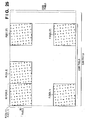
- Fig. 19 is a view for explaining an output image acquired in focus detection and a focus detection area.
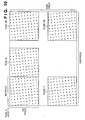
- an object image formed on the image sensing surface includes a person at the center, a tree in the foreground on the left side, and mountains in the background on the right side.
- pairs of pixels S HA and S HB for lateral defocus detection and pairs of pixels S VC and S VD for longitudinal defocus detection are arranged as focus detection pixels at equal densities in the entire image sensing area, as shown in Fig. 10 .
- AF pixel signals for calculating the phase difference are processed for each group, as shown in Fig. 12 .
- AF pixel signals for calculating the phase difference are processed for each group, as shown in Fig. 14 . Focus detection areas for lateral defocus detection and longitudinal defocus detection can be set at arbitrary positions in the image sensing area.
- a person's face exists at the center of the frame.
- a focus detection area AFAR h (x1,y1) for lateral defocus detection and a focus detection area AFAR v (x3,y3) for longitudinal defocus detection are set using the face area as a center.
- the suffix "h" represents the horizontal direction, and (x1,y1) and (x3,y3) indicate the coordinates of the upper left corners of focus detection areas. Signals from five focus detection pixels S HA included in each section of the focus detection area AFAR h (x1,y1) are added.
- a phase difference detection image A signal obtained by coupling the added signals of 30 sections is defined as AFSIG h (A1) shown in a graph on the lower side of Fig. 19 .
- signals from five focus detection pixels S HB included in each section are added, and a phase difference detection image B signal obtained by coupling the added signals of 30 sections is defined as AFSIG h (B1).
- the relative lateral defocus amounts of the image A signal AFSIG h (A1) and image B signal AFSIG h (B1) are calculated by a known correlation calculation, obtaining the defocus amount of the object.
- the defocus amount of the focus detection area AFAR v (x3,y3) is also obtained in the same way.
- the two defocus amounts detected in the focus detection areas for lateral defocus and longitudinal defocus are compared, and a value of high reliability is adopted.
- the trunk of the tree on the left side of the frame mainly has a vertical line component, that is, a luminance distribution in the lateral direction, so it is determined that the trunk is an object suitable for lateral defocus detection.
- a focus detection area AFAR h (x2,y2) for lateral defocus detection is set.
- the ridgeline of the mountains on the right side of the frame mainly has a horizontal line component, that is, a luminance distribution in the longitudinal direction, so it is determined that the ridgeline is an object suitable for longitudinal defocus detection.
- a focus detection area AFAR v (x4,y4) for longitudinal defocus detection is set.
- focus detection areas for lateral defocus detection and longitudinal defocus detection can be set at arbitrary positions in the frame. Even if the projection position of an object and the direction of the luminance distribution vary, the focus can always be detected accurately.
- Figs. 20 to 22 are flowcharts for explaining the focus adjustment and shooting processes of the camera according to the first preferred embodiment of the present invention. Control routines in Fig. 20 and subsequent drawings will be explained with reference to Figs. 1 to 19 described above.
- Fig. 20 shows the main routine of the camera according to the first embodiment.
- the CPU 121 checks the operations of the actuators and image sensor in the camera, initializes the memory contents and executing programs, and executes a shooting preparation operation in step S103.
- the CPU 121 starts the image sensing operation of the image sensor to output a low-pixel-count moving image for preview.
- the CPU 121 displays the readout moving image on the display 131 attached to the rear surface of the camera. The user visually checks the preview image and determines the shooting composition.
- step S109 the CPU 121 determines whether a face exists in the preview moving image. If the CPU 121 determines that the face exists in the shooting area, the process shifts from step S111 to step S113 to set the face AF mode as the focus adjustment mode. In the face AF mode, the camera is focused on a face in the shooting area.
- step S111 If no face exists in the shooting area, the process shifts from step S111 to step S115 to set the multi-point AF mode as the focus adjustment mode.
- step S121 the CPU 121 determines a focus detection area in step S117.
- the CPU 121 determines whether the user has turned on the shooting preparation switch. If the user has not turned on the shooting preparation switch, the process returns to step S105 to repetitively execute the processing from driving of the image sensor to determination of the focus detection area in step S117.
- step S121 determines in step S121 that the user has turned on the shooting preparation switch, the process shifts to step S131 to execute a focus detection subroutine.
- Fig. 21 is a flowchart of the focus detection subroutine.
- the CPU 121 reads out, in step S132, signals from image sensing pixels and focus detection pixels included in the focus detection area determined in step S117 of the main routine.
- the CPU 121 recognizes the direction dependency of the object contrast in the focus detection area from the readout information of image sensing pixels.
- the CPU 121 selects an image defocus detection direction suited to focus detection in accordance with the object contrast information recognized in step S133. More specifically, when the contrast of the object image exists in only the horizontal direction, focus detection is done using only lateral defocus detection pixels. Similarly, when the contrast of the object image exists in only the vertical direction, focus detection is done using only longitudinal defocus detection pixels. When the contrast exists in both the horizontal and vertical directions, cross focus detection is done using both lateral and longitudinal defocus detection pixels.
- step S141 the CPU 121 adds signals from focus detection pixels in each section on the basis of the section structure shown in Fig. 12 or 14 in the focus detection area selected in step S134, obtaining an AF pixel signal.
- step S142 the AF pixel signal obtained in step S141 undergoes shading correction (light fall-off correction at the periphery of the frame), correction of distortion of two images caused by vignetting, and the like, thereby obtaining two image signals for correlation calculation.
- shading correction light fall-off correction at the periphery of the frame
- correction of distortion of two images caused by vignetting and the like
- step S143 the CPU 121 calculates the correlation between the two obtained images, calculating the relative positional error amount between the two images.
- step S144 the CPU 121 determines the reliability of the calculated correlation.
- the reliability means the coincidence between two images, and when the coincidence between two images is high, the reliability of the focus detection result is generally high. When a plurality of focus detection areas are selected, information having high reliability is preferentially used. Even when cross focus detection is selected to detect image shifts in two directions, the reliability of the correlation in each direction is evaluated, and if the reliability is lower than a threshold, the detection result is not adopted.
- step S145 the CPU 121 calculates a defocus amount from the detection result having high reliability.
- step S146 the process returns to step S131 in the main routine of Fig. 20 .
- step S151 of Fig. 20 the CPU 121 determines whether the defocus amount calculated in step S143 of Fig. 21 is less than or equal to an allowance. If the defocus amount exceeds the allowance, the CPU 121 determines that the image is out of focus, drives the focus lens in step S153, and then repetitively executes steps S131 to S151. If the CPU 121 determines in step S151 that the image is in focus, the CPU 121 presents an in-focus display in step S155, and shifts to step S157.
- step S157 the CPU 121 determines whether the user has turned on the shooting start switch. If the user has not turned on the shooting start switch, the CPU 121 maintains the shooting standby state in step S157. If the CPU 121 determines in step S157 that the user has turned on the shooting start switch, the process shifts to step S161 to execute a shooting subroutine.
- Fig. 22 is a flowchart of the shooting subroutine.
- the CPU 121 drives the light quantity adjustment stop in step S163 after step S161, controlling the aperture of the mechanical shutter for defining the exposure time.
- the CPU 121 reads out an image for sensing a still image using a large number of pixels, that is, reads out signals from all pixels.
- the CPU 121 interpolates an omitted pixel in the readout image signal. That is, an output from a focus detection pixel does not contain RGB color information for image sensing, and the focus detection pixel appears as a defective pixel when obtaining an image. Hence, an image signal is generated by interpolation using information from peripheral image sensing pixels.
- the CPU 121 performs image processes such as ⁇ correction and edge emphasis for the image in step S169, and records a sensed image in the flash memory 133 in step S171.
- the CPU 121 displays the sensed image on the display 131 in step S173.
- the process returns to the main routine of Fig. 20 .
- step S181 After returning to the main routine of Fig. 20 , the CPU 121 ends a series of shooting operations in step S181.
- the above-described first embodiment has the following effects.
- Lateral defocus detection pixels and longitudinal defocus detection pixels are arranged at almost equal intervals and equal densities near the lattice points of a 2-dimensional lattice. This arrangement enables accurate focus detection for both an object having a luminance distribution in the lateral direction and an object having a luminance distribution in the longitudinal direction.
- the unit area is divided into a plurality of individual areas, and a plurality of pixel signals in each individual area are synthesized to generate a focus detection calculation signal.
- the number of calculation pixels can be decreased to shorten the time taken for focus detection calculation without impairing the focus detection capability.
- a plurality of unit areas are arranged in the image sensing area of the image sensing unit. This can simplify the pixel array rule, and also simplify the algorithms of focus detection calculation and output image generation calculation.
- paired lateral defocus detection pixels or paired longitudinal defocus detection pixels are assigned to the positions of R and B pixels diagonally adjacent to each other.
- focus detection pixels are assigned to the positions of pixels of a single color, that is, only R or B pixels. The arrangement of the second embodiment will be explained with reference to Figs. 23 to 26 .
- Fig. 23 is a view showing a focus detection pixel array according to the second embodiment, and corresponds to Fig. 8 in the first embodiment.
- focus detection pixels S HA , S HB , Svc and S VD are assigned to the positions of R and B pixels diagonally adjacent to each other among image sensing pixels having the Bayer array.
- focus detection pixels are assigned to only B pixels in the Bayer array. More specifically, in each of the top left block BLK(1,1) and lower right block BLK(2,2), two B pixels near the left on the bottom row are replaced with a pair of focus detection pixels S HA and S HB for dividing the pupil in the horizontal direction.
- a focus detection pixel for horizontal pupil division is arranged in a block BLK(i,j) when i+j is an even number, and a focus detection pixel for vertical pupil division is arranged in it when i+j is an odd number, similar to the first embodiment.
- Fig. 24 is a view for explaining an arrangement rule for the cluster serving as a unit, and corresponds to Fig. 9 in the first embodiment.
- B pixels near the lower left corner of each block are replaced with focus detection pixels S HA and S HA or S VC and S VD .
- a cluster CST(1,2) on the right side of the cluster CTS(1,1) focus detection pixels in each block are arranged at positions shifted up by two pixels from those in the cluster CST(1,1).
- a cluster CST(2,1) below the first cluster CTS(1, 1) focus detection pixels in each block are arranged at positions shifted to the right by two pixels from those in the cluster CST(1,1).
- This rule is repetitively applied to obtain the arrangement shown in Fig. 24 .
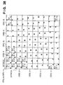
- Fig. 25 is a view for explaining an arrangement rule for the field serving as a unit, and corresponds to Fig. 10 in the first embodiment.
- all fields FLD(q,r) have the same array as that of the first field FLD(1, 1).
- An incomplete area of 40 columns at the right end cannot form one field, and no focus detection pixel is arranged in this area.
- focus detection pixels can be distributed almost uniformly in the entire image sensing area.
- the definitions of ⁇ and ⁇ are the same as those in Fig. 11 .
- ⁇ represents a point where the first focus detection pixel group for dividing the exit pupil of the imaging optical system in the lateral direction (right-to-left direction or horizontal direction) is arranged.
- ⁇ represents a point where the second focus detection pixel group for dividing the pupil in the longitudinal direction (up-to-bottom direction or vertical direction) is arranged.
- LTH1 to LTH8 form a first lattice line group of lattice lines each formed by linking ⁇ in the lateral direction.
- a direction in which the first lattice line group extends is inclined counterclockwise by ⁇ LH from a horizontal line.
- a lattice pitch P LH which is the arrangement interval between adjacent lattice lines of the first lattice line group, is 10 (pixels), similar to the first embodiment.
- LTV1 to LTV8 form a second lattice line group of lattice lines each formed by linking ⁇ in the vertical direction.
- a lattice pitch P LV which is the arrangement interval between adjacent lattice lines of the second lattice line group, is also 10 (pixels).
- the first lattice line group is formed from parallel lines which extend in a direction almost coincident with the first pupil division direction and are arranged equally at predetermined pitches.
- the second lattice line group is formed from parallel lines which extend in a direction almost coincident with the second pupil division direction and are arranged equally at predetermined pitches.
- the two lattice line groups cross each other perpendicularly to form a 2-dimensional lattice. Focus detection pixels are periodically arranged near the lattice points.
- the first focus detection pixel is arranged on one lattice line, and the second focus detection pixel is arranged on the other lattice line. This can decrease the arrangement density of focus detection pixels while maintaining pupil division direction functions in two directions.
- each lattice line is disconnected, that is, slightly shifted from each other at the boundary between fields.
- the focus detection image sampling characteristic is the same as that described with reference to Figs. 12 to 15A , 15B, and 15C in the first embodiment, and a detailed description thereof will not be repeated.
- As a focus detection area setting method the same methods as those in Figs. 16 and 17 in the first embodiment can be adopted.
- As a focus detection routine those in Figs. 18 to 22 can be used. As a result, almost the same focus detection characteristic as that in the first embodiment can be obtained.
- the second embodiment can similarly obtain effects (1-1) to (1-4) in the first embodiment, and also attains, for example, the following effect.
- Focus detection pixels are assigned to pixels of a single color, simplifying the defective pixel interpolation algorithm when generating an output image. The degradation and false color of an image in a specific color can be reduced.
- two focus detection pixels are paired, one pixel receives a light beam having passed through one pupil of two divided pupil areas, and the other pixel receives a light beam having passed through the other pupil.
- the third embodiment will describe an image sensor in which one pixel receives light beams from two divided pupil areas to output the signals.
- Fig. 27 is a view showing a focus detection pixel array according to the third embodiment, and corresponds to Fig. 8 in the first embodiment.
- focus detection pixels S HA , S HB , S VC and S VD are assigned to the positions of R and B pixels diagonally adjacent to each other among image sensing pixels having the Bayer array.
- the focus detection pixel S HAB can be formed by a technique disclosed in Japanese Patent Laid-Open No. 2003-156677 filed by the present applicant. More specifically, like an image sensor disclosed in Japanese Patent Laid-Open No. 2003-156677 , a photoelectric conversion portion behind an on-chip microlens is divided to divide the pupil of an imaging optical system. A light beam having passed through each divided pupil area is independently received and output as an image signal. Hence, one pixel can output a pair of signals for phase difference detection.
- one R pixel near the bottom on the leftmost column is replaced with one focus detection pixel S VCD for dividing the pupil in the vertical direction.
- a focus detection pixel for horizontal pupil division is arranged in a block BLK(i, j) when i+j is an even number, and a focus detection pixel for vertical pupil division is arranged in it when i+j is an odd number, similar to the first embodiment.
- Fig. 28 is a view for explaining a rule to arrange a set of clusters each serving as a unit, and corresponds to Fig. 9 in the first embodiment.
- the entire area shown in Fig. 28 represents one field superordinate to the cluster.
- the arrangement rule of the field is the same as that in the first embodiment.
- a lattice representing the arrangement of focus detection pixels is identical to a 2-dimensional lattice shown in Fig. 11 in the first embodiment.
- the field arrangement in the entire image sensing area, the focus detection characteristic, and the focus detection routine are the same as those shown in Figs. 10 to 22 in the first embodiment, and a description thereof will not be repeated.
- the third embodiment can similarly obtain effects (1-1) to (1-4) in the first embodiment, and also attains, for example, the following effect.
- the number of pixels assigned as focus detection pixels can be decreased, further reducing the degradation and false color of an output image.
- even the defective pixel interpolation algorithm when generating an output image can be simplified.
- a 2-dimensional lattice representing the array of focus detection pixels is an orthogonal lattice. Each lattice line is rotated in one direction by only a predetermined angle from a horizontal or vertical line serving as an image sensing pixel array line.
- at least part of a 2-dimensional lattice is a non-orthogonal lattice, and lattice line rotational directions are two, positive and negative directions with respect to a horizontal or vertical line. The arrangement of the fourth embodiment will be explained with reference to Figs. 29 to 31 .
- Fig. 29 is a view showing a focus detection pixel array according to the fourth embodiment, and corresponds to Fig. 9 in the first embodiment.
- a block serving as the minimum unit of the pixel array, and a cluster superordinate to the block are determined by the same rules as those in Fig. 8 in the first embodiment.
- the field size is the same as that in the first embodiment, but fields of four types complying with different arrangement rules are arranged.
- Fig. 29 shows two types of fields out of four types of fields in the fourth embodiment.
- 5 ⁇ 5 25 clusters on the left side form the first field having the same pixel array as that in the first embodiment. More specifically, in a cluster CST(u,w) in the field, the focus detection pixel shifts to the right as u increases, and shifts up as w increases. This rule is applied to clusters CST(1, 1) to CST(5,5).
- the second field is arranged on the right side of the first field.
- the focus detection pixel shifts to the right as u increases, similar to the above-described rule, but shifts down as w increases.
- the third field (not shown) is arranged below the first field.
- the focus detection pixel shifts to the left as u increases, and shifts up as w increases.
- the fourth field is arranged on the right side of the third field.
- the focus detection pixel shifts to the left as u increases, and shifts down as w increases.
- Fig. 30 shows a set of fields formed according to the above-described rules.
- 2 ⁇ 2 4 fields serve as a most superordinate unit in the pixel arrangement rules
- Fig. 30 shows four most superordinate units.
- the horizontal argument of a lattice line extending in the lateral direction is +5.7°
- the vertical argument of a lattice line extending in the longitudinal direction is also +5.7°.
- the crossing angle of the two lattice lines is a right angle, and such lattice lines form an orthogonal lattice.
- the horizontal argument of a lattice line extending in the lateral direction is -5.7°
- the vertical argument of a lattice line extending in the longitudinal direction is +5.7°.
- the crossing angle of the two lattice lines is about 80°, and such lattice lines form a non-orthogonal lattice.
- the horizontal argument of a lattice line extending in the lateral direction is +5.7°
- the vertical argument of a lattice line extending in the longitudinal direction is -5.7°.
- the crossing angle of the two lattice lines is about 80°, and such lattice lines form a non-orthogonal lattice.
- the horizontal argument of a lattice line extending in the lateral direction is -5.7°
- the vertical argument of a lattice line extending in the longitudinal direction is also -5.7°.
- the crossing angle of the two lattice lines is a right angle, and such lattice lines form an orthogonal lattice.
- the horizontal and vertical arguments of lattice lines take positive and negative signs, and the arguments of lattice lines are averaged to be substantially 0 in the entire image sensing area.
- the sampling characteristic of focus detection pixels and the defective pixel distribution when generating an output image are different between a lateral line inclined by + ⁇ ( ⁇ ⁇ a small angle of about 5°) from a horizontal line and a lateral line inclined by - ⁇ .
- the characteristics in one field are the same as those in the first to third embodiments.
- positive and negative arguments cancel each other in a wide range of several fields, reducing the influence of the differences.
- the section arrangement, focus detection area setting method, focus detection characteristic, and focus detection routine in focus detection are the same as those shown in Figs. 12 to 22 in the first embodiment, and a description thereof will not be repeated.
- the fourth embodiment can similarly obtain effects (1-1) to (1-4) in the first embodiment, and also attains, for example, the following effects.
- a focus detection pixel appears as a defective pixel in an output image.
- positive and negative, horizontal and vertical arguments of lattice lines coupling defective pixels coexist, so degradation of the image quality and generation of an unnatural image can be reduced even for a geometrical pattern including many straight lines.
- the position of a focus detection pixel in a block is shifted sequentially between clusters.
- the fifth embodiment does not employ this shift rule, and focus detection pixels are arrayed in a complete square lattice. The arrangement of the fifth embodiment will be explained with reference to Figs. 32 to 34 .
- Fig. 32 is a view showing a focus detection pixel array according to the fifth embodiment, and corresponds to Fig. 9 in the first embodiment.
- a block serving as the minimum unit of the pixel array is determined by the same rule as that in Fig. 8 in the first embodiment.
- the position of a focus detection pixel is shifted sequentially between clusters in the first to fourth embodiments.
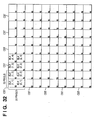
- Fig. 33 shows a pixel array in the entire image sensing area.
- an area of 100 ⁇ 100 10,000 pixels is defined as a field for descriptive convenience.
- the field size is arbitrary.
- the horizontal argument of a lattice line extending in the lateral direction is 0°
- the vertical argument of a lattice line extending in the longitudinal direction is also 0°.
- the crossing angle of the two lattice lines is a right angle, and such lattice lines form an orthogonal lattice.
- the focus detection capability for a thin line extending in the horizontal or vertical direction is not the same as that in the first to fourth embodiments.
- the sampling characteristic of a focus detection image in the pupil division direction is improved by shifting a focus detection pixel between clusters.
- no focus detection pixel is shifted between clusters, and the capturing characteristic of a thin line image extending in the horizontal or vertical direction,slightly decreases.
- this drawback can be compensated by decreasing the pitch between image sensing pixels and increasing the number of pixels of the image sensor.
- the section arrangement, focus detection area setting method, and focus detection routine in focus detection are the same as those shown in Figs. 16 to 22 in the first embodiment, and a description thereof will not be repeated.
- the fifth embodiment can similarly obtain effects (1-1) and (1-2) in the first embodiment, and also attains, for example, the following effect.
- lateral defocus detection pixels and longitudinal defocus detection pixels are arranged at equal densities.
- lateral defocus detection pixels and longitudinal defocus detection pixels are arranged at different densities. The arrangement of the sixth embodiment will be explained with reference to Figs. 35 to 38 .
- Fig. 35 is a view showing a focus detection pixel array according to the sixth embodiment, and corresponds to Fig. 8 in the first embodiment.
- focus detection pixels S HA and S HB for dividing the pupil in the horizontal direction are arranged in the upper left block BLK(1, 1) and lower right block BLK(2,2).
- Focus detection pixels S VC and S VD for dividing the pupil in the vertical direction are arranged in the remaining blocks BLK(1,2) and BLK(2,1).
- focus detection pixels S HA and S HB for dividing the pupil in the horizontal direction are arranged in three blocks BLK(1, 1), BLK(2, 1), and BLK(2, 2).
- Focus detection pixels S VC and S VD for dividing the pupil in the vertical direction are arranged in one remaining block BLK(1,2).
- Fig. 36 is a view for explaining an arrangement rule using the cluster as a unit, and corresponds to Fig. 9 in the first embodiment.
- the arrangement rule of pixels in a cluster according to the sixth embodiment is different from that in the first embodiment, but the arrangement rules of units superordinate to the cluster are the same as those in the first embodiment.
- the arrangement rule of fields in Fig. 36 is the same as that in Fig. 9 in the first embodiment.
- Fig. 37 is a view for explaining an arrangement rule using the field as a unit, and corresponds to Fig. 10 in the first embodiment.
- the arrangement rule of fields in the sixth embodiment is the same as that in the first embodiment, so the arrangement in Fig. 37 is the same as that Fig. 10 .
- the ratio of the number of lattice points ⁇ for lateral defocus detection and that of lattice points ⁇ for longitudinal defocus detection is 3 : 1.
- Both the horizontal argument of a lattice line extending in the lateral direction and the vertical argument of a lattice line extending in the longitudinal direction are +5.7°, similar to the first embodiment.
- the crossing angle of the two lattice lines is a right angle, and such lattice lines form an orthogonal lattice.
- the shape of the 2-dimensional lattice is the same as that in the first embodiment, but the arrangement order and arrangement ratio of focus detection pixels arranged at lattice points are different.
- focus detection capability for an object having a luminance distribution in the horizontal direction increases, and focus detection capability for an object having a luminance distribution in the vertical direction decreases.
- the sixth embodiment is suitable for a case wherein the luminance distribution of an object to be sensed is anisotropic, for example, for an inspection camera which inspects a printed-wiring board mainly having horizontal lines.
- the application of the sixth embodiment is not limited to this.
- the section arrangement, focus detection area setting method, and focus detection routine in focus detection are the same as those shown in Figs. 16 to 22 in the first embodiment, and a description thereof will not be repeated.
- the sixth embodiment can similarly obtain effects (1-1) to (1-4) in the first embodiment, and also attains, for example, the following effect.
- either a lateral defocus detection pixel or longitudinal defocus detection pixel is always arranged in a unit block.
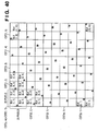
- blocks in which focus detection pixels are arranged, and blocks in which no focus detection pixel is arranged coexist. The arrangement of the seventh embodiment will be explained with reference to Figs. 39 to 42 .
- Fig. 39 is a view showing a focus detection pixel array according to the seventh embodiment, and corresponds to Fig. 8 in the first embodiment.
- focus detection pixels S HA and S HB for dividing the pupil in the horizontal direction are arranged in the upper left block BLK(1, 1) and lower right block BLK(2,2).
- Focus detection pixels S VC and S VD for dividing the pupil in the vertical direction are arranged in the remaining blocks BLK(1,2) and BLK(2,1).
- focus detection pixels S HA and S HB for dividing the pupil in the horizontal direction are arranged in the upper left block BLK(1, 1).
- Focus detection pixels S VC and S VD for dividing the pupil in the vertical direction are arranged in the lower right block BLK(2,2). No focus detection pixel is arranged in the two remaining blocks BLK(1,2) and BLK(2,1).
- the ratio of blocks in which lateral defocus detection pixels are arranged, blocks in which longitudinal defocus detection pixels are arranged, and blocks in which no focus detection pixel is arranged is 1 : 1 : 2.
- Fig. 40 is a view for explaining an arrangement rule using the cluster as a unit, and corresponds to Fig. 9 in the first embodiment.
- the arrangement rule of pixels in a cluster according to the seventh embodiment is different from that in the first embodiment, but the arrangement rules of units superordinate to the cluster are the same as those in the first embodiment.
- the arrangement rule of fields in Fig. 40 is the same as that in Fig. 9 in the first embodiment.
- ⁇ and ⁇ are arranged at the lattice points of individual lattice lines of a 2-dimensional lattice. More specifically, in one field, only ⁇ are arranged on the lattice lines of a 2-dimensional lattice that pass through lattice points ⁇ for lateral defocus detection, and no ⁇ is arranged. Similarly, only ⁇ are arranged on the lattice lines of a 2-dimensional lattice that pass through lattice points ⁇ for longitudinal defocus detection, and no ⁇ is arranged.
- Both the horizontal argument of a lattice line extending in the lateral direction and the vertical argument of a lattice line extending in the longitudinal direction are +5.7°, similar to the first embodiment.
- the crossing angle of the two lattice lines is a right angle, and such lattice lines form an orthogonal lattice.
- each lattice line is discontinuous at the boundary between fields. More specifically, when a lattice line of ⁇ in one field extends to an adjacent field, it is connected to a lattice line of ⁇ . Similarly, when a lattice line of ⁇ extends to an adjacent field, it is connected to a lattice line of ⁇ .
- Fig. 43 shows a modification which solves this discontinuity. In the modification of Fig. 43 , four fields are equal in the pitch and argument of lattice lines, but different in the arrangement rule of ⁇ and ⁇ . More specifically, the arrangement rule of lateral defocus detection pixels and longitudinal defocus detection pixels is changed between four fields. Four fields are defined as a new unit to form an image sensing area, thereby solving the discontinuity between fields.
- the shape of the 2-dimensional lattice in the seventh embodiment is the same as that in the first embodiment, but the arrangement density of focus detection pixels arranged at lattice points is halved.
- the section arrangement, focus detection area setting method, and focus detection routine in focus detection are the same as those shown in Figs. 16 to 22 in the first embodiment, and a description thereof will not be repeated.
- the seventh embodiment can similarly obtain effects (1-1) to (1-4) in the first embodiment, and also attains, for example, the following effect.
- the arrangement density of focus detection pixels can be decreased. Even in an image sensor having many pixels, an excessively large load of focus detection calculation and a long focusing time can be prevented.
- the first to seventh embodiments have exemplified a digital still camera.
- the focus detection apparatus based on the technique of the present invention is applicable not only to the digital still camera, but also to a camcorder (movie camera) for recording a moving image, various inspection cameras, a monitoring camera, an endoscope camera, a robot camera, and the like.
- square pixels each having an aspect ratio of 1 : 1 are arranged in a square on a 2-dimensional surface.
- the present invention is also applicable to an image sensor having not the square arrangement, but, for example, a honeycomb arrangement.
- the color filter of the image sensor is not limited to the RGB color filter.
Description
- The present invention relates to an image sensor capable of sensing at least either still images or moving images using many two-dimensionally arrayed photoelectric conversion elements, and a method of detecting a focus state in an image sensing apparatus using the image sensor.
- A contrast detection method (called a blur detection method) and a phase difference detection method (called a defocus detection method) have been proposed as general methods using a light beam having passed through an imaging optical system in automatic focus detection/adjustment of an image sensing apparatus.
- The contrast detection method is often used in a video movie camera (camcorder) for recording a moving image, and an electronic still camera. The image sensor is used as a focus detection sensor. This method pays attention to the output signal of the image sensor, especially high-frequency component information (contrast information), and a position of the imaging optical system where the evaluation value maximizes is set as an in-focus position. However, this contrast detection method, also called a hill-climbing detection method, is not suitable for a high-speed focus adjustment operation because the evaluation value is obtained while slightly moving the imaging optical system, and the imaging optical system needs to be moved until it is determined that the evaluation value was maximum.
- The phase difference detection method is generally adopted in single-lens reflex cameras using a silver halide film, and is a technique most contributed to practical use of AF (Auto Focus) single-lens reflex cameras. According to the phase difference detection method, a light beam having passed through the exit pupil of the imaging optical system is split into two, and the two light beams are received by a pair of focus detection sensors. The defocus amount of the imaging optical system in the focusing direction is directly obtained by detecting the difference between signals output in accordance with the light reception amounts, that is, the relative positional error amount in the direction in which the light beam is split. Once the focus detection sensor executes the accumulation operation, the defocus amount and direction can be attained to perform a high-speed focus adjustment operation. To split a light beam having passed through the exit pupil of the imaging optical system into two, and obtain signals corresponding to the two light beams, an optical path division means such as a quick return mirror or half-mirror is generally inserted in the image sensing optical path, and a focus detection optical system and AF sensor are arranged on the output side of the optical path division means. This structure makes the device bulky and expensive.
- To solve this problem, there is also disclosed a technique of adding a phase difference detection function to an image sensor to eliminate a dedicated AF sensor and implement high-speed phase difference AF.
- For example, in Japanese Patent Laid-Open No.
2000-156823 - In Japanese Patent Laid-Open No.
2000-292686 - In Japanese Patent Laid-Open No.
2001-305415 - In Japanese Patent Laid-Open No.
2003-153291 - Items which should be considered when executing phase difference detection AF using an image sensor will be listed below. As for the AF performance, the following items need to be satisfied.
- (a) Focus can be detected regardless of the direction of the luminance distribution of an object. In other words, the focus can be detected along vertical, horizontal, and oblique lines.
- (b) Focus detection image sampling error is very small, and the focus detection precision is independent of the spatial frequency and phase of an object.
- (c) Focus can be detected in an arbitrary area.
- (d) The S/N ratio of a focus detection image signal is high even for a low-brightness object, and the focus detection precision does not decrease.
- (e) The arrangement coordinates of focus detection pixels are regular, and the algorithms of focus detection pixel signal processing and focus detection calculation are simple.
- When generating an output image, focus detection pixels function as singular or defective pixels. To prevent degradation of an output image, the following items need to be satisfied.
- (i) The ratio of the number of focus detection pixels to the total number of pixels of an image sensor is low.
- (ii) Focus detection pixels are distributed uniformly.
- (iii) The arrangement coordinates of focus detection pixels are regular, and the defective pixel interpolation algorithm is simple.
- An increase in focus detection precision and prevention of degradation of an output image generally have a trade-off relationship. An advanced technique is required to satisfy all the listed items while balancing them. However, the above-mentioned conventional techniques suffer the following disadvantages.
- The technique disclosed in Japanese Patent Laid-Open No.
2000-156823 - The technique disclosed in Japanese Patent Laid-Open No.
2000-292686 - The technique disclosed in Japanese Patent Laid-Open No.
2001-305415 - The technique disclosed in Japanese Patent Laid-Open No.
2003-153291 -
US 2007/206940 discloses a focus adjustment device includes focus detection pixels for detecting a focus adjustment state of an imaging optical system through a first pupil division-type image shift detection method, a focus detector that detects a focus adjustment state at the imaging optical system through a second pupil division-type image shift detection method different from the first pupil division-type image shift detection method. - The present invention has been made to overcome the conventional drawbacks, and has as its object to enable detection of phase differences in two directions at an arbitrary position in a predetermined unit area of an image sensing unit, and detecting the focus of even an object having contrast information in only one direction.
- According to the first aspect of the present invention, there is provided an image sensor as claimed in
claim 1 herein. - According to the second aspect of the present invention, there is provided a focus detection as claimed in
claim 6 herein. - Further features of the present invention will become apparent from the following description of exemplary embodiments with reference to the attached drawings.
-
-
Fig. 1 is a view of the arrangement of a camera according to a preferred embodiment of the present invention; -
Fig. 2 is a circuit diagram of an image sensor according to the preferred embodiment of the present invention; -
Fig. 3 is a sectional view of the pixel portion of the image sensor according to the preferred embodiment of the present invention; -
Fig. 4 is a driving timing chart of the image sensor according to the preferred embodiment of the present invention; -
Figs. 5A and 5B are a plan view and sectional view, respectively, showing the image sensing pixel of the image sensor according to the first preferred embodiment of the present invention; -
Figs. 6A and 6B are a plan view and sectional view, respectively, showing a focus detection pixel of the image sensor according to the first preferred embodiment of the present invention; -
Figs. 7A and 7B are a plan view and sectional view, respectively, showing another focus detection pixel of the image sensor according to the first preferred embodiment of the present invention; -
Fig. 8 is a view for explaining a pixel array serving as a minimum unit in the image sensor according to the first preferred embodiment of the present invention; -
Fig. 9 is a view for explaining a pixel array serving as a superordinate unit in the image sensor according to the first preferred embodiment of the present invention; -
Fig. 10 is a view for explaining a pixel array in the entire area of the image sensor according to the first preferred embodiment of the present invention; -
Fig. 11 is a view for explaining the array of focus detection pixels as a 2-dimensional lattice according to the first preferred embodiment of the present invention; -
Fig. 12 is a view for explaining a pixel grouping method in lateral defocus detection according to the first preferred embodiment of the present invention; -
Figs. 13A to 13C are views for explaining an image sampling characteristic in lateral defocus detection according to the first preferred embodiment of the present invention; -
Fig. 14 is a view for explaining a pixel grouping method in longitudinal defocus detection according to the first preferred embodiment of the present invention; -
Figs. 15A to 15C are views for explaining an image sampling characteristic in longitudinal defocus detection according to the first preferred embodiment of the present invention; -
Fig. 16 is a view for explaining a focus detection area setting method in lateral defocus detection according to the first preferred embodiment of the present invention; -
Fig. 17 is a view for explaining a focus detection area setting method in cross focus detection according to the first preferred embodiment of the present invention; -
Fig. 18 is a conceptual view for explaining the pupil division state of the image sensor according to the first preferred embodiment of the present invention; -
Fig. 19 is a view for explaining a focus detection area according to the first preferred embodiment of the present invention; -
Fig. 20 is a flowchart of a main control routine according to the first preferred embodiment of the present invention; -
Fig. 21 is a flowchart of a focus detection subroutine according to the first preferred embodiment of the present invention; -
Fig. 22 is a flowchart of a shooting subroutine according to the first preferred embodiment of the present invention; -
Fig. 23 is a view for explaining a pixel array serving as a minimum unit in an image sensor according to the second preferred embodiment of the present invention; -
Fig. 24 is a view for explaining a pixel array serving as a superordinate unit in the image sensor according to the second preferred embodiment of the present invention; -
Fig. 25 is a view for explaining a pixel array in the entire area of the image sensor according to the second preferred embodiment of the present invention; -
Fig. 26 is a view for explaining the array of focus detection pixels as a 2-dimensional lattice according to the second preferred embodiment of the present invention; -
Fig. 27 is a view for explaining a pixel array serving as a minimum unit in an image sensor according to the third preferred embodiment of the present invention; -
Fig. 28 is a view for explaining a pixel array serving as a superordinate unit in the image sensor according to the third preferred embodiment of the present invention; -
Fig. 29 is a view for explaining a pixel array serving as a superordinate unit in an image sensor according to the fourth preferred embodiment of the present invention; -
Fig. 30 is a view for explaining a pixel array in the entire area of the image sensor according to the fourth preferred embodiment of the present invention; -
Fig. 31 is a view for explaining the array of focus detection pixels as a 2-dimensional lattice according to the fourth preferred embodiment of the present invention; -
Fig. 32 is a view for explaining a pixel array serving as a superordinate unit in an image sensor according to the fifth preferred embodiment of the present invention; -
Fig. 33 is a view for explaining a pixel array in the entire area of the image sensor according to the fifth preferred embodiment of the present invention; -
Fig. 34 is a view for explaining the array of focus detection pixels as a 2-dimensional lattice according to the fifth preferred embodiment of the present invention; -
Fig. 35 is a view for explaining a pixel array serving as a minimum unit in an image sensor according to the sixth preferred embodiment of the present invention; -
Fig. 36 is a view for explaining a pixel array serving as a superordinate unit in the image sensor according to the sixth preferred embodiment of the present invention; -
Fig. 37 is a view for explaining a pixel array in the entire area of the image sensor according to the sixth preferred embodiment of the present invention; -
Fig. 38 is a view for explaining the array of focus detection pixels as a 2-dimensional lattice according to the sixth preferred embodiment of the present invention; -
Fig. 39 is a view for explaining a pixel array serving as a minimum unit in an image sensor according to the seventh preferred embodiment of the present invention; -
Fig. 40 is a view for explaining a pixel array serving as a superordinate unit in the image sensor according to the seventh preferred embodiment of the present invention; -
Fig. 41 is a view for explaining a pixel array in the entire area of the image sensor according to the seventh preferred embodiment of the present invention; -
Fig. 42 is a view for explaining an array of focus detection pixels as a 2-dimensional lattice according to the seventh preferred embodiment of the present invention; and -
Fig. 43 is a view for explaining another array of focus detection pixels as a 2-dimensional lattice according to the seventh preferred embodiment of the present invention. - Preferred embodiments of the present invention will be described below.
-
Figs. 1 to 22 are views according to the first preferred embodiment of the present invention. The first embodiment will be explained with reference to these drawings. -
Fig. 1 is a view of the arrangement of a camera according to the preferred embodiment of the present invention.Fig. 1 shows an electronic camera configured by integrating a camera body having an image sensor serving as an image sensing unit, and an imaging optical system. InFig. 1 , afirst lens group 101 is arranged on the first stage of the imaging optical system (image forming optical system), and is held reciprocally along the optical axis. A stop/shutter 102 adjusts the aperture diameter to adjust the light quantity in shooting. The stop/shutter 102 also functions as a shutter for adjusting the exposure time when sensing a still image. The stop/shutter 102 and asecond lens group 103 reciprocate together along the optical axis to achieve a zooming operation (zooming function) in synchronism with the reciprocal operation of thefirst lens group 101. - A
third lens group 105 reciprocates along the optical axis to adjust the focus. Anoptical lowpass filter 106 is an optical element for reducing the false color and moire of a sensed image. Animage sensor 107 includes a C-MOS sensor and its peripheral circuit. The image sensor is a two-dimensional 1CCD color sensor in which a primary color mosaic filter with the Bayer array is formed on a chip of m light receiving pixels in the horizontal direction and n light receiving pixels in the vertical direction. - By pivoting a cam cylinder (not shown), a
zoom actuator 111 drives thefirst lens group 101 tothird lens group 105 to reciprocate along the optical axis and perform the zooming operation. A stop/shutter actuator shutter 102 to adjust the light quantity in shooting, and controls the exposure time when sensing a still image. Afocus actuator 114 drives thethird lens group 105 to reciprocate along the optical axis and adjust the focus. - An
electronic flash 115 is used to illuminate an object in shooting. Theelectronic flash 115 is preferably a flash illumination device using a xenon tube, but may also be an illumination device having a continuous emission LED. An AF auxiliarylight unit 116 projects, to the field via a projection lens, an image of a mask having a predetermined aperture pattern, and improves the focus detection capability for a dark object or low-contrast object. - A
CPU 121 in the camera executes various control operations of the camera body. TheCPU 121 includes, for example, an arithmetic unit, ROM, RAM, A/D converter, D/A converter, communication interface circuit, and the like. Based on a predetermined program stored in the ROM, theCPU 121 drives various circuits of the camera to execute a series of operations such as AF, shooting, image processing, and recording. - An electronic
flash control circuit 122 controls the ON operation of theelectronic flash 115 in synchronism with the shooting operation. An auxiliarylight driving circuit 123 controls the ON operation of the AF auxiliarylight unit 116 in synchronism with a focus detection operation of detecting the focus state of the image forming optical system. An imagesensor driving circuit 124 controls the image sensing operation of theimage sensor 107, A/D-converts an acquired image signal, and transmits the digital data to theCPU 121. Animage processing circuit 125 performs processes such as γ conversion, color interpolation, and JPEG compression for an image obtained by theimage sensor 107. - A
focus driving circuit 126 controls to drive thefocus actuator 114 on the basis of the focus detection result, and drives thethird lens group 105 to reciprocate along the optical axis, thereby adjusting the focus. A stop/shutter driving circuit 128 controls to drive the stop/shutter actuator 112, thereby controlling the aperture of the stop/shutter 102. Azoom driving circuit 129 drives thezoom actuator 111 in accordance with the zooming operation of the user. - A
display 131 is, for example, an LCD, and displays information on the shooting mode of the camera, a preview image before shooting, a confirmation image after shooting, an in-focus display image upon focus detection, and the like. Operation switches 132 include a power switch, release (shooting trigger) switch, zooming operation switch, shooting mode selection switch, and the like. Adetachable flash memory 133 records a sensed image. -
Fig. 2 is a schematic circuit diagram of the image sensor according to the preferred embodiment of the present invention. The image sensor is manufactured according to a technique disclosed in, for example, Japanese Patent Laid-Open No.09-046596 Fig. 2 shows a pixel area of two columns × four rows in a two-dimensional C-MOS area sensor. When the area sensor is used as an image sensor, many pixels each shown inFig. 2 are arranged to be able to obtain a high-resolution image. The embodiment will describe a digital still camera image sensor having a pixel pitch of 2 µm, effective pixels on 3,000 columns × 2,000 rows = 6,000,000 pixels, and an image sensing frame size of 6 mm in width × 4 mm in length. - In
Fig. 2 , aphotoelectric conversion portion 1 of a photoelectric conversion element is formed from a MOS transistor gate and a depletion layer below the gate.Reference numeral 2 denotes a photogate; and 3, a transfer switch MOS transistor.Reference numeral 4 denotes a reset MOS transistor; 5, a source follower amplifier MOS transistor; 6, a horizontal selection switch MOS transistor; and 7, a source follower load MOS transistor.Reference numeral 8 denotes a dark output transfer MOS transistor; 9, a bright output transfer MOS transistor; 10, a dark output accumulation capacitor CTN; 11, a bright output accumulation capacitor CTS; and 12, a horizontal transfer MOS transistor.Reference numeral 13 denotes a horizontal output line reset MOS transistor; 14, a differential output amplifier; 15, a horizontal scanning circuit; and 16, a vertical scanning circuit. -
Fig. 3 is a sectional view of a pixel portion. InFig. 3 ,reference numeral 17 denotes a P-well; 18, a gate oxide film; 19, a first poly-Si layer; 20, a second poly-Si layer; and 21, an n+-floating diffusion (FD). TheFD 21 is connected to another photoelectric conversion portion via another transfer MOS transistor. InFig. 3 , the drain of twotransfer MOS transistors 3 and theFD 21 are shared to increase the sensitivity by micropatterning and reduction in the capacity of theFD 21. TheFD 21 may also be connected by, for example, an Al wire. - The operation of the image sensor will be explained with reference to the timing chart of
Fig. 4 ., This timing chart shows a case wherein signals are independently output from all pixels. - In response to a timing output from the
vertical scanning circuit 16, a control pulse φL changes to high level to reset a vertical output line. Control pulses φR0, φPG00, and φPGe0 change to high level to turn on thereset MOS transistor 4 and set the first poly-Si layer 19 of thephotogate 2 to high level. In the time T0, a control pulse φS0 changes to high level to turn on the selectionswitch MOS transistor 6 and select pixels on the first and second lines. Then, the control pulse φR0 changes to low level to stop resetting theFD 21 and set it to the floating state. Charges pass through the gate-source path of the source followeramplifier MOS transistor 5. In the time T1, a control pulse φTN changes to high level to output the dark voltage of theFD 21 to theaccumulation capacitor C TN 10 by the source follower operation. - To photoelectrically convert outputs from pixels on the first line, a control pulse φTX00 for the first line changes to high level to turn on the transfer
switch MOS transistor 3. In the time T2, the control pulse φPG00 changes to low level. As a preferable voltage relationship, the potential well spreading below thephotogate 2 rises to completely transfer photoinduced carriers to theFD 21. The control pulse φTX need not be a pulse and may also be a fixed potential as long as carriers can be completely transferred. - In the time T2, when charges are transferred from the
photoelectric conversion portion 1 of the photodiode to theFD 21, the potential of theFD 21 changes depending on light. Since the source followeramplifier MOS transistor 5 floats, the potential of theFD 21 is output to theaccumulation capacitor C TS 11 by changing a control pulse φTs to high level in the time T3. Up to this time, dark and bright outputs from pixels on the first line have been accumulated in the accumulation capacitors CTN 10 andC TS 11, respectively. In the time T4, a control pulse φHC temporarily changes to high level to turn on the horizontal output linereset MOS transistors 13 and reset the horizontal output lines. In the horizontal transfer period, dark and bright outputs from pixels are output to the horizontal output lines in response to the scanning timing signal of thehorizontal scanning circuit 15. At this time, thedifferential amplifier 14 outputs a differential output VOUT between the accumulation capacitors CTN 10 andC TS 11, obtaining a signal with high S/N ratio free from random noise and fixed-pattern noise of the pixel. Photocharges in pixels 30-12 and 30-22 are respectively accumulated in the accumulation capacitors CTN 10 andC TS 11 at the same time as those in pixels 30-11 and 30-21. In this readout, however, the timing pulse from thehorizontal scanning circuit 15 is delayed by one pixel, and then photocharges are read out to the horizontal output lines and output from thedifferential amplifier 14. - In the embodiment, the differential output VOUT is obtained within the chip. However, the same effects can also be attained using a conventional CDS (Correlated Double Sampling) circuit arranged outside the chip, in place of obtaining the differential output VOUT within the chip.
- After outputting a bright output to the
accumulation capacitor C TS 11, the control pulse φR0 changes to high level to turn on thereset MOS transistor 4 and reset theFD 21 to the power supply VDD. After the end of horizontal transfer from the first line, photocharges are read out from the second line. In the readout from the second line, the control pulses φTXe0 and φPGe0 are similarly driven, and the high-level control pulses φTN and φTs are supplied to accumulate photocharges in the accumulation capacitors CTN 10 andC TS 11, and output dark and bright outputs. By this driving, photocharges can be independently read out from the first and second lines. Then, the vertical scanning circuit is driven to read out photocharges from the (2n+1)th and (2n+2)th lines (n = 1, 2,...), thereby independently outputting photocharges from all pixels. More specifically, for n = 1, the control pulse φS1 changes to high level, and then φR1 changes to low level. The control pulses φTN and φTX01 change to high level, the control pulse φPG01 changes to low level, the control pulse φTs changes to high level, and the control pulse φHC temporarily changes to high level, thereby reading out pixel signals from pixels 30-31 and 30-32. Subsequently, the control pulses φTXe1 and φPGe1 are applied in the above-described way, reading out pixel signals from pixels 30-41 and 30-42. -
Figs. 5A, 5B ,6A, 6B ,7A, and 7B are views for explaining the structure of an image sensing pixel and that of a focus detection pixel serving as a focus detection unit. The first embodiment adopts a Bayer array in which two pixels having G (Green) spectral sensitivity are diagonally arranged among 2 × 2 = 4 pixels, and pixels each having R (Red) or B (Blue) spectral sensitivity are arranged as the two remaining pixels. Focus detection pixels with a structure to be described later are distributed and arranged between pixels of the Bayer array in accordance with a predetermined rule. -
Figs. 5A and 5B show the arrangement and structure of image sensing pixels.Fig. 5A is a plan view of 2 × 2 image sensing pixels. As is generally known, in the Bayer array, G pixels are diagonally arranged, and R and B pixels are arranged as the two remaining pixels. This 2 × 2 structure is repetitively arranged. -
Fig. 5B is a sectional view taken along the line A - A inFig. 5A . Reference symbol ML denotes an on-chip microlens arranged in front of each pixel; CFR, an R (Red) color filter; and CFG, a G (Green) color filter. Reference symbol PD (Photo Diode) denotes a schematic photoelectric conversion portion of the C-MOS sensor shown inFig. 3 . Reference symbol CL (Contact Layer) denotes an interconnection layer for forming a signal line for transmitting various signals within the C-MOS sensor. Reference symbol TL (Taking Lens) denotes a schematic imaging optical system. - The on-chip microlens ML and photoelectric conversion portion PD of the image sensing pixel are configured to capture a light beam having passed through the imaging optical system TL as effectively as possible. In other words, an exit pupil EP (Exit Pupil) of the imaging optical system TL and the photoelectric conversion portion PD are conjugate to each other via the microlens ML, and the effective area of the photoelectric conversion portion is designed so as to be large.
Fig. 5B shows a light beam entering the R pixel, but the G pixel and B (Blue) pixel also have the same structure. The exit pupil EP corresponding to each of R, G, and B image sensing pixels has a large diameter, and a light beam (light quantum) from an object can be efficiently captured to increase the S/N ratio of an image signal. -
Figs. 6A and 6B show the arrangement and structure of focus detection pixels (first focus detection pixels) for dividing the pupil in the horizontal direction (lateral direction) of the imaging optical system. The horizontal direction or lateral direction is defined as a direction along a straight line which is perpendicular to the optical axis and extends horizontally when the user holds the camera so that the optical axis of the imaging optical system becomes parallel to the horizontal direction.Fig. 6A is a plan view of 2 × 2 pixels including focus detection pixels. When obtaining an image signal for recording or viewing, the main component of luminance information is obtained by G pixels. The image recognition features of humans are sensitive to luminance information. Thus, if G pixels are omitted, degradation of the image quality is readily perceived. R or B pixels are used to acquire color information (color difference information). The visual features of humans are not sensitive to color information. Hence, even if pixels for acquiring color information are slightly omitted, degradation of the image quality is hardly recognized. From this, in the embodiment, G pixels out of 2 × 2 pixels are left as image sensing pixels, and R and B pixels are replaced with focus detection pixels. InFig. 6A , SHA and SHB represent focus detection pixels. -
Fig. 6B is a sectional view taken along the line A - A inFig. 6A . The microlens ML and photoelectric conversion portion PD have the same structures as those of the image sensing pixel shown inFig. 5B . In the embodiment, a signal from the focus detection pixel is not used to generate an image, so a transparent film CFW (White) is arranged in place of a color filter for color separation. To divide the pupil by the image sensor, the aperture of the interconnection layer CL deviates in one direction from the center line of the microlens ML. More specifically, an aperture OPHA of the pixel SHA deviates to the right and receives a light beam having passed through a left exit pupil EPHA of the imaging optical system TL. Similarly, an aperture OPHB of the pixel SHB deviates to the left and receives a light beam having passed through a right exit pupil EPHB of the imaging optical system TL. Pixels SHA are arrayed regularly in the horizontal direction, and an object image obtained by these pixels is defined as image A. Pixels SHB are also arrayed regularly in the horizontal direction, and an object image obtained by these pixels is defined as image B. By detecting the relative positions of images A and B, the defocus amount of the object image can be detected. - The pixels SHA and SHB can detect the focus of an object, for example, a vertical line having a luminance distribution in the lateral direction of the photographing frame, but cannot detect the focus of a horizontal line having a luminance distribution in the longitudinal direction. To detect even the focus of a horizontal line, the embodiment adopts a pixel for dividing the pupil even in the vertical direction (longitudinal direction) of the imaging optical system.
-
Figs. 7A and 7B show the arrangement and structure of focus detection pixels (second focus detection pixels) for dividing the pupil in the vertical direction (in other words, the top-to-bottom direction or longitudinal direction) of the imaging optical system. The vertical direction, top-to-bottom direction, or longitudinal direction is defined as a direction along a straight line which is perpendicular to the optical axis and extends vertically when the user holds the camera so that the optical axis of the imaging optical system becomes parallel to the horizontal direction.Fig. 7A is a plan view of 2 × 2 pixels including focus detection pixels. Similar toFig. 6A , G pixels are left as image sensing pixels, and R and B pixels are replaced with focus detection pixels. InFig. 7A , SVC and SVD represent focus detection pixels. -
Fig. 7B is a sectional view taken along the line A - A inFig. 7A . The pixel inFig. 7B has the same structure as that inFig. 6B except that the pixel inFig. 6B has a structure for dividing the pupil in the lateral direction, but the pixel inFig. 7B has a structure for dividing the pupil in the longitudinal direction. More specifically, an aperture OPVC of the pixel SVC deviates down and receives a light beam having passed through an upper exit pupil EPVC of the imaging optical system TL. Similarly, an aperture OPVD of the pixel SVD deviates up and receives a light beam having passed through a lower exit pupil EPVD of the imaging optical system TL. Pixels SVC are arrayed regularly in the vertical direction, and an object image obtained by these pixels is defined as image C. Pixels SVD are also arrayed regularly in the vertical direction, and an object image obtained by these pixels is defined as image D. By detecting the relative positions of images C and D, the defocus amount of the object image having a luminance distribution in the vertical direction can be detected. -
Figs. 8 to 10 are views for explaining arrangement rules for image sensing pixels and focus detection pixels shown inFigs. 5A, 5B ,6A, 6B ,7A, and 7B . -
Fig. 8 is a view for explaining an arrangement rule for a minimum unit when discretely arranging focus detection pixels between image sensing pixels. InFig. 8 ,10 rows × 10 columns = 100 pixels are defined as one block. In an upper left block BLK(1,1), the bottom left R and B pixels are replaced with a pair of focus detection pixels SHA and SHA for dividing the pupil in the horizontal direction. - In a block BLK(1,2) on the right side of the block BLK(1,1), the bottom left R and B pixels are similarly replaced with a pair of focus detection pixels SVC and SVD for dividing the pupil in the vertical direction. A block BLK(2,1) below the first block BLK(1,1) has the same pixel array as that of the block BLK(1,2). A block BLK(2,2) on the right side of the block BLK(2,1) has the same pixel array as that of the first block BLK(1,1).
- When this arrangement rule is generalized, a focus detection pixel for horizontal pupil division is arranged in a block BLK(i,j) when i+j is an even number, and a focus detection pixel for vertical pupil division is arranged in it when i+j is an odd number. An area of 2 × 2 = 4 blocks, that is, 20 rows × 20 columns = 400 pixels in
Fig. 8 is defined as a cluster which is an array unit superordinate to the block. - Phase difference detection characteristics in two directions can be made equal to each other by alternately arranging focus detection pixels for horizontal pupil division and focus detection pixels for vertical pupil division in the above-described way.
-
Fig. 9 is a view for explaining an arrangement rule for the cluster serving as a unit. InFig. 9 , the top left cluster of 20 rows × 20 columns = 400 pixels is defined as CST(u,w) = CST(1,1). In the cluster CST(1,1), the bottom left R and B pixels of each block are replaced with focus detection pixels SHA and SHA or SVC and SVD. - In a cluster CST(1,2) on the right side of the cluster CTS(1,1), focus detection pixels in each block are arranged at positions shifted up by two pixels from those in the cluster CST(1,1). In a cluster CST(2,1) below the first cluster CTS(1,1), focus detection pixels in each block are arranged at positions shifted to the right by two pixels from those in the cluster CST(1,1). This rule is repetitively applied to obtain the arrangement shown in
Fig. 9 . - This arrangement rule is universally expressed as follows. The coordinates of a focus detection pixel are defined by those of an upper left pixel in a set of four pixels including G pixels shown in
Fig. 6A or7A . The coordinates of the upper left corner of each block are defined as (1,1), and coordinates are incremented in the down and right directions. - When these definitions are applied, the horizontal coordinate of a focus detection pixel pair in each block of a cluster CST(u,w) is 2×u-1, and the vertical coordinate is 11-2×w. An area of 5 × 5 = 25 clusters, that is, 100 rows × 200 columns = 10,000 pixels in
Fig. 9 is defined as a field which is an array unit superordinate to the cluster. -
Fig. 10 is a view for explaining an arrangement rule for the field serving as a unit. InFig. 10 , the top left field of 100 rows × 100 columns = 10,000 pixels is defined as FLD(q,r) = FLD(1,1). In the embodiment, all fields FLD(q,r) have the same array as that of the first field FLD(1,1). When 30 × 20 fields FLD(1,1) are arrayed in the horizontal and vertical directions, 600 fields form an image sensing area of 3,000 columns × 2,000 rows = 6,000,000 pixels. Focus detection pixels can be distributed uniformly in the entire image sensing area. -
Fig. 11 is a view for explaining the arrangement of focus detection pixels in 2 × 2 = 4 fields on the basis of a 2-dimensional lattice defined in a unit area in the image sensing area. InFig. 11 , the symbol o represents a point where the first focus detection pixel group for dividing the exit pupil of the imaging optical system in the lateral direction (right-to-left direction or horizontal direction) is arranged. The first focus detection pixel group is a pair of two pixels SHA and SHB inFig. 6A , and the barycenter of the two pixels exists at o inFig. 11 . The symbol ● represents a point where the second focus detection pixel group for dividing the pupil in the longitudinal direction (up-to-bottom direction or vertical direction) is arranged. Similarly, the symbol ● corresponds to the barycenter of the two pixels SVC and SVD inFig. 7A . - LTH1 to LTH10 form a first lattice line group of lattice lines each formed by linking o in the lateral direction. A direction (first direction) in which the first lattice line group extends is inclined counterclockwise by θLH from a horizontal line. This angle will be called a horizontal argument, and the sign is positive in the counterclockwise direction. The horizontal argument is generated in accordance with the arrangement rule described with reference to
Fig. 9 , and tanθLH = 0.1, that is, θLH = +5.7°. - The absolute value of the horizontal argument is desirably as small as possible. This is because the relative position of a pair of images acquired by pixels for horizontally dividing the pupil is shifted in the horizontal direction in proportion to the defocus amount of the imaging optical system, and pixels for sampling the image are also preferably arranged along the relative shift direction of the image. However, if focus detection pixels are arranged to form the first lattice line group horizontally, effects unique to the embodiment, which will be explained with reference to
Fig. 12 and subsequent drawings, cannot be obtained. For this reason, the inclination angle of +5.7° is applied. If the arrangement rule described with reference toFig. 9 changes, the inclination angle also changes, but is desirably double or less the angle in the embodiment, that is, less than or equal to about ±12°. - A lattice pitch PLH, which is the arrangement interval between adjacent lattice lines of the first lattice line group, is 10 (pixels). As the lattice pitch decreases, the sampling density of a focus detection image increases to reduce a sampling error, but the number of omitted pixels in an output image increases. Hence, the optimum value of the lattice pitch should be determined in consideration of the balance between the image quality and the focus detection capability in an image sensing system. Studies made by the present applicant reveal that the lattice pitch is preferably selected from the range of 4 to 20 pixels.
- LTV1 to LTV10 form a second lattice line group of lattice lines each formed by linking ● in the vertical direction (second direction). A direction in which the second lattice line group extends is also inclined from a vertical line. This inclination angle will be called a vertical argument, and the sign is positive in the counterclockwise direction. The vertical argument is tanθLv = 0.1, that is, θLV = +5.7°. This inclination angle is also desirably as small as possible because of the same reason as that for the first lattice line group. That is, the relative position of a pair of images acquired by pixels for vertically dividing the pupil is shifted in the vertical direction in proportion to the defocus amount of the imaging optical system, and pixels for sampling the images are also preferably arranged along the shift direction of the images. The vertical argument of the second lattice line group is also desirably double or less the angle in the embodiment, that is, less than or equal to about ±12°. A lattice pitch PLV, which is the arrangement interval between adjacent lattice lines of the second lattice line group, is also 10 (pixels), and the setting rule is the same as that for the first lattice line group.
- As described above, the first lattice line group is formed from parallel lines (straight lines) which extend in a direction almost coincident with the first pupil division direction and are arranged equally at predetermined pitches. The second lattice line group is formed from parallel lines which extend in a direction almost coincident with the second pupil division direction and are arranged equally at predetermined pitches. The two lattice line groups cross each other perpendicularly (at an angle of 90°). to form a 2-dimensional lattice. Focus detection pixels are periodically arranged near the intersections (lattice points). In this manner, the moving direction of a focus detection image in a defocused state and the array direction of focus detection pixels substantially coincide with each other. Even if the arrangement density of focus detection pixels is decreased, the focus detection capability in a greatly defocused state can be maintained. Focus detection pixels are arranged "near" lattice points because two focus detection pixels are paired and replace R and B pixels in most embodiments of the present invention, and it is impossible to always arrange the pixels strictly on one lattice point. The effects of the present invention can be maintained even if the pixel arrangement position slightly shifts from a strict lattice point. Studies made by the present applicant reveal that the deviation of a pixel group from a lattice point is preferably less than or equal to 0.25 of the lattice pitch or less than or equal to four times or less of the image sensing pixel pitch. The first and second lattice line groups cross each other perpendicularly (at an angle of 90°). However, the present invention includes even a case wherein the crossing angle slightly differs from the right angle (90°), as long as the effects of the present invention can be obtained.
- A pixel grouping method and signal addition method in focus detection will be explained with reference to
Figs. 12 to 15A ,15B , and15C .Fig. 12 is a view for explaining a pixel grouping method when detecting the lateral defocus of an object image formed by the imaging optical system. In the lateral defocus detection, phase difference focus detection is performed using focus detection pixels for dividing the exit pupil of the imaging optical system in the lateral direction (right-to-left direction or horizontal direction) described with reference toFigs. 6A and 6B . - The pixel array shown in
Fig. 12 is the same as that shown inFig. 9 . In focus detection, 1 block in the lateral direction × 10 blocks in the longitudinal direction = 10 blocks form one group, which is defined as a section. In the embodiment, 30 sections aligned in the lateral direction form one focus detection area. That is, an area of 100 rows × 300 columns = 30,000 pixels serves as one focus detection area. One focus detection area is defined as an AF area. One section includes five pixels SHA corresponding to one divided pupil in the lateral direction, and five pixels SHB corresponding to the other divided pupil. In the embodiment, outputs from the five pixels SHA are added to obtain one AF pixel of one image signal (called image A) for calculating the phase difference. Similarly, outputs from the five pixels SHB are added to obtain one AF pixel of the other image signal (called image B) for calculating the phase difference. -
Figs. 13A to 13C are views for explaining the object image capturing capability of one section.Fig. 13A shows a leftmost section SCTh(1) cut out fromFig. 12 . A horizontal line PRJh shown at the bottom ofFig. 13A is the first projection line extending in the pupil division direction of the focus detection pixels SHA and SHB. A vertical line PRJv shown on the right side ofFig. 13A is the second projection line extending in a direction perpendicular to the pupil division direction. Signals from all pixels SHA in one section are added, and those from all pixels SHB are also added. When one section is regarded as one AF pixel, and light receiving portions included in one AF pixel are projected on the projection line PRJh in the pupil division direction, the pixels SHA and SHB are alternately aligned densely. Letting P1 be the array pitch of the pixels SHA along the projection line PRJh in the pupil division direction, P1 = PHh = 2 (pixels). When the pitch is represented by a spatial frequency F1, F1 = 0.5 (pixels/pixel). Similarly, the array pitch of the pixels SHB along the projection line PRJh is P1 = 2 (pixels), and the spatial frequency F1 = 0.5 (pixels/pixel). - When light receiving portions included in one AF pixel are projected on the projection line PRJV in the direction perpendicular to the pupil division direction, the pixels SHA and SHB are aligned sparsely. Letting P2 be the array pitch of the pixels SHA along the projection line PRJv, P2 = PHv = 20 (pixels). When the pitch is represented by a spatial frequency F2, F2 = 0.05 (pixels/pixel). Similarly, the array pitch of the pixels SHB along the projection line PRJv is P2 = 20 (pixels), and the spatial frequency F2 = 0.05 (pixels/pixel).
- That is, as for a distribution characteristic before grouping, the AF pixel according to the embodiment has the same arrangement pitches in the pupil division direction and the direction perpendicular to it. However, the group shape in grouping is designed to be a rectangle to reduce a sampling error in the pupil division direction. More specifically, the maximum size L1 of one section in the pupil division direction is 10 pixels, and the maximum size L2 in the direction perpendicular to the pupil division direction is 100 pixels. By setting the section sizes to L1 < L2, the sampling frequency F1 in the pupil division direction is set high (dense), and the sampling frequency F2 in the direction perpendicular to it is set low (sparse).
- An image capturing capability when projecting an object image of a thin line onto the AF pixel (one section) shown in
Fig. 13A will be explained with reference toFig. 13B . InFig. 13B , LINEv represents a thin vertical line projected on theimage sensor 107, and has a width of four pixels in pixel conversion and 8 µm in the actual size of an image. At this time, focus detection pixels in the blocks BLK(3,1) and BLK(5,1) of the section SCTh(1) capture the object image. The minimum size of an object image is determined by the aberration of the imaging optical system and the characteristics of the optical LPF arranged in front of the image sensor. In general, even a very thin line has a width of two or more pixels. In one section according to the embodiment, at least one pixel SHA and one pixel SHB capture an image, preventing a capturing failure. InFig. 13B , it can be detected that the thin line LINEv exists in the section. However, the barycenter position of the thin line in the pupil division direction in the section cannot be detected. - LINEh in
Fig. 13B represents a thin horizontal line projected on theimage sensor 107, and has a width of four pixels in pixel conversion and 8 µm in the actual size of an image, similar to the thin vertical line LINEv. At this time, the horizontal line LINEh is projected on the block BLK(5,1), but is not captured by the focus detection pixels SHA and SHB. However, the section SCTh(1) is used to detect the focus of an object having a luminance distribution in the lateral direction, like a vertical line. Thus, it does not matter if no focus detection pixel captures the image of an object having a luminance distribution in the longitudinal direction, like a horizontal line. -
Fig. 13C shows a case wherein a thick line BANDv wider than the thin line LINEv shown inFig. 13B is formed over a plurality of sections. At this time, four pairs of focus detection pixels in the left section SCTh(1) capture the thick line BANDv. Five pairs of focus detection pixels in the center section SCTh(2) capture the thick line BANDv, and one pair of focus detection pixels in the right section SCTh(3) captures it. By processing the magnitudes of signals detected by the three sections, the barycenter position of the thick line BANDv can be detected at a resolution higher than the size L1 of each section in the pupil division direction. -
Fig. 14 is a view for explaining a pixel grouping method when detecting the longitudinal defocus of an object image formed by the imaging optical system. In the longitudinal defocus detection, phase difference focus detection is performed using focus detection pixels for dividing the exit pupil of the imaging optical system in the longitudinal direction (top-to-bottom direction or vertical direction) described with reference toFigs. 7A and 7B . The arrangement inFig. 14 corresponds to one obtained by rotating the arrangement shown inFig. 12 through 90°. - The pixel array shown in
Fig. 14 is also the same as that shown inFig. 9 . In focus detection, 10 blocks in the lateral direction × 1 block in the longitudinal direction = 10 blocks form one group, which is defined as a section. In the embodiment, 30 sections aligned in the longitudinal direction form one focus detection area. That is, an area of 300 rows × 100 columns = 30,000 pixels serves as one focus detection area. One focus detection area is also defined as an AF area, similar toFig. 12 . One section includes five pixels SVC corresponding to one divided pupil in the longitudinal direction, and five pixels SVD corresponding to the other divided pupil. In the embodiment, outputs from the five pixels SVC are added to obtain one AF pixel of one image signal (called image C) for calculating the phase difference. Similarly, outputs from the five pixels SVD are added to obtain one AF pixel of the other image signal (called image D) for calculating the phase difference. -
Figs. 15A to 15C are views for explaining the object image capturing capability of one section. The method inFigs. 15A to 15C is equivalent to one obtained by rotating the method inFigs. 13A to 13C through 90°.Fig. 15A shows a top section cut out fromFig. 14 . A vertical line PRJv shown on the right side ofFig. 15A is the third projection line extending in the pupil division direction of the focus detection pixels Svc and SVD. A horizontal line PRJh shown at the bottom ofFig. 15A is the fourth projection line extending in the direction perpendicular to the pupil division direction. Also inFig. 15A , signals from all pixels Svc in one section are added, and those from all pixels SVD are also added. When one section is regarded as one AF pixel, and light receiving portions included in one AF pixel are projected on the projection line PRJv in the pupil division direction, the pixels SVC and SVD are alternately aligned densely. Letting P1 be the array pitch of the pixels SVC along the projection line PRJv in the pupil division direction, P1 = PVv = 2 (pixels). When the pitch is represented by a spatial frequency F1, F1 = 0.5 (pixels/pixel). Similarly, the array pitch of the pixels SVD along the projection line PRJv is P1 = 2 (pixels), and the spatial frequency F1 = 0.5 (pixels/pixel). - When light receiving portions included in one AF pixel are projected on the projection line PRJh in the direction perpendicular to the pupil division direction, the pixels SVC and SVD are aligned sparsely. Letting P2 be the array pitch of the pixels Svc along the projection line PRJh, P2 = PVh = 20 (pixels). When the pitch is represented by a spatial frequency F2, F2 = 0.05 (pixels/pixel). Similarly, the array pitch of the pixels SVD along the projection line PRJv is P2 = 20 (pixels), and the spatial frequency F2 = 0.05 (pixels/pixel).
- In the pupil division direction, the sampling characteristic of the AF pixel in
Figs. 15A to 15C is F1 > F2, similar to the characteristic shown inFigs. 13A to 13C . This is because the section size L1 in the pupil division direction and the size L2 in the direction perpendicular to it are designed to satisfy L1 < L2 in the section inFigs. 15A to 15C as well. - An image capturing capability when projecting an object image of a thin line onto the AF pixel (= one section) shown in
Fig. 15A will be explained with reference toFig. 15B . InFig. 15B , LINEh represents a thin horizontal line projected on theimage sensor 107, and has a width of four pixels in pixel conversion and 8 µm in the actual size of an image. At this time, focus detection pixels in the blocks BLK(1,4) and BLK(1,6) of the section SCTv(1) capture the object image. - LINEv in
Fig. 15B represents a thin vertical line projected on theimage sensor 107, and has a width of four pixels in pixel conversion and 8 µm in the actual size of an image, similar to the thin horizontal line LINEh. At this time, the vertical line LINEv is projected on the block BLK(1,6), but is not captured by the focus detection pixels SVC and SVD. However, the section SCTv(1) is used to detect the focus of an object having a luminance distribution in the longitudinal direction, like a horizontal line. Thus, it does not matter if no focus detection pixel captures the image of an object having a luminance distribution in the lateral direction, like a vertical line. -
Fig. 15C shows a case wherein a thick line BANDh wider than the thin line LINEh shown inFig. 15B is formed over a plurality of sections. At this time, the barycenter position of the thick line BANDh can be detected at a resolution higher than the size L1 of each section in the pupil division direction in accordance with the same principle as that described with reference toFig. 13C . -
Fig. 16 is a view for explaining the setting form of a focus detection area when detecting the lateral defocus of an object image formed by the imaging optical system.Fig. 16 shows a range of 4 × 3 = 12 fields, and three types of focus detection areas are set. A first focusdetection area AFAR h1 is the most basic focus detection area in which all 30 sections included in three fields are formed into one group. In contrast, in a second focus detection area AFARh2, each section which forms the second focusdetection area AFAR h2 is set over two adjacent fields. The number of sections is 15, which is not an integer multiple of 10 sections included in one field. However, even in the second focus detection area AFARh2, the focus detection image sampling characteristic of each section is the same as that described with reference toFigs. 13A to 13C . - In a third focus detection area AFARh3, two sections are coupled into a new section. As a result, the average array pitch of focus detection pixels projected on the second projection line PRJv shown in
Figs. 13A to 13C is halved, but the focus detection capability is maintained. - That is, a section which forms a focus detection area may also be arranged over two adjacent fields. The size of a section and the number of sections can also be set to desired values.
-
Fig. 17 is a view for explaining the setting form of a focus detection area when simultaneously detecting the lateral and longitudinal defocuses of an object image formed by the imaging optical system. Similar toFig. 16 ,Fig. 17 shows a range of 4 × 3 = 12 fields, and a first focus detection area AFARh1 and third focus detection area AFARv1 are set. The first focusdetection area AFAR h1 is identical to one shown inFig. 16 , and is used to detect the lateral defocus of an object. In contrast, the third focusdetection area AFAR v1 is used to detect the longitudinal defocus of an object. The characteristic of the third focusdetection area AFAR v1 is equivalent to one obtained by rotating the second focus detection area AFARh2 shown inFig. 16 through 90°. That is, both the lateral and longitudinal defocuses can be simultaneously detected, and the two focus detection areas can be superposed on each other. - As described with reference to
Figs. 16 and17 , the arrangement of focus detection pixels and grouping of the pixels in the first embodiment enable accurate focus detection for various objects with very high degree of freedom of setting the focus detection area. -
Fig. 18 is a perspective view for conceptually explaining the imaging optical system and the pupil division state of the image sensor in the first embodiment. Reference symbol TL denotes an imaging optical system; 107, an image sensor; OBJ, an object; and IMG, an object image. - As described with reference to
Figs. 5A and 5B , an image sensing pixel receives a light beam having passed through the entire exit pupil EP of the imaging optical system. To the contrary, a focus detection pixel has the pupil division function, as described with reference toFigs. 6A, 6B ,7A, and 7B . More specifically, the pixel SHA inFigs. 6A and 6B receives a light beam having passed through the left pupil when viewing the rear surface of the lens from the image sensing surface, that is, a light beam having passed through a pupil EPHA inFig. 18 . Similarly, the pixels SHB, SVC, and SVD receive light beams having passed through pupils EPHB, EPVC, and EPVD. As described with reference toFig. 10 , focus detection pixels are distributed in the entire area of theimage sensor 107, and can detect the focus in the entire image sensing area. - In the embodiment, the pupil shape of the focus detection pixel is a rectangle having a short side in the pupil division direction, and a long side in the direction perpendicular to it. However, the pupil shape may also be a square, polygon, semicircle, ellipse, or the like. The divided pupil may also protrude from the exit pupil EP of the imaging optical system. When changing the pupil shape of the focus detection pixel, the shape of the aperture formed in the interconnection layer CL and the optical power of the microlens ML in
Figs. 6A, 6B ,7A, and 7B suffice to be set appropriately. -
Fig. 19 is a view for explaining an output image acquired in focus detection and a focus detection area. InFig. 19 , an object image formed on the image sensing surface includes a person at the center, a tree in the foreground on the left side, and mountains in the background on the right side. In the embodiment, pairs of pixels SHA and SHB for lateral defocus detection and pairs of pixels SVC and SVD for longitudinal defocus detection are arranged as focus detection pixels at equal densities in the entire image sensing area, as shown inFig. 10 . In lateral defocus detection, AF pixel signals for calculating the phase difference are processed for each group, as shown inFig. 12 . In longitudinal defocus detection, AF pixel signals for calculating the phase difference are processed for each group, as shown inFig. 14 . Focus detection areas for lateral defocus detection and longitudinal defocus detection can be set at arbitrary positions in the image sensing area. - In
Fig. 19 , a person's face exists at the center of the frame. When the presence of the face is detected by a known face recognition technique, a focus detection area AFARh(x1,y1) for lateral defocus detection and a focus detection area AFARv(x3,y3) for longitudinal defocus detection are set using the face area as a center. The suffix "h" represents the horizontal direction, and (x1,y1) and (x3,y3) indicate the coordinates of the upper left corners of focus detection areas. Signals from five focus detection pixels SHA included in each section of the focus detection area AFARh(x1,y1) are added. A phase difference detection image A signal obtained by coupling the added signals of 30 sections is defined as AFSIGh(A1) shown in a graph on the lower side ofFig. 19 . Similarly, signals from five focus detection pixels SHB included in each section are added, and a phase difference detection image B signal obtained by coupling the added signals of 30 sections is defined as AFSIGh(B1). The relative lateral defocus amounts of the image A signal AFSIGh(A1) and image B signal AFSIGh(B1) are calculated by a known correlation calculation, obtaining the defocus amount of the object. - The defocus amount of the focus detection area AFARv(x3,y3) is also obtained in the same way. The two defocus amounts detected in the focus detection areas for lateral defocus and longitudinal defocus are compared, and a value of high reliability is adopted.
- The trunk of the tree on the left side of the frame mainly has a vertical line component, that is, a luminance distribution in the lateral direction, so it is determined that the trunk is an object suitable for lateral defocus detection. A focus detection area AFARh(x2,y2) for lateral defocus detection is set. The ridgeline of the mountains on the right side of the frame mainly has a horizontal line component, that is, a luminance distribution in the longitudinal direction, so it is determined that the ridgeline is an object suitable for longitudinal defocus detection. A focus detection area AFARv(x4,y4) for longitudinal defocus detection is set.
- As described above, according to the embodiment, focus detection areas for lateral defocus detection and longitudinal defocus detection can be set at arbitrary positions in the frame. Even if the projection position of an object and the direction of the luminance distribution vary, the focus can always be detected accurately.
-
Figs. 20 to 22 are flowcharts for explaining the focus adjustment and shooting processes of the camera according to the first preferred embodiment of the present invention. Control routines inFig. 20 and subsequent drawings will be explained with reference toFigs. 1 to 19 described above. -
Fig. 20 shows the main routine of the camera according to the first embodiment. When the user turns on the power switch of the camera, theCPU 121 checks the operations of the actuators and image sensor in the camera, initializes the memory contents and executing programs, and executes a shooting preparation operation in step S103. In step S105, theCPU 121 starts the image sensing operation of the image sensor to output a low-pixel-count moving image for preview. In step S107, theCPU 121 displays the readout moving image on thedisplay 131 attached to the rear surface of the camera. The user visually checks the preview image and determines the shooting composition. - In step S109, the
CPU 121 determines whether a face exists in the preview moving image. If theCPU 121 determines that the face exists in the shooting area, the process shifts from step S111 to step S113 to set the face AF mode as the focus adjustment mode. In the face AF mode, the camera is focused on a face in the shooting area. - If no face exists in the shooting area, the process shifts from step S111 to step S115 to set the multi-point AF mode as the focus adjustment mode. In the multi-point AF mode, the shooting area is divided into 3 x 5 = 15, focus detection is done in the respective divided areas, a principal object is analogized from the focus detection result and luminance information of the object, and the camera is focused on the area of the principal object.
- After determining the AF mode in step S113 or S115, the
CPU 121 determines a focus detection area in step S117. In step S121, theCPU 121 determines whether the user has turned on the shooting preparation switch. If the user has not turned on the shooting preparation switch, the process returns to step S105 to repetitively execute the processing from driving of the image sensor to determination of the focus detection area in step S117. - If the
CPU 121 determines in step S121 that the user has turned on the shooting preparation switch, the process shifts to step S131 to execute a focus detection subroutine. -
Fig. 21 is a flowchart of the focus detection subroutine. When the process jumps from step S121 in the main routine to step S131 in the subroutine, theCPU 121 reads out, in step S132, signals from image sensing pixels and focus detection pixels included in the focus detection area determined in step S117 of the main routine. In step S133, theCPU 121 recognizes the direction dependency of the object contrast in the focus detection area from the readout information of image sensing pixels. In step S134, theCPU 121 selects an image defocus detection direction suited to focus detection in accordance with the object contrast information recognized in step S133. More specifically, when the contrast of the object image exists in only the horizontal direction, focus detection is done using only lateral defocus detection pixels. Similarly, when the contrast of the object image exists in only the vertical direction, focus detection is done using only longitudinal defocus detection pixels. When the contrast exists in both the horizontal and vertical directions, cross focus detection is done using both lateral and longitudinal defocus detection pixels. - In step S141, the
CPU 121 adds signals from focus detection pixels in each section on the basis of the section structure shown inFig. 12 or14 in the focus detection area selected in step S134, obtaining an AF pixel signal. In step S142, the AF pixel signal obtained in step S141 undergoes shading correction (light fall-off correction at the periphery of the frame), correction of distortion of two images caused by vignetting, and the like, thereby obtaining two image signals for correlation calculation. As a result, a pair of signals such as AFSIGh(A1) and AFSIGh(B1) or AFSIGv(C3) and AFSIGv(D3) shown inFig. 19 is generated. - In step S143, the
CPU 121 calculates the correlation between the two obtained images, calculating the relative positional error amount between the two images. In step S144, theCPU 121 determines the reliability of the calculated correlation. The reliability means the coincidence between two images, and when the coincidence between two images is high, the reliability of the focus detection result is generally high. When a plurality of focus detection areas are selected, information having high reliability is preferentially used. Even when cross focus detection is selected to detect image shifts in two directions, the reliability of the correlation in each direction is evaluated, and if the reliability is lower than a threshold, the detection result is not adopted. - In step S145, the
CPU 121 calculates a defocus amount from the detection result having high reliability. In step S146, the process returns to step S131 in the main routine ofFig. 20 . - In step S151 of
Fig. 20 , theCPU 121 determines whether the defocus amount calculated in step S143 ofFig. 21 is less than or equal to an allowance. If the defocus amount exceeds the allowance, theCPU 121 determines that the image is out of focus, drives the focus lens in step S153, and then repetitively executes steps S131 to S151. If theCPU 121 determines in step S151 that the image is in focus, theCPU 121 presents an in-focus display in step S155, and shifts to step S157. - In step S157, the
CPU 121 determines whether the user has turned on the shooting start switch. If the user has not turned on the shooting start switch, theCPU 121 maintains the shooting standby state in step S157. If theCPU 121 determines in step S157 that the user has turned on the shooting start switch, the process shifts to step S161 to execute a shooting subroutine. -
Fig. 22 is a flowchart of the shooting subroutine. When the user operates the shooting start switch, theCPU 121 drives the light quantity adjustment stop in step S163 after step S161, controlling the aperture of the mechanical shutter for defining the exposure time. In step S165, theCPU 121 reads out an image for sensing a still image using a large number of pixels, that is, reads out signals from all pixels. In step S167, theCPU 121 interpolates an omitted pixel in the readout image signal. That is, an output from a focus detection pixel does not contain RGB color information for image sensing, and the focus detection pixel appears as a defective pixel when obtaining an image. Hence, an image signal is generated by interpolation using information from peripheral image sensing pixels. - The
CPU 121 performs image processes such as γ correction and edge emphasis for the image in step S169, and records a sensed image in theflash memory 133 in step S171. TheCPU 121 displays the sensed image on thedisplay 131 in step S173. In step S175, the process returns to the main routine ofFig. 20 . - After returning to the main routine of
Fig. 20 , theCPU 121 ends a series of shooting operations in step S181. - The above-described first embodiment has the following effects.
- (1-1) Lateral defocus detection pixels and longitudinal defocus detection pixels are arranged at almost equal intervals and equal densities near the lattice points of a 2-dimensional lattice. This arrangement enables accurate focus detection for both an object having a luminance distribution in the lateral direction and an object having a luminance distribution in the longitudinal direction.
- (1-2) Since the arrangement density of focus detection pixels is low, degradation of an output image can be prevented, obtaining a high-quality image.
- (1-3) Since focus detection pixels are regularly arrayed, various arithmetic equations and arithmetic counting operations in focus detection calculation and output image generation calculation become simple.
- (1-4) The unit area is divided into a plurality of individual areas, and a plurality of pixel signals in each individual area are synthesized to generate a focus detection calculation signal. The number of calculation pixels can be decreased to shorten the time taken for focus detection calculation without impairing the focus detection capability.
- (1-5) A plurality of unit areas are arranged in the image sensing area of the image sensing unit. This can simplify the pixel array rule, and also simplify the algorithms of focus detection calculation and output image generation calculation.
- In the first embodiment, paired lateral defocus detection pixels or paired longitudinal defocus detection pixels are assigned to the positions of R and B pixels diagonally adjacent to each other. In the second embodiment, focus detection pixels are assigned to the positions of pixels of a single color, that is, only R or B pixels. The arrangement of the second embodiment will be explained with reference to
Figs. 23 to 26 . -
Fig. 23 is a view showing a focus detection pixel array according to the second embodiment, and corresponds toFig. 8 in the first embodiment. In the first embodiment shown inFig. 8 , focus detection pixels SHA, SHB, Svc and SVD are assigned to the positions of R and B pixels diagonally adjacent to each other among image sensing pixels having the Bayer array. In the second embodiment shown inFig. 23 , focus detection pixels are assigned to only B pixels in the Bayer array. More specifically, in each of the top left block BLK(1,1) and lower right block BLK(2,2), two B pixels near the left on the bottom row are replaced with a pair of focus detection pixels SHA and SHB for dividing the pupil in the horizontal direction. - In each of the remaining blocks BLK(1,2) and BLK(2,1), two B pixels near the bottom on the second column from the left are replaced with a pair of focus detection pixels SVC and SVD for dividing the pupil in the vertical direction.
- When this arrangement rule is generalized, a focus detection pixel for horizontal pupil division is arranged in a block BLK(i,j) when i+j is an even number, and a focus detection pixel for vertical pupil division is arranged in it when i+j is an odd number, similar to the first embodiment. An area of 2 × 2 = 4 blocks, that is, 20 rows × 20 columns = 400 pixels is defined as a cluster.
-
Fig. 24 is a view for explaining an arrangement rule for the cluster serving as a unit, and corresponds toFig. 9 in the first embodiment. InFig. 24 , the top left cluster of 20 rows × 2.0 columns = 400 pixels is defined as CST(u, w) = CST(1,1). In the cluster CST(1,1), B pixels near the lower left corner of each block are replaced with focus detection pixels SHA and SHA or SVC and SVD. - In a cluster CST(1,2) on the right side of the cluster CTS(1,1), focus detection pixels in each block are arranged at positions shifted up by two pixels from those in the cluster CST(1,1). In a cluster CST(2,1) below the first cluster CTS(1, 1), focus detection pixels in each block are arranged at positions shifted to the right by two pixels from those in the cluster CST(1,1). This rule is repetitively applied to obtain the arrangement shown in
Fig. 24 . The range shown inFig. 24 serves as a field superordinate to the cluster. Note that one field includes 5 × 5 = 25 clusters in the first embodiment shown inFig. 9 , but 4 × 4 = 16 clusters in the second embodiment. This is because if one field is made up of five clusters in the horizontal direction in the pixel array of the second embodiment, a focus detection pixel in the fifth cluster enters an adjacent block. -
Fig. 25 is a view for explaining an arrangement rule for the field serving as a unit, and corresponds toFig. 10 in the first embodiment. InFig. 25 , the top left field of 80 rows × 80 columns = 6,400 pixels is defined as FLD (q, r) = FLD(1, 1). Also in the second embodiment, all fields FLD(q,r) have the same array as that of the first field FLD(1, 1). When 37 × 25 fields FLD(1, 1) are arrayed in the horizontal and vertical directions, 925 fields form an image sensing area of 3,000 columns × 2,000 rows = 6,000,000 pixels. An incomplete area of 40 columns at the right end cannot form one field, and no focus detection pixel is arranged in this area. However, focus detection pixels can be distributed almost uniformly in the entire image sensing area. -
Fig. 26 is a view for explaining the arrangement of focus detection pixels in 2 × 2 = 4 fields on the basis of a 2-dimensional lattice defined in the image sensing area, and corresponds toFig. 11 in the first embodiment. InFig. 26 , the definitions of ○ and ● are the same as those inFig. 11 . More specifically, ○ represents a point where the first focus detection pixel group for dividing the exit pupil of the imaging optical system in the lateral direction (right-to-left direction or horizontal direction) is arranged. ● represents a point where the second focus detection pixel group for dividing the pupil in the longitudinal direction (up-to-bottom direction or vertical direction) is arranged. - LTH1 to LTH8 form a first lattice line group of lattice lines each formed by linking ○ in the lateral direction. A direction in which the first lattice line group extends is inclined counterclockwise by θLH from a horizontal line. The inclination angle is generated in accordance with the arrangement rule described with reference to
Fig. 21 , and tanθLH = 0.1, that is, θLH = 5.7°, similar to the first embodiment. - A lattice pitch PLH, which is the arrangement interval between adjacent lattice lines of the first lattice line group, is 10 (pixels), similar to the first embodiment.
- LTV1 to LTV8 form a second lattice line group of lattice lines each formed by linking ● in the vertical direction. A direction in which the second lattice line group extends is also inclined from a vertical line by tanθLV = 0.1, that is, θLV = 5.7°. A lattice pitch PLV, which is the arrangement interval between adjacent lattice lines of the second lattice line group, is also 10 (pixels).
- As described above, also in the second embodiment, similar to the first embodiment, the first lattice line group is formed from parallel lines which extend in a direction almost coincident with the first pupil division direction and are arranged equally at predetermined pitches. The second lattice line group is formed from parallel lines which extend in a direction almost coincident with the second pupil division direction and are arranged equally at predetermined pitches. The two lattice line groups cross each other perpendicularly to form a 2-dimensional lattice. Focus detection pixels are periodically arranged near the lattice points. On two arbitrary lattice lines parallel-arranged adjacent to each other in at least one of the first and second lattice line groups, the first focus detection pixel is arranged on one lattice line, and the second focus detection pixel is arranged on the other lattice line. This can decrease the arrangement density of focus detection pixels while maintaining pupil division direction functions in two directions.
- In
Fig. 26 , each lattice line is disconnected, that is, slightly shifted from each other at the boundary between fields. However, the focus detection image sampling characteristic is the same as that described with reference toFigs. 12 to 15A ,15B, and 15C in the first embodiment, and a detailed description thereof will not be repeated. As a focus detection area setting method, the same methods as those inFigs. 16 and17 in the first embodiment can be adopted. As a focus detection routine, those inFigs. 18 to 22 can be used. As a result, almost the same focus detection characteristic as that in the first embodiment can be obtained. - The second embodiment can similarly obtain effects (1-1) to (1-4) in the first embodiment, and also attains, for example, the following effect.
- (2-1) Focus detection pixels are assigned to pixels of a single color, simplifying the defective pixel interpolation algorithm when generating an output image. The degradation and false color of an image in a specific color can be reduced.
- In the first and second embodiments, two focus detection pixels are paired, one pixel receives a light beam having passed through one pupil of two divided pupil areas, and the other pixel receives a light beam having passed through the other pupil. In contrast, the third embodiment will describe an image sensor in which one pixel receives light beams from two divided pupil areas to output the signals.
- The third embodiment will be described with reference to
Figs. 27 and28 . -
Fig. 27 is a view showing a focus detection pixel array according to the third embodiment, and corresponds toFig. 8 in the first embodiment. In the first embodiment shown inFig. 8 , focus detection pixels SHA, SHB, SVC and SVD are assigned to the positions of R and B pixels diagonally adjacent to each other among image sensing pixels having the Bayer array. In the third embodiment shown inFig. 27 , a focus detection pixel is assigned to only one R pixel in each block of 10 × 10 = 100 pixels. More specifically, in each of the top left block BLK(1, 1) and lower right block BLK(2,2), one R pixel near the bottom on the leftmost column is replaced with one focus detection pixel SHAB for dividing the pupil in the horizontal direction. The focus detection pixel SHAB can be formed by a technique disclosed in Japanese Patent Laid-Open No.2003-156677 2003-156677 - In each of the remaining blocks BLK(1,2) and BLK(2,1), one R pixel near the bottom on the leftmost column is replaced with one focus detection pixel SVCD for dividing the pupil in the vertical direction.
- When this arrangement rule is generalized, a focus detection pixel for horizontal pupil division is arranged in a block BLK(i, j) when i+j is an even number, and a focus detection pixel for vertical pupil division is arranged in it when i+j is an odd number, similar to the first embodiment. An area of 2 × 2 = 4 blocks, that is, 20 rows × 20 columns = 400 pixels is defined as a cluster.
-
Fig. 28 is a view for explaining a rule to arrange a set of clusters each serving as a unit, and corresponds toFig. 9 in the first embodiment. The entire area shown inFig. 28 represents one field superordinate to the cluster. The arrangement rule of the field is the same as that in the first embodiment. A lattice representing the arrangement of focus detection pixels is identical to a 2-dimensional lattice shown inFig. 11 in the first embodiment. - The field arrangement in the entire image sensing area, the focus detection characteristic, and the focus detection routine are the same as those shown in
Figs. 10 to 22 in the first embodiment, and a description thereof will not be repeated. - The third embodiment can similarly obtain effects (1-1) to (1-4) in the first embodiment, and also attains, for example, the following effect.
- (3-1) The number of pixels assigned as focus detection pixels can be decreased, further reducing the degradation and false color of an output image. In addition, even the defective pixel interpolation algorithm when generating an output image can be simplified.
- In the first to third embodiments, a 2-dimensional lattice representing the array of focus detection pixels is an orthogonal lattice. Each lattice line is rotated in one direction by only a predetermined angle from a horizontal or vertical line serving as an image sensing pixel array line. In the fourth embodiment, at least part of a 2-dimensional lattice is a non-orthogonal lattice, and lattice line rotational directions are two, positive and negative directions with respect to a horizontal or vertical line. The arrangement of the fourth embodiment will be explained with reference to
Figs. 29 to 31 . -
Fig. 29 is a view showing a focus detection pixel array according to the fourth embodiment, and corresponds toFig. 9 in the first embodiment. In the fourth embodiment, a block serving as the minimum unit of the pixel array, and a cluster superordinate to the block are determined by the same rules as those inFig. 8 in the first embodiment. As for a field superordinate to the cluster, fields of one type each formed from 100 × 100 = 10,000 pixels are arranged in the entire image sensing area in the first embodiment. In the fourth embodiment, the field size is the same as that in the first embodiment, but fields of four types complying with different arrangement rules are arranged. -
Fig. 29 shows two types of fields out of four types of fields in the fourth embodiment. InFig. 29 ,5 × 5 = 25 clusters on the left side form the first field having the same pixel array as that in the first embodiment. More specifically, in a cluster CST(u,w) in the field, the focus detection pixel shifts to the right as u increases, and shifts up as w increases. This rule is applied to clusters CST(1, 1) to CST(5,5). - The second field is arranged on the right side of the first field. In the second field formed from clusters CST(1,6) to CST(5,10), the focus detection pixel shifts to the right as u increases, similar to the above-described rule, but shifts down as w increases.
- The third field (not shown) is arranged below the first field. In the third field formed from clusters CST(6,1) to CST(10,6), the focus detection pixel shifts to the left as u increases, and shifts up as w increases. The fourth field is arranged on the right side of the third field. In the fourth field formed from clusters CST(6,6) to CST(10,10), the focus detection pixel shifts to the left as u increases, and shifts down as w increases.
-
Fig. 30 shows a set of fields formed according to the above-described rules. In the fourth embodiment, 2 × 2 = 4 fields serve as a most superordinate unit in the pixel arrangement rules, andFig. 30 shows four most superordinate units. -
Fig. 31 shows a lattice of 2 × 2 = 4 fields. In the first upper left field FLD(q,r), the horizontal argument of a lattice line extending in the lateral direction is +5.7°, and the vertical argument of a lattice line extending in the longitudinal direction is also +5.7°. The crossing angle of the two lattice lines is a right angle, and such lattice lines form an orthogonal lattice. - In the second upper right field FLD(q, r+1), the horizontal argument of a lattice line extending in the lateral direction is -5.7°, and the vertical argument of a lattice line extending in the longitudinal direction is +5.7°. When expressed as an acute angle, the crossing angle of the two lattice lines is about 80°, and such lattice lines form a non-orthogonal lattice.
- In the third lower left field FLD(q+1, r), the horizontal argument of a lattice line extending in the lateral direction is +5.7°, and the vertical argument of a lattice line extending in the longitudinal direction is -5.7°. When expressed as an acute angle, the crossing angle of the two lattice lines is about 80°, and such lattice lines form a non-orthogonal lattice.
- In the fourth lower right field FLD(q+1, r+1), the horizontal argument of a lattice line extending in the lateral direction is -5.7°, and the vertical argument of a lattice line extending in the longitudinal direction is also -5.7°. The crossing angle of the two lattice lines is a right angle, and such lattice lines form an orthogonal lattice.
- As described above, according to the fourth embodiment, the horizontal and vertical arguments of lattice lines take positive and negative signs, and the arguments of lattice lines are averaged to be substantially 0 in the entire image sensing area. In the first to third embodiments, the sampling characteristic of focus detection pixels and the defective pixel distribution when generating an output image are different between a lateral line inclined by +δ (δ ≈ a small angle of about 5°) from a horizontal line and a lateral line inclined by -δ. In the fourth embodiment, the characteristics in one field are the same as those in the first to third embodiments. However, positive and negative arguments cancel each other in a wide range of several fields, reducing the influence of the differences.
- The section arrangement, focus detection area setting method, focus detection characteristic, and focus detection routine in focus detection are the same as those shown in
Figs. 12 to 22 in the first embodiment, and a description thereof will not be repeated. - The fourth embodiment can similarly obtain effects (1-1) to (1-4) in the first embodiment, and also attains, for example, the following effects.
- (4-1) Positive and negative, horizontal and vertical arguments of lattice lines coupling focus detection pixels coexist, reducing the angle dependency of the object illumination distribution in focus detection. High-precision focus detection can be executed for a variety of objects.
- (4-2) A focus detection pixel appears as a defective pixel in an output image. However, positive and negative, horizontal and vertical arguments of lattice lines coupling defective pixels coexist, so degradation of the image quality and generation of an unnatural image can be reduced even for a geometrical pattern including many straight lines.
- In the first to fourth embodiments, the position of a focus detection pixel in a block is shifted sequentially between clusters. However, the fifth embodiment does not employ this shift rule, and focus detection pixels are arrayed in a complete square lattice. The arrangement of the fifth embodiment will be explained with reference to
Figs. 32 to 34 . -
Fig. 32 is a view showing a focus detection pixel array according to the fifth embodiment, and corresponds toFig. 9 in the first embodiment. In the fifth embodiment, a block serving as the minimum unit of the pixel array is determined by the same rule as that inFig. 8 in the first embodiment. In a pixel array superordinate to the cluster, the position of a focus detection pixel is shifted sequentially between clusters in the first to fourth embodiments. To the contrary, in the fifth embodiment, all clusters have the same focus detection pixel array. More specifically, 20 × 20 = 400 pixels form one cluster, and all 5 × 5 = 25 clusters shown inFig. 32 employ the same pixel array. -
Fig. 33 shows a pixel array in the entire image sensing area. InFig. 33 , an area of 100 × 100 = 10,000 pixels is defined as a field for descriptive convenience. However, the field size is arbitrary. -
Fig. 34 shows a lattice of 2 × 2 = 4 fields. InFig. 34 , the horizontal argument of a lattice line extending in the lateral direction is 0°, and the vertical argument of a lattice line extending in the longitudinal direction is also 0°. The crossing angle of the two lattice lines is a right angle, and such lattice lines form an orthogonal lattice. - The focus detection capability for a thin line extending in the horizontal or vertical direction is not the same as that in the first to fourth embodiments. As described with reference to
Figs. 13 to 15 in the first embodiment, the sampling characteristic of a focus detection image in the pupil division direction is improved by shifting a focus detection pixel between clusters. In the fifth embodiment, however, no focus detection pixel is shifted between clusters, and the capturing characteristic of a thin line image extending in the horizontal or vertical direction,slightly decreases. However, this drawback can be compensated by decreasing the pitch between image sensing pixels and increasing the number of pixels of the image sensor. - The section arrangement, focus detection area setting method, and focus detection routine in focus detection are the same as those shown in
Figs. 16 to 22 in the first embodiment, and a description thereof will not be repeated. - The fifth embodiment can similarly obtain effects (1-1) and (1-2) in the first embodiment, and also attains, for example, the following effect.
- (5-1) Since the focus detection pixel arrangement rule is greatly simplified, various arithmetic equations and arithmetic counting operations in focus detection calculation and output image generation calculation are further simplified.
- In the first to fifth embodiments, lateral defocus detection pixels and longitudinal defocus detection pixels are arranged at equal densities. In the sixth embodiment, lateral defocus detection pixels and longitudinal defocus detection pixels are arranged at different densities. The arrangement of the sixth embodiment will be explained with reference to
Figs. 35 to 38 . -
Fig. 35 is a view showing a focus detection pixel array according to the sixth embodiment, and corresponds toFig. 8 in the first embodiment. In the first embodiment shown inFig. 8 , focus detection pixels SHA and SHB for dividing the pupil in the horizontal direction are arranged in the upper left block BLK(1, 1) and lower right block BLK(2,2). Focus detection pixels SVC and SVD for dividing the pupil in the vertical direction are arranged in the remaining blocks BLK(1,2) and BLK(2,1). In contrast, inFig. 35 , focus detection pixels SHA and SHB for dividing the pupil in the horizontal direction are arranged in three blocks BLK(1, 1), BLK(2, 1), and BLK(2, 2). Focus detection pixels SVC and SVD for dividing the pupil in the vertical direction are arranged in one remaining block BLK(1,2). In the sixth embodiment, the arrangement ratio of lateral defocus detection pixels and longitudinal defocus detection pixels is not 1 : 1, but 3 : 1 in one cluster formed from 2 × 2 = 4 blocks. -
Fig. 36 is a view for explaining an arrangement rule using the cluster as a unit, and corresponds toFig. 9 in the first embodiment. The arrangement rule of pixels in a cluster according to the sixth embodiment is different from that in the first embodiment, but the arrangement rules of units superordinate to the cluster are the same as those in the first embodiment. Hence, the arrangement rule of fields inFig. 36 is the same as that inFig. 9 in the first embodiment. -
Fig. 37 is a view for explaining an arrangement rule using the field as a unit, and corresponds toFig. 10 in the first embodiment. The arrangement rule of fields in the sixth embodiment is the same as that in the first embodiment, so the arrangement inFig. 37 is the same as thatFig. 10 . -
Fig. 38 shows a lattice of 2 × 2 = 4 fields, and corresponds toFig. 11 in the first embodiment. In the sixth embodiment, the ratio of the number of lattice points ○ for lateral defocus detection and that of lattice points ● for longitudinal defocus detection is 3 : 1. Both the horizontal argument of a lattice line extending in the lateral direction and the vertical argument of a lattice line extending in the longitudinal direction are +5.7°, similar to the first embodiment. The crossing angle of the two lattice lines is a right angle, and such lattice lines form an orthogonal lattice. - As described above, according to the sixth embodiment, the shape of the 2-dimensional lattice is the same as that in the first embodiment, but the arrangement order and arrangement ratio of focus detection pixels arranged at lattice points are different. As a result, focus detection capability for an object having a luminance distribution in the horizontal direction increases, and focus detection capability for an object having a luminance distribution in the vertical direction decreases. For this reason, the sixth embodiment is suitable for a case wherein the luminance distribution of an object to be sensed is anisotropic, for example, for an inspection camera which inspects a printed-wiring board mainly having horizontal lines. However, the application of the sixth embodiment is not limited to this.
- The section arrangement, focus detection area setting method, and focus detection routine in focus detection are the same as those shown in
Figs. 16 to 22 in the first embodiment, and a description thereof will not be repeated. - The sixth embodiment can similarly obtain effects (1-1) to (1-4) in the first embodiment, and also attains, for example, the following effect.
- (6-1) Anisotropy can be given to the focus detection capability. When the luminance distribution of an object to be sensed is anisotropic, the focus detection precision can be further increased.
- In the first to sixth embodiments, either a lateral defocus detection pixel or longitudinal defocus detection pixel is always arranged in a unit block. In the seventh embodiment, blocks in which focus detection pixels are arranged, and blocks in which no focus detection pixel is arranged coexist. The arrangement of the seventh embodiment will be explained with reference to
Figs. 39 to 42 . -
Fig. 39 is a view showing a focus detection pixel array according to the seventh embodiment, and corresponds toFig. 8 in the first embodiment. In the first embodiment shown inFig. 8 , focus detection pixels SHA and SHB for dividing the pupil in the horizontal direction are arranged in the upper left block BLK(1, 1) and lower right block BLK(2,2). Focus detection pixels SVC and SVD for dividing the pupil in the vertical direction are arranged in the remaining blocks BLK(1,2) and BLK(2,1). To the contrary, inFig. 39 , focus detection pixels SHA and SHB for dividing the pupil in the horizontal direction are arranged in the upper left block BLK(1, 1). Focus detection pixels SVC and SVD for dividing the pupil in the vertical direction are arranged in the lower right block BLK(2,2). No focus detection pixel is arranged in the two remaining blocks BLK(1,2) and BLK(2,1). In the seventh embodiment, in one cluster formed from 2 × 2 = 4 blocks, the ratio of blocks in which lateral defocus detection pixels are arranged, blocks in which longitudinal defocus detection pixels are arranged, and blocks in which no focus detection pixel is arranged is 1 : 1 : 2. -
Fig. 40 is a view for explaining an arrangement rule using the cluster as a unit, and corresponds toFig. 9 in the first embodiment. The arrangement rule of pixels in a cluster according to the seventh embodiment is different from that in the first embodiment, but the arrangement rules of units superordinate to the cluster are the same as those in the first embodiment. Hence, the arrangement rule of fields inFig. 40 is the same as that inFig. 9 in the first embodiment. -
Fig. 41 is a view for explaining an arrangement rule using the field as a unit, and corresponds toFig. 10 in the first embodiment. Also in the seventh embodiment, 100 × 100 = 10,000 pixels form one field, and such fields are arranged repetitively in the vertical and horizontal directions, forming an image sensing area. -
Fig. 42 shows a lattice of 2 × 2 = 4 fields, and corresponds toFig. 11 in the first embodiment. In the seventh embodiment, ○ and ● are arranged at the lattice points of individual lattice lines of a 2-dimensional lattice. More specifically, in one field, only ○ are arranged on the lattice lines of a 2-dimensional lattice that pass through lattice points ○ for lateral defocus detection, and no ● is arranged. Similarly, only ● are arranged on the lattice lines of a 2-dimensional lattice that pass through lattice points ● for longitudinal defocus detection, and no ○ is arranged. - Both the horizontal argument of a lattice line extending in the lateral direction and the vertical argument of a lattice line extending in the longitudinal direction are +5.7°, similar to the first embodiment. The crossing angle of the two lattice lines is a right angle, and such lattice lines form an orthogonal lattice.
- In the seventh embodiment shown in
Fig. 42 , each lattice line is discontinuous at the boundary between fields. More specifically, when a lattice line of ○ in one field extends to an adjacent field, it is connected to a lattice line of ●. Similarly, when a lattice line of ● extends to an adjacent field, it is connected to a lattice line of ○.Fig. 43 shows a modification which solves this discontinuity. In the modification ofFig. 43 , four fields are equal in the pitch and argument of lattice lines, but different in the arrangement rule of ○ and ●. More specifically, the arrangement rule of lateral defocus detection pixels and longitudinal defocus detection pixels is changed between four fields. Four fields are defined as a new unit to form an image sensing area, thereby solving the discontinuity between fields. - The shape of the 2-dimensional lattice in the seventh embodiment is the same as that in the first embodiment, but the arrangement density of focus detection pixels arranged at lattice points is halved. For this reason, the size of one section serving as a unit area for focus detection calculation is preferably set double the size of a section shown in
Fig. 12 in the first embodiment in both the lateral and longitudinal directions. More specifically, an area for synthesizing the signals of lateral defocus detection pixels is set to 200 rows × 20 columns = 4,000 pixels. The section arrangement, focus detection area setting method, and focus detection routine in focus detection are the same as those shown inFigs. 16 to 22 in the first embodiment, and a description thereof will not be repeated. - The seventh embodiment can similarly obtain effects (1-1) to (1-4) in the first embodiment, and also attains, for example, the following effect.
- (7-1) The arrangement density of focus detection pixels can be decreased. Even in an image sensor having many pixels, an excessively large load of focus detection calculation and a long focusing time can be prevented.
- The first to seventh embodiments have exemplified a digital still camera. However, the focus detection apparatus based on the technique of the present invention is applicable not only to the digital still camera, but also to a camcorder (movie camera) for recording a moving image, various inspection cameras, a monitoring camera, an endoscope camera, a robot camera, and the like.
- In the image sensor used in each embodiment, square pixels each having an aspect ratio of 1 : 1 are arranged in a square on a 2-dimensional surface. However, the present invention is also applicable to an image sensor having not the square arrangement, but, for example, a honeycomb arrangement. Also, the color filter of the image sensor is not limited to the RGB color filter.
- While the present invention has been described with reference to exemplary embodiments, it is to be understood that the invention is not limited to the disclosed exemplary embodiments but only by the scope of the appended claims the following claims is to be accorded the broadest interpretation so as to encompass all such modifications and equivalent structures and functions.
- This application claims the benefit of Japanese Patent Application No.
2008-061844, filed March 11, 2008
Claims (6)
- An image sensor comprising:first focus detection pixels which divide an exit pupil of an image forming optical system in a first direction and receive a light beam; andsecond focus detection pixels which divide the exit pupil of the image forming optical system in a second direction different from the first direction, and receive a light beam,wherein, in one focus detection area, said first focus detection pixels and said second focus detection pixels are two-dimensionally arranged in the first direction and the second direction, and said first focus detection pixels and said second focus detection pixels are arranged alternately, andwherein said first focus detection pixels are arranged on a direction inclined from the first direction by an angle of a magnitude larger than 0° and said second focus detection pixels are arranged on a direction inclined from the second direction by an angle of a magnitude larger than 0°.
- The sensor according to claim 1, wherein a first lattice line group is formed from said first focus detection pixels, a second lattice line group is formed from said second focus detection pixels, and said first focus detection pixels and said second focus detection pixels are arranged near intersections of the first lattice line group and the second lattice line group.
- The sensor according to claim 2, wherein the first lattice line group and the second lattice line group cross each other at an angle of 90°.
- The sensor according to claim 2, wherein a direction in which the first lattice line group extends is inclined by not more than 12° from the first direction and a direction in which the second lattice line group extends is inclined by not more than 12° from the second direction.
- The sensor according to claim 1, wherein said first focus detection pixels are arranged in an order different to that of said second focus detection pixels on two arbitrary lattice lines parallel-arranged adjacent to each other.
- A focus detection apparatus having an image sensor defined in claim 1, the apparatus comprising a focus detection unit which synthesizes signals from a plurality of focus detection pixels to generate a focus detection calculation signal.
Applications Claiming Priority (2)
| Application Number | Priority Date | Filing Date | Title |
|---|---|---|---|
| JP2008061844A JP5552214B2 (en) | 2008-03-11 | 2008-03-11 | Focus detection device |
| PCT/JP2009/054972 WO2009113697A1 (en) | 2008-03-11 | 2009-03-09 | Image sensor and focus detection apparatus |
Publications (3)
| Publication Number | Publication Date |
|---|---|
| EP2255239A1 EP2255239A1 (en) | 2010-12-01 |
| EP2255239A4 EP2255239A4 (en) | 2012-05-23 |
| EP2255239B1 true EP2255239B1 (en) | 2014-05-07 |
Family
ID=41065353
Family Applications (1)
| Application Number | Title | Priority Date | Filing Date |
|---|---|---|---|
| EP09719788.3A Active EP2255239B1 (en) | 2008-03-11 | 2009-03-09 | Image sensor and focus detection apparatus |
Country Status (5)
| Country | Link |
|---|---|
| US (1) | US8675116B2 (en) |
| EP (1) | EP2255239B1 (en) |
| JP (1) | JP5552214B2 (en) |
| CN (1) | CN101971072B (en) |
| WO (1) | WO2009113697A1 (en) |
Families Citing this family (30)
| Publication number | Priority date | Publication date | Assignee | Title |
|---|---|---|---|---|
| JP4762162B2 (en) * | 2006-01-23 | 2011-08-31 | 昭和電工株式会社 | Photosensitive composition remover |
| JP5552214B2 (en) * | 2008-03-11 | 2014-07-16 | キヤノン株式会社 | Focus detection device |
| JP5451111B2 (en) * | 2008-03-11 | 2014-03-26 | キヤノン株式会社 | Focus detection apparatus and imaging apparatus having the same |
| US8102460B2 (en) * | 2009-11-20 | 2012-01-24 | Fujifilm Corporation | Solid-state imaging device |
| JP5764884B2 (en) * | 2010-08-16 | 2015-08-19 | ソニー株式会社 | Imaging device and imaging apparatus |
| JP5385462B2 (en) * | 2010-09-13 | 2014-01-08 | 富士フイルム株式会社 | Monocular stereoscopic imaging apparatus, shading correction method for monocular stereoscopic imaging apparatus, and program for monocular stereoscopic imaging apparatus |
| JP5493010B2 (en) * | 2010-11-30 | 2014-05-14 | 富士フイルム株式会社 | Imaging apparatus and focus position detection method thereof |
| WO2012073729A1 (en) * | 2010-11-30 | 2012-06-07 | 富士フイルム株式会社 | Imaging device and focal position detection method |
| CN103460103B (en) * | 2011-03-31 | 2015-06-17 | 富士胶片株式会社 | Image capture device and driving method thereof |
| WO2012132797A1 (en) * | 2011-03-31 | 2012-10-04 | 富士フイルム株式会社 | Image capturing device and image capturing method |
| WO2012137650A1 (en) * | 2011-04-01 | 2012-10-11 | 富士フイルム株式会社 | Imaging device and program |
| JP5751946B2 (en) * | 2011-06-15 | 2015-07-22 | キヤノン株式会社 | Focus adjustment apparatus and control method thereof |
| KR101773168B1 (en) * | 2011-07-21 | 2017-09-12 | 삼성전자주식회사 | Apparatus and method for controlling focus by image sensor for outputting phase difference signal |
| ES2621942T3 (en) * | 2011-11-16 | 2017-07-05 | Agt International Gmbh | Procedure and system for space-time sensor selection |
| KR20130104756A (en) * | 2012-03-15 | 2013-09-25 | 삼성전자주식회사 | Image apparatus and image sensor thereof |
| JP6027777B2 (en) | 2012-04-06 | 2016-11-16 | キヤノン株式会社 | Pixel information management device and imaging device using the same |
| JP6202927B2 (en) * | 2012-08-31 | 2017-09-27 | キヤノン株式会社 | Distance detection device, imaging device, program, recording medium, and distance detection method |
| KR102039464B1 (en) | 2013-05-21 | 2019-11-01 | 삼성전자주식회사 | Electronic sensor and control method of the same |
| JP6127869B2 (en) * | 2013-09-25 | 2017-05-17 | ソニー株式会社 | Solid-state imaging device, driving method thereof, and electronic apparatus |
| WO2015045375A1 (en) * | 2013-09-26 | 2015-04-02 | 株式会社ニコン | Image pickup element and image pickup device |
| EP3076662A4 (en) | 2013-11-26 | 2017-08-09 | Nikon Corporation | Electronic device, imaging device, and imaging element |
| KR102125561B1 (en) * | 2013-12-03 | 2020-06-22 | 삼성전자주식회사 | Photographing apparatus and method |
| JP6415054B2 (en) * | 2014-01-23 | 2018-10-31 | キヤノン株式会社 | Imaging apparatus and imaging method |
| EP3144888A1 (en) * | 2015-09-17 | 2017-03-22 | Thomson Licensing | An apparatus and a method for generating data representing a pixel beam |
| JP6427720B2 (en) * | 2016-06-01 | 2018-11-21 | 富士フイルム株式会社 | Imaging device and imaging device |
| CN106815846B (en) * | 2016-12-30 | 2019-07-02 | 歌尔科技有限公司 | The dark angle of image cuts method of determining range, image vignetting compensation method and device |
| US10116889B2 (en) | 2017-02-27 | 2018-10-30 | Omnivision Technologies, Inc. | Image sensor with two-dimensional split dual photodiode pairs |
| JP6997541B2 (en) * | 2017-05-31 | 2022-01-17 | 株式会社キーエンス | Image inspection equipment, image inspection programs, computer-readable recording media and recording equipment |
| JP2019086775A (en) * | 2017-11-06 | 2019-06-06 | キヤノン株式会社 | Image processing device, control method thereof, program, and storage medium |
| JP2019106634A (en) * | 2017-12-13 | 2019-06-27 | オリンパス株式会社 | Imaging element and imaging device |
Family Cites Families (18)
| Publication number | Priority date | Publication date | Assignee | Title |
|---|---|---|---|---|
| JPS58150920A (en) * | 1982-03-04 | 1983-09-07 | Nippon Kogaku Kk <Nikon> | Focus detector |
| JP3592147B2 (en) | 1998-08-20 | 2004-11-24 | キヤノン株式会社 | Solid-state imaging device |
| JP4007713B2 (en) * | 1999-04-06 | 2007-11-14 | オリンパス株式会社 | Imaging device |
| US6819360B1 (en) | 1999-04-01 | 2004-11-16 | Olympus Corporation | Image pickup element and apparatus for focusing |
| JP4908668B2 (en) | 2000-04-19 | 2012-04-04 | キヤノン株式会社 | Focus detection device |
| JP4421793B2 (en) * | 2001-07-13 | 2010-02-24 | 富士フイルム株式会社 | Digital camera |
| JP4532800B2 (en) * | 2001-11-08 | 2010-08-25 | キヤノン株式会社 | Imaging apparatus and system |
| US7746396B2 (en) * | 2003-12-17 | 2010-06-29 | Nokia Corporation | Imaging device and method of creating image file |
| JP2006184320A (en) * | 2004-12-24 | 2006-07-13 | Canon Inc | Focus detecting device and focus detecting method |
| WO2006129677A1 (en) * | 2005-05-30 | 2006-12-07 | Nikon Corporation | Image formation state detection device |
| US7751700B2 (en) * | 2006-03-01 | 2010-07-06 | Nikon Corporation | Focus adjustment device, imaging device and focus adjustment method |
| US7582854B2 (en) * | 2006-07-28 | 2009-09-01 | Canon Kabushiki Kaisha | Focus detection apparatus for detecting a relative positional relationship between a pair of object images |
| WO2008032820A1 (en) * | 2006-09-14 | 2008-03-20 | Nikon Corporation | Imaging element and imaging device |
| JP5028154B2 (en) * | 2007-06-20 | 2012-09-19 | キヤノン株式会社 | Imaging apparatus and control method thereof |
| JP5552214B2 (en) * | 2008-03-11 | 2014-07-16 | キヤノン株式会社 | Focus detection device |
| JP5451111B2 (en) * | 2008-03-11 | 2014-03-26 | キヤノン株式会社 | Focus detection apparatus and imaging apparatus having the same |
| JP5317562B2 (en) * | 2008-07-17 | 2013-10-16 | キヤノン株式会社 | Phase difference detection device, imaging device, phase difference detection method, phase difference detection program |
| JP2011197080A (en) * | 2010-03-17 | 2011-10-06 | Olympus Corp | Image pickup apparatus and camera |
-
2008
- 2008-03-11 JP JP2008061844A patent/JP5552214B2/en active Active
-
2009
- 2009-03-09 EP EP09719788.3A patent/EP2255239B1/en active Active
- 2009-03-09 CN CN2009801081516A patent/CN101971072B/en active Active
- 2009-03-09 WO PCT/JP2009/054972 patent/WO2009113697A1/en active Application Filing
- 2009-03-09 US US12/921,464 patent/US8675116B2/en active Active
Also Published As
| Publication number | Publication date |
|---|---|
| JP2009217074A (en) | 2009-09-24 |
| EP2255239A1 (en) | 2010-12-01 |
| US20110037888A1 (en) | 2011-02-17 |
| CN101971072A (en) | 2011-02-09 |
| US8675116B2 (en) | 2014-03-18 |
| WO2009113697A1 (en) | 2009-09-17 |
| EP2255239A4 (en) | 2012-05-23 |
| JP5552214B2 (en) | 2014-07-16 |
| CN101971072B (en) | 2013-06-05 |
Similar Documents
| Publication | Publication Date | Title |
|---|---|---|
| EP2255239B1 (en) | Image sensor and focus detection apparatus | |
| US7920781B2 (en) | Image capturing apparatus and control method therefor | |
| EP2318873B1 (en) | Image-capturing apparatus | |
| US8681261B2 (en) | Image-capturing apparatus having image sensor utilizing focus detection pixel pairs | |
| US8477233B2 (en) | Image capturing apparatus | |
| JP5276374B2 (en) | Focus detection device | |
| US8654227B2 (en) | Focus detection apparatus, focus detection method, and image sensing apparatus | |
| US8804027B2 (en) | Imaging apparatus | |
| RU2525034C2 (en) | Image capturing device | |
| JP5202289B2 (en) | Imaging device | |
| JP2010152006A (en) | Focus detection apparatus and method, and image sensing apparatus | |
| US9357121B2 (en) | Image capturing apparatus and control method thereof | |
| JP2012220790A (en) | Imaging apparatus | |
| JP5735784B2 (en) | Imaging device and control method thereof, lens device and control method thereof |
Legal Events
| Date | Code | Title | Description |
|---|---|---|---|
| PUAI | Public reference made under article 153(3) epc to a published international application that has entered the european phase |
Free format text: ORIGINAL CODE: 0009012 |
|
| 17P | Request for examination filed |
Effective date: 20101011 |
|
| AK | Designated contracting states |
Kind code of ref document: A1 Designated state(s): AT BE BG CH CY CZ DE DK EE ES FI FR GB GR HR HU IE IS IT LI LT LU LV MC MK MT NL NO PL PT RO SE SI SK TR |
|
| AX | Request for extension of the european patent |
Extension state: AL BA RS |
|
| DAX | Request for extension of the european patent (deleted) | ||
| A4 | Supplementary search report drawn up and despatched |
Effective date: 20120420 |
|
| RIC1 | Information provided on ipc code assigned before grant |
Ipc: G02B 7/34 20060101AFI20120416BHEP Ipc: H04N 101/00 20060101ALI20120416BHEP Ipc: H04N 5/232 20060101ALI20120416BHEP Ipc: G03B 13/36 20060101ALI20120416BHEP |
|
| 17Q | First examination report despatched |
Effective date: 20130130 |
|
| GRAP | Despatch of communication of intention to grant a patent |
Free format text: ORIGINAL CODE: EPIDOSNIGR1 |
|
| INTG | Intention to grant announced |
Effective date: 20131105 |
|
| RIN1 | Information on inventor provided before grant (corrected) |
Inventor name: ONUKI, ICHIRO |
|
| GRAS | Grant fee paid |
Free format text: ORIGINAL CODE: EPIDOSNIGR3 |
|
| GRAA | (expected) grant |
Free format text: ORIGINAL CODE: 0009210 |
|
| AK | Designated contracting states |
Kind code of ref document: B1 Designated state(s): AT BE BG CH CY CZ DE DK EE ES FI FR GB GR HR HU IE IS IT LI LT LU LV MC MK MT NL NO PL PT RO SE SI SK TR |
|
| REG | Reference to a national code |
Ref country code: GB Ref legal event code: FG4D |
|
| REG | Reference to a national code |
Ref country code: AT Ref legal event code: REF Ref document number: 667106 Country of ref document: AT Kind code of ref document: T Effective date: 20140515 |
|
| REG | Reference to a national code |
Ref country code: IE Ref legal event code: FG4D |
|
| REG | Reference to a national code |
Ref country code: DE Ref legal event code: R096 Ref document number: 602009023876 Country of ref document: DE Effective date: 20140618 |
|
| REG | Reference to a national code |
Ref country code: AT Ref legal event code: MK05 Ref document number: 667106 Country of ref document: AT Kind code of ref document: T Effective date: 20140507 |
|
| REG | Reference to a national code |
Ref country code: NL Ref legal event code: VDEP Effective date: 20140507 |
|
| REG | Reference to a national code |
Ref country code: LT Ref legal event code: MG4D |
|
| PG25 | Lapsed in a contracting state [announced via postgrant information from national office to epo] |
Ref country code: NO Free format text: LAPSE BECAUSE OF FAILURE TO SUBMIT A TRANSLATION OF THE DESCRIPTION OR TO PAY THE FEE WITHIN THE PRESCRIBED TIME-LIMIT Effective date: 20140807 Ref country code: CY Free format text: LAPSE BECAUSE OF FAILURE TO SUBMIT A TRANSLATION OF THE DESCRIPTION OR TO PAY THE FEE WITHIN THE PRESCRIBED TIME-LIMIT Effective date: 20140507 Ref country code: FI Free format text: LAPSE BECAUSE OF FAILURE TO SUBMIT A TRANSLATION OF THE DESCRIPTION OR TO PAY THE FEE WITHIN THE PRESCRIBED TIME-LIMIT Effective date: 20140507 Ref country code: GR Free format text: LAPSE BECAUSE OF FAILURE TO SUBMIT A TRANSLATION OF THE DESCRIPTION OR TO PAY THE FEE WITHIN THE PRESCRIBED TIME-LIMIT Effective date: 20140808 Ref country code: LT Free format text: LAPSE BECAUSE OF FAILURE TO SUBMIT A TRANSLATION OF THE DESCRIPTION OR TO PAY THE FEE WITHIN THE PRESCRIBED TIME-LIMIT Effective date: 20140507 Ref country code: IS Free format text: LAPSE BECAUSE OF FAILURE TO SUBMIT A TRANSLATION OF THE DESCRIPTION OR TO PAY THE FEE WITHIN THE PRESCRIBED TIME-LIMIT Effective date: 20140907 |
|
| PG25 | Lapsed in a contracting state [announced via postgrant information from national office to epo] |
Ref country code: ES Free format text: LAPSE BECAUSE OF FAILURE TO SUBMIT A TRANSLATION OF THE DESCRIPTION OR TO PAY THE FEE WITHIN THE PRESCRIBED TIME-LIMIT Effective date: 20140507 Ref country code: AT Free format text: LAPSE BECAUSE OF FAILURE TO SUBMIT A TRANSLATION OF THE DESCRIPTION OR TO PAY THE FEE WITHIN THE PRESCRIBED TIME-LIMIT Effective date: 20140507 Ref country code: SE Free format text: LAPSE BECAUSE OF FAILURE TO SUBMIT A TRANSLATION OF THE DESCRIPTION OR TO PAY THE FEE WITHIN THE PRESCRIBED TIME-LIMIT Effective date: 20140507 Ref country code: HR Free format text: LAPSE BECAUSE OF FAILURE TO SUBMIT A TRANSLATION OF THE DESCRIPTION OR TO PAY THE FEE WITHIN THE PRESCRIBED TIME-LIMIT Effective date: 20140507 Ref country code: PL Free format text: LAPSE BECAUSE OF FAILURE TO SUBMIT A TRANSLATION OF THE DESCRIPTION OR TO PAY THE FEE WITHIN THE PRESCRIBED TIME-LIMIT Effective date: 20140507 Ref country code: LV Free format text: LAPSE BECAUSE OF FAILURE TO SUBMIT A TRANSLATION OF THE DESCRIPTION OR TO PAY THE FEE WITHIN THE PRESCRIBED TIME-LIMIT Effective date: 20140507 |
|
| PG25 | Lapsed in a contracting state [announced via postgrant information from national office to epo] |
Ref country code: PT Free format text: LAPSE BECAUSE OF FAILURE TO SUBMIT A TRANSLATION OF THE DESCRIPTION OR TO PAY THE FEE WITHIN THE PRESCRIBED TIME-LIMIT Effective date: 20140908 |
|
| PG25 | Lapsed in a contracting state [announced via postgrant information from national office to epo] |
Ref country code: SK Free format text: LAPSE BECAUSE OF FAILURE TO SUBMIT A TRANSLATION OF THE DESCRIPTION OR TO PAY THE FEE WITHIN THE PRESCRIBED TIME-LIMIT Effective date: 20140507 Ref country code: CZ Free format text: LAPSE BECAUSE OF FAILURE TO SUBMIT A TRANSLATION OF THE DESCRIPTION OR TO PAY THE FEE WITHIN THE PRESCRIBED TIME-LIMIT Effective date: 20140507 Ref country code: RO Free format text: LAPSE BECAUSE OF FAILURE TO SUBMIT A TRANSLATION OF THE DESCRIPTION OR TO PAY THE FEE WITHIN THE PRESCRIBED TIME-LIMIT Effective date: 20140507 Ref country code: DK Free format text: LAPSE BECAUSE OF FAILURE TO SUBMIT A TRANSLATION OF THE DESCRIPTION OR TO PAY THE FEE WITHIN THE PRESCRIBED TIME-LIMIT Effective date: 20140507 Ref country code: EE Free format text: LAPSE BECAUSE OF FAILURE TO SUBMIT A TRANSLATION OF THE DESCRIPTION OR TO PAY THE FEE WITHIN THE PRESCRIBED TIME-LIMIT Effective date: 20140507 Ref country code: BE Free format text: LAPSE BECAUSE OF FAILURE TO SUBMIT A TRANSLATION OF THE DESCRIPTION OR TO PAY THE FEE WITHIN THE PRESCRIBED TIME-LIMIT Effective date: 20140507 |
|
| REG | Reference to a national code |
Ref country code: DE Ref legal event code: R097 Ref document number: 602009023876 Country of ref document: DE |
|
| PG25 | Lapsed in a contracting state [announced via postgrant information from national office to epo] |
Ref country code: NL Free format text: LAPSE BECAUSE OF FAILURE TO SUBMIT A TRANSLATION OF THE DESCRIPTION OR TO PAY THE FEE WITHIN THE PRESCRIBED TIME-LIMIT Effective date: 20140507 |
|
| PLBE | No opposition filed within time limit |
Free format text: ORIGINAL CODE: 0009261 |
|
| STAA | Information on the status of an ep patent application or granted ep patent |
Free format text: STATUS: NO OPPOSITION FILED WITHIN TIME LIMIT |
|
| 26N | No opposition filed |
Effective date: 20150210 |
|
| PG25 | Lapsed in a contracting state [announced via postgrant information from national office to epo] |
Ref country code: IT Free format text: LAPSE BECAUSE OF FAILURE TO SUBMIT A TRANSLATION OF THE DESCRIPTION OR TO PAY THE FEE WITHIN THE PRESCRIBED TIME-LIMIT Effective date: 20140507 |
|
| REG | Reference to a national code |
Ref country code: DE Ref legal event code: R097 Ref document number: 602009023876 Country of ref document: DE Effective date: 20150210 |
|
| PG25 | Lapsed in a contracting state [announced via postgrant information from national office to epo] |
Ref country code: SI Free format text: LAPSE BECAUSE OF FAILURE TO SUBMIT A TRANSLATION OF THE DESCRIPTION OR TO PAY THE FEE WITHIN THE PRESCRIBED TIME-LIMIT Effective date: 20140507 |
|
| PG25 | Lapsed in a contracting state [announced via postgrant information from national office to epo] |
Ref country code: LU Free format text: LAPSE BECAUSE OF FAILURE TO SUBMIT A TRANSLATION OF THE DESCRIPTION OR TO PAY THE FEE WITHIN THE PRESCRIBED TIME-LIMIT Effective date: 20150309 Ref country code: MC Free format text: LAPSE BECAUSE OF FAILURE TO SUBMIT A TRANSLATION OF THE DESCRIPTION OR TO PAY THE FEE WITHIN THE PRESCRIBED TIME-LIMIT Effective date: 20140507 |
|
| REG | Reference to a national code |
Ref country code: CH Ref legal event code: PL |
|
| REG | Reference to a national code |
Ref country code: FR Ref legal event code: ST Effective date: 20151130 |
|
| REG | Reference to a national code |
Ref country code: IE Ref legal event code: MM4A |
|
| PG25 | Lapsed in a contracting state [announced via postgrant information from national office to epo] |
Ref country code: LI Free format text: LAPSE BECAUSE OF NON-PAYMENT OF DUE FEES Effective date: 20150331 Ref country code: IE Free format text: LAPSE BECAUSE OF NON-PAYMENT OF DUE FEES Effective date: 20150309 Ref country code: CH Free format text: LAPSE BECAUSE OF NON-PAYMENT OF DUE FEES Effective date: 20150331 |
|
| PG25 | Lapsed in a contracting state [announced via postgrant information from national office to epo] |
Ref country code: FR Free format text: LAPSE BECAUSE OF NON-PAYMENT OF DUE FEES Effective date: 20150331 |
|
| PG25 | Lapsed in a contracting state [announced via postgrant information from national office to epo] |
Ref country code: MT Free format text: LAPSE BECAUSE OF FAILURE TO SUBMIT A TRANSLATION OF THE DESCRIPTION OR TO PAY THE FEE WITHIN THE PRESCRIBED TIME-LIMIT Effective date: 20140507 |
|
| PG25 | Lapsed in a contracting state [announced via postgrant information from national office to epo] |
Ref country code: HU Free format text: LAPSE BECAUSE OF FAILURE TO SUBMIT A TRANSLATION OF THE DESCRIPTION OR TO PAY THE FEE WITHIN THE PRESCRIBED TIME-LIMIT; INVALID AB INITIO Effective date: 20090309 Ref country code: BG Free format text: LAPSE BECAUSE OF FAILURE TO SUBMIT A TRANSLATION OF THE DESCRIPTION OR TO PAY THE FEE WITHIN THE PRESCRIBED TIME-LIMIT Effective date: 20140507 |
|
| PG25 | Lapsed in a contracting state [announced via postgrant information from national office to epo] |
Ref country code: TR Free format text: LAPSE BECAUSE OF FAILURE TO SUBMIT A TRANSLATION OF THE DESCRIPTION OR TO PAY THE FEE WITHIN THE PRESCRIBED TIME-LIMIT Effective date: 20140507 |
|
| PG25 | Lapsed in a contracting state [announced via postgrant information from national office to epo] |
Ref country code: MK Free format text: LAPSE BECAUSE OF FAILURE TO SUBMIT A TRANSLATION OF THE DESCRIPTION OR TO PAY THE FEE WITHIN THE PRESCRIBED TIME-LIMIT Effective date: 20140507 |
|
| PGFP | Annual fee paid to national office [announced via postgrant information from national office to epo] |
Ref country code: GB Payment date: 20220225 Year of fee payment: 14 |
|
| PGFP | Annual fee paid to national office [announced via postgrant information from national office to epo] |
Ref country code: DE Payment date: 20230221 Year of fee payment: 15 |
|
| GBPC | Gb: european patent ceased through non-payment of renewal fee |
Effective date: 20230309 |
|
| PG25 | Lapsed in a contracting state [announced via postgrant information from national office to epo] |
Ref country code: GB Free format text: LAPSE BECAUSE OF NON-PAYMENT OF DUE FEES Effective date: 20230309 |
|
| PG25 | Lapsed in a contracting state [announced via postgrant information from national office to epo] |
Ref country code: GB Free format text: LAPSE BECAUSE OF NON-PAYMENT OF DUE FEES Effective date: 20230309 |