JP6027777B2 - Pixel information management device and imaging device using the same - Google Patents
Pixel information management device and imaging device using the same Download PDFInfo
- Publication number
- JP6027777B2 JP6027777B2 JP2012128406A JP2012128406A JP6027777B2 JP 6027777 B2 JP6027777 B2 JP 6027777B2 JP 2012128406 A JP2012128406 A JP 2012128406A JP 2012128406 A JP2012128406 A JP 2012128406A JP 6027777 B2 JP6027777 B2 JP 6027777B2
- Authority
- JP
- Japan
- Prior art keywords
- pixel
- information
- focus detection
- pixels
- imaging
- Prior art date
- Legal status (The legal status is an assumption and is not a legal conclusion. Google has not performed a legal analysis and makes no representation as to the accuracy of the status listed.)
- Expired - Fee Related
Links
- 238000003384 imaging method Methods 0.000 title claims description 83
- 238000001514 detection method Methods 0.000 claims description 175
- 230000002950 deficient Effects 0.000 claims description 101
- 230000007547 defect Effects 0.000 claims description 13
- 238000004519 manufacturing process Methods 0.000 claims description 6
- 238000003860 storage Methods 0.000 description 34
- 210000001747 pupil Anatomy 0.000 description 17
- 238000000926 separation method Methods 0.000 description 17
- 238000000034 method Methods 0.000 description 10
- 238000010586 diagram Methods 0.000 description 8
- 230000010365 information processing Effects 0.000 description 7
- 238000006243 chemical reaction Methods 0.000 description 6
- 230000008569 process Effects 0.000 description 5
- 230000008859 change Effects 0.000 description 3
- 230000006866 deterioration Effects 0.000 description 3
- 230000006870 function Effects 0.000 description 3
- ORQBXQOJMQIAOY-UHFFFAOYSA-N nobelium Chemical compound [No] ORQBXQOJMQIAOY-UHFFFAOYSA-N 0.000 description 3
- 238000009826 distribution Methods 0.000 description 2
- 230000003287 optical effect Effects 0.000 description 2
- 230000003252 repetitive effect Effects 0.000 description 2
- 206010052143 Ocular discomfort Diseases 0.000 description 1
- 230000001788 irregular Effects 0.000 description 1
- 230000007246 mechanism Effects 0.000 description 1
- 238000003672 processing method Methods 0.000 description 1
- 230000009467 reduction Effects 0.000 description 1
- 230000009466 transformation Effects 0.000 description 1
- 230000000007 visual effect Effects 0.000 description 1
Images


Classifications
-
- G—PHYSICS
- G09—EDUCATION; CRYPTOGRAPHY; DISPLAY; ADVERTISING; SEALS
- G09G—ARRANGEMENTS OR CIRCUITS FOR CONTROL OF INDICATING DEVICES USING STATIC MEANS TO PRESENT VARIABLE INFORMATION
- G09G5/00—Control arrangements or circuits for visual indicators common to cathode-ray tube indicators and other visual indicators
- G09G5/003—Details of a display terminal, the details relating to the control arrangement of the display terminal and to the interfaces thereto
-
- H—ELECTRICITY
- H04—ELECTRIC COMMUNICATION TECHNIQUE
- H04N—PICTORIAL COMMUNICATION, e.g. TELEVISION
- H04N25/00—Circuitry of solid-state image sensors [SSIS]; Control thereof
- H04N25/60—Noise processing, e.g. detecting, correcting, reducing or removing noise
- H04N25/68—Noise processing, e.g. detecting, correcting, reducing or removing noise applied to defects
-
- G—PHYSICS
- G09—EDUCATION; CRYPTOGRAPHY; DISPLAY; ADVERTISING; SEALS
- G09G—ARRANGEMENTS OR CIRCUITS FOR CONTROL OF INDICATING DEVICES USING STATIC MEANS TO PRESENT VARIABLE INFORMATION
- G09G3/00—Control arrangements or circuits, of interest only in connection with visual indicators other than cathode-ray tubes
- G09G3/20—Control arrangements or circuits, of interest only in connection with visual indicators other than cathode-ray tubes for presentation of an assembly of a number of characters, e.g. a page, by composing the assembly by combination of individual elements arranged in a matrix no fixed position being assigned to or needed to be assigned to the individual characters or partial characters
- G09G3/34—Control arrangements or circuits, of interest only in connection with visual indicators other than cathode-ray tubes for presentation of an assembly of a number of characters, e.g. a page, by composing the assembly by combination of individual elements arranged in a matrix no fixed position being assigned to or needed to be assigned to the individual characters or partial characters by control of light from an independent source
- G09G3/36—Control arrangements or circuits, of interest only in connection with visual indicators other than cathode-ray tubes for presentation of an assembly of a number of characters, e.g. a page, by composing the assembly by combination of individual elements arranged in a matrix no fixed position being assigned to or needed to be assigned to the individual characters or partial characters by control of light from an independent source using liquid crystals
-
- H—ELECTRICITY
- H04—ELECTRIC COMMUNICATION TECHNIQUE
- H04N—PICTORIAL COMMUNICATION, e.g. TELEVISION
- H04N23/00—Cameras or camera modules comprising electronic image sensors; Control thereof
- H04N23/80—Camera processing pipelines; Components thereof
- H04N23/84—Camera processing pipelines; Components thereof for processing colour signals
- H04N23/843—Demosaicing, e.g. interpolating colour pixel values
-
- H—ELECTRICITY
- H04—ELECTRIC COMMUNICATION TECHNIQUE
- H04N—PICTORIAL COMMUNICATION, e.g. TELEVISION
- H04N25/00—Circuitry of solid-state image sensors [SSIS]; Control thereof
- H04N25/10—Circuitry of solid-state image sensors [SSIS]; Control thereof for transforming different wavelengths into image signals
- H04N25/11—Arrangement of colour filter arrays [CFA]; Filter mosaics
- H04N25/13—Arrangement of colour filter arrays [CFA]; Filter mosaics characterised by the spectral characteristics of the filter elements
- H04N25/134—Arrangement of colour filter arrays [CFA]; Filter mosaics characterised by the spectral characteristics of the filter elements based on three different wavelength filter elements
-
- H—ELECTRICITY
- H04—ELECTRIC COMMUNICATION TECHNIQUE
- H04N—PICTORIAL COMMUNICATION, e.g. TELEVISION
- H04N25/00—Circuitry of solid-state image sensors [SSIS]; Control thereof
- H04N25/70—SSIS architectures; Circuits associated therewith
- H04N25/703—SSIS architectures incorporating pixels for producing signals other than image signals
- H04N25/704—Pixels specially adapted for focusing, e.g. phase difference pixel sets
-
- G—PHYSICS
- G02—OPTICS
- G02B—OPTICAL ELEMENTS, SYSTEMS OR APPARATUS
- G02B7/00—Mountings, adjusting means, or light-tight connections, for optical elements
- G02B7/28—Systems for automatic generation of focusing signals
- G02B7/34—Systems for automatic generation of focusing signals using different areas in a pupil plane
- G02B7/346—Systems for automatic generation of focusing signals using different areas in a pupil plane using horizontal and vertical areas in the pupil plane, i.e. wide area autofocusing
-
- H—ELECTRICITY
- H01—ELECTRIC ELEMENTS
- H01L—SEMICONDUCTOR DEVICES NOT COVERED BY CLASS H10
- H01L27/00—Devices consisting of a plurality of semiconductor or other solid-state components formed in or on a common substrate
- H01L27/14—Devices consisting of a plurality of semiconductor or other solid-state components formed in or on a common substrate including semiconductor components sensitive to infrared radiation, light, electromagnetic radiation of shorter wavelength or corpuscular radiation and specially adapted either for the conversion of the energy of such radiation into electrical energy or for the control of electrical energy by such radiation
- H01L27/144—Devices controlled by radiation
- H01L27/146—Imager structures
- H01L27/14601—Structural or functional details thereof
- H01L27/14625—Optical elements or arrangements associated with the device
- H01L27/14627—Microlenses
Description
本発明は、画素情報管理装置およびそれを用いた撮像装置に関する。特に、撮像素子が有する画素についての情報(画素情報)を効率よく管理する技術および、画素情報を利用した信号処理技術に関する。 The present invention relates to a pixel information management device and an imaging device using the same. In particular, the present invention relates to a technique for efficiently managing information (pixel information) about pixels included in an image sensor, and a signal processing technique using pixel information.
従来、一部の画素を、瞳分割した焦点検出用画素とすることにより、位相差検出方式の焦点検出用信号と撮像信号との両方を取得可能な撮像素子が提案されている。焦点検出用画素は、マイクロレンズと光電変換部の間に部分的な遮光層を有する特殊な画素である。遮光層の配置を異ならせることにより、光電変換部が受光する瞳領域の異なる焦点検出用画素を形成し、同種の焦点検出用画素の出力から形成した一対の像信号(A像、B像とも呼ばれる)のずれ量とずれ方向から、デフォーカス量と方向とを検出することができる。 2. Description of the Related Art Conventionally, there has been proposed an image sensor that can acquire both a phase difference detection type focus detection signal and an image pickup signal by using some pixels as focus detection pixels divided into pupils. The focus detection pixel is a special pixel having a partial light shielding layer between the microlens and the photoelectric conversion unit. By varying the arrangement of the light shielding layers, focus detection pixels having different pupil regions received by the photoelectric conversion unit are formed, and a pair of image signals (A image and B image) formed from the outputs of the same type of focus detection pixels. The defocus amount and direction can be detected from the shift amount and the shift direction.
このような撮像素子においては、撮像素子の出力する画素信号が焦点検出用画素の出力か撮像用画素の出力かを区別して処理する必要がある。すなわち、焦点検出用画素の出力については焦点検出用の像信号を形成し、撮像用画素の出力については焦点検出用画素位置の撮像信号を補間する必要がある。焦点検出用画素の位置を不揮発性メモリに予め記憶させておくことで、焦点検出用画素の出力と撮像用画素の出力とを区別することができる。 In such an image sensor, it is necessary to distinguish and process whether the pixel signal output from the image sensor is the output of the focus detection pixel or the output of the image pickup pixel. That is, it is necessary to form an image signal for focus detection for the output of the focus detection pixel, and to interpolate the image pickup signal at the focus detection pixel position for the output of the imaging pixel. By storing the position of the focus detection pixel in the nonvolatile memory in advance, it is possible to distinguish between the output of the focus detection pixel and the output of the imaging pixel.
なお、従来、撮像素子が有する欠陥画素の位置を予め記憶しておき、欠陥画素の位置の撮像信号を補間することが知られている。焦点検出用画素位置の撮像信号についても同様に補間することができるため、欠陥画素の位置とともに焦点検出用画素位置の情報も記憶しておけば、焦点検出用画素を有する撮像素子を用いる場合も信号処理の方法を変える必要が無い。 Conventionally, it is known that the position of a defective pixel included in an image sensor is stored in advance, and an imaging signal at the position of the defective pixel is interpolated. Since the image signal at the focus detection pixel position can be similarly interpolated, if the information on the focus detection pixel position is stored together with the position of the defective pixel, an image sensor having the focus detection pixel may be used. There is no need to change the signal processing method.
一方、焦点検出用画素をどのように配置するか、またどのような焦点検出用画素を配置するかにより、焦点検出精度が影響をうけるため、様々な提案がなされている。
例えば、特許文献1では、瞳分割方向を異ならせた焦点検出用画素を用いるとともに、焦点検出用画素の配置方法を工夫することにより、焦点検出性能を向上させる手法が開示されている。
On the other hand, since focus detection accuracy is affected by how the focus detection pixels are arranged and what focus detection pixels are arranged, various proposals have been made.
For example, Patent Document 1 discloses a technique for improving focus detection performance by using focus detection pixels having different pupil division directions and devising a method for arranging focus detection pixels.
また特許文献2では、左右に瞳分割を行う瞳の中心を少しづつづらした、5種類の開口の焦点検出用画素を撮像素子中に配置することにより、マイクロレンズの光軸中心が製造誤差によりずれた場合でも、良好な焦点検出精度を実現することが開示されている。 In Patent Document 2, the center of the optical axis of the microlens is caused by a manufacturing error by arranging focus detection pixels of five types of apertures in the image sensor, which are formed by slightly dividing the center of the pupil that performs pupil division on the left and right. It is disclosed that good focus detection accuracy can be achieved even when there is a deviation.
特許文献1と特許文献2の開口種別をすべて含む構成をとる場合、縦、横、斜め×2の4方向に対し、それぞれ5種類の開口位置が存在し、さらに一対の像信号(A像およびB像)を生成するために開口位置のずれ方向に2種類必要となる。その結果、方向4×開口位置5×開口位置のずれ方向(A像用、B像用)2で、合計40種類の焦点検出用画素が分散配置されることになる。
In the case of adopting a configuration including all the aperture types of Patent Document 1 and Patent Document 2, there are five types of aperture positions in each of the four directions of vertical, horizontal, and diagonal × 2, and a pair of image signals (A image and In order to generate (B image), two types are required in the direction of deviation of the aperture position. As a result, a total of 40 types of focus detection pixels are dispersedly arranged in the
このように、多種の焦点検出用画素が存在する場合、種類に応じて出力信号を処理する必要があるため、予め記憶しておく必要のある情報量も増加する。例えば、特許文献3では補正を行う画素の位置を示す情報である画素アドレスと、瞳分割方向ビットと、ABビットと、焦点検出用画素ビットと、傷ビットとを含んだ補正情報を記憶することが開示されている。焦点検出用画素ビットと、傷ビットとを用いることで、欠陥画素と焦点検出用画素の両方の情報を補正情報に記憶している。 As described above, when there are various types of focus detection pixels, it is necessary to process the output signal in accordance with the type, so that the amount of information that needs to be stored in advance also increases. For example, Patent Document 3 stores correction information including a pixel address, which is information indicating the position of a pixel to be corrected, a pupil division direction bit, an AB bit, a focus detection pixel bit, and a flaw bit. Is disclosed. By using the focus detection pixel bit and the scratch bit, information on both the defective pixel and the focus detection pixel is stored in the correction information.
特許文献3と同様にして上述の40種類の焦点検出用画素の情報を記憶しようとすると、傷ビット(1)、焦点検出用画素ビット(1)、ABビット(1)、瞳分割方向ビット(2)、開口位置(3)で合計8ビット必要となる(()内は必要ビット数である)。さらに、横4000x縦3000画素(1200万画素)の撮像素子の場合、画素アドレスを2次元座標で表すには、縦方向、横方向とも12ビットが必要であり、1つの欠陥画素・焦点検出用画素の情報を記録するために30ビットが必要となる。しかしながら、撮像用画素の欠陥画素については、画素アドレスを除くと傷ビットの1ビットしか必要なく、7ビット分は無駄になっている。そのため情報を記録するためのメモリの利用効率が悪い。 When information on the above-described 40 types of focus detection pixels is stored in the same manner as in Patent Document 3, a flaw bit (1), a focus detection pixel bit (1), an AB bit (1), a pupil division direction bit ( 2) A total of 8 bits are required at the opening position (3) (the number in () is the required number of bits). Furthermore, in the case of an image sensor having a horizontal 4000 × vertical 3000 pixels (12 million pixels), 12 bits are required in both the vertical and horizontal directions to represent a pixel address in two-dimensional coordinates. In order to record pixel information, 30 bits are required. However, for the defective pixels of the imaging pixels, only one bit of a scratch bit is necessary except for the pixel address, and 7 bits are wasted. For this reason, the use efficiency of the memory for recording information is poor.
メモリの利用効率を向上させるには、撮像用画素の欠陥画素の情報については焦点検出用画素とは別の形式、例えば別のテーブルに記憶することが考えられる。しかしながら、複数の異なるテーブルを用いた場合、その情報を用いる処理の内容もテーブルの種類に応じて変更する必要がある。また、画素出力をスキャンしながら処理を行うことを想定すると、1つの画素アドレスについて複数のテーブルを参照するのは処理効率の低下を招く。 In order to improve the utilization efficiency of the memory, it is conceivable to store information on defective pixels of the imaging pixels in a format different from the focus detection pixels, for example, in a different table. However, when a plurality of different tables are used, it is necessary to change the contents of processing using the information according to the type of the table. Also, assuming that processing is performed while scanning pixel outputs, referring to a plurality of tables for one pixel address causes a reduction in processing efficiency.
本発明はこのような従来技術の課題に鑑みてなされたものである。従って、本発明の目的は、撮像用画素の欠陥画素の情報と、焦点検出用画素の情報とを同じ形式で、かつ効率よく記憶することのできる画素情報管理装置およびそれを用いた撮像装置を提供することである。 The present invention has been made in view of the problems of the prior art. Accordingly, an object of the present invention is to provide a pixel information management device capable of efficiently storing information on defective pixels of imaging pixels and information on focus detection pixels in the same format and an imaging device using the same. Is to provide.
上述の目的は、撮像素子が有する画素のうち、撮像用画素の欠陥画素と焦点検出用画素との情報を記憶する画素情報管理装置であって、撮像用画素の欠陥画素と焦点検出用画素との各々について、撮像用画素の欠陥画素か焦点検出用画素かを示す情報を格納する第1の領域と、撮像用画素の欠陥画素については第1の情報を、焦点検出用画素については第1の情報を含まない第2の情報を格納する第2の領域と、画素の位置を特定する情報を格納する位置情報領域と、を有する画素情報を記憶し、第1の領域、第2の領域、および位置情報領域の各々は固定ビット数を有し、位置情報領域には、画素の位置を特定する情報として、他の撮像用画素の欠陥画素もしくは焦点検出用画素からの、予め定められた画素のスキャン規則に従った相対距離を記憶することを特徴とする画素情報管理装置によって達成される。 The above-described object is a pixel information management device that stores information on defective pixels and focus detection pixels of imaging pixels among pixels of the imaging device, and includes a defective pixel and focus detection pixels of the imaging pixels. for each of a first region for storing information indicating defective pixel or focus detection pixels of the image pixel, the first information about the defective pixels of the imaging pixel, the focus detection pixel first Pixel information having a second area that stores second information that does not include the information and a position information area that stores information for specifying the position of the pixel, and stores the first area and the second area , And each of the position information areas has a fixed number of bits. In the position information area, information for specifying the position of the pixel is determined in advance from a defective pixel or a focus detection pixel of another imaging pixel. Relative distance according to pixel scanning rules It is achieved by the pixel information management apparatus characterized by storing.
このような構成により本発明によれば、撮像用画素の欠陥画素の情報と、焦点検出用画素の情報とを同じ形式で、かつ効率よく記憶することのできる画素情報管理装置それを用いた撮像装置を提供することができる。 With such a configuration, according to the present invention, the pixel information management device capable of efficiently storing the information of the defective pixel of the imaging pixel and the information of the focus detection pixel in the same format and imaging using the same An apparatus can be provided.
(第1の実施形態)
以下に、本発明の例示的な実施形態を、添付図面に基づいて詳細に説明する。図1は、本発明の実施形態に係る画素情報管理装置を適用可能な装置の一例としてのデジタルカメラの機能構成例を示すブロック図である。
撮像レンズ101は制御部107の制御に従って駆動するフォーカスレンズを有し、被写体像を撮像素子102の撮像面に形成する。撮像素子102はCCDイメージセンサ、CMOSイメージセンサなどの光電変換素子であり、複数の画素が配置されている。撮像素子102は、撮像用画素と焦点検出用画素とを有している。画素情報管理装置の一形態である画素情報記憶部103は、欠陥画素や焦点検出用画素の位置情報を記憶する。なお、欠陥画素には、撮像用画素と焦点検出用画素の両方が存在しうる。画素分離回路104は、撮像素子102の出力信号のうち、焦点検出用画素の出力信号から、焦点検出用の1対の像信号(A像信号およびB像信号)を生成する。
(First embodiment)
Hereinafter, exemplary embodiments of the present invention will be described in detail with reference to the accompanying drawings. FIG. 1 is a block diagram illustrating a functional configuration example of a digital camera as an example of an apparatus to which a pixel information management apparatus according to an embodiment of the present invention can be applied.
The
欠陥画素補正回路105は、撮像用画素の欠陥画素と焦点検出用画素の位置の信号を補間により生成する。なお、欠陥画素補正回路105は、欠陥画素でない撮像用画素の出力信号はそのまま出力する。信号処理回路106は、欠陥画素補間後の撮像素子102の出力信号からカラー画像信号を作成する。焦点検出回路108は、画素分離回路104の出力する1対の像信号のずれ方向およびずれ量から、デフォーカスの方向および量(方向は例えば符号によって表すことができるため、以下、まとめてデフォーカス量という)を計算する。制御部107は、焦点検出回路108が検出したデフォーカス量に応じて撮像レンズ101のフォーカシングレンズを駆動する。制御部107はまた、デジタルカメラ全体の動作を制御する。制御部107は例えばCPU,ROM,RAMを有し、ROMに記憶されたプログラムをRAMに展開してCPUが実行することにより、以下に説明するデジタルカメラの動作を実現することができる。
The defective
図2は、撮像素子102の画素構造例を示す垂直断面図である。図3では3つの連続する画素を取り出して示しており、中央の画素は焦点検出用画素、左右の画素は撮像用画素である。各画素とも光電変換部201,204、マイクロレンズ203、配線層202,205を有する。一方、焦点検出用画素にはカラーフィルタが設けられず、配線層205を利用して光電変換部204に入射する光束を制限することにより、瞳分割機能を持たせている。このように、焦点検出用画素における配線層205は、画素内の絞り機構として機能する。配線層205によって形成される開口部の位置を異ならせることにより、光電変換部204に入射する光束が通過する瞳領域を異ならせることができる。従って、水平方向に瞳分割する場合、配線層205によって形成される開口部の水平位置の異なる焦点検出用画素が少なくとも2種類形成される。
FIG. 2 is a vertical sectional view showing an example of the pixel structure of the
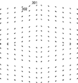
図3は、ベイヤ配列の原色カラーフィルタが設けられた撮像素子における焦点検出用画素の配置例を模式的に示す図である。ベイヤ配列では2×2画素を1単位として規則的にR,G,Bの各色画素が配置される。図3の例では、中央に存在するベイヤ配列の1単位に含まれるR画素の位置とB画素の位置に焦点検出用画素S1 301,S2 302が配置されている。焦点検出用画素S1,S2で水平方向に瞳分割する場合、焦点検出用画素S1,S2が有する開口の水平位置が異なるように配線層205が形成される。
FIG. 3 is a diagram schematically illustrating an arrangement example of focus detection pixels in an image sensor provided with a primary color filter having a Bayer array. In the Bayer array, R, G, and B color pixels are regularly arranged with 2 × 2 pixels as one unit. In the example of FIG. 3, focus
上述したように、焦点検出用画素301、302の位置で得られるはずのR画素とB画素の出力値は、欠陥画素補正回路105において補間により生成される。
As described above, the output values of the R pixel and the B pixel that should be obtained at the positions of the
図4は、撮像素子102における焦点検出用画素の配置例を模式的に示している。位相差検出方式による焦点検出を行うために必要な1対の像信号を生成するには、焦点検出用画素S1 301およびS2 302と同様の焦点検出用画素対が複数必要である。また、画面内の複数位置において焦点検出することができるよう、複数の焦点検出用画素対が撮像素子102の全体に離散的に配置されている。
FIG. 4 schematically illustrates an arrangement example of focus detection pixels in the
また、水平方向に瞳分割した焦点検出用画素対から得られる1対の像信号からは、撮影画面の横方向に輝度分布を有した被写体、例えば縦線に対しては焦点検出可能だが、縦方向に輝度分布を有する被写体、例えば横線に対しては焦点検出不能である。そのため、瞳分割方向が異なる(例えば垂直方向、斜め45°方向、135℃方向など)焦点検出用画素対がやはり撮像素子102の全体に離散的に配置される。
Further, from a pair of image signals obtained from a focus detection pixel pair obtained by dividing the pupil in the horizontal direction, focus detection is possible for an object having a luminance distribution in the horizontal direction of the shooting screen, for example, a vertical line. Focus detection is impossible for a subject having a luminance distribution in the direction, such as a horizontal line. For this reason, focus detection pixel pairs having different pupil division directions (for example, the vertical direction, the oblique 45 ° direction, and the 135 ° C. direction) are also discretely arranged on the
上述の通り、マイクロレンズの光軸ずれを考慮して開口位置を変化させた焦点検出用画素を設ける場合も同様であり、従って多数の異なる種類の焦点検出用画素対が撮像素子102の全体に離散的に配置される。また、図4に示すように、焦点検出用画素対の配置は均一ではなく、一見変則的な配置を有する。
As described above, the same applies to the case of providing focus detection pixels in which the aperture position is changed in consideration of the optical axis shift of the microlens. Accordingly, many different types of focus detection pixel pairs are provided in the
図5は、画素情報記憶部103が記憶する画素情報とそのデータ構造の例を模式的に示す図である。一つの画素情報は、画素の種類によらず、図5(a)に示すように、それぞれ固定ビット数を有する、ID領域501、オペランド領域502、および位置情報領域503を有する。なお、これら情報の格納順序は図示したものに限定されない。画素情報記憶部103は、図5(a)に示す形式のデータ(レコード)の集合体であり、配列として取り扱われてもよい。
FIG. 5 is a diagram schematically illustrating an example of pixel information stored in the pixel
ID領域501には、その画素が焦点検出用画素なのか、撮像用画素の欠陥画素なのか、また、欠陥画素の場合、その種類を示す情報が格納される。欠陥画素の種類は、例えば欠陥を補正する方法を示しても良く、ゲインを補正する欠陥、周囲から補間する欠陥、オフセットを補正する欠陥などの種類がある。
また、ID領域501には、ダミーIDが格納されることもある。ダミーIDの意味とその使用方法については後で説明する。
The
The
オペランド領域502には、ID領域501の内容によって異なる情報が格納される。例えばID領域501が焦点検出用画素を示す場合、例えば開口の種類を特定する情報(開口ID)が格納されてよい。また、ID領域501が欠陥画素を示す場合、例えば欠陥レベルを示す情報が格納されてよい。
The
位置情報領域503には、画素の位置を特定する情報が格納される。画素の位置情報は、絶対位置の情報(例えばXY座標)ではなく、他の欠陥画素または焦点検出用画素からの相対距離(画素数)の情報とする。このように、他の欠陥画素の位置からの相対距離で位置情報を記憶することにより、絶対位置情報を記憶する場合よりも位置情報領域503に必要なビット数を少なくすることができる。なお、相対距離を0とすることで、同一画素に対して複数の画素情報(例えば、焦点検出画素としての情報と欠陥画素としての情報)を記憶することもできる。
The
なお、相対距離は予め定められた画素のスキャン規則に従った距離であり、必ずしも最短距離であるとは限らない。例えば撮像素子の左上隅の画素から右方向に1ライン分画素をスキャンしたら、次のラインの左端の画素から右方向にスキャンする規則であれば、水平方向の位置が等しく、垂直方向に隣接する画素間の距離は1(水平)ライン分の画素数に等しい。なお、スキャン規則における最初の欠陥画素または焦点検出用画素に対する位置情報は、例えば0番目の画素からの相対距離を格納する。スキャン規則に従って現れる欠陥画素または焦点検出用画素の順番に従って画素情報を記憶することで、画素情報を順に読み出して用いることができる。 The relative distance is a distance according to a predetermined pixel scanning rule, and is not necessarily the shortest distance. For example, if one line of pixels is scanned rightward from the pixel at the upper left corner of the image sensor, the horizontal position is equal and the pixels are adjacent in the vertical direction if the rule is to scan rightward from the leftmost pixel of the next line. The distance between the pixels is equal to the number of pixels for one (horizontal) line. The position information for the first defective pixel or focus detection pixel in the scan rule stores, for example, a relative distance from the 0th pixel. By storing pixel information according to the order of defective pixels or focus detection pixels that appear according to the scan rule, the pixel information can be read out and used in order.
例えば、撮像素子102が横4000×縦3000画素を有する場合、画素の位置を絶対座標で表現するには、横(X)方向の座標と縦(Y)方向の座標のそれぞれに対して12ビット必要であるため、合計24ビットが必要である。
For example, when the
一方、画素間の相対距離であれば、16ビットもあれば65000画素分の距離を表現できる。欠陥画素は平均1/64000画素程度の発生確率であるため、十分対応可能である。また、本実施形態では欠陥画素以外に焦点検出用画素も離散的に配置されるため、16ビットで足りる場合が多いと考えられる。 On the other hand, if it is a relative distance between pixels, a distance of 65000 pixels can be expressed with 16 bits. Since defective pixels have an occurrence probability of about 1/64000 pixels on average, they can be sufficiently handled. In this embodiment, since the focus detection pixels are also discretely arranged in addition to the defective pixels, 16 bits may be sufficient in many cases.
しかしながら、16ビットで表現できる画素数よりも相対距離が大きい場合が発生する可能性がある。そのため、本実施形態では、位置情報領域503に割り当てたビット数で表現できる画素数を超える相対距離に対応するため、ダミーIDを用いる。ID領域501にダミーIDが格納されている場合には、位置情報領域503の情報は位置情報処理回路603のカウントダウンのみに用いられ、位置情報領域503に格納されている値に対応する画素を欠陥画素や焦点検出用画素とは扱わない。
However, there is a possibility that the relative distance is larger than the number of pixels that can be expressed by 16 bits. For this reason, in the present embodiment, a dummy ID is used to cope with a relative distance that exceeds the number of pixels that can be expressed by the number of bits assigned to the
具体的には、ダミーIDが格納された画素情報については、位置情報領域503の値をカウントダウンするだけで、他の処理は行わない。これによりダミーIDが格納された画素情報の位置情報領域503の値と、次の画素情報の位置情報領域503の値との合計により相対距離を表すことができる。ダミーIDを有する画素情報は繰り返されてもよい。これにより、まれに生じうる長大な相対距離にも対応可能である。従って、画素情報を記憶する際に、相対距離が位置情報領域503のビット数で対応できない場合、ダミーIDを格納した画素情報の位置情報と、それに続く、ダミーIDを格納しない画素情報との位置情報との合計により相対距離を表すようにする。
Specifically, for the pixel information in which the dummy ID is stored, only the value in the
図6は画素分離回路104および欠陥画素補正回路105において、画素情報記憶部103に記憶された画素情報から必要な情報を取得、生成する回路の構成例を示すブロック図である。
FIG. 6 is a block diagram illustrating a configuration example of a circuit that acquires and generates necessary information from the pixel information stored in the pixel
画素情報は画素情報記憶部103から読み出され、ID領域501は画素ID処理回路601に、オペランド領域502はオペランド処理回路602に、位置情報領域503は位置情報処理回路603にそれぞれロードされる。ここで、位置情報は上述の通り、他の欠陥画素または焦点検出用画素からの相対距離(画素数)を示す値である。
Pixel information is read from the pixel
位置情報処理回路603はダウンカウンタを有し、画素信号を処理するごとにカウントダウンする。位置情報処理回路603は、ダウンカウンタの値が0になるまで、”0”を出力する。この出力はインバータ604を通じて値”1”のBUSY信号として出力され、次の画素情報のロードを禁止する。ダウンカウンタの値が0になると、位置情報処理回路603の出力は”1”となる。これにより、インバータ604を通じてBUSY信号の値は”0”となり、次の画素情報のロードが許可される。
The position
位置情報処理回路603がカウントダウンしている間、画素ID処理回路601は画素IDを保持する。そしてID検知回路606は、保持されている画素IDが、ID指定レジスタ605に指定されている画素IDかどうかどうかを判別する。ID指定レジスタ605は、欠陥画素補正回路105と画素分離回路104で処理すべき画素の種類を制御部107から指定するために設けられている。
While the position
画素ID処理回路601に保持されている画素IDがID指定レジスタ605に指定されている画素IDであれば、ID検知回路606はANDゲート607に値”1”の信号を、それ以外の場合(ダミーIDの場合を含む)は値”0”の信号をANDゲート607に出力する。ANDゲート607は位置情報処理回路603の出力とID検知回路606の出力との論理積をタイミングフラグ(処理すべき欠陥画素・焦点検出用画素を示す欠陥フラグ)として出力する。また、ID検知回路606は、画素IDが欠陥の種類を示す情報の場合、その情報を出力する。
If the pixel ID held in the pixel
制御部107は、画素分離回路104のID指定レジスタ605には、焦点検出用画素IDのみを指定する。画素分離回路104では、オペランド処理回路602の出力するオペランド領域502の情報を、A像B像、垂直方向の瞳分割、水平方向の瞳分割など、焦点検出用画素の種類を特定する分類情報として扱う。
The
画素分離回路104では、オペランド領域502に格納された開口IDから焦点検出用画素の種類を判別し、同種のA像用焦点検出用画素とB像用焦点検出用画素の出力信号からA像とB像を生成する。そして、焦点検出回路108は、A像とB像のずれ量とずれ方向からデフォーカス量を計算する。なお、画素分離回路104は、焦点検出用画素の瞳分割方向が複数あれば、瞳分割方向ごとにA像およびB像を生成する。
The
一方、制御部107は、欠陥画素補正回路105のID指定レジスタ605には、欠陥種類IDに加え、焦点検出用画素IDも処理対象の画素として指定する。これにより、欠陥画素補正回路105では撮像用画素と焦点検出用画素の両方について画素補間処理を適用する。なお、焦点検出用画素に対する補間処理と、撮像用画素の欠陥画素に対する補間処理は同じであってもよいし、異ならせてもよい。撮像用画素の欠陥画素については、欠陥の種類およびレベルに応じた補間処理を行うようにしてもよい。
On the other hand, the
ダミーIDは関しては欠陥画素補正回路105でも画素分離回路104でもID指定レジスタ605に指定されないため、ID検知回路606の、欠陥画素の種類の出力には影響しない。
Since the dummy ID is not specified in the
このように、ID指定レジスタに指定されていないIDを有する画素情報については処理しないように構成することで、既存の回路での処理に影響を与えること無く、新たなIDを導入したり、新たなIDに対する処理を行う回路を追加することが容易に実現できる。例えば離散的に赤外画素を配置して、赤外画素処理回路を追加する場合、赤外画素のIDを有する画素情報を追加し、赤外画素処理回路のID指定レジスタ605に赤外画素のIDを指定すればよい。画素分離回路104や欠陥画素補正回路105では、赤外画素のIDは無視されるため、処理が影響を受けない。
In this way, by configuring so that pixel information having an ID not specified in the ID specification register is not processed, a new ID can be introduced or new information can be introduced without affecting the processing in the existing circuit. It is possible to easily add a circuit for performing processing for a unique ID. For example, when infrared pixels are discretely arranged and an infrared pixel processing circuit is added, pixel information having an ID of the infrared pixel is added, and the infrared pixel is stored in the ID designation register 605 of the infrared pixel processing circuit. What is necessary is just to specify ID. In the
以上説明したように、本実施形態によれば、撮像用画素の欠陥画素と焦点検出用画素の情報をまとめて管理し、撮像用画素の欠陥画素については欠陥の種類やレベルについての情報を含めることができるため、きめ細かい補間処理を行うことができる。また、画素の位置を特定する情報として他の撮像用画素の欠陥画素と焦点検出用画素からの相対距離を用いることで、画素情報あたりに必要な情報量を削減することができ、メモリ使用効率を向上させることができる。 As described above, according to the present embodiment, information on defective pixels and focus detection pixels of the imaging pixel is managed together, and information on the type and level of the defect is included for the defective pixels of the imaging pixel. Therefore, fine interpolation processing can be performed. In addition, by using the relative distance between the defective pixel of another imaging pixel and the focus detection pixel as information for specifying the pixel position, the amount of information required per pixel information can be reduced, and the memory usage efficiency Can be improved.
また、欠陥画素や焦点検出画素の処理回路を、指定されたIDを有する画素情報に対応する画素だけを処理するように構成することにより、既存の処理回路の処理に影響を与えること無しに、新たな画素の種類や処理回路を追加することができる。 Further, by configuring the processing circuit of the defective pixel and the focus detection pixel so as to process only the pixel corresponding to the pixel information having the specified ID, without affecting the processing of the existing processing circuit, New pixel types and processing circuits can be added.
(第2の実施形態)
次に、図7を参照して、本発明の第2の実施形態について説明する。本実施形態においても第1の実施形態と同様、本発明に係る画素情報記憶装置を適用したデジタルカメラを例にして説明する。図7において、第1の実施形態と同様の構成については図1と同じ参照数字を付してある。
(Second Embodiment)
Next, a second embodiment of the present invention will be described with reference to FIG. Also in this embodiment, as in the first embodiment, a digital camera to which the pixel information storage device according to the present invention is applied will be described as an example. In FIG. 7, the same reference numerals as those in FIG. 1 are assigned to the same configurations as those in the first embodiment.
第1の実施形態においては、欠陥画素補正回路105と画素分離回路104が画素情報記憶部103に並列に接続された構成であった。それに対し、本実施形態では、画素分離回路104と欠陥画素補正回路105とが直列に配線され、第1の実施形態における画素情報記憶部と同様の画素情報が記憶される第1の画素情報記憶部103に加え、第2の画素情報記憶部109が追加されている。第2の画素情報記憶部109では、第1の画素情報記憶部109に記憶される画素情報とは異なる画素情報が記憶されている。
In the first embodiment, the defective
画素分離回路104は、撮像用画素については出力をそのまま欠陥画素補正回路105に供給し、焦点検出用画素についてはその出力を特別な値に置き換えて欠陥画素補正回路105に供給する。欠陥画素補正回路105は、画素分離回路104の出力値から焦点検出用画素の出力を判別し、補間処理の対象とする。焦点検出用画素の出力であることを示す特別な値は、ゼロなど、画像としては階調が重要でないと思われる領域の値である。値ゼロの撮像用画素があった場合、その値を例えば1に置き換えて出力する。
The
撮像素子の製造時に検出した欠陥画素の情報は第1の画素情報記憶部103に記憶されているが、製造時には正常な画素とみなされていた画素が、経年劣化などにより欠陥画素になる場合がある。そのため、本実施形態では、第1の画素情報記憶部103に画素情報を記憶した後で経年劣化等により増えた欠陥画素の画素情報を記憶するために第2の画素情報記憶部109を追加している。第2の画素情報記憶部109への情報の追加は、例えば装置の起動時に欠陥画素の検出処理を行い、新たに欠陥画素と判別された画素が見つかった際に行う等、任意のタイミングで行うことができる。
Information on defective pixels detected at the time of manufacturing the image sensor is stored in the first pixel
欠陥画素補正回路105は、第2の画素情報記憶部109に記憶されている画素情報は第1の実施形態と同様に図6に示した回路で処理する。それに加え、画素信号値が特別な値である画素についても補間処理を行う。画素信号値が特別な値である画素に対してどのような補間処理を行うかは任意である。
The defective
欠陥画素補正回路105には、製造時に生じた欠陥画素を知らせる必要がある。そのため、本実施形態では、欠陥画素についても焦点検出用画素として第1の画素情報記憶部103に記憶しておく。ただし、画素分離回路104が焦点検出用画素として処理しないように、開口IDに特別な値を指定しておく。画素分離回路104は、開口IDに特別な値が含まれている場合、対応する画素を欠陥画素と判別し、出力値を特別な値(ゼロ)に置き換えて欠陥画素補正回路105に供給する。
It is necessary to notify the defective
本実施形態によれば、経時劣化によって生じた欠陥画素についても補間処理の対象とすることができる。 According to the present embodiment, defective pixels caused by deterioration over time can also be targeted for interpolation processing.
(第3の実施形態)
次に、図8を参照して、本発明の第3の実施形態について説明する。本実施形態においても第1の実施形態と同様、本発明に係る画素情報記憶装置を適用したデジタルカメラを例にして説明する。図8において、第1の実施形態と同様の構成については図1と同じ参照数字を付してある。
(Third embodiment)
Next, a third embodiment of the present invention will be described with reference to FIG. Also in this embodiment, as in the first embodiment, a digital camera to which the pixel information storage device according to the present invention is applied will be described as an example. In FIG. 8, the same reference numerals as those in FIG. 1 are assigned to the same configurations as those in the first embodiment.
本実施形態では、画素情報記憶部に相当する第1の画素情報記憶部103に加え、第3の画素情報記憶部110が追加されている。また、第1および第3の画素情報記憶部103,110のいずれかを、制御部107の制御に応じて選択的に画素分離回路104と欠陥画素補正回路105と接続するスイッチ111が設けられている。
In the present embodiment, a third pixel
撮像素子102が複数の読み出しモードを有する場合がある。例えば、すべての画素を読み出すモードに加え、画素を間引いて読み出すモードや、画素を加算してから読み出すモードなどがある。
間引きや加算を行う場合、全ての画素を読み出す場合と読み出される画素数が異なる。このように、読み出しモードによって読み出す画素数が異なる場合、画素情報に含まれる位置情報についても読み出しモードに応じた相対距離とする必要がある。
The
When thinning or addition is performed, the number of pixels to be read is different from the case of reading all pixels. As described above, when the number of pixels to be read is different depending on the reading mode, the positional information included in the pixel information needs to be a relative distance corresponding to the reading mode.
本実施形態では、読み出される画素数が読み出しモードに応じて2通り存在する場合に、読み出し画素数に応じた画素位置を有する画素情報を記憶した画素情報記憶部を用意し、読み出しモードに応じて制御部107がスイッチ111を適切に切り替える。例えば、第1の画素情報記憶部103が全画素を読み出すモードに対応する画素情報を記憶し、第3の画素情報記憶部110が、間引き読み出しや加算読みだしのように全画素より少ない特定数の画素を読み出すモードに対応する画素情報を記憶している。
In the present embodiment, when there are two types of pixels to be read out according to the read mode, a pixel information storage unit that stores pixel information having pixel positions according to the number of read pixels is prepared. The
なお、図8では、第1および第3の画素情報記憶部103,110を物理的に異なる記憶部とし、スイッチ111で接続を切り替える構成を示した。しかし、第1および第3の画素情報記憶部103,110を、同一の記憶装置の異なるアドレス空間として実装してもよい。
FIG. 8 shows a configuration in which the first and third pixel
(第4の実施形態)
次に図9を参照して本発明の第4の実施形態について説明する。本実施形態においても第3の実施形態と同様、本発明に係る画素情報記憶装置を適用したデジタルカメラを例にして説明する。
(Fourth embodiment)
Next, a fourth embodiment of the present invention will be described with reference to FIG. In the present embodiment, as in the third embodiment, a digital camera to which the pixel information storage device according to the present invention is applied will be described as an example.
図9は撮像素子102における焦点検出用画素の別の配置例を模式的に示している。
901は撮像素子における画素配置領域の全体を示し、図9(a)の例では902で指し示す中央部のみに焦点検出用画素が配置されている。このように、撮像素子の部分領域、特に中央部のみに焦点検出用画素を配置するのは、撮像する視野の中央部分に主被写体が存在する場合が多いことや、焦点検出用画素の配置が限定的な範囲である方が撮像素子の設計上の制約が小さいことなどの理由による。図9(a)に示すように焦点検出用画素が配置された撮像素子を備えるデジタルカメラは、視野の中央部の被写体に対して焦点検出する仕様になる。
FIG. 9 schematically shows another arrangement example of focus detection pixels in the
第3の実施形態で示した間引きや加算読み出しのモードは撮影時のビューファインダーや動画撮影に利用するものであるが、そのようなモードでは焦点検出用画素の密度が高くなるように画素を配置すると、焦点検出精度が良くなる。 The thinning and addition readout modes shown in the third embodiment are used for viewfinder and moving image shooting at the time of shooting. In such a mode, pixels are arranged so that the density of focus detection pixels is high. Then, focus detection accuracy is improved.
一方で、ある画素領域において焦点検出用画素の配置密度を高めると、その領域内での撮像用画素の配置密度が低下するため、画質が低下する。具体例としては、繰り返しパターンを含む被写体を撮影した時に、繰り返しパターンの空間周波数と焦点検出用画素の配置の空間周波数とが干渉して低い疑似周波数成分を発生させてしまう。そのような低い周波数成分は間引き読み出しによっても発生するが、間引き読み出しで発生する低周波数成分は撮像素子の画素配置領域全体に一様に発生するため目立たない。しかし、焦点検出用画素の配置密度が領域によって異なる場合、配置密度が高い領域と低い領域とでは発生する低周波成分が異なる。図9(a)の例では、撮像素子の画素配置領域の中央部にのみ焦点検出用画素が配置されているため、中央部に発生する疑似低周波成分が他の領域よりも多くなり、視覚的に強い違和感を与えてしまう。 On the other hand, when the arrangement density of focus detection pixels in a certain pixel area is increased, the arrangement density of imaging pixels in the area is lowered, and the image quality is lowered. As a specific example, when a subject including a repetitive pattern is photographed, the spatial frequency of the repetitive pattern interferes with the spatial frequency of the focus detection pixel arrangement to generate a low pseudo frequency component. Such a low frequency component is also generated by thinning readout, but the low frequency component generated by thinning readout is uniformly generated in the entire pixel arrangement region of the image sensor, and thus is not conspicuous. However, when the arrangement density of the focus detection pixels differs depending on the area, the generated low frequency component differs between the area where the arrangement density is high and the area where the arrangement density is low. In the example of FIG. 9A, since the focus detection pixel is arranged only in the central portion of the pixel arrangement region of the image sensor, the pseudo low frequency component generated in the central portion is larger than in other regions, and the visual Give a strong sense of incongruity.
本実施形態では、焦点検出用画素が撮像素子の部分領域に配置され、かつ間引き読み出しモード時は、焦点検出用画素が配置されていない領域に、焦点検出用画素と同じ配置密度で欠陥画素が存在するものとして取り扱う。図9(a)の例で言えば、902で示す部分領域以外の領域の少なくとも一部について、焦点検出用画素と同じ配置密度(かつ配置規則)で、欠陥画素が存在しているような画素情報を記憶した第2の画素情報記憶部109を用意しておく。そして、焦点検出用画素が撮像素子の部分領域に配置され、かつ間引き読み出しモード時には、間引き読み出しモード用の画素情報を第2の画素情報記憶部109から参照する。
In the present embodiment, when the focus detection pixels are arranged in the partial area of the image sensor and in the thinning readout mode, defective pixels are arranged at the same arrangement density as the focus detection pixels in the area where the focus detection pixels are not arranged. Treat as existing. In the example of FIG. 9A, a pixel in which a defective pixel exists with the same arrangement density (and arrangement rule) as the focus detection pixels in at least a part of the area other than the
これにより、焦点検出用画素の配置領域と非配置領域とで生じる低周波成分の差を低減もしくは解消することができ、視覚的な違和感を低減もしくは解消することができる。図9(b)は、間引き読み出し時における欠陥画素と焦点検出用画素の配置例を示している。図9(b)において、焦点検出用画素は図9(a)と同様、中央部のみに配置されており、他の領域では欠陥画素が配置されている。 Thereby, the difference of the low frequency component which arises with the arrangement | positioning area | region of a focus detection pixel and a non-arrangement area | region can be reduced or eliminated, and visual discomfort can be reduced or eliminated. FIG. 9B shows an arrangement example of defective pixels and focus detection pixels at the time of thinning readout. In FIG. 9B, the focus detection pixels are arranged only in the center as in FIG. 9A, and defective pixels are arranged in other regions.
なお、全画素を読みだして静止画を記録する場合のように、間引き読み出し時よりも焦点検出用画素の密度が十分低くなる場合には、焦点検出用画素が配置された領域だけを補正しても視覚的に目立たない。そのため、焦点検出用画素が配置されない領域について欠陥画素を配置せず、補正が必要な領域のみを必要に応じて欠陥画素補正することができる。 Note that if the density of focus detection pixels is sufficiently lower than when thinned out, as in the case where all pixels are read and a still image is recorded, only the area where the focus detection pixels are arranged is corrected. Even visually inconspicuous. Therefore, it is possible to correct a defective pixel as needed only in a region where correction is necessary without arranging defective pixels in a region where focus detection pixels are not arranged.
本実施形態によれば、読み出し画素数の異なる読み出しモードが存在する場合でも対応することができる。
以上、本発明の好ましい実施形態について説明したが、本発明はこれらの実施形態に限定されず、その要旨の範囲内で種々の変形及び変更が可能である。
According to the present embodiment, it is possible to cope with a case where there are readout modes with different numbers of readout pixels.
As mentioned above, although preferable embodiment of this invention was described, this invention is not limited to these embodiment, A various deformation | transformation and change are possible within the range of the summary.
Claims (20)
撮像用画素の欠陥画素と焦点検出用画素との各々について、
撮像用画素の欠陥画素か焦点検出用画素かを示す情報を格納する第1の領域と、
撮像用画素の欠陥画素については第1の情報を、焦点検出用画素については前記第1の情報を含まない第2の情報を格納する第2の領域と、
画素の位置を特定する情報を格納する位置情報領域と、
を有する画素情報を記憶し、
前記第1の領域、前記第2の領域、および前記位置情報領域の各々は固定ビット数を有し、
前記位置情報領域には、前記画素の位置を特定する情報として、他の撮像用画素の欠陥画素もしくは他の焦点検出用画素からの、予め定められた画素のスキャン規則に従った相対距離を記憶することを特徴とする画素情報管理装置。 A pixel information management device that stores information on defective pixels and focus detection pixels of imaging pixels among pixels of the imaging element,
For each of the defective pixel and the focus detection pixel of the imaging pixel,
A first area storing information indicating whether the imaging pixel is a defective pixel or a focus detection pixel;
A second area that stores first information for defective pixels of the imaging pixels, and second information that does not include the first information for focus detection pixels;
A position information area for storing information for specifying the position of the pixel;
Storing pixel information having
Each of the first area, the second area, and the position information area has a fixed number of bits;
In the position information area, a relative distance in accordance with a predetermined pixel scanning rule from a defective pixel of another imaging pixel or another focus detection pixel is stored as information for specifying the position of the pixel. A pixel information management device.
撮像用画素の欠陥画素と焦点検出用画素との各々について、
撮像用画素の欠陥画素か焦点検出用画素かを示す情報を格納する第1の領域と、
撮像用画素の欠陥画素については第1の情報を、焦点検出用画素については前記第1の情報を含まない第2の情報を格納する第2の領域と、
画素の位置を特定する情報を格納する位置情報領域と、
をそれぞれ異なる領域に有する画素情報を記憶し、
前記位置情報領域には、前記画素の位置を特定する情報として、他の撮像用画素の欠陥画素もしくは他の焦点検出用画素からの相対距離を記憶することを特徴とする画素情報管理装置。 A pixel information management device that stores information on defective pixels and focus detection pixels of imaging pixels among pixels of the imaging element,
For each of the defective pixel and the focus detection pixel of the imaging pixel,
A first area storing information indicating whether the imaging pixel is a defective pixel or a focus detection pixel;
A second area that stores first information for defective pixels of the imaging pixels, and second information that does not include the first information for focus detection pixels;
A position information area for storing information for specifying the position of the pixel;
Store pixel information each having a different area,
In the position information area, a relative distance from a defective pixel of another imaging pixel or another focus detection pixel is stored as information for specifying the position of the pixel.
前記画素情報管理装置が、撮像用画素の欠陥画素と焦点検出用画素との各々について、前記位置情報領域に前記読み出される画素の数に対応した前記画素の位置を特定する情報を格納した複数の画素情報を記憶することを特徴とする請求項1乃至請求項7のいずれか1項に記載の画素情報管理装置。 The image sensor has a plurality of readout modes with different numbers of pixels to be read out,
The pixel information management device stores a plurality of pieces of information for specifying the positions of the pixels corresponding to the number of pixels to be read in the position information area for each of the defective pixels and the focus detection pixels of the imaging pixels. 8. The pixel information management apparatus according to claim 1, wherein pixel information is stored.
前記画素情報管理装置が、前記間引き読み出しされるモードに対応した前記画素情報として、前記撮像素子の前記部分領域以外の領域に、前記焦点検出用画素と同様の配置密度で前記撮像用画素の欠陥画素が存在するような前記画素情報を記憶することを特徴とする請求項9記載の画素情報管理装置。 When the focus detection pixels are arranged in a partial region of the image sensor and the image sensor has a mode in which thinning readout is performed,
As the pixel information corresponding to the thinning-out read mode, the pixel information management device has defects in the imaging pixels in the area other than the partial area of the imaging element at the same arrangement density as the focus detection pixels. The pixel information management apparatus according to claim 9, wherein the pixel information is stored such that a pixel exists.
請求項1乃至請求項7、請求項9、および請求項10のいずれか1項に記載の画素情報管理装置とを有する撮像装置であって、
前記画素情報のうち、焦点検出用画素を示す情報が前記第1の領域に格納された画素情報を用いて、前記撮像素子が有する焦点検出用画素を判別し、焦点検出用画素の出力信号から位相差検出方式の焦点検出用の像信号を生成する手段と、
前記画素情報のうち、撮像用画素の欠陥画素または焦点検出用画素を示す情報が前記第1の領域に格納された画素情報を用いて、撮像用画素の欠陥画素または焦点検出用画素の位置の信号を補間により生成する手段と、を有することを特徴とする撮像装置。 An imaging device having imaging pixels and focus detection pixels;
An image pickup apparatus comprising the pixel information management device according to any one of claims 1 to 7, claim 9, and claim 10,
Of the pixel information, information indicating a focus detection pixel is used to determine a focus detection pixel included in the image sensor using pixel information stored in the first region, and an output signal of the focus detection pixel is used. Means for generating an image signal for focus detection of a phase difference detection method;
Among the pixel information, information indicating a defective pixel or focus detection pixel of the imaging pixel is stored in the first area, and the position of the defective pixel or focus detection pixel of the imaging pixel is detected. Means for generating a signal by interpolation.
前記撮像用画素の欠陥画素と、前記焦点検出用画素との各々について、撮像用画素の欠陥画素か、焦点検出用画素かを示す情報を格納する第1の領域と、撮像用画素の欠陥画素については第1の情報を、焦点検出用画素については前記第1の情報を含まない第2の情報を格納する第2の領域と、画素の位置を特定する情報を格納する位置情報領域と、をそれぞれ異なる領域に有する画素情報を記憶する画素情報管理装置とを有する撮像装置であって、
前記画素情報のうち、焦点検出用画素を示す情報が前記第1の領域に格納された画素情報を用いて、前記撮像素子が有する焦点検出用画素を判別し、焦点検出用画素の出力信号から位相差検出方式の焦点検出用の像信号を生成する手段と、
前記画素情報のうち、撮像用画素の欠陥画素または焦点検出用画素を示す情報が前記第1の領域に格納された画素情報を用いて、前記撮像用画素の欠陥画素または前記焦点検出用画素の位置の信号を補間により生成する手段と、を有することを特徴とする撮像装置。 An imaging device having imaging pixels and at least one focus detection pixel;
For each of the defective pixel of the imaging pixel and the focus detection pixel, a first area for storing information indicating whether the pixel is a defective pixel of the imaging pixel or a focus detection pixel, and the defective pixel of the imaging pixel A first information for a focus detection pixel , a second area for storing second information not including the first information for a focus detection pixel , a position information area for storing information for specifying the position of the pixel, Each having a pixel information management device that stores pixel information in different regions,
Of the pixel information, information indicating a focus detection pixel is used to determine a focus detection pixel included in the image sensor using pixel information stored in the first region, and an output signal of the focus detection pixel is used. Means for generating an image signal for focus detection of a phase difference detection method;
Of the pixel information, information indicating a defective pixel or focus detection pixel of the imaging pixel is stored in the first area, and the defective pixel of the imaging pixel or the focus detection pixel is detected. Means for generating a position signal by interpolation.
前記画素情報管理装置が、撮像用画素の欠陥画素と、焦点検出用画素との各々について、前記位置情報領域に前記読み出される画素の数に対応した前記画素の位置を特定する情報を格納した複数の画素情報を有することを特徴とする請求項12乃至請求項18のいずれか1項に記載の撮像装置。 The image sensor has a plurality of readout modes with different numbers of pixels to be read out,
The pixel information management device stores a plurality of pieces of information for specifying the positions of the pixels corresponding to the number of pixels to be read in the position information area for each of the defective pixels of the imaging pixels and the focus detection pixels. The image pickup apparatus according to claim 12, further comprising: pixel information.
前記画素情報管理装置が、前記間引き読み出しされるモードに対応した前記画素情報として、前記撮像素子の前記部分領域以外の領域に、前記焦点検出用画素と同様の配置密度で前記撮像用画素の欠陥画素が存在するような前記画素情報を有することを特徴とする請求項19に記載の撮像装置。 When the focus detection pixels are arranged in a partial region of the image sensor and the image sensor has a mode in which thinning readout is performed,
As the pixel information corresponding to the thinning-out read mode, the pixel information management device has defects in the imaging pixels in the area other than the partial area of the imaging element at the same arrangement density as the focus detection pixels. The imaging apparatus according to claim 19, comprising the pixel information such that a pixel exists.
Priority Applications (3)
| Application Number | Priority Date | Filing Date | Title |
|---|---|---|---|
| JP2012128406A JP6027777B2 (en) | 2012-04-06 | 2012-06-05 | Pixel information management device and imaging device using the same |
| US13/800,603 US8963910B2 (en) | 2012-04-06 | 2013-03-13 | Pixel information management apparatus and image capture apparatus using the same |
| CN201310110413.0A CN103369265B (en) | 2012-04-06 | 2013-04-01 | Pixel information management apparatus and image capture apparatus using the same |
Applications Claiming Priority (3)
| Application Number | Priority Date | Filing Date | Title |
|---|---|---|---|
| JP2012087932 | 2012-04-06 | ||
| JP2012087932 | 2012-04-06 | ||
| JP2012128406A JP6027777B2 (en) | 2012-04-06 | 2012-06-05 | Pixel information management device and imaging device using the same |
Publications (3)
| Publication Number | Publication Date |
|---|---|
| JP2013232873A JP2013232873A (en) | 2013-11-14 |
| JP2013232873A5 JP2013232873A5 (en) | 2015-04-23 |
| JP6027777B2 true JP6027777B2 (en) | 2016-11-16 |
Family
ID=49291922
Family Applications (1)
| Application Number | Title | Priority Date | Filing Date |
|---|---|---|---|
| JP2012128406A Expired - Fee Related JP6027777B2 (en) | 2012-04-06 | 2012-06-05 | Pixel information management device and imaging device using the same |
Country Status (3)
| Country | Link |
|---|---|
| US (1) | US8963910B2 (en) |
| JP (1) | JP6027777B2 (en) |
| CN (1) | CN103369265B (en) |
Families Citing this family (11)
| Publication number | Priority date | Publication date | Assignee | Title |
|---|---|---|---|---|
| JP6346439B2 (en) * | 2013-01-07 | 2018-06-20 | キヤノン株式会社 | Imaging apparatus and control method thereof |
| US9826174B2 (en) * | 2013-03-26 | 2017-11-21 | Samsung Electronics Co., Ltd | Image processing apparatus and method |
| KR102121531B1 (en) * | 2013-12-10 | 2020-06-10 | 삼성전자주식회사 | Apparatus and Method for Controlling a Focus Detectable Image Sensor |
| JP2016058451A (en) * | 2014-09-05 | 2016-04-21 | キヤノン株式会社 | Sensor and camera |
| TWI565323B (en) * | 2015-09-02 | 2017-01-01 | 原相科技股份有限公司 | Imaging device for distinguishing foreground and operating method thereof, and image sensor |
| US10440299B2 (en) * | 2015-09-04 | 2019-10-08 | Apple Inc. | Correcting pixel defects based on defect history in an image processing pipeline |
| KR102575281B1 (en) * | 2016-10-14 | 2023-09-06 | 한화비전 주식회사 | Apparatus for writing information on defect pixels, apparatus for correcting defect pixels, and method thereof |
| US10536621B2 (en) * | 2016-10-19 | 2020-01-14 | Canon Kabushiki Kaisha | Image capturing apparatus, storage medium and controlling method for correcting a second image by correcting a pixel value of the second image corresponding to a detected defective pixel |
| JP6765953B2 (en) * | 2016-12-22 | 2020-10-07 | キヤノン株式会社 | Imaging device and its control method |
| JP2018157371A (en) * | 2017-03-17 | 2018-10-04 | キヤノン株式会社 | Imaging apparatus and method of correcting defective pixels |
| GB2572662B (en) * | 2018-10-05 | 2020-06-03 | Res & Innovation Uk | Raman spectrometer |
Family Cites Families (9)
| Publication number | Priority date | Publication date | Assignee | Title |
|---|---|---|---|---|
| JP2565262B2 (en) * | 1987-10-17 | 1996-12-18 | ソニー株式会社 | Image defect correction device for solid-state imaging device |
| JP3360409B2 (en) * | 1994-04-15 | 2002-12-24 | ソニー株式会社 | Imaging signal defect detection and correction apparatus, imaging signal defect detection and correction method, and imaging signal processing method |
| JP3866017B2 (en) * | 2000-06-30 | 2007-01-10 | 三菱電機株式会社 | Defective pixel detection device and recording medium on which defective pixel detection program is recorded |
| JP2007295312A (en) * | 2006-04-25 | 2007-11-08 | Olympus Imaging Corp | Digital camera |
| JP5019581B2 (en) * | 2007-01-29 | 2012-09-05 | キヤノン株式会社 | Imaging apparatus and imaging system |
| JP5180795B2 (en) * | 2007-12-10 | 2013-04-10 | キヤノン株式会社 | Imaging apparatus and control method thereof |
| JP5552214B2 (en) | 2008-03-11 | 2014-07-16 | キヤノン株式会社 | Focus detection device |
| JP5341479B2 (en) | 2008-11-06 | 2013-11-13 | キヤノン株式会社 | Imaging device |
| JP5625286B2 (en) * | 2009-08-19 | 2014-11-19 | 株式会社ニコン | Imaging device |
-
2012
- 2012-06-05 JP JP2012128406A patent/JP6027777B2/en not_active Expired - Fee Related
-
2013
- 2013-03-13 US US13/800,603 patent/US8963910B2/en not_active Expired - Fee Related
- 2013-04-01 CN CN201310110413.0A patent/CN103369265B/en not_active Expired - Fee Related
Also Published As
| Publication number | Publication date |
|---|---|
| US8963910B2 (en) | 2015-02-24 |
| CN103369265B (en) | 2017-04-12 |
| JP2013232873A (en) | 2013-11-14 |
| CN103369265A (en) | 2013-10-23 |
| US20130265295A1 (en) | 2013-10-10 |
Similar Documents
| Publication | Publication Date | Title |
|---|---|---|
| JP6027777B2 (en) | Pixel information management device and imaging device using the same | |
| JP5740465B2 (en) | Imaging apparatus and defective pixel correction method | |
| JP5589146B2 (en) | Imaging device and imaging apparatus | |
| US8730545B2 (en) | Color imaging element, imaging device, and storage medium storing a control program for imaging device | |
| US8723991B2 (en) | Color imaging element, imaging device, and storage medium storing an imaging program | |
| US8736743B2 (en) | Color imaging element, imaging device, and storage medium storing a control program for imaging device | |
| US8723992B2 (en) | Color imaging element, imaging device, and storage medium storing an imaging program | |
| JP2007201530A (en) | Pixel defect correction apparatus | |
| US8842214B2 (en) | Color imaging element, imaging device, and storage medium storing an imaging program | |
| JPWO2013046827A1 (en) | Image processing apparatus, method and program, and imaging apparatus | |
| JPWO2013099637A1 (en) | Color imaging device and imaging apparatus | |
| JP5456206B2 (en) | IMAGING DEVICE, IMAGING DEVICE CONTROL PROGRAM, AND IMAGING DEVICE CONTROL METHOD | |
| JP5524406B2 (en) | Imaging apparatus and imaging program | |
| JP5539583B2 (en) | Color imaging device, imaging device, and imaging program | |
| JP2010212788A (en) | Image capturing apparatus, defective pixel correction method, and electronic information apparatus | |
| JP2011166422A (en) | Imaging apparatus | |
| JP5709472B2 (en) | Signal processing device | |
| JP5206176B2 (en) | Image converter | |
| JP2005210164A (en) | Correction apparatus for defective pixel | |
| JP5968145B2 (en) | Image processing apparatus and control method thereof | |
| JP5624227B2 (en) | IMAGING DEVICE, IMAGING DEVICE CONTROL METHOD, AND CONTROL PROGRAM | |
| JP5607267B2 (en) | IMAGING DEVICE, IMAGING DEVICE CONTROL METHOD, AND CONTROL PROGRAM | |
| JP6045247B2 (en) | Image processing apparatus, control method thereof, and control program | |
| JP2016158041A (en) | Image processor and image processing method |
Legal Events
| Date | Code | Title | Description |
|---|---|---|---|
| A521 | Request for written amendment filed |
Free format text: JAPANESE INTERMEDIATE CODE: A523 Effective date: 20150309 |
|
| A621 | Written request for application examination |
Free format text: JAPANESE INTERMEDIATE CODE: A621 Effective date: 20150309 |
|
| A977 | Report on retrieval |
Free format text: JAPANESE INTERMEDIATE CODE: A971007 Effective date: 20160322 |
|
| A131 | Notification of reasons for refusal |
Free format text: JAPANESE INTERMEDIATE CODE: A131 Effective date: 20160325 |
|
| A521 | Request for written amendment filed |
Free format text: JAPANESE INTERMEDIATE CODE: A523 Effective date: 20160520 |
|
| TRDD | Decision of grant or rejection written | ||
| A01 | Written decision to grant a patent or to grant a registration (utility model) |
Free format text: JAPANESE INTERMEDIATE CODE: A01 Effective date: 20160916 |
|
| A61 | First payment of annual fees (during grant procedure) |
Free format text: JAPANESE INTERMEDIATE CODE: A61 Effective date: 20161017 |
|
| R151 | Written notification of patent or utility model registration |
Ref document number: 6027777 Country of ref document: JP Free format text: JAPANESE INTERMEDIATE CODE: R151 |
|
| LAPS | Cancellation because of no payment of annual fees |